Characterization of Next Generation Thin Low-K and Low-Loss
9
This article has been accepted for inclusion in a future issue of this journal. Content is final as presented, with the exception of pagination. IEEE TRANSACTIONS ON ADVANCED PACKAGING 1 Characterization of Next Generation Thin Low-K and Low-Loss Organic Dielectrics From 1 to 110 GHz Seunghyun Hwang, Sunghwan Min, Member, IEEE, Madhavan Swaminathan, Fellow, IEEE, Venkatesan Venkatakrishnan, Hunter Chan, Fuhan Liu, Venky Sundaram, Scott Kennedy, Dirk Baars, Benjamin Lacroix, Yuan Li, and John Papapolymerou, Senior Member, IEEE Abstract—This paper presents, for the first time, characteriza- tion results of next generation dielectric core and build up material called RXP, which has low dielectric constant (2.93–3.48) and low loss tangent (0.0037–0.006) up to 110 GHz. Unlike LCP, this mate- rial can be made ultra-thin with low processing temperature and is ideally suited for mobile applications. Causal models suitable for high frequency applications have been extracted by measuring the response of cavity resonators using vector network analyzer and surface profiler. Index Terms—Cavity resonator, dielectric constant, loss tangent, millimeter-wave, surface roughness. I. INTRODUCTION L OW COST, compact size, and high performance com- bined with increasing system complexity have brought the need for higher levels of integration in RF front-end module. System on package (SOP) has been used as a solution for sup- porting the convergence of multiple RF front-end modules by providing more functionalities in the package through integra- tion of passive components such as inductors, capacitors, and resistors [1]. Embedded passive technology is a key enabling technology for higher levels of integration in SOP. This tech- nology requires advanced fabrication techniques and dielectric materials in order to satisfy very demanding performance re- quirements. Low temperature co-fired ceramic (LTCC) technology has allowed the fabrication and integration of three-dimensional circuits. Although LTCC technology has significantly lower loss at high frequencies and lower coefficient of thermal expan- sion (CTE) than FR4 [2], LTCC technology provides limited integration capability [3]. In addition, LTCC technology has higher cost as compared to an organic based solution [4]. As an alternative to LTCC technology, an organic material that has become popular recently is liquid crystalline polymer (LCP), which has low loss (loss – up to 110 Manuscript received December 17, 2008; revised May 02, 2009. This work was recommended for publication by Associate Editor L.-T. Hwang upon eval- uation of the reviewers comments. S. Hwang, S. Min, M. Swaminathan, V. Venkatakrishnan, H. Chan, F. Liu, V. Sundaram, B. Lacroix, Y. Li, and J. Papapolymerou are with the School of Electrical and Computer Engineering, Georgia Institute of Technology, Atlanta, GA 30332 USA. S. Kennedy and D. Baars are with the Rogers Corporation, Rogers, CT 06263 USA. Color versions of one or more of the figures in this paper are available online at http://ieeexplore.ieee.org. Digital Object Identifier 10.1109/TADVP.2009.2023413 Fig. 1. Embedded passive and active module using RXP. GHz), low cost ($5/ft for 2-mil single-clad low-melt LCP) [5], and is compatible with PCB manufacturing processes. However, relatively high processing temperature (290 C) and limitations on package integration density are still bottlenecks for the adoption of LCP technology for mobile cell phone applications [6]. Recently, a new dielectric material has been introduced, which can be a replacement for LCP for ultra-thin substrates re- quired in mobile applications [7], [8]. In [7], high Q embedded inductors have been developed in the core dielectric material (RXP1). In addition, a thin build-up dielectric material (RXP4) has been successfully developed with fine line and low CTE capability [8]. As shown in Fig. 1, RF front-end modules with a total thickness of less than 0.3 mm can be constructed using a combination of RXP1 and RXP4 materials, which can contain interconnects, electromagnetic band-gap (EBG) structures, embedded passives and embedded actives with mixed signal (digital and RF) ICs. Details regarding the fabrication process of RXP can be found in [9]. Since mobile applications operate at high frequencies, it is necessary to characterize materials as a function of frequency. Microwave techniques for characterizing materials can be broadly classified into two techniques, namely nonresonant and resonant based methods. Nonresonant based methods use wave propagation on a transmission line to extract dielectric properties over a continuous frequency range of interest [10] whereas resonant based methods are used to extract dielectric properties at discrete frequencies corresponding to the resonant frequency of the device [11]. The advantage of the resonator based method is its sensitivity to small changes in low loss di- electric properties [12]. A resonant based method has therefore been used in this paper. In [12], split-cylinder resonator was used to extract material properties. However, asymmetrical movement of the two termi- nations results in considerable measurement error especially at high frequencies using this approach. Parallel-plate cavity res- onator based on analytical solutions for estimating the resonant frequency was introduced in [13]. Although this resonator is simple to fabricate, the analytical equations are inaccurate for 1521-3323/$26.00 © 2009 IEEE Authorized licensed use limited to: Georgia Institute of Technology. Downloaded on October 10, 2009 at 13:16 from IEEE Xplore. Restrictions apply.
Transcript of Characterization of Next Generation Thin Low-K and Low-Loss

This article has been accepted for inclusion in a future issue of this journal. Content is final as presented, with the exception of pagination.
IEEE TRANSACTIONS ON ADVANCED PACKAGING 1
Characterization of Next Generation Thin Low-K andLow-Loss Organic Dielectrics From 1 to 110 GHz
Seunghyun Hwang, Sunghwan Min, Member, IEEE, Madhavan Swaminathan, Fellow, IEEE,Venkatesan Venkatakrishnan, Hunter Chan, Fuhan Liu, Venky Sundaram, Scott Kennedy, Dirk Baars,
Benjamin Lacroix, Yuan Li, and John Papapolymerou, Senior Member, IEEE
Abstract—This paper presents, for the first time, characteriza-tion results of next generation dielectric core and build up materialcalled RXP, which has low dielectric constant (2.93–3.48) and lowloss tangent (0.0037–0.006) up to 110 GHz. Unlike LCP, this mate-rial can be made ultra-thin with low processing temperature andis ideally suited for mobile applications. Causal models suitable forhigh frequency applications have been extracted by measuring theresponse of cavity resonators using vector network analyzer andsurface profiler.
Index Terms—Cavity resonator, dielectric constant, loss tangent,millimeter-wave, surface roughness.
I. INTRODUCTION
L OW COST, compact size, and high performance com-bined with increasing system complexity have brought the
need for higher levels of integration in RF front-end module.System on package (SOP) has been used as a solution for sup-porting the convergence of multiple RF front-end modules byproviding more functionalities in the package through integra-tion of passive components such as inductors, capacitors, andresistors [1]. Embedded passive technology is a key enablingtechnology for higher levels of integration in SOP. This tech-nology requires advanced fabrication techniques and dielectricmaterials in order to satisfy very demanding performance re-quirements.
Low temperature co-fired ceramic (LTCC) technology hasallowed the fabrication and integration of three-dimensionalcircuits. Although LTCC technology has significantly lowerloss at high frequencies and lower coefficient of thermal expan-sion (CTE) than FR4 [2], LTCC technology provides limitedintegration capability [3]. In addition, LTCC technology hashigher cost as compared to an organic based solution [4]. Asan alternative to LTCC technology, an organic material that hasbecome popular recently is liquid crystalline polymer (LCP),which has low loss (loss – up to 110
Manuscript received December 17, 2008; revised May 02, 2009. This workwas recommended for publication by Associate Editor L.-T. Hwang upon eval-uation of the reviewers comments.
S. Hwang, S. Min, M. Swaminathan, V. Venkatakrishnan, H. Chan, F. Liu,V. Sundaram, B. Lacroix, Y. Li, and J. Papapolymerou are with the School ofElectrical and Computer Engineering, Georgia Institute of Technology, Atlanta,GA 30332 USA.
S. Kennedy and D. Baars are with the Rogers Corporation, Rogers, CT 06263USA.
Color versions of one or more of the figures in this paper are available onlineat http://ieeexplore.ieee.org.
Digital Object Identifier 10.1109/TADVP.2009.2023413
Fig. 1. Embedded passive and active module using RXP.
GHz), low cost ($5/ft for 2-mil single-clad low-melt LCP)[5], and is compatible with PCB manufacturing processes.However, relatively high processing temperature (290 C) andlimitations on package integration density are still bottlenecksfor the adoption of LCP technology for mobile cell phoneapplications [6].
Recently, a new dielectric material has been introduced,which can be a replacement for LCP for ultra-thin substrates re-quired in mobile applications [7], [8]. In [7], high Q embeddedinductors have been developed in the core dielectric material(RXP1). In addition, a thin build-up dielectric material (RXP4)has been successfully developed with fine line and low CTEcapability [8]. As shown in Fig. 1, RF front-end modules witha total thickness of less than 0.3 mm can be constructed using acombination of RXP1 and RXP4 materials, which can containinterconnects, electromagnetic band-gap (EBG) structures,embedded passives and embedded actives with mixed signal(digital and RF) ICs. Details regarding the fabrication processof RXP can be found in [9].
Since mobile applications operate at high frequencies, it isnecessary to characterize materials as a function of frequency.Microwave techniques for characterizing materials can bebroadly classified into two techniques, namely nonresonantand resonant based methods. Nonresonant based methods usewave propagation on a transmission line to extract dielectricproperties over a continuous frequency range of interest [10]whereas resonant based methods are used to extract dielectricproperties at discrete frequencies corresponding to the resonantfrequency of the device [11]. The advantage of the resonatorbased method is its sensitivity to small changes in low loss di-electric properties [12]. A resonant based method has thereforebeen used in this paper.
In [12], split-cylinder resonator was used to extract materialproperties. However, asymmetrical movement of the two termi-nations results in considerable measurement error especially athigh frequencies using this approach. Parallel-plate cavity res-onator based on analytical solutions for estimating the resonantfrequency was introduced in [13]. Although this resonator issimple to fabricate, the analytical equations are inaccurate for
1521-3323/$26.00 © 2009 IEEE
Authorized licensed use limited to: Georgia Institute of Technology. Downloaded on October 10, 2009 at 13:16 from IEEE Xplore. Restrictions apply.
This article has been accepted for inclusion in a future issue of this journal. Content is final as presented, with the exception of pagination.
2 IEEE TRANSACTIONS ON ADVANCED PACKAGING
characterization of low loss materials. In [14], a microstrip ringresonator was introduced and the dielectric constant was ex-tracted using regression analysis at resonant frequencies untilthe reflection loss was minimized. However, it is difficult to usethe ring resonator for characterizing thin dielectric materials be-cause the coupling coefficient through the gap can be small.
To overcome these limitations, a numerical based extractionmethod using corner-to-corner probing on a cavity resonatorwas introduced in [15]. This method is based on a parallel-platecavity resonator, which is more accurate than the ring resonator.In addition, this structure is easier to probe due to positioning ofthe probes at the corner of the device. In this paper, the cavityresonator based method discussed in [11]–[15] has been ex-tended to include surface roughness effect. As discussed in [16],the surface roughness introduces significant errors for dielectricmaterial characterization. The surface roughness effect has beenintroduced in the conductor loss formulation [17], and the mod-eling of conductor loss has been discussed in [18].
In this paper, the cavity resonator method with corner-to-corner probing has been used to characterize the next genera-tion thin low-k and low-loss organic dielectric materials. Themethod has been extended by including the surface roughnesseffect into the finite difference method (FDM), which has thenbeen used to extract the dielectric properties. FDM simulatesthe resonator structure much faster than other commercial elec-tromagnetic solvers because of advantages of its sparse bandedmatrix form for solving the matrix equation as well as storingthe matrix elements [19]. The surface roughness effect is in-cluded in the FDM formulation during the iterative extractionprocess proposed in this paper. The extraction process beginswith measuring transfer impedance parameters and sur-face roughness of the cavity resonator using the corner-to-cornerprobing method [15] and surface profiler, respectively. Basedon measured and surface roughness of the resonators, thefrequency-dependent dielectric constant and loss tangent at dis-crete resonant frequencies are extracted and then are interpo-lated by vector fitting [20] to construct a causal model satisfyingthe Kramers–Kronig relationship [21]. The causal model can bedirectly used in electromagnetic simulators.
This paper is organized as follows. In Section II, the parallel-plate cavity resonator method and test vehicle are described. InSection III, the description of the extraction method is discussedfollowed by the surface roughness compensation. The measure-ments and extracted results are presented in Section IV alongwith dielectric thickness estimation, and the causal model de-velopment is presented in Section V. Finally, the conclusion isdiscussed in Section VI.
II. CAVITY RESONATOR
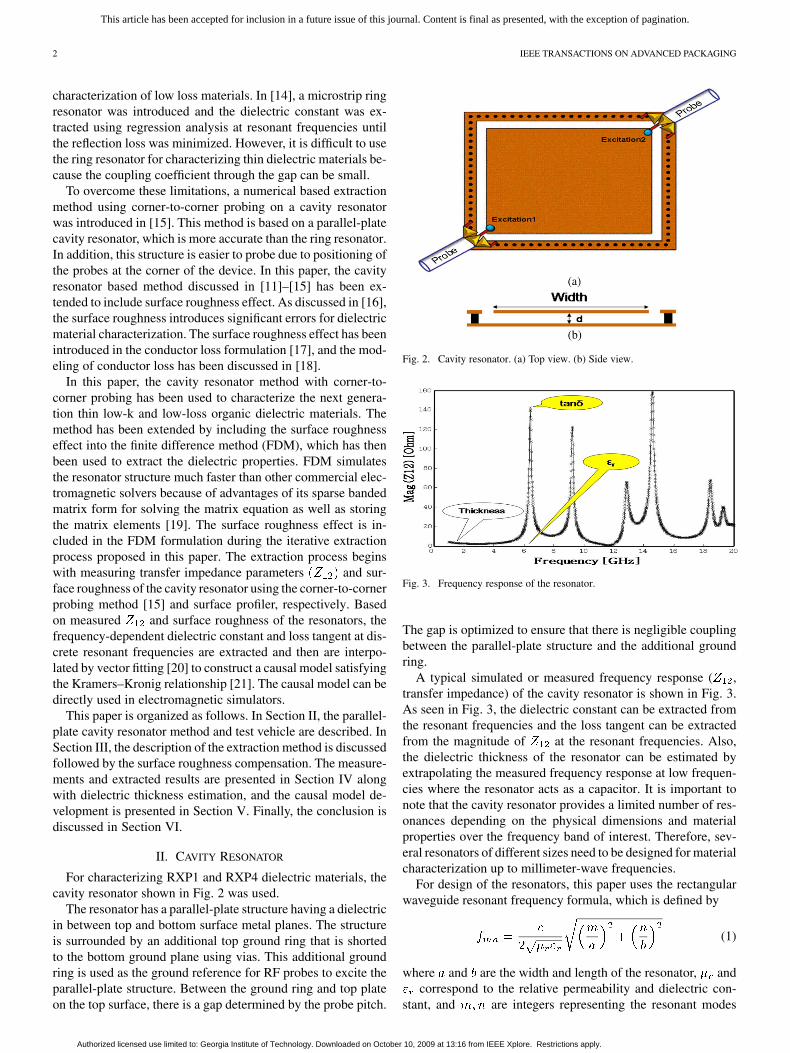
For characterizing RXP1 and RXP4 dielectric materials, thecavity resonator shown in Fig. 2 was used.
The resonator has a parallel-plate structure having a dielectricin between top and bottom surface metal planes. The structureis surrounded by an additional top ground ring that is shortedto the bottom ground plane using vias. This additional groundring is used as the ground reference for RF probes to excite theparallel-plate structure. Between the ground ring and top plateon the top surface, there is a gap determined by the probe pitch.
Fig. 2. Cavity resonator. (a) Top view. (b) Side view.
Fig. 3. Frequency response of the resonator.
The gap is optimized to ensure that there is negligible couplingbetween the parallel-plate structure and the additional groundring.
A typical simulated or measured frequency response ( ,transfer impedance) of the cavity resonator is shown in Fig. 3.As seen in Fig. 3, the dielectric constant can be extracted fromthe resonant frequencies and the loss tangent can be extractedfrom the magnitude of at the resonant frequencies. Also,the dielectric thickness of the resonator can be estimated byextrapolating the measured frequency response at low frequen-cies where the resonator acts as a capacitor. It is important tonote that the cavity resonator provides a limited number of res-onances depending on the physical dimensions and materialproperties over the frequency band of interest. Therefore, sev-eral resonators of different sizes need to be designed for materialcharacterization up to millimeter-wave frequencies.
For design of the resonators, this paper uses the rectangularwaveguide resonant frequency formula, which is defined by
(1)
where and are the width and length of the resonator, andcorrespond to the relative permeability and dielectric con-
stant, and are integers representing the resonant modes
Authorized licensed use limited to: Georgia Institute of Technology. Downloaded on October 10, 2009 at 13:16 from IEEE Xplore. Restrictions apply.

This article has been accepted for inclusion in a future issue of this journal. Content is final as presented, with the exception of pagination.
HWANG et al.: CHARACTERIZATION OF NEXT GENERATION THIN LOW-K AND LOW-LOSS ORGANIC DIELECTRICS 3
TABLE IPHYSICAL DIMENSIONS OF RESONATORS
[22]. However, it is important to note that (1) can be inaccu-rate for characterizing lossy materials.
Based on (1), five cavity resonators were designed for char-acterizing the RXP1 and RXP4 materials. The physical dimen-sions of the resonators are summarized in Table I. A gap of100 m was used for all resonators, which results in negligiblefringing capacitance for both the RXP1 and RXP4 dielectrics.
III. MODELING FOR EXTRACTION
Based on the physical dimensions of the resonator and di-electric material parameters, the resonator needs to be simulatedby using electromagnetic solvers until the simulated response isclose to the measured response at the discrete resonant frequen-cies. This is done by iteratively changing the dielectric param-eters of the material. In this paper, the finite difference method(FDM) has been used and automated to compute the transfer-impedance parameters. The transfer-impedance parame-ters are less sensitive to probe parasitics and hence de-embed-ding is not required.
The FDM formulation has been discussed in detail in [19].In this paper, the formulation has been extended to include thesurface roughness effect. The FDM method replaces the cavityresonator shown in Fig. 2 by a square mesh where the impedance( ) and admittance ( ) of each unit cell in the mesh can becalculated as [23]
(2)
(3)
where is the loss tangent, is the conductivity, is thethickness of the conductor, and and are capacitanceand inductance of the unit cell that can be expressed as
(4a)
(4b)
In the above equations, is the permittivity, is the width ofthe unit cell, and is the thickness of the dielectric. The secondterm in (2) represents the dielectric loss. In (3), the second termrepresents the ac resistance due to skin effect and internal in-ductance while the third term represents the dc resistance.
As the frequency increases, constant conductivity in (3) isno longer valid because the surface roughness significantlydecreases the conductivity at high frequencies where the skin
depth becomes smaller than the surface roughness. Based on[24], the frequency-dependent conductivity can be expressed as
(5)
where is the frequency, is the conductivity at low frequency,and is the root mean square of the surface roughness.
Substituting (5) into (3), the impedance of each unit cell canbe rewritten as
(6)
In the simulation technique used for material characteriza-tion in [15], the extraction process is performed by using a widefrequency range around the resonant frequency. Since the sim-ulation time is directly proportional to the number of frequencypoints, the computational cost can be very high. Therefore, inthis paper a narrowband simulation technique has been used toreduce the computational time.
The correlation process begins with the extraction of resonantfrequencies from the measured response obtained from theS-parameters. The resonant frequencies can be estimated usingthe imaginary parts of poles extracted from measured datawhere the poles can be obtained from vector fitting [20]. How-ever, it is important to note that the extracted resonant frequen-cies may not be the same as the measured frequency points. Forextracting the material parameters accurately, this paper usesthree measured frequency points, namely the frequency at res-onance and two adjacent frequency points. Then, an iterativesimulation is performed until good correlation is obtained at allthe three frequency points. To iteratively compute the materialproperties, Nelder–Mead simplex method [25] was used untilthe least square error between the simulated and measured re-sults is minimum. A flow chart of the iterative extraction processis shown in Fig. 4, and a typical narrowband simulation resultafter convergence is shown in Fig. 5 where the simulated resultslie exactly on top of the measured results.
IV. MEASUREMENTS AND RESULTS
The surface roughness of the conductor was measured usinga Veeco Instruments Sloan DEKTAK 3030 surface profiler. Theprobe of the system travels on the surface of the conductor.Fig. 6 shows the surface roughness measurement results forRXP1 and RXP4 dielectric materials. The horizontal axis is inmicrons, and the vertical axis is in angstroms. The measured sur-face roughness of RXP1 was 0.78 m, and the measured surfaceroughness of RXP4 was 1.03 m, which represent root meansquare (rms) values of the measurement across the surface ofthe cavity resonator.
To illustrate the effect of surface roughness on the conduc-tivity, the frequency-dependent conductivity of copper from 1 to40 GHz for RXP1 and RXP4 is shown in Fig. 7. As shown in the
Authorized licensed use limited to: Georgia Institute of Technology. Downloaded on October 10, 2009 at 13:16 from IEEE Xplore. Restrictions apply.

This article has been accepted for inclusion in a future issue of this journal. Content is final as presented, with the exception of pagination.
4 IEEE TRANSACTIONS ON ADVANCED PACKAGING
Fig. 4. Flow chart of extraction process.
Fig. 5. Correlation result from narrowband simulation.
figure, the skin depth becomes smaller than the surface rough-ness at 7.2 GHz for RXP1 and 4.1 GHz for RXP4 (shown as starin the figure) where the frequency-dependent conductivity be-comes less than half of the original conductivity ( S/m).Above 40 GHz, the effective conductivity approachesS/m.
For the extraction of dielectric constant and loss tangent upto 110 GHz, the frequency range was divided into three partsnamely 1–40 GHz, 40–67 GHz, and 67–110 GHz. The mea-surements were carried out using short-open-load-thru (SOLT)calibration. Up to 40 GHz, six resonators (32.5, 12.5, 9.5 mmfor the RXP1 and RXP4) were measured using Agilent PNA8363B with Cascade GSG-500 air coplanar probes. From 40GHz to 67 GHz, 6.5 mm resonator was measured using AgilentPNA E8361C with GSG-250 air coplanar probes, and AgilentVNA 8510C was used for measurement on a 4.5 mm resonatorfrom 67 GHz to 110 GHz with GSG-250 air coplanar probes.The measured S-parameters were converted into impedance pa-rameters for extracting the dielectric properties. Fig. 8 showsthe corner-to-corner probing, and the measured responsesof resonators on RXP from 1 to 110 GHz are shown in Fig. 9.
Using the method proposed in this paper, the dielectric con-stant and loss tangent were successfully extracted at all the res-onant frequencies; Fig. 10 shows one of the high frequency re-sults at 23.55 GHz where the measured and simulated results aresuperimposed, demonstrating correlation. The extracted RXP1
Fig. 6. Surface roughness measurement. (a) RXP1 measurement. (b) RXP4measurement.
Fig. 7. Frequency-dependent conductivity for RXP1 and RXP4.
results are shown in Fig. 11, and the extracted RXP4 results areshown in Fig. 12; both over a frequency band from 2 GHz to110 GHz. It should be noted that the results contain all of theextracted results from the five designed resonators.
As shown in Fig. 9(c) and (d), the measured response from 40to 110 GHz exhibits peaks at resonant frequencies that are notas sharp as from 1–40 GHz. Although these non-sharp peaks donot affect the extraction of dielectric constant, it can introduceerror in the loss tangent extraction. To improve accuracy of losstangent extraction from 40 to 110 GHz, a full wave simulator[26] was used. It is important to note that the extraction processin Fig. 4 has not changed.
Authorized licensed use limited to: Georgia Institute of Technology. Downloaded on October 10, 2009 at 13:16 from IEEE Xplore. Restrictions apply.

This article has been accepted for inclusion in a future issue of this journal. Content is final as presented, with the exception of pagination.
HWANG et al.: CHARACTERIZATION OF NEXT GENERATION THIN LOW-K AND LOW-LOSS ORGANIC DIELECTRICS 5
Fig. 8. Corner-to-corner probing.
Fig. 9. Measured transfer impedance �� �. (a) 32.5 mm resonator with RXP1.(b) 9.5 mm resonator with RXP1. (c) 6.5 mm resonator with RXP4. (d) 4.5 mmresonator with RXP4.
Fig. 10. Correlation result at 23.55 GHz.
For verifying extraction process, material properties ex-tracted around 1 GHz from the four resonators are summarizedin Table II. The results show very little deviation, demonstratingaccuracy of the extracted results.
To illustrate the effect of surface roughness on the dielec-tric constant and loss tangent extraction, the characterization
Fig. 11. RXP1 extracted results. (a) Dielectric constant. (b) Loss tangent.
results without and with the surface roughness effect on RXP1are shown in Fig. 13. As seen in Fig. 13(a), there are small dif-ferences for the dielectric constant in both cases. However, theeffect of surface roughness on the extracted loss tangent can belarge, as shown in Fig. 13(b). Therefore, the surface roughnessfrom the conductor mainly affects the loss tangent during theextraction process.
Using the proposed method, the dielectric thickness can beextracted using the response at low frequencies. The extractedthickness of RXP1 and RXP4 were 115.5 m and 19.2 m asshown in Fig. 14(a) and (b), respectively. Unlike material pa-rameters extraction, the thickness can be measured by cross sec-tioning where the resonator can be cut in half to examine thethickness, as shown in Fig. 14(c) and (d). The extracted thick-ness is within the range of the measured result from the crosssectioning. This also demonstrates the efficiency of the pro-posed method for estimating the dielectric thickness, which isa critical parameter since it affects the loss tangent extraction.
V. CAUSAL MODEL DEVELOPMENT
The extracted dielectric constant and loss tangent may violatecausality because of measurement inaccuracies. Bode’s integralrelationship, which satisfies causality [21], requires a relation-ship between the real and imaginary parts of any complex func-tion. A typical model that satisfies Bode’s integral relationship isthe Debye model, which can be used in electromagnetic solvers
Authorized licensed use limited to: Georgia Institute of Technology. Downloaded on October 10, 2009 at 13:16 from IEEE Xplore. Restrictions apply.

This article has been accepted for inclusion in a future issue of this journal. Content is final as presented, with the exception of pagination.
6 IEEE TRANSACTIONS ON ADVANCED PACKAGING
Fig. 12. RXP4 extracted results. (a) Dielectric constant. (b) Loss tangent.
TABLE IIEXTRACTED MATERIAL PROPERTIES AT 1 GHZ
to obtain causal results. The Debye model has been constructedby using vector fitting method in this paper [20].
Based on the extracted frequency-dependent dielectric con-stant and loss tangent at discrete frequencies, vector fittingmethod can be used to create a state space representation. Thisresults in a Debye model of the form
(7a)
(7b)
Fig. 13. Surface roughness effect on RXP1. (a) Dielectric constant. (b) Losstangent.
Fig. 14. Thickness estimation and measurement. (a) Correlation for RXP1. (b)Correlation for RXP4. (c) Measured cross-section for RXP1. (d) Measured crosssection for RXP4.
where is the frequency, and are the real part ofcomplex permittivity and loss tangent at very high frequency,
and are poles with negative real parts, and and areresidues with positive real parts, respectively. To ensure the re-sulting Debye model can be realizable using an RC network, theorder of approximation in vector fitting was limited to two polesfor obtaining positive residue results since higher orders maylead to negative residues. Using the constructed causal models,
Authorized licensed use limited to: Georgia Institute of Technology. Downloaded on October 10, 2009 at 13:16 from IEEE Xplore. Restrictions apply.

This article has been accepted for inclusion in a future issue of this journal. Content is final as presented, with the exception of pagination.
HWANG et al.: CHARACTERIZATION OF NEXT GENERATION THIN LOW-K AND LOW-LOSS ORGANIC DIELECTRICS 7
Fig. 15. Causal model with extracted results. (a) Dielectric constant. (b) Losstangent.
the dielectric constant and loss tangent of RXP1 and RXP4 werecomputed at all the frequencies, as shown in Fig. 15.
The dielectric constant in the causal model shows a variationless than 3% over the 110 GHz band for RXP1, and the RXP4result has a variation of less than 2% over the 110 GHz band.The loss tangent has values between 0.0037–0.006 for RXP1,and 0.004–0.0053 for RXP4 in the frequency range from 1–110GHz.
VI. CONCLUSION
The dielectric properties of next generation thin low-k andlow-loss dielectric materials were successfully characterizedfrom 1 GHz to 110 GHz. The extracted dielectric constantof RXP1 was with loss tangentup to 110 GHz. For RXP4, the extracted dielectric constantwas with loss tangent up to110 GHz. A causal model for the dielectric parameters wassuccessfully constructed from the extracted results, whichincludes the surface roughness effect. This paper also presentedan implementation of the surface roughness effect into the finitedifference method and full wave simulator so that more reliablecorrelation results at high frequencies can be achieved. Based
on the results, RXP materials can be used in RF applicationssince they have stable and good high frequency properties.
REFERENCES
[1] W. Yun, V. Sundaram, and M. Swaminathan, “High-Q embedded pas-sives on large panel multilayer liquid crystalline polymer-based sub-strate,” IEEE Trans. Adv. Packag., vol. 30, no. 3, pp. 580–591, Aug.2007.
[2] M. V. Jacob et al., “Temperature dependence of complex permittivityof planar microwave materials,” in Proc. Asia-Pacific Microwave Conf.,Dec. 2006, vol. 3, no. 1, pp. 1453–1456.
[3] W. Yun et al., “3D integration and characterization of high Q passiveson multilayer liquid crystalline polymer (M-LCP) based substrate,” inProc. Asia-Pacific Microwave Conf., Dec. 2005, vol. 1, no. 4–7, pp. 4–.
[4] S. Dalmia et al., “Liquid crystalline polymer (LCP) based lumped-element bandpass filters for multiple wireless applications,” in IEEEMTT-S Int. Microwave Symp. Dig., Jun. 2004, vol. 3, no. 6–11, pp.1991–1994.
[5] D. C. Thompson, O. Tantot, and H. Jallageas, “Characterization ofliquid crystal polymer (LCP) material and transmission lines on LCPsubstrates from 30 to 110 GHz,” IEEE Trans. Microwave Theory Tech.,vol. 52, no. 4, pp. 1343–1352, Apr. 2004.
[6] D. Thompson et al., “RF characteristics of thin film liquid crystalpolymer (LCP) packages for RF MEMS and MMIC integration,” inMicrowave Symp. Dig., Jun. 2005, no. 12–17, p. 4.
[7] D. Athreya et al., “Ultra high Q embedded inductors in highly miniatur-ized family of low loss organic substrates,” in Proc. Electron. Compon.Technol. Conf., 2008, pp. 2073–2080.
[8] G. Krishnan et al., “High performance organic dielectrics and highdensity substrates for next generation system on a package (SOP)technology,” in Proc. Electron. Compon. Technol. Conf., 2008, pp.2101–2104.
[9] V. Sundaram et al., “Super high density two metal layer ultra-thin or-ganic substrates for next generation system-on-package (SOP), SiP andultra-fine pitch flip-chip packages,” presented at the Pan Pacific Micro-electron. Symp., HI, 2009.
[10] A. Deutsch et al., “Extraction of � ��� and ��� ���� for printed circuitboard insulators up to 30 GHz using the short-pulse propagation tech-nique,” IEEE Trans. Adv. Packag., vol. 28, no. 1, pp. 4–12, Feb. 2005.
[11] J. Baker-Jarvis et al., “Dielectric characterization of low-loss materialsa comparison of techniques,” IEEE Trans. Dielect. Elect. Insul., vol. 5,no. 4, pp. 571–577, Aug. 1998.
[12] X. Fang et al., “A tunable split resonator method for nondestructivepermittivity characterization,” IEEE Trans. Instrum. Meas., vol. 53, no.6, pp. 1473–1478, Dec. 2004.
[13] L. S. Napoli and J. J. Hughes, “A simple technique for the accuratedetermination of the microwave dielectric constant for microwave in-tegrated circuit substrates,” IEEE Trans. Microwave Theory Tech., vol.19, no. 7, pp. 664–665, Jul. 1971.
[14] X. Fang et al., “Dielectric constant characterization using a numericalmethod for the microstrip ring resonator,” Microwave Opt. Technol.Lett., vol. 41, no. 1, pp. 14–17, Apr. 2004.
[15] A. E. Engin et al., “Dielectric constant and loss tangent characterizationof thin high-k dielectric using corner-to-corner plane probing,” in Proc.IEEE Electrical Performance Electron. Packag., 2006, pp. 29–32.
[16] A. Deutsch et al., “Accuracy of dielectric constant measurement usingthe full-sheet-resonance technique,” in Proc. IEEE Electrical Perfor-mance of Electron. Packag., 2002, pp. 311–314.
[17] H. Braunisch et al., “Off-chip rough-metal-surface propagation lossmodeling and correlation with measurements,” in Proc. Electron.Compon. Technol. Conf., 2007, pp. 785–791.
[18] X. Chen, “EM modeling of microstrip conductor losses including sur-face roughness effect,” IEEE Microw. Wireless Comp. Lett., vol. 17, no.2, pp. 94–96, Feb. 2007.
[19] A. E. Engin, K. Bharath, and M. Swaminathan, “Multilayered finite-difference method (MFDM) for modeling of package and printed cir-cuit board planes,” IEEE Trans. Electromagn. Compat., vol. 49, no. 2,pp. 441–447, May 2007.
[20] B. Gustavsen and A. Semlyen, “Rational approximation of frequencydomain responses by vector fitting,” IEEE Trans. Power Del., vol. 14,no. 3, pp. 1052–1061, Jul. 1999.
[21] H. W. Bode, Network Analysis and Feedback Amplifier Design. NewYork: Van Nostrand, 1945.
[22] D. M. Pozar, Microwave Engineering. New York: Wiley, 2005.
Authorized licensed use limited to: Georgia Institute of Technology. Downloaded on October 10, 2009 at 13:16 from IEEE Xplore. Restrictions apply.

This article has been accepted for inclusion in a future issue of this journal. Content is final as presented, with the exception of pagination.
8 IEEE TRANSACTIONS ON ADVANCED PACKAGING
[23] M. Swaminathan and A. E. Engin, Power Integrity Modeling and De-sign for Semiconductors and Systems. Englewood Cliffs, NJ: Pren-tice-Hall, 2007, pp. 117–122.
[24] S. Groiss, “Numerische Analyse Verlustbehafter Hohlraumres-onatoren,” Ph.D. dissertation, Technische Univ. Graz, Graz, Austria,1996.
[25] J. C. Lagarias et al., “Convergence properties of the Nelder-Mead sim-plex method in low dimensions,” SIAM J. Optim., vol. 9, no. 1, pp.112–147, 1998.
[26] Sonnet Suites V11. Syracuse, NY.
Seunghyun Hwang received the B.S. degree inelectrical engineering from the University of Wash-ington, Seattle, in 2007, and the M.S. degree fromthe Georgia Institute of Technology, Atlanta, in2009, where he is pursuing the Ph.D. degree in theSchool of Electrical and Computer Engineering.
His research interests include system on package inRF passive design, material characterization on newdeveloping substrate materials, and the design of RFfront-end module.
Sunghwan Min (M’00) was born in Pohang, Korea,in 1970. He received the B.S. degree in electronic en-gineering from Hanyang University, Ansan, Korea,in 1996 and the M.S. and Ph.D. degrees in electricaland computer engineering from Georgia Institute ofTechnology, Atlanta, in 2001 and 2004, respectively.
From 2004 to 2005, he was with the Package De-velopment Team of System LSI Division at SamsungElectronics, Kiheung, Korea, where he was involvedin package design, signal and power integrity, andEMI of mobile phones, digital TV, and multimedia
products. From 2005 to 2008, he was with Jacket Micro Devices, Atlanta, GA,where he was involved in design and integration of filters and front-end mod-ules into a package, process control monitoring, and characterization of sub-strate dielectrics and packaging materials. He is currently a research faculty atGeorgia Institute of Technology. His research interests are in design, electro-magnetic modeling, signal and power integrity, characterization of digital, RF,millimeter-wave, and mixed-signal packages and systems.
Madhavan Swaminathan (M’95–SM’98–F’06) re-ceived the B.E. degree in electronics and communi-cation from the University of Madras, India, and theM.S. and Ph.D. degrees in electrical engineering fromSyracuse University, Syracuse, NY.
He is currently the Joseph M. Pettit Professor inElectronics in the School of Electrical and Com-puter Engineering, Georgia Institute of Technology,Atlanta, the Director of the SRC Interconnect andPackaging Center, and directs the design activities atthe Packaging Research Center. He was the Deputy
Director of the Packaging Research Center, Georgia Institute of Technology,from 2004 to 2008. He is the co-founder of Jacket Micro Devices, a companyspecializing in integrated devices and modules for wireless applications and thefounder of E-System Design, an EDA company focusing on CAD developmentfor integrated microsystems. Prior to joining Georgia Institute of Technology,he was with the Advanced Packaging Laboratory at IBM working on packagingfor super computers. He has over 300 publications in refereed journals andconferences, has co-authored three book chapters, has 17 issued patents, andhas several patents pending. He is also the principal author of the book PowerIntegrity Modeling and Design for Semiconductors and Systems (EnglewoodCliffs, NJ: Prentice-Hall, 2007) and co-editor of the book Introduction toSystem on Package (SOP) (New York: McGraw-Hill, 2008). His researchinterests are in mixed signal micro-system and nano-system integration withemphasis on design, CAD, electrical test and new architectures.
Dr. Swaminathan reached the second invention plateau while at IBM. Heserved as the Co-Chair for the 1998 and 1999 IEEE Topical Meeting on Elec-trical Performance of Electronic Packaging (EPEP), served as the Technical andGeneral Chair for the IMAPS Next Generation IC & Package Design Workshop,serves as the Chair of TC-12, the Technical Committee on Electrical Design,
Modeling and Simulation within the IEEE CPMT society and was the Co-Chairfor the 2001 IEEE Future Directions in IC and Package Design Workshop. Heis the co-founder of the IMAPS Next Generation IC & Package Design Work-shop and the IEEE Future Directions in IC and Package Design Workshop.He also serves on the technical program committees of EPEP, Signal Propa-gation on Interconnects workshop, Solid State Devices and Materials Confer-ence (SSDM), Electronic Components and Technology Conference (ECTC),and International Symposium on Quality Electronic Design (ISQED). He is thefounder of Electrical Design of Advanced Packaging and Systems, a Signal In-tegrity Symposium in the Asian region. He has been a guest editor for the IEEETRANSACTIONS ON ADVANCED PACKAGING and the IEEE TRANSACTIONS ON
MICROWAVE THEORY AND TECHNIQUES. He was the Associate Editor of theIEEE TRANSACTIONS ON COMPONENTS AND PACKAGING TECHNOLOGIES. Hecurrently serves on the CAD committee of Microwave Theory and Techniques.He is the recipient of the 2002 Outstanding Graduate Research Advisor Awardfrom the School of Electrical and Computer Engineering, Georgia Institute ofTechnology and the 2003 Outstanding Faculty Leadership Award for the men-toring of graduate research assistants from Georgia Institute of Technology. Heis also the recipient of the 2003 Presidential Special Recognition Award fromIEEE CPMT Society for his leadership of TC-12 and the IBM Faculty Award in2004 and 2005. He has also served as the co-author and advisor for a number ofoutstanding student paper awards at EPEP’08, EPEP’00, EPEP’02, EPEP’03,EPEP’04, EPEP’08, ECTC’98, ECTC’08, APMC’05 and the 1997 IMAPS Ed-ucation Award. Dr. Swaminathan is the recipient of the Shri. Mukhopadyaybest paper award at the International Conference on Electromagnetic Interfer-ence and Compatibility (INCEMIC), Chennai, India, 2003, the 2004 best paperaward in the IEEE Transactions on Advanced Packaging, the 2004 commend-able paper award in the IEEE Transactions on Advanced Packaging and thebest poster paper award at ECTC’04 and ’06. In 2007, Dr. Swaminathan wasrecognized for his research through the Technical Excellence Award given bySemiconductor Research Corporation (SRC) and Global Research Corporation(GRC).
Venkatesan Venkatakrishnan received the B.S.degree in physics from Madras University, Madras,India, the M.S. degree in applied electronics fromRegional Engineering College, Trichy, India, and theM.Tech. degree in microwave electronics from DelhiUniversity, Delhi, India, in 1984, 1986, and 1988,respectively.
He joined SAMEER-Centre for Electromagnetics,Madras, in 1988 as Scientist and has been with theinstitution since then. He has been working in theareas of electromagnetics, EMI/EMC, and antennas.
He was deputed to work as Guest Scientist for a brief period in 1991, in the“fields and interference meterology division” of NIST, Boulder, CO, under theUNDP fellowship program in the area of EMI/EMC. He has also worked for aperiod of four months in the year 2007 at Packaging Research Center, GeorgiaInstitute of Technology, Atlanta, in the area of material characterization. Hiscurrent research areas include analysis, design and development of ultra wideband aperture antennas and material characterization involving low loss ultrathin packaging materials.
Hunter Chan received the B.S. degree in elec-trical engineering from California State University,Fresno, in 1982 and the M.S. degree in electricalengineering from Georgia Institute of Technology,Atlanta, in 1984.
His focus as a Research Engineer at Georgia Insti-tute of Technology Electronics Packaging ResearchCenter (PRC) is in the area of multilayer organicsubstrates, high density wiring, microvia processesand SOP substrate integration. He is the PRC projectleader for the Low Loss/Thin Core Substrate Project
in the Embedded Actives and Passives (EMAP) Consortium, as well as theproject leader for the membership project on “ultra-fine lines on emergingdielectrics for next generation microprocessor package substrate.” He has morethan 20 years industrial experience in High Density Multiwire and PWBs withlased microvias technology, and embedded resistors for high speed digitalapplications. He has one U.S. patent pending.
Mr. Chan is a member of Tau Beta Pi and Etta Kappa Nu Honor Societies inEngineering.
Authorized licensed use limited to: Georgia Institute of Technology. Downloaded on October 10, 2009 at 13:16 from IEEE Xplore. Restrictions apply.

This article has been accepted for inclusion in a future issue of this journal. Content is final as presented, with the exception of pagination.
HWANG et al.: CHARACTERIZATION OF NEXT GENERATION THIN LOW-K AND LOW-LOSS ORGANIC DIELECTRICS 9
Fuhan Liu is Program Manager of Advanced Sub-strate Research with the Packaging Research Center,Georgia Institue of Technology, Atlanta. He iscurrently focused on the R&D of system-on-package(SOP) integrations, thin and high density packagingtechnologies, embedded actives, passives and opto-electronics, low Dk and low Df materials, processdevelopment, and high performance prototypefabrications. He has been working in the area formore than 10 years.
Venky Sundaram received the Ph.D. degree in ma-terials science and engineering and the M.S. degreein ceramic and materials engineering from GeorgiaInstitute of Technology, Atlanta, and the B.S. degreein metallurgical engineering from Indian Institute ofTechnology, Bombay.
He is the Director of Research at the Georgia Insti-tute of Technology Packaging Research Center, At-lanta, and a Senior Research Faculty in the School ofElectrical and Computer Engineering. He has leader-ship responsibility for SOP (System-on-a-Package)
Integration Research and Several Large Industry Consortia and Contract Pro-grams requiring the establishment of center wide research programs develop-ment and collaborations with global industry and U.S./international universi-ties and research groups. His research expertise includes SOP integration R&D,next generation substrate and assembly technologies and multi-mega functionmodule technologies for electronic and bio-electronic systems. He has morethan 12 years experience in advanced packaging technologies including SOP,SiP, high-density microvia substrates, thin film wiring, and embedded actives/passives. He is the co-founder of Jacket Micro Devices, a RF module tech-nology start-up and frequently consults for semiconductor and packaging com-panies world-wide. He has more than 75 publications, five U.S. and internationalpatents, and multiple patents pending in SOP substrate technology and RF/dig-ital packaging.
Dr. Sundaram is a member of the High Density Substrate Technical Com-mittee (TC-6) of IEEE-CPMT Society.
Scott Kennedy is currently an applications develop-ment manager for Rogers Corporation. He has beenwith Rogers for nine years and is responsible forthe technical development of Ultralam® 3000 LiquidCrystal Polymer and Syron™ 7000 circuit laminatesystems. Scott also developed suitable materialsfor the microelectronic packaging markets. Scottholds four US patents and has several applicationspending. Scott has authored or co-authored fourindustry articles. Scott has a B.S. is chemical andmaterials engineering and a M.S. in polymer science.
Dirk Baars received the B.S. degree in chemicalengineering and the M.S. degree in chemical en-gineering practice, both from the MassachusettsInstitute of Technology, Cambridge.
He is the Director of the Advanced MaterialsGroup, Rogers Corporation Lurie R&D Center,Rogers, CT. His group develops new materialsfor high frequency, high speed, and high densityelectrical interconnect applications. Previous tohis current assignment, he was Vice President andGeneral Manager of Rogers’ Moldable Composites
Division. He holds six U.S. patents in diverse materials fields.
Benjamin Lacroix received the Ph.D. degree in elec-trical and telecommunications engineering from theUniversity of Limoges, France, in 2008. As a Ph.D.student with the XLIM Research Institute, he devel-oped fast miniature RF MEMS switched capacitorsand high-speed reconfigurable low-loss DMTL (dis-tributed MEMS transmission lines) phase shifters.
He joined the MiRCTech Research Group, GeorgiaInstitute of Technology, Atlanta, in December 2008,as a Postdoctoral Fellow. His current research is fo-cused on reconfigurable microwave filters using fer-
roelectric BST capacitors. He also works on RF MEMS tunable devices andreliability of RF MEMS switches.
Yuan Li received the B.S. degree in automaticcontrol from Northwestern Polytechnical University,Xi’an, China, the M.S. degree in electrical engi-neering from the Georgia Institute of Technology,Atlanta, in 2004, where he is currently pursuing thePh.D. degree in electrical and computer engineering.
He was an Electronic and RF Engineer in in-dustry. He is currently a Research Assistant inthe MiRCTECH Research Group, Georgia Elec-tronic Design Center (GEDC), Georgia Institute ofTechnology. His research interests include the de-
velopment and characterization of micromachined circuits for millimeter-waveand terahertz applications, packaging technology for millimeter-wave systems,and passive and active circuits for wireless systems.
John Papapolymerou (SM’04) received theB.S.E.E. degree from the National Technical Uni-versity of Athens, Athens, Greece, in 1993, and theM.S.E.E. and Ph.D. degrees from the University ofMichigan, Ann Arbor, in 1994 and 1999, respec-tively.
From 1999 to 2001, he was an Assistant Professorwith the Department of Electrical and ComputerEngineering, University of Arizona, Tucson, andduring the summers of 2000 and 2003, he was aVisiting Professor at the University of Limoges,
France. From 2001 to 2005 he was an Assistant Professor at the School ofElectrical and Computer Engineering, Georgia Institute of Technology, wherehe is currently an Associate Professor. He has authored or coauthored over 250publications in peer-reviewed journals and conferences. His research interestsinclude the implementation of micromachining techniques and MEMS devicesin microwave, millimeter-wave and THz circuits and the development of bothpassive and active planar circuits on semiconductor (Si/SiGe, GaAs) andorganic substrates (liquid crystal polymer-LCP, LTCC) for System-on-a-Chip(SOC)/System-on-a-Package (SOP) RF front ends.
Dr. Papapolymerou is the Chair for Commission D of the U.S. NationalCommittee of URSI. He is Associate Editor for the IEEE MICROWAVE AND
WIRELESS COMPONENT LETTERS and the IEEE TRANSACTIONS ON ANTENNAS
AND PROPAGATION. During 2004, he was the Chair of the IEEE MTT/APAtlanta Chapter. He was the recipient of the 2009 IEEE MTT-S OutstandingYoung Engineer Award, the 2004 Army Research Office (ARO) Young Inves-tigator Award, the 2002 National Science Foundation (NSF) CAREER award,the best paper award at the 3rd IEEE International Conference on Microwaveand Millimeter-Wave Technology (ICMMT2002), Beijing, China and the 1997Outstanding Graduate Student Instructional Assistant Award presented bythe American Society for Engineering Education (ASEE), The University ofMichigan Chapter. His students have also been recipients of several awardsincluding the Best Student Paper Award presented at the 2004 IEEE TopicalMeeting on Silicon Monolithic Integrated Circuits in RF Systems, the 2007IEEE MTT-S Graduate Fellowship, and the 2007/2008 and 2008/2009 IEEEMTT-S Undergraduate Scholarship/Fellowship.
Authorized licensed use limited to: Georgia Institute of Technology. Downloaded on October 10, 2009 at 13:16 from IEEE Xplore. Restrictions apply.