
Characterization and Modeling of Ceramic Capacitor Losses ...
72
Characterization and Modeling of Ceramic Capacitor Losses in High Density Power Converters Samantha Coday Electrical Engineering and Computer Sciences University of California at Berkeley Technical Report No. UCB/EECS-2019-34 http://www2.eecs.berkeley.edu/Pubs/TechRpts/2019/EECS-2019-34.html May 14, 2019
Transcript of Characterization and Modeling of Ceramic Capacitor Losses ...

Characterization and Modeling of Ceramic Capacitor Lossesin High Density Power Converters
Samantha Coday
Electrical Engineering and Computer SciencesUniversity of California at Berkeley
Technical Report No. UCB/EECS-2019-34http://www2.eecs.berkeley.edu/Pubs/TechRpts/2019/EECS-2019-34.html
May 14, 2019

Copyright © 2019, by the author(s).All rights reserved.
Permission to make digital or hard copies of all or part of this work forpersonal or classroom use is granted without fee provided that copies arenot made or distributed for profit or commercial advantage and that copiesbear this notice and the full citation on the first page. To copy otherwise, torepublish, to post on servers or to redistribute to lists, requires prior specificpermission.

Characterization and Modeling of Ceramic Capacitor Losses in High DensityPower Converters
by
Samantha Nicole Coday
A thesis submitted in partial satisfaction of the
requirements for the degree of
Master of Science
in
Engineering - Electrical Engineering and Computer Sciences
in the
Graduate Division
of the
University of California, Berkeley
Committee in charge:
Prof. Robert Pilawa-Podgurski, ChairProf. Seth SandersProf. Scott Moura
Spring 2019

Characterization and Modeling of Ceramic Capacitor Losses in High DensityPower Converters
Copyright 2019by
Samantha Nicole Coday

1
Abstract
Characterization and Modeling of Ceramic Capacitor Losses in High Density PowerConverters
by
Samantha Nicole Coday
Master of Science in Engineering - Electrical Engineering and Computer Sciences
University of California, Berkeley
Prof. Robert Pilawa-Podgurski, Chair
Ceramic capacitors offer reliable and dense energy storage in power conversion applica-tions. However, to effectively incorporate these devices in a design, it is important to havean accurate model of losses for the conditions under which the devices will be used. Smallsignal loss parameters at low bias voltage are frequently provided by the manufacturer, butthe correlation between these data and losses exhibited under realistic large signal excitationhas not been explored in detail. This work aims to provide a method for measuring ca-pacitor losses under realistic operating conditions, using a calorimetric approach to providean accurate measurement of losses under large signal excitation. Specifically this work willinvestigate the effect of high voltage bias and varying AC excitation on losses. This workconcludes with a proposed loss model which encompasses operation of large signal excitationover varying frequencies and DC biases.

i
For Nana
Mostest

ii
Contents
Contents ii
List of Figures iv
List of Tables vi
1 Introduction 1
2 Background on Multilayer Ceramic Capacitors 32.1 Operating Conditions of Multilayer Ceramic Capacitors . . . . . . . . . . . . 72.2 Case Study: Flying Capacitor Multilevel Inverter . . . . . . . . . . . . . . . 8
3 Comparison of Measurement Techniques 123.1 Electrical Characterization Methods . . . . . . . . . . . . . . . . . . . . . . . 123.2 Calorimetric Characterization Comparison . . . . . . . . . . . . . . . . . . . 133.3 Calorimetric Theory . . . . . . . . . . . . . . . . . . . . . . . . . . . . . . . 14
4 Calorimetric Study 164.1 Theory and Design of Electrical Excitation . . . . . . . . . . . . . . . . . . . 174.2 Calorimetric Setup . . . . . . . . . . . . . . . . . . . . . . . . . . . . . . . . 194.3 Calibration Methods . . . . . . . . . . . . . . . . . . . . . . . . . . . . . . . 204.4 Calorimetric Testing Procedure . . . . . . . . . . . . . . . . . . . . . . . . . 204.5 Measurement Error Analysis . . . . . . . . . . . . . . . . . . . . . . . . . . . 21
5 Experimental Results 245.1 DC Bias Calorimetric Results . . . . . . . . . . . . . . . . . . . . . . . . . . 255.2 AC Amplitude Experimental Results . . . . . . . . . . . . . . . . . . . . . . 295.3 ESR Dependence on Temperature . . . . . . . . . . . . . . . . . . . . . . . . 32
6 Comparison to Low Frequency Electrical Measurements 356.1 Electrical Setup . . . . . . . . . . . . . . . . . . . . . . . . . . . . . . . . . . 356.2 DC Bias Results . . . . . . . . . . . . . . . . . . . . . . . . . . . . . . . . . . 36

iii
7 Loss Model 387.1 Model Theory . . . . . . . . . . . . . . . . . . . . . . . . . . . . . . . . . . . 387.2 Application of Model to Case Study . . . . . . . . . . . . . . . . . . . . . . . 43
8 Conclusions 458.1 Future Work . . . . . . . . . . . . . . . . . . . . . . . . . . . . . . . . . . . . 45
Bibliography 47
A Experimental Data 51
B Electrical Excitation Printed Circuit Board 55

iv
List of Figures
1.1 NASA’s More Electric Aircraft X-Plane Concept [1]. . . . . . . . . . . . . . . . 1
2.1 Size comparison of inductor and MLCC with the same energy density storage.Components are not to scale, but are to relative scale for comparison purposes. . 3
2.2 Composition of a basic multilayer ceramic capacitor. . . . . . . . . . . . . . . . 42.3 Standard capacitor model simplified [2]. . . . . . . . . . . . . . . . . . . . . . . 52.4 Impedance and frequency relationship of a Class II MLCC [3]. . . . . . . . . . . 62.5 Change in capacitance with increased DC voltage bias [3]. . . . . . . . . . . . . 72.6 ESR of three Class II MLCCs over a range of frequencies, at 0 V bias small signal
excitation (0.1 VRMS) provided by the manufacturer [3] [4] [5]. . . . . . . . . . . 82.7 Schematic of nine-level FCML from [6]. Voltage and current waveforms of MLCC
in FCML. . . . . . . . . . . . . . . . . . . . . . . . . . . . . . . . . . . . . . . . 92.8 Actual implementation of capacitors in each switching cell. . . . . . . . . . . . . 9
4.1 Electrical excitation circuit and thermal setup for calorimetric testing. . . . . . . 164.2 Picture of electrical excitation PCB mounted on top of beaker with DUT and
stirring setup. . . . . . . . . . . . . . . . . . . . . . . . . . . . . . . . . . . . . . 184.3 MLCC DUT voltage and current measured at 250 kHz (5A/V). . . . . . . . . . 184.4 Calorimetric setup where the beaker is placed in insulation. The entire system is
placed in the temperature chamber and the power is fed through the side of thechamber. . . . . . . . . . . . . . . . . . . . . . . . . . . . . . . . . . . . . . . . . 19
4.5 Calibration of calorimetric setup utilizing precise resistor in place of DUT tocalculate thermal impedance of setup. . . . . . . . . . . . . . . . . . . . . . . . . 21
5.1 TDK X6S, Cap I from Table 5.1, effect of DC bias on ESR. The black starrepresents the small signal ESR from the data sheet [3]. . . . . . . . . . . . . . . 25
5.2 Knowles X7R, Cap II from Table 5.1, effect of DC bias on ESR. The black starrepresents the small signal ESR from the data sheet [4]. . . . . . . . . . . . . . . 26
5.3 Kemet X7R, Cap III from Table 5.1, effect of DC bias on ESR. The black starrepresents the small signal ESR from the data sheet [7]. . . . . . . . . . . . . . . 27
5.4 Ceralink, Cap IV from Table 5.1, effect of DC bias on ESR. . . . . . . . . . . . 28

v
5.5 TDK C0G, Cap V from Table 5.1, effect of DC bias on ESR. The black starrepresents the small signal ESR from the data sheet [3]. . . . . . . . . . . . . . . 29
5.6 TDK X6S, Cap I from Table 5.1, effect of AC amplitude on ESR. . . . . . . . . 305.7 Kemet X6R, Cap III from Table 5.1 and TDK X6S, Cap I from Table 5.1 effect
of AC amplitude on ESR. . . . . . . . . . . . . . . . . . . . . . . . . . . . . . . 315.8 TDK X6S, Cap I from Table 5.1 effect of AC amplitude on ESR at multiple bias
points. . . . . . . . . . . . . . . . . . . . . . . . . . . . . . . . . . . . . . . . . . 325.9 Dependence of ESR on operating temperature, shown for Cap I from Table 5.1 [3]. 335.10 ESR dependence on temperature for the operating temperatures of this study [3]. 345.11 TDK X6S, Cap I in Table 5.1, 0 V bias at 125 kHz AC current amplitude effect
on ESR. Shows the normalized data, adjusted for changes in temperature. . . . 34
6.1 Low frequency electrical measurement capacitor testing circuit. . . . . . . . . . 366.2 Low frequency bias dependent ESR results, for TDK X6S MLCC (Cap I in Table
5.1), attained through electrical experimental setup. . . . . . . . . . . . . . . . . 376.3 ESR of three Class II MLCCs over a range of frequencies, which highlights the
increased ESR at lower operating frequencies [3] [4] [5]. . . . . . . . . . . . . . . 37
7.1 ESR and DC bias relationship for TDK X6S, Cap. I from Table 5.1 measured at250 kHz, shown with a linear fit. . . . . . . . . . . . . . . . . . . . . . . . . . . 39
7.2 Capacitance and DC bias relationship for TDK X6S, Cap. I from Table 5.1, withan exponential fit [3]. . . . . . . . . . . . . . . . . . . . . . . . . . . . . . . . . . 40
7.3 Calculated α values from optimization, for tested capacitors, listed in Table 5.1. 417.4 Calculated γ values from optimization, for tested capacitors, listed in Table 5.1. 427.5 Modeled and experimental data compared for TDK X6S, Cap. I in Table 5.1. . . 43
B.1 H-bridge schematic for applying electrical excitation across the DUT. . . . . . . 56B.2 Top layer of PCB. . . . . . . . . . . . . . . . . . . . . . . . . . . . . . . . . . . 57B.3 Inner layer one of the PCB. . . . . . . . . . . . . . . . . . . . . . . . . . . . . . 58B.4 Inner layer two of the PCB. . . . . . . . . . . . . . . . . . . . . . . . . . . . . . 59B.5 Bottom layer of the PCB. . . . . . . . . . . . . . . . . . . . . . . . . . . . . . . 60

vi
List of Tables
1.1 Inverter performance requirements [8]. . . . . . . . . . . . . . . . . . . . . . . . 2
2.1 DC voltage bias on flying capacitors in 1 kV input 9-level FCML buck inverter. 102.2 Operating conditions of flying capacitors in nine-level FCML [6]. . . . . . . . . . 11
4.1 Components used in electrical excitation circuit. . . . . . . . . . . . . . . . . . . 174.2 Devices used in calorimetric setup. . . . . . . . . . . . . . . . . . . . . . . . . . 20
5.1 Experimentally evaluated capacitors. . . . . . . . . . . . . . . . . . . . . . . . . 24
6.1 Devices used in low frequency electrical setup. . . . . . . . . . . . . . . . . . . . 35
7.1 Adjusted power loss calculations for case study based on modeled ESR. . . . . . 44
A.1 DC bias characteristic data of TDK X6S, Cap I from Table 5.1. . . . . . . . . . 51A.2 DC bias characteristic data of Knowles X7R, Cap II from Table 5.1. . . . . . . . 52A.3 DC bias characteristic data of Kemet X7R, Cap III from Table 5.1. . . . . . . . 52A.4 DC bias characteristic data of Ceralink MLCC, Cap IV from Table 5.1. . . . . . 53A.5 DC bias characteristic data of TDK C0G, Cap V from Table 5.1. . . . . . . . . 53A.6 AC amplitude characteristic data of TDK X6S, Cap I from Table 5.1. . . . . . . 54A.7 AC amplitude characteristic data of Kemet X7R, Cap III from Table 5.1. . . . . 54

vii
Acknowledgments
First, I would like to thank my parents. Their love and continual support has helped methrough every part of this journey. Thank you to my mother for teaching me how to listenand for showing me selfless kindness everyday. Thank you to my father for teaching me thatintelligence is not measured by number of degrees or in paychecks, but instead by the abilityto communicate ideas to anyone you meet. My parents have demonstrated what hard worklooks like for as long as I can remember, and it is because of their example that I have beenable to persevere. I am so appreciative to have parents who believe in me and cheer me onevery day. My only complaint is how far Texas is from California. Thank you, Mom andDad.
I want to thank Chance, for his constant support and encouragement. I am so gratefulfor all of the phone calls, visits, coffees and adventures over the past few years. Thank youfor believing in me even when I didn’t believe in myself. I couldn’t ask for a better bestfriend. I am so excited for our next adventure.
Thank you to the rest of my family, aunts and uncles, cousins and more. Being awayfrom my parents is always hard, but I am so thankful to have family that would house me,let me play with their kids, and support me. There have been some hard times these pasttwo years, but I always knew I had people to call, to eat egg drop soup with or people whowould drive hours just to bring me furniture. I am incredibly blessed to have such a largesupport network.
Thank you to Allison. You are one of the most thoughtful people I know, and I amhonored to be your friend. Your cards, emails and texts always seemed to come at the timeI needed them most. To Joe for always believing in me, I am so grateful I met you six yearsago in the school cafeteria. We have grown and changed so much but I know our friendshipwill always be around. Thank you for all the times you have supported me. I am so excitedto cheer you on as you begin your next adventure.
Thank you to the Pilawa group. I especially want to thank Nathan Pallo from whom Ihave learned so much over these past two years. I have become a better engineer because ofyou. Thank you to the rest of the NASA team: Chris, Tom, Pourya and Joseph, all of whomhave taught me so much. I also want to thank Maggie. How lucky am I that two Texangirls ended up in the same group? Thank you for being the person I tackle grad school with,for all the late nights doing homework and watching the Bachelor. You are a great friend.Thank you to the rest of the Pilawa group. I am grateful to be surrounded by people whoare brilliant and work extremely hard. I continue to learn from all of you everyday.
Lastly, I want to thank Professor Pilawa. I am grateful for every single day since I begangraduate school. I have learned more these past two years than I ever thought possible. Ihave become a better engineer and been surrounded by people who constantly push me tobe better. I am so appreciative to have joined your group. Thank you for the support andencouragement, I am excited for the next degree and project!
Lastly, I would like to thank the NASA Fixed Wing research program through NASAcooperative agreement NASA NNX14AL79A from which this work was supported.

1
Chapter 1
Introduction
NASA’s More Electric Aircraft (MEA) project was developed to prioritize electrificationin our growing age of transportation access. Objectives of this aircraft design can lead toa 80% reduction in NOx emissions, 60% reduction in fuel consumption as well as 71 dBreduction in noise [1]. Fig. 1.1 shows a concept for the X-plane, a hybrid electric solution.
High power specific density of the electric drive train is a limiting factor for enabling MEA,therefore it is necessary to develop lightweight motors with high specific power. One suchmotor [9, 10] uses a 20 pole outer rotor permanent magnet synchronous machine to achievehigh specific power while remaining lightweight. As opposed to typical motor designs, thismotor has low inductance due to its outer rotor configuration. Low inductance requiresadditional filtering on the inverter to reach low total harmonic distortion (THD) on themotor. Additional filtering can increase the size and weight of the system, so instead a nine-level flying capacitor multilevel (FCML) inverter was developed utilizing its inherently lowTHD output and small filter size requirement [6, 11, 12]. Details of this work can be foundin [6], where a peak power of 9.7 kW at 98.6% efficiency was demonstrated. The desired
Figure 1.1: NASA’s More Electric Aircraft X-Plane Concept [1].

CHAPTER 1. INTRODUCTION 2
Table 1.1: Inverter performance requirements [8].
Specific Power (kW/kg) Efficiency (%)
Minimum 12 98Target 19 99Stretch 25 99.5
requirements of this inverter, set by NASA in [8], can be seen in Table 1.1.While [6] demonstrated an inverter reaching the minimum efficiency, original models
of this inverter design anticipated efficiency within the target region, shown in Table 1.1.To reach the target efficiency it is necessary to systematically evaluate the losses of everycomponent within the inverter. The FCML in [6] uses GaN switches and extensive workwas done in [13] to better characterize the dynamic losses of these switches. However, littleprevious work has been done to understand the losses of the capacitors, which are the mainenergy storage element of this converter [14].
Most conventional power converters (i.e. buck, boost, two-level inverters, etc.) primarilyuse capacitors as filtering elements. Filter capacitors are large with low equivalent seriesresistance (ESR) and low losses. Typically, these capacitors contribute negligible amount oflosses to the overall power loss of the converter. In the FCML converters recently proposed,[6, 11, 12, 15–17], to achieve high power density, the capacitors experience high currents andhigh voltage bias, which can yield increased power loss that comprise a non-negligible portionof the total losses. Therefore, this work will investigate how to model and better understandthese losses.
The rest of this thesis will be organized as follows. Chapter 2 provides backgroundinformation on multilayer ceramic capacitors, detailing their operation and losses. Chapter3 explains different characterization techniques, explaining why an oil-based calorimetricapproach was taken. Chapter 4 provides detail of the calorimetric setup used in this study,including careful techniques to reduce the error. Chapter 5 provides a summary of thecalorimetric experimental results, explaining the trends discovered. Chapter 6 provides anelectrical method and results for investigating losses at lower frequencies. Chapter 7 derivesand explains a new model for Class II MLCCs which allows for understanding of lossesat any operating condition. Chapter 7 also returns to the nine-level FCML MEA in [6]to understand how the introduced model effects the expected losses. Finally, Chapter 8concludes the thesis and explains future work.

3
Chapter 2
Background on Multilayer CeramicCapacitors
Multilayer ceramic capacitors (MLCCs) are a key enabling component for high densitypower converters due to their high energy storage capabilities. Commercially available ML-CCs have energy storage densities which are up to three orders of magnitude higher thancommercially available inductors [18]. Fig. 2.1 shows a comparison of an MLCC and aninductor, both of which have the same energy storage, determined by Eqn. 2.1 and Eqn. 2.2respectively.
Ecapacitor =1
2CV 2 (2.1)
Einductor =1
2LI2 (2.2)
This comparison illustrates that utilizing capacitors as the primary energy storage devicein power converters can enable increased converter power density [12, 16, 19, 20]. Recentadvances in hybrid [21] and resonant [22–24] switched capacitor power converters, as well asvarious multilevel topologies [15,25,26] have led to increased focus on capacitor-based power
Figure 2.1: Size comparison of inductor and MLCC with the same energy density storage.Components are not to scale, but are to relative scale for comparison purposes.

CHAPTER 2. BACKGROUND ON MULTILAYER CERAMIC CAPACITORS 4
Terminals
Dielectric Material
Metallic
Electrodes
Figure 2.2: Composition of a basic multilayer ceramic capacitor.
converter architectures, often with MLCCs as the primary energy storage/transfer elements.To fully capitalize on the potential benefits of MLCCs, it is important to understand andmodel their energy storage and loss characteristics.
Capacitor Introduction
MLCCs are composed of several interwoven parallel plates, with a dielectric spacedthroughout, which is shown in Fig. 2.2. Capacitance is defined in Eqn. 2.3 where pa-rameter ε is the electrical permittivity of the dielectric, A is the area of the electrodes andd is the distance between the electrodes [2]. MLCCs offer high capacitance because theinterwoven electrodes decrease the distance between electrodes as well as increasing the areaof the electrodes. Since energy is defined by Eqn. 2.1, the increased capacitance leads to anincreased energy density.
C =εA
d(2.3)

CHAPTER 2. BACKGROUND ON MULTILAYER CERAMIC CAPACITORS 5
LESLC RESR
LESLC
Rleak
Rw
Figure 2.3: Standard capacitor model simplified [2].
MLCC Model
A commonly used capacitor model can be seen in Fig. 2.3. The electrical losses intermination resistance and series resistance of the dielectric are represented by Rw. Theleakage losses are modeled as Rleak. These two resistances can be effectively combined toequal one equivalent series resistance (ESR) [2]. The real losses of the capacitor can beapproximated by Eqn. 2.4.
Ploss = I2rmsRESR (2.4)
The ESR of a MLCC depends on termination resistance, resistance within the dielectric andhysteresis losses. The resistance of the dielectric varies with large voltage swing as well asDC bias and temperature [27]. Note the model also includes a series inductance, LESL whichis due to the inductance of the termination and composition of the MLCC.
Based on the simplified model shown in Fig. 2.3, the series impedance of an MLCCcan be described as the sum of the impedance of the capacitor, equivalent inductance andresistance, shown in Eqn. 2.5.
ZMLCC = jωLESL +1
jωC+RESR (2.5)
The relationship between frequency and magnitude of the impedance is displayed in Fig.2.4. The impedance reaches a minimum at self-resonance. At this point the impedance isequal to the ESR of the MLCC. The self-resonance frequency is defined in Eqn. 2.6.
freson =1
2π√LESLC
(2.6)
MLCC Comparison
Most MLCCs used in power electronics fall into the category of Class I or Class IIcapacitors. Class I MLCC’s dielectrics are composed of paraelectric materials which arestable over temperature and bias. However, Class I MLCCs have lower energy density thanClass II MLCCs [19]. Class II MLCC’s dielectrics are composed of ferroelectric materials,mainly barium titanate, which allow for extremely dense energy storage, due to their high

CHAPTER 2. BACKGROUND ON MULTILAYER CERAMIC CAPACITORS 6
Figure 2.4: Impedance and frequency relationship of a Class II MLCC [3].
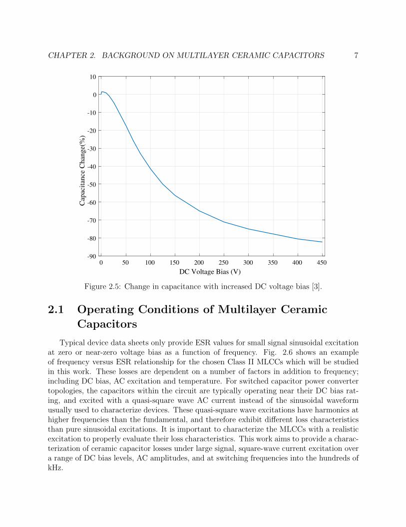
permittivity. However, these ferroelectric materials exhibit changes in permittivity due torealignment of electric dipoles within the material. The change in permittivity results inchanges in the capacitance and ESR of the capacitors [28]. The decrease of capacitance byup to eighty percent at full DC voltage bias, an example of which is shown in Fig. 2.5, isdue to the dipole realignment. The dipole realignment in Class II dielectrics is affected byfour main operating conditions: Frequency, temperature, DC bias and AC amplitude.
Recently released Ceralink MLCCs are composed of a PLZT, lead-lanthanum-zirconate-titanate, dielectric which operates differently than Class I and Class II MLCCs. This di-electric is anti-ferroelectric, implying that as the DC voltage increases the capacitance alsoincreases. This anti-ferroelectric behavior is attractive in hybrid switched capacitor topolo-gies where high capacitance is often desired under high DC bias. Prior work characterized thelosses of Ceralink capacitors at low frequencies and found that while the DC bias capacitancecharacteristics were favorable, the losses were greater than anticipated [27].
CHAPTER 2. BACKGROUND ON MULTILAYER CERAMIC CAPACITORS 7
0 50 100 150 200 250 300 350 400 450
DC Voltage Bias (V)
-90
-80
-70
-60
-50
-40
-30
-20
-10
0
10C
apac
itan
ce C
han
ge(
%)
Figure 2.5: Change in capacitance with increased DC voltage bias [3].
2.1 Operating Conditions of Multilayer Ceramic
Capacitors
Typical device data sheets only provide ESR values for small signal sinusoidal excitationat zero or near-zero voltage bias as a function of frequency. Fig. 2.6 shows an exampleof frequency versus ESR relationship for the chosen Class II MLCCs which will be studiedin this work. These losses are dependent on a number of factors in addition to frequency;including DC bias, AC excitation and temperature. For switched capacitor power convertertopologies, the capacitors within the circuit are typically operating near their DC bias rat-ing, and excited with a quasi-square wave AC current instead of the sinusoidal waveformusually used to characterize devices. These quasi-square wave excitations have harmonics athigher frequencies than the fundamental, and therefore exhibit different loss characteristicsthan pure sinusoidal excitations. It is important to characterize the MLCCs with a realisticexcitation to properly evaluate their loss characteristics. This work aims to provide a charac-terization of ceramic capacitor losses under large signal, square-wave current excitation overa range of DC bias levels, AC amplitudes, and at switching frequencies into the hundreds ofkHz.

CHAPTER 2. BACKGROUND ON MULTILAYER CERAMIC CAPACITORS 8
100
101
102
103
104
Frequency (kHz)
10-2
100
ES
R (
Ohm
s)TDK X6S
Kemet X7R
Knowles X7R
Figure 2.6: ESR of three Class II MLCCs over a range of frequencies, at 0 V bias smallsignal excitation (0.1 VRMS) provided by the manufacturer [3] [4] [5].
2.2 Case Study: Flying Capacitor Multilevel Inverter
To understand the operating conditions described above it is helpful to consider an exam-ple converter. The nine-level FCML developed for NASA’s MEA project, [6], is a useful toolto understand the MLCC operating conditions. The schematic of this converter is shownin Fig. 2.7. Two nine-level FCMLs are interleaved (i.e. operated with a 180 degree phaseshift) to decrease output ripple and increase peak power capabilities. Fig. 2.7 also showsthe operating conditions of a flying capacitor within the topology. This capacitor is referredto as flying because each capacitor (i.e. C1, C2, C3, etc. marked in Fig. 2.7) is temporarilyconnected to different point in the circuit through the action of the switches. Moreover, eachcapacitor experiences a different DC voltage bias and ripple as discussed in the next section.
Flying Capacitor Operating Voltage
In the buck FCML inverter, each capacitor is nominally biased to a different voltage.The DC voltage on each capacitor is given by Eqn. 2.7, where N is the number of levels inthe FCML (nine for this example). The parameter m is the specific level for the capacitorin question, ranging from 1 to N-2. Each set of high-side and low-side switches is referred toas a switching cell. There are a total of N-1 switching cells within the FCML. The switchingcells are incremented starting at 1 on the output side of the converter, shown in Fig. 2.7.
VCFLY =mVDCN − 1
(2.7)

CHAPTER 2. BACKGROUND ON MULTILAYER CERAMIC CAPACITORS 9
Figure 2.7: Schematic of nine-level FCML from [6]. Voltage and current waveforms of MLCCin FCML.
CN
Figure 2.8: Actual implementation of capacitors in each switching cell.
For this example, the peak operating input voltage, VDC is 1 kV, therefore the DC voltagebias of each level can be calculated using Eqn. 2.7 and is shown in Table 2.1.
Due to limited voltage ratings of commercially available capacitors, each level has twocapacitors in series to reach the high DC voltage requirements. Therefore, the voltage ofeach capacitor is 1
2the voltage for each level stated in Table 2.1.

CHAPTER 2. BACKGROUND ON MULTILAYER CERAMIC CAPACITORS 10
Level DC Voltage Bias1 125 V2 250 V3 375 V4 500 V5 625 V6 750 V7 875 V
Table 2.1: DC voltage bias on flying capacitors in 1 kV input 9-level FCML buck inverter.
Since the capacitor chosen for this converter is a Class II MLCC, the capacitance decreaseswith applied bias. In the highest biased switching cell, C7 on Fig. 2.7, the voltage bias is 437V DC. The capacitance is then approximately 20% of the 0 V bias capacitance, as shownin Fig. 2.5. To account for the reduced effective capacitance, it is necessary to increase thecapacitance by placing four capacitors in parallel.
Due to these operating conditions, for each capacitor shown in Fig. 2.7, CN , the actualimplementation can be seen in Fig. 2.8, where there are a total of eight capacitors for eachcapacitor (i.e. C1, C2, C3 etc.) shown in the schematic.
In addition to bias, each capacitor has a voltage ripple which has a triangular shape. Thisripple can be calculated using Eqn. 2.8, where the voltage ripple of each capacitor is VCFLY .The current through the capacitor is ICFLY , and the switching frequency is fSW . Since thecapacitance changes with bias, this ripple value also changes for each level of the FCML.
∆VCFLY =ICFLY
fSWCFLY(2.8)
Flying Capacitor Operating Current
Using phase shifted pulse width modulation (PSPWM) to control each switch allows foran output effective frequency of (N-1)*fsw. This increase in effective frequency at the outputallows for smaller output inductance. Each switch is operated with φ degrees of phase shift,defined in Eqn. 2.9 [17].
φ =360
N − 1(2.9)
There are nine levels in this example FCML, thus the converter is operated with eachswitch set shifted 40 degrees from each other. This means each capacitor has current flowingfor a total of 80 degrees per cycle, or 2
9of each switching period. Therefore, the RMS current
through each flying capacitor can be found using Eqn. 2.10 [11].
ICFLY,RMS= Iload
√2
9(2.10)

CHAPTER 2. BACKGROUND ON MULTILAYER CERAMIC CAPACITORS 11
Level Number VLevel VCap Ceff ∆VCFLY %Ripple1 125 V 62.5 V 3.27 µF 6.01 V 4.81 %2 250 V 125 V 2.21 µF 8.89 V 3.56 %3 375 V 187.5 V 1.65 µF 11.90 V 3.17 %4 500 V 250 V 1.28 µF 15.34 V 3.07 %5 625 V 312.5 V 1.10 µF 17.86 V 2.86 %6 750 V 375 V 1.01 µF 19.41 V 2.59 %7 875 V 437.5 V 0.75 µF 26.26 V 3.00 %
Table 2.2: Operating conditions of flying capacitors in nine-level FCML [6].
For peak operating conditions, the load current for each interleaved leg is approximately20 A, therefore the ICFLY,RMS
is 9.42 A. For simplicity, a constant inductor current, Iload isassumed.
As stated above, to account for change in capacitance with voltage bias, each switchingcell has four capacitors in parallel, which means the actual RMS current per capacitor is 1
4
the total RMS current per leg. For this example, the RMS current for each MLCC is 2.35A.
Summary of Flying Capacitor Operating Conditions
Table 2.2 shows a summary of the operating conditions of the flying capacitors in thisconverter. Vcap is the voltage across the capacitors in each level, which is 1
2the voltage bias
of each level, since there are two capacitors in series. Ceff is calculated as the effectivecapacitance of each level taking into consideration the capacitance change due to voltagebias, described by Fig. 2.5, as well as the number of capacitors in series and parallel. Thevoltage ripple, Vripple is found from Eqn. 2.8.
This example shows that the operating conditions from which the data sheets of MLCClosses are described, 0.1 VRMS sinusoidal excitation, are not close to the operating conditionsthat these MLCCs are actually being used. In fact, the MLCC in this example has largevoltage and current ripple, at high DC bias and high frequency. The rest of this thesis willaim to provide a procedure and results for characterizing the MLCC losses closer to theoperating conditions under which the MLCCs are being operated. Chapter 7 will returnto these operating conditions to explain the effective losses due to MLCCs in this FCMLexample.

12
Chapter 3
Comparison of MeasurementTechniques
Illustrated in Chapter 2, the operating conditions of the MLCCs are not the ones shown onthe data sheets. Therefore, a new technique to understand the losses of MLCCs under wideoperating conditions is necessary. This chapter aims to evaluate different characterizationtechniques, on a bases of accuracy, to determine the best technique for this study.
3.1 Electrical Characterization Methods
Passive power electronic components are typically characterized using electrical measure-ment tools, such as impedance analyzers, because they are fast and accurate for small signalmeasurements. As the focus of this work is the evaluation of MLCC losses under large signalexcitation (i.e. several amperes of current, and tens of volts of ripple) at high frequencies(i.e. hundreds of kHz), electrical measurements are more difficult, owing to the need forvery high resolution over a wide amplitude range. To illustrate these constraints, it is help-ful to consider the measurement resolution which can be achieved using a high resolutioninstrument, such as the WT3000 Yokogawa power analyzer [29]. Considering the conditionsdescribed previously for [6], where the MLCC has a voltage bias of 437 V DC and the currentexcitation of 2.35 A RMS, the range of measured instantaneous power transferred would beabout one kilowatt. However, the expected measurement of power loss for typical values ofcapacitor ESR would be about 1 W. Given the accuracy of the power analyzer at frequenciesin the hundreds of kHz, an uncertainty on the order of ±10.2 W can be expected, evenusing a state-of-the-art power analyzer [29]. While AC coupled voltage measurements canhelp reduce the absolute accuracy requirements, electrical measurements remain challenging,owing to the wide frequency range and need for high precision.
CHAPTER 3. COMPARISON OF MEASUREMENT TECHNIQUES 13
3.2 Calorimetric Characterization Comparison
Since electrical characterization was deemed insufficiently accurate under these operatingconditions, it is necessary to investigate a thermal method. Thermal loss characterizationsobserve the heat dissipated by the device under test (DUT) and then calculate losses from thetemperature rise over a period of time. Several types of thermal characterization methodswere considered for this study.
Heat Flux Sensor Characterization
A possible characterization method is to monitor the heat dissipated by the MLCCduring excitation using a heat flux sensor. Assuming a flux sensor such as [30] is chosen, theassumed temperature accuracy is about ± 2 C therefore the overall estimated accuracy forthe MLCC ESR measurement would be ±0.645 mΩ, using the accuracy equations detailedin Chapter 4. Moreover, added setup complexity arises with the implementation of a heatflux sensor. Heat is dissipated from the MLCC in all directions, which means that mountinga heat flux sensor directly to the MLCC does not capture all of the losses. Another option isto create a setup where air flows across the MLCC then the air temperature rise is measuredwith the heat flux sensor. This would require an advanced setup where the air is preciselyforced and measured. Lastly, an option is to implement heat flux sensors in the oil-basedcalorimetric study explained below. This would allow the heat flux sensor to capture heatdissipated through convection in all directions. This is a simpler setup than the forced airmethod. The overall accuracy is less than the accuracy of the resistive temperature devices(RTDs) detailed in Chapter 4. Therefore, this method will not be implemented in this study.
Thermal Camera Characterization
Similar to the heat flux sensor method, thermal cameras have been implemented tomeasure loss of passive components [27]. This method yields the same accuracy as the heatflux sensor since the methods have the same estimated temperature accuracy [31]. Thismethod adds high cost. A thermal camera of this high accuracy is usually ten thousanddollars or more. In addition to cost, using a thermal camera requires careful attention to theemissivity of the materials being tested. The emissivity of a material is a measurement of thematerial’s ability to emit electromagnetic waves [32]. Emissivity is defined as a ratio from zeroto one, where one is a black body which emits maximum intensity at a given temperature.The emissivity of a material must be known to accurately determine the temperature of theDUT to determine device losses. In the case of an MLCC, the body and terminals will havedifferent emissivity from the printed circuit board (PCB). In typical studies, the PCB iscoated to replicate a black body which becomes a reference point for emissivity. Withoutprecisely knowing the emissivity of the DUT, the accuracy of this method further decreases.Therefore, this method will not be employed in this study.

CHAPTER 3. COMPARISON OF MEASUREMENT TECHNIQUES 14
Oil-based Calorimetric Characterization
Lastly, the oil-based calorimetric characterization requires placing the DUT in a bath ofoil and observing the temperature rise of the oil over time. This method is proven to beaccurate to approximately ±0.088 mΩ, derived in Chapter 4. Since this method has theleast amount of error, it was implemented in this study.
3.3 Calorimetric Theory
The principle of a calorimetric measurement is to calculate power loss through the ob-served thermal energy dissipated over a period of time. It has been shown that an oil-basedcalorimetric study is both cost effective and accurate for measuring losses up to 30 W inmagnitude [33]. For this study, the DUT was placed in an oil bath and the temperature riseof the oil was measured. During testing, both a DC voltage bias and a large signal squarewave current was applied, this electrical excitation is further described in Chapter 4.
Heat Transfer Theory
In an oil-based calorimetric characterization, the primary mode of heat transfer is convec-tion. Convection heat transfer occurs as conduction between a surface and a moving fluid,in this case oil [32]. Eqn. 3.1 defines the relationship between the power dissipated and thechange in the temperature of the oil, derived from convection heat loss calculations.
Pdiss =1
τ(koil∆t +
∫ τ
0
toil − tambRTH
dτ) (3.1)
Where τ is the time for which the temperature was observed and t is the temperaturemeasured. The oil bath is characterized by koil which is the product of the specific heat( JgK
), density ( gcm3 ) and volume of oil used (mL). The parameter koil determines how quickly
the temperature of the oil rises as convection occurs between the oil and DUT. ParameterRTH (K
W) is the thermal impedance between the oil and the ambient. This parameter is
important as it relates the amount of power dissipated but not captured by the temperaturemeasurement. An accurate characterization of this impedance is a critical step in ensuringthe accuracy of the calorimetric measurement, the method for accurately determining thesetup’s thermal impedance will be detailed in Chapter 4.
Constraints of an Oil-based Calorimetric Study
While the oil-based study was chosen, it also has several drawbacks. First, it is necessaryto strictly constrain the ambient temperature. As shown in Eqn. 3.1, if the temperatureof the ambient, tamb, changes over the course of a test, the calculated power dissipated willalso change. To mitigate this constraint, a temperature chamber was utilized to keep aconstant ambient temperature, listed in Table 4.2. Since this adds cost to the overall setup,

CHAPTER 3. COMPARISON OF MEASUREMENT TECHNIQUES 15
an approximate measurement alternative would be to implement a thermally insulated boxas the ambient, i.e. a cooler, which is also resistant to changes in the ambient temperature.
Another constraint of this setup is the increased time each test takes when compared tothe previously listed methods. Each calibration test, described in Chapter 4 takes up to tenhours since the oil must come to thermal equilibrium. After performing the calibration tests,each test takes an hour, and then time is allowed between each test to allow the oil to come toequilibrium with the ambient, which can take anywhere from one to seven hours dependingon the heat dissipated during testing. Since the majority of the testing time is inactive, i.e.no person is having to take measurements, it is easy to run the tests in the background,provided safety is prioritized and the setup is not left unattended when operating at highpower.

16
Chapter 4
Calorimetric Study
A calorimetric, oil-based, study was chosen due to high accuracy. However, the results areonly determined to be accurate if the calorimetric setup is designed carefully. The followingchapter details the construction of the calorimetric test setup and the details of the expectedaccuracy.
VBias CBias
VBridge
LBridge
S11 S21
S12 S22
CDUT
TChamber
TOilTemperature Chamber
−
−
+
+
Figure 4.1: Electrical excitation circuit and thermal setup for calorimetric testing.

CHAPTER 4. CALORIMETRIC STUDY 17
Label Instrument
Switches GaN Systems GS61008TGate Driver/Isolator SI8275GB-IS1
VBias Magna-Power DC SupplyMicrocontroller TI C2000
Table 4.1: Components used in electrical excitation circuit.
4.1 Theory and Design of Electrical Excitation
To test the MLCCs under realistic operating conditions, like those described in Chapter2, a test circuit was created which could provide an adjustable DC voltage bias, excita-tion frequency and AC amplitude. The square wave replicates the operating conditions ofthe capacitor in a realistic hybrid non-resonant switched capacitor power converter moreaccurately than a sinusoid which is typically used for testing. This is consistent with theoperating conditions discussed in Chapter 2, shown in Fig. 2.7. Special consideration wastaken to design an electrical excitation which would not require large amounts of power totest, this solution recycles the energy of the DUT between each switching cycle allowing forreduced total electrical power required for testing.
As shown in Fig. 4.1, the capacitor voltage bias can be adjusted independently of thecurrent excitation by varying the supply labeled Vbias. The frequency of the excitation canbe controlled by adjusting the gate drive signals of the H-bridge; which are controlled witha microcontroller. The AC current amplitude can be adjusted by controlling the currentlimited power supply labeled Vbridge. Fig. 4.1 also shows a schematic diagram of the imple-mented electrical circuit along with its physical relationship to the DUT, oil reservoir andtemperature chamber.
It is worth noting that although the switches are capable of handling large current, thevoltage stress across the switches is relatively small. GaN systems top side cooled deviceswere used due to their low Rds. Since the GaNs are top side cooled, more of the heat wasdissipated into the temperature chamber instead of the beaker which contains the DUT.
Sections of the excitation circuit are placed outside the temperature chamber to isolateany extra sources of heat. However, the H-bridge circuit is placed directly on top of the beakerand close to the DUT, to reduce stray inductance in series with the capacitor. Careful layoutwas completed to ensure small inductive loops within the H-bridge. The layout is detailedin Appendix B. Shown in Fig. 4.2 is an annotated photograph of the H-bridge PCB andpower components. Fig. 4.3 shows the resulting voltage and current waveforms of the DUTcreated from the excitation circuitry.

CHAPTER 4. CALORIMETRIC STUDY 18
Figure 4.2: Picture of electrical excitation PCB mounted on top of beaker with DUT andstirring setup.
D.U.T. Current
D.U.T. Voltage
12 A
Figure 4.3: MLCC DUT voltage and current measured at 250 kHz (5A/V).

CHAPTER 4. CALORIMETRIC STUDY 19
Figure 4.4: Calorimetric setup where the beaker is placed in insulation. The entire systemis placed in the temperature chamber and the power is fed through the side of the chamber.
4.2 Calorimetric Setup
Structural design
Creating high thermal impedance between the oil reservoir and the ambient environmentis necessary for high measurement accuracy. A higher thermal impedance allows for a moreaccurate measurement of dissipated loss since less thermal energy is lost from the systemduring the measurement. A high thermal impedance was created by surrounding the oilreservoir with three layers of thermal isolation. The isolated beaker was placed in a thermalchamber which was set at a constant twenty-three degrees Celsius, shown in Fig. 4.4. Thethermal chamber and other necessary components of the calorimetric setup are listed inTable 4.2.
Temperature Measurements
The accuracy of the overall loss measurement is dependent on the accuracy of the tem-perature measurements. Resistive temperature devices (RTDs) were chosen for this studydue to their improved accuracy for temperature measurements over a small temperaturerange as opposed to thermo-couples. Details of the accuracy can be found below. The tem-perature of the oil and chamber were all measured every five seconds using a Fluke HydraDAC controlled through custom LabVIEW and MATLAB software. To provide even heatdistribution within the oil bath, the beaker was stirred using a magnetic stirring apparatus,shown in Table 4.2.

CHAPTER 4. CALORIMETRIC STUDY 20
Table 4.2: Devices used in calorimetric setup.
Label Instrument
Temperature Chamber TPS Tenney TJR-A-WF4Data Recording Device Fluke Hydra DAC
Magnetic Stirrer INTLLAB MS-500RTDs TE Connectivity NB-PTCO-152 [34]
4.3 Calibration Methods
In this investigation, the thermal impedance was determined over a series of calibrationtests. During calibration, the DUT was replaced with a precise resistor, 3.1 mΩ, whosevalue was chosen to dissipate approximately the same amount of power as expected by theMLCCs tested. The calibration runs were done at DC operating conditions to increase theaccuracy of the electrically measured power dissipation. The current and voltage of theDUT was measured through Kelvin sensing to accurately determine the power dissipation.The calibration was run in the calorimetric test chamber multiple times, with power levelscomparable to those used during capacitor testing. In each test, the temperature of theoil was allowed to reach steady-state. An example calibration run can be seen in Fig. 4.5,where thermal equilibrium is reached around 250 minutes. The thermal impedance was thencalculated to be the ratio of the temperature difference between the beaker of oil and thecontrolled external temperature divided by the continuous power dissipation of the resistor,seen in Eqn. 4.1.
RTH =toil − tambPdiss
∣∣∣∣steady−state
(4.1)
4.4 Calorimetric Testing Procedure
For each calorimetric test, the excitation circuit was assembled and placed inside the tem-perature chamber. Two RTDs were placed inside the temperature chamber and two insidethe beaker of oil. The temperature chamber was then sealed and set to a constant twenty-three degrees Celsius, this temperature was chosen to match the ambient temperature ofthe lab. The temperature chamber was used to eliminate variations in ambient temperaturewhich occur over the course of the day due to HVAC management.
At the beginning of each test the chamber was turned on and allowed to reach thermalequilibrium. Once the inside temperature of the chamber was stable, the DC bias and ACexcitation were applied to the DUT. The temperature reading from each RTD was thencollected every five seconds over the course of the test. Each calorimetric test was performedfor approximately one hour to ensure even mixing and to increase the overall accuracy.

CHAPTER 4. CALORIMETRIC STUDY 21
0 50 100 150 200 250 300 350 400 450 500
Time Elapsed (min)
0
0.5
1
1.5
2
2.5
3
3.5
4T
emper
ature
Incr
ease
(°C
)
Figure 4.5: Calibration of calorimetric setup utilizing precise resistor in place of DUT tocalculate thermal impedance of setup.
Additional time was allowed between each test to allow the system to reach equilibrium withthe ambient temperature.
After the test was completed, the temperature data was used to calculate the powerdissipated by the DUT, using Eqn. 3.1. Then the ESR was calculated by dividing the powerby the squared RMS current.
4.5 Measurement Error Analysis
Temperature Measurement
The RTDs used in this study, shown in Table 4.2, are accurate to ±0.1% of the resistivemeasurement [34]. The nominal resistance for the RTDs is 100 Ω at 0 C. The maximumresistance measured in this study was 114 Ω. Therefore, the maximum absolute error is±0.114Ω. To relate temperature with measured resistance, the Steinhart method [35] wasinvestigated. This method uses three known values, freezing, boiling and room temperatureto create the relationship between resistance and temperature. However, it was determined

CHAPTER 4. CALORIMETRIC STUDY 22
that the Steinhart method is only as accurate as the ability to measure the temperatureaccurately at the three calibration measurements. Specifically, it was extremely difficultto measure the temperature at room temperature accurately, thus using the data sheetcalibration was proved to be more precise. Given in [34] the relationship between temperatureand resistance yields an absolute error of ±0.1425C for each temperature measurement.Since each temperature measurement is duplicated, the absolute error for the ambient andoil temperature is ±0.1425
C√2
or ±0.1C [36].
Calibration Measurement
The calibration determined the thermal resistance RTH , of the set-up. This was foundas the ratio of the temperature rise and the continuous power generated shown in Eqn. 4.1.The power was measured with a Yokogawa WT310, a high precision power analyzer, andwas determined to be accurate to 0.1% of the measured power [37]. The absolute accuracyof each calibration run is determined by Eqn. 4.2. Here ∆ represents the absolute accuracyof the applied term [36].
∆RTH = RTH
√(∆t
t)2 + (
∆P
P)2 (4.2)
For an example calibration run, the temperature raise measured was approximately 3C,and the power dissipated was 1 W. Applying these values to Eqn. 4.2, yields an accuracy of±0.336 K
W. The calibration was completed three times, which means the accuracy is divided
by√
3 [36]. Therefore, the final estimated absolute accuracy of RTH is ±0.194 KW
.
Power Dissipation Measurement
The power dissipated was determined by Eqn. 3.1. The integral term in Eqn. 3.1 can berewritten as a summation of discrete points as shown in Eqn. 4.3. Parameter n is the totalnumber of data points taken during a test, typically forty.
Pdiss =1
τ(koil∆t +
n∑i=1
τ
n
toil − tambRTH
∣∣∣∣τi
) (4.3)
As each measurement was performed for a long period of time to reach steady-state, anyerror in the time measurement was found to be negligible to the overall measurement error.In addition, the accuracy of the koil measurement is difficult to approximate since valueswere given on data sheets. Taking these simplifications into account the absolute accuracyof the dissipated power can be found with Eqn. 4.4.
∆Pdiss =Pdiss√n
√(∆t
t)2 + (
∆RTH
RTH
)2 (4.4)

CHAPTER 4. CALORIMETRIC STUDY 23
ESR Measurement
The ESR was calculated by dividing the power dissipated by the squared RMS current.The RMS current was accurate to ±0.015 A, for frequencies between 100 kHz and 500 kHzas described in [37]. The absolute accuracy of the ESR is then defined by Eqn. 4.5 [36].
∆ESR = ESR
√(∆PdissPdiss
)2 + (2∆IRMS
IRMS
)2 (4.5)
The accuracy of the power dissipated is dependent on the temperature measurement aswell as the current measurement for each data point. The accuracy was determined for eachdata point and is shown as error bars for each result in Chapter 5.

24
Chapter 5
Experimental Results
Shown in Table 5.1, five different MLCCs were chosen to evaluate calorimetrically. ThreeClass II MLCCs were chosen due to their high energy density: One X6S type and two X7Rtype MLCCs. X6S and X7R are descriptors given to characterize the dielectric used in theMLCC. The difference between a X6S and X7R MLCC is the temperature rating of thedevice. X6S devices are rated for −55 C to 105C with 22% tolerance. The X7R MLCCsare rated for −55 C to 125C with 15% tolerance.
A Ceralink MLCC was similarly tested due to high energy density, and curiosity of theperformance of the anti-ferroelectric dieletric compared to the Class II MLCCs. Lastly, aClass I capacitor was tested, type C0G. This MLCC was chosen to serve as a control sinceit is known that the paraelectric dielectric is more stable across operating conditions. It washypothesized that the Class I MLCC would not exhibit loss changes with differing operatingconditions, due to the stability of the dielectric.
It is important to note that the results of this study are not intended to show a comparisonof performance between capacitors. As can be seen in Table 5.1, the MLCCs tested havevarying temperature characterization, voltage rating and capacitance, and therefore wouldbe suitable for differing applications. Instead, the goal of this study was to better understandthe impact of operating conditions on ESR by testing varying MLCCs.
Table 5.1: Experimentally evaluated capacitors.
No. Type Manufacturer Voltage Cap Part NumberI X6S TDK 450 V 2.2 µF C5750X6S2W225K [38]II X7R Knowles 630 V 1 µF 2220Y6300105KETWS2 [4]III X7R Kemet 500 V 1 µF C2220C105MCR2L [7]IV Ceralink EPCOS 500 V 1µF B58031U5105M062 [39]V C0G TDK 630 V 0.1 uF C5750C0G2J104J280KC [38]

CHAPTER 5. EXPERIMENTAL RESULTS 25
5.1 DC Bias Calorimetric Results
The impact of DC bias on the MLCC losses was investigated first. For these tests, thecurrent amplitude was kept constant and the bias voltage was adjusted, by changing VBiasin Fig. 4.1. For each capacitor, three different frequencies were evaluated at five differentvoltage biases, to understand the relationship between the frequency and bias effect on losses.
The first MLCC tested was TDK’s X6S, Cap I from Table 5.1. The results of DC biason ESR can be seen in Fig. 5.1. The black star is shown as reference for small signal dataprovided on the data sheet, which is measured at 0 V bias and 0.1 VRMS sinusoidal excitation.The small signal data point is comparable with the calorimetrically tested value at 0 V bias,which serves as a validation of the measurement technique. The data was tested at 6 ARMS, and the frequency was varied from 125 kHz to 500 kHz, to mimic realistic switchingfrequencies in hybrid switched capacitor converters. The error bar on each data point wascalculated from Eqn. 4.5.
Figure 5.1: TDK X6S, Cap I from Table 5.1, effect of DC bias on ESR. The black starrepresents the small signal ESR from the data sheet [3].
Fig. 5.1 shows that with increased DC bias the ESR also increases. The relationshipis approximately linear, displaying the same trend at each measured frequency. It shouldbe noted that the ESR for 250 kHz is lower than 125 kHz and 500 kHz across all tested

CHAPTER 5. EXPERIMENTAL RESULTS 26
DC biases. If this trend is compared to the ESR and frequency relationship presented inFig. 2.6 it follows that the 250 kHz ESR should be lower than the 125 kHz measured ESR,because 250 kHz is closer to self-resonance. However, the 500 kHz ESR is greater than bothof the other measured frequencies, which does not follow trends seen in Fig. 2.6. This ismost likely due to the impact of the third harmonic of the 500 kHz excitation. Since theexcitation is a square waveform, there are odd harmonics present, and the third harmonicof 500 kHz, which would fall at 1.5 MHz, is after the capacitors self-resonance point. Afterself-resonance, the ESR of the capacitor increases, which would account for the increasedESR at these data points.
Figure 5.2: Knowles X7R, Cap II from Table 5.1, effect of DC bias on ESR. The black starrepresents the small signal ESR from the data sheet [4].
The Knowles’ X7R, Cap. II from Table 5.1, was tested under the same conditions asdiscussed for Cap. I. The results can be seen in Fig. 5.2. The small signal ESR attainedfrom the data sheet is also plotted in Fig. 5.2, as the black star, and is within the margin oferror of the calorimetrically measured ESR under large signal operating conditions. Similarto Fig. 5.1, the ESR increases with increased DC bias. However, there are a few differencesin trend between the two MLCCs. At low bias the 125 kHz test had higher loss than the500 kHz tested data. At all biases except 0 V, the frequency relationship follows the same

CHAPTER 5. EXPERIMENTAL RESULTS 27
as Cap. I. This is again assumed to be due to third harmonic falling after the point ofself-resonance. As can be seen in Fig. 2.6, the self-resonance point for Cap. I and II aresimilar. In general, the ESR of Cap. II is higher than that of Cap. I. This is also true for thesmall signal data provided by the manufacturer, shown in Fig. 2.6. While there are somedifferences between these two capacitors, the overall trend of increased ESR with increasedbias holds for both MLCCs.
Figure 5.3: Kemet X7R, Cap III from Table 5.1, effect of DC bias on ESR. The black starrepresents the small signal ESR from the data sheet [7].
The Kemet X7R, Cap. III from Table 5.1, was tested under the same conditions as Cap. Iand II. The results for these tests can be seen in Fig. 5.3. Similar to above, the small signalmeasured ESR is plotted as a black star. In general, Cap. III shows the same trends as theother two: With increased DC bias voltage the ESR also increases.
The 500 kHz data shows higher losses than the other two frequencies above 0 V bias.However, unlike the other Class II MLCCs, the losses increase at 250 kHz compared to 125kHz. This is most likely due to the the self resonance point of the MLCC, shown in Fig.2.6. It can be seen in Fig. 5.3 that for 500 kHz; as the bias increases the ESR increasesexponentially instead of linearly. The cause of this phenomena is unknown, but was verifiedthrough three separate trial tests.

CHAPTER 5. EXPERIMENTAL RESULTS 28
Figure 5.4: Ceralink, Cap IV from Table 5.1, effect of DC bias on ESR.
The Ceralink capacitors, Cap IV in Table 5.1, were tested at 125 kHz, 250 kHz and 190kHz. The frequency was adjusted for these tests to avoid the self-resonance of the capacitor.The results of these tests can be seen in Fig. 5.4. With the adjusted test frequencies the trendfollows expectation more closely, and shows that as frequency increases the ESR decreases,which is anticipated up to the point of self-resonance. Even though the Ceralink capacitorsare not Class II MLCCs they still show the same increase in ESR with bias as the othertested capacitors. This follows results shown in [27].

CHAPTER 5. EXPERIMENTAL RESULTS 29
Figure 5.5: TDK C0G, Cap V from Table 5.1, effect of DC bias on ESR. The black starrepresents the small signal ESR from the data sheet [3].
The last MLCC tested was the Class I capacitor, Cap. V in Table 5.1. This capacitoris C0G which means the temperature rating is −55 C to 125 C. As explained in Chapter2, the Class I dielectrics do not suffer from reduced capacitance with applied DC voltage.Therefore, it was hypothesized that the losses would have less dependence on bias than theClass II dielectrics. Fig. 5.5 shows the results tested at 125 kHz, 200 kHz and 250 kHz,these frequencies were chosen to avoid self-resonance. The black star shows the small signaldata provided by the data sheet [38]. It can be noted that at all operating conditions tested,the ESR is smaller for this capacitor than the previously tested Class II capacitors which issupported by data sheet values, and is displayed by black stars on each figure. It can also beseen in Fig. 5.5 that the DC bias does not have the same effect on ESR as the other testedMLCCs. In general, the relationship is flat, which shows that as predicted, the losses areless dependent on operating conditions compared to Class II and Ceralink MLCCs.
5.2 AC Amplitude Experimental Results
Next, the impact of AC excitation magnitude on MLCC losses was investigated. Totest the effect of AC amplitude, the DC bias was kept constant and the AC amplitude was

CHAPTER 5. EXPERIMENTAL RESULTS 30
Figure 5.6: TDK X6S, Cap I from Table 5.1, effect of AC amplitude on ESR.
adjusted by tuning VBridge shown in Fig. 4.1. TDK X6S, Cap. I in Table 5.1, was testedat three frequencies over a wide range of current values at 0 V bias. The results from thesetests can be seen in Fig. 5.6. The y-axis scale for Fig. 5.6 was purposefully left to be thesame as the results shown in Fig. 5.1, to show the relative impact of AC amplitude and DCbias. Comparing Fig. 5.6 and Fig. 5.1 shows DC bias has a significantly higher effect onlosses than AC amplitude.
Above 3 A RMS, the ESR is relatively constant over the range of tested values. At lowercurrent values the ESR relationship is undefined, it appears to be lower at higher frequenciesand higher at lower frequencies. A possible explanation of these results is the larger errorseen at lower current measurements, supported by Eqn. 4.5. The results in Fig. 5.6 alsoshow that with increasing frequency the ESR decreases, which agrees with Fig. 2.6.

CHAPTER 5. EXPERIMENTAL RESULTS 31
Figure 5.7: Kemet X6R, Cap III from Table 5.1 and TDK X6S, Cap I from Table 5.1 effectof AC amplitude on ESR.
This trend was verified with Kemet X7R, Cap. III in Table 5.1. Fig. 5.7 shows datatested at 0 V bias and 125 kHz switching frequency for both Cap. I and Cap. III. Again,there is an irregularity in the results at low current amplitudes. It is assumed that theaccuracy of the measurement is lower at this low current point and therefore the irregularitycan be neglected. At higher current values, the effect of current on ESR is small and theESR seems stable over a wide operating region. In general, it can be seen that Cap. IIIexhibits higher losses than Cap. I, which is supported by Fig. 2.6.

CHAPTER 5. EXPERIMENTAL RESULTS 32
Figure 5.8: TDK X6S, Cap I from Table 5.1 effect of AC amplitude on ESR at multiple biaspoints.
The results show that AC amplitude effects ESR less than DC bias, this was furtherconfirmed by testing TDK X6S, Cap. I, over a range of current amplitudes for two differentbias points, shown in Fig. 5.8. This data was collected at 125 kHz. The y-axis scaling wasset to show comparison to Fig. 5.1. Fig. 5.8 shows that at each operating condition thehigher DC bias voltage resulted in higher ESR, which supports the data shown in Section5.1. This figure shows that the ESR is relatively constant over the range of tested RMScurrents.
5.3 ESR Dependence on Temperature
Published data shows that the ESR of ceramic capacitors changes over temperature[27, 38]. Thus, over wide temperature swings the capacitor loss model suggested by thesimple resistor in Eqn. 2.4 is not linear since the resistance and losses vary as the devicewarms. To minimize the impact of temperature variation, the temperature swing of the oilin this work was restricted to less than five degrees Celsius. Fig. 5.9 shows the expectedchange in ESR with varying temperature for Cap. I, provided by [3].

CHAPTER 5. EXPERIMENTAL RESULTS 33
Figure 5.9: Dependence of ESR on operating temperature, shown for Cap I from Table5.1 [3].
Looking more closely at the region of testing, from approximately 23 C to 30 C, thechange in ESR due to temperature is limited to ±2% of the ESR, shown in Fig. 5.10.
To further investigate the effect of temperature on the ESR, the ESR was normalized to25 C using the data from Fig. 5.10. The results of this normalization can be seen in Fig.5.11. This figure shows the losses of Cap. I over varying current amplitude, tested at 125kHz and 0 V bias.
Fig. 5.11 shows that the effect of temperature is small and does not impact the overalltrend of the data. The change due to temperature falls within the margin of error shown bythe error bars. Therefore, it was determined that the temperature has no substantial impacton the collected data.

CHAPTER 5. EXPERIMENTAL RESULTS 34
Figure 5.10: ESR dependence on temperature for the operating temperatures of this study[3].
Figure 5.11: TDK X6S, Cap I in Table 5.1, 0 V bias at 125 kHz AC current amplitude effecton ESR. Shows the normalized data, adjusted for changes in temperature.

35
Chapter 6
Comparison to Low FrequencyElectrical Measurements
To further validate the calorimetrically calculated losses and ESR, the results were com-pared to capacitor losses measured at low frequency using electrical measurements. Asdiscussed in Chapter 3, an electrical evaluation was not employed for the high frequencyloss measurements in this work due to the measurement accuracy requirements. However,at a lower frequency the simpler electrical characterizations have sufficient accuracy forcomparison and validation. Assuming the Yokogawa WT3000 was used for low frequencymeasurement, i.e. 66 Hz to 1 kHz, then the expected error is approximately ± 0.5 W. Thisis much lower than the expected error for high frequency measurement discussed in Chapter3.
While these low frequency measurements are not the desired operating conditions de-scribed in Chapter 2, they still serve as a check on the trends found from the calorimetricresults, described in Chapter 5.
6.1 Electrical Setup
In [19] a methodology for testing capacitors in buffering applications was introduced.This same setup, shown in Fig. 6.1, was implemented to test the capacitors over a rangeof frequencies, 120 Hz to 500 Hz. The necessary equipment for this setup can be seen in
Table 6.1: Devices used in low frequency electrical setup.
Label Instrument
VDC Magna-Power Electronics DC SupplyIDUT and VDUT Yokogawa WT3000 Power Analyzer
VAC Pacific Smart Source 112-AMXTransformer Schneider Electric Cat. No: 151F

CHAPTER 6. COMPARISON TO LOW FREQUENCY ELECTRICALMEASUREMENTS 36
VDC CBias−
CDUT
IDUT
VDUT
VAC
−
Figure 6.1: Low frequency electrical measurement capacitor testing circuit.
Table 6.1. The power dissipated by the DUT was found using an advanced power analyzer,the Yokogawa WT3000. The ESR was determined by dividing by the square of the RMScurrent. For this low frequency setup, the DC bias is adjusted by changing VDC .
6.2 DC Bias Results
The results for low frequency measurements for TDK’s X6S MLCC are summarized inFig. 6.2. Note that as the frequency is doubled, from 250 Hz to 500 Hz, the ESR isapproximately halved. This trend follows from the ESR and frequency results in Fig. 6.3,where at low frequencies the ESR decreases approximately linearly with frequency. Theseresults verify that even at a low frequency, the ESR increases with applied DC bias. Itmust be noted that the ESR at the low frequencies measured is significantly higher than theresults of the high frequency calorimetric measurements. The ESR is fundamentally higherat lower frequencies as is seen in the manufacturer supplied data shown in Fig. 6.3.

CHAPTER 6. COMPARISON TO LOW FREQUENCY ELECTRICALMEASUREMENTS 37
Figure 6.2: Low frequency bias dependent ESR results, for TDK X6S MLCC (Cap I in Table5.1), attained through electrical experimental setup.
100
101
102
103
104
Frequency (kHz)
10-2
100
ES
R (
Ohm
s)
TDK X6S
Kemet X7R
Knowles X7R
Figure 6.3: ESR of three Class II MLCCs over a range of frequencies, which highlights theincreased ESR at lower operating frequencies [3] [4] [5].

38
Chapter 7
Loss Model
After experimental evaluation of the MLCCs, it was desired to create a model whichwould allow simple loss calculations based off parameters already provided on the datasheet, and new parameters which would be simple for the manufacturers to test and provide.This model will take into account the dominant influences on loss; DC bias and frequency.This chapter proposes a model to evaluate ESR at a given operating condition for Class IIMLCCs.
7.1 Model Theory
Most manufacturers provide capacitance derating, an example seen in Fig. 2.5, on MLCCdata sheets. Leveraging this relationship, an equation was derived relating the ESR andcapacitance at any given voltage bias.
As described in Chapter 5, the relationship between ESR and voltage bias is relativelylinear and therefore can be written as an expression, seen in Eqn. 7.1. Where a and b areconstants determined by the frequency and MLCC in operation. Fig. 7.1 shows an examplelinear fit of the ESR and DC bias relationship. The coefficient of determination, R2, valuefor this linear fit is 0.98.
RESR = a+ bvbias (7.1)
The relationship between capacitance derating and voltage bias is exponential, and there-fore the relationship can be described by Eqn. 7.2. Both ζ and λ are dependent on theMLCCs dielectric and package, but can be found from datasheet values. Fig. 7.2 shows anexample capacitor derating fit with an exponential curve. The coefficient of determination,R2, value for this fit is 0.96.
C = ζe−λvbias (7.2)
Solving equation 7.2 for vbias as a function of C yields Eqn. 7.3.

CHAPTER 7. LOSS MODEL 39
Figure 7.1: ESR and DC bias relationship for TDK X6S, Cap. I from Table 5.1 measured at250 kHz, shown with a linear fit.
vbias =ln(ζ)− ln(C)
λ(7.3)
Combining Eqn. 7.1 and Eqn. 7.3, results in Eqn. 7.4 which can be expanded to Eqn.7.5.
RESR = a+b
λ(ln(ζ)− ln(C)) (7.4)
RESR = a+b
λln(ζ)− b
λln(C) (7.5)
Next two new constants are introduced; α and γ, which are defined in Eqn. 7.6 and Eqn.7.7. This simplifies Eqn. 7.5 to Eqn. 7.8.
α = a+b
λln(ζ) (7.6)
γ =b
λ(7.7)

CHAPTER 7. LOSS MODEL 40
Figure 7.2: Capacitance and DC bias relationship for TDK X6S, Cap. I from Table 5.1, withan exponential fit [3].
RESR = α− γln(C) (7.8)
The α and γ introduced are dependent on frequency and MLCC, but are not dependenton the voltage bias.
The final model can be seen in Eqn. 7.9.
RESR = α− γln(βC) (7.9)
C represents the capacitance at the voltage bias desired. In Eqn. 7.9 the β parameter isfixed to a value that restricts βC to be greater than one, so that the natural log is a positivequantity. For the capacitors evaluated in this study a β of 107 was sufficient and used forevery operating condition.
Parameters α and γ are both dependent on frequency, and vary in magnitude betweendifferent MLCCs. Therefore, they must be derived at each frequency tested. An explanationof the derivation of these parameters follows.

CHAPTER 7. LOSS MODEL 41
Figure 7.3: Calculated α values from optimization, for tested capacitors, listed in Table 5.1.
Alpha and Gamma Calculations
Using the calorimetrically evaluated data, parameters α and γ were determined for eachfrequency evaluated for each capacitor. To best fit the model to the experimental data theExcel Solver was used. Excel Solver, a built-in Excel add-in, works to minimize an errorfunction described by the user. The solver was set-up to vary α and γ, and then recalculatethe ESR from Eqn. 7.9. The solver was set to use a non-linear method to minimize the errorover the range of biases tested. The error at a given frequency, ef , was calculated in Eqn.7.10.
ef =400V∑
bias=0V
|Rexp −Rmodel|Rexp
∣∣∣∣bias
(7.10)
For the three Class II capacitors tested in this study, the α and γ for each frequencytested was evaluated and can be seen in Fig. 7.3 and Fig. 7.4, respectively.
It is difficult to extract the relationship between α and γ and frequency since only threefrequencies were evaluated. However, it should be noted that this relationship is expectedto be non-linear since it is known that ESR does not vary linearly with frequency, as shownin Fig. 2.6.
An example of the applied model data can be seen in Fig. 7.5, where both the experi-mental and modeled data are plotted together. This model was created using the capacitor

CHAPTER 7. LOSS MODEL 42
Figure 7.4: Calculated γ values from optimization, for tested capacitors, listed in Table 5.1.
derating seen in Fig. 7.2. Using the suggested model the average error between the measuredand calculated ESR at any voltage bias was 7.9%.
Proposed Method for Manufacturer Provided Alpha and Gamma
To estimate losses of an MLCC at given operating conditions, it is desired that no ad-ditional testing by the designer is necessary, instead values can be extracted from the datasheet to determine the expected loss. One possible method for manufacturers would beto provide the α and γ relationships versus frequency. This combined with the deratingrelationship could be used to determine the ESR for any given operating condition.
However, it is expected that finding α and γ through calorimetric testing is too timeconsuming for a typical manufacturer with a wide portfolio of parts. Since the model provideddoes not require characterization at high voltage, a simpler method could be employed. Sincethere are two unknowns, α and γ, only two points with a known ESR and capacitance arerequired to derive the unknowns; however, more data points would likely increase accuracy.Therefore, an impedance analyzer could be implemented to gather the ESR and frequencyrelationship at 0 V bias and other small voltage biases, i.e. 10 V to 40 V. This would allowfor high accuracy measurements using the impedance analyzer, since at higher voltage themeasurement is difficult and inaccurate.
It is anticipated that this process would take much less time than calorimetric testing

CHAPTER 7. LOSS MODEL 43
Figure 7.5: Modeled and experimental data compared for TDK X6S, Cap. I in Table 5.1.
and still provide the information necessary to apply the model described over a wide rangeof operating conditions.
7.2 Application of Model to Case Study
To understand the effect of the model and new understanding of losses in MLCCs, it ishelpful to return to the case study presented in Chapter 2. Originally when estimating thelosses due to capacitor ESR in this converter, it was assumed that each capacitor exhibits theloss attained from the frequency and ESR relationship from the data sheet. In this converter,the TDK X6S was used, Cap. I in Table 5.1. Therefore, the losses of the MLCC was assumedto be 5 mΩ, found from Fig. 2.6 where the switching frequency was approximately 125 kHz.
As explained in Chapter 2, the converter has seven sets of capacitors. In each level,the actual number of capacitors is eight, four in parallel and two in series. Since resistancedivides in parallel and adds in series, for each capacitor leg the ESR is one half the ESR ofone capacitor.
Therefore, originally the total capacitor loss for the converter could be calculated withEqn. 7.11.

CHAPTER 7. LOSS MODEL 44
Ploss = I2CFLY,RMS
RESR
2(7.11)
The estimated Ploss for this converter was determined to be 1.5 W for each interleavedleg, so approximately 3 W for the entire converter.
Using the new modeled losses, the ESR for each level can be calculated using Eqn. 7.9where α and γ were calculated for 125 kHz, shown in Section 7.1. The ESR for each level isshown in Table 7.1.
Table 7.1: Adjusted power loss calculations for case study based on modeled ESR.
Level Number VLevel (V) VCap (V) Ceff (µF ) RESR (mΩ) Ploss (W)
1 125 62.5 3.27 4.85 0.212 250 125 2.21 6.39 0.283 375 187.5 1.65 7.54 0.334 500 250 1.28 8.54 0.385 625 312.5 1.10 9.14 0.416 750 375 1.01 9.47 0.427 875 437.5 0.75 10.66 0.47
Table 7.1 shows the expected loss for each level based on the model. The sum of this lossshows the total loss to be 2.51 W per interleaved leg or 5.02 W for the entire converter.
The proposed model estimates the capacitor losses to be increased by approximately67%. This substantial increase shows the importance of understanding the actual losses atthe operating condition of MLCCs.

45
Chapter 8
Conclusions
As explained in Chapter 1, the move towards more electric transportation requires ex-tremely efficient power electronics. This work has provided a method for accurately charac-terizing the losses of MLCCs used in these dense and efficient power converters. Throughthe method described in Chapter 4, results were attained that show the impact of largesignal operating conditions on the loss of MLCCs. These results, shown in Chapter 5 helpedto create a model explained in Chapter 7. This model can be applied in the future whendesigning power converters to better understand capacitor losses, and eventually can be usedto find strategies to mitigate these losses.
8.1 Future Work
Further Model Verification
The model described in Chapter 7 aims to simplify the amount of work necessary todetermine losses across many operating conditions. The next step is to validate this modelover a wide range of frequencies. Since the α and γ parameters introduced are both dependenton frequency, and frequency is known to have a non-linear effect on losses, it is anticipatedthat the α and γ parameters will have a non-linear relationship with frequency. Therefore,it is necessary to characterize these parameters at a wide range of frequencies and for severaldifferent MLCCs to understand the effectiveness of the model.
Harmonic Content Characterization
As described in Chapter 2, the dynamics of the Class II MLCCs are dependent on tem-perature, DC bias, AC amplitude, frequency and harmonic content. Previous work hasshown the loss dependence on temperature and frequency, and this work has demonstratedthe effect of DC bias and AC amplitude. The next step will be to investigate the effect ofharmonic content on losses. This effect will be more difficult to analyze, because the elec-trical excitation will need to be modified so that the MLCC excitation can be changed from

CHAPTER 8. CONCLUSIONS 46
a sinusoidal waveform to a square waveform. Understanding the effect of harmonic contentwould allow understanding of the losses over all operating conditions.

47
Bibliography
[1] N. M. et al, “A NASA perspective on electric propulsion technologies for commercialaviation,” April 2016.
[2] P. T. Krein, Elements of Power Electronics. Oxford University Press, 1998.
[3] Kemet. K-SIM engineering center. Kemet.
[4] Knowles, “AEC-Q200 automotive grade capacitors,” Datasheet, 2017.
[5] TDK Corporation. SEAT (selection assistant of TDK components). TDK Corporation.
[6] N. Pallo, T. Foulkes, T. Modeer, S. Coday, and R. Pilawa-Podgurski, “Power-dense mul-tilevel inverter module using interleaved GaN-based phases for electric aircraft propul-sion,” in 2018 IEEE Applied Power Electronics Conference and Exposition (APEC),March 2018, pp. 1656–1661.
[7] Kemet, “KPS L series, high voltage, SnPb termination, X7R dielectric, 500 630 vdc(commercial grade),” Datasheet, Jan. 2017.
[8] N. (NASA), “NNH14ZEA001N: Ambient temperature high eciency, high specic powerinverter for aircraft applications,” NASA ARMD Research Opportunities in Aeronautics(ROA 2015), 2014.
[9] A. Yoon, J. Martin, and K. Haran, “A high-speed, high-frequency, air-core pm machinefor aircraft application,” in 2016 IEEE Power and Energy Conference at Illinois (PECI),Feb 2016, pp. 1–4.
[10] X. Zhang and K. S. Haran, “High-specific-power electric machines for electrified trans-portation applications-technology options,” in 2016 IEEE Energy Conversion Congressand Exposition (ECCE), Sep. 2016, pp. 1–8.
[11] C. B. Barth, T. Foulkes, W. H. Chung, T. Modeer, P. Assem, P. Assem, Y. Lei, andR. C. N. Pilawa-Podgurski, “Design and control of a GaN-based, 13-level, flying ca-pacitor multilevel inverter,” in 2016 IEEE 17th Workshop on Control and Modeling forPower Electronics (COMPEL), June 2016, pp. 1–6.

BIBLIOGRAPHY 48
[12] T. Modeer, C. B. Barth, N. Pallo, W. H. Chung, T. Foulkes, and R. C. N. Pilawa-Podgurski, “Design of a GaN-based, 9-level flying capacitor multilevel inverter with lowinductance layout,” in 2017 IEEE Applied Power Electronics Conference and Exposition(APEC), March 2017, pp. 2582–2589.
[13] T. Foulkes, T. Modeer, and R. C. N. Pilawa-Podgurski, “Developing a standardizedmethod for measuring and quantifying dynamic on-state resistance via a survey of lowvoltage GaN HEMTs,” in 2018 IEEE Applied Power Electronics Conference and Expo-sition (APEC), March 2018, pp. 2717–2724.
[14] S. Coday, C. B. Barth, and R. C. N. Pilawa-Podgurski, “Characterization and modelingof ceramic capacitor losses under large signal operating conditions,” in 2018 IEEE 19thWorkshop on Control and Modeling for Power Electronics (COMPEL), June 2018, pp.1–8.
[15] A. S. Margaret E. Blackwell and R. C. Pilawa-Podgurski, “Dynamic level selection forfull range zvs in flying capacitor multi-level converters,” in 2018 IEEE 19th Workshopon Control and Modeling for Power Electronics (COMPEL), 2018.
[16] B. B. Macy, Y. Lei, and R. C. N. Pilawa-Podgurski, “A 1.2 mhz, 25 v to 100 v GaN-based resonant dickson switched-capacitor converter with 1011 w/in3 (61.7 kw/l) powerdensity,” in 2015 IEEE Applied Power Electronics Conference and Exposition (APEC),March 2015, pp. 1472–1478.
[17] Y. Lei, C. Barth, S. Qin, W. Liu, I. Moon, A. Stillwell, D. Chou, T. Foulkes, Z. Ye,Z. Liao, and R. C. N. Pilawa-Podgurski, “A 2 kw, single-phase, 7-level, gan inverter withan active energy buffer achieving 216 w/in3 power density and 97.6% peak efficiency,”in 2016 IEEE Applied Power Electronics Conference and Exposition (APEC), March2016, pp. 1512–1519.
[18] S. Qin and R. C. N. Pilawa-Podgurski, “A power density optimization method fora power pulsation decoupling buffer in single-phase dc-ac converters,” in 2016 IEEEEnergy Conversion Congress and Exposition (ECCE), Sept 2016, pp. 1–8.
[19] C. B. Barth, I. Moon, Y. Lei, S. Qin, C. N. Robert, and Pilawa-Podgurski, “Experi-mental evaluation of capacitors for power buffering in single-phase power converters,”in 2015 IEEE Energy Conversion Congress and Exposition (ECCE), Sept 2015, pp.6269–6276.
[20] R. C. N. Pilawa-Podgurski, D. M. Giuliano, and D. J. Perreault, “Merged two-stagepower converter architecture with softcharging switched-capacitor energy transfer,” in2008 IEEE Power Electronics Specialists Conference, June 2008, pp. 4008–4015.
[21] Z. Ye, Y. Lei, and R. C. N. Pilawa-Podgurski, “A resonant switched capacitor based4-to-1 bus converter achieving 2180 w/in3 power density and 98.9 peak efficiency,” in

BIBLIOGRAPHY 49
2018 IEEE Applied Power Electronics Conference and Exposition (APEC), March 2018,pp. 121–126.
[22] K. Kesarwani, R. Sangwan, and J. T. Stauth, “Resonant switched-capacitor convertersfor chip-scale power delivery: Modeling and design,” 2013 IEEE 14th Workshop onControl and Modeling for Power Electronics (COMPEL), pp. 1–7, Jun. 2013.
[23] Y. Lei, R. May, and R. Pilawa-Podgurski, “Split-phase control: Achieving completesoft-charging operation of a dickson switched-capacitor converter,” IEEE Transactionson Power Electronics, vol. 31, no. 1, pp. 770–782, Jan 2016.
[24] A. Cervera, M. Evzelman, M. M. Peretz, and S. S. Ben-Yaakov, “A high efficiencyresonant switched capacitor converter with continuous conversion ratio,” in 2013 IEEEEnergy Conversion Congress and Exposition, no. 517. IEEE, Sep. 2013, pp. 4969–4976.
[25] N. Vukadinovic, A. Prodic, B. A. Miwa, C. B. Arnold, and M. W. Baker, “Ripple min-imizing digital controller for flying capacitor dc-dc converters based on dynamic modelevels switching,” in 2017 IEEE Applied Power Electronics Conference and Exposition(APEC), March 2017, pp. 1090–1096.
[26] T. A. Meynard and H. Foch, “Multi-level conversion: high voltage choppers and voltage-source inverters,” in Power Electronics Specialists Conference, 1992. PESC ’92 Record.,23rd Annual IEEE, Jun 1992, pp. 397–403 vol.1.
[27] D. Neumayr, D. Bortis, J. W. Kolar, M. Koini, and J. Konrad, “Comprehensive large-signal performance analysis of ceramic capacitors for power pulsation buffers,” in 2016IEEE 17th Workshop on Control and Modeling for Power Electronics (COMPEL), June2016, pp. 1–8.
[28] C. England. (2012) Ceramic capacitor aging made simple. Johanson Dielectrics Inc.Sylmar, CA.
[29] Yokogawa, WT3000 Precision Power Analyzer.
[30] Heat flux sensor. [Online]. Available: http://www.fluxteq.com
[31] Flir camera. [Online]. Available: https://www.flir.com/products/t540/
[32] P. von Bckh and T. Wetzel, Heat Transfer. Springer Berlin Heidelberg, 2012.
[33] G. S. Dimitrakakis, E. C. Tatakis, and A. C. Nanakos, “A simple calorimetric setup forthe accurate measurement of losses in power electronic converters,” in Proceedings ofthe 2011 14th European Conference on Power Electronics and Applications, Aug 2011,pp. 1–9.
[34] T. Connectivity, “PTF- family platinum temperature sensors,” Datasheet, 2017.

BIBLIOGRAPHY 50
[35] S. R. Systems. (2012) Calibrate steinhart-hart coefficients for thermistors.
[36] J. R. Taylor, An Introduction to Error Analysis: The Study of Uncertainties in PhysicalMeasurements. University Science Books, 1997.
[37] Yokogawa, WT300 Series Power Analyzer.
[38] TDK, “C series commercial grade mid voltage (100v to 630v),” Datasheet, Mar. 2015.
[39] TDK, “Capacitors for fast-switching semiconductors, low profile series,” Datasheet, Jan.2019.

51
Appendix A
Experimental Data
Table A.1: DC bias characteristic data of TDK X6S, Cap I from Table 5.1.
Capacitor Freq (kHz) DC Bias (V) AC Amp (A) ESR (mΩ)
TDK X6S (Cap. I) 125 0 6 6.41TDK X6S (Cap. I) 125 100 6 7.18TDK X6S (Cap. I) 125 200 6 8.72TDK X6S (Cap. I) 125 300 6 12.29TDK X6S (Cap. I) 125 400 6 12.82TDK X6S (Cap. I) 250 0 6 3.08TDK X6S (Cap. I) 250 100 6 4.74TDK X6S (Cap. I) 250 200 6 6.35TDK X6S (Cap. I) 250 300 6 9.27TDK X6S (Cap. I) 250 400 6 11.95TDK X6S (Cap. I) 500 0 6 10.90TDK X6S (Cap. I) 500 100 6 17.41TDK X6S (Cap. I) 500 200 6 19.66TDK X6S (Cap. I) 500 300 6 20.12TDK X6S (Cap. I) 500 400 6 22.31

APPENDIX A. EXPERIMENTAL DATA 52
Table A.2: DC bias characteristic data of Knowles X7R, Cap II from Table 5.1.
Capacitor Freq (kHz) DC Bias (V) AC Amp (A) ESR (mΩ)
Knowles X7R (Cap. II) 125 0 6 13.97Knowles X7R (Cap. II) 125 100 6 15.77Knowles X7R (Cap. II) 125 200 6 19.62Knowles X7R (Cap. II) 125 300 6 31.41Knowles X7R (Cap. II) 125 400 6 33.97Knowles X7R (Cap. II) 250 0 6 6.12Knowles X7R (Cap. II) 250 100 6 6.56Knowles X7R (Cap. II) 250 200 6 19.87Knowles X7R (Cap. II) 250 300 6 22.31Knowles X7R (Cap. II) 250 400 6 31.54Knowles X7R (Cap. II) 500 0 6 10.13Knowles X7R (Cap. II) 500 100 6 19.49Knowles X7R (Cap. II) 500 200 6 24.23Knowles X7R (Cap. II) 500 300 6 46.41Knowles X7R (Cap. II) 500 400 6 52.31
Table A.3: DC bias characteristic data of Kemet X7R, Cap III from Table 5.1.
Capacitor Freq (kHz) DC Bias (V) AC Amp (A) ESR (mΩ)
Kemet X7R (Cap. III) 125 0 6 16.67Kemet X7R (Cap. III) 125 100 6 10.89Kemet X7R (Cap. III) 125 200 6 18.46Kemet X7R (Cap. III) 125 300 6 19.97Kemet X7R (Cap. III) 125 400 6 23.82Kemet X7R (Cap. III) 250 0 6 4.23Kemet X7R (Cap. III) 250 100 6 5.00Kemet X7R (Cap. III) 250 200 6 21.92Kemet X7R (Cap. III) 250 300 6 28.46Kemet X7R (Cap. III) 250 400 6 33.21Kemet X7R (Cap. III) 500 0 6 4.10Kemet X7R (Cap. III) 500 100 6 15.09Kemet X7R (Cap. III) 500 200 6 53.59Kemet X7R (Cap. III) 500 300 6 122.44Kemet X7R (Cap. III) 500 400 6 122.46

APPENDIX A. EXPERIMENTAL DATA 53
Table A.4: DC bias characteristic data of Ceralink MLCC, Cap IV from Table 5.1.
Capacitor Freq (kHz) DC Bias (V) AC Amp (A) ESR (mΩ)
Ceralink (Cap. IV) 125 0 6 3.67Ceralink (Cap. IV) 125 100 6 3.98Ceralink (Cap. IV) 125 200 6 5.67Ceralink (Cap. IV) 125 300 6 6.67Ceralink (Cap. IV) 125 400 6 7.85Ceralink (Cap. IV) 250 0 6 2.09Ceralink (Cap. IV) 250 100 6 2.58Ceralink (Cap. IV) 250 200 6 3.28Ceralink (Cap. IV) 250 300 6 4.08Ceralink (Cap. IV) 250 400 6 5.25Ceralink (Cap. IV) 190 0 6 3.35Ceralink (Cap. IV) 190 100 6 3.74Ceralink (Cap. IV) 190 200 6 4.15Ceralink (Cap. IV) 190 300 6 6.15Ceralink (Cap. IV) 190 400 6 7.64
Table A.5: DC bias characteristic data of TDK C0G, Cap V from Table 5.1.
Capacitor Freq (kHz) DC Bias (V) AC Amp (A) ESR (mΩ)
TDK C0G (Cap. V) 125 0 4 0.28TDK C0G (Cap. V) 125 100 4 0.35TDK C0G (Cap. V) 125 200 4 0.28TDK C0G (Cap. V) 125 300 4 0.29TDK C0G (Cap. V) 125 400 4 0.35TDK C0G (Cap. V) 250 0 4 0.17TDK C0G (Cap. V) 250 100 4 0.26TDK C0G (Cap. V) 250 200 4 0.27TDK C0G (Cap. V) 250 300 4 0.24TDK C0G (Cap. V) 250 400 4 0.22TDK C0G (Cap. V) 200 0 4 0.36TDK C0G (Cap. V) 200 100 4 0.21TDK C0G (Cap. V) 200 200 4 0.38TDK C0G (Cap. V) 200 300 4 0.34TDK C0G (Cap. V) 200 400 4 0.24

APPENDIX A. EXPERIMENTAL DATA 54
Table A.6: AC amplitude characteristic data of TDK X6S, Cap I from Table 5.1.
Capacitor Freq (kHz) DC Bias (V) AC Amp (A) ESR (mΩ)
TDK X6S (Cap. I) 125 0 1 7.79TDK X6S (Cap. I) 125 0 2 4.27TDK X6S (Cap. I) 125 0 3 5.61TDK X6S (Cap. I) 125 0 4 6.28TDK X6S (Cap. I) 125 0 5 6.99TDK X6S (Cap. I) 250 0 1 7.09TDK X6S (Cap. I) 250 0 2 2.90TDK X6S (Cap. I) 250 0 3 4.22TDK X6S (Cap. I) 250 0 4 4.12TDK X6S (Cap. I) 250 0 5 4.17TDK X6S (Cap. I) 125 200 1 7.97TDK X6S (Cap. I) 125 200 2 7.65TDK X6S (Cap. I) 125 200 3 7.57TDK X6S (Cap. I) 125 200 4 7.69TDK X6S (Cap. I) 125 200 5 7.65TDK X6S (Cap. I) 250 200 1 9.35TDK X6S (Cap. I) 250 200 2 9.33TDK X6S (Cap. I) 250 200 3 7.55TDK X6S (Cap. I) 250 200 4 6.84TDK X6S (Cap. I) 250 200 5 7.38TDK X6S (Cap. I) 75 0 1 4.35TDK X6S (Cap. I) 75 0 2 9.80TDK X6S (Cap. I) 75 0 3 7.90TDK X6S (Cap. I) 75 0 4 7.26TDK X6S (Cap. I) 75 0 5 4.84
Table A.7: AC amplitude characteristic data of Kemet X7R, Cap III from Table 5.1.
Capacitor Freq (kHz) DC Bias (V) AC Amp (A) ESR (mΩ)
Kemet X7R (Cap. III) 125 0 1 21.99Kemet X7R (Cap. III) 125 0 2 18.95Kemet X7R (Cap. III) 125 0 3 11.40Kemet X7R (Cap. III) 125 0 4 11.56Kemet X7R (Cap. III) 125 0 5 12.41

55
Appendix B
Electrical Excitation Printed CircuitBoard
For reference, the electrical excitation PCB designed to create a DC bias, and squarewave current excitation across the DUT is detailed below.
Schematic
The schematic for the H-bridge excitation circuit is included in Fig. B.1.
Layout
The PCB layout for the H-bridge circuit is detailed, separated into four layers shown inFigures B.2, B.3, B.4 and B.5.

APPENDIX B. ELECTRICAL EXCITATION PRINTED CIRCUIT BOARD 56
Fig
ure
B.1
:H
-bri
dge
schem
atic
for
apply
ing
elec
tric
alex
cita
tion
acro
ssth
eD
UT
.

APPENDIX B. ELECTRICAL EXCITATION PRINTED CIRCUIT BOARD 57
Figure B.2: Top layer of PCB.

APPENDIX B. ELECTRICAL EXCITATION PRINTED CIRCUIT BOARD 58
Figure B.3: Inner layer one of the PCB.

APPENDIX B. ELECTRICAL EXCITATION PRINTED CIRCUIT BOARD 59
Figure B.4: Inner layer two of the PCB.

APPENDIX B. ELECTRICAL EXCITATION PRINTED CIRCUIT BOARD 60
Figure B.5: Bottom layer of the PCB.


![MIL-PRF-20J [CAPACITOR, FIXED, CERAMIC DIELECTRIC (TEMP ...€¦ · CAPACITOR, FIXED, CERAMIC DIELECTRIC (TEMP. COMPENSATING), EST. RELIABILl =X] ¦¿n]Fþ u ËÒï U WZ= ée Keywords:](https://static.fdocuments.us/doc/165x107/5f765052aa292012873456ea/mil-prf-20j-capacitor-fixed-ceramic-dielectric-temp-capacitor-fixed-ceramic.jpg)


![BLF578 - Ampleon · C2, C3, C27, C28 multilayer ceramic chip capacitor 100 nF Murata X7R 250 V C5, C7, C8, C21, C22 multilayer ceramic chip capacitor 1 nF [1] C6 multilayer ceramic](https://static.fdocuments.us/doc/165x107/5e6f13d5aa63a34c0517965a/blf578-ampleon-c2-c3-c27-c28-multilayer-ceramic-chip-capacitor-100-nf-murata.jpg)
![ART2K0PE; ART2K0PEG - Ampleon€¦ · C12, C13 multilayer ceramic chip capacitor 180 pF [1] C14, C15 multilayer ceramic chip capacitor 39 pF [1] C16, C17 multilayer ceramic chip capacitor](https://static.fdocuments.us/doc/165x107/5f08157b7e708231d4204128/art2k0pe-art2k0peg-ampleon-c12-c13-multilayer-ceramic-chip-capacitor-180-pf.jpg)