CHAPTER MARIE: An Introduction to a Simple …wlu/teaching/cs265/slides/supplement/marie...145...
47
145 CHAPTER “When you wish to produce a result by means of an instrument, do not allow yourself to complicate it.” —Leonardo da Vinci 4 MARIE: An Introduction to a Simple Computer 4.1 INTRODUCTION D esigning a computer nowadays is a job for a computer engineer with plenty of training. It is impossible in an introductory textbook such as this (and in an introductory course in computer organization and architecture) to present every- thing necessary to design and build a working computer such as those we can buy today. However, in this chapter, we first look at a very simple computer called MARIE: A Machine Architecture that is Really Intuitive and Easy. We then pro- vide brief overviews of Intel and MIPs machines, two popular architectures reflecting the CISC and RISC design philosophies. The objective of this chapter is to give you an understanding of how a computer functions. We have, therefore, kept the architecture as uncomplicated as possible, following the advice in the opening quote by Leonardo da Vinci. 4.1.1 CPU Basics and Organization From our studies in Chapter 2 (data representation) we know that a computer must manipulate binary-coded data. We also know from Chapter 3 that memory is used to store both data and program instructions (also in binary). Somehow, the program must be executed and the data must be processed correctly. The central processing unit (CPU) is responsible for fetching program instructions, decoding each instruction that is fetched, and performing the indicated sequence of opera- tions on the correct data. To understand how computers work, you must first become familiar with their various components and the interaction among these components. To introduce the simple architecture in the next section, we first
Transcript of CHAPTER MARIE: An Introduction to a Simple …wlu/teaching/cs265/slides/supplement/marie...145...

145
CHAPTER
“When you wish to produce a result by means of an instrument, do not
allow yourself to complicate it.”
—Leonardo da Vinci
4MARIE: An Introductionto a Simple Computer
4.1 INTRODUCTION
Designing a computer nowadays is a job for a computer engineer with plenty oftraining. It is impossible in an introductory textbook such as this (and in an
introductory course in computer organization and architecture) to present every-thing necessary to design and build a working computer such as those we can buytoday. However, in this chapter, we first look at a very simple computer calledMARIE: A Machine Architecture that is Really Intuitive and Easy. We then pro-vide brief overviews of Intel and MIPs machines, two popular architecturesreflecting the CISC and RISC design philosophies. The objective of this chapteris to give you an understanding of how a computer functions. We have, therefore,kept the architecture as uncomplicated as possible, following the advice in theopening quote by Leonardo da Vinci.
4.1.1 CPU Basics and Organization
From our studies in Chapter 2 (data representation) we know that a computermust manipulate binary-coded data. We also know from Chapter 3 that memory isused to store both data and program instructions (also in binary). Somehow, theprogram must be executed and the data must be processed correctly. The centralprocessing unit (CPU) is responsible for fetching program instructions, decodingeach instruction that is fetched, and performing the indicated sequence of opera-tions on the correct data. To understand how computers work, you must firstbecome familiar with their various components and the interaction among thesecomponents. To introduce the simple architecture in the next section, we first

146 Chapter 4 / MARIE: An Introduction to a Simple Computer
examine, in general, the microarchitecture that exists at the control level of mod-ern computers.
All computers have a central processing unit. This unit can be divided intotwo pieces. The first is the datapath, which is a network of storage units (regis-ters) and arithmetic and logic units (for performing various operations on data)connected by buses (capable of moving data from place to place) where the tim-ing is controlled by clocks. The second CPU component is the control unit, amodule responsible for sequencing operations and making sure the correct data iswhere it needs to be at the correct time. Together, these components perform thetasks of the CPU: fetching instructions, decoding them, and finally performingthe indicated sequence of operations. The performance of a machine is directlyaffected by the design of the datapath and the control unit. Therefore, we coverthese components of the CPU in detail in the following sections.
The Registers
Registers are used in computer systems as places to store a wide variety of data,such as addresses, program counters, or data necessary for program execution.Put simply, a register is a hardware device that stores binary data. Registers arelocated on the processor so information can be accessed very quickly. We saw inChapter 3 that D flip-flops can be used to implement registers. One D flip-flop isequivalent to a 1-bit register, so a collection of D flip-flops is necessary to storemulti-bit values. For example, to build a 16-bit register, we need to connect 16 Dflip-flops together. We saw in our binary counter figure from Chapter 3 that thesecollections of flip-flops must be clocked to work in unison. At each pulse of theclock, input enters the register and cannot be changed (and thus is stored) untilthe clock pulses again.
Data processing on a computer is usually done on fixed size binary wordsthat are stored in registers. Therefore, most computers have registers of a certainsize. Common sizes include 16, 32, and 64 bits. The number of registers in amachine varies from architecture to architecture, but is typically a power of 2,with 16 and 32 being most common. Registers contain data, addresses, or controlinformation. Some registers are specified as “special purpose” and may containonly data, only addresses, or only control information. Other registers are moregeneric and may hold data, addresses, and control information at various times.
Information is written to registers, read from registers, and transferred fromregister to register. Registers are not addressed in the same way memory isaddressed (recall that each memory word has a unique binary address beginningwith location 0). Registers are addressed and manipulated by the control unit itself.
In modern computer systems, there are many types of specialized registers:registers to store information, registers to shift values, registers to compare val-ues, and registers that count. There are “scratchpad” registers that store temporaryvalues, index registers to control program looping, stack pointer registers to man-age stacks of information for processes, status registers to hold the status or mode

4.1 / Introduction 147
of operation (such as overflow, carry, or zero conditions), and general purposeregisters that are the registers available to the programmer. Most computers haveregister sets, and each set is used in a specific way. For example, the Pentiumarchitecture has a data register set and an address register set. Certain architec-tures have very large sets of registers that can be used in quite novel ways tospeed up execution of instructions. (We discuss this topic when we coveradvanced architectures in Chapter 9.)
The ALU
The arithmetic logic unit (ALU) carries out the logic operations (such as compar-isons) and arithmetic operations (such as add or multiply) required during theprogram execution. You saw an example of a simple ALU in Chapter 3. Generallyan ALU has two data inputs and one data output. Operations performed in theALU often affect bits in the status register (bits are set to indicate actions such aswhether an overflow has occurred). The ALU knows which operations to performbecause it is controlled by signals from the control unit.
The Control Unit
The control unit is the “policeman” or “traffic manager” of the CPU. It monitorsthe execution of all instructions and the transfer of all information. The controlunit extracts instructions from memory, decodes these instructions, making suredata is in the right place at the right time, tells the ALU which registers to use,services interrupts, and turns on the correct circuitry in the ALU for the executionof the desired operation. The control unit uses a program counter register to findthe next instruction for execution and a status register to keep track of overflows,carries, borrows, and the like. Section 4.7 covers the control unit in more detail.
4.1.2 The Bus
The CPU communicates with the other components via a bus. A bus is a set ofwires that acts as a shared but common data path to connect multiple subsystemswithin the system. It consists of multiple lines, allowing the parallel movement ofbits. Buses are low cost but very versatile, and they make it easy to connect newdevices to each other and to the system. At any one time, only one device (be it aregister, the ALU, memory, or some other component) may use the bus. However,this sharing often results in a communications bottleneck. The speed of the bus isaffected by its length as well as by the number of devices sharing it. Quite often,devices are divided into master and slave categories, where a master device is onethat initiates actions and a slave is one that responds to requests by a master.
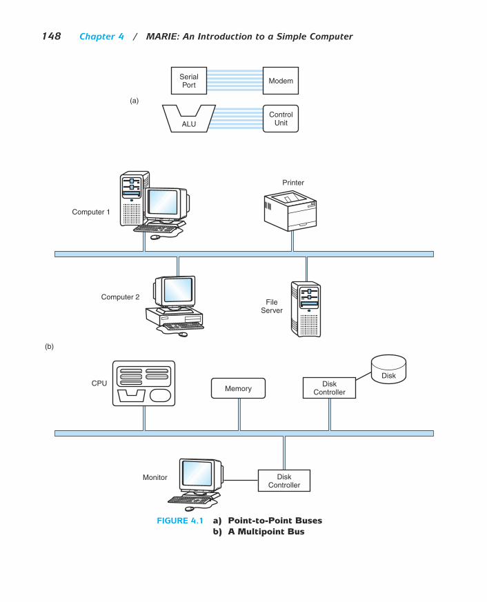
A bus can be point-to-point, connecting two specific components (as seen inFigure 4.1a) or it can be a common pathway that connects a number of devices,requiring these devices to share the bus (referred to as a multipoint bus and shownin Figure 4.1b).
148 Chapter 4 / MARIE: An Introduction to a Simple Computer
FIGURE 4.1 a) Point-to-Point Buses
b) A Multipoint Bus
SerialPort Modem
ALUControl
Unit
Computer 1
Computer 2
CPU
Monitor
FileServer
Printer
MemoryDisk
Controller
DiskController
Disk
(a)
(b)

4.1 / Introduction 149
CPU
MainMemory
Power
Address Bus
Data Bus
Control Bus
I/ODevice
I/ODevice
I/O Subsystem
FIGURE 4.2 The Components of a Typical Bus
Because of this sharing, the bus protocol (set of usage rules) is very impor-tant. Figure 4.2 shows a typical bus consisting of data lines, address lines, controllines, and power lines. Often the lines of a bus dedicated to moving data arecalled the data bus. These data lines contain the actual information that must bemoved from one location to another. Control lines indicate which device has per-mission to use the bus and for what purpose (reading or writing from memory orfrom an I/O device, for example). Control lines also transfer acknowledgmentsfor bus requests, interrupts, and clock synchronization signals. Address lines indi-cate the location (in memory, for example) that the data should be either readfrom or written to. The power lines provide the electrical power necessary. Typi-cal bus transactions include sending an address (for a read or write), transferringdata from memory to a register (a memory read), and transferring data to thememory from a register (a memory write). In addition, buses are used for I/Oreads and writes from peripheral devices. Each type of transfer occurs within abus cycle, the time between two ticks of the bus clock.
Due to the different types of information buses transport and the variousdevices that use the buses, buses themselves have been divided into differenttypes. Processor-memory buses are short, high-speed buses that are closelymatched to the memory system on the machine to maximize the bandwidth(transfer of data) and are usually very design specific. I/O buses are typicallylonger than processor-memory buses and allow for many types of devices withvarying bandwidths. These buses are compatible with many different architec-tures. A backplane bus (Figure 4.3) is actually built into the chassis of themachine and connects the processor, the I/O devices, and the memory (so alldevices share one bus). Many computers have a hierarchy of buses, so it is notuncommon to have two buses (for example a processor-memory bus and an I/Obus) or more in the same system. High-performance systems often use all threetypes of buses.

150 Chapter 4 / MARIE: An Introduction to a Simple Computer
SystemBus
InterfaceCards
FIGURE 4.3 A Backplane Bus
Personal computers have their own terminology when it comes to buses. PCshave an internal bus (called the system bus) that connects the CPU, memory, andall other internal components. External buses (sometimes referred to as expansionbuses) connect external devices, peripherals, expansion slots, and I/O ports to therest of the computer. Most PCs also have local buses, data buses that connect aperipheral device directly to the CPU. These are very high-speed buses and canbe used to connect only a limited number of similar devices. Expansion buses areslower but allow for more generic connectivity. Chapter 7 deals with these topicsin great detail.
Buses are physically little more than bunches of wires, but they have specificstandards for connectors, timing, and signaling specifications and exact protocolsfor usage. Synchronous buses are clocked, and things happen only at the clockticks (a sequence of events is controlled by the clock). Every device is synchro-nized by the rate at which the clock ticks, or the clock rate. The bus cycle timementioned earlier is the reciprocal of the bus clock rate. For example, if the busclock rate is 133MHz, then the length of the bus cycle is 1/133,000,000 or 7.52ns.Because the clock controls the transactions, any clock skew (drift in the clock) hasthe potential to cause problems, implying that the bus must be kept as short aspossible so the clock drift cannot get overly large. In addition, the bus cycle timemust not be shorter than the length of time it takes information to traverse thebus. The length of the bus, therefore, imposes restrictions on both the bus clockrate and the bus cycle time.
With asynchronous buses, control lines coordinate the operations and a complexhandshaking protocol must be used to enforce timing. To read a word of data frommemory, for example, the protocol would require steps similar to the following:
1. ReqREAD: This bus control line is activated and the data memory address is puton the appropriate bus lines at the same time.
2. ReadyDATA: This control line is asserted when the memory system has put therequired data on the data lines for the bus.
3. ACK: This control line is used to indicate that the ReqREAD or the Ready-DATA has been acknowledged.

4.1 / Introduction 151
Using a protocol instead of the clock to coordinate transactions means thatasynchronous buses scale better with technology and can support a wider varietyof devices.
To use a bus, a device must reserve it, because only one device can use the busat a time. As mentioned previously, bus masters are devices that are allowed toinitiate transfer of information (control bus) whereas bus slaves are modules thatare activated by a master and respond to requests to read and write data (so onlymasters can reserve the bus). Both follow a communications protocol to use thebus, working within very specific timing requirements. In a very simple system(such as the one we present in the next section) the processor is the only deviceallowed to become a bus master. This is good in terms of avoiding chaos, but badbecause the processor now is involved in every transaction that uses the bus.
In systems with more than one master device, bus arbitration is required. Busarbitration schemes must provide priority to certain master devices while, at thesame time, making sure lower priority devices are not starved out. Bus arbitrationschemes fall into four categories:
1. Daisy chain arbitration: This scheme uses a “grant bus” control line that ispassed down the bus from the highest priority device to the lowest priority device.(Fairness is not ensured, and it is possible that low priority devices are “starvedout” and never allowed to use the bus.) This scheme is simple but not fair.
2. Centralized parallel arbitration: Each device has a request control line to thebus, and a centralized arbiter selects who gets the bus. Bottlenecks can resultusing this type of arbitration.
3. Distributed arbitration using self-selection: This scheme is similar to centralizedarbitration but instead of a central authority selecting who gets the bus, the devicesthemselves determine who has highest priority and who should get the bus.
4. Distributed arbitration using collision detection: Each device is allowed tomake a request for the bus. If the bus detects any collisions (multiple simulta-neous requests), the device must make another request. (Ethernet uses this typeof arbitration.)
Chapter 7 contains more detailed information on buses and their protocols.
4.1.3 Clocks
Every computer contains an internal clock that regulates how quickly instructionscan be executed. The clock also synchronizes all of the components in the sys-tem. As the clock ticks, it sets the pace for everything that happens in the system,much like a metronome or a symphony conductor. The CPU uses this clock toregulate its progress, checking the otherwise unpredictable speed of the digitallogic gates. The CPU requires a fixed number of clock ticks to execute eachinstruction. Therefore, instruction performance is often measured in clockcycles—the time between clock ticks—instead of seconds. The clock frequency(sometimes called the clock rate or clock speed) is measured in MHz, as we sawin Chapter 1, where 1MHz is equal to 1 million cycles per second (so 1 hertz is 1cycle per second). The clock cycle time (or clock period) is simply the reciprocal

152 Chapter 4 / MARIE: An Introduction to a Simple Computer
of the clock frequency. For example, an 800MHz machine has a clock cycle timeof 1/800,000,000 or 1.25ns. If a machine has a 2ns cycle time, then it is a500MHz machine.
Most machines are synchronous: there is a master clock signal, which ticks(changing from 0 to 1 to 0 and so on) at regular intervals. Registers must wait forthe clock to tick before new data can be loaded. It seems reasonable to assumethat if we speed up the clock, the machine will run faster. However, there are lim-its on how short we can make the clock cycles. When the clock ticks and newdata is loaded into the registers, the register outputs are likely to change. Thesechanged output values must propagate through all the circuits in the machineuntil they reach the input of the next set of registers, where they are stored. Theclock cycle must be long enough to allow these changes to reach the next set ofregisters. If the clock cycle is too short, we could end up with some values notreaching the registers. This would result in an inconsistent state in our machine,which is definitely something we must avoid. Therefore, the minimum clockcycle time must be at least as great as the maximum propagation delay of the cir-cuit, from each set of register outputs to register inputs. What if we “shorten” thedistance between registers to shorten the propagation delay? We could do this byadding registers between the output registers and the corresponding input regis-ters. But recall that registers cannot change values until the clock ticks, so wehave, in effect, increased the number of clock cycles. For example, an instructionthat would require 2 clock cycles might now require three or four (or more,depending on where we locate the additional registers).
Most machine instructions require 1 or 2 clock cycles, but some can take 35or more. We present the following formula to relate seconds to cycles:
CPU time = = � �
It is important to note that the architecture of a machine has a large effect on itsperformance. Two machines with the same clock speed do not necessarily exe-cute instructions in the same number of cycles. For example, a multiply operationon an older Intel 286 machine required 20 clock cycles, but on a new Pentium, amultiply operation can be done in 1 clock cycle, which implies the newermachine would be 20 times faster than the 286 even if they both had the sameinternal system clock. In general, multiplication requires more time than addition,floating point operations require more cycles than integer ones, and accessingmemory takes longer than accessing registers.
Generally, when we mention the term clock, we are referring to the systemclock, or the master clock that regulates the CPU and other components. How-ever, certain buses also have their own clocks. Bus clocks are usually slower thanCPU clocks, causing bottleneck problems.
System components have defined performance bounds, indicating the maxi-mum time required for the components to perform their functions. Manufacturesguarantee their components will run within these bounds in the most extreme cir-
seconds�
cycleaverage cycles��
instructioninstructions��
programseconds�program

4.1 / Introduction 153
cumstances. When we connect all of the components together in a serial fashion,where one component must complete its task before another can function prop-erly, it is important to be aware of these performance bounds so we are able tosynchronize the components properly. However, many people push the bounds ofcertain system components in an attempt to improve system performance. Over-clocking is one method people use to achieve this goal.
Although many components are potential candidates, one of the most popularcomponents for overclocking is the CPU. The basic idea is to run the CPU atclock and/or bus speeds above the upper bound specified by the manufacturer.Although this can increase system performance, one must be careful not to createsystem timing faults, or worse yet, overheat the CPU. The system bus can also beoverclocked, which results in overclocking the various components that commu-nicate via the bus. Overclocking the system bus can provide considerable per-formance improvements, but can also damage the components that use the bus orcause them to perform unreliably.
4.1.4 The Input/Output Subsystem
Input and output (I/O) devices allow us to communicate with the computer sys-tem. I/O is the transfer of data between primary memory and various I/O periph-erals. Input devices such as keyboards, mice, card readers, scanners, voicerecognition systems, and touch screens allow us to enter data into the computer.Output devices such as monitors, printers, plotters, and speakers allow us to getinformation from the computer.
These devices are not connected directly to the CPU. Instead, there is aninterface that handles the data transfers. This interface converts the system bussignals to and from a format that is acceptable to the given device. The CPU com-municates to these external devices via input/output registers. This exchange ofdata is performed in two ways. In memory-mapped I/O, the registers in the inter-face appear in the computer’s memory map and there is no real differencebetween accessing memory and accessing an I/O device. Clearly, this is advanta-geous from the perspective of speed, but it uses up memory space in the system.With instruction-based I/O, the CPU has specialized instructions that perform theinput and output. Although this does not use memory space, it requires specificI/O instructions, which implies it can be used only by CPUs that can execute thesespecific instructions. Interrupts play a very important part in I/O, because they arean efficient way to notify the CPU that input or output is available for use.
4.1.5 Memory Organization and Addressing
We saw an example of a rather small memory in Chapter 3. However, we have notyet discussed in detail how memory is laid out and how it is addressed. It is impor-tant that you have a good understanding of these concepts before we continue.
You can envision memory as a matrix of bits. Each row, implemented by aregister, has a length typically equivalent to the word size of the machine. Each

154 Chapter 4 / MARIE: An Introduction to a Simple Computer
Address 8-bit Address 16-bit
1234...N
1234...M
(a) (b)
FIGURE 4.4 a) N 8-Bit Memory Locations
b) M 16-Bit Memory Locations
register (more commonly referred to as a memory location) has a unique address;memory addresses usually start at zero and progress upward. Figure 4.4 illustratesthis concept.
An address is almost always represented by an unsigned integer. Recall fromChapter 2 that 4 bits is a nibble, and 8 bits is a byte. Normally, memory is byte-addressable, which means that each individual byte has a unique address. Somemachines may have a word size that is larger than a single byte. For example, acomputer might handle 32-bit words (which means it can manipulate 32 bits at atime through various instructions), but still employ a byte-addressable architec-ture. In this situation, when a word uses multiple bytes, the byte with the lowestaddress determines the address of the entire word. It is also possible that a com-puter might be word-addressable, which means each word (not necessarily eachbyte) has its own address, but most current machines are byte-addressable (eventhough they have 32-bit or larger words). A memory address is typically stored ina single machine word.
If all this talk about machines using byte-addressing with words of differentsizes has you somewhat confused, the following analogy may help. Memory issimilar to a street full of apartment buildings. Each building (word) has multipleapartments (bytes), and each apartment has its own address. All of the apartmentsare numbered sequentially (addressed), from 0 to the total number of apartmentsin the complex. The buildings themselves serve to group the apartments. In com-puters, words do the same thing. Words are the basic unit of size used in variousinstructions. For example, you may read a word from or write a word to memory,even on a byte-addressable machine.
If an architecture is byte-addressable, and the instruction set architecture word islarger than 1 byte, the issue of alignment must be addressed. For example, if we wishto read a 32-bit word on a byte-addressable machine, we must make sure that: (1) theword was stored on a natural alignment boundary, and (2) the access starts on thatboundary. This is accomplished, in the case of 32-bit words, by requiring the addressto be a multiple of 4. Some architectures allow unaligned accesses, where the desiredaddress does not have to start on a natural boundary.
Memory is built from random access memory (RAM) chips. (We cover mem-ory in detail in Chapter 6.) Memory is often referred to using the notation L � W(length � width). For example, 4M � 16 means the memory is 4M long (it has

4.1 / Introduction 155
Total ItemsTotal as a Power of 2Number of Bits
221
1
422
2
823
3
1624
4
3225
??
TABLE 4.1 Calculating the Address Bits Required
Row 0
Row 1
Row 15
2K � 8 2K � 8
2K � 8 2K � 8
2K � 8 2K � 8
•••
FIGURE 4.5 Memory as a Collection of RAM Chips
4M = 22 � 220 = 222 words) and it is 16 bits wide (each word is 16 bits). Thewidth (second number of the pair) represents the word size. To address this mem-ory (assuming word addressing), we need to be able to uniquely identify 212 dif-ferent items, which means we need 212 different addresses. Since addresses areunsigned binary numbers, we need to count from 0 to (212 � 1) in binary. Howmany bits does this require? Well, to count from 0 to 3 in binary (for a total of 4items), we need 2 bits. To count from 0 to 7 in binary (for a total of 8 items), weneed 3 bits. To count from 0 to 15 in binary (for a total of 16 items), we need 4bits. Do you see a pattern emerging here? Can you fill in the missing value forTable 4.1?
The correct answer is 5 bits. In general, if a computer has 2N addressableunits of memory, it will require N bits to uniquely address each byte.
Main memory is usually larger than one RAM chip. Consequently, thesechips are combined into a single memory module to give the desired memorysize. For example, suppose you need to build a 32K � 16 memory and all youhave are 2K � 8 RAM chips. You could connect 16 rows and 2 columns of chipstogether as shown in Figure 4.5.
Each row of chips addresses 2K words (assuming the machine is word-addressable), but it requires two chips to handle the full width. Addresses for thismemory must have 15 bits (there are 32K = 25 � 210 words to access). But eachchip pair (each row) requires only 11 address lines (each chip pair holds only 211
words). In this situation, a decoder would be needed to decode the leftmost 4 bitsof the address to determine which chip pair holds the desired address. Once theproper chip pair has been located, the remaining 11 bits would be input intoanother decoder to find the exact address within the chip pair.
A single shared memory module causes sequentialization of access. Memoryinterleaving, which splits memory across multiple memory modules (or banks),

156 Chapter 4 / MARIE: An Introduction to a Simple Computer
Module 1
0
1
2
3
Module 2
4
5
6
7
Module 3
8
9
10
11
Module 4
12
13
14
15
Module 5
16
17
18
19
Module 6
20
21
22
23
Module 7
24
25
26
27
Module 8
28
29
30
31
FIGURE 4.6 High-Order Memory Interleaving
Module 1
0
8
16
24
Module 2
1
9
17
25
Module 3
2
10
18
26
Module 4
3
11
19
27
Module 5
4
12
20
28
Module 6
5
13
21
29
Module 7
6
14
22
30
Module 8
7
15
23
31
FIGURE 4.7 Low-Order Memory Interleaving
can be used to help relieve this. With low-order interleaving, the low-order bits ofthe address are used to select the bank; in high-order interleaving, the high-orderbits of the address are used.
High-order interleaving, the more intuitive organization, distributes theaddresses so that each module contains consecutive addresses, as we see with the32 addresses in Figure 4.6.
Low-order interleaved memory places consecutive words of memory in dif-ferent memory modules. Figure 4.7 shows low-order interleaving on 32addresses.
With the appropriate buses using low-order interleaving, a read or write usingone module can be started before a read or write using another module actuallycompletes (reads and writes can be overlapped).
The memory concepts we have covered are very important and appear in var-ious places in the remaining chapters, in particular in Chapter 6, which discussesmemory in detail. The key concepts to focus on are: (1) Memory addresses areunsigned binary values (although we often view them as hex values because it iseasier), and (2) The number of items to be addressed determines the numbers ofbits that occur in the address. Although we could always use more bits for theaddress than required, that is seldom done because minimization is an importantconcept in computer design.
4.1.6 Interrupts
We have introduced the basic hardware information required for a solid under-standing of computer architecture: the CPU, buses, the control unit, registers,clocks, I/O, and memory. However, there is one more concept we need to coverthat deals with how these components interact with the processor: Interrupts are

4.2 / MARIE 157
events that alter (or interrupt) the normal flow of execution in the system. Aninterrupt can be triggered for a variety of reasons, including:
• I/O requests• Arithmetic errors (e.g., division by zero)• Arithmetic underflow or overflow• Hardware malfunction (e.g., memory parity error)• User-defined break points (such as when debugging a program)• Page faults (this is covered in detail in Chapter 6)• Invalid instructions (usually resulting from pointer issues)• Miscellaneous
The actions performed for each of these types of interrupts (called interrupthandling) are very different. Telling the CPU that an I/O request has finished ismuch different from terminating a program because of division by zero. But theseactions are both handled by interrupts because they require a change in the nor-mal flow of the program’s execution.
An interrupt can be initiated by the user or the system, can be maskable (dis-abled or ignored) or nonmaskable (a high priority interrupt that cannot be dis-abled and must be acknowledged), can occur within or between instructions, maybe synchronous (occurs at the same place every time a program is executed) orasynchronous (occurs unexpectedly), and can result in the program terminating orcontinuing execution once the interrupt is handled. Interrupts are covered in moredetail in Section 4.3.2 and in Chapter 7.
Now that we have given a general overview of the components necessary fora computer system to function, we proceed by introducing a simple, yet func-tional, architecture to illustrate these concepts.
4.2 MARIE
MARIE, a Machine Architecture that is Really Intuitive and Easy, is a simplearchitecture consisting of memory (to store programs and data) and a CPU (con-sisting of an ALU and several registers). It has all the functional components nec-essary to be a real working computer. MARIE will help illustrate the concepts inthis and the preceding three chapters. We describe MARIE’s architecture in thefollowing sections.
4.2.1 The Architecture
MARIE has the following characteristics:
• Binary, two’s complement• Stored program, fixed word length• Word (but not byte) addressable• 4K words of main memory (this implies 12 bits per address)

158 Chapter 4 / MARIE: An Introduction to a Simple Computer
• 16-bit data (words have 16 bits)• 16-bit instructions, 4 for the opcode and 12 for the address• A 16-bit accumulator (AC)• A 16-bit instruction register (IR)• A 16-bit memory buffer register (MBR)• A 12-bit program counter (PC)• A 12-bit memory address register (MAR)• An 8-bit input register• An 8-bit output register
Figure 4.8 shows the architecture for MARIE.Before we continue, we need to stress one important point about memory. In
Chapter 8, we presented a simple memory built using D flip-flops. We emphasizeagain that each location in memory has a unique address (represented in binary)and each location can hold a value. These notions of the address versus what isactually stored at that address tend to be confusing. To help avoid confusion, justvisualize a post office. There are post office boxes with various “addresses” ornumbers. Inside the post office box, there is mail. To get the mail, the number ofthe post office box must be known. The same is true for data or instructions thatneed to be fetched from memory. The contents of any memory address are manip-ulated by specifying the address of that memory location. We shall see that thereare many different ways to specify this address.
Memory Address 0
Memory Address 4K–1
ALUAC
OutREG
InREG
MBR MAR
PC IR
Control Unit
The CPU
MainMemory
FIGURE 4.8 MARIE’s Architecture

4.2 / MARIE 159
4.2.2 Registers and Buses
Registers are storage locations within the CPU (as illustrated in Figure 4.8). TheALU (arithmetic logic unit) portion of the CPU performs all of the processing(arithmetic operations, logic decisions, and so on). The registers are used for veryspecific purposes when programs are executing: They hold values for temporarystorage, data that is being manipulated in some way, or results of simple calcula-tions. Many times, registers are referenced implicitly in an instruction, as we seewhen we describe the instruction set for MARIE that follows in Section 4.2.3.
In MARIE, there are seven registers, as follows:
• AC: The accumulator, which holds data values. This is a general purpose reg-ister and holds data that the CPU needs to process. Most computers today havemultiple general purpose registers.
• MAR: The memory address register, which holds the memory address of thedata being referenced.
• MBR: The memory buffer register, which holds either the data just read frommemory or the data ready to be written to memory.
• PC: The program counter, which holds the address of the next instruction tobe executed in the program.
• IR: The instruction register, which holds the next instruction to be executed.• InREG: The input register, which holds data from the input device.• OutREG: The output register, which holds data for the output device.
The MAR, MBR, PC, and IR hold very specific information and cannot beused for anything other than their stated purposes. For example, we could notstore an arbitrary data value from memory in the PC. We must use the MBR or theAC to store this arbitrary value. In addition, there is a status or flag register thatholds information indicating various conditions, such as an overflow in the ALU.However, for clarity, we do not include that register explicitly in any figures.
MARIE is a very simple computer with a limited register set. Modern CPUshave multiple general purpose registers, often called user-visible registers, thatperform functions similar to those of the AC. Today’s computers also have addi-tional registers; for example, some computers have registers that shift data valuesand other registers that, if taken as a set, can be treated as a list of values.
MARIE cannot transfer data or instructions into or out of registers without abus. In MARIE, we assume a common bus scheme. Each device connected to thebus has a number, and before the device can use the bus, it must be set to thatidentifying number. We also have some pathways to speed up execution. We havea communication path between the MAR and memory (the MAR provides theinputs to the address lines for memory so the CPU knows where in memory toread or write), and a separate path from the MBR to the AC. There is also a spe-cial path from the MBR to the ALU to allow the data in the MBR to be used inarithmetic operations. Information can also flow from the AC through the ALUand back into the AC without being put on the common bus. The advantagegained using these additional pathways is that information can be put on the com-

160 Chapter 4 / MARIE: An Introduction to a Simple Computer
Bus
16-bit bus
0
1
2
3
4
5
6
7
Main Memory
MAR
PC
MBR
AC
InREG
OutREG
IR
ALU
FIGURE 4.9 The Data Path in MARIE
mon bus in the same clock cycle in which data is put on these other pathways,allowing these events to take place in parallel. Figure 4.9 shows the data path (thepath that information follows) in MARIE.
4.2.3 The Instruction Set Architecture
MARIE has a very simple, yet powerful, instruction set. The instruction set archi-tecture (ISA) of a machine specifies the instructions that the computer can per-form and the format for each instruction. The ISA is essentially an interfacebetween the software and the hardware. Some ISAs include hundreds of instruc-tions. We mentioned previously that each instruction for MARIE consists of 16bits. The most significant 4 bits, bits 12–15, make up the opcode that specifies theinstruction to be executed (which allows for a total of 16 instructions). The leastsignificant 12 bits, bits 0–11, form an address, which allows for a maximummemory size of 212–1. The instruction format for MARIE is shown in Figure 4.10.

4.2 / MARIE 161
Opcode Address
15Bit 12 11 0
FIGURE 4.10 MARIE’s Instruction Format
TABLE 4.2 MARIE’s Instruction Set
Most ISAs consist of instructions for processing data, moving data, and con-trolling the execution sequence of the program. MARIE’s instruction set consistsof the instructions shown in Table 4.2.
The Load instruction allows us to move data from memory into the CPU (viathe MBR and the AC). All data (which includes anything that is not an instruction)from memory must move first into the MBR and then into either the AC or theALU; there are no other options in this architecture. Notice that the Load instruc-tion does not have to name the AC as the final destination; this register is implicitin the instruction. Other instructions reference the AC register in a similar fashion.The Store instruction allows us to move data from the CPU back to memory. TheAdd and Subt instructions add and subtract, respectively, the data value found ataddress X to or from the value in the AC. The data located at address X is copiedinto the MBR where it is held until the arithmetic operation is executed. Input andOutput allow MARIE to communicate with the outside world.
Input and output are complicated operations. In modern computers, input andoutput are done using ASCII bytes. This means that if you type in the number 32on the keyboard as input, it is actually read in as the ASCII character “3” fol-lowed by “2.” These two characters must be converted to the numeric value 32before they are stored in the AC. Because we are focusing on how a computerworks, we are going to assume that a value input from the keyboard is “automati-cally” converted correctly. We are glossing over a very important concept: Howdoes the computer know whether an input/output value is to be treated as numericor ASCII, if everything that is input or output is actually ASCII? The answer is
Instruction Number
Hex
1234
56789
Load the contents of address X into AC.Store the contents of AC at address X.Add the contents of address X to AC and store the result in AC.Subtract the contents of address X from AC and store theresult in AC.Input a value from the keyboard into AC.Output the value in AC to the display.Terminate the program.Skip the next instruction on condition.Load the value of X into PC.
Instruction
Load XStore XAdd XSubt X
InputOutputHaltSkipcondJump X
Meaning
0001001000110100
01010110011110001001
Bin

162 Chapter 4 / MARIE: An Introduction to a Simple Computer
that the computer knows through the context of how the value is used. InMARIE, we assume numeric input and output only. We also allow values to beinput as decimal and assume there is a “magic conversion” to the actual binaryvalues that are stored. In reality, these are issues that must be addressed if a com-puter is to work properly.
The Halt command causes the current program execution to terminate. TheSkipcond instruction allows us to perform conditional branching (as is done with“while” loops or “if” statements). When the Skipcond instruction is executed, thevalue stored in the AC must be inspected. Two of the address bits (let’s assumewe always use the two address bits closest to the opcode field, bits 10 and 11)specify the condition to be tested. If the two address bits are 00, this translates to“skip if the AC is negative.” If the two address bits are 01 (bit eleven is 0 and bitten is 1), this translates to “skip if the AC is equal to 0.” Finally, if the twoaddress bits are 10 (or 2), this translates to “skip if the AC is greater than 0.” By“skip” we simply mean jump over the next instruction. This is accomplished byincrementing the PC by 1, essentially ignoring the following instruction, which isnever fetched. The Jump instruction, an unconditional branch, also affects the PC.This instruction causes the contents of the PC to be replaced with the value of X,which is the address of the next instruction to fetch.
We wish to keep the architecture and the instruction set as simple as possibleand yet convey the information necessary to understand how a computer works.Therefore, we have omitted several useful instructions. However, you will seeshortly that this instruction set is still quite powerful. Once you gain familiaritywith how the machine works, we will extend the instruction set to make program-ming easier.
Let’s examine the instruction format used in MARIE. Suppose we have thefollowing 16-bit instruction:
The leftmost 4 bits indicate the opcode, or the instruction to be executed.0001 is binary for 1, which represents the Load instruction. The remaining 12 bitsindicate the address of the value we are loading, which is address 3 in main mem-ory. This instruction causes the data value found in main memory, address 3, to becopied into the AC. Consider another instruction:
The leftmost four bits, 0011, are equal to 3, which is the Add instruction. Theaddress bits indicate address 00D in hex (or 13 decimal). We go to main memory,get the data value at address 00D, and add this value to the AC. The value in theAC would then change to reflect this sum. One more example follows:
0 0 1 1 0 0 0 0 0 0 0 0 1 1 0 1
Bit 151413121110 9 8 7 6 5 4 3 2 1 0
addressopcode
0 0 0 1 0 0 0 0 0 0 0 0 0 0 1 1
Bit 151413121110 9 8 7 6 5 4 3 2 1 0
addressopcode

4.2 / MARIE 163
The opcode for this instruction represents the Skipcond instruction. Bits tenand eleven (read left to right, or bit eleven followed by bit ten) are 10, indicatinga value of 2. This implies a “skip if AC greater than or equal to 0.” If the value inthe AC is less than zero, this instruction is ignored and we simply go on to thenext instruction. If the value in the AC is greater than or equal to zero, thisinstruction causes the PC to be incremented by 1, thus causing the instructionimmediately following this instruction in the program to be ignored (keep this inmind as you read the following section on the instruction cycle).
These examples bring up an interesting point. We will be writing programsusing this limited instruction set. Would you rather write a program using thecommands Load, Add, and Halt, or their binary equivalents 0001, 0011, and0111? Most people would rather use the instruction name, or mnemonic, for theinstruction, instead of the binary value for the instruction. Our binary instructionsare called machine instructions. The corresponding mnemonic instructions arewhat we refer to as assembly language instructions. There is a one-to-one corre-spondence between assembly language and machine instructions. When we typein an assembly language program (i.e., using the instructions listed in Table 4.2),we need an assembler to convert it to its binary equivalent. We discuss assem-blers in Section 4.5.
4.2.4 Register Transfer Notation
We have seen that digital systems consist of many components, including arith-metic logic units, registers, memory, decoders, and control units. These units areinterconnected by buses to allow information to flow through the system. Theinstruction set presented for MARIE in the preceding sections constitutes a set ofmachine level instructions used by these components to execute a program. Eachinstruction appears to be very simplistic; however, if you examine what actuallyhappens at the component level, each instruction involves multiple operations.For example, the Load instruction loads the contents of the given memory loca-tion into the AC register. But, if we observe what is happening at the componentlevel, we see that multiple “mini-instructions” are being executed. First, theaddress from the instruction must be loaded into the MAR. Then the data inmemory at this location must be loaded into the MBR. Then the MBR must beloaded into the AC. These mini-instructions are called microoperations and spec-ify the elementary operations that can be performed on data stored in registers.
The symbolic notation used to describe the behavior of microoperations iscalled register transfer notation (RTN) or register transfer language (RTL). Weuse the notation M[X] to indicate the actual data stored at location X in memory,and ← to indicate a transfer of information. In reality, a transfer from one registerto another always involves a transfer onto the bus from the source register, andthen a transfer off the bus into the destination register. However, for the sake of
1 0 0 0 1 0 0 0 0 0 0 0 0 0 0 0
Bit 151413121110 9 8 7 6 5 4 3 2 1 0
addressopcode

164 Chapter 4 / MARIE: An Introduction to a Simple Computer
clarity, we do not include these bus transfers, assuming that you understand thatthe bus must be used for data transfer.
We now present the register transfer notation for each of the instructions inthe ISA for MARIE.
Load X
Recall that this instruction loads the contents of memory location X into the AC.However, the address X must first be placed into the MAR. Then the data at loca-tion M[MAR] (or address X) is moved into the MBR. Finally, this data is placedin the AC.
MAR ← X
MBR ← M[MAR], AC ← MBR
Because the IR must use the bus to copy the value of X into the MAR, beforethe data at location X can be placed into the MBR, this operation requires two buscycles. Therefore, these two operations are on separate lines to indicate they cannotoccur during the same cycle. However, because we have a special connectionbetween the MBR and the AC, the transfer of the data from the MBR to the AC canoccur immediately after the data is put into the MBR, without waiting for the bus.
Store X
This instruction stores the contents of the AC in memory location X:
MAR ← X, MBR ← AC
M[MAR] ← MBR
Add X
The data value stored at address X is added to the AC. This can be accomplishedas follows:
MAR ← X
MBR ← M[MAR]
AC ← AC + MBR
Subt X
Similar to Add, this instruction subtracts the value stored at address X from theaccumulator and places the result back in the AC:
MAR ← X
MBR ← M[MAR]
AC ← AC � MBR

4.2 / MARIE 165
Input
Any input from the input device is first routed into the InREG. Then the data istransferred into the AC.
AC ← InREG
Output
This instruction causes the contents of the AC to be placed into the OutREG,where it is eventually sent to the output device.
OutREG ← AC
Halt
No operations are performed on registers; the machine simply ceases execution.
Skipcond
Recall that this instruction uses the bits in positions 10 and 11 in the address fieldto determine what comparison to perform on the AC. Depending on this bit com-bination, the AC is checked to see whether it is negative, equal to zero, or greaterthan zero. If the given condition is true, then the next instruction is skipped. Thisis performed by incrementing the PC register by 1.
if IR[11–10] = 00 then {if bits 10 and 11 in the IR are both 0}
If AC < 0 then PC ← PC+1
else If IR[11–10] = 01 then {if bit 11 = 0 and bit 10 = 1}
If AC = 0 then PC ← PC + 1
else If IR[11–10] = 10 then {if bit 11 = 1 and bit 10 = 0}
If AC > 0 then PC ← PC + 1
If the bits in positions ten and eleven are both ones, an error condition results.However, an additional condition could also be defined using these bit values.
Jump X
This instruction causes an unconditional branch to the given address, X. There-fore, to execute this instruction, X must be loaded into the PC.
PC ← X
In reality, the lower or least significant 12 bits of the instruction register(or IR[11–0]) reflect the value of X. So this transfer is more accuratelydepicted as:
PC ← IR[11–0]
However, we feel that the notation PC ← X is easier to understand and relateto the actual instructions, so we use this instead.
Register transfer notation is a symbolic means of expressing what is happen-ing in the system when a given instruction is executing. RTN is sensitive to the

166 Chapter 4 / MARIE: An Introduction to a Simple Computer
data path, in that if multiple microoperations must share the bus, they must beexecuted in a sequential fashion, one following the other.
4.3 INSTRUCTION PROCESSING
Now that we have a basic language with which to communicate ideas to our com-puter, we need to discuss exactly how a specific program is executed. All comput-ers follow a basic machine cycle: the fetch, decode, and execute cycle.
4.3.1 The Fetch-Decode-Execute Cycle
The fetch-decode-execute cycle represents the steps that a computer follows to runa program. The CPU fetches an instruction (transfers it from main memory to theinstruction register), decodes it (determines the opcode and fetches any data neces-sary to carry out the instruction), and executes it (performs the operation(s) indi-cated by the instruction). Notice that a large part of this cycle is spent copying datafrom one location to another. When a program is initially loaded, the address of thefirst instruction must be placed in the PC. The steps in this cycle, which take placein specific clock cycles, are listed below. Note that Steps 1 and 2 make up the fetchphase, Step 3 makes up the decode phase, and Step 4 is the execute phase.
1. Copy the contents of the PC to the MAR: MAR ← PC.
2. Go to main memory and fetch the instruction found at the address in the MAR,placing this instruction in the IR; increment PC by 1 (PC now points to thenext instruction in the program): IR ← M[MAR] and then PC ← PC+1. (Note:Because MARIE is word-addressable, the PC is incremented by one, whichresults in the next word’s address occupying the PC. If MARIE were byte-addressable, the PC would need to be incremented by 2 to point to the addressof the next instruction, because each instruction would require two bytes. On abyte-addressable machine with 32-bit words, the PC would need to be incre-mented by 4.)
3. Copy the rightmost 12 bits of the IR into the MAR; decode the leftmost fourbits to determine the opcode, MAR ← IR[11–0], and decode IR[15–12].
4. If necessary, use the address in the MAR to go to memory to get data, placingthe data in the MBR (and possibly the AC), and then execute the instructionMBR ← M[MAR] and execute the actual instruction.
This cycle is illustrated in the flowchart in Figure 4.11.Note that computers today, even with large instruction sets, long instructions,
and huge memories, can execute millions of these fetch-decode-execute cycles inthe blink of an eye.
4.3.2 Interrupts and I/O
Chapter 7 is dedicated to input and output. However, we will discuss some basicconcepts of I/O at this point, to make sure you understand the entire process ofhow a program executes.

4.3 / Instruction Processing 167
Start
Copy the PC tothe MAR
Copy the contents ofmemory at address
MAR to IR;Increment PC by 1
Decode the instruction andplace bits IR[11-0] in
MAR
Instructionrequires
operand?
Yes No
Copy the contents ofmemory at address
MAR to MBR
Execute theinstruction
FIGURE 4.11 The Fetch-Decode-Execute Cycle
MARIE has two registers to accommodate input and output. The input regis-ter holds data being transferred from an input device into the computer; the out-put register holds information ready to be sent to an output device. The timingused by these two registers is very important. For example, if you are enteringinput from the keyboard and type very fast, the computer must be able to readeach character that is put into the input register. If another character is enteredinto that register before the computer has a chance to process the current charac-ter, the current character is lost. It is more likely, since the processor is very fastand keyboard input is very slow, that the processor might read the same characterfrom the input register multiple times. We must avoid both of these situations.
MARIE addresses these problems by using interrupt-driven I/O. (A detaileddiscussion of the various types of I/O can be found in Chapter 7.) When the CPUexecutes an input or output instruction, the appropriate I/O device is notified. The

168 Chapter 4 / MARIE: An Introduction to a Simple Computer
Has aninterrupt been
issued?
Yes No
Process theinterrupt
Perform fetch-decode-execute
cycle
FIGURE 4.12 Modified Instruction Cycle to Check for Interrupt
CPU then continues with other useful work until the device is ready. At that time,the device sends an interrupt signal to the CPU. The CPU then processes theinterrupt, after which it continues with the normal fetch-decode-execute cycle.This process requires the following:
• A signal (interrupt) from the I/O device to the CPU indicating that input or out-put is complete
• Some means of allowing the CPU to detour from the usual fetch-decode-exe-cute cycle to “recognize” this interrupt
The method most computers use to process an interrupt is to check to see ifan interrupt is pending at the beginning of each fetch-decode-execute cycle. If so,the interrupt is processed, after which the machine execution cycle continues. Ifno interrupt is present, processing continues as normal. The path of execution isillustrated in the flowchart in Figure 4.12.
Typically, the input or output device sends an interrupt by using a special reg-ister, the status or flag register. A special bit is set to indicate an interrupt hasoccurred. For example, as soon as input is entered from the keyboard, this bit isset. The CPU checks this bit at the beginning of every machine cycle. When it isset, the CPU processes an interrupt. When it is not set, the CPU performs a normalfetch-decode-execute cycle, processing instructions in the program it is currentlyexecuting.
When the CPU finds the interrupt bit set it executes an interrupt routine thatis determined by the type of interrupt that has occurred. Input/output interruptsare not the only types of interrupts that can occur when a program is executing.Have you ever typed a Ctrl-break or Ctrl-C to stop a program? This is anotherexample of an interrupt. There are external interrupts generated by an externalevent (such as input/output or power failure), internal interrupts generated bysome exception condition in the program (such as division by zero, stack over-flow, or protection violations) and software interrupts generated by executing an

4.4 / A Simple Program 169
instruction in the program (such as one that requires a program to switch fromrunning at one level, such as user level, to another level, such as kernel level).
Regardless of which type of interrupt has been invoked, the interrupt handlingprocess is the same. After the CPU recognizes an interrupt request, the address ofthe interrupt service routine is determined (usually by hardware) and the routine(very much like a procedure) is executed. The CPU switches from running the pro-gram to running a specialized procedure to deal with the interrupt. The normalfetch-decode-execute cycle is run on the instructions in the interrupt service routineuntil that code has been run to completion. The CPU then switches back to the pro-gram it was running before the interrupt occurred. The CPU must return to the exactpoint at which it was running in the original program. Therefore, when the CPUswitches to the interrupt service routine, it must save the contents of the PC, thecontents of all other registers in the CPU, and any status conditions that exist for theoriginal program. When the interrupt service routine is finished, the CPU restoresthe exact same environment in which the original program was running, and thenbegins fetching, decoding, and executing instructions for the original program.
4.4 A SIMPLE PROGRAM
We now present a simple program written for MARIE. In Section 4.6, we presentseveral additional examples to illustrate the power of this minimal architecture. Itcan even be used to run programs with procedures, various looping constructs,and different selection options.
Our first program adds two numbers together (both of which are found inmain memory), storing the sum in memory. (We forgo input/output for now.)
Table 4.3 lists an assembly language program to do this, along with its corre-sponding machine-language program. The list of instructions under the Instruc-tion column constitutes the actual assembly language program. We know that thefetch-decode-execute cycle starts by fetching the first instruction of the program,which it finds by loading the PC with the address of the first instruction when theprogram is loaded for execution. For simplicity, let’s assume our programs inMARIE are always loaded starting at address 100 (in hex).
The list of instructions under the Binary Contents of Memory Address col-umn constitutes the actual machine language program. It is often easier for
HexAddress Instruction Binary Contents of
Memory AddressHex Contents
of Memory
100101102103104105106
Load 104Add 105Store 106Halt0023FFE90000
0001000100000100001100010000010100100001000001100111000000000000000000000010001111111111111010010000000000000000
11043105210670000023FFE90000
TABLE 4.3 A Program to Add Two Numbers

170 Chapter 4 / MARIE: An Introduction to a Simple Computer
humans to read hexadecimal as opposed to binary, so the actual contents of mem-ory are displayed in hexadecimal.
This program loads 002316 (or decimal value 35) into the AC. It then adds thehex value FFE9 (decimal �23) that it finds at address 105. This results in a valueof 12 in the AC. The Store instruction stores this value at memory location 106.When the program is done, the binary contents of location 106 change to0000000000001100, which is hex 000C, or decimal 12. Figure 4.13 indicates thecontents of the registers as the program executes.
The last RTN instruction in Part c places the sum at the proper memory loca-tion. The statement “decode IR[15–12]” simply means the instruction must bedecoded to determine what is to be done. This decoding can be done in software(using a microprogram) or in hardware (using hardwired circuits). These two con-cepts are covered in more detail in Section 4.7.
Note that there is a one-to-one correspondence between the assembly lan-guage and the machine language instructions. This makes it easy to convertassembly language into machine code. Using the instruction tables given in thischapter, you should be able to hand assemble any of our example programs. Forthis reason, we look at only the assembly language code from this point on.Before we present more programming examples, however, a discussion of theassembly process is in order.
4.5 A DISCUSSION ON ASSEMBLERS
In the program shown in Table 4.3 it is a simple matter to convert from theassembly language instruction Load 104, for example, to the machine lan-guage instruction 1104 (in hex). But why bother with this conversion? Whynot just write in machine code? Although it is very efficient for computers tosee these instructions as binary numbers, it is difficult for human beings tounderstand and program in sequences of zeros and ones. We prefer words andsymbols over long numbers, so it seems a natural solution to devise a pro-gram that does this simple conversion for us. This program is called anassembler.
4.5.1 What Do Assemblers Do?
An assembler’s job is to convert assembly language (using mnemonics) intomachine language (which consists entirely of binary values, or strings of zerosand ones). Assemblers take a programmer’s assembly language program,which is really a symbolic representation of the binary numbers, and convertit into binary instructions, or the machine code equivalent. The assemblerreads a source file (assembly program) and produces an object file (themachine code).
Substituting simple alphanumeric names for the opcodes makes programmingmuch easier. We can also substitute labels (simple names) to identify or name par-ticular memory addresses, making the task of writing assembly programs evensimpler. For example, in our program to add two numbers, we can use labels to

4.5 / A Discussion on Assemblers 171
FIGURE 4.13 A Trace of the Program to Add Two Numbers
Step RTN PC IR MAR MBR AC
(initial values)Fetch
Decode
Get operandExecute
MAR PCIR M[MAR]PC PC + 1MAR IR[11—0](Decode IR[15—12])MBR M[MAR]AC MBR
100100100101101101101101
------------110411041104110411041104
------100100100104104104104
------------------------------------00230023
------------------------------------------0023
a) Load 104
Step RTN PC IR MAR MBR AC
(initial values)Fetch
Decode
Get operandExecute
MAR PCIR M[MAR]PC PC + 1MAR IR[11—0](Decode IR[15—12])MBR M[MAR]AC AC + MBR
101101101102102102102102
11041104310531053105310531053105
104101101101105105105105
002300230023002300230023FFE9FFE9
0023002300230023002300230023000C
b) Add 105
Step RTN PC IR MAR MBR AC
(initial values)Fetch
Decode
Get operandExecute
MAR PCIR M[MAR]PC PC + 1MAR IR[11—0](Decode IR[15—12])(not necessary)MBR ACM[MAR] MBR
102102102103103103103103103
310531052106210621062106210621062106
105102102102106106106106106
FFE9FFE9FFE9FFE9FFE9FFE9FFE9000C000C
000C000C000C000C000C000C000C000C000C
c) Store 106

172 Chapter 4 / MARIE: An Introduction to a Simple Computer
Address Instruction
100101102103104105106
Load XAdd YStore ZHalt0023FFE90000
X,Y,Z,
TABLE 4.4 An Example Using Labels
indicate the memory addresses, thus making it unnecessary to know the exactmemory address of the operands for instructions. Table 4.4 illustrates this concept.
When the address field of an instruction is a label instead of an actual physicaladdress, the assembler still must translate it into a real, physical address in mainmemory. Most assembly languages allow for labels. Assemblers typically specifyformatting rules for their instructions, including those with labels. For example, alabel might be limited to three characters and may also be required to occur as thefirst field in the instruction. MARIE requires labels to be followed by a comma.
Labels are nice for programmers. However, they make more work for theassembler. It must make two passes through a program to do the translation. Thismeans the assembler reads the program twice, from top to bottom each time. On thefirst pass, the assembler builds a set of correspondences called a symbol table. Forthe above example, it builds a table with three symbols: X, Y, and Z. Because anassembler goes through the code from top to bottom, it cannot translate the entireassembly language instruction into machine code in one pass; it does not knowwhere the data portion of the instruction is located if it is given only a label. Butafter it has built the symbol table, it can make a second pass and “fill in the blanks.”
In the above program, the first pass of the assembler creates the followingsymbol table:
It also begins to translate the instructions. After the first pass, the translatedinstructions would be incomplete as follows:
On the second pass, the assembler uses the symbol table to fill in the addressesand create the corresponding machine language instructions. Thus, on the second
1
3
2
7
X
Y
Z
00 0
X
Y
Z
104
105
106

4.5 / A Discussion on Assemblers 173
pass it would know that X is located at address 104, and would then substitute 104for the X. A similar procedure would replace the Y and Z, resulting in:
Because most people are uncomfortable reading hexadecimal, most assemblylanguages allow the data values stored in memory to be specified as binary, hexa-decimal, or decimal. Typically, some sort of assembler directive (an instructionspecifically for the assembler that is not supposed to be translated into machinecode) is given to the assembler to specify which base is to be used to interpret thevalue. We use DEC for decimal and HEX for hexadecimal in MARIE’s assemblylanguage. For example, we rewrite the program in Table 4.4 as shown in Table 4.5.
Instead of requiring the actual binary data value (written in hex), we specify adecimal value by using the directive DEC. The assembler recognizes this direc-tive and converts the value accordingly before storing it in memory. Again, direc-tives are not converted to machine language; they simply instruct the assemblerin some way.
Another kind of directive common to virtually every programming languageis the comment delimiter. Comment delimiters are special characters that tell theassembler (or compiler) to ignore all text following the special character.MARIE’s comment delimiter is a front slash (“/”), which causes all text betweenthe delimiter and the end of the line to be ignored.
4.5.2 Why Use Assembly Language?
Our main objective in presenting MARIE’s assembly language is to give you anidea of how the language relates to the architecture. Understanding how to pro-gram in assembly goes a long way toward understanding the architecture (andvice versa). Not only do you learn basic computer architecture, but you also canlearn exactly how the processor works and gain significant insight into the partic-ular architecture on which you are programming. There are many other situationswhere assembly programming is useful.
1
3
2
7
1
1
1
0
0
0
0
0
4
5
6
0
Address Instruction
100101102103104105106
Load XAdd YStore ZHaltDEC 35DEC –23HEX 0000
X,Y,Z,
TABLE 4.5 An Example Using Directives for Constants

174 Chapter 4 / MARIE: An Introduction to a Simple Computer
Most programmers agree that 10% of the code in a program uses approxi-mately 90% of the CPU time. In time-critical applications, we often need to opti-mize this 10% of the code. Typically, the compiler handles this optimization for us.The compiler takes a high-level language (such as C++) and converts it into assem-bly language (which is then converted into machine code). Compilers have beenaround a long time and in most cases they do a great job. Occasionally, however,programmers must bypass some of the restrictions found in high-level languagesand manipulate the assembly code themselves. By doing this, programmers canmake the program more efficient in terms of time (and space). This hybridapproach (most of the program written in a high-level language, with part rewrittenin assembly) allows the programmer to take advantage of the best of both worlds.
Are there situations in which entire programs should be written in assemblylanguage? If the overall size of the program or response time is critical, assemblylanguage often becomes the language of choice. This is because compilers tend toobscure information about the cost (in time) of various operations and programmersoften find it difficult to judge exactly how their compiled programs will perform.Assembly language puts the programmer closer to the architecture, and thus, infirmer control. Assembly language might actually be necessary if the programmerwishes to accomplish certain operations not available in a high-level language.
A perfect example, in terms of both response performance and space-criticaldesign, is found in embedded systems. These are systems in which the computeris integrated into a device that is typically not a computer. Embedded systemsmust be reactive and often are found in time-constrained environments. Thesesystems are designed to perform either a single instruction or a very specific setof instructions. Chances are you use some type of embedded system every day.Consumer electronics (such as cameras, camcorders, cellular phones, PDAs, andinteractive games), consumer products (such as washers, microwave ovens, andwashing machines), automobiles (particularly engine control and antilockbrakes), medical instruments (such as CAT scanners and heart monitors), andindustry (for process controllers and avionics) are just a few of the examples ofwhere we find embedded systems.
The software for an embedded system is critical. An embedded software pro-gram must perform within very specific response parameters and is limited in theamount of space it can consume. These are perfect applications for assembly lan-guage programming.
4.6 EXTENDING OUR INSTRUCTION SET
Even though MARIE’s instruction set is sufficient to write any program we wish,there are a few instructions we can add to make programming much simpler. Wehave 4 bits allocated to the opcode, which implies we can have 16 unique instruc-tions, and we are only using 9 of them. We add the instructions from Table 4.6 toextend our instruction set.
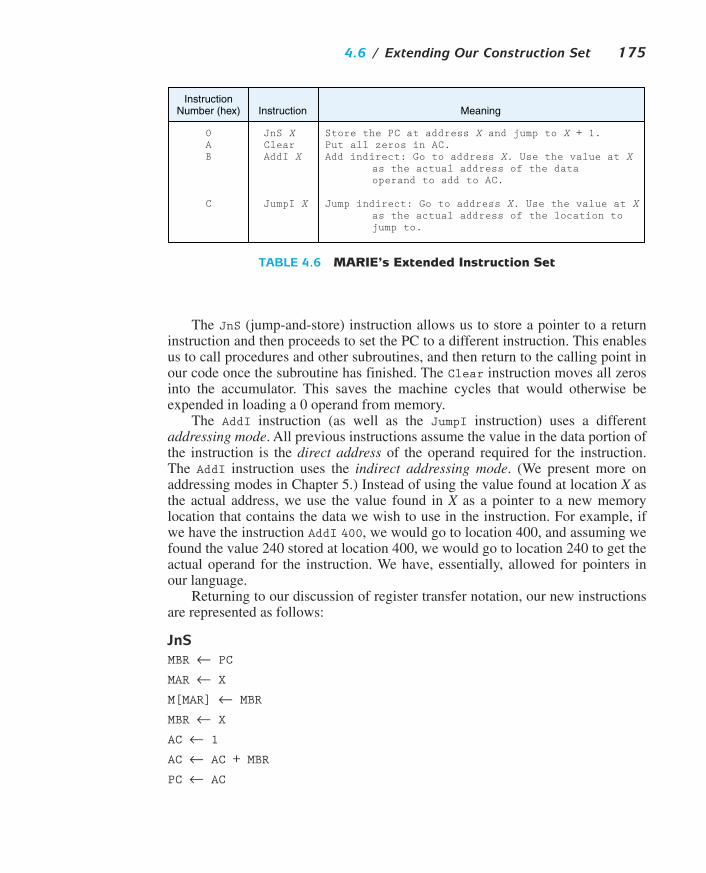
4.6 / Extending Our Construction Set 175
InstructionNumber (hex) Instruction
0AB
C
JnS XClearAddI X
JumpI X
Meaning
Store the PC at address X and jump to X + 1.Put all zeros in AC.Add indirect: Go to address X. Use the value at X
as the actual address of the dataoperand to add to AC.
Jump indirect: Go to address X. Use the value at Xas the actual address of the location tojump to.
TABLE 4.6 MARIE’s Extended Instruction Set
The JnS (jump-and-store) instruction allows us to store a pointer to a returninstruction and then proceeds to set the PC to a different instruction. This enablesus to call procedures and other subroutines, and then return to the calling point inour code once the subroutine has finished. The Clear instruction moves all zerosinto the accumulator. This saves the machine cycles that would otherwise beexpended in loading a 0 operand from memory.
The AddI instruction (as well as the JumpI instruction) uses a differentaddressing mode. All previous instructions assume the value in the data portion ofthe instruction is the direct address of the operand required for the instruction.The AddI instruction uses the indirect addressing mode. (We present more onaddressing modes in Chapter 5.) Instead of using the value found at location X asthe actual address, we use the value found in X as a pointer to a new memorylocation that contains the data we wish to use in the instruction. For example, ifwe have the instruction AddI 400, we would go to location 400, and assuming wefound the value 240 stored at location 400, we would go to location 240 to get theactual operand for the instruction. We have, essentially, allowed for pointers inour language.
Returning to our discussion of register transfer notation, our new instructionsare represented as follows:
JnS
MBR ← PC
MAR ← X
M[MAR] ← MBR
MBR ← X
AC ← 1
AC ← AC + MBR
PC ← AC

176 Chapter 4 / MARIE: An Introduction to a Simple Computer
Clear
AC ← 0
AddI X
MAR ← X
MBR ← M[MAR]
MAR ← MBR
MBR ← M[MAR]
AC ← AC + MBR
JumpI X
MAR ← X
MBR ← M[MAR]
PC ← MBR
Table 4.7 summarizes MARIE’s entire instruction set.
Let’s look at some examples using the full instruction set.
EXAMPLE 4.1 Here is an example using a loop to add five numbers:
Address Instruction Comments100 Load Addr /Load address of first number to be added101 Store Next /Store this address as our Next pointer102 Load Num /Load the number of items to be added103 Subt One /Decrement104 Store Ctr /Store this value in Ctr to control looping105 Clear /Clear AC
Loop, 106 Load Sum /Load the Sum into AC107 AddI Next /Add the value pointed to by location Next108 Store Sum /Store this Sum109 Load Next /Load Next10A Add One /Increment by one to point to next address10B Store Next /Store in our pointer Next10C Load Ctr /Load the loop control variable10D Subt One /Subtract one from the loop control variable10E Store Ctr /Store this new value in the loop control variable10F Skipcond 00 /If control variable < 0, skip next instruction110 Jump Loop /Otherwise, go to Loop111 Halt /Terminate program
Addr, 112 Hex 118 /Numbers to be summed start at location 118Next, 113 Hex 0 /A pointer to the next number to addNum, 114 Dec 5 /The number of values to addSum, 115 Dec 0 /The sumCtr, 116 Hex 0 /The loop control variableOne, 117 Dec 1 /Used to increment and decrement by 1

4.6 / Extending Our Construction Set 177
TABLE 4.7 MARIE’s Full Instruction Set
Opcode Instruction RTN
0000
0001
0010
0011
0100
0101
0110
0111
1000
1001
1010
1011
1100
JnS X
Load X
Store X
Add X
Subt X
Input
Output
Halt
Skipcond
Jump X
Clear
AddI X
JumpI X
MBR PCMAR XM[MAR] MBRMBR XAC 1AC AC + MBRPC AC
MAR XMBR M[MAR], AC MBR
MAR X, MBR ACM[MAR] MBR
MAR XMBR M[MAR]AC AC + MBR
MAR XMBR M[MAR]AC AC – MBR
AC InREG
OutREG AC
If IR[11—10] = 00 then If AC < 0 then PC PC + 1Else If IR[11—10] = 01 then If AC = 0 then PC PC + 1Else If IR[11—10] = 10 then If AC > 0 then PC PC + 1
PC IR[11—0]
AC 0
MAR XMBR M[MAR]MAR MBRMBR M[MAR]AC AC + MBR
MAR XMBR M[MAR]PC MBR

178 Chapter 4 / MARIE: An Introduction to a Simple Computer
118 Dec 10 /The values to be added together119 Dec 1511A Dec 2011B Dec 2511C Dec 30
Although the comments are reasonably explanatory, let’s walk through Exam-ple 4.1. Recall that the symbol table stores [label, location] pairs. The Load Addrinstruction becomes Load 112, because Addr is located at physical memory address112. The value of 118 (the value stored at Addr) is then stored in Next. This is thepointer that allows us to “step through” the five values we are adding (located ataddresses 118, 119, 11A, 11B, and 11C). The Ctr variable keeps track of howmany iterations of the loop we have performed. Since we are checking to see if Ctris negative to terminate the loop, we start by subtracting one from Ctr. Sum (withan initial value of 0) is then loaded in the AC. The loop begins, using Next as theaddress of the data we wish to add to the AC. The Skipcond statement terminatesthe loop when Ctr is negative by skipping the unconditional branch to the top ofthe loop. The program then terminates when the Halt statement is executed.
Example 4.2 shows how you can use the Skipcond and Jump instructions toperform selection. Although this example illustrates an if/else construct, youcan easily modify this to perform an if/then structure, or even a case (orswitch) structure.
EXAMPLE 4.2 This example illustrates the use of an if/else construct toallow for selection. In particular, it implements the following:
if X = Y thenX := X � 2
elseY := Y � X;
Address Instruction CommentsIf, 100 Load X /Load the first value
101 Subt Y /Subtract value of Y and store result in AC102 Skipcond 01 /If AC = 0, skip the next instruction103 Jump Else /Jump to the Else part if AC is not equal to 0
Then, 104 Load X /Reload X so it can be doubled105 Add X /Double X106 Store X /Store the new value107 Jump Endif /Skip over Else part to end of If
Else, 108 Load Y /Start the Else part by loading Y109 Subt X /Subtract X from Y10A Store Y /Store Y � X in Y

4.7 / A Discussion on Decoding: Hardwired vs. Microprogrammed Control 179
Endif, 10B Halt /Terminate program (it doesn’t do much!)X, 10C Dec 12 /Load the loop control variableY, 10D Dec 20 /Subtract one from the loop control variable
Example 4.3 demonstrates how JnS and JumpI are used to allow for subrou-tines. This program includes an END statement, another example of an assemblerdirective. This statement tells the assembler where the program ends. Otherpotential directives include statements to let the assembler know where to findthe first program instruction, how to set up memory, and whether blocks of codeare procedures.
EXAMPLE 4.3 This example illustrates the use of a simple subroutine to dou-ble any number and can be coded:
100 Load X /Load the first number to be doubled101 Store Temp /Use Temp as a parameter to pass value to Subr102 JnS Subr /Store return address, jump to procedure103 Store X /Store first number, doubled104 Load Y /Load the second number to be doubled105 Store Temp /Use Temp as a parameter to pass value to Subr106 JnS Subr /Store return address, jump to procedure107 Store Y /Store second number, doubled108 Halt /End program
X, 109 Dec 20Y, 10A Dec 48Temp, 10B Dec 0Subr, 10C Hex 0 /Store return address here
10D Clear /Clear AC as it was modified by JnS10E Load Temp /Actual subroutine to double numbers10F Add Temp /AC now holds double the value of Temp110 JumpI Subr /Return to calling code
END
Using MARIE’s simple instruction set, you should be able to implement anyhigh-level programming language construct, such as loop statements and whilestatements. These are left as exercises at the end of the chapter.
4.7 A DISCUSSION ON DECODING: HARDWIRED VS.MICROPROGRAMMED CONTROL
How does the control unit really function? We have done some hand waving andsimply assumed everything works as described, with a basic understanding that, foreach instruction, the control unit causes the CPU to execute a sequence of steps cor-rectly. In reality, there must be control signals to assert lines on various digital com-ponents to make things happen as described (recall the various digital components

180 Chapter 4 / MARIE: An Introduction to a Simple Computer
from Chapter 3). For example, when we perform an Add instruction in MARIE inassembly language, we assume the addition takes place because the control signalsfor the ALU are set to “add” and the result is put into the AC. The ALU has variouscontrol lines that determine which operation to perform. The question we need toanswer is, “How do these control lines actually become asserted?”
You can take one of two approaches to ensure control lines are set properly.The first approach is to physically connect all of the control lines to the actualmachine instructions. The instructions are divided up into fields, and different bitsin the instruction are combined through various digital logic components to drivethe control lines. This is called hardwired control, and is illustrated in Figure 4.14.
The control unit is implemented using hardware (with simple NAND gates,flip-flops, and counters, for example). We need a special digital circuit that uses,as inputs, the bits from the opcode field in our instructions, bits from the flag (orstatus) register, signals from the bus, and signals from the clock. It should pro-duce, as outputs, the control signals to drive the various components in the com-puter. For example, a 4-to-16 decoder could be used to decode the opcode. Byusing the contents of the IR register and the status of the ALU, this unit controlsthe registers, the ALU operations, all shifters, and bus access.
Instruction Register
Instruction Decoder
Control Unit(Combinational circuit)
Control Signals(These signals go to registers,
the bus and the ALU.)
Input from clock
Input from system bus(such as interrupts)
Input from status/flag registers
• • •
•••
• • •
••
••
••
FIGURE 4.14 Hardwired Control Unit

4.7 / A Discussion on Decoding: Hardwired vs. Microprogrammed Control 181
Instruction Register
MicroinstructionAddress Generation
Microinstruction Buffer
MicroinstructionDecoder
Control StoreMicroprogram Memory
Input from status/flag registers
•••
• • •
Put microinstructionin buffer
Subroutine that isexecuted for givenmicroinstruction
Select a specificinstruction
Clock
Control Signals
FIGURE 4.15 Microprogrammed Control
The advantage of hardwired control is that it is very fast. The disadvantage isthat the instruction set and the control logic are directly tied together by specialcircuits that are complex and difficult to design or modify. If someone designs ahardwired computer and later decides to extend the instruction set (as we did withMARIE), the physical components in the computer must be changed. This is pro-hibitively expensive, because not only must new chips be fabricated but also theold ones must e located and replaced.
The other approach, called microprogramming, uses software for control, andis illustrated in Figure 4.15.
All machine instructions are input into a special program, the microprogram,to convert the instruction into the appropriate control signals. The microprogramis essentially an interpreter, written in microcode, that is stored in firmware(ROM, PROM, or EPROM), which is often referred to as the control store. Thisprogram converts machine instructions of zeros and ones into control signals.

182 Chapter 4 / MARIE: An Introduction to a Simple Computer
Essentially there is one subroutine in this program for each machine instruction.The advantage of this approach is that if the instruction set requires modification,the microprogram is simply updated to match—no change is required in theactual hardware.
Microprogramming is flexible, simple in design, and lends itself to very pow-erful instruction sets. Microprogramming allows for convenient hardware/soft-ware tradeoffs: If what you want is not implemented in hardware (for example,your machine has no multiplication statement), it can be implemented in themicrocode. The disadvantage to this approach is that all instructions must gothrough an additional level of interpretation, slowing down the program execu-tion. In addition to this cost in time, there is a cost associated with the actualdevelopment, because appropriate tools are required. We discuss hardwired con-trol versus microprogramming in more detail in Chapter 9.
It is important to note that whether we are using hardwired control or micro-programmed control, timing is critical. The control unit is responsible for theactual timing signals that direct all data transfers and actions. These signals aregenerated in sequence with a simple binary counter. For example, the timing sig-nals for an architecture might include T1, T2, T3, T4, T5, T6, T7, and T8. These sig-nals control when actions can occur. A fetch for an instruction might occur onlywhen T1 is activated, whereas the fetch for an operand may occur only when T4 isactivated. We know that registers can change states only when the clock pulses,but they are also limited to changing in conjunction with a given timing signal.We saw an example of memory in Chapter 3 that included a Write Enable controlline. This control line could be ANDed with a timing signal to ensure that mem-ory only changed during specific intervals.
4.8 REAL WORLD EXAMPLES OF COMPUTER ARCHITECTURES
The MARIE architecture is designed to be as simple as possible so that the essentialconcepts of computer architecture would be easy to understand without being com-pletely overwhelming. Although MARIE’s architecture and assembly language arepowerful enough to solve any problems that could be carried out on a modernarchitecture using a high-level language such as C++, Ada, or Java, you probablywouldn’t be very happy with the inefficiency of the architecture or with how diffi-cult the program would be to write and to debug! MARIE’s performance could besignificantly improved if more storage were incorporated into the CPU by addingmore registers. Making things easier for the programmer is a different matter. Forexample, suppose a MARIE programmer wants to use procedures with parameters.Although MARIE allows for subroutines (programs can branch to various sectionsof code, execute the code, and then return), MARIE has no mechanism to supportthe passing of parameters. Programs can be written without parameters, but weknow that using them not only makes the program more efficient (particularly inthe area of reuse), but also makes the program easier to write and debug.
To allow for parameters, MARIE would need a stack, a data structure thatmaintains a list of items that can be accessed from only one end. A pile of platesin your kitchen cabinet is analogous to a stack: You put plates on the top and you
4.8 / Real World Examples of Computer Architectures 183
take plates off the top (normally). For this reason, stacks are often called last-in-first-out structures. (Please see Appendix A at the end of this book for a briefoverview of the various data structures.)
We can emulate a stack using certain portions of main memory if we restrictthe way data is accessed. For example, if we assume memory locations 0000through 00FF are used as a stack, and we treat 0000 as the top, then pushing(adding) onto the stack must be done from the top, and popping (removing) fromthe stack must be done from the top. If we push the value 2 onto the stack, it wouldbe placed at location 0000. If we then push the value 6, it would be placed at loca-tion 0001. If we then performed a pop operation, the 6 would be removed. A stackpointer keeps track of the location to which items should be pushed or popped.
MARIE shares many features with modern architectures but is not an accu-rate depiction of them. In the next two sections, we introduce two contemporarycomputer architectures to better illustrate the features of modern architecturesthat, in an attempt to follow Leonardo da Vinci’s advice, were excluded fromMARIE. We begin with the Intel architecture (the x86 and the Pentium families)and then follow with the MIPS architecture. We chose these architecturesbecause, although they are similar in some respects, they are built on fundamen-tally different philosophies. Each member of the x86 family of Intel architecturesis known as a CISC (Complex Instruction Set Computer) machine, whereas thePentium family and the MIPS architectures are examples of RISC (ReducedInstruction Set Computer) machines.
CISC machines have a large number of instructions, of variable length, withcomplex layouts. Many of these instructions are quite complicated, performingmultiple operations when a single instruction is executed (e.g., it is possible to doloops using a single assembly language instruction). The basic problem with CISCmachines is that a small subset of complex CISC instructions slows the systemsdown considerably. Designers decided to return to a less complicated architectureand to hardwire a small (but complete) instruction set that would execute extremelyquickly. This meant it would be the compiler’s responsibility to produce efficientcode for the ISA. Machines utilizing this philosophy are called RISC machines.
RISC is something of a misnomer. It is true that the number of instructions isreduced. However, the main objective of RISC machines is to simplify instruc-tions so they can execute more quickly. Each instruction performs only one oper-ation, they are all the same size, they have only a few different layouts, and allarithmetic operations must be performed between registers (data in memory can-not be used as operands). Virtually all new instruction sets (for any architectures)since 1982 have been RISC, or some sort of combination of CISC and RISC. Wecover CISC and RISC in detail in Chapter 9.
4.8.1 Intel Architectures
The Intel Corporation has produced many different architectures, some of whichmay be familiar to you. Intel’s first popular chip, the 8086, was introduced in1979 and used in the IBM PC computer. It handled 16-bit data and worked with20-bit addresses, thus it could address a million bytes of memory. (A close cousin

184 Chapter 4 / MARIE: An Introduction to a Simple Computer
of the 8086, the 8-bit 8088, was used in many PCs to lower the cost.) The 8086CPU was split into two parts: the execution unit, which included the general reg-isters and the ALU, and the bus interface unit, which included the instructionqueue, the segment registers, and the instruction pointer.
The 8086 had four 16-bit general purpose registers named AX (the primaryaccumulator), BX (the base register used to extend addressing), CX (the count reg-ister), and DX (the data register). Each of these registers was divided into twopieces: the most significant half was designated the “high” half (denoted by AH,BH, CH, and DH), and the least significant was designated the “low” half (denotedby AL, BL, CL, and DL). Various 8086 instructions required the use of a specificregister, but the registers could be used for other purposes as well. The 8086 alsohad three pointer registers: the stack pointer (SP), which was used as an offset intothe stack; the base pointer (BP), which was used to reference parameters pushedonto the stack; and the instruction pointer (IP), which held the address of the nextinstruction (similar to MARIE’s PC). There were also two index registers: the SI(source index) register, used as a source pointer for string operations, and the DI(destination index) register, used as a destination pointer for string operations. The8086 also had a status flags register. Individual bits in this register indicated vari-ous conditions, such as overflow, parity, carry interrupt, and so on.
An 8086 assembly language program was divided into different segments,special blocks or areas to hold specific types of information. There was a codesegment (for holding the program), a data segment (for holding the program’sdata), and a stack segment (for holding the program’s stack). To access informa-tion in any of these segments, it was necessary to specify that item’s offset fromthe beginning of the corresponding segment. Therefore, segment pointers werenecessary to store the addresses of the segments. These registers included the codesegment (CS) register, the data segment (DS) register, and the stack segment (SS)register. There was also a fourth segment register, called the extra segment (ES)register, which was used by some string operations to handle memory addressing.Addresses were specified using segment/offset addressing in the form: xxx:yyy,where xxx was the value in the segment register and yyy was the offset.
In 1980, Intel introduced the 8087, which added floating-point instructions tothe 8086 machine set as well as an 80-bit wide stack. Many new chips were intro-duced that used essentially the same ISA as the 8086, including the 80286 in1982 (which could address 16 million bytes) and the 80386 in 1985 (which couldaddress up to 4 billion bytes of memory). The 80386 was a 32-bit chip, the first ina family of chips often called IA-32 (for Intel Architecture, 32-bit). When Intelmoved from the 16-bit 80286 to the 32-bit 80386, designers wanted these archi-tectures to be backward compatible, which means that programs written for a lesspowerful and older processor should run on the newer, faster processors. Forexample, programs that ran on the 80286 should also run on the 80386. There-fore, Intel kept the same basic architecture and register sets. (New features wereadded to each successive model, so forward compatibility was not guaranteed.)
The naming convention used in the 80386 for the registers, which had gone from16 to 32 bits, was to include an “E” prefix (which stood for “extended”). So insteadof AX, BX, CX, and DX, the registers became EAX, EBX, ECX, and EDX. This

4.8 / Real World Examples of Computer Architectures 185
AH AL
EAX
AX
8 bits 8 bits16 bits
32 bits
FIGURE 4.16 The EAX Register, Broken into Parts
same convention was used for all other registers. However, the programmer couldstill access the original registers, AX, AL, and AH, for example, using the originalnames. Figure 4.16 illustrates how this worked, using the AX register as an example.
The 80386 and 80486 were both 32-bit machines, with 32-bit data buses. The80486 added a high-speed cache memory (see Chapter 6 for more details oncache and memory), which improved performance significantly.
The Pentium series (Intel changed the name from numbers such as 80486 to“Pentium” because it was unable to trademark the numbers) started with the Pen-tium processor, which had 32-bit registers and a 64-bit data bus and employed asuperscalar design. This means the CPU had multiple ALUs and could issuemore than one instruction per clock cycle (i.e., run instructions in parallel). ThePentium Pro added branch prediction, while the Pentium II added MMX technol-ogy (which most will agree was not a huge success) to deal with multimedia. ThePentium III added increased support for 3D graphics (using floating point instruc-tions). Historically, Intel used a classic CISC approach throughout its processorseries. The more recent Pentium II and III used a combined approach, employingCISC architectures with RISC cores that could translate from CISC to RISCinstructions. Intel was conforming to the current trend by moving away fromCISC and toward RISC.
The seventh generation family of Intel CPUs introduced the Intel Pentium 4(P4) processor. This processor differs from its predecessors in several ways, manyof which are beyond the scope of this text. Suffice it to say that the Pentium 4processor has clock rates of 1.4GHz (and higher), uses no less than 42 million tran-sistors for the CPU, and implements something called a “Netburst” microarchitec-ture. (The processors in the Pentium family, up to this point, had all been based onthe same microarchitecture, a term used to describe the architecture below theinstruction set.) This new microarchitecture is composed of several innovative tech-nologies, including a hyper-pipeline (we cover pipelines in Chapter 5), a 400MHz(and faster) system bus, and many refinements to cache memory and floating-pointoperations. This has made the P4 an extremely useful processor for multimediaapplications.
The introduction of the Itanium processor in 2001 marked Intel’s first 64-bitchip (IA-64). Itanium includes a register-based programming language and a veryrich instruction set. It also employs a hardware emulator to maintain backwardcompatibility with IA-32/x86 instruction sets. This processor has 4 integer units, 2floating point units, a significant amount of cache memory at 4 different levels (we

186 Chapter 4 / MARIE: An Introduction to a Simple Computer
study cache levels in Chapter 6), 128 floating point registers, 128 integer registers,and multiple miscellaneous registers for dealing with efficient loading of instruc-tions in branching situations. Itanium can address up to 16GB of main memory.
The assembly language of an architecture reveals significant informationabout that architecture. To compare MARIE’s architecture to Intel’s architecture,let’s return to Example 4.1, the MARIE program that used a loop to add five num-bers. Let’s rewrite the program in x86 assembly language, as seen in Example4.4. Note the addition of a Data segment directive and a Code segment directive.
EXAMPLE 4.4 A program using a loop to add five numbers written to run ona Pentium.
.DATANum1 EQU 10 ; Num1 is initialized to 10
EQU 15 ; Each word following Num1 is initializedEQU 20EQU 25EQU 30
Num DB 5 ; Initialize the loop counterSum DB 0 ; Initialize the Sum
.CODELEA EBX, Num1 ; Load the address of Num1 into EBXMOV ECX, Num ; Set the loop counterMOV EAX, 0 ; Initialize the sumMOV EDI, 0 ; Initialize the offset (of which number to add)
Start: ADD EAX, [EBX+EDI *4] ; Add the EBXth number to EAXINC EDI ; Increment the offset by 1DEC ECX ; Decrement the loop counter by 1JG Start ; If counter is greater than 0, return to StartMOV Sum, EAX ; Store the result in Sum
We can make the above program easier to read (which also makes it look lesslike MARIE’s assembly language) by using the loop statement. Syntactically, theloop instruction resembles a jump instruction, in that it requires a label. Theabove loop can be rewritten as follows:
MOV ECX, Num ; Set the counterStart: ADD EAX, [EBX + EDI + 4]
INC EDILOOP StartMOV Sum, EAX
The loop statement in x86 assembly is similar to the do...while construct inC, C++, or Java. The difference is that there is no explicit loop variable—the ECXregister is assumed to hold the loop counter. Upon execution of the loop instruc-

4.8 / Real World Examples of Computer Architectures 187
tion, the processor decreases ECX by one, and then tests ECX to see if it is equal tozero. If it is not zero, control jumps to Start; if it is zero, the loop terminates. Theloop statement is an example of the types of instructions that can be added to makethe programmer’s job easier, but which aren’t necessary for getting the job done.
4.8.2 MIPS Architectures
The MIPS family of CPUs has been one of the most successful and flexibledesigns of its class. The MIPS R3000, R4000, R5000, R8000, and R10000 aresome of the many registered trademarks belonging to MIPS Technologies, Inc.MIPS chips are used in embedded systems, in addition to computers (such as Sili-con Graphics machines) and various computerized toys (Nintendo and Sony usethe MIPS CPU in many of their products). Cisco, a very successful manufacturerof Internet routers, uses MIPS CPUs as well.
The first MIPS ISA was MIPS I, followed by MIPS II through MIPS V. Thecurrent ISAs are referred to as MIPS32 (for the 32-bit architecture) and MIPS64 (forthe 64-bit architecture). Our discussion in this section is focused on MIPS32. It isimportant to note that MIPS Technologies made a decision similar to that of Intel—as the ISA evolved, backward compatibility was maintained. And like Intel, eachnew version of the ISA included operations and instructions to improve efficiencyand handle floating point values. The new MIPS32 and MIPS64 architectures havesignificant improvements in VLSI technology and CPU organization. The end resultis notable cost and performance benefits over traditional architectures.
Like IA-32 and IA-64, the MIPS ISA embodies a rich set of instructions,including arithmetic, logical, comparison, data transfer, branching, jumping,shifting, and multimedia instructions. MIPS is a load/store architecture, whichmeans that all instructions (other than the load and store instructions) must useregisters as operands (no memory operands are allowed). MIPS32 has 168 32-bitinstructions, but many are similar. For example, there are six different addinstructions, all of which add numbers, but they vary in the operands and registersused. This idea of having multiple instructions for the same operation is commonin assembly language instruction sets. Another common instruction is the MIPSNOP (no-op) instruction, which does nothing except eat up time (NOPs are usedin pipelining as we see in Chapter 5).
The CPU in a MIPS32 architecture has 32 32-bit general purpose registersnumbered r0 through r31. (Two of these have special functions: r0 is hard-wired toa value of 0 and r31 is the default register for use with certain instructions, whichmeans it does not have to be specified in the instruction itself.) In MIPS assembly,these 32 general purpose registers are designated $0, $1, . . . , $31. Register 1 isreserved, and registers 26 and 27 are used by the operating system kernel. Registers28, 29, and 30 are pointer registers. The remaining registers can be referred to bynumber, using the naming convention shown in Table 4.8. For example, you canrefer to register 8 as $8 or as $t0.
There are two special purpose registers, HI and LO, which hold the results ofcertain integer operations. Of course, there is a PC (program counter) register aswell, giving a total of three special purpose registers.

188 Chapter 4 / MARIE: An Introduction to a Simple Computer
NamingConvention
RegisterNumber
$v0–$v1$a0–$a3$t0–$t7$s0–$s7$t8–$t9
2—34—78—1516—2324—25
Value Put in Register
Results, expressionsArgumentsTemporary valuesSaved valuesMore temporary values
TABLE 4.8 MIPS32 Register Naming Convention
MIPS32 has 32 32-bit floating point registers that can be used in single-preci-sion floating-point operations (with double-precision values being stored in even-odd pairs of these registers). There are 4 special-purpose floating-point controlregisters for use by the floating-point unit.
Let’s continue our comparison by writing the programs from Examples 4.1and 4.4 in MIPS32 assembly language.
EXAMPLE 4.5
. . ..data
# $t0 = sum# $t1 = loop counter Ctr
Value: .word 10, 15,20,25,30Sum = 0Ctr = 5.text.global main # declaration of main as a global variable
main: lw $t0, Sum # Initialize register containing sum to zerolw $t1, Ctr # Copy Ctr value to registerla $t2, value # $t2 is a pointer to current value
while: blez #t1, end_while # Done with loop if counter <= 0lw #t3, 0($t2) # Load value offset of 0 from pointeradd $t0, $t0, $t3 # Add value to sumaddi $t2, $t2, 4 # Go to next data valuesub #t1, $t1, 1 # Decrement Ctrb while # Return to top of loopla $t4, sum # Load the address of sum into registersw $t0, 0($t4) # Write the sum into memory location sum. . .
This is similar to the Intel code in that the loop counter is copied into a regis-ter, decremented during each interation of the loop, and then checked to see if it isless than or equal to zero. The register names may look formidable, but they areactually easy to work with once you understand the naming conventions.
Chapter Summary 189
If you are interested in writing MIPS programs, but don’t have a MIPSmachine, there are several simulators that you can use. The most popular is SPIM,a self-contained simulator for running MIPS R2000/R3000 assembly languageprograms. SPIM provides a simple debugger and implements almost the entire setof MIPS assembly instructions. The SPIM package includes source code and afull set of documentation. It is available for many flavors of Unix (includingLinux), Windows (PC), and Windows (DOS), as well as Macintosh. For furtherinformation, see the references at the end of this chapter.
If you examine Examples 4.1, 4.4, and 4.5, you will see that the instructionsare quite similar. Registers are referenced in different ways and have differentnames, but the underlying operations are basically the same. Some assembly lan-guages have larger instructions sets, allowing the programmer more choices forcoding various algorithms. But, as we have seen with MARIE, a large instructionset is not absolutely necessary to get the job done.
CHAPTER SUMMARY
This chapter has presented a simple architecture, MARIE, as a means to under-stand the basic fetch-decode-execute cycle and how computers actually oper-
ate. This simple architecture was combined with an ISA and an assemblylanguage, with emphasis given to the relationship between these two, allowing usto write programs for MARIE.
The CPU is the principal component in any computer. It consists of a data-path (registers and an ALU connected by a bus) and a control unit responsible forsequencing the operations and data movement and creating the timing signals. Allcomponents use these timing signals to work in unison. The input/output subsys-tem accommodates getting data into the computer and back out to the user.
MARIE is a very simple architecture designed specifically to illustrate theconcepts in this chapter without getting bogged down in too many technicaldetails. MARIE has 4K 16-bit words of main memory, uses 16-bit instructions,and has seven registers. There is only one general purpose register, the AC.Instructions for MARIE use 4 bits for the opcode and 12 bits for an address. Reg-ister transfer notation was introduced as a symbolic means for examining whateach instruction does at the register level.
The fetch-decode-execute cycle consists of the steps a computer follows torun a program. An instruction is fetched and then decoded, any required operandsare then fetched, and finally the instruction is executed. Interrupts are processedat the beginning of this cycle, returning to normal fetch-decode-execute statuswhen the interrupt handler is finished.
A machine language is a list of binary numbers representing executablemachine instructions, whereas an assembly language program uses symbolicinstructions to represent the numerical data from which the machine languageprogram is derived. Assembly language is a programming language, but does notoffer a large variety of data types or instructions for the programmer. Assemblylanguage programs represent a lower-level method of programming.

190 Chapter 4 / MARIE: An Introduction to a Simple Computer
You would probably agree that programming in MARIE’s assembly languageis, at the very least, quite tedious. We saw that most branching must be explicitlyperformed by the programmer, using jump and branch statements. It is also alarge step from this assembly language to a high-level language such as C++ orAda. However, the assembler is one step in the process of converting source codeinto something the machine can understand. We have not introduced assemblylanguage with the expectation that you will rush out and become an assembly lan-guage programmer. Rather, this introduction should serve to give you a betterunderstanding of machine architecture and how instructions and architectures arerelated. Assembly language should also give you a basic idea of what is going onbehind the scenes in high-level C++, Java, or Ada programs. Although assemblylanguage programs are easier to write for x86 and MIPS than for MARIE, all aremore difficult to write and debug than high-level language programs.
Intel and MIPS assembly languages and architectures were introduced (but byno means covered in detail) for two reasons. First, it is interesting to compare thevarious architectures, starting with a very simple architecture and continuing withmuch more complex and involved architectures. You should focus on the differ-ences as well as the similarities. Second, although the Intel and MIPS assemblylanguages looked different from MARIE’s assembly language, they are actuallyquite comparable. Instructions access memory and registers, and there are instruc-tions for moving data, performing arithmetic and logic operations, and branching.MARIE’s instruction set is very simple and lacks many of the “programmerfriendly” instructions that are present in both Intel and MIPS instruction sets. Inteland MIPS also have more registers than MARIE. Aside from the number ofinstructions and the number of registers, the languages function almost identically.
FURTHER READING
A MARIE assembly simulator is available on this textbook’s home page. Thissimulator assembles and executes your MARIE programs.
For more detailed information on CPU organization and ISAs, you arereferred to the Tanenbaum (1999) and Stallings (2000) books. Mano (1991) con-tains instructional examples of microprogrammed architectures. Wilkes (1958) isan excellent reference on microprogramming.
For more information regarding Intel assembly language programming,check out the Abel (2001), Dandamudi (1998), and Jones (1997) books. TheJones book takes a straightforward and simple approach to assembly languageprogramming, and all three books are quite thorough. If you are interested inother assembly languages, you might refer to Struble (1975) for IBM assembly,Gill, Corwin, and Logar (1987) for Motorola, and Sun Microsystems (1992) forSPARC. For a gentle introduction to embedded systems, try Williams (2000).
If you are interested in MIPS programming, Patterson and Hennessy (1997)give a very good presentation and their book has a separate appendix with usefulinformation. Donovan (1972) also has good coverage of the MIPS environment.Kane and Heinrich (1992) is the definitive text on the MIPS instruction set and

References 191
assembly language programming on MIPS machines. The MIPS home page alsohas a wealth of information.
To read more about Intel architectures, please refer to Alpert and Avnon(1993), Brey (2003), and Dulon (1998). Perhaps one of the best books on the sub-ject of the Pentium architecture is Shanley (1998). Motorola, UltraSparc, andAlpha architectures are discussed in Circello (1995), Horel and Lauterbach(1999), and McLellan (1995), respectively. For a more general introduction toadvanced architectures, see Tabak (1991).
If you wish to learn more about the SPIM simulator for MIPS, see Pattersonand Hennessy (1997) or the SPIM home page, which has documentation, manu-als, and various other downloads. Waldron (1999) is an excellent introduction toRISC assembly language programming and MIPS as well.
REFERENCES
Abel, Peter. IBM PC Assembly Language and Programming, 5th ed. Upper Saddle River, NJ: Pren-tice Hall, 2001.
Alpert, D., & Avnon, D. “Architecture of the Pentium Microprocessor,” IEEE Micro 13:3, April1993, pp. 11–21.
Brey, B. Intel Microprocessors 8086/8088, 80186/80188, 80286, 80386, 80486 Pentium, and Pen-tium Pro Processor, Pentium II, Pentium III, and Pentium IV: Architecture, Programming , andInterfacing, 6th ed. Englewood Cliffs, NJ: Prentice Hall, 2003.
Circello, J., Edgington, G., McCarthy, D., Gay, J., Schimke, D., Sullivan, S., Duerden, R., Hinds,C., Marquette, D., Sood, L., Crouch, A., & Chow, D. “The Superscalar Architecture of theMC68060,” IEEE Micro 15:2, April 1995, pp. 10–21.
Dandamudi, S. P. Introduction to Assembly Language Programming—From 8086 to PentiumProcessors, New York: Springer Verlag, 1998.
Donovan. J. J. Systems Programming, New York: McGraw-Hill, 1972.
Dulon, C. “The IA-64 Architecture at Work,” COMPUTER 31:7, July 1998, pp. 24–32.
Gill, A., Corwin, E., & Logar, A. Assembly Language Programming for the 68000, Upper SaddleRiver, NJ: Prentice Hall, 1987.
Goodman, J., & Miller, K. A Programmer’s View of Computer Architecture, Philadelphia: Saun-ders College Publishing, 1993.
Horel, T., & Lauterbach, G. “UltraSPARC III: Designing Third Generation 64-Bit Performance,”IEEE Micro 19:3, May/June 1999, pp. 73–85.
Jones, W. Assembly Language for the IBM PC Family, 2nd ed. El Granada, CA: Scott Jones, Inc., 1997.
Kane, G., & Heinrich, J., MIPS RISC Architecture, 2nd ed. Englewood Cliffs, NJ: Prentice Hall, 1992.
Mano, Morris. Digital Design, 2nd ed., Upper Saddle River, NJ: Prentice Hall, 1991.
McLellan, E. “The Alpha AXP Architecture and 21164 Alpha Microprocessor,” IEEE Micro 15:2,April 1995, pp. 33–43.
MIPS home page: www.mips.com
Patterson, D. A., & Hennessy, J. L. Computer Organization and Design: The Hardware/SoftwareInterface, 2nd ed. San Mateo, CA: Morgan Kaufmann, 1997.
Samaras, W. A., Cherukuri, N., & Venkataraman, S. “The IA-64 Itanium Processor Cartridge,”IEEE Micro 21:1, Jan/Feb 2001, pp. 82–89.