CHAPTER FIVE - Flip-Flops and Related Devicesmy.fit.edu/~vkepuska/Books/120244-0135123852_IM/Chp...
28
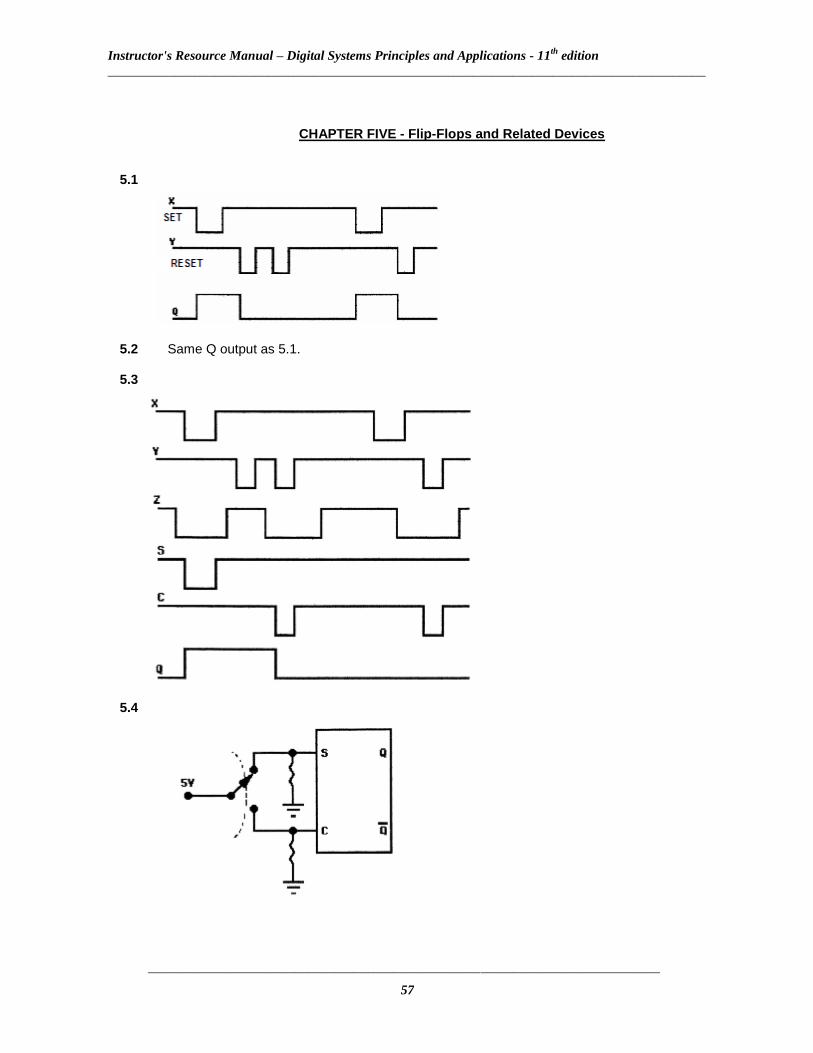
Instructor's Resource Manual – Digital Systems Principles and Applications - 11 th edition __________________________________________________________________________________________ _____________________________________________________________________________ 57 CHAPTER FIVE - Flip-Flops and Related Devices 5.1 5.2 Same Q output as 5.1. 5.3 5.4
Transcript of CHAPTER FIVE - Flip-Flops and Related Devicesmy.fit.edu/~vkepuska/Books/120244-0135123852_IM/Chp...
Instructor's Resource Manual – Digital Systems Principles and Applications - 11th
edition
__________________________________________________________________________________________
_____________________________________________________________________________
57
CHAPTER FIVE - Flip-Flops and Related Devices
5.1
5.2 Same Q output as 5.1. 5.3
5.4

Instructor's Resource Manual – Digital Systems Principles and Applications - 11th
edition
__________________________________________________________________________________________
_____________________________________________________________________________
58
5.5 One possibility:
5.6 The response shown would occur If the NAND latch is not working as a Flip-Flop. A permanent
logic HIGH at IC Z1-4 will prevent the latch from working properly and therefore the switch bounce will appear at Z1-6. When the 1 KHz squarewave is high, the switch bounce will be present at Z2-6.
5.7 Control inputs have to be stable for tS=20ns prior to the clock transition.
5.8 The FF will respond at times b, d, f, h, j corresponding to negative-going CLK transitions.
5.9 Assuming that Q=0 initially (for the positive edge triggered S-C FF).
Assuming that Q=0 initially (for the negative edge triggered S-C FF).
Instructor's Resource Manual – Digital Systems Principles and Applications - 11th
edition
__________________________________________________________________________________________
_____________________________________________________________________________
59
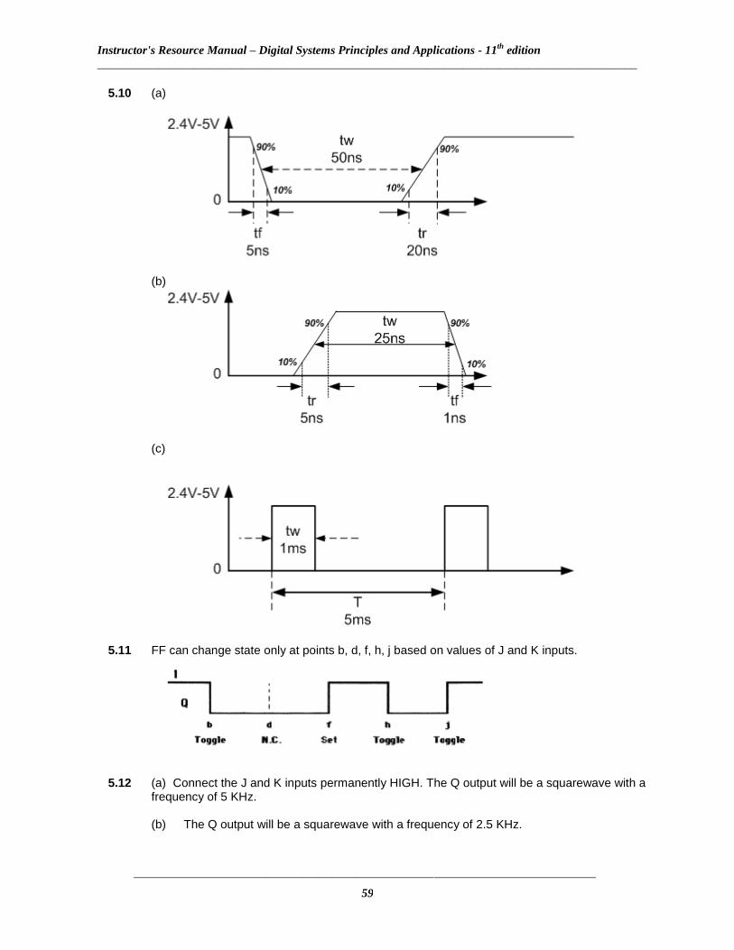
5.10 (a)
(b)
(c)
5.11 FF can change state only at points b, d, f, h, j based on values of J and K inputs.
5.12 (a) Connect the J and K inputs permanently HIGH. The Q output will be a squarewave with a
frequency of 5 KHz. (b) The Q output will be a squarewave with a frequency of 2.5 KHz.
Instructor's Resource Manual – Digital Systems Principles and Applications - 11th
edition
__________________________________________________________________________________________
_____________________________________________________________________________
60
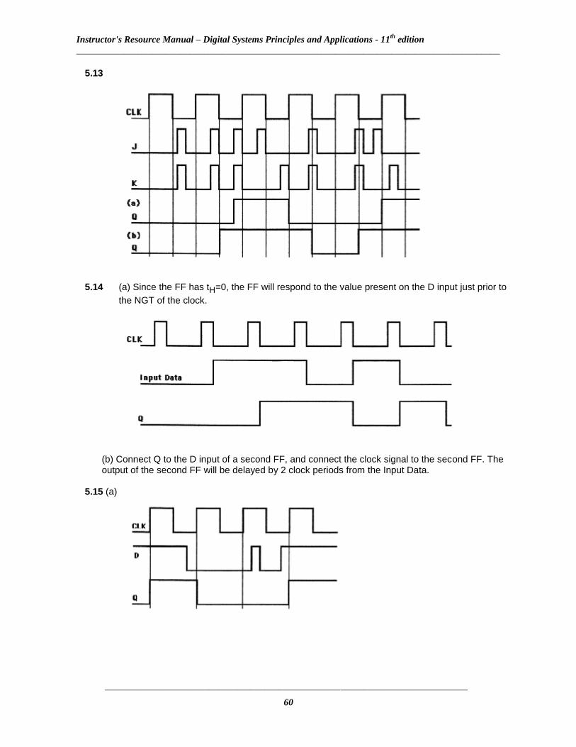
5.13
5.14 (a) Since the FF has tH=0, the FF will respond to the value present on the D input just prior to
the NGT of the clock.
(b) Connect Q to the D input of a second FF, and connect the clock signal to the second FF. The
output of the second FF will be delayed by 2 clock periods from the Input Data. 5.15 (a)

Instructor's Resource Manual – Digital Systems Principles and Applications - 11th
edition
__________________________________________________________________________________________
_____________________________________________________________________________
61
(b)
5.16 Q is a 500 Hz square wave. 5.17 (a)
(b)
5.18
Instructor's Resource Manual – Digital Systems Principles and Applications - 11th
edition
__________________________________________________________________________________________
_____________________________________________________________________________
62
5.19 If Q is connected back to D, the Q and Q outputs will oscillate while CLK is HIGH. This is
because Q =1 will produce S=0, C=1 which will make Q =0. This Q =0 then will make S=1,
C=0 which will make Q =1.
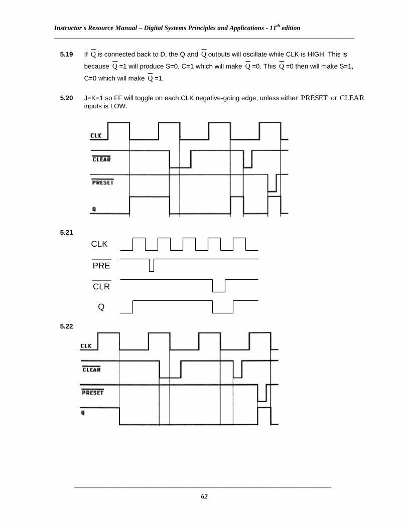
5.20 J=K=1 so FF will toggle on each CLK negative-going edge, unless either PRESET or CLEAR
inputs is LOW.
5.21
CLK
Q
____
CLR
____
PRE
5.22
Instructor's Resource Manual – Digital Systems Principles and Applications - 11th
edition
__________________________________________________________________________________________
_____________________________________________________________________________
63
5.23 (a) tpLH from CLK to Q is 200ns.
(b) With a tH = 5ns, the 7474 requires its control inputs to remain stable the longest time after
the CLK transition. With a tS = 60ns, the 74C74 requires its control inputs to remain stable the longest time before
the CLK transition.
(c) tW(L) at PRE is 30ns.
5.24 (a) tpHL, CLR-Q = 24ns (b) tpLH, PRE-CLR-Q = 41ns
(c) ns7.66MHz15
1
maxF
1Tmin
(d) tSU(min) = 25ns. No. There is insufficient time. (e) tpLH = 25ns CLR to Q 5.25
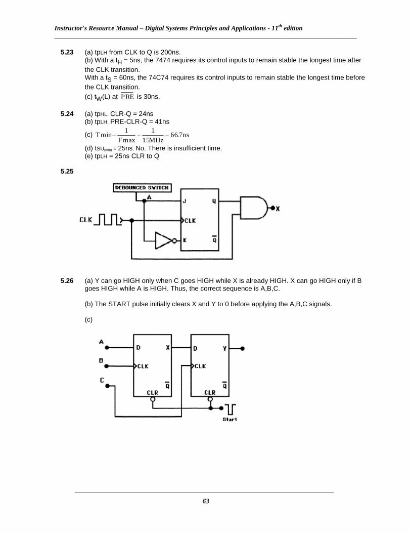
5.26 (a) Y can go HIGH only when C goes HIGH while X is already HIGH. X can go HIGH only if B goes HIGH while A is HIGH. Thus, the correct sequence is A,B,C.
(b) The START pulse initially clears X and Y to 0 before applying the A,B,C signals. (c)
Instructor's Resource Manual – Digital Systems Principles and Applications - 11th
edition
__________________________________________________________________________________________
_____________________________________________________________________________
64
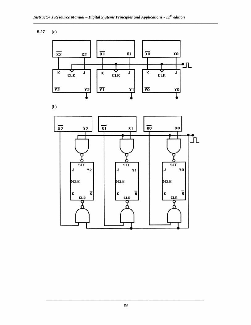
5.27 (a)
(b)
Instructor's Resource Manual – Digital Systems Principles and Applications - 11th
edition
__________________________________________________________________________________________
_____________________________________________________________________________
65
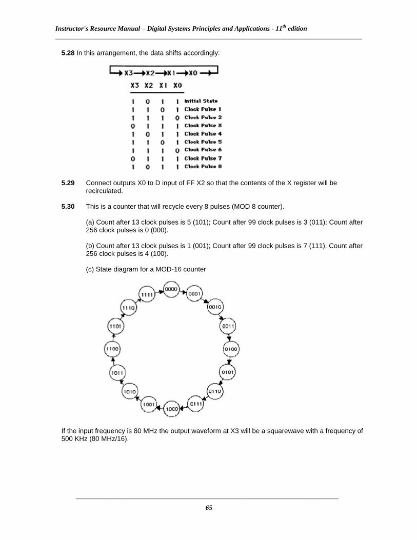
5.28 In this arrangement, the data shifts accordingly:
5.29 Connect outputs X0 to D input of FF X2 so that the contents of the X register will be
recirculated. 5.30 This is a counter that will recycle every 8 pulses (MOD 8 counter).
(a) Count after 13 clock pulses is 5 (101); Count after 99 clock pulses is 3 (011); Count after 256 clock pulses is 0 (000).
(b) Count after 13 clock pulses is 1 (001); Count after 99 clock pulses is 7 (111); Count after 256 clock pulses is 4 (100).
(c) State diagram for a MOD-16 counter
If the input frequency is 80 MHz the output waveform at X3 will be a squarewave with a frequency of 500 KHz (80 MHz/16).
Instructor's Resource Manual – Digital Systems Principles and Applications - 11th
edition
__________________________________________________________________________________________
_____________________________________________________________________________
66
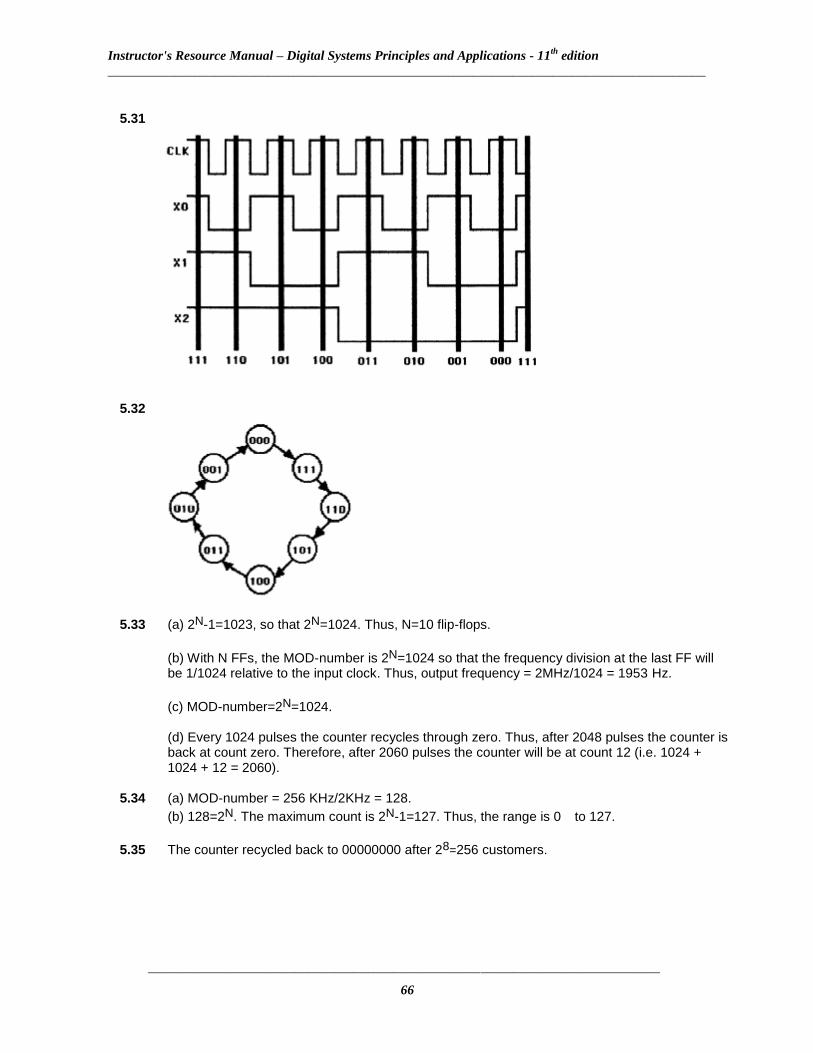
5.31
5.32
5.33 (a) 2N-1=1023, so that 2N=1024. Thus, N=10 flip-flops.
(b) With N FFs, the MOD-number is 2N=1024 so that the frequency division at the last FF will be 1/1024 relative to the input clock. Thus, output frequency = 2MHz/1024 = 1953 Hz.
(c) MOD-number=2N=1024. (d) Every 1024 pulses the counter recycles through zero. Thus, after 2048 pulses the counter is back at count zero. Therefore, after 2060 pulses the counter will be at count 12 (i.e. 1024 + 1024 + 12 = 2060).
5.34 (a) MOD-number = 256 KHz/2KHz = 128.
(b) 128=2N. The maximum count is 2N-1=127. Thus, the range is 0 to 127.
5.35 The counter recycled back to 00000000 after 28=256 customers.
Instructor's Resource Manual – Digital Systems Principles and Applications - 11th
edition
__________________________________________________________________________________________
_____________________________________________________________________________
67
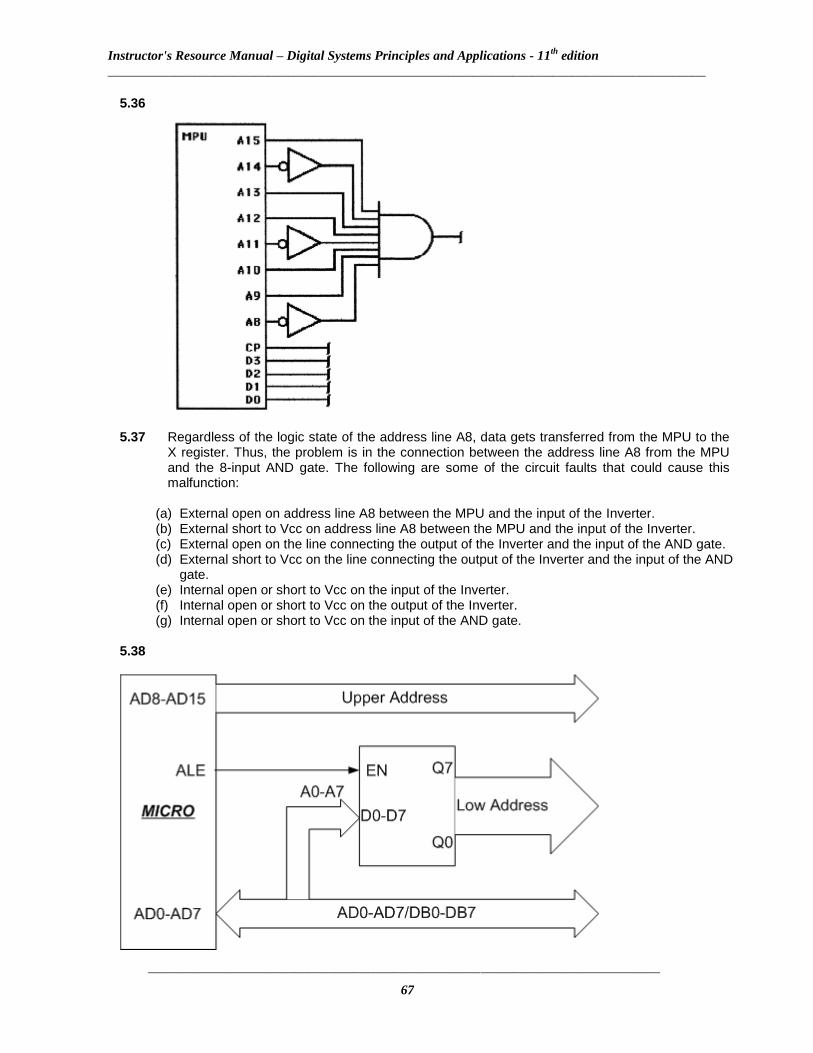
5.36
5.37 Regardless of the logic state of the address line A8, data gets transferred from the MPU to the X register. Thus, the problem is in the connection between the address line A8 from the MPU and the 8-input AND gate. The following are some of the circuit faults that could cause this malfunction:
(a) External open on address line A8 between the MPU and the input of the Inverter. (b) External short to Vcc on address line A8 between the MPU and the input of the Inverter. (c) External open on the line connecting the output of the Inverter and the input of the AND gate. (d) External short to Vcc on the line connecting the output of the Inverter and the input of the AND
gate. (e) Internal open or short to Vcc on the input of the Inverter. (f) Internal open or short to Vcc on the output of the Inverter. (g) Internal open or short to Vcc on the input of the AND gate.
5.38
Instructor's Resource Manual – Digital Systems Principles and Applications - 11th
edition
__________________________________________________________________________________________
_____________________________________________________________________________
68
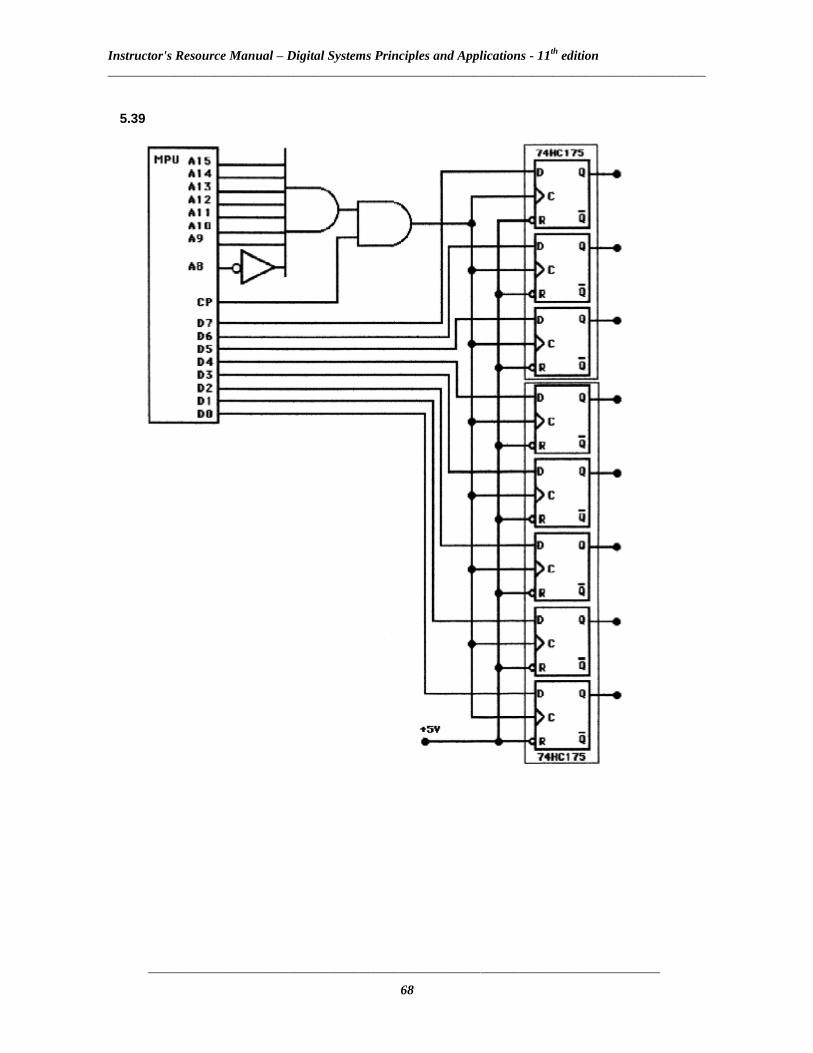
5.39
Instructor's Resource Manual – Digital Systems Principles and Applications - 11th
edition
__________________________________________________________________________________________
_____________________________________________________________________________
69
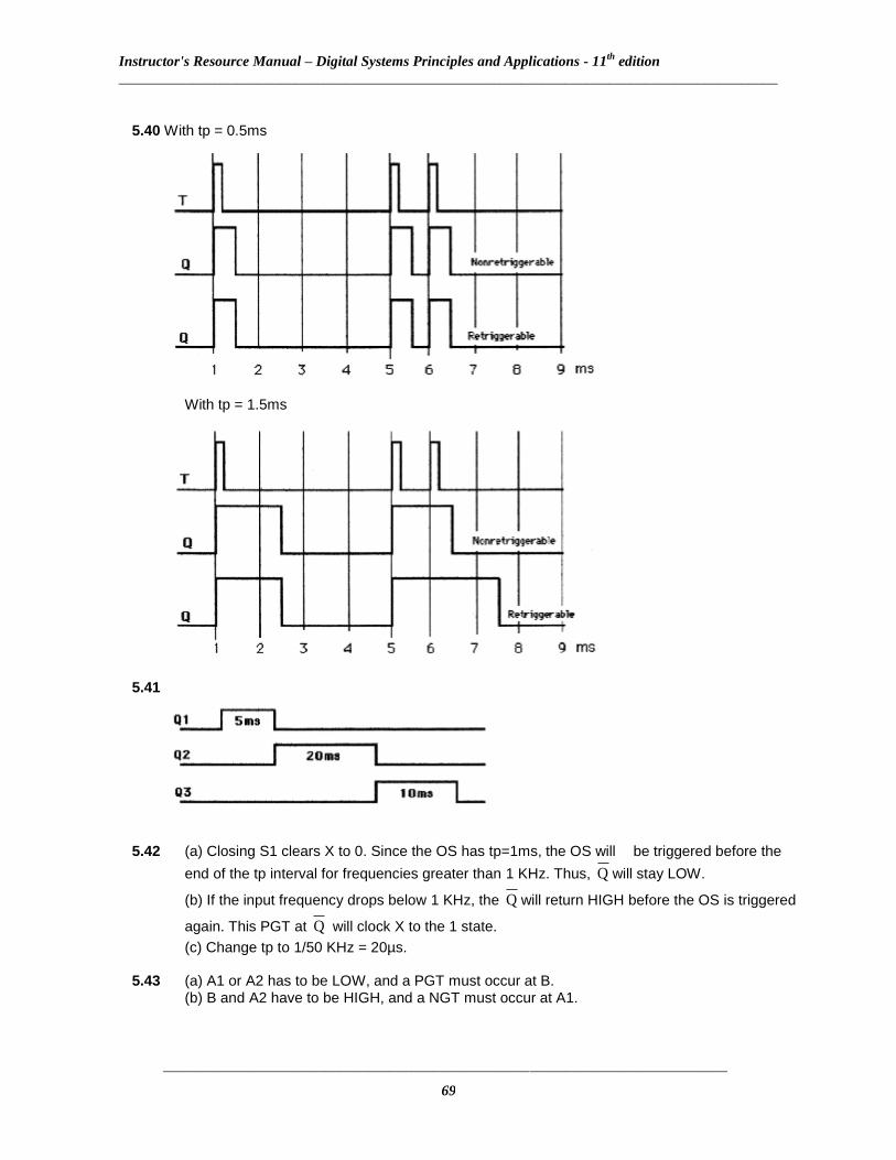
5.40 With tp = 0.5ms
With tp = 1.5ms
5.41
5.42 (a) Closing S1 clears X to 0. Since the OS has tp=1ms, the OS will be triggered before the
end of the tp interval for frequencies greater than 1 KHz. Thus, Q will stay LOW.
(b) If the input frequency drops below 1 KHz, the Q will return HIGH before the OS is triggered
again. This PGT at Q will clock X to the 1 state.
(c) Change tp to 1/50 KHz = 20µs. 5.43 (a) A1 or A2 has to be LOW, and a PGT must occur at B. (b) B and A2 have to be HIGH, and a NGT must occur at A1.
Instructor's Resource Manual – Digital Systems Principles and Applications - 11th
edition
__________________________________________________________________________________________
_____________________________________________________________________________
70
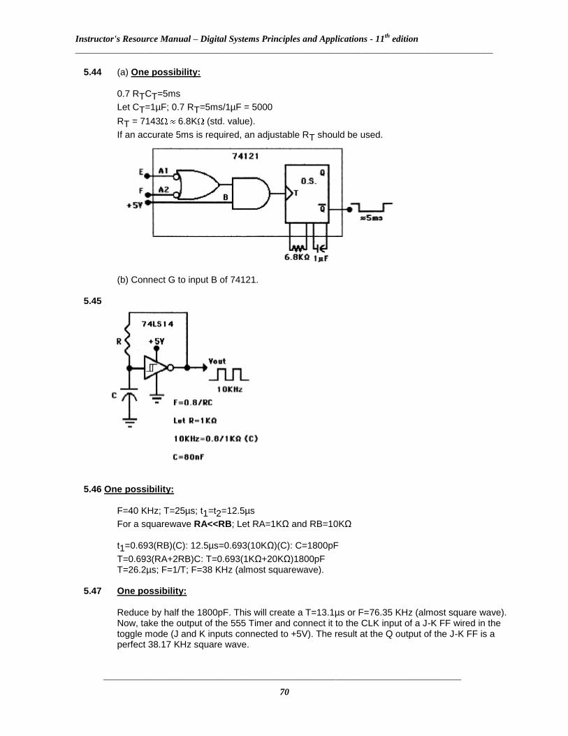
5.44 (a) One possibility: 0.7 RTCT=5ms
Let CT=1µF; 0.7 RT=5ms/1µF = 5000
RT = 7143 6.8K (std. value).
If an accurate 5ms is required, an adjustable RT should be used.
(b) Connect G to input B of 74121. 5.45
5.46 One possibility: F=40 KHz; T=25µs; t1=t2=12.5µs
For a squarewave RA<<RB; Let RA=1KΩ and RB=10KΩ t1=0.693(RB)(C): 12.5µs=0.693(10KΩ)(C): C=1800pF
T=0.693(RA+2RB)C: T=0.693(1KΩ+20KΩ)1800pF T=26.2µs; F=1/T; F=38 KHz (almost squarewave). 5.47 One possibility:
Reduce by half the 1800pF. This will create a T=13.1µs or F=76.35 KHz (almost square wave). Now, take the output of the 555 Timer and connect it to the CLK input of a J-K FF wired in the toggle mode (J and K inputs connected to +5V). The result at the Q output of the J-K FF is a perfect 38.17 KHz square wave.
Instructor's Resource Manual – Digital Systems Principles and Applications - 11th
edition
__________________________________________________________________________________________
_____________________________________________________________________________
71
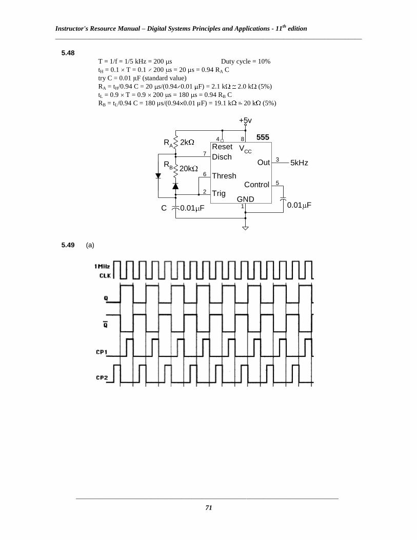
5.48
T = 1/f = 1/5 kHz = 200 s Duty cycle = 10%
tH = 0.1 T = 0.1 200 s = 20 s = 0.94 RA C
try C = 0.01 F (standard value)
RA = tH/0.94 C = 20 s/(0.94 0.01 F) = 2.1 k 2.0 k (5%)
tL = 0.9 T = 0.9 200 s = 180 s = 0.94 RB C
RB = tL/0.94 C = 180 s/(0.94 0.01 F) = 19.1 k 20 k (5%)
+5v
RA
RB
C
5kHz
0.01 F
Disch
Thresh
TrigGND
Reset VCC
Out
Control
55584
3
5
7
6
2
1
2k
20k
0.01 F
5.49 (a)
Instructor's Resource Manual – Digital Systems Principles and Applications - 11th
edition
__________________________________________________________________________________________
_____________________________________________________________________________
72
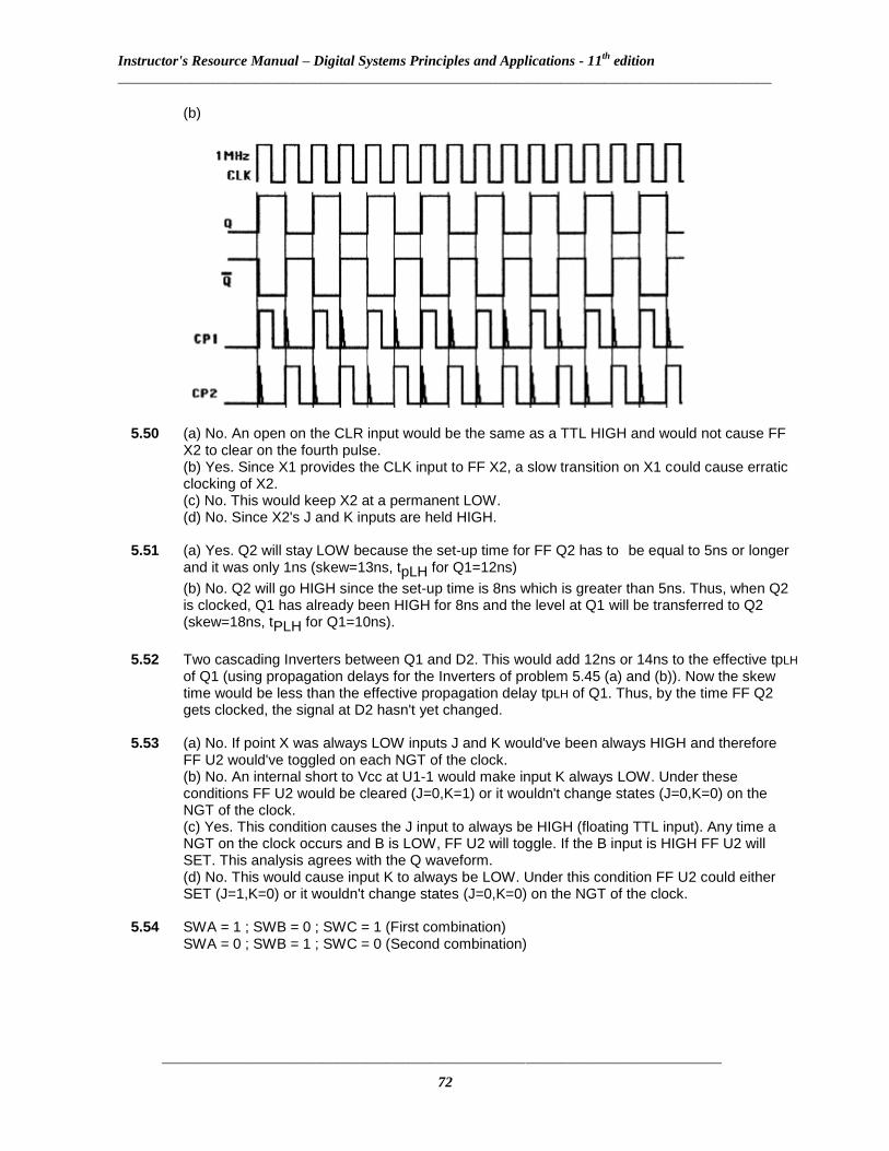
(b)
5.50 (a) No. An open on the CLR input would be the same as a TTL HIGH and would not cause FF
X2 to clear on the fourth pulse. (b) Yes. Since X1 provides the CLK input to FF X2, a slow transition on X1 could cause erratic clocking of X2.
(c) No. This would keep X2 at a permanent LOW. (d) No. Since X2's J and K inputs are held HIGH.
5.51 (a) Yes. Q2 will stay LOW because the set-up time for FF Q2 has to be equal to 5ns or longer
and it was only 1ns (skew=13ns, tpLH for Q1=12ns)
(b) No. Q2 will go HIGH since the set-up time is 8ns which is greater than 5ns. Thus, when Q2 is clocked, Q1 has already been HIGH for 8ns and the level at Q1 will be transferred to Q2 (skew=18ns, tPLH for Q1=10ns).
5.52 Two cascading Inverters between Q1 and D2. This would add 12ns or 14ns to the effective tpLH
of Q1 (using propagation delays for the Inverters of problem 5.45 (a) and (b)). Now the skew time would be less than the effective propagation delay tpLH of Q1. Thus, by the time FF Q2 gets clocked, the signal at D2 hasn't yet changed.
5.53 (a) No. If point X was always LOW inputs J and K would've been always HIGH and therefore
FF U2 would've toggled on each NGT of the clock. (b) No. An internal short to Vcc at U1-1 would make input K always LOW. Under these conditions FF U2 would be cleared (J=0,K=1) or it wouldn't change states (J=0,K=0) on the NGT of the clock. (c) Yes. This condition causes the J input to always be HIGH (floating TTL input). Any time a NGT on the clock occurs and B is LOW, FF U2 will toggle. If the B input is HIGH FF U2 will SET. This analysis agrees with the Q waveform. (d) No. This would cause input K to always be LOW. Under this condition FF U2 could either SET (J=1,K=0) or it wouldn't change states (J=0,K=0) on the NGT of the clock.
5.54 SWA = 1 ; SWB = 0 ; SWC = 1 (First combination) SWA = 0 ; SWB = 1 ; SWC = 0 (Second combination)
Instructor's Resource Manual – Digital Systems Principles and Applications - 11th
edition
__________________________________________________________________________________________
_____________________________________________________________________________
73
5.55 (a) No. Switch bounce would have no effect since the D inputs of the FFs are not sensitive to transitions.
(b) No. An open on the CLR (HIGH for TTL) input of FF Q2 wouldn't cause Q2 to change during a PGT on the CLK. (c) Yes. This fault would cause the switch bounce from the ENTER switch to be present at the CLK inputs of the D-type FFs. Since the input D of FF Q1 is at a logic LOW during the second combination, after the first bounce FF Q2 would get SET and after the second switch bounce it would get CLEAR.
5.56 (a) NAND or NOR gate latch. (b) Clocked J-K flip-flop. (c) D Latch. (d) Clocked D flip-flop or J-K flip-flop. (e) Clocked D flip-flop. (f) All types of flip-flops. (g) Any edge-triggered flip-flop. (h) J-K flip-flops. 5.57 (a) Asynchronous Inputs - Flip-flop inputs that can affect the operation of the flip-flop
independent of the synchronous and clock inputs. (b) Edge-Triggered - Manner in which a flip-flop is activated by a signal transition. It may be
either a positive or negative edge-triggered flip-flop. (c) Shift Register - Digital circuit that accepts binary data from some input source and then
shifts these data through a chain of flip-flops one bit at a time. (d) Frequency division - Expression normally associated with counters. The frequency
division ratio of a counter is equal to the total number of different states that counter can go through and is often referred to as the counter's MOD number.
(e) Asynchronous (Jam) Transfer - Data transfer performed without the aid of the clock. (f) State transition diagram - Way to show pictorially the states of flip-flops change with
each applied clock pulse. (g) Parallel Data Transfer - Operation by which the entire contents of a register are
transferred simultaneously to another register. (h) Serial Data Transfer - When data are transferred from one place to another one bit at a
time. (i) Retriggerable One-Shot - Type of One-Shot that can be triggered while it is in the quasi-
stable state, and it will begin a new tP interval.
(j) Schmitt-trigger inputs - Inputs on certain devices that accept slow-changing signals and produce oscillation-free transitions at the output.
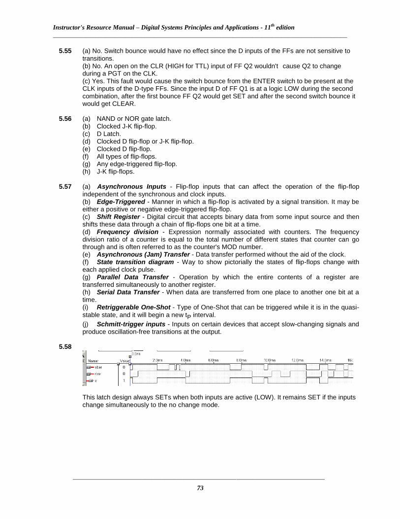
5.58
This latch design always SETs when both inputs are active (LOW). It remains SET if the inputs change simultaneously to the no change mode.

Instructor's Resource Manual – Digital Systems Principles and Applications - 11th
edition
__________________________________________________________________________________________
_____________________________________________________________________________
74
5.59
% SR Latch with active HIGH inputs
Run timing simulation
Digital Systems 11th ed
Tocci Widmer Moss %
SUBDESIGN prob5_59
( set, reset :INPUT;
q :OUTPUT; )
BEGIN
IF set == VCC THEN q = VCC; -- set or illegal command
ELSIF reset == VCC THEN q = GND; -- reset
ELSE q = q; -- hold
END IF;
END;
-- SR Latch with active HIGH inputs
-- Digital Systems 11th ed
-- Tocci Widmer Moss
ENTITY prob5_59 IS
PORT ( set, reset :IN BIT;
q :OUT BIT);
END prob5_59;
ARCHITECTURE behavior OF prob5_59 IS
BEGIN
PROCESS (set, reset)
BEGIN
IF set = '1' THEN q <= '1'; -- set or illegal command
ELSIF reset = '1' THEN q <= '0'; -- reset
END IF;
END PROCESS;
END behavior;
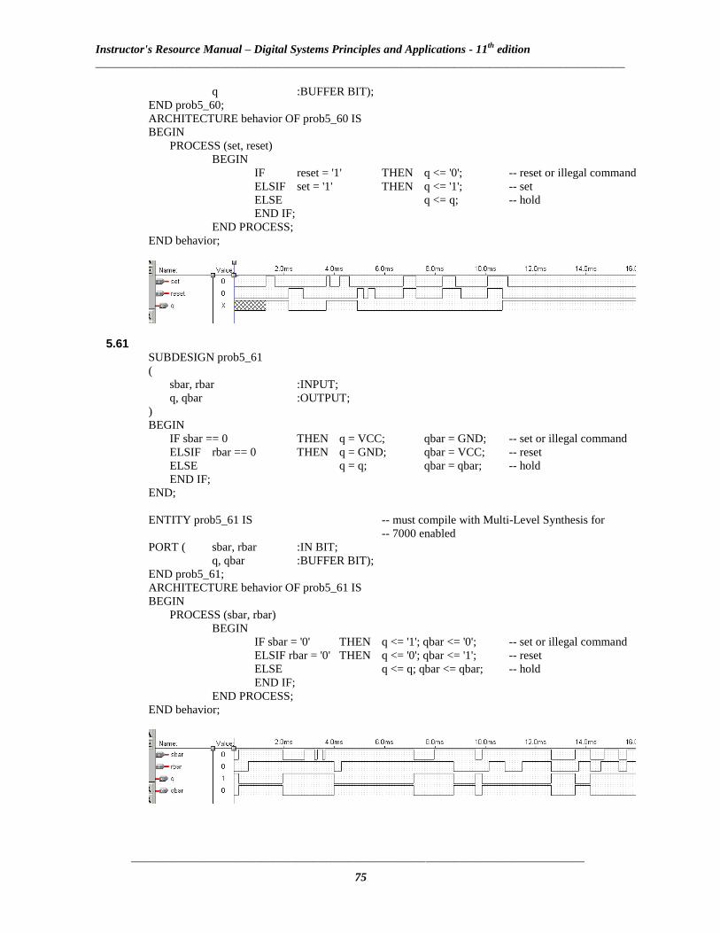
5.60 SUBDESIGN prob5_60
(
set, reset :INPUT;
q :OUTPUT;
)
BEGIN
IF reset == 1 THEN q = GND; -- reset or illegal command
ELSIF set == 1 THEN q = VCC; -- set
ELSE q = q; -- hold
END IF;
END;
ENTITY prob5_60 IS -- must compile with Multi-Level Synthesis for
-- 7000 enabled
PORT ( set, reset :IN BIT;
Instructor's Resource Manual – Digital Systems Principles and Applications - 11th
edition
__________________________________________________________________________________________
_____________________________________________________________________________
75
q :BUFFER BIT);
END prob5_60;
ARCHITECTURE behavior OF prob5_60 IS
BEGIN
PROCESS (set, reset)
BEGIN
IF reset = '1' THEN q <= '0'; -- reset or illegal command
ELSIF set = '1' THEN q <= '1'; -- set
ELSE q <= q; -- hold
END IF;
END PROCESS;
END behavior;
5.61 SUBDESIGN prob5_61
(
sbar, rbar :INPUT;
q, qbar :OUTPUT;
)
BEGIN
IF sbar == 0 THEN q = VCC; qbar = GND; -- set or illegal command
ELSIF rbar == 0 THEN q = GND; qbar = VCC; -- reset
ELSE q = q; qbar = qbar; -- hold
END IF;
END;
ENTITY prob5_61 IS -- must compile with Multi-Level Synthesis for
-- 7000 enabled
PORT ( sbar, rbar :IN BIT;
q, qbar :BUFFER BIT);
END prob5_61;
ARCHITECTURE behavior OF prob5_61 IS
BEGIN
PROCESS (sbar, rbar)
BEGIN
IF sbar = '0' THEN q <= '1'; qbar <= '0'; -- set or illegal command
ELSIF rbar = '0' THEN q <= '0'; qbar <= '1'; -- reset
ELSE q <= q; qbar <= qbar; -- hold
END IF;
END PROCESS;
END behavior;
Instructor's Resource Manual – Digital Systems Principles and Applications - 11th
edition
__________________________________________________________________________________________
_____________________________________________________________________________
76
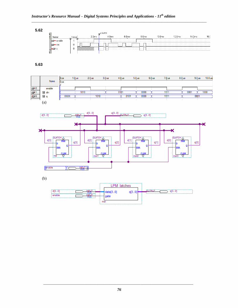
5.62
5.63
(a)
(b)
Instructor's Resource Manual – Digital Systems Principles and Applications - 11th
edition
__________________________________________________________________________________________
_____________________________________________________________________________
77
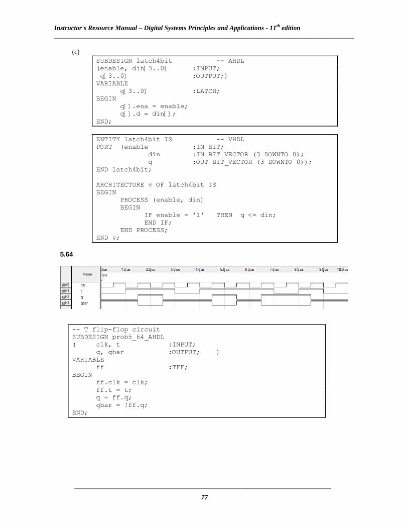
(c)
SUBDESIGN latch4bit -- AHDL
(enable, din[3..0] :INPUT;
q[3..0] :OUTPUT;)
VARIABLE
q[3..0] :LATCH;
BEGIN
q[].ena = enable;
q[].d = din[];
END;
ENTITY latch4bit IS -- VHDL
PORT (enable :IN BIT;
din :IN BIT_VECTOR (3 DOWNTO 0);
q :OUT BIT_VECTOR (3 DOWNTO 0));
END latch4bit;
ARCHITECTURE v OF latch4bit IS
BEGIN
PROCESS (enable, din)
BEGIN
IF enable = '1' THEN q <= din;
END IF;
END PROCESS;
END v;
5.64
-- T flip-flop circuit
SUBDESIGN prob5_64_AHDL
( clk, t :INPUT;
q, qbar :OUTPUT; )
VARIABLE
ff :TFF;
BEGIN
ff.clk = clk;
ff.t = t;
q = ff.q;
qbar = !ff.q;
END;
Instructor's Resource Manual – Digital Systems Principles and Applications - 11th
edition
__________________________________________________________________________________________
_____________________________________________________________________________
78
-- T flip-flop circuit
ENTITY prob5_64_VHDL IS
PORT ( clk, t :IN BIT;
q, qbar :OUT BIT);
END prob5_64_VHDL;
ARCHITECTURE vhdl OF prob5_64_VHDL IS
SIGNAL qstate :BIT;
BEGIN
PROCESS (clk)
BEGIN
IF clk'EVENT AND clk = '1' THEN
IF t = '1' THEN
qstate <= NOT qstate;
END IF;
END IF;
END PROCESS;
q <= qstate;
qbar <= NOT qstate;
END vhdl;
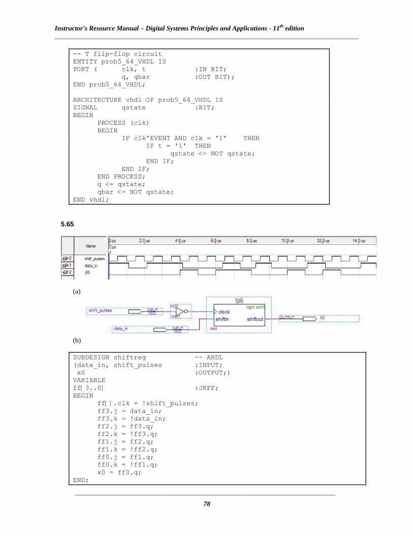
5.65
(a)
(b)
SUBDESIGN shiftreg -- AHDL
(data_in, shift_pulses :INPUT;
x0 :OUTPUT;)
VARIABLE
ff[3..0] :JKFF;
BEGIN
ff[].clk = !shift_pulses;
ff3.j = data_in;
ff3.k = !data_in;
ff2.j = ff3.q;
ff2.k = !ff3.q;
ff1.j = ff2.q;
ff1.k = !ff2.q;
ff0.j = ff1.q;
ff0.k = !ff1.q;
x0 = ff0.q;
END;
Instructor's Resource Manual – Digital Systems Principles and Applications - 11th
edition
__________________________________________________________________________________________
_____________________________________________________________________________
79
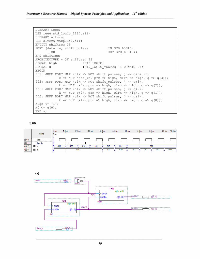
LIBRARY ieee;
USE ieee.std_logic_1164.all;
LIBRARY altera;
USE altera.maxplus2.all;
ENTITY shiftreg IS
PORT (data_in, shift_pulses :IN STD_LOGIC;
x0 :OUT STD_LOGIC);
END shiftreg;
ARCHITECTURE v OF shiftreg IS
SIGNAL high :STD_LOGIC;
SIGNAL q :STD_LOGIC_VECTOR (3 DOWNTO 0);
BEGIN
ff3: JKFF PORT MAP (clk => NOT shift_pulses, j => data_in,
k => NOT data_in, prn => high, clrn => high, q => q(3));
ff2: JKFF PORT MAP (clk => NOT shift_pulses, j => q(3),
k => NOT q(3), prn => high, clrn => high, q => q(2));
ff1: JKFF PORT MAP (clk => NOT shift_pulses, j => q(2),
k => NOT q(2), prn => high, clrn => high, q => q(1));
ff0: JKFF PORT MAP (clk => NOT shift_pulses, j => q(1),
k => NOT q(1), prn => high, clrn => high, q => q(0));
high <= '1';
x0 <= q(0);
END v;
5.66
(a)
Instructor's Resource Manual – Digital Systems Principles and Applications - 11th
edition
__________________________________________________________________________________________
_____________________________________________________________________________
80
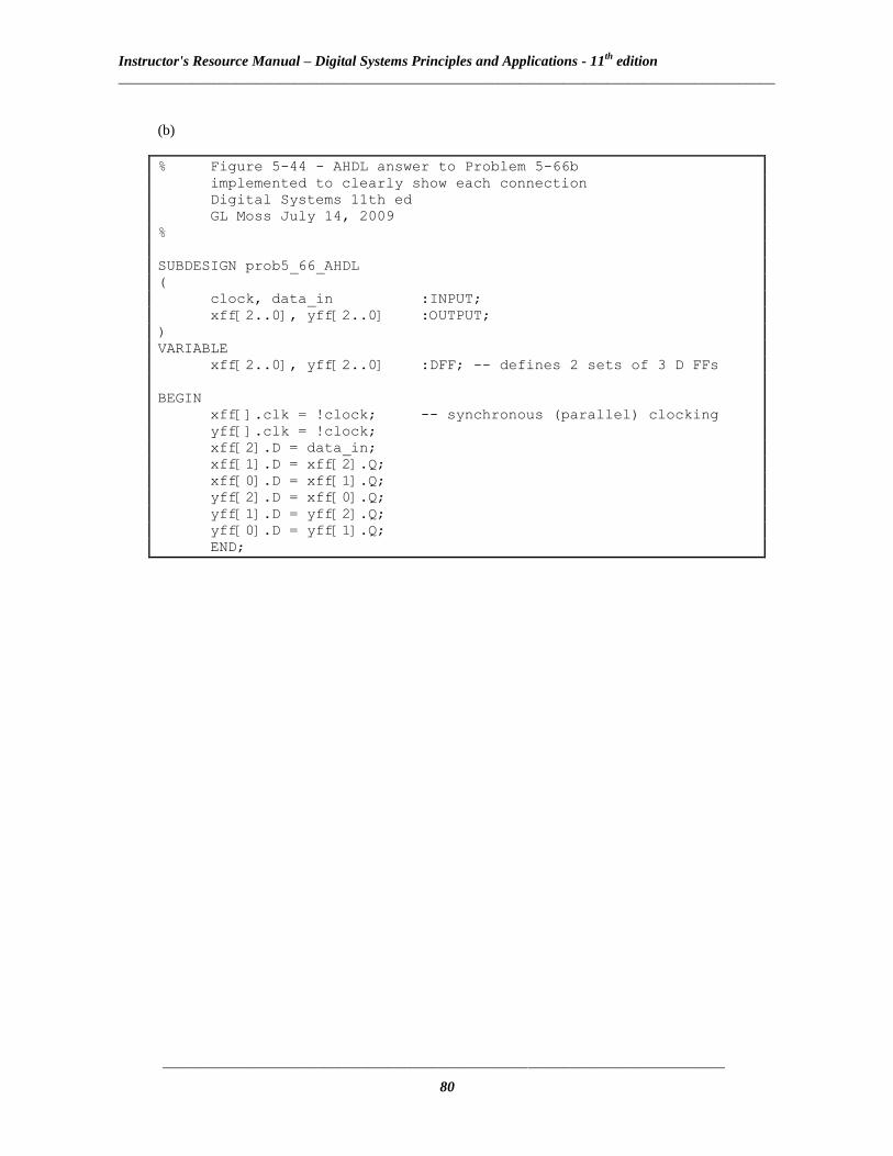
(b)
% Figure 5-44 - AHDL answer to Problem 5-66b
implemented to clearly show each connection
Digital Systems 11th ed
GL Moss July 14, 2009
%
SUBDESIGN prob5_66_AHDL
(
clock, data_in :INPUT;
xff[2..0], yff[2..0] :OUTPUT;
)
VARIABLE
xff[2..0], yff[2..0] :DFF; -- defines 2 sets of 3 D FFs
BEGIN
xff[].clk = !clock; -- synchronous (parallel) clocking
yff[].clk = !clock;
xff[2].D = data_in;
xff[1].D = xff[2].Q;
xff[0].D = xff[1].Q;
yff[2].D = xff[0].Q;
yff[1].D = yff[2].Q;
yff[0].D = yff[1].Q;
END;
Instructor's Resource Manual – Digital Systems Principles and Applications - 11th
edition
__________________________________________________________________________________________
_____________________________________________________________________________
81
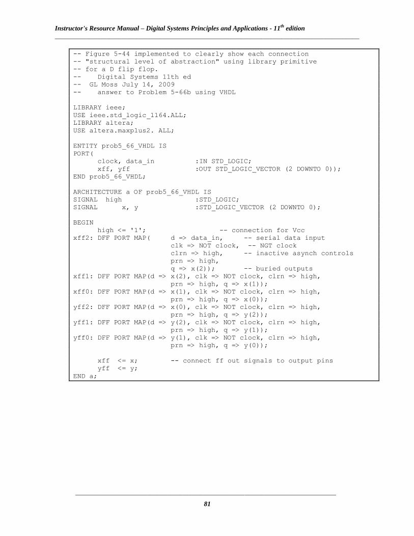
-- Figure 5-44 implemented to clearly show each connection
-- "structural level of abstraction" using library primitive
-- for a D flip flop.
-- Digital Systems 11th ed
-- GL Moss July 14, 2009
-- answer to Problem 5-66b using VHDL
LIBRARY ieee;
USE ieee.std_logic_1164.ALL;
LIBRARY altera;
USE altera.maxplus2. ALL;
ENTITY prob5_66_VHDL IS
PORT(
clock, data_in :IN STD_LOGIC;
xff, yff :OUT STD_LOGIC_VECTOR (2 DOWNTO 0));
END prob5_66_VHDL;
ARCHITECTURE a OF prob5_66_VHDL IS
SIGNAL high :STD_LOGIC;
SIGNAL x, y :STD_LOGIC_VECTOR (2 DOWNTO 0);
BEGIN
high <= '1'; -- connection for Vcc
xff2: DFF PORT MAP( d => data_in, -- serial data input
clk => NOT clock, -- NGT clock
clrn => high, -- inactive asynch controls
prn => high,
q => x(2)); -- buried outputs
xff1: DFF PORT MAP(d => x(2), clk => NOT clock, clrn => high,
prn => high, q => x(1));
xff0: DFF PORT MAP(d => x(1), clk => NOT clock, clrn => high,
prn => high, q => x(0));
yff2: DFF PORT MAP(d => x(0), clk => NOT clock, clrn => high,
prn => high, q => y(2));
yff1: DFF PORT MAP(d => y(2), clk => NOT clock, clrn => high,
prn => high, q => y(1));
yff0: DFF PORT MAP(d => y(1), clk => NOT clock, clrn => high,
prn => high, q => y(0));
xff <= x; -- connect ff out signals to output pins
yff <= y;
END a;
Instructor's Resource Manual – Digital Systems Principles and Applications - 11th
edition
__________________________________________________________________________________________
_____________________________________________________________________________
82
5.67 (a) % Figure 5-57 implemented to clearly show each connection %
SUBDESIGN prob5_67a
(
clock1, xin :INPUT;
q1, q2 :OUTPUT;
)
VARIABLE
q1, q2 :DFF; -- defines two D FFs
clock2, nandout :node;
BEGIN
q1 . clk = !clock1;
q1 . d = VCC;
q2 . d = q[1] . q;
clock2 = !nandout;
nandout = !(xin & clock1);
END;
5.67 (b) --Answer to problem (b)
LIBRARY ieee;
USE ieee.std_logic_1164.ALL;
LIBRARY altera;
USE altera.maxplus2. ALL;
ENTITY prob5_67b IS
PORT(
clock1, xin :IN std_logic ;
q1, q2 :OUT std_logic);
END prob5_67b;
ARCHITECTURE a OF prob5_67b IS
SIGNAL high, clock2, nandout, clk1not, clk2not :std_logic;
SIGNAL qone, qtwo :std_logic;
BEGIN
high <= '1'; -- connection for Vcc
nandout <= NOT (xin AND clock1);
clock2 <= NOT nandout;
clock2not <= NOT clock2;
clocknot <= NOT clock1;
ff1: DFF
PORT MAP ( d => high,
clk => clk1not,
clrn => high,
prn => high,
q => qone);
ff2: DFF
PORT MAP ( d => qone,
clk => clk2not,
clrn => high,
prn => high,
q => qtwo);
q1 <= qone; -- connect ff out signals to output pins
q2 <= qtwo;
END a;
Instructor's Resource Manual – Digital Systems Principles and Applications - 11th
edition
__________________________________________________________________________________________
_____________________________________________________________________________
83
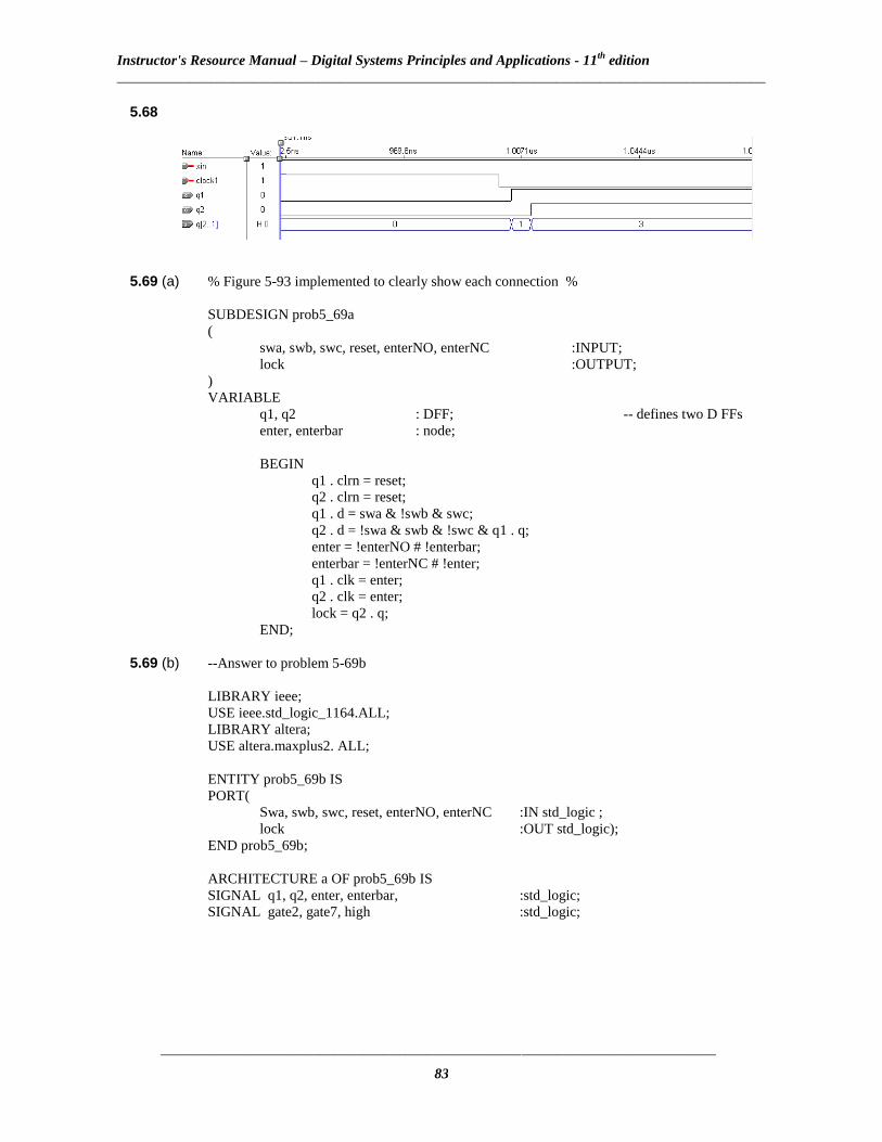
5.68
5.69 (a) % Figure 5-93 implemented to clearly show each connection %
SUBDESIGN prob5_69a
(
swa, swb, swc, reset, enterNO, enterNC :INPUT;
lock :OUTPUT;
)
VARIABLE
q1, q2 : DFF; -- defines two D FFs
enter, enterbar : node;
BEGIN
q1 . clrn = reset;
q2 . clrn = reset;
q1 . d = swa & !swb & swc;
q2 . d = !swa & swb & !swc & q1 . q;
enter = !enterNO # !enterbar;
enterbar = !enterNC # !enter;
q1 . clk = enter;
q2 . clk = enter;
lock = q2 . q;
END;
5.69 (b) --Answer to problem 5-69b
LIBRARY ieee;
USE ieee.std_logic_1164.ALL;
LIBRARY altera;
USE altera.maxplus2. ALL;
ENTITY prob5_69b IS
PORT(
Swa, swb, swc, reset, enterNO, enterNC :IN std_logic ;
lock :OUT std_logic);
END prob5_69b;
ARCHITECTURE a OF prob5_69b IS
SIGNAL q1, q2, enter, enterbar, :std_logic;
SIGNAL gate2, gate7, high :std_logic;
Instructor's Resource Manual – Digital Systems Principles and Applications - 11th
edition
__________________________________________________________________________________________
_____________________________________________________________________________
84
BEGIN
high <= '1'; -- connection for Vcc
gate2 <= swa AND (NOT swb) AND swc;
gate7 <= (NOT swa) AND swb AND (NOT swc) AND q1;
lock <= q2;
enter <= NOT enterNO OR NOT enterbar;
enterbar <= NOT enterNC OR NOT enter;
ff1: DFF
PORT MAP ( d => gate2,
clk => enter,
clrn => reset,
prn => high,
q => q1);
ff2: DFF
PORT MAP ( d => gate7, -- toggle mode
clk => enter, -- ripple clock connection
clrn => reset, -- asynch inputs inactive
prn => high,
q => q2);
END a;