Chapter 8. Current Source & Bias Circuiticlab.hanyang.ac.kr/research/data/DLL Design Examples,...
56
Changsik Yoo @ DRAM Design 4, Samsung Electronics 1 IC Design Education Center Delay-Locked Loop - Design Examples, Design Issues/Tips
-
Upload
trinhkhanh -
Category
Documents
-
view
222 -
download
2
Transcript of Chapter 8. Current Source & Bias Circuiticlab.hanyang.ac.kr/research/data/DLL Design Examples,...
Changsik Yoo @ DRAM Design 4, Samsung Electronics 1
IC Design Education Center
Delay-Locked Loop- Design Examples, Design Issues/Tips

Changsik Yoo @ DRAM Design 4, Samsung Electronics 2
Agenda• Introduction• Building blocks of DLL• Design issues of DLL• DLL examples• Design examples
– DLL for DDR SDRAM – DLL for direct RDRAM
• Summary
Changsik Yoo @ DRAM Design 4, Samsung Electronics 3
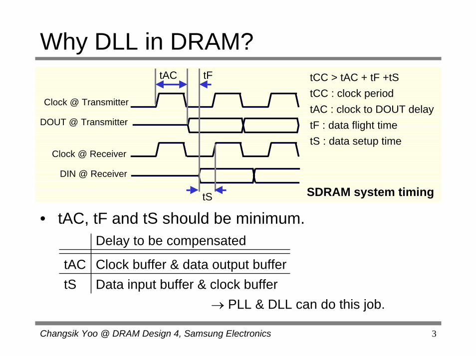
Why DLL in DRAM?tAC tF
tS SDRAM system timing
Clock @ Transmitter
Clock @ Receiver
DOUT @ Transmitter
DIN @ Receiver
tCC > tAC + tF +tStCC : clock periodtAC : clock to DOUT delaytF : data flight timetS : data setup time
• tAC, tF and tS should be minimum.Delay to be compensated
tAC Clock buffer & data output buffertS Data input buffer & clock buffer
→ PLL & DLL can do this job.

Changsik Yoo @ DRAM Design 4, Samsung Electronics 4
Is DLL better than PLL for DRAM?
• Yes !!!– Frequency multiplication is not necessary.– There is no jitter accumulation in DLL.– DLL is a first-order system.
- Inherently stable- Parasitic pole due to the feedback delay exists and thusthe stability should be considered as well.
Changsik Yoo @ DRAM Design 4, Samsung Electronics 5
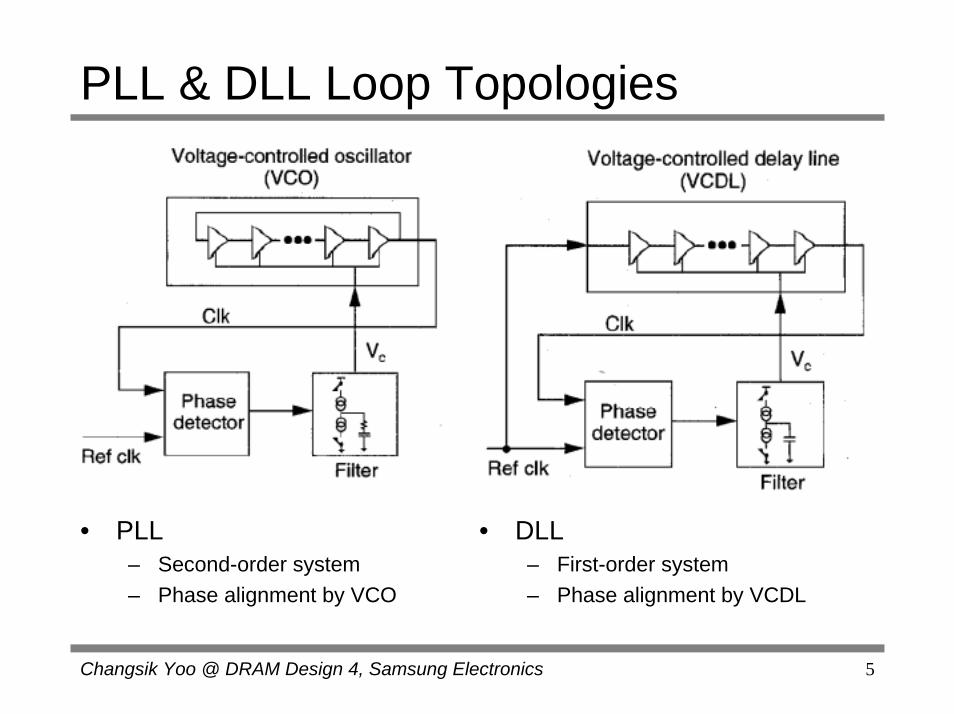
PLL & DLL Loop Topologies
• PLL– Second-order system– Phase alignment by VCO
• DLL– First-order system– Phase alignment by VCDL

Changsik Yoo @ DRAM Design 4, Samsung Electronics 6
Transient Response to Supply StepRef. IEEE Micro’98
• Jitter of VCO accumulates until the loop feedback’s correcting action takes effect.
• VCDL in DLL ; no jitter accumulation

Changsik Yoo @ DRAM Design 4, Samsung Electronics 7
Delay Locked Loop
Ext. Clock
Int. Clock
Data from Array
d1 + d2d1 tCC - (d1 + d2)
Variable Delay Line
PD
CompensationDelay
LPF
DOUTBuffer
Ext. Data
d2

Changsik Yoo @ DRAM Design 4, Samsung Electronics 8
Agenda• Introduction• Building blocks of DLL• Design issues of DLL• DLL examples• Design examples
– DLL for DDR SDRAM – DLL for direct RDRAM
• Summary
Changsik Yoo @ DRAM Design 4, Samsung Electronics 9
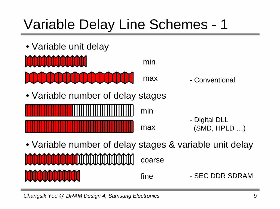
Variable Delay Line Schemes - 1• Variable unit delay
min
max - Conventional
• Variable number of delay stagesmin
- Digital DLL(SMD, HPLD …)max
• Variable number of delay stages & variable unit delay coarse
fine - SEC DDR SDRAM

Changsik Yoo @ DRAM Design 4, Samsung Electronics 10
Variable Delay Line Schemes - 2• Variable unit delay
– Simple control.– Limited locking range due to stuck/harmonic-lock problem.
• Variable number of delay stages– Fast locking and/or fast standby-mode exit.– For wide locking range, large silicon area is required.– Inherently large skew (resolution = fixed unit delay).
• Variable number of delay stages & variable unit delay– Wide locking range.– Complex control.
Changsik Yoo @ DRAM Design 4, Samsung Electronics 11
Compensation Delay• Compensation delay
– Sum of the delays of input clock buffer, data buffer, and internal clock buffer.
• Loading and bias differences between original buffers and replica buffers.– Compensation delay cannot be exactly the same
as the original delay.– Fuse/metal options for post-tuning.
Changsik Yoo @ DRAM Design 4, Samsung Electronics 12
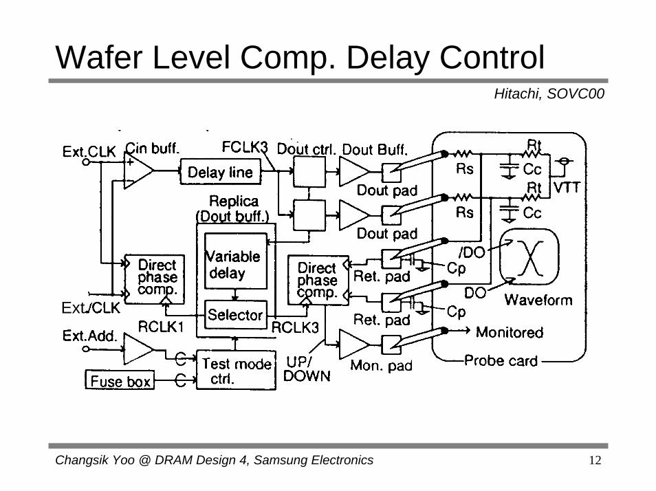
Wafer Level Comp. Delay ControlHitachi, SOVC00
Ext.

Changsik Yoo @ DRAM Design 4, Samsung Electronics 13
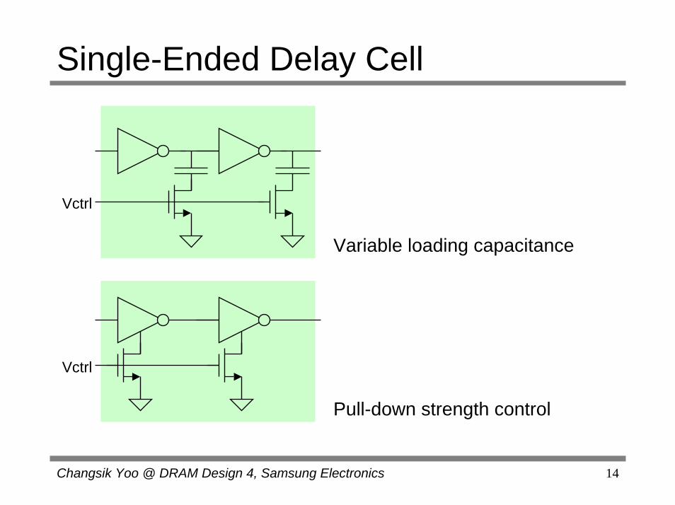
Delay Cell• Single-ended delay cell
– Simple– Dynamic power only (no static current)
• Differential delay cell– Complex biasing– Static power consumption– Immune to supply noise and thus smaller jitter
• Variables for delay control– Current– Capacitance– Resistance– Voltage swing
Changsik Yoo @ DRAM Design 4, Samsung Electronics 14
Single-Ended Delay Cell
Vctrl
Variable loading capacitance
Vctrl
Pull-down strength control

Changsik Yoo @ DRAM Design 4, Samsung Electronics 15
Differential Delay Cell
Vlow
Vctrl
• Replica biasing ensures constant voltage swing independent of control voltage.
Changsik Yoo @ DRAM Design 4, Samsung Electronics 16
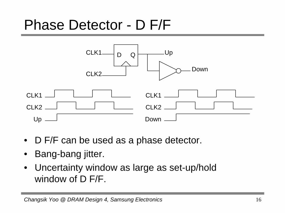
Phase Detector - D F/F
D QCLK1
CLK2
Up
Down
CLK1 CLK1
CLK2 CLK2
Up Down
• D F/F can be used as a phase detector.• Bang-bang jitter.• Uncertainty window as large as set-up/hold
window of D F/F.
Changsik Yoo @ DRAM Design 4, Samsung Electronics 17
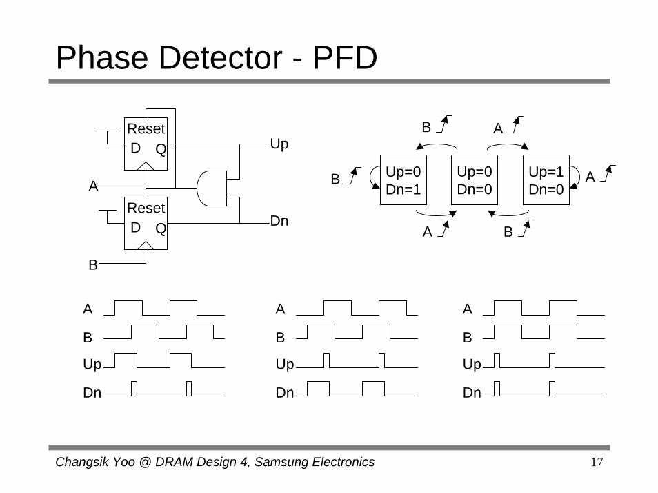
Phase Detector - PFD
Up=0Dn=1
Up=0Dn=0
Up=1Dn=0
A
A
A B
B
B
B
D QReset
D QReset
Up
Dn
A
A
B
Up
Dn
A
B
Up
Dn
A
B
Up
Dn
Changsik Yoo @ DRAM Design 4, Samsung Electronics 18
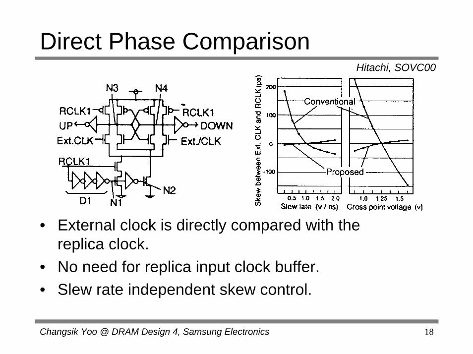
Direct Phase ComparisonHitachi, SOVC00
• External clock is directly compared with the replica clock.
• No need for replica input clock buffer.• Slew rate independent skew control.

Changsik Yoo @ DRAM Design 4, Samsung Electronics 19
Charge Pump• In analog DLL, PD output is converted to charge by
charge pump.• Charge pump output is low-pass filtered by a
capacitor.

Changsik Yoo @ DRAM Design 4, Samsung Electronics 20
Loop Filter• In conventional analog DLL, a capacitor is sufficient.• For fast standby-mode exit, locking information can
be stored in a digital code.– In digitally controlled DLL, a digital low-pass filter is
necessary.– Feedback delay should be considered when designing the
digital low-pass filter.
Changsik Yoo @ DRAM Design 4, Samsung Electronics 21
Agenda• Introduction• Building blocks of DLL• Design issues of DLL• DLL examples• Design examples
– DLL for DDR SDRAM – DLL for direct RDRAM
• Summary

Changsik Yoo @ DRAM Design 4, Samsung Electronics 22
Delay Range Problem of DLL - 1tD = delay from Ref-CLK to DLL-CLKtCC = clock periodtVCDL_max = max. delay of VCDLtVCDL_min = min. delay of VCDL
• DLL cannot distinguish between tD=∆ & tD=tCC+∆.

Changsik Yoo @ DRAM Design 4, Samsung Electronics 23
Delay Range Problem of DLL - 2• To prevent stuck/harmonic-lock problem, the
following relationship should be ensured.0.5 x tCC < tVCDL_min < tCC, tCC < tVCDL_max < 1.5 x tCC
→ Max ( tVCDL_min, 2/3 x tVCDL_max ) < tCC < Min ( 2 x tVCDL_min, tVCDL_max)
→ Limited locking range.
Changsik Yoo @ DRAM Design 4, Samsung Electronics 24
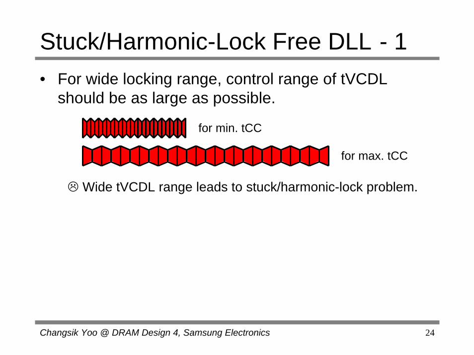
Stuck/Harmonic-Lock Free DLL - 1• For wide locking range, control range of tVCDL
should be as large as possible.
Wide tVCDL range leads to stuck/harmonic-lock problem.
for min. tCC
for max. tCC

Changsik Yoo @ DRAM Design 4, Samsung Electronics 25
Stuck/Harmonic-Lock Free DLL - 2• Initial locking starts with tVCDL_max or tVCDL_min.
– If locking starts from tVCDL_min or tVCDL_max, it is clear that tVCDL should be increased/decreased till DLL is locked.
• Use a PD which can prevent stuck/harmonic-lock problem.
• Develop a DLL which can find the stuck/harmonic-lock free initial condition.

Changsik Yoo @ DRAM Design 4, Samsung Electronics 26
Stuck/Harmonic-Lock Free PD
CLK1 - External ClockCLK2 - Internal ClockCLKM - Center-tap of VCDL
(a)
(b)
• With conventional PD, case (a) and (b) would give the same PD output, and thus stuck/harmonic-lock occurs.
SEC, ISSCC99

Changsik Yoo @ DRAM Design 4, Samsung Electronics 27
Stuck/Harmonic-Lock Free DLL - Ex.SNU, CICC99
• tRDC is settled at 1/8 x tCC by replica delay line.→ Stuck/harmonic-free locking range is greatly increased.
Changsik Yoo @ DRAM Design 4, Samsung Electronics 28
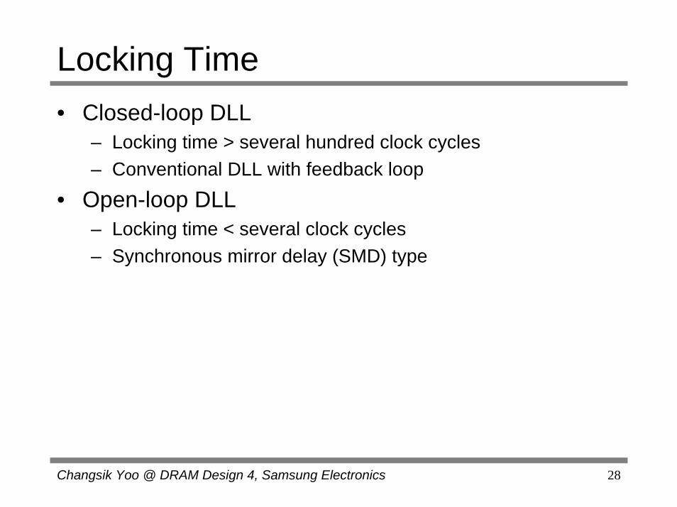
Locking Time• Closed-loop DLL
– Locking time > several hundred clock cycles– Conventional DLL with feedback loop
• Open-loop DLL– Locking time < several clock cycles– Synchronous mirror delay (SMD) type
Changsik Yoo @ DRAM Design 4, Samsung Electronics 29
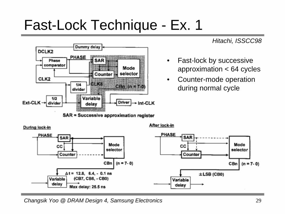
Fast-Lock Technique - Ex. 1Hitachi, ISSCC98
• Fast-lock by successive approximation < 64 cycles
• Counter-mode operation during normal cycle
Changsik Yoo @ DRAM Design 4, Samsung Electronics 30
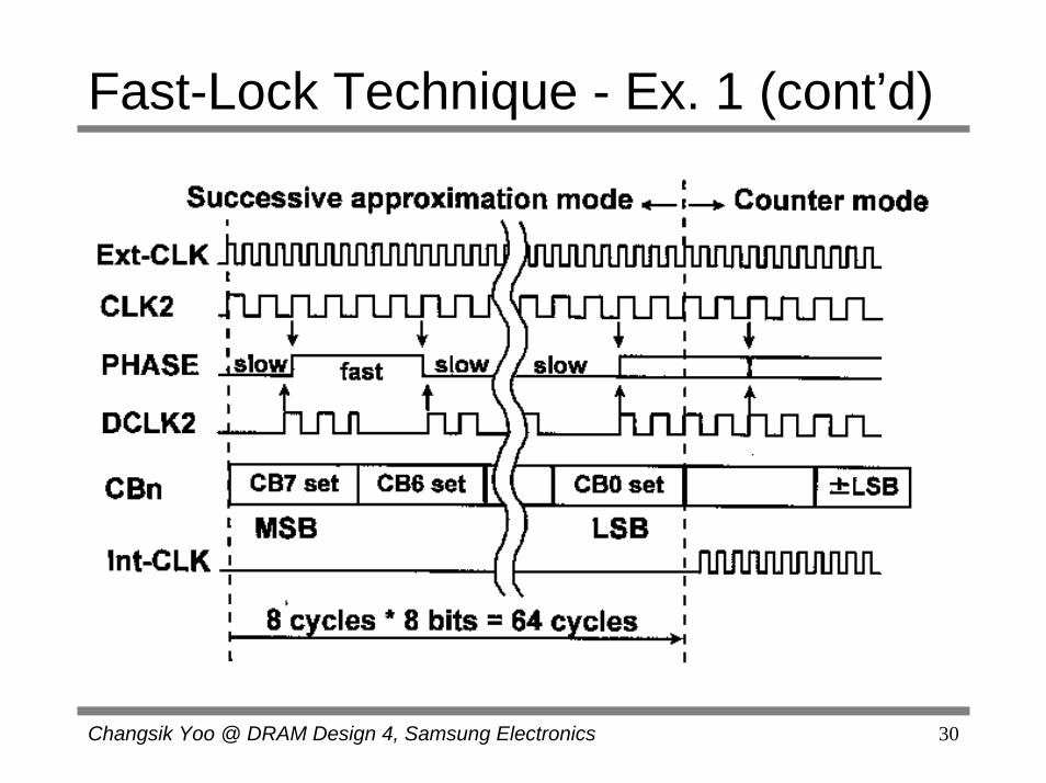
Fast-Lock Technique - Ex. 1 (cont’d)

Changsik Yoo @ DRAM Design 4, Samsung Electronics 31
Fast-Lock Technique - Ex. 2
Unit Delay
Meas. Delay Line
Compare & Latch
Voltage Controlled VDL
d2
d1
CP&LPFPD
Unit Delay
Dummy Delay(II)
Dummy Delay(I)Clock Buffer
Ext..CLK
InternalClock
Flag
DLL_EnableClock Driver
DLLBlock
d1 tCK
d1+d2
Vcont
d1
pclk
FB
updown
Patent Pending, SEC

Changsik Yoo @ DRAM Design 4, Samsung Electronics 32
DLL Locking Time for DDR SDRAM• In DDR SDRAM, DLL should be locked within 200
cycles after power-up sequence.– Not a hard job.– In DDR SDRAM, DLL is necessary only during read cycle.– For small standby current, it is desirable to turn off DLL
except read cycle which requires DLL to be able to provide stable clock within 4 cycles after turn-on.
– Initial locking right after power-up need not be faster than 200 cycles.
– Fast standby-mode exit is the key issue.
Changsik Yoo @ DRAM Design 4, Samsung Electronics 33
Agenda• Introduction• Building blocks of DLL• Design issues of DLL• DLL examples• Design examples
– DLL for DDR SDRAM – DLL for direct RDRAM
• Summary

Changsik Yoo @ DRAM Design 4, Samsung Electronics 34
Synchronous Mirror Delay (SMD) - 1NEC, ISSCC96
☺ Open-loop system ; fast locking < 2 cyclesArea penalty for wide freq. range and locking accuracy.
Meas. Delay LineExt. Clock
Compare & Transfer
Var. Delay LineInt. Clock
d1+d2tCC
d1
d2 tCC-(d1+d2)

Changsik Yoo @ DRAM Design 4, Samsung Electronics 35
Synchronous Mirror Delay (SMD) - 2
Ext. Clock
Input Buffer
Meas. Delay Line
Var. Delay Line
Int. Clock
d1 d1+d2 tCC -(d1+d2) (d1+d2)
tCC - d2
2*tCC - (d1+d2)

Changsik Yoo @ DRAM Design 4, Samsung Electronics 36
Hierarchical Phase-Locking Delay
FINE DELAY ELEM.(~0.2ns)
COARSE DELAY ELEM.(~1ns)
CLK BUFF.DELAY d1
CLK
PCLK_HPLDCLK DRIVER
DELAY d2
COARSE DELAY STAGE
FINE DELAY STAGE
DELAYELEMENT COMPARATOR
TDS
~ tCC - (d1 + d2)
~ tCC
CONVENTIONAL(DELAY ELEM. 0.2ns)
HIERARCHICAL(COARSE DELAY ELEM. : 1nsFINE DELAY ELEM. : 0.2ns)
Number of Delay Stage @ 50MHz (tCC=20ns)
20ns / 0.2ns = 100 (stage)
20ns / 1ns + 1ns / 0.2ns = 25 (stage)
TUNING
SWITCH
d1+d2
C1 C2 C3 C4 Cm-1 Cm
F1 F2 F3 F4 Fn-1 Fn
PCLK D1 D2 D3 D4
Dm
G1 G2 G3 G4 Gn
SEC, SOVC96
Changsik Yoo @ DRAM Design 4, Samsung Electronics 37
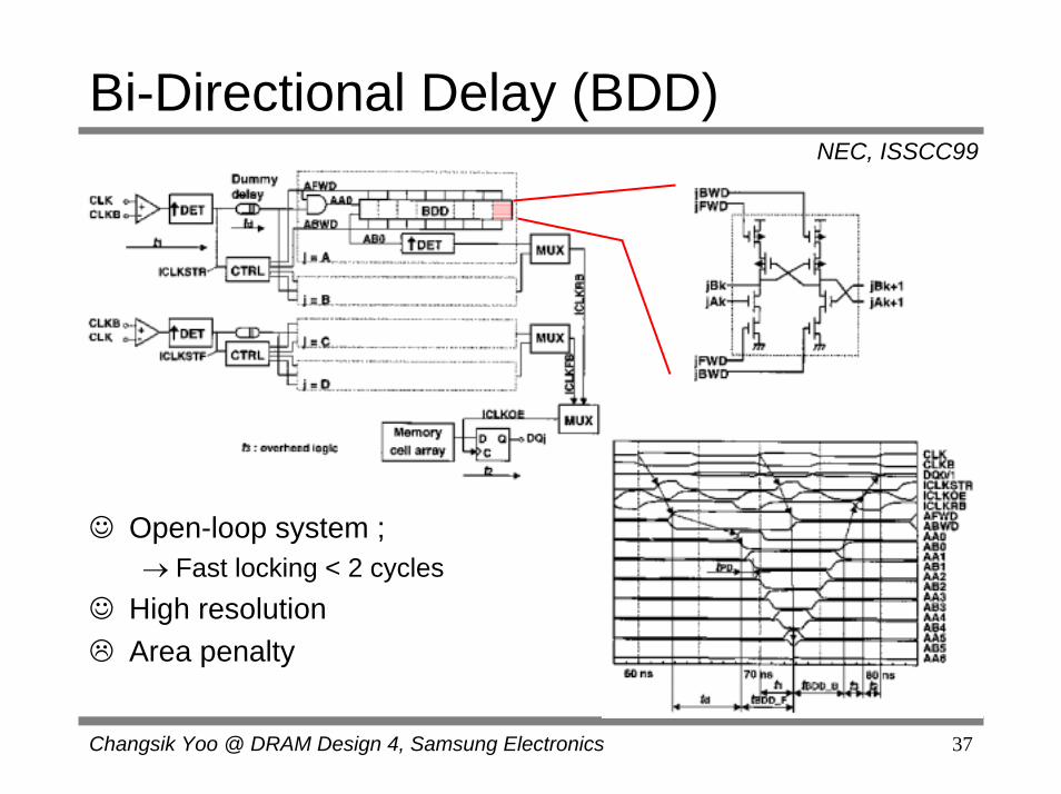
Bi-Directional Delay (BDD)NEC, ISSCC99
☺ Open-loop system ; → Fast locking < 2 cycles
☺ High resolutionArea penalty
Changsik Yoo @ DRAM Design 4, Samsung Electronics 38
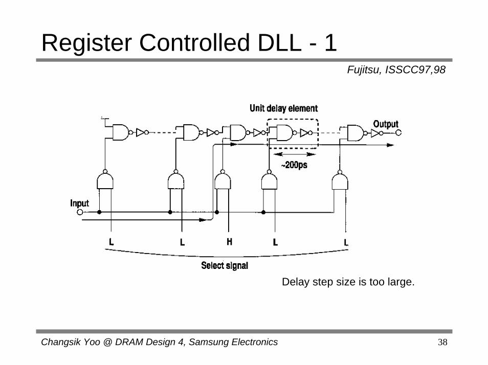
Register Controlled DLL - 1Fujitsu, ISSCC97,98
Delay step size is too large.

Changsik Yoo @ DRAM Design 4, Samsung Electronics 39
Register Controlled DLL - 2Fujitsu, ISSCC97,98
☺ Locking information is stored as a digital code. → Fast standby-mode exit
☺ High resolution thanks to vernier type delay line.
Changsik Yoo @ DRAM Design 4, Samsung Electronics 40
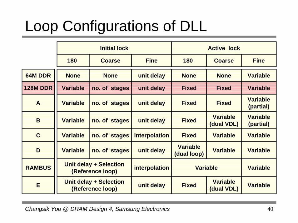
Loop Configurations of DLLInitial lock Active lock
180° Coarse Fine 180° Coarse Fine
64M DDR None None unit delay None None Variable
128M DDR Variable no. of stages unit delay Fixed Fixed Variable
Variable(partial)A Variable no. of stages unit delay Fixed Fixed
Variable(dual VDL)
Variable(partial)B Variable no. of stages unit delay Fixed
C Variable no. of stages interpolation Fixed Variable Variable
Unit delay + Selection(Reference loop) interpolation VariableRAMBUS
Variable(dual loop)D Variable no. of stages unit delay Variable Variable
Variable
Unit delay + Selection(Reference loop)
Variable(dual VDL)E unit delay Fixed Variable
Changsik Yoo @ DRAM Design 4, Samsung Electronics 41
Agenda• Introduction• Building blocks of DLL• Design issues of DLL• DLL examples• Design examples
– DLL for DDR SDRAM – DLL for direct RDRAM
• Summary
Changsik Yoo @ DRAM Design 4, Samsung Electronics 42
DLL for DDR SDRAM• Wide locking range
– tCC ; 6ns ~ 15ns• Jitter specification is not tough.
– tAC, tDQSCK ; +/-0.75ns– tDQSQ ; +/-0.5ns @ tCC = 7.5ns– But, most of the jitter comes from SSO noise of DOUT buffer
and thus the DLL jitter should be minimized.• Locking time < 200 cycles• Power consumption < 20mA
– As small as possible

Changsik Yoo @ DRAM Design 4, Samsung Electronics 43
Hybrid DLL for DDR SDRAM - 1SEC, ISSCC’99
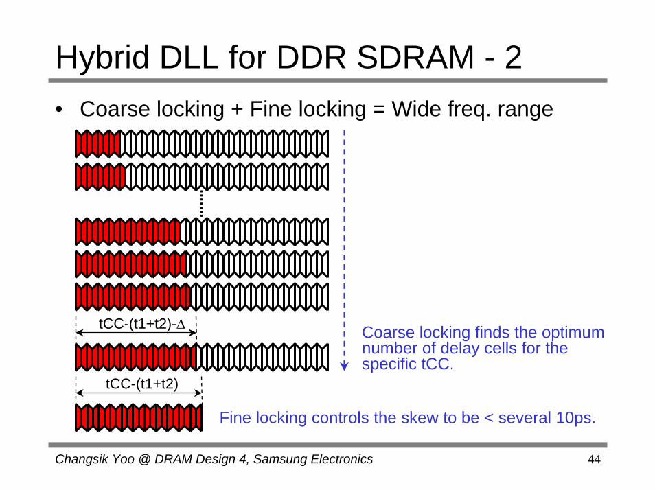
Changsik Yoo @ DRAM Design 4, Samsung Electronics 44
Hybrid DLL for DDR SDRAM - 2• Coarse locking + Fine locking = Wide freq. range
tCC-(t1+t2)-∆ Coarse locking finds the optimumnumber of delay cells for the specific tCC.
Fine locking controls the skew to be < several 10ps.
tCC-(t1+t2)

Changsik Yoo @ DRAM Design 4, Samsung Electronics 45
Hybrid DLL for DDR SDRAM - 3
Changsik Yoo @ DRAM Design 4, Samsung Electronics 46
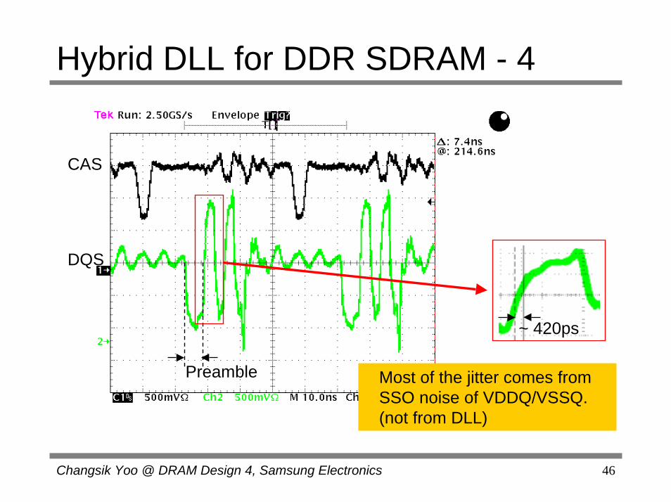
Hybrid DLL for DDR SDRAM - 4
CAS
DQS
Preamble Most of the jitter comes from SSO noise of VDDQ/VSSQ.(not from DLL)
~ 420ps
Changsik Yoo @ DRAM Design 4, Samsung Electronics 47
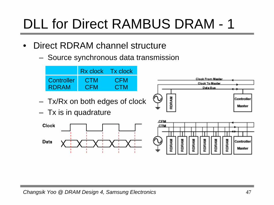
DLL for Direct RAMBUS DRAM - 1• Direct RDRAM channel structure
– Source synchronous data transmission
– Tx/Rx on both edges of clock– Tx is in quadrature
ControllerRx clock Tx clock
CTM CFMRDRAM CFM CTM
Changsik Yoo @ DRAM Design 4, Samsung Electronics 48
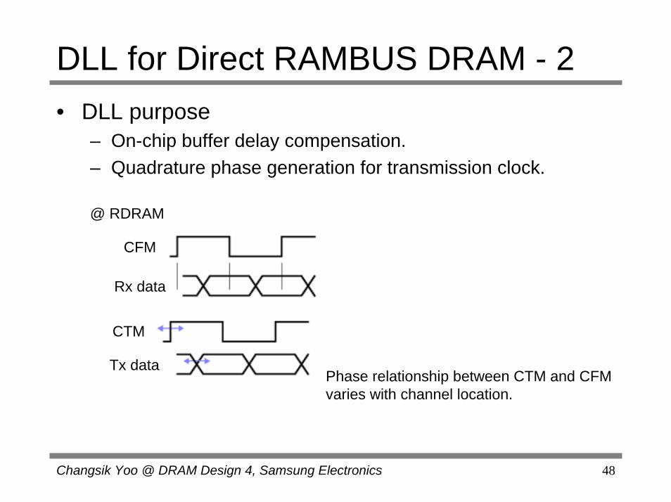
DLL for Direct RAMBUS DRAM - 2• DLL purpose
– On-chip buffer delay compensation.– Quadrature phase generation for transmission clock.
@ RDRAM
CFM
Rx data
CTM
Tx dataPhase relationship between CTM and CFM varies with channel location.
Changsik Yoo @ DRAM Design 4, Samsung Electronics 49
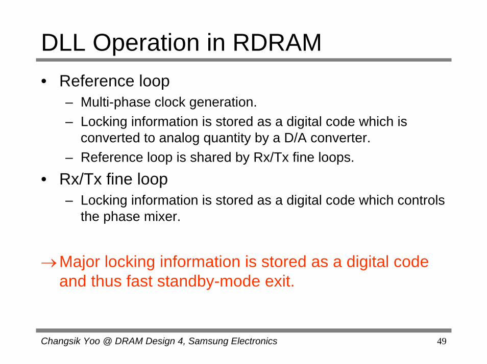
DLL Operation in RDRAM • Reference loop
– Multi-phase clock generation.– Locking information is stored as a digital code which is
converted to analog quantity by a D/A converter.– Reference loop is shared by Rx/Tx fine loops.
• Rx/Tx fine loop– Locking information is stored as a digital code which controls
the phase mixer.
→Major locking information is stored as a digital code and thus fast standby-mode exit.
Changsik Yoo @ DRAM Design 4, Samsung Electronics 50
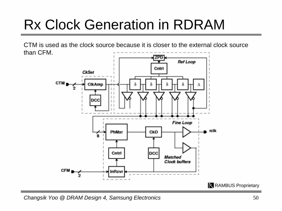
Rx Clock Generation in RDRAM
RAMBUS Proprietary
CTM is used as the clock source because it is closer to the external clock source than CFM.
Changsik Yoo @ DRAM Design 4, Samsung Electronics 51
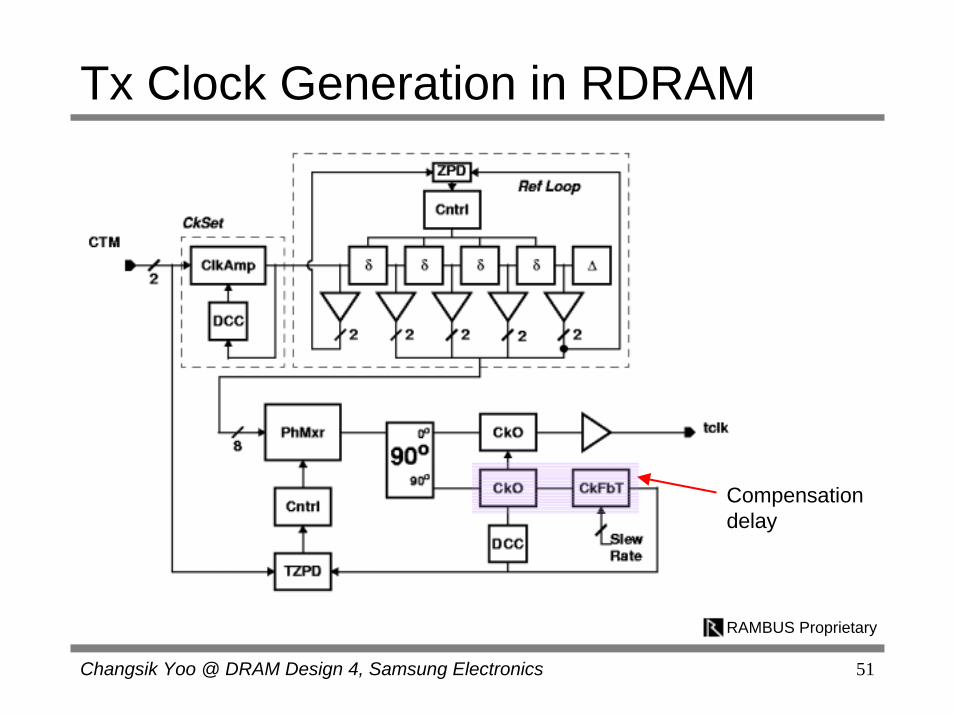
Tx Clock Generation in RDRAM
Compensationdelay
RAMBUS Proprietary

Changsik Yoo @ DRAM Design 4, Samsung Electronics 52
90o Phase Generation
RAMBUS Proprietary
Changsik Yoo @ DRAM Design 4, Samsung Electronics 53
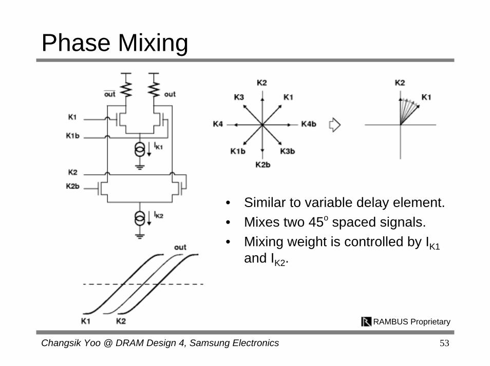
Phase Mixing
RAMBUS Proprietary
• Similar to variable delay element.• Mixes two 45o spaced signals.• Mixing weight is controlled by IK1
and IK2.

Changsik Yoo @ DRAM Design 4, Samsung Electronics 54
Duty Cycle Correction• For maximum valid data window• DCC information is stored in a loop capacitor.
• If tHigh = tLow, control voltage is stabilized.RAMBUS Proprietary

Changsik Yoo @ DRAM Design 4, Samsung Electronics 55
Agenda• Introduction• Building blocks of DLL• Design issues of DLL• DLL examples• Design examples
– DLL for DDR SDRAM – DLL for direct RDRAM
• Summary
Changsik Yoo @ DRAM Design 4, Samsung Electronics 56
Summary• DLL should be designed considering the
system requirement.– Locking time– Power consumption– Standby-mode exit– Area