
Chapter 7 MOSFETs in ICs – Scaling, Leakage, and Other...
44
Modern Semiconductor Devices for Integrated Circuits (C. Hu) Slide 7-1 Chapter 7 MOSFETs in ICs – Scaling, Leakage, and Other Topics 7.1 Technology Scaling - for Cost, Speed, and Power Consumption •New technology node every two years or so. Defined by minimum line width-spacing average. • Feature sizes are ~70% of previous node’s. • Reduction of circuit area by 2 ― good for cost and speed. YEAR 1992 1995 1997 1999 2001 2003 2005 2007 Technology Generation 0.5 μm 0.35 μm 0.25 μm 0.18 μm 0.13 μm 90 nm 65 nm 45 nm
Transcript of Chapter 7 MOSFETs in ICs – Scaling, Leakage, and Other...

Modern Semiconductor Devices for Integrated Circuits (C. Hu) Slide 7-1
Chapter 7 MOSFETs in ICs – Scaling, Leakage, and Other Topics
7.1 Technology Scaling - for Cost, Speed, and Power Consumption
•New technology node every two years or so. Defined by minimum line width-spacing average.• Feature sizes are ~70% of previous node’s.• Reduction of circuit area by 2 ― good for cost and speed.
YEAR 1992 1995 1997 1999 2001 2003 2005 2007
Technology Generation
0.5µm
0.35µm
0.25µm
0.18µm
0.13µm
90nm
65nm
45nm

Modern Semiconductor Devices for Integrated Circuits (C. Hu) Slide 7-2
International Technology Roadmap for Semiconductors
• Vdd is reduced at each node to contain power consumption in spite of rising transistor density and frequency• Tox is reduced to raise Ion and retain good transistor behaviors• HP: High performance; LSTP: Low stand-by power
Year of Shipment 2003 2005 2007 2010 2013Technology Node (nm) 90 65 45 32 22Lg (nm) (HP/LSTP) 37/65 26/45 22/37 16/25 13/20
EOTe(nm) (HP/LSTP) 1.9/2.8 1.8/2.5 1.2/1.9 0.9/1.6 0.9/1.4
VDD (HP/LSTP) 1.2/1.2 1.1/1.1 1.0/1.1 1.0/1.0 0.9/0.9
Ion,HP (µA/µm) 1100 1210 1500 1820 2200
Ioff,HP (µA/µm) 0.15 0.34 0.61 0.84 0.37
Ion,LSTP (µA/µm) 440 465 540 540 540
Ioff,LSTP (µA/µm) 1e-5 1e-5 3e-5 3e-5 2e-5Strained Silicon High-k/Metal-Gate
Wet LithographyNew Structure

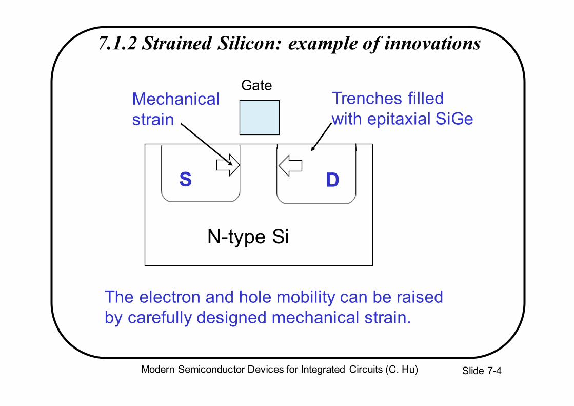
Modern Semiconductor Devices for Integrated Circuits (C. Hu) Slide 7-4
7.1.2 Strained Silicon: example of innovations
The electron and hole mobility can be raised by carefully designed mechanical strain.
N-type Si
Trenches filled with epitaxial SiGe
Gate
S D
Mechanical strain

Modern Semiconductor Devices for Integrated Circuits (C. Hu) Slide 7-5
7.2 Subthreshold Current• The leakage current that flows at Vg<Vt is called the
subthreshold current.
90nm technology. Gate length: 45nm
• The current at Vgs=0 and Vds=Vdd is called Ioff.
Intel, T. Ghani et al., IEDM 2003
I ds
( µA
/µm
)
Vgs
VtVt

Modern Semiconductor Devices for Integrated Circuits (C. Hu) Slide 7-6
ηϕ 1
=+
=depoxe
oxe
g
s
CCC
dVd
CdepψS
Cox
Vg
• Subthreshold current µns (surface inversion carrier concentration)
• nsµeqjs/kT
• js varies with Vg through a capacitor network
In subthreshold, js = constant +Vg/η
ϕS
EfEf, Ec
Vgs

Modern Semiconductor Devices for Integrated Circuits (C. Hu) Slide 7-7
Subthreshold Leakage Current( ) / kTVqkTq
sgss eendsI
ηϕ /constant/ kTqVgseη/µµµµ +
Cdepjs
Cox
VG
dep
oxeC
Cη = 1 +
• Subthreshold current changes 10x for η·60mV change in Vg. Reminder: 60mV is (ln10)·kT/q
•Subthreshold swing, S : the change in Vgs corresponding to 10x change in subthreshold current. S = η·60mV, typically 80-100mV
kTqVgseη/µdsI

Modern Semiconductor Devices for Integrated Circuits (C. Hu) Slide 7-8
Subthreshold Leakage Current
is determined only by Vt and subthreshold swing.
• Practical definition of Vt : the Vgs at which Ids= 100nA×W/L
=> ( ) kTVVq tgeL
WsubthresholdI /100
− ( ) SVV tg
LW /10100 −××=××nA)( » η
Vgs
Log (Ids )
Vt
100×W/L(nA)Vds=Vdd
Ioff
W SVtL
/10100 −××Ioff (nA) =
1/S

Modern Semiconductor Devices for Integrated Circuits (C. Hu) Slide 7-9
Subthreshold Swing
• Smaller S is desirable (lower Ioff for a given Vt). Minimum possible value of S is 60mV/dec.
• How do we reduce swing?• Thinner Tox => larger Coxe• Lower substrate doping => smaller Cdep• Lower temperature
• Limitations• Thinner Tox ― oxide breakdown reliability or oxide leakage
current • Lower substrate doping ― doping is not a free parameter but
set by Vt.
⎟⎟⎠
⎞⎜⎜⎝
⎛+⋅=
oxe
dep
CC
mVS 160

Modern Semiconductor Devices for Integrated Circuits (C. Hu) Slide 7-10
Effect of Interface States on Subthreshold Swing
⎟⎟⎠
⎞⎜⎜⎝
⎛ ++⋅=
oxe
sdep
CddQC
mVSφ/
160 int
Vg1
Vg2>Vg1
• Interface states may be filled by electrons or empty depending on its energy relative to EF, i.e., depending on Vg.
• dQint/d (number or interface state per eV-cm2) presents another capacitance in parallel with Cdep
sϕ

Modern Semiconductor Devices for Integrated Circuits (C. Hu) Slide 7-11
7.3 Vt Roll-off
65nm technology. EOT=1.2nm, Vdd=1VK. Goto et al., (Fujitsu) IEDM 2003
• Vt roll-off: Vt decreases with decreasing Lg.
• It determines the minimum acceptable Lgbecause Ioff is too large if Vt becomes too small.
• Question: Why data is plotted against Lg, not L?Answer: L is difficult to measure. Lg is. Also, Lg is the quantity that manufacturing engineers can control directly.
0.01 0.1 1-0.25
-0.20
-0.15
-0.10
-0.05
0.00
Vds = 50mV Vds = 1.0V
Symbols: TCADLines: Model
Vt R
oll-o
ff (V
)Lg (um)

Modern Semiconductor Devices for Integrated Circuits (C. Hu) Slide 7-12
Why Does Vt Decrease with L?― Potential Barrier Concept
• When L is small, smaller Vg is needed to reduce the barrier to 0.2V, i.e. Vt is smaller.
• Vt roll-off is greater for shorter L
~0.2V
Vds
Ec
Vgs=0V
Vgs=Vt-long
Long Channel
N+ Source
N+ Drain
Vg=0V
Vg=Vt

Modern Semiconductor Devices for Integrated Circuits (C. Hu) Slide 7-13
• Vds dependence
Energy-Band Diagram from Source to Drain
• L dependence
long channel
Vds
short channel
source/channel barrier
Vgs
log(Ids)
Vds
long channel
short channel
Vds=0
Vds=Vdd Vds=Vdd
Vds=0

Modern Semiconductor Devices for Integrated Circuits (C. Hu) Slide 7-14
Vt Roll-off – Simple Capacitance Model
As the channel length is reduced, drain to channel distance is reducedà Cdincreases
oxe
ddslongtt C
CVVV ⋅−= −
Vds helps Vgs to invert the surface, therefore
Due to built-in potential between N-
channel and N+ drain & source
( )oxe
ddslongtt C
CVVV ⋅+−= − 4.0
( )3
l/
where
4.0
jdepoxd
Ldslongtt
XWTl
eVVV d
≈
⋅+−= −−
• 2-D Poisson Eq. solution shows that Cd is an exponential function of L.
Cdn+ Xj
P-Sub
Coxe
Wdep
Tox
Vgs
Vds

Modern Semiconductor Devices for Integrated Circuits (C. Hu) Slide 7-15
( )3
l/
where
4.0
jdepoxd
Ldslongtt
XWTl
eVVV d
≈
⋅+−= −−
• Vertical dimensions (Tox, Wdep, Xj) must be scaled to support L reduction
Modern Semiconductor Devices for Integrated Circuits (C. Hu) Slide 7-16
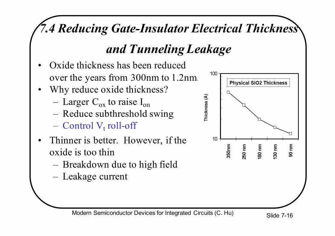
7.4 Reducing Gate-Insulator Electrical Thickness and Tunneling Leakage
• Oxide thickness has been reduced over the years from 300nm to 1.2nm.
• Why reduce oxide thickness?– Larger Cox to raise Ion– Reduce subthreshold swing– Control Vt roll-off
• Thinner is better. However, if the oxide is too thin– Breakdown due to high field– Leakage current

Modern Semiconductor Devices for Integrated Circuits (C. Hu) Slide 7-17
Gate Tunneling Leakage Current
• For SiO2 films thinner than 1.5nm, tunneling leakage current has become the limiting factor.
• HfO2 has several orders lower leakage for the same EOT.

Modern Semiconductor Devices for Integrated Circuits (C. Hu) Slide 7-18
Replacing SiO2 with HfO2---High-k Dielectric
• HfO2 has a relative dielectric constant (k) of ~24, six times large than that of SiO2.
• For the same EOT, the HfO2 film presents a much thicker (albeit a lower) tunneling barrier to the electrons and holes.
• Toxe can be further reduced by introducing metal-gate technology since the poly-depletion effect is eliminated.
(After W. Tsai et al., IEDM’03)

Modern Semiconductor Devices for Integrated Circuits (C. Hu) Slide 7-19
Challenges of High-K Technology• The difficulties of high-k dielectrics:
– chemical reactions between them and the silicon substrate and gate,
– lower surface mobility than the Si/SiO2 system– too low a Vt for P-channel MOSFET (as if there is
positive charge in the high-k dielectric).– long-term reliability
• A thin SiO2 interfacial layer may be inserted between Si-substrate and high-k film.
Question: How can Tinv be reduced?(Answer is in Sec. 7.4 text)

Modern Semiconductor Devices for Integrated Circuits (C. Hu) Slide 7-20
7.5 How to Reduce Wdep
depox
stsstfb
ox
stssubstfbt WC
VC
qNVV φε
φφε
φ22
++=++=
• Or use retrograde doping with very thin lightly doped surface layer– Also, less impurity
scattering in the inversion layer à higher mobility
• Wdep can be reduced by increasing Nsub
– If Nsub is increased, Cox has to be increased in order to keep Vt the same.
– Wdep can be reduced in proportion to Tox.

Modern Semiconductor Devices for Integrated Circuits (C. Hu) Slide 7-21
7.5 Ideal Retrograde Doping Profile
)21(depox
oxsstfbt W
TVVεε
φ ++=
• Compared with uniformly doped body
• Assume the body is heavily doped with an undoped layer, Trg thick, at the surface.
•Ideal retrograde doping yields a depletion region width (Trg) half as thick as Wdep of a uniform doped body.

Modern Semiconductor Devices for Integrated Circuits (C. Hu) Slide 7-22
7.6 Shallow Junction and Metal Source/Drain
• The shallow junction extension helps to control Vt roll-off.• Shallow junction and light doping combine to produce an
undesirable parasitic resistance that reduces the precious Ion.
• Theoretically, metal S/D can be used as a very shallow “junction”.
shallow junctionextension
This image cannot
gateoxide
dielectric spacercontact metal
channel
Deep S/Dsilicide

Modern Semiconductor Devices for Integrated Circuits (C. Hu) Slide 7-23
7.6.1 MOSFET with Metal Source/Drain
To unleash the potentials of Schottky S/D MOSFET, a low- Schottky junction is needed for NFETs and low- for PFET.
Bnφ
Bpφ

Modern Semiconductor Devices for Integrated Circuits (C. Hu) Slide 7-24
7.7 Variations and Design for Manufacturing
• Higher Ion goes hand-in-hand with larger Ioff -- think L, Vt, Tox, Vdd.
• Figure shows spread in Ion (and Ioff) produced by intentional difference in Lg and unintentional manufacturing variatons in Lg and other parameters.
NMOS PMOS
Intel, T. Ghani et al., IEDM 2003

Modern Semiconductor Devices for Integrated Circuits (C. Hu) Slide 7-25
Variation Tolerant Circuit Design• Multiple Vt
– Lower Vt is used only in the blocks that need speed• Multiple Vdd
– Higher Vdd is used only in the blocks that need speed• Substrate (well) bias
– Only some circuit blocks need to operate at high speed.– Can use reverse well bias to raise the Vt for the rest.– This techniques can also reduce the chip-to-chip and
block-to-block variations with intelligent control circuitry.
– Would like larger body effect than conventional MOSFET.

Modern Semiconductor Devices for Integrated Circuits (C. Hu) Slide 7-26
7.8 Ultra-Thin-Body SOI and Multigate MOSFETs
• Reducing Tox gives the gate excellent control of Si surface potential.
• But, the drain could still have more control than the gate along sub-surface leakage current paths. (Right figure.)
CdCg
leakage path
DSCd
S
P-Sub
CgTox
Vgs
Vds
D
Vgs
Vds
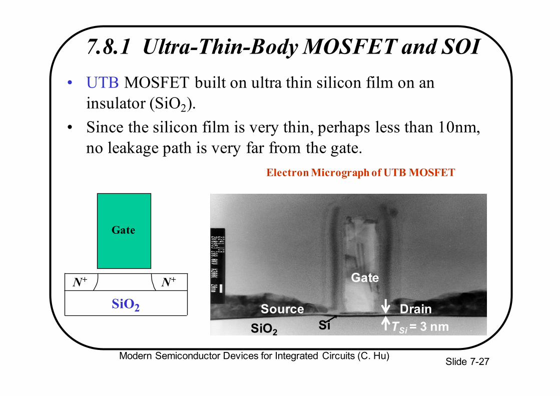
Modern Semiconductor Devices for Integrated Circuits (C. Hu) Slide 7-27
7.8.1 Ultra-Thin-Body MOSFET and SOI• UTB MOSFET built on ultra thin silicon film on an
insulator (SiO2).• Since the silicon film is very thin, perhaps less than 10nm,
no leakage path is very far from the gate.
Source DrainTSi = 3 nm
Gate
SiO2 Si
Electron Micrograph of UTB MOSFET
Gate
N+ N+
SiO2

Modern Semiconductor Devices for Integrated Circuits (C. Hu) Slide 7-28
Ultra-Thin-Body MOSFET• The subthreshold leakage is reduced as the silicon
film is made thinner.
Tox=1.5nm, Nsub=1e15cm-3, Vdd=1V, Vgs=0
Modern Semiconductor Devices for Integrated Circuits (C. Hu) Slide 7-29
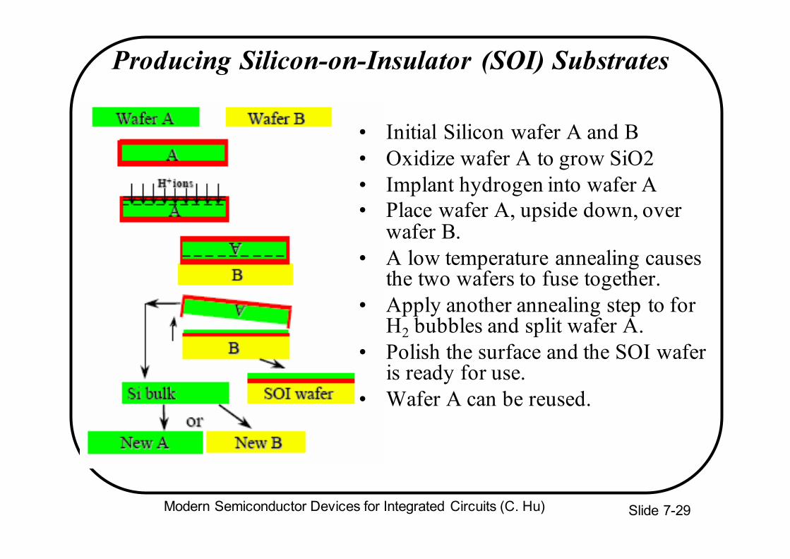
Producing Silicon-on-Insulator (SOI) Substrates
• Initial Silicon wafer A and B• Oxidize wafer A to grow SiO2• Implant hydrogen into wafer A• Place wafer A, upside down, over
wafer B. • A low temperature annealing causes
the two wafers to fuse together.• Apply another annealing step to for
H2 bubbles and split wafer A.• Polish the surface and the SOI wafer
is ready for use. • Wafer A can be reused.

Modern Semiconductor Devices for Integrated Circuits (C. Hu) Slide 7-30
Cross-Section of SOI Circuits
• Due to the high cost of SOI wafers, only some microprocessors, which command high prices and compete on speed, have embraced this technology.
• In order to benefit from the UTB concept, Si film thickness must be agreesively reduced to ~ Lg/4
SiBuried Oxide
Si substrate

Modern Semiconductor Devices for Integrated Circuits (C. Hu) Slide 7-31
7.8.2 Multi-gate MOSFET and FinFET• The second way of eliminating deep leakage paths is to
provide gate control from more than one side of the channel.• The Si film is very thin so that no leakage path is far from one
of the gates. • Because there are more than one gates, the structure may be
called multi-gate MOSFET.
Source Drain
Gate 1 Vg
Tox
TSiSi
Gate 2double-gate MOSFET

Modern Semiconductor Devices for Integrated Circuits (C. Hu) Slide 7-32
FinFET• One multi-gate structure, called FinFET,
is particularly attractive for its simplicity of fabrication.
• The channel consists of the two vertical surfaces and the top surface of the fin.
• Question: What is the channel width, W?Answer: The sum of twice the fin height and the
width of the fin.Gate
Si
BOX
Gate
Si
BOX STI
Gate
SiSTISTI
Gate
SiSTI
SOI FinFET Bulk FinFET

Modern Semiconductor Devices for Integrated Circuits (C. Hu) Slide 7-33
Variations of FinFET
Nanowire FinFET
Short FinFET
Tall FinFET
• Tall FinFET has the advantage of providing a large W and therefore large Ion while occupying a small footprint.
• Short FinFET has the advantage of less challenging lithography and etching.
• Nanowire FinFET gives the gate even more control over the silicon wire by surrounding it.
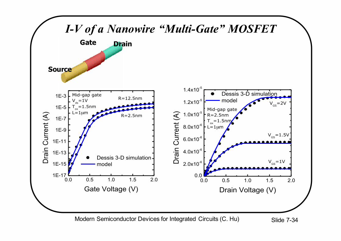
Modern Semiconductor Devices for Integrated Circuits (C. Hu) Slide 7-34
0.0 0.5 1.0 1.5 2.00.0
2.0x10⁻⁶
4.0x10⁻⁶
6.0x10⁻⁶
8.0x10⁻⁶
1.0x10⁻⁵
1.2x10⁻⁵
1.4x10⁻⁵
VGS
=1V
VGS
=1.5V
VGS
=2VMid-gap gateR=2.5nmT
ox=1.5nm
L=1µm
Drai
n Cu
rrent
(A)
Drain Voltage (V)
Dessis 3-D simulation model
Source
Gate Drain
I-V of a Nanowire “Multi-Gate” MOSFET
0.0 0.5 1.0 1.5 2.01E-17
1E-15
1E-13
1E-11
1E-9
1E-7
1E-5
1E-3 R=12.5nm
R=2.5nm
Mid-gap gateV
ds=1V
Tox
=1.5nmL=1µm
Drai
n Cu
rrent
(A)
Gate Voltage (V)
Dessis 3-D simulation model

Modern Semiconductor Devices for Integrated Circuits (C. Hu) Slide 7-35
What Parameters Determine the gds ?
ds
t
t
atds
ds
atdsds dV
dVdVdI
dVdI
g ⋅=≡
msatgs
atds
t
atds gdVdI
dVdI
−=−
=
dlLmsatds egg /−×=
•A larger L or smaller ld , i.e. smaller Tox, Wdep, Xj, can increase the maximum voltage gain.•The cause is “Vt dependence on Vds”in short channel transistors.
dlL
ds
msat egg /)(R gain voltageMax ==∞→
and
Idsat is a function of Vgs-Vt(From Eq. 7.3.3, )dlLedsVlongtVtV
/⋅−−=
dlL
ds
T edVdV /−=
7.9 Output Conductance

Modern Semiconductor Devices for Integrated Circuits (C. Hu) Slide 7-36
Channel Length Modulation
( )dsatds
atdsdds VVL
Ilg
−
⋅=
3jdepoxd XWTl ≈
• For large L and Vds close to Vdsat, another mechanism may dominate gds. That is channel length modulation.•Vds-Vdsat, is dissipated over a short distance next to drain, causing the “channel length” to decrease. More with increasing Vds.
ΔL
Vd>Vdsat
Vc=Vdsat

Modern Semiconductor Devices for Integrated Circuits (C. Hu) Slide 7-37
7.10 Device and Process Simulation• Device Simulation
– Commercially available computer simulation tools can solve all the equations presented in this book simultaneously with few or no approximations.
– Device simulation provides quick feedback about device design before long and expensive fabrication.
• Process Simulation– Inputs to process simulation: lithography mask pattern,
implantation dose and energy, temperatures and times for oxidization and annealing steps, etc.
– The process simulator generates a 2-D or 3-D structures with all the deposited or grown and etched thin films and doped regions.
– This output may be fed into a device simulator as input together with applied voltages.
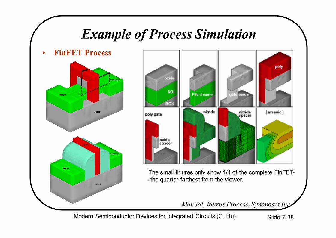
Modern Semiconductor Devices for Integrated Circuits (C. Hu) Slide 7-38
Example of Process Simulation• FinFET Process
Manual, Taurus Process, Synoposys Inc.
The small figures only show 1/4 of the complete FinFET--the quarter farthest from the viewer.

Modern Semiconductor Devices for Integrated Circuits (C. Hu) Slide 7-39
Example of Device Simulation---Density of Inversion Charge in the Cross-Section of a FinFET Body
• The inversion layer has a significant thickness (Tch).• There are more more subthreshold inversion electrons at
the corners.
S
D
G
Tall FinFET Short FinFETC.-H. Lin et al., 2005 SRC TECHCON
Modern Semiconductor Devices for Integrated Circuits (C. Hu) Slide 7-40
7.11 MOSFET Compact Modeling for Circuit Simulation
• For circuit simulation, MOSFETs are modeled with analytical equations.
• Device model is the link between technology/manufacturing and design/product. The other link is design rules.
• Circuits are designed A. through circuit simulations or B. using cell libraries that have been carefully designed beforehand using circuit simulations.
• BSIM is the first industry standard MOSFET model. It contains all the models presented in these chapters and more.

Modern Semiconductor Devices for Integrated Circuits (C. Hu) Slide 7-41
Examples of BSIM Model Results

Modern Semiconductor Devices for Integrated Circuits (C. Hu) Slide 7-42
Example of BSIM Model Results

Modern Semiconductor Devices for Integrated Circuits (C. Hu) Slide 7-43
Example of BSIM Model Results

Modern Semiconductor Devices for Integrated Circuits (C. Hu) Slide 7-44
7.12 Chapter SummaryThe major component of Ioff is the subthreshold current
SVkTqVoff
tt
LWe
LWnAI // 10100 100)( −− ⋅⋅=⋅⋅= η
( ) dLdslongtt eVVV l/4.0 −
− ⋅+−=3
jdepoxed XWT∝l
Vt decreases with L, a fact known as Vt roll-off, caused by drain-induced barrier lowering (DIBL).
Output conductance of short channel transistors
dlLmsatds egg /−×=


![[03] Chapter02_Logic Design With MOSFETs](https://static.fdocuments.us/doc/165x107/577cd29c1a28ab9e7895a726/03-chapter02logic-design-with-mosfets.jpg)


![[06] Chapter06_Electrical Characteristic of MOSFETs](https://static.fdocuments.us/doc/165x107/55cf968e550346d0338c45ba/06-chapter06electrical-characteristic-of-mosfets.jpg)
