CHAPTER 7 – HIGH PERFORMANCE CMOS OP AMPS7-4-06)… · · 2008-10-06Chapter 7 – Introduction...
74
Chapter 7 – Introduction (7/4/06)) Page 7.0-1. CMOS Analog Circuit Design © P.E. Allen - 2006 CHAPTER 7 – HIGH PERFORMANCE CMOS OP AMPS INTRODUCTION Chapter Outline 7.1 Buffered Op Amps 7.2 High-Speed/Frequency Op Amps 7.3 Differential Output Op Amps 7.4 Micropower Op Amp 7.5 Low-Noise Op Amps 7.6 Low Voltage Op Amps Goal To illustrate the degrees of freedom and choices of different circuit architectures that can enhance the performance of a given op amp. 060703-01 Simple Op Amp Buffered High Frequency Differential Output Low Power Low Noise Low Voltage Chapter 7 – Section 1 (7/4/06)) Page 7.1-1. CMOS Analog Circuit Design © P.E. Allen - 2006 SECTION 7.1 – BUFFERED OP AMPS Objective The objective of this presentation is: 1.) Illustrate the method of lowering the output resistance of simple op amps 2.) Show examples Outline • Open-loop MOSFET buffered op amps • Closed-loop MOSFET buffered op amps (shunt negative feedback) • BJT output op amps • Summary
Transcript of CHAPTER 7 – HIGH PERFORMANCE CMOS OP AMPS7-4-06)… · · 2008-10-06Chapter 7 – Introduction...

Chapter 7 – Introduction (7/4/06)) Page 7.0-1.
CMOS Analog Circuit Design © P.E. Allen - 2006
CHAPTER 7 – HIGH PERFORMANCE CMOS OP AMPS INTRODUCTION
Chapter Outline
7.1 Buffered Op Amps 7.2 High-Speed/Frequency Op Amps 7.3 Differential Output Op Amps 7.4 Micropower Op Amp 7.5 Low-Noise Op Amps 7.6 Low Voltage Op Amps
Goal
To illustrate the degrees of freedom and choices of different circuit architectures that can enhance the performance of a given op amp.
060703-01
SimpleOp Amp
BufferedHigh FrequencyDifferential
Output
Low Power Low NoiseLow Voltage
Chapter 7 – Section 1 (7/4/06)) Page 7.1-1.
CMOS Analog Circuit Design © P.E. Allen - 2006
SECTION 7.1 – BUFFERED OP AMPS Objective
The objective of this presentation is:
1.) Illustrate the method of lowering the output resistance of simple op amps
2.) Show examples
Outline
• Open-loop MOSFET buffered op amps
• Closed-loop MOSFET buffered op amps (shunt negative feedback)
• BJT output op amps
• Summary
Chapter 7 – Section 1 (7/4/06)) Page 7.1-2.
CMOS Analog Circuit Design © P.E. Allen - 2006
What is a Buffered Op Amp?
A buffered op amp is an op amp with a low value of output resistance, Ro.
Typically, 10 Ro 1000
The result is a voltage-controlled, voltage-source amplifier.
Requirements
Generally the same as for the output amplifier:
• Low output resistance
• Large output signal swing
• Low distortion
• High efficiency
Chapter 7 – Section 1 (7/4/06)) Page 7.1-3.
CMOS Analog Circuit Design © P.E. Allen - 2006
The Source Follower as a Buffer
Class-A Follower:
• Simple, gain < 1 • Lower efficiency
• Rout = 1
gm + gmbs 500 to 1000
• Level shift from input to output
Push-Pull Follower:
• Voltage loss from 2 cascaded followers • Higher efficiency • Current in M1 and M2 determined by: VGS4 + VSG3 = VGS1 + VSG2
2I6
Kn'(W4/L4) + 2I5
Kp'(W3/L3)
= 2I1
Kn'(W1/L1) + 2I2
Kp'(W2/L2)
Use the W/L ratios to define I1 and I2 from I5 and I6 060706-02
VNBias1
VDD
M1
M2
vIN vOUT
VDD
VDD
M4VDD
VPBias1
VDD
M5
M3
M6
+−
VSG3
I5
I6
+−
VSG2+−
VGS4
+−
VGS1
I1
I2
060118-10
VNBias1
VDD
M1
M2
vIN
vOUT

Chapter 7 – Section 1 (7/4/06)) Page 7.1-4.
CMOS Analog Circuit Design © P.E. Allen - 2006
Two-Stage Op Amp with Follower
-
+vin
M1 M2
M3 M4
M5
M6
M7VNBias
Cc
CL
I5I7
060706-03
VDD
M8
M9
vout
I9
Power dissipation now becomes (I5 + I7 + I9)VDD
Gain becomes,
Av = gm1
gds2+gds4 gm6
gds6+gds7 gm8
gm8+ gmbs8+gds8+gds9
Chapter 7 – Section 1 (7/4/06)) Page 7.1-5.
CMOS Analog Circuit Design © P.E. Allen - 2006
Source-Follower, Push-Pull Output Op Amp
vout
VDD
VDD
Cc
-
+vin
M1 M2
M3
VSS
R1
M5
M6
R1
M7
M8
R1
M13
M14
VSS
VDD
VSS
M22
M21
IBias
M9
M10
M11
M12
M4
M17
M18
M15
M16
M19
M20
Fig. 7.1-1
CL
Buffer
-+VSG18
-+VSG21
-
+VGS19
-
+VGS22
I17
I20
Rout 1
gm21+gm22 1000 , Av(0)=65dB (IBias=50μA), and GB = 60MHz for CL = 1pF

Chapter 7 – Section 1 (7/4/06)) Page 7.1-6.
CMOS Analog Circuit Design © P.E. Allen - 2006
Compensation of Op Amps with Output Amplifiers Compensation of a three-stage amplifier: This op amp introduces a third pole, p’3 (what about zeros?) With no compensation,
Vout(s)Vin(s) =
-Avos
p’1 - 1s
p’2 - 1s
p’3 - 1
Illustration of compensation choices:
p1'p2'p3' p1
p2
p3
jω
σp1'p2'p3' p1
p2
p3=
jω
σ
Miller compensation applied around both the second and the third stage.
Miller compensation applied around the second stage only. Fig. 7.1-5
Compensated polesUncompensated poles
vin vout+-
x1v2
Unbufferedop amp
Outputstage
Polesp1' and p2'
Pole p3'
+
-
Fig. 7.1-4
CL RL
Chapter 7 – Section 1 (7/4/06)) Page 7.1-7.
CMOS Analog Circuit Design © P.E. Allen - 2006
Crossover-Inverter, Buffer Stage Op Amp
Principle: If the buffer has high output resistance and voltage gain (common source), this is okay if when loaded by a small RL the gain of this stage is approximately unity.
060706-04
-
+vin
M1 M2
M3 M4
M5
M6M7
vout
VDD
VSS
C2
RL
+-
C1
Cross over stage Output StageInputstage
vin'
IBias
This op amp is capable of delivering 160mW to a 100 load while only dissipating 7mW of quiescent power!
Chapter 7 – Section 1 (7/4/06)) Page 7.1-8.
CMOS Analog Circuit Design © P.E. Allen - 2006
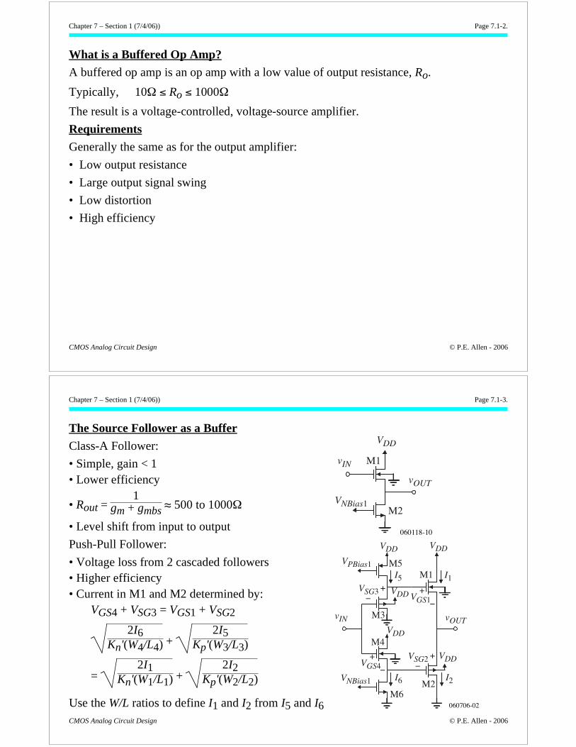
Crossover-Inverter, Buffer Stage Op Amp - Continued
How does the output buffer work? The two inverters, M1-M3 and M2-M4 are designed to work over different regions of the buffer input voltage, vin’. Consider the idealized voltage transfer characteristic of the crossover inverters:
060706-05
VDDVA
M6 Active
M6 Satur-ated
M5 Active
M5 Saturated
VB
M1-M3Inverter
M2-M4Inverter
0 vin'
M1 M2
M3 M4M7
vout
VDD
VSS
C2C1
vin'
M6
M5 RL
voutVDD
VSS
IBias
Crossover voltage VC = VB-VA 0 VC is designed to be small and positive for worst case variations in processing.
Chapter 7 – Section 1 (7/4/06)) Page 7.1-9.
CMOS Analog Circuit Design © P.E. Allen - 2006
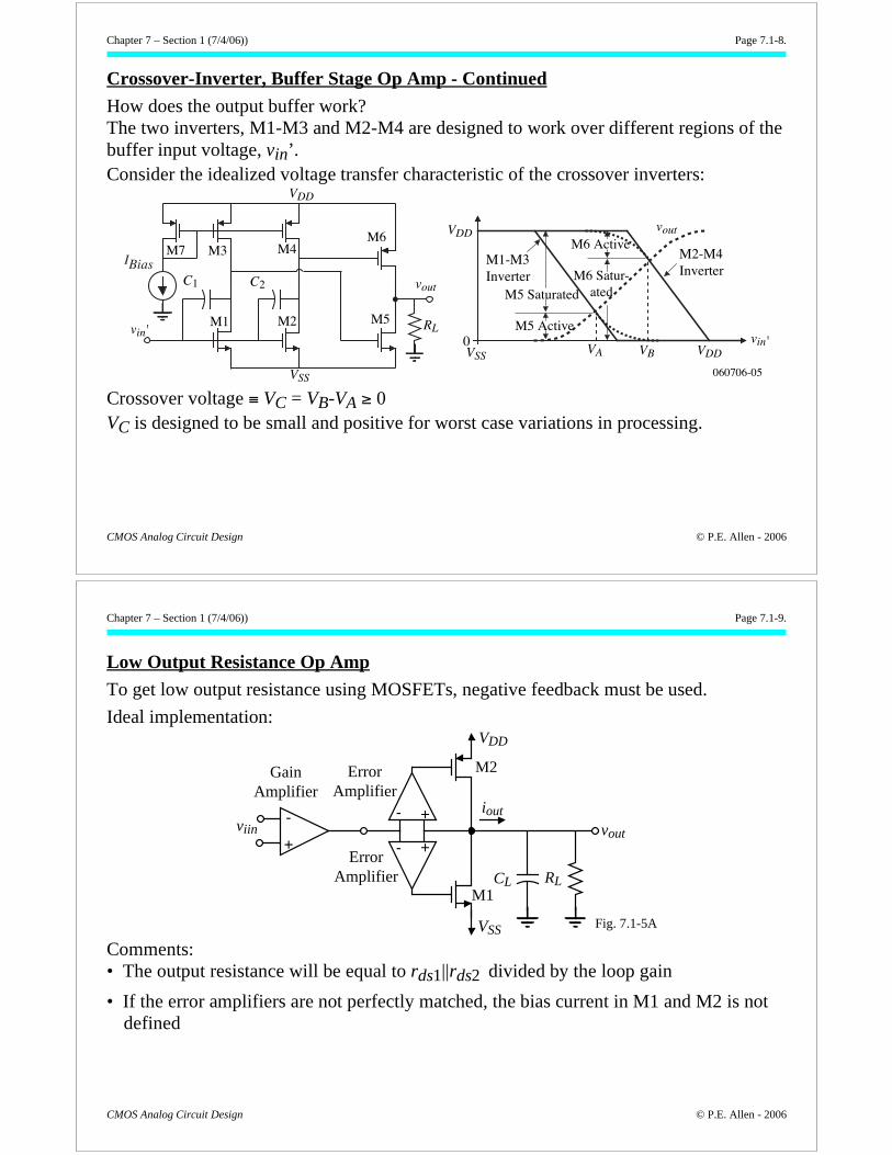
Low Output Resistance Op Amp
To get low output resistance using MOSFETs, negative feedback must be used.
Ideal implementation:
CL RL
viin vout
iout
VDD
M2
M1
Fig. 7.1-5A
+-
+-
ErrorAmplifier
ErrorAmplifier
VSS
+-
GainAmplifier
Comments: • The output resistance will be equal to rds1||rds2 divided by the loop gain
• If the error amplifiers are not perfectly matched, the bias current in M1 and M2 is not defined
Chapter 7 – Section 1 (7/4/06)) Page 7.1-10.
CMOS Analog Circuit Design © P.E. Allen - 2006
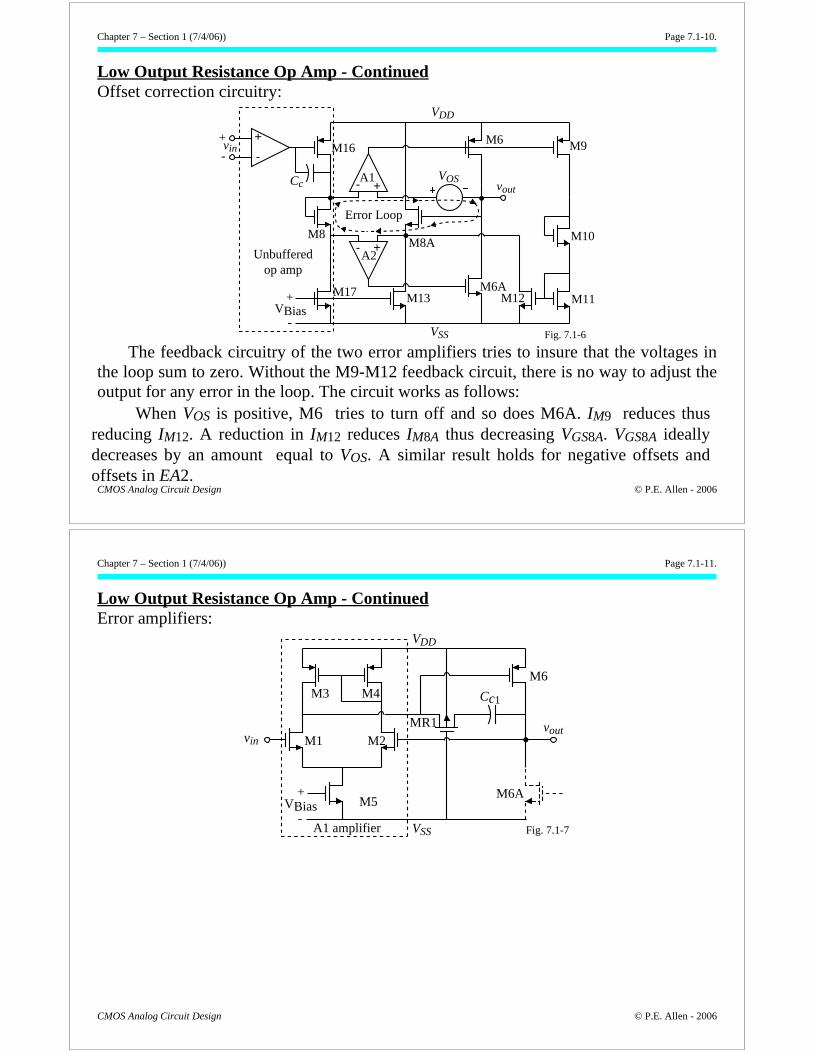
Low Output Resistance Op Amp - Continued Offset correction circuitry:
-
+vin
A1
M16 M9
vout
VDD
VSS
VBias+
-
Cc
+-
+-
+-M8
M17
M8A
M13M6A
M6
M12 M11
M10
A2
VOS
Error Loop
Fig. 7.1-6
Unbufferedop amp
The feedback circuitry of the two error amplifiers tries to insure that the voltages in the loop sum to zero. Without the M9-M12 feedback circuit, there is no way to adjust the output for any error in the loop. The circuit works as follows:
When VOS is positive, M6 tries to turn off and so does M6A. IM9 reduces thus reducing IM12. A reduction in IM12 reduces IM8A thus decreasing VGS8A. VGS8A ideally decreases by an amount equal to VOS. A similar result holds for negative offsets and offsets in EA2.
Chapter 7 – Section 1 (7/4/06)) Page 7.1-11.
CMOS Analog Circuit Design © P.E. Allen - 2006
Low Output Resistance Op Amp - Continued Error amplifiers:
vin M1 M2
M3 M4
M5
M6
M6A
vout
VDD
VSS
VBias+
-
Cc1
A1 amplifier
MR1
Fig. 7.1-7
Chapter 7 – Section 1 (7/4/06)) Page 7.1-12.
CMOS Analog Circuit Design © P.E. Allen - 2006
Low Output Resistance Op Amp - Complete Schematic
Short circuit protection(max. output ±60mA): MP3-MN3-MN4-MP4-MP5 MN3A-MP3A-MP4A-MN4A-MN5A
Rout rds6||rds6ALoop Gain
50k5000 = 10
M2
M3 M4
M5
M1
vout
VDD
VSS
VBiasN+
-
Cc
+-
VBiasP+
-
Cc1
M16M3H M4H MP4
MP3
MP5
MR1
M8
M17 MN3 MN4
M6
M6A
M13 M12 M11
MR2Cc2
M8A
M9
MN5A
MN4A
MN3A
MP4A
MP3A
M4HA
M4A M3A
M3HA
M1AM2A
M5Avin+
-
Fig. 7.1-8
M10
RC
R1 RL CL
CC
C1
gm1 gm6
Chapter 7 – Section 1 (7/4/06)) Page 7.1-13.
CMOS Analog Circuit Design © P.E. Allen - 2006
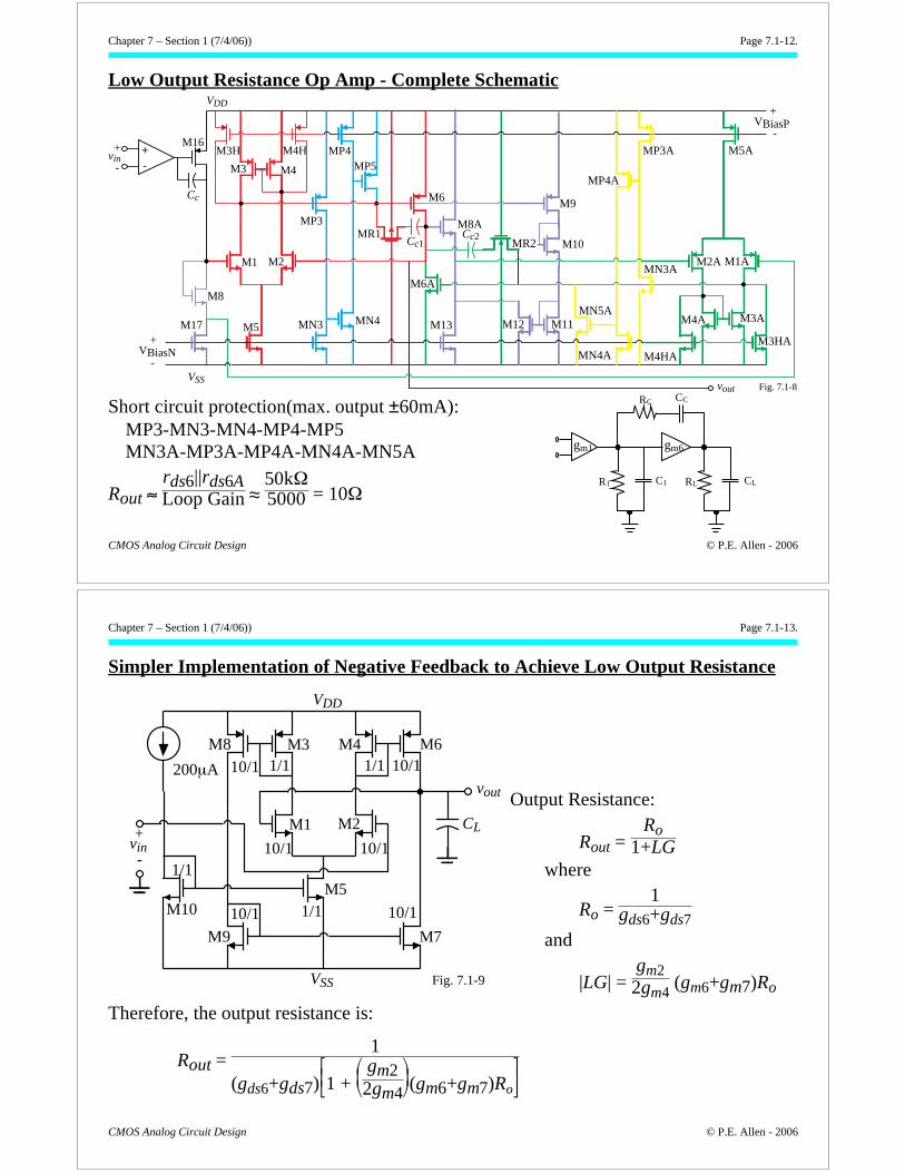
Simpler Implementation of Negative Feedback to Achieve Low Output Resistance Output Resistance:
Rout = Ro
1+LG
where
Ro = 1
gds6+gds7
and
|LG| = gm2
2gm4 (gm6+gm7)Ro
Therefore, the output resistance is:
Rout = 1
(gds6+gds7) 1 + gm2
2gm4 (gm6+gm7)Ro
-
+vin
M1 M2
M3 M4
M5
M6
M7
vout
VDD
VSS
CL
M8
M10
M9
Fig. 7.1-9
1/1 10/1200μA 10/1
10/1 10/1
1/1
1/1
1/1
10/1 10/1
Chapter 7 – Section 1 (7/4/06)) Page 7.1-14.
CMOS Analog Circuit Design © P.E. Allen - 2006
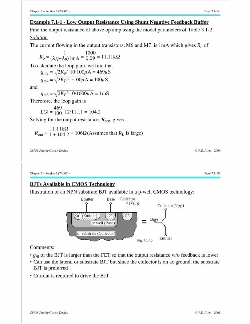
Example 7.1-1 - Low Output Resistance Using Shunt Negative Feedback Buffer
Find the output resistance of above op amp using the model parameters of Table 3.1-2.
Solution
The current flowing in the output transistors, M6 and M7, is 1mA which gives Ro of
Ro = 1
( N+ P)1mA = 10000.09 = 11.11k
To calculate the loop gain, we find that gm2 = 2KN’·10·100μA = 469μS
gm4 = 2KP’·1·100μA = 100μS
and gm6 = 2KP’·10·1000μA = 1mS
Therefore, the loop gain is
|LG| = 469100 12·11.11 = 104.2
Solving for the output resistance, Rout, gives
Rout = 11.11k1 + 104.2 = 106 (Assumes that RL is large)
Chapter 7 – Section 1 (7/4/06)) Page 7.1-15.
CMOS Analog Circuit Design © P.E. Allen - 2006
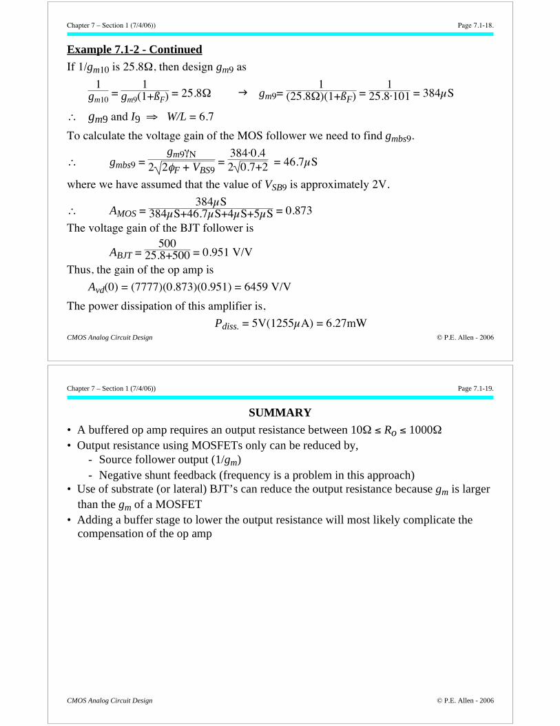
BJTs Available in CMOS Technology
Illustration of an NPN substrate BJT available in a p-well CMOS technology:
������
����
n- substrate (Collector)
p- well (Base)
n+ (Emitter) p+
��n+
Emitter Base Collector(VDD)
Collector (VDD)
Emitter
Base
Fig. 7.1-10 Comments:
• gm of the BJT is larger than the FET so that the output resistance w/o feedback is lower • Can use the lateral or substrate BJT but since the collector is on ac ground, the substrate
BJT is preferred
• Current is required to drive the BJT

Chapter 7 – Section 1 (7/4/06)) Page 7.1-16.
CMOS Analog Circuit Design © P.E. Allen - 2006
Two-Stage Op Amp with a Class-A BJT Output Buffer Stage Purpose of the M8-M9 source follower: 1.) Reduce the output resistance
(includes whatever is seen from the base to ground divided by 1+ F)
2.) Reduces the output load at the drains of M6 and M7
Small-signal output resistance :
Rout r 10 + (1/gm9)
1+ßF =
1gm10
+ 1
gm9(1+ßF)
= 51.6 +6.7 = 58.3 where I10=500μA, I8=100μA, W9/L9=100 and ßF is 100
M1 M2
M3 M4
M5
M6
M7
vout
VDD
VSS
CcCL
IBias
Q10
M11
M12
M13
Fig. 7.1-11
M8
M9
Output Buffer
RL
vin
+
-
vOUT(max) = VDD - VSD8(sat) - vBE10 = VDD - 2KP’
I8(W8/L8) - Vt lnIc10Is10
Voltage gain:
voutvin
gm1
gds2+gds4
gm6gds6+gds7
gm9gm9+gmbs9+gds8+g 10
gm10RL1+gm10RL
Compensation will be more complex because of the additional stages.
Chapter 7 – Section 1 (7/4/06)) Page 7.1-17.
CMOS Analog Circuit Design © P.E. Allen - 2006
Example 7.1-2 - Designing the Class-A, Buffered Op Amp Use the parameters of Table 3.1-2 along with the BJT parameters of Is = 10-14A and ßF = 100 to design the class-A, buffered op amp to give the following specifications. Assume the channel length is to be 1μm. VDD = 2.5V VSS = -2.5V GB = 5MHz Avd(0) 5000V/V Slew rate 10V/μs RL = 500 Rout 100 CL = 100pF ICMR = -1V to 2V Solution Because the specifications above are similar to the two-stage design of Ex. 6.3-1, we can use these results for the first two stages of our design. However, we must convert the results of Ex. 6.3-1 to a PMOS input stage. The results of doing this give W1= W2 = 6μm, W3 = W4 = 7μm, W5 = 11μm, W6 = 43μm, and W7 = 34μm. BJT follower: SR = 10V/μs and 100pF capacitor give I11 = 1mA.
If W13 = 44μm, then W11 = 44μm(1000μA/30μA) = 1467μm. I11 = 1mA 1/gm10 = 0.0258V/1mA = 25.8 MOS follower: To source 1mA, the BJT requires 20μA (ß =100) from the MOS follower. Therefore, select a bias current of 100μA for M8. If W12 = 44μm, then W8 = 44μm(100μA/30μA) = 146μm.
Chapter 7 – Section 1 (7/4/06)) Page 7.1-18.
CMOS Analog Circuit Design © P.E. Allen - 2006
Example 7.1-2 - Continued
If 1/gm10 is 25.8 , then design gm9 as
1
gm10 =
1gm9(1+ßF) = 25.8 gm9=
1(25.8 )(1+ßF) =
125.8·101 = 384μS
gm9 and I9 W/L = 6.7
To calculate the voltage gain of the MOS follower we need to find gmbs9.
gmbs9 = gm9 N
2 2 F + VBS9 =
384·0.42 0.7+2 = 46.7μS
where we have assumed that the value of VSB9 is approximately 2V.
AMOS = 384μS
384μS+46.7μS+4μS+5μS = 0.873
The voltage gain of the BJT follower is
ABJT = 500
25.8+500 = 0.951 V/V
Thus, the gain of the op amp is
Avd(0) = (7777)(0.873)(0.951) = 6459 V/V
The power dissipation of this amplifier is,
Pdiss. = 5V(1255μA) = 6.27mW
Chapter 7 – Section 1 (7/4/06)) Page 7.1-19.
CMOS Analog Circuit Design © P.E. Allen - 2006
SUMMARY
• A buffered op amp requires an output resistance between 10 Ro 1000
• Output resistance using MOSFETs only can be reduced by, - Source follower output (1/gm) - Negative shunt feedback (frequency is a problem in this approach)
• Use of substrate (or lateral) BJT’s can reduce the output resistance because gm is larger than the gm of a MOSFET
• Adding a buffer stage to lower the output resistance will most likely complicate the compensation of the op amp
Chapter 7 – Section 2 (7/4/06)) Page 7.2-1.
CMOS Analog Circuit Design © P.E. Allen - 2006
SECTION 7.2 – HIGH SPEED/FREQUENCY OP AMPS Objective
The objective of this presentation is:
1.) Increase the GB of operational amplifiers
2.) Cascading of Amplifiers
Outline
• Extending the GB of conventional op amps
• Cascade Amplifiers
- Voltage amplifiers
- Voltage amplifiers using current feedback
Chapter 7 – Section 2 (7/4/06)) Page 7.2-2.
CMOS Analog Circuit Design © P.E. Allen - 2006
INCREASING THE GB OF OP AMPS
What is the Influence of GB on the Frequency Response? The unity-gainbandwidth represents a limit in the trade-off between closed loop voltage gain and the closed-loop -3dB frequency. Example of a gain of -10 voltage amplifier:
0dB
20dB
|Avd(0)| dB
Magnitude
log10(ω)GBωA ω-3dB
Op amp frequency response
Amplifier with a gain of -10
Fig. 7.2-1 What causes the GB? We know that
GB = gmC
where gm is the transconductance that converts the input voltage to current and C is the capacitor that causes the dominant pole. This relationship assumes that all higher-order poles are greater than GB.
Chapter 7 – Section 2 (7/4/06)) Page 7.2-3.
CMOS Analog Circuit Design © P.E. Allen - 2006
What is the Limit of GB? The following illustrates what happens when the next higher pole is not greater than GB:
For a two-stage op amp, the poles and zeros are:
1.) Dominant pole p1 = -gm1
Av(0)Cc
2.) Output pole p2 = -gm6CL
3.) Mirror pole p3 = -gm3
Cgs3+Cgs4 and z3 = 2p3
4.) Nulling pole p4 = -1
RzCI
5.) Nulling zero z1 = -1
RzCc-(Cc/gm6)
0dB
20dB
|Avd(0)| dB
Magnitude
log10(ω)GBωA ω-3dB
Op amp frequency response
Amplifier with a gain of -10
Fig. 7.2-2
Next higher pole-40dB/dec
Chapter 7 – Section 2 (7/4/06)) Page 7.2-4.
CMOS Analog Circuit Design © P.E. Allen - 2006
Higher-Order Poles
For reasonable phase margin, the smallest higher-order pole should be 2-3 times larger than GB if all other higher-order poles are larger than 10GB.
060709-01
-GB-10GB
Dominantpole
Smallest non-dominant pole
Larger non-dominant poles
GB
10GB0dB
Av(0) dB
GBAv(0)
log10ω
If the higher-order poles are not greater than 10GB, then the distance from GB to the smallest non-dominant pole should be increased for reasonable phase margin.
Chapter 7 – Section 2 (7/4/06)) Page 7.2-5.
CMOS Analog Circuit Design © P.E. Allen - 2006
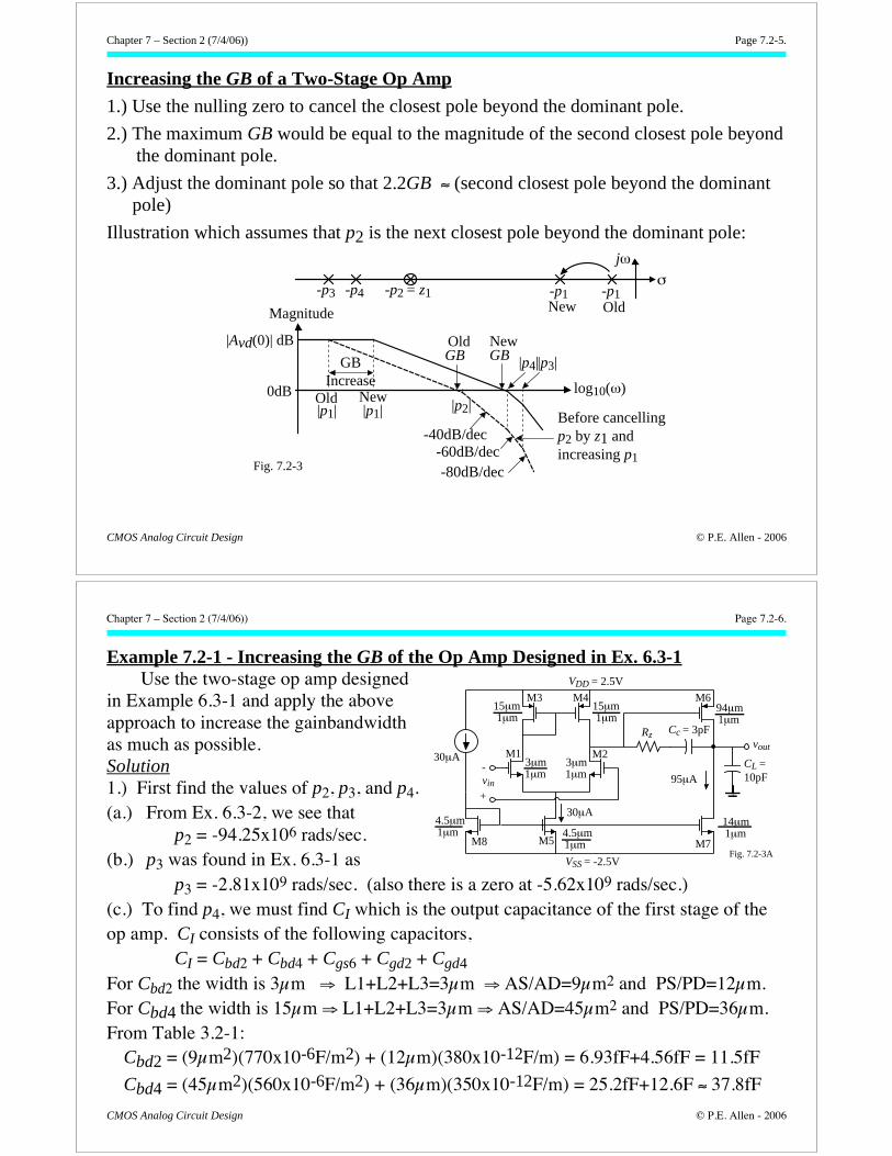
Increasing the GB of a Two-Stage Op Amp
1.) Use the nulling zero to cancel the closest pole beyond the dominant pole.
2.) The maximum GB would be equal to the magnitude of the second closest pole beyond the dominant pole.
3.) Adjust the dominant pole so that 2.2GB (second closest pole beyond the dominant pole)
Illustration which assumes that p2 is the next closest pole beyond the dominant pole:
0dB
|Avd(0)| dB
Magnitude
log10(ω)
Fig. 7.2-3
-40dB/dec
-p1-p2 = z1-p4-p3
|p1| |p2|
|p4||p3|
-60dB/dec-80dB/dec
Before cancellingp2 by z1 and increasing p1
jωσ
|p1|
GB
-p1New Old
GBIncrease
OldGBNew
Old New
Chapter 7 – Section 2 (7/4/06)) Page 7.2-6.
CMOS Analog Circuit Design © P.E. Allen - 2006
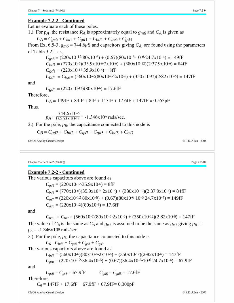
Example 7.2-1 - Increasing the GB of the Op Amp Designed in Ex. 6.3-1 Use the two-stage op amp designed in Example 6.3-1 and apply the above approach to increase the gainbandwidth as much as possible. Solution 1.) First find the values of p2, p3, and p4. (a.) From Ex. 6.3-2, we see that
p2 = -94.25x10⁶ rads/sec. (b.) p3 was found in Ex. 6.3-1 as
p3 = -2.81x10⁹ rads/sec. (also there is a zero at -5.62x10⁹ rads/sec.) (c.) To find p4, we must find CI which is the output capacitance of the first stage of the op amp. CI consists of the following capacitors, CI = Cbd2 + Cbd4 + Cgs6 + Cgd2 + Cgd4 For Cbd2 the width is 3μm L1+L2+L3=3μm AS/AD=9μm2 and PS/PD=12μm. For Cbd4 the width is 15μm L1+L2+L3=3μm AS/AD=45μm2 and PS/PD=36μm. From Table 3.2-1: Cbd2 = (9μm2)(770x10-6F/m2) + (12μm)(380x10-12F/m) = 6.93fF+4.56fF = 11.5fF
Cbd4 = (45μm2)(560x10-6F/m2) + (36μm)(350x10-12F/m) = 25.2fF+12.6F 37.8fF
-
+vin
M1 M2
M3 M4
M5
M6
M7
vout
VDD = 2.5V
VSS = -2.5V
Cc = 3pF
CL =10pF
3μm1μm
3μm1μm
15μm1μm
15μm1μm
M84.5μm1μm
30μA
4.5μm1μm
14μm1μm
94μm1μm
30μA
95μA
Fig. 7.2-3A
Rz

Chapter 7 – Section 2 (7/4/06)) Page 7.2-7.
CMOS Analog Circuit Design © P.E. Allen - 2006
Example 7.2-1 - Continued
Cgs6 is given by Eq. (10b) of Sec. 3.2 and is Cgs6=CGDO·W6+0.67(CoxW6L6)=(220x10-12)(94x10-6)+(0.67)(24.7x10⁻⁴)(94x10-12) = 20.7fF + 154.8fF = 175.5fF Cgd2 = 220x10-12x3μm = 0.66fF and Cgd4 = 220x10-12x15μm = 3.3fF Therefore, CI = 11.5fF + 37.8fF + 175.5fF + 0.66fF + 3.3fF = 228.8fF. Although Cbd2 and Cbd4 will be reduced with a reverse bias, let us use these values to provide a margin. In fact, we probably ought to double the whole capacitance to make sure that other layout parasitics are included. Thus let CI be 300fF. In Ex. 6.3-2, Rz was 4.591k which gives p4 = - 0.726x10⁹ rads/sec. 2.) Using the nulling zero, z1, to cancel p2, gives p4 as the next smallest pole. For 60° phase margin GB = |p4|/2.2 if the next smallest pole is more than 10GB.
GB = 0.726x10⁹/2.2 = 0.330x10⁹ rads/sec. or 52.5MHz. This value of GB is designed from the relationship that GB = gm1/Cc. Assuming gm1 is
constant, then Cc = gm1/GB = (94.25x10⁻⁶)/(0.330x109) = 286fF. It might be useful to increase gm1 in order to keep Cc above the surrounding parasitic capacitors (Cgd6 = 20.7fF). The success of this method assumes that there are no other roots with a magnitude smaller than 10GB.
Chapter 7 – Section 2 (7/4/06)) Page 7.2-8.
CMOS Analog Circuit Design © P.E. Allen - 2006
Example 7.2-2 - Increasing the GB of the Folded Cascode Op Amp of Ex. 6.5-3 Use the folded-cascode op amp designed in Example 6.5-3 and apply the above approach to increase the gainbandwidth as much as possible. Assume that the drain/source areas are equal to 2μm times the width of the transistor and that all voltage dependent capacitors are at zero voltage. Solution The poles of the folded cascode op amp are:
pA -1
RACA (the pole at the source of M6 )
pB -1
RBCB (the pole at the source of M7)
p6 -gm10
C6 (the pole at the drain of M6)
p8 -gm8rds8gm10
C8 (the pole at the source of M8)
p9 -gm9C9 (the pole at the source of M9)
060628-04
VPB1
M4 M5
RAI6
VPB2 RB
I4 I5
VDD
I7M6 M7
VNB2
M8 M9
M10 M11
+−
vIN
vOUT
VNB1
I1 I2
M1 M2
M3I3
CL
Chapter 7 – Section 2 (7/4/06)) Page 7.2-9.
CMOS Analog Circuit Design © P.E. Allen - 2006
Example 7.2-2 - Continued Let us evaluate each of these poles. 1,) For pA, the resistance RA is approximately equal to gm6 and CA is given as CA = Cgs6 + Cbd1 + Cgd1 + Cbd4 + Cbs6 + Cgd4
From Ex. 6.5-3, gm6 = 744.6μS and capacitors giving CA are found using the parameters of Table 3.2-1 as, Cgs6 = (220x10-12·80x10-6) + (0.67)(80x10-6·10-6·24.7x10-4) = 149fF Cbd1 = (770x10-6)(35.9x10-6·2x10-6) + (380x10-12)(2·37.9x10-6) = 84fF Cgd1 = (220x10-12·35.9x10-6) = 8fF Cbd4 = Cbs6 = (560x10-6)(80x10-6·2x10-6) + (350x10-12)(2·82x10-6) = 147fF and Cgd4 = (220x10-12)(80x10-6) = 17.6fF Therefore, CA = 149fF + 84fF + 8fF + 147fF + 17.6fF + 147fF = 0.553pF Thus,
pA = -744.6x10⁻⁶
0.553x10-12 = -1.346x10⁹ rads/sec.
2.) For the pole, pB, the capacitance connected to this node is
CB = Cgd2 + Cbd2 + Cgs7 + Cgd5 + Cbd5 + Cbs7
Chapter 7 – Section 2 (7/4/06)) Page 7.2-10.
CMOS Analog Circuit Design © P.E. Allen - 2006
Example 7.2-2 - Continued The various capacitors above are found as Cgd2 = (220x10-12·35.9x10-6) = 8fF Cbd2 = (770x10-6)(35.9x10-6·2x10-6) + (380x10-12)(2·37.9x10-6) = 84fF
Cgs7 = (220x10-12·80x10-6) + (0.67)(80x10-6·10-6·24.7x10-4) = 149fF Cgd5 = (220x10-12)(80x10-6) = 17.6fF and Cbd5 = Cbs7 = (560x10-6)(80x10-6·2x10-6) + (350x10-12)(2·82x10-6) = 147fF The value of CB is the same as CA and gm6 is assumed to be the same as gm7 giving pB = pA = -1.346x10⁹ rads/sec. 3.) For the pole, p6, the capacitance connected to this node is C6= Cbd6 + Cgd6 + Cgs8 + Cgs9 The various capacitors above are found as Cbd6 = (560x10-6)(80x10-6·2x10-6) + (350x10-12)(2·82x10-6) = 147fF Cgs8 = (220x10-12·36.4x10-6) + (0.67)(36.4x10-6·10-6·24.7x10-4) = 67.9fF and Cgs9 = Cgs8 = 67.9fF Cgd6 = Cgd5 = 17.6fF Therefore, C6 = 147fF + 17.6fF + 67.9fF + 67.9fF= 0.300pF
Chapter 7 – Section 2 (7/4/06)) Page 7.2-11.
CMOS Analog Circuit Design © P.E. Allen - 2006
Example 7.2-2 - Continued From Ex. 6.5-3, gm6 = 744.6x10⁻⁶. Therefore, p6, can be expressed as
-p6 = 744.6x10⁻⁶
0.300x10-12 = 2.482x10⁹ rads/sec.
4.) Next, we consider the pole, p8. The capacitance connected to this node is C8= Cbd10 + Cgd10 + Cgs8 + Cbs8 These capacitors are given as, Cbs8 = Cbd10 = (770x10-6)(36.4x10-6·2x10-6) + (380x10-12)(2·38.4x10-6) = 85.2fF
Cgs8 = (220x10-12·36.4x10-6) + (0.67)(36.4x10-6·10-6·24.7x10-4) = 67.9fF and Cgd10 = (220x10-12)(36.4x10⁻⁶) = 8fF The capacitance C8 is equal to C8 = 67.9fF + 8fF + 85.2fF + 85.2fF = 0.246pF Using the values of Ex. 6.5-3 of 774.6μS, the pole p8 is found as,
-p8 = gm8rds8 gm10/C8 = -774.6μS·774.6μS·/3μS·0.246pF = - 812.4x10⁹ rads/sec.
5.) The capacitance for the pole at p9 is identical with C8. Therefore, since gm9 is 774.6μS, the pole p9 is found to be -p9 = 3.149x10⁹ rads/sec.
Chapter 7 – Section 2 (7/4/06)) Page 7.2-12.
CMOS Analog Circuit Design © P.E. Allen - 2006
Example 7.2-2 - Continued The poles are summarized below:
pA = -1.346x10⁹ rads/sec pB = -1.346x10⁹ rads/sec p6 = -2.482x10⁹ rads/sec
p8 = -812.4x10⁹ rads/sec p9 = -3.149x10⁹ rads/sec
The smallest of these poles is pA or pB. Since p6 and p9 are not much larger than pA or pB, we will find the new GB by dividing pA or pB by 6 (rather than 2.2) to get 224x106 rads/sec 200x106. Thus the new GB will be 200/2 or 32MHz. The magnitude of the dominant pole is given as
pdominant = GB
Avd(0) = 200x1067,464 = 26,795 rads/sec.
The value of load capacitor that will give this pole is
CL = 1
pdominant·Rout =
126.795x103·19.4M 1.9pF
Therefore, the new GB = 32MHz compared with the old GB = 10MHz.
Chapter 7 – Section 2 (7/4/06)) Page 7.2-13.
CMOS Analog Circuit Design © P.E. Allen - 2006
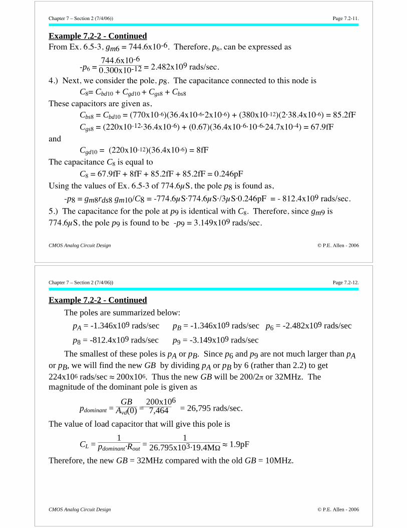
Elimination of Higher-Order Poles
The minimum circuitry for a cascode op amp is shown below:
060710-01
vin + VNB1
vin + VPB1
VNB2
VPB2
VDD
M1
M2
M3
M4
vout
CL
Dominant Pole
Non-dominant
Pole
Non-dominant
Pole
If the source-drain area between M1 and M2 and M3 and M4 can be minimized, the non-dominant poles will be quite large.
Chapter 7 – Section 2 (7/4/06)) Page 7.2-14.
CMOS Analog Circuit Design © P.E. Allen - 2006
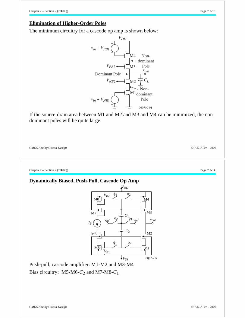
Dynamically Biased, Push-Pull, Cascode Op Amp
M1
M2
M3
M4
M6
M7
vout
VDD
VSS
C1
M5
M8
C2
vin+IB
φ1
φ1
φ1 φ2
φ2
φ2
vin-
+-VB2
+-VB1
Fig.7.2-5 Push-pull, cascode amplifier: M1-M2 and M3-M4
Bias circuitry: M5-M6-C2 and M7-M8-C1
Chapter 7 – Section 2 (7/4/06)) Page 7.2-15.
CMOS Analog Circuit Design © P.E. Allen - 2006
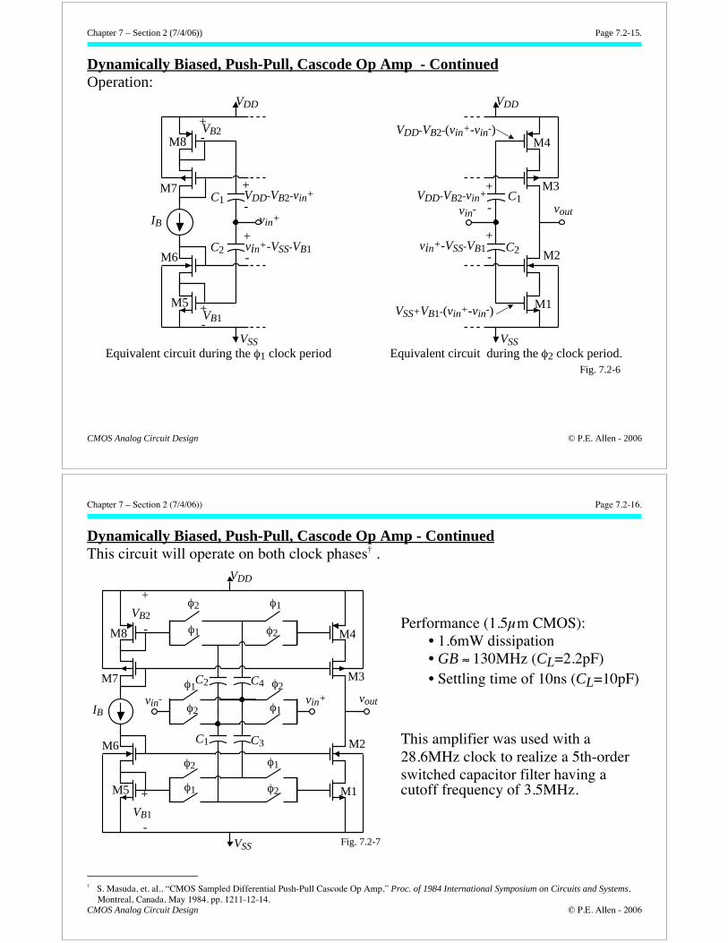
Dynamically Biased, Push-Pull, Cascode Op Amp - Continued Operation:
M6
M7
VDD
VSS
C1
M5
M8
C2
vin+IB
+-VB2
+-VB1
+
-VDD-VB2-vin+
+
-vin+-VSS-VB1
M1
M2
M3
M4
vout
VDD
VSS
C1
C2
vin-
+
-VDD-VB2-vin+
+
-vin+-VSS-VB1
VDD-VB2-(vin+-vin-)
VSS+VB1-(vin+-vin-)
Equivalent circuit during the φ1 clock period Equivalent circuit during the φ2 clock period.Fig. 7.2-6
Chapter 7 – Section 2 (7/4/06)) Page 7.2-16.
CMOS Analog Circuit Design © P.E. Allen - 2006
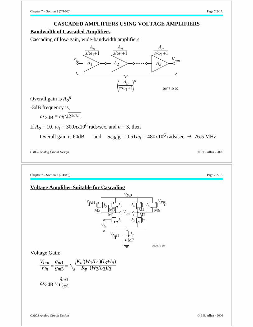
Dynamically Biased, Push-Pull, Cascode Op Amp - Continued This circuit will operate on both clock phases† .
† S. Masuda, et. al., “CMOS Sampled Differential Push-Pull Cascode Op Amp,” Proc. of 1984 International Symposium on Circuits and Systems,
Montreal, Canada, May 1984, pp. 1211-12-14.
M1
M2
M3
M4
M6
M7
vout
VDD
VSS
C1
M5
M8
C2
vin+IB φ2
φ1
φ1
φ1vin-
+
-VB2
+
-VB1
Fig. 7.2-7
C4
C3
φ2
φ2
φ2 φ1
φ1 φ2
φ2 φ1
Performance (1.5μm CMOS): • 1.6mW dissipation • GB 130MHz (CL=2.2pF) • Settling time of 10ns (CL=10pF)
This amplifier was used with a 28.6MHz clock to realize a 5th-order switched capacitor filter having a cutoff frequency of 3.5MHz.
Chapter 7 – Section 2 (7/4/06)) Page 7.2-17.
CMOS Analog Circuit Design © P.E. Allen - 2006
CASCADED AMPLIFIERS USING VOLTAGE AMPLIFIERS
Bandwidth of Cascaded Amplifiers
Cascading of low-gain, wide-bandwidth amplifiers:
060710-02
Ao s/ω1+1
Vin Vout
Ao s/ω1+1
Ao s/ω1+1
A1 A2 An
Ao s/ω1+1
n
Overall gain is Aon
-3dB frequency is,
-3dB = 1 21/n-1
If Ao = 10, 1 = 300 x106 rads/sec. and n = 3, then
Overall gain is 60dB and -3dB = 0.51 1 = 480x106 rads/sec. 76.5 MHz
Chapter 7 – Section 2 (7/4/06)) Page 7.2-18.
CMOS Analog Circuit Design © P.E. Allen - 2006
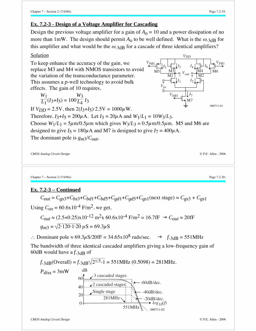
Voltage Amplifier Suitable for Cascading
060710-03
VDD
Vout +−
Vin+
−
Μ1 Μ2Μ3 Μ4Μ5
VNB1
VPB1 VPB1
Μ6
Μ7
I7
I3 I4I5 I6
I1 I2
Voltage Gain:
VoutVin =
gm1gm3 =
Kn'(W1/L1)(I3+I5)Kp' (W3/L3)I3
-3dB gm3Cgs1
Chapter 7 – Section 2 (7/4/06)) Page 7.2-19.
CMOS Analog Circuit Design © P.E. Allen - 2006
Ex. 7.2-3 - Design of a Voltage Amplifier for Cascading
Design the previous voltage amplifier for a gain of Ao = 10 and a power dissipation of no more than 1mW. The design should permit Ao to be well defined. What is the -3dB for this amplifier and what would be the -3dB for a cascade of three identical amplifiers?
Solution
To keep enhance the accuracy of the gain, we replace M3 and M4 with NMOS transistors to avoid the variation of the transconductance parameter. This assumes a p-well technology to avoid bulk effects. The gain of 10 requires,
W1L1 (I3+I5) = 100
W3L4 I3
If VDD = 2.5V, then 2(I3+I5)·2.5V = 1000μW. Therefore, I3+I5 = 200μA. Let I3 = 20μA and W1/L1 = 10W3/L3. Choose W1/L1 = 5μm/0.5μm which gives W3/L3 = 0.5μm/0.5μm. M5 and M6 are designed to give I5 = 180μA and M7 is designed to give I7 = 400μA. The dominant pole is gm3/Cout.
060711-01
VDD
Vout +−
Vin+
−
Μ1 Μ2Μ3 Μ4Μ5
VNB1
VPB1 VPB1
Μ6
Μ7
I7
I3 I4I5 I6
I1 I2
Chapter 7 – Section 2 (7/4/06)) Page 7.2-20.
CMOS Analog Circuit Design © P.E. Allen - 2006
Ex. 7.2-3 – Continued
Cout = Cgs3+Cbs3+Cbd1+Cbd5+Cgd1+Cgd5+Cgs1(next stage) Cgs3 + Cgs1
Using Cox = 60.6x10⁻⁴ F/m2, we get,
Cout (2.5+0.25)x10-12 m2x 60.6x10-4 F/m2 = 16.7fF Cout 20fF
gm3 = 2·120·1·20 μS = 69.3μS
Dominant pole 69.3μS/20fF = 34.65x10⁸ rads/sec. f-3dB = 551MHz
The bandwidth of three identical cascaded amplifiers giving a low-frequency gain of 60dB would have a f-3dB of
f-3dB(Overall) = f-3dB 21/3-1 = 551MHz (0.5098) = 281MHz.
Pdiss = 3mW
060711-02
log10(f)
dB
60
40
20
0
-60dB/dec.
-40dB/dec.
-20dB/dec.
551MHz
281MHz
3 cascaded stages
2 cascaded stages
Single stage

Chapter 7 – Section 2 (7/4/06)) Page 7.2-21.
CMOS Analog Circuit Design © P.E. Allen - 2006
A 71 MHz CMOS Programmable Gain Amplifier† Uses 3 ac-coupled stages. First stage (0-20dB, common gate for impedance matching and NF):
vout
VDD
vout
CMFB
VBP
VBN
0dB2dB
VB1
vin
VB1
vin
0dB 2dB
M2dB M0dB M2dBM0dB
M2 M2
M3
Fig. 7.2-137A Rin = 330 to match source driving requirement All current sinks are identical for the differential switches.
Dominant pole at 150MHz.
† P. Orsatti, F. Piazza, and Q. Huang, “A 71 MHz CMOS IF-Basdband Strip for GSM, IEEE JSSC, vol. 35, No. 1, Jan. 2000, pp. 104-108.
Chapter 7 – Section 2 (7/4/06)) Page 7.2-22.
CMOS Analog Circuit Design © P.E. Allen - 2006
A 71 MHz PGA – Continued Second stage (-10dB to 20dB):
M2 M2
M3
M2 M2
M3
CMFB
-10dB
-10dB
vout vout
VBP
VBN
vin vin
Fig. 7.2-137A
M5
M4
M6
M2dB M0dB
0dBLoad -10dB
Load
M5
M4
M6
M2dBM0dB
0dB 2dB0dB2dB
VDD
Dominant pole is also at 150MHz For VDD = 2.5V, at 60dB gain, the total current is 2.6mA
IIP3 +1dBm
Chapter 7 – Section 2 (7/4/06)) Page 7.2-23.
CMOS Analog Circuit Design © P.E. Allen - 2006
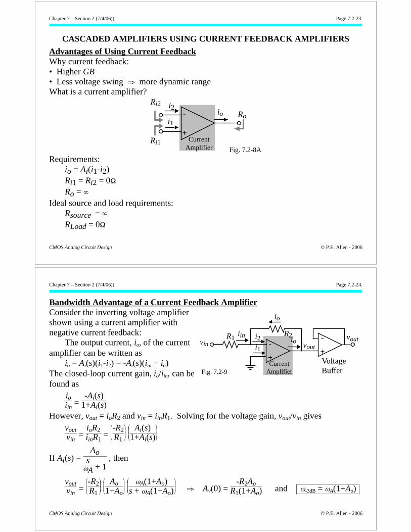
CASCADED AMPLIFIERS USING CURRENT FEEDBACK AMPLIFIERS
Advantages of Using Current Feedback Why current feedback: • Higher GB • Less voltage swing more dynamic range What is a current amplifier?
Ri2
i1
i2io
+
-
CurrentAmplifier
Ri1
Ro
Fig. 7.2-8A Requirements: io = Ai(i1-i2) Ri1 = Ri2 = 0 Ro =
Ideal source and load requirements: Rsource = RLoad = 0
Chapter 7 – Section 2 (7/4/06)) Page 7.2-24.
CMOS Analog Circuit Design © P.E. Allen - 2006
Bandwidth Advantage of a Current Feedback Amplifier Consider the inverting voltage amplifier shown using a current amplifier with negative current feedback:
The output current, io, of the current amplifier can be written as io = Ai(s)(i1-i2) = -Ai(s)(iin + io) The closed-loop current gain, io/iin, can be found as
ioiin =
-Ai(s)1+Ai(s)
However, vout = ioR2 and vin = iinR1. Solving for the voltage gain, vout/vin gives
voutvin
= ioR2iinR1
= -R2R1
Ai(s)
1+Ai(s)
If Ai(s) = Ao
sA + 1
, then
voutvin
= -R2R1
Ao
1+Ao
A(1+Ao)s + A(1+Ao) Av(0) =
-R2AoR1(1+Ao) and -3dB = A(1+Ao)
vinvout
+-
+-
i1
i2 io
io
vout
CurrentAmplifier
R1R2iin
VoltageBufferFig. 7.2-9
Chapter 7 – Section 2 (7/4/06)) Page 7.2-25.
CMOS Analog Circuit Design © P.E. Allen - 2006
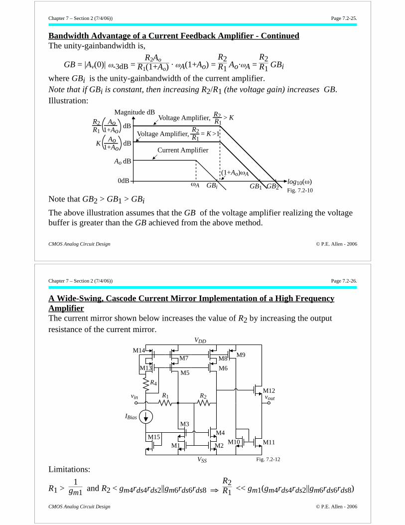
Bandwidth Advantage of a Current Feedback Amplifier - Continued The unity-gainbandwidth is,
GB = |Av(0)| -3dB = R2Ao
R1(1+Ao) · A(1+Ao) = R2R1
Ao· A = R2R1
GBi
where GBi is the unity-gainbandwidth of the current amplifier. Note that if GBi is constant, then increasing R2/R1 (the voltage gain) increases GB. Illustration:
Ao dB
ωA
R2R1
>1
R2R1
GB1 GB2
Current Amplifier
0dB
Voltage Amplifier,
log10(ω)
Magnitude dB
Fig. 7.2-10
(1+Ao)ωA
GBi
= K
R1Voltage Amplifier, > KR2
1+AoAo dB
1+AoAo dBK
Note that GB2 > GB1 > GBi
The above illustration assumes that the GB of the voltage amplifier realizing the voltage buffer is greater than the GB achieved from the above method.
Chapter 7 – Section 2 (7/4/06)) Page 7.2-26.
CMOS Analog Circuit Design © P.E. Allen - 2006
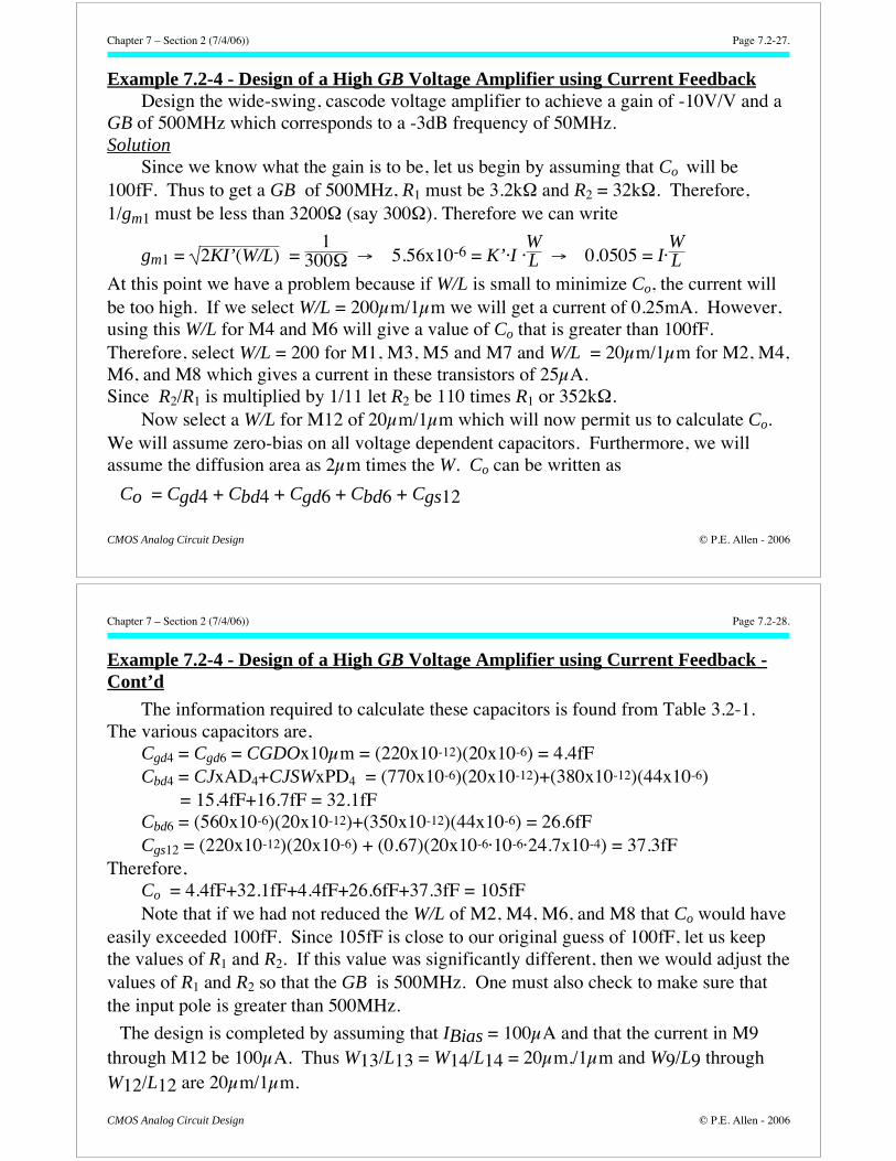
A Wide-Swing, Cascode Current Mirror Implementation of a High Frequency Amplifier The current mirror shown below increases the value of R2 by increasing the output resistance of the current mirror.
vin
M2
M6
M4
M5
vout
VDD
VSS
R2
M13
M14
R1
M3
M1
IBias
M7 M8 M9
M10 M11
M12R4
Fig. 7.2-12
M15
Limitations:
R1 > 1
gm1 and R2 < gm4rds4rds2||gm6rds6rds8
R2R1
<< gm1(gm4rds4rds2||gm6rds6rds8)
Chapter 7 – Section 2 (7/4/06)) Page 7.2-27.
CMOS Analog Circuit Design © P.E. Allen - 2006
Example 7.2-4 - Design of a High GB Voltage Amplifier using Current Feedback Design the wide-swing, cascode voltage amplifier to achieve a gain of -10V/V and a GB of 500MHz which corresponds to a -3dB frequency of 50MHz. Solution Since we know what the gain is to be, let us begin by assuming that Co will be 100fF. Thus to get a GB of 500MHz, R1 must be 3.2k and R2 = 32k . Therefore, 1/gm1 must be less than 3200 (say 300 ). Therefore we can write
gm1 = 2KI’(W/L) = 1
300 5.56x10-6 = K’·I ·WL 0.0505 = I·
WL
At this point we have a problem because if W/L is small to minimize Co, the current will be too high. If we select W/L = 200μm/1μm we will get a current of 0.25mA. However, using this W/L for M4 and M6 will give a value of Co that is greater than 100fF. Therefore, select W/L = 200 for M1, M3, M5 and M7 and W/L = 20μm/1μm for M2, M4, M6, and M8 which gives a current in these transistors of 25μA. Since R2/R1 is multiplied by 1/11 let R2 be 110 times R1 or 352k . Now select a W/L for M12 of 20μm/1μm which will now permit us to calculate Co. We will assume zero-bias on all voltage dependent capacitors. Furthermore, we will assume the diffusion area as 2μm times the W. Co can be written as
Co = Cgd4 + Cbd4 + Cgd6 + Cbd6 + Cgs12
Chapter 7 – Section 2 (7/4/06)) Page 7.2-28.
CMOS Analog Circuit Design © P.E. Allen - 2006
Example 7.2-4 - Design of a High GB Voltage Amplifier using Current Feedback - Cont’d
The information required to calculate these capacitors is found from Table 3.2-1. The various capacitors are, Cgd4 = Cgd6 = CGDOx10μm = (220x10-12)(20x10-6) = 4.4fF Cbd4 = CJxAD4+CJSWxPD4 = (770x10-6)(20x10-12)+(380x10-12)(44x10-6)
= 15.4fF+16.7fF = 32.1fF Cbd6 = (560x10-6)(20x10-12)+(350x10-12)(44x10-6) = 26.6fF Cgs12 = (220x10-12)(20x10-6) + (0.67)(20x10-6·10-6·24.7x10-4) = 37.3fF Therefore, Co = 4.4fF+32.1fF+4.4fF+26.6fF+37.3fF = 105fF Note that if we had not reduced the W/L of M2, M4, M6, and M8 that Co would have easily exceeded 100fF. Since 105fF is close to our original guess of 100fF, let us keep the values of R1 and R2. If this value was significantly different, then we would adjust the values of R1 and R2 so that the GB is 500MHz. One must also check to make sure that the input pole is greater than 500MHz.
The design is completed by assuming that IBias = 100μA and that the current in M9 through M12 be 100μA. Thus W13/L13 = W14/L14 = 20μm,/1μm and W9/L9 through W12/L12 are 20μm/1μm.

Chapter 7 – Section 2 (7/4/06)) Page 7.2-29.
CMOS Analog Circuit Design © P.E. Allen - 2006
Example 7.2-4 - Continued
Frequency (Hz)
|vou
t/vin
| dB
Fig. 7.2-13
-30
-20
-10
0
10
20
30
105 106 107 108 109 1010
f-3dB GB
-20dB/dec
-40dB/dec
R1 = 3.2kΩ
R1 = 1kΩ
Simulation Results: f-3dB 38MHz GB 300MHz Closed-loop gain = 18dB
(Loss of -2dB is attributed to source follower and R1) Note second pole at about 1GHz. To get these results, it was necessary to bias the input at -1.7VDC using ±3V power supplies. If R1 is decreased to 1k results in:
Gain of 26.4dB, f-3dB = 32MHz, and GB = 630MHz
Chapter 7 – Section 2 (7/4/06)) Page 7.2-30.
CMOS Analog Circuit Design © P.E. Allen - 2006
Current Feedback Amplifier
The difficulties of making the input resistance of the current amplifier small compared to R1 can be solved with the following block diagram:
060711-04
GMAi
RF
VinVout
+
−
VoutVin =
-GMRFAi1 +Ai

Chapter 7 – Section 2 (7/4/06)) Page 7.2-31.
CMOS Analog Circuit Design © P.E. Allen - 2006
Differential Implementation of the Current Feedback Amplifier VDD
060712-01
Rin
RF RF+ −Vout
VPB1
VPB2
VNB2
M1 M2
1:n 1:n
Vin+ Vin
-
Iin = gm1
1+ 0.5gm1Rin Vin
+- Vin-
2 and Vout = n (2RF)
1+n Iin
VoutVin
2nRFRin
Chapter 7 – Section 2 (7/4/06)) Page 7.2-32.
CMOS Analog Circuit Design © P.E. Allen - 2006
A 20dB Voltage Amplifier using a Current Amplifier
The following circuit is a programmable voltage amplifier with up to 20dB gain:
M1
VDD
VSS
R1
+1 +1
VBias
+ -vout
vin+ vin-
M2
x2= 1/4
x4=1/8
x2= 1/4
x4=1/8
x1=1/2
x1=1/2
R2 R2
Fig. 7.2-135A R1 and the current mirrors are used for gain variation while R2 is fixed.

Chapter 7 – Section 2 (7/4/06)) Page 7.2-33.
CMOS Analog Circuit Design © P.E. Allen - 2006
Programmability of the Previous Stage
Input OTA:
Changes GM in 6dB steps.
Chapter 7 – Section 2 (7/4/06)) Page 7.2-34.
CMOS Analog Circuit Design © P.E. Allen - 2006
Programmability of the Voltage Stage – Cont’d
Current Amplifier:
Changes RF in 2dB steps (RF20dB = 2.1k , RF18dB = 1.6k , RF16dB = 1.3k , and RF14dB = 5k .
RFTotal = 10k .

Chapter 7 – Section 2 (7/4/06)) Page 7.2-35.
CMOS Analog Circuit Design © P.E. Allen - 2006
Frequency Response of the Current Feedback PGA Stage
0.5pF load:
Chapter 7 – Section 2 (7/4/06)) Page 7.2-36.
CMOS Analog Circuit Design © P.E. Allen - 2006
Frequency Response of the Entire 60dB PGA
Includes output buffer:
Chapter 7 – Section 3 (7/4/06)) Page 7.3-1.
CMOS Analog Circuit Design © P.E. Allen - 2006
SECTION 7.3 – DIFFERENTIAL OUTPUT OP AMPS Objective
The objective of this presentation is:
1.) Design and analysis of differential output op amps
2.) Examine the problem of common mode stabilization
Outline
• Advantages and disadvantages of fully differential operation
• Examples of different differential output op amps
• Techniques of stabilizing the common mode output voltage
• Summary
Chapter 7 – Section 3 (7/4/06)) Page 7.3-2.
CMOS Analog Circuit Design © P.E. Allen - 2006
Why Differential Output Op Amps?
• Cancellation of common mode signals including clock feedthrough
• Increased signal swing
v1
v2
v1-v2t
t
t
A
-AA
-A
2A
-2A Fig. 7.3-1
• Cancellation of even-order harmonics
Symbol: -
+vin vout+
-
-
+
-
+
Fig. 7.3-1A
Chapter 7 – Section 3 (7/4/06)) Page 7.3-3.
CMOS Analog Circuit Design © P.E. Allen - 2006
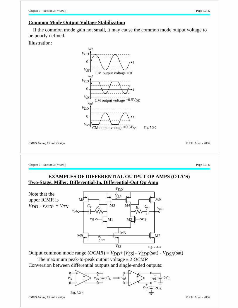
Common Mode Output Voltage Stabilization
If the common mode gain not small, it may cause the common mode output voltage to be poorly defined.
Illustration:
VDD
vod
t
Fig. 7.3-2
VSS
0
VDD
vod
t
VSS
0
VDD
vod
t
VSS
0
CM output voltage = 0
CM output voltage =0.5VDD
CM output voltage =0.5VSS
Chapter 7 – Section 3 (7/4/06)) Page 7.3-4.
CMOS Analog Circuit Design © P.E. Allen - 2006
EXAMPLES OF DIFFERENTIAL OUTPUT OP AMPS (OTA’S) Two-Stage, Miller, Differential-In, Differential-Out Op Amp
Note that the upper ICMR is VDD - VSGP + VTN Output common mode range (OCMR) = VDD+ |VSS| - VSDP(sat) - VDSN(sat) The maximum peak-to-peak output voltage 2·OCMR Conversion between differential outputs and single-ended outputs:
vod CL
+
-+-+
-vid
+
-vo1 2CL
+
-+-+
-vid
+
-
vo2+
-2CL
Fig. 7.3-4
vi1 M1 M2
M3 M4
M5
M6M8
VDD
VSS
VBN+-
Cc
M9
Cc
VBP+-
vi2
vo1vo2RzRz
M7
Fig. 7.3-3
Chapter 7 – Section 3 (7/4/06)) Page 7.3-5.
CMOS Analog Circuit Design © P.E. Allen - 2006
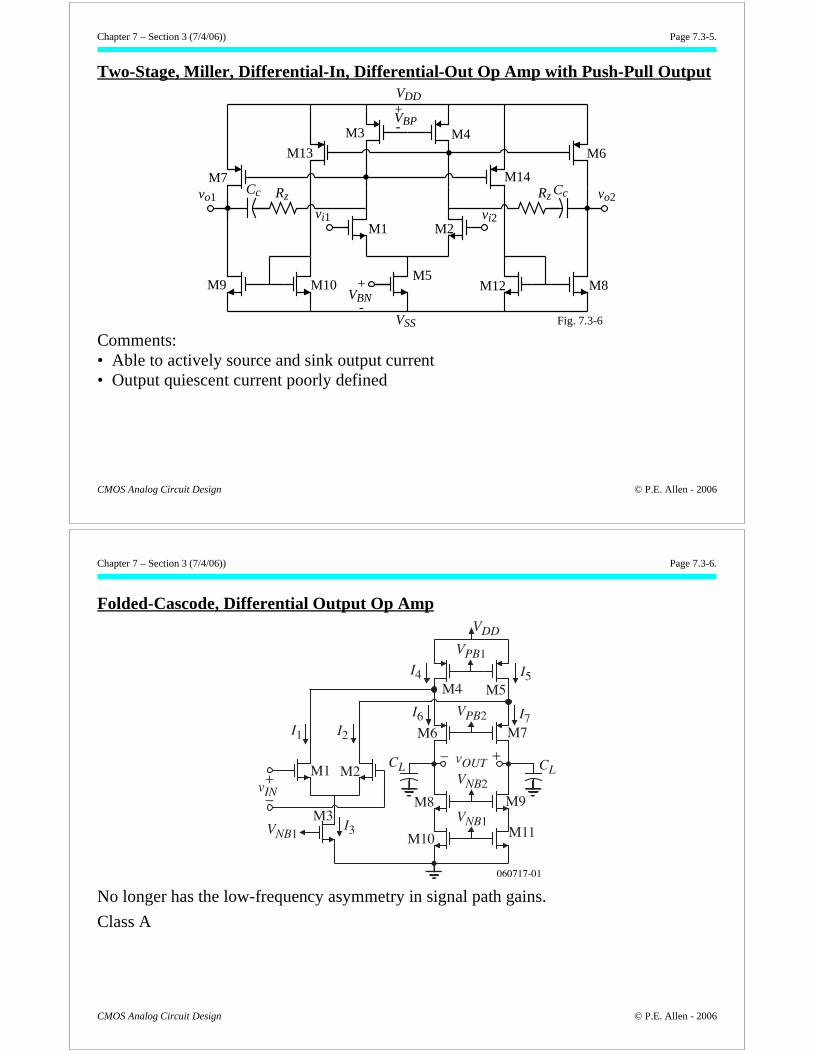
Two-Stage, Miller, Differential-In, Differential-Out Op Amp with Push-Pull Output
vi1M1 M2
M3 M4
M5
M6
M7
VDD
VSS
VBN+
-
Cc
M9
Cc
VBP+-
vi2
vo1 vo2RzRz
M8
Fig. 7.3-6
M10 M12
M13
M14
Comments: • Able to actively source and sink output current • Output quiescent current poorly defined
Chapter 7 – Section 3 (7/4/06)) Page 7.3-6.
CMOS Analog Circuit Design © P.E. Allen - 2006
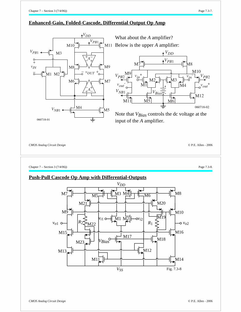
Folded-Cascode, Differential Output Op Amp
060717-01
VPB1
M4 M5
I6 VPB2
I4 I5
VDD
I7M6 M7
VNB2
M8 M9
M10 M11
+−
vIN
vOUT
VNB1
I1 I2
M1 M2
M3I3
CL
VNB1
+−CL
No longer has the low-frequency asymmetry in signal path gains.
Class A
Chapter 7 – Section 3 (7/4/06)) Page 7.3-7.
CMOS Analog Circuit Design © P.E. Allen - 2006
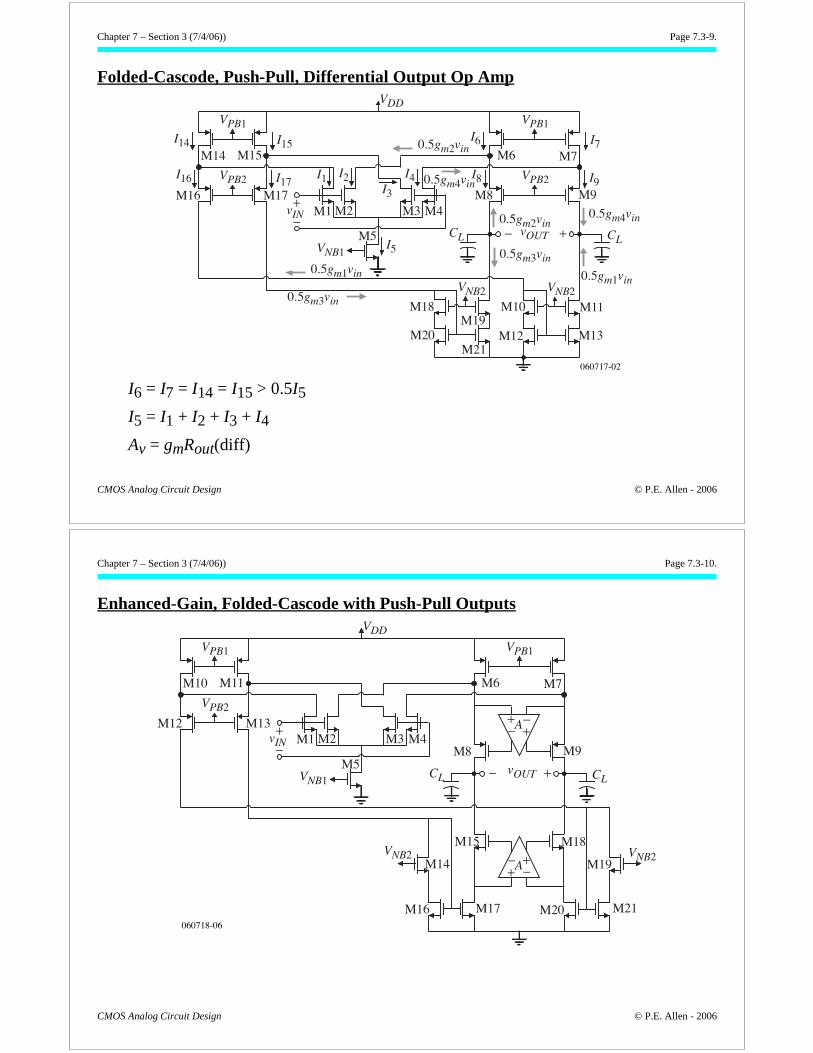
Enhanced-Gain, Folded-Cascode, Differential Output Op Amp
What about the A amplifier?
Below is the upper A amplifier:
060718-02
VDD
VPB1
VPB2 VPB2
VNB1 VBias
vin+ vin
-
vout+vout
- M1M2 M3
M4
M5 M6
M7 M8
M9 M10
M11M12
Note that VBias controls the dc voltage at the input of the A amplifier. 060718-01
vOUT
M4M5
M3
M7
M8 M9
M10 M11
M6
VDD
VPB1
+
−vIN
M1 M2
VNB1
A+− +
−
+− +
−A
+−
VPB1
Chapter 7 – Section 3 (7/4/06)) Page 7.3-8.
CMOS Analog Circuit Design © P.E. Allen - 2006
Push-Pull Cascode Op Amp with Differential-Outputs VDD
VSS
VBias
R2 M22
M23
R1
M19
M20
M1 M2
M3 M4M5 M6M7 M8
M9 M10
M11
M12M13
M14
M15 M16M17
M18
M21
vo1vi1 vi2
vo2
Fig. 7.3-8
Chapter 7 – Section 3 (7/4/06)) Page 7.3-9.
CMOS Analog Circuit Design © P.E. Allen - 2006
Folded-Cascode, Push-Pull, Differential Output Op Amp
060717-02
VPB1
M6 M7
I6
VPB2I4
I7
I9M8 M9
VNB2
M10 M11
M12 M13
+−
vIN
vOUTVNB1
I3
I2
M2 M3
M5I5
CL+−CL
I1
M1
VNB2
M18M19
M20M21
VPB1
M14 M15
I16 VPB2
I14 I15
VDD
I17M16 M17
M4
I8
0.5gm1vin
0.5gm3vin
0.5gm2vin
0.5gm4vin
0.5gm3vin
0.5gm4vin0.5gm2vin
0.5gm1vin
I6 = I7 = I14 = I15 > 0.5I5
I5 = I1 + I2 + I3 + I4
Av = gmRout(diff)
Chapter 7 – Section 3 (7/4/06)) Page 7.3-10.
CMOS Analog Circuit Design © P.E. Allen - 2006
Enhanced-Gain, Folded-Cascode with Push-Pull Outputs
060718-06
VPB1
M6 M7
M8 M9
M20
M19
M18
M21
+−
vIN
VNB1
M2 M3
M5CL+−CL
M1
VNB2M14
M17M16
M15
VPB1
M10 M11
VPB2
VDD
M12 M13M4
vOUT
A+− +
−
+− +
−AVNB2

Chapter 7 – Section 3 (7/4/06)) Page 7.3-11.
CMOS Analog Circuit Design © P.E. Allen - 2006
Cross-Coupled Differential Amplifier Stage
The cross-coupled input stage allows the push-pull output quiescent current to be well defined. Operation: Voltage loop vi1 - vi2 = -VGS1+ vGS1 + vSG4 - VSG4 = VSG3 - vSG3 - vGS2 + VGS2 Using the notation for ac, dc, and total variables gives, vi2 - vi1 = vid = (vsg1 + vgs4) = -(vsg3 + vgs2) If gm1 = gm2 = gm3 = gm4, then half of the differential input is applied across each transistor with the correct polarity.
i1 = gm1vid
2 = gm4vid
2 and i2 = -gm2vid
2 = -gm3vid
2
M1 M2
M3 M4
VGS2
VSG4
VGS1
VSG3
i1
i1i2
i2
vi1 vi2
Fig. 7.3-9
vGS1+
-
vSG4+
-vSG3
+
-
vGS2+
-
Chapter 7 – Section 3 (7/4/06)) Page 7.3-12.
CMOS Analog Circuit Design © P.E. Allen - 2006
Class AB, Differential Output Op Amp using a Cross-Coupled Differential Input Stage
M1 M2
M3 M4
M5 M6
M7
VDD
VSS
VBias+
-
R1
M24
M25
R2
M27
M28
M8M9 M10
M11 M12
M13
M14
M15
M16
M17 M18
M19 M20
M21 M22
M26
M23
vo2
vi2vi1
vo1
Fig. 7.3-10 Quiescent output currents are defined by the current in the input cross-coupled differential amplifier.
Chapter 7 – Section 3 (7/4/06)) Page 7.3-13.
CMOS Analog Circuit Design © P.E. Allen - 2006
COMMON MODE OUTPUT VOLTAGE STABILIZATION
Common Mode Feedback Circuits
Because the common mode gain is undefined, any common mode signal at the input can cause the output common mode voltage to be improperly defined. The common mode output voltage is stabilized by sensing the common mode output voltage and using negative feedback to adjust the common mode voltage to the desired value.
Model for the Output of Differential Output Op Amps: VDD
io1(source) Ro1
vo1
io1(sink) Ro3
io2(source)
io2(sink)
Ro2
Ro4
vo2
VDD
io1(source) Ro1
vo1
Io1(sink) Ro3
io2(source)
Io2(sink)
Ro2
Ro4
vo2
Class A Output Push-Pull Output 060718-08 Roi represents the self-resistance of the output sink/sources.
1.) If the common mode output voltage increases the sourcing current is too large.
2.) If the common mode output voltage decreases the sinking current is too large.
Chapter 7 – Section 3 (7/4/06)) Page 7.3-14.
CMOS Analog Circuit Design © P.E. Allen - 2006
Conceptual View of Common-Mode Feedback
060718-09
VDD
VCMREF
+
−
vo2vo1
OutputStageModel
Common ModeSensing Circuit
Function of the common-mode feedback circuit:
1.) If the common-mode output voltage increases, decrease the upper currents sources or increase the lower current sink until the common-mode voltage is equal to VCMREF.
2.) If the common-mode output voltage decreases, increase the upper currents sources or decrease the lower current sink until the common-mode voltage is equal to VCMREF.
Chapter 7 – Section 3 (7/4/06)) Page 7.3-15.
CMOS Analog Circuit Design © P.E. Allen - 2006
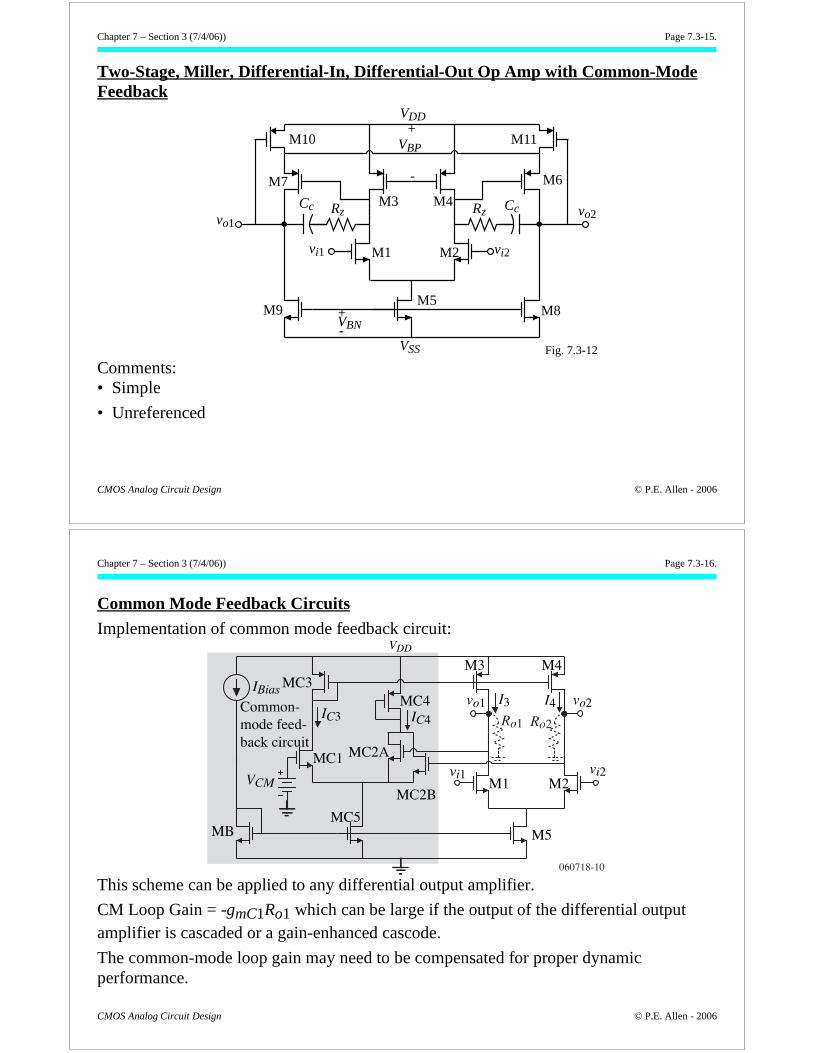
Two-Stage, Miller, Differential-In, Differential-Out Op Amp with Common-Mode Feedback
vi1 M1 M2
M3 M4
M5
M6M7
VDD
VSS
VBN+-
Cc
M9
Cc
VBP
+
-
vi2
vo1vo2RzRz
M8
Fig. 7.3-12
M10 M11
Comments: • Simple
• Unreferenced
Chapter 7 – Section 3 (7/4/06)) Page 7.3-16.
CMOS Analog Circuit Design © P.E. Allen - 2006
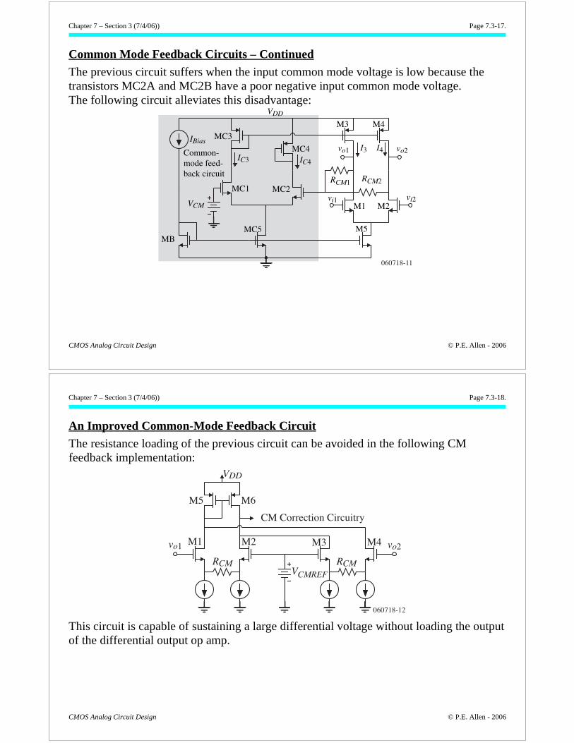
Common Mode Feedback Circuits
Implementation of common mode feedback circuit:
060718-10
vi1M1 M2
M3 M4
M5
VDD
IBias
VCM
vo1
MC2A
MC2B
MC1
MC3MC4
MC5MB
I3 I4IC4IC3
Common-mode feed-back circuit
Ro1 Ro2
vi2
vo2
This scheme can be applied to any differential output amplifier.
CM Loop Gain = -gmC1Ro1 which can be large if the output of the differential output amplifier is cascaded or a gain-enhanced cascode.
The common-mode loop gain may need to be compensated for proper dynamic performance.
Chapter 7 – Section 3 (7/4/06)) Page 7.3-17.
CMOS Analog Circuit Design © P.E. Allen - 2006
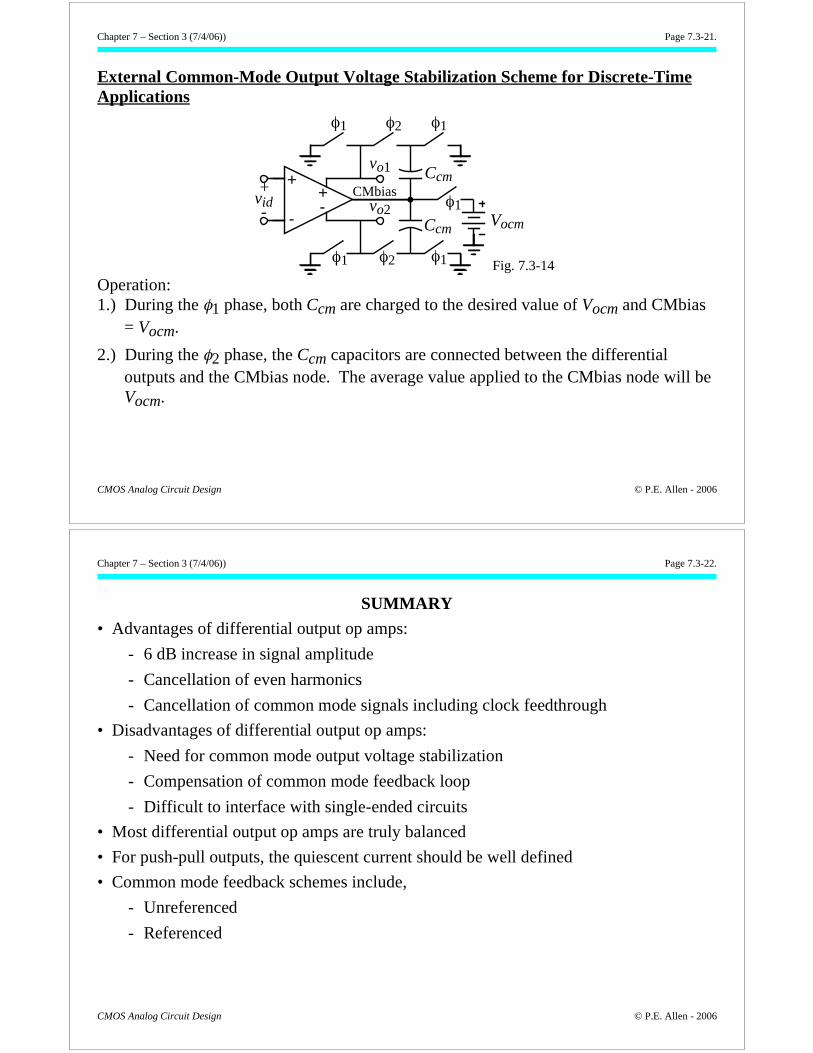
Common Mode Feedback Circuits – Continued
The previous circuit suffers when the input common mode voltage is low because the transistors MC2A and MC2B have a poor negative input common mode voltage. The following circuit alleviates this disadvantage:
060718-11
vi1M1 M2
M3 M4
M5
VDD
IBias
VCM
vo2vo1
vi2MC2MC1
MC3
MC4
MC5MB
I3 I4
IC4IC3Common-mode feed-back circuit
RCM1 RCM2
Chapter 7 – Section 3 (7/4/06)) Page 7.3-18.
CMOS Analog Circuit Design © P.E. Allen - 2006
An Improved Common-Mode Feedback Circuit
The resistance loading of the previous circuit can be avoided in the following CM feedback implementation:
VDD
060718-12
VCMREF
RCM RCM
vo1 vo2
CM Correction Circuitry
M1 M2 M3 M4
M5 M6
This circuit is capable of sustaining a large differential voltage without loading the output of the differential output op amp.

Chapter 7 – Section 3 (7/4/06)) Page 7.3-19.
CMOS Analog Circuit Design © P.E. Allen - 2006
Frequency Response of the CM Feedback Circuit
Consider the following CM feedback circuit implementation:
060718-13
VPB1
M4 M5
VPB2
VDD
M6 M7
VNB2M8
M10M11
+−
vIN
vOUT
VNB1
M1 M2
M3VCMREF
+−
M9
M12
M13 M14
M15 M16
The CM feedback path has two poles – one at the gates of M10 and M11 and the dominant output pole of the differential output op amp.
Chapter 7 – Section 3 (7/4/06)) Page 7.3-20.
CMOS Analog Circuit Design © P.E. Allen - 2006
Improved CM Feedback Frequency Response
The circuit on the previous page can be modified to eliminate the pole at the gates of M10 and M11 as follows:
060718-14
VPB1
M4 M5
VPB2
VDD
M6 M7
VNB2M8
M10 M11
+−
vin
vo1
VNB1
M1 M2
M3
VCMREF
M9
M12
M13 M14
M16M15
VNB1
VNB2
M17
M18M19
vo2
Chapter 7 – Section 3 (7/4/06)) Page 7.3-21.
CMOS Analog Circuit Design © P.E. Allen - 2006
External Common-Mode Output Voltage Stabilization Scheme for Discrete-Time Applications
Ccm+
-+-+
-vid
vo1
vo2CMbias
φ1 φ2
Ccm Vocm
φ1 φ2
φ1
φ1
φ1 Fig. 7.3-14 Operation: 1.) During the 1 phase, both Ccm are charged to the desired value of Vocm and CMbias
= Vocm.
2.) During the 2 phase, the Ccm capacitors are connected between the differential outputs and the CMbias node. The average value applied to the CMbias node will be Vocm.
Chapter 7 – Section 3 (7/4/06)) Page 7.3-22.
CMOS Analog Circuit Design © P.E. Allen - 2006
SUMMARY
• Advantages of differential output op amps:
- 6 dB increase in signal amplitude
- Cancellation of even harmonics
- Cancellation of common mode signals including clock feedthrough
• Disadvantages of differential output op amps:
- Need for common mode output voltage stabilization
- Compensation of common mode feedback loop
- Difficult to interface with single-ended circuits
• Most differential output op amps are truly balanced
• For push-pull outputs, the quiescent current should be well defined
• Common mode feedback schemes include,
- Unreferenced
- Referenced
Chapter 7 – Section 4 (7/4/06)) Page 7.4-1.
CMOS Analog Circuit Design © P.E. Allen - 2006
SECTION 7.4 – LOW POWER OP AMPS Objective
The objective of this presentation is:
1.) Examine op amps that have minimum static power
- Minimize power dissipation
- Work at low values of power supply
- Tradeoff speed for less power
Outline
• Weak inversion • Methods of creating an overdrive • Examples • Summary
Chapter 7 – Section 4 (7/4/06)) Page 7.4-2.
CMOS Analog Circuit Design © P.E. Allen - 2006
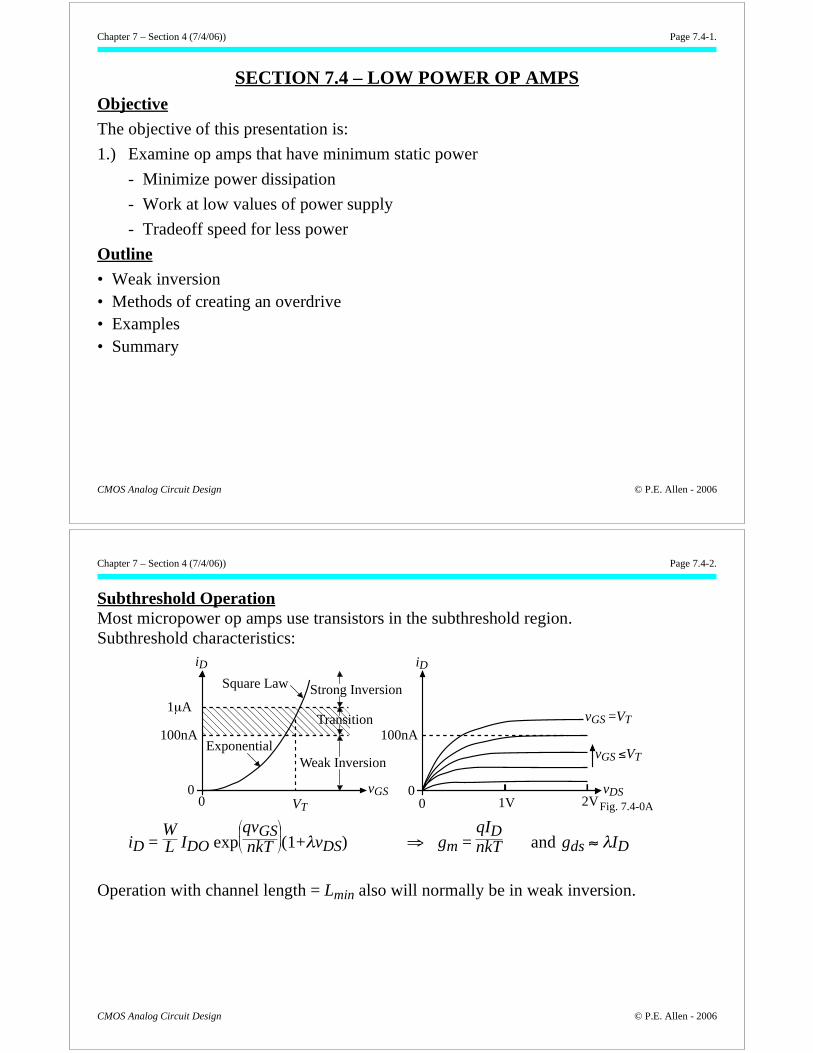
Subthreshold Operation Most micropower op amps use transistors in the subthreshold region. Subthreshold characteristics:
�����100nA
1μA
Weak Inversion
Transition
Strong InversionSquare Law
Exponential
iD
vGS
iD
vDSVT
100nAvGS =VT
vGS ≤VT
Fig. 7.4-0A1V 2V000
0
iD = WL IDO exp
qvGSnkT (1+ vDS) gm =
qIDnkT and gds ID
Operation with channel length = Lmin also will normally be in weak inversion.

Chapter 7 – Section 4 (7/4/06)) Page 7.4-3.
CMOS Analog Circuit Design © P.E. Allen - 2006
Two-Stage, Miller Op Amp Operating in Weak Inversion
-
+vin
M1 M2
M3 M4
M5
M6
M7
vout
VDD
VSS
VBias+
-
Cc
CL
Fig.7.4-1 Low frequency response:
Avo = gm2gm6 ro2ro4
ro2 + ro4
ro6ro7ro6 + ro7
= 1
n2n6(kT/q)2( 2 + 4)( 6 + 7) (No longer 1ID
)
GB and SR:
GB = ID1
(n1kT/q)C and SR = ID5C = 2
ID1C = 2GB n1
kTq = 2GBn1Vt
Chapter 7 – Section 4 (7/4/06)) Page 7.4-4.
CMOS Analog Circuit Design © P.E. Allen - 2006
Example 7.4-1 Gain and GB Calculations for Subthreshold Op Amp.
Calculate the gain, GB, and SR of the op amp shown above. The currents are ID5 = 200 nA and ID7 = 500 nA. The device lengths are 1 μm. Values for n are 1.5 and 2.5 for p-channel and n-channel transistors respectively. The compensation capacitor is 5 pF. Use Table 3.1-2 as required. Assume that the temperature is 27 °C. If VDD = 1.5V and VSS = -1.5V, what is the power dissipation of this op amp?
Solution The low-frequency small-signal gain is,
Av = 1
(1.5)(2.5)(0.026)2(0.04 + 0.05)(0.04 + 0.05) = 43,701 V/V
The gain bandwidth is
GB = 100x10-9
2.5(0.026)(5x10-12) = 307,690 rps 49.0 kHz
The slew rate is SR = (2)(307690)(2.5)(0.026) = 0.04 V/μs The power dissipation is, Pdiss = 3(0.7μA) =2.1μW
Chapter 7 – Section 4 (7/4/06)) Page 7.4-5.
CMOS Analog Circuit Design © P.E. Allen - 2006
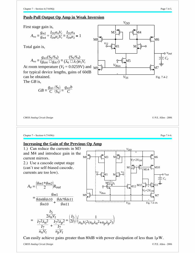
Push-Pull Output Op Amp in Weak Inversion
First stage gain is,
Avo = gm2gm4
= ID2n4VtID4n2Vt
= ID2n4ID4n2
1
Total gain is,
Avo = gm1(S6/S4)
(gds6 + gds7) = (S6/S4)
( 6 + 7)n1Vt
At room temperature (Vt = 0.0259V) and for typical device lengths, gains of 60dB can be obtained. The GB is,
GB = gm1C
S6S4
= gm1b
C
vout
VDD
VSS
VBias+
-
Cc
M1 M2
M3 M4
M5
M6
M7
M8
M9
vi2
Fig. 7.4-2
Chapter 7 – Section 4 (7/4/06)) Page 7.4-6.
CMOS Analog Circuit Design © P.E. Allen - 2006
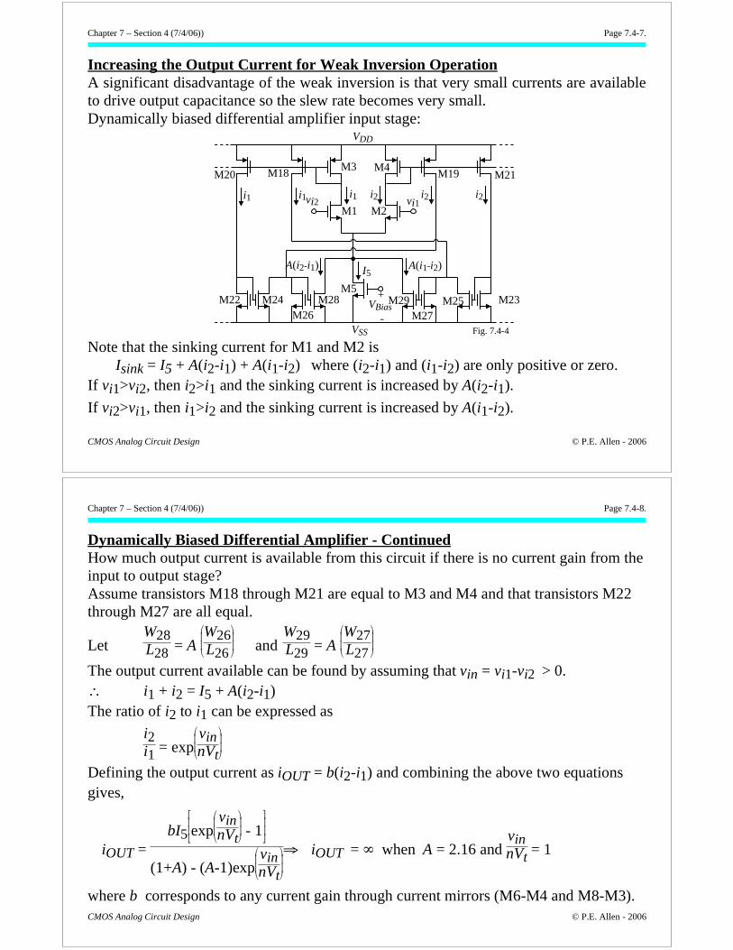
Increasing the Gain of the Previous Op Amp 1.) Can reduce the currents in M3 and M4 and introduce gain in the current mirrors. 2.) Use a cascode output stage (can’t use self-biased cascode, currents are too low).
Av = gm1+gm2
2 Rout
= gm1
gds6gds10gm10
+ gds7gds11
gm11
=
I52nnVt
I72 n2
I7nnVt
+ I72 p2
I7npVt
= I5
2I7 1
nnVt2(nn n2+np p2)
Can easily achieve gains greater than 80dB with power dissipation of less than 1μW.
M6
M7
vout
VDD
VSS
VBias
+
-
Cc
M1 M2
M3 M4
M5
M8
M9
vi2
M10
M11M12
M13M14
M15
vi1
I5
+
-
VT+2VON
+
-
VT+2VON
Fig. 7.4-3A
Chapter 7 – Section 4 (7/4/06)) Page 7.4-7.
CMOS Analog Circuit Design © P.E. Allen - 2006
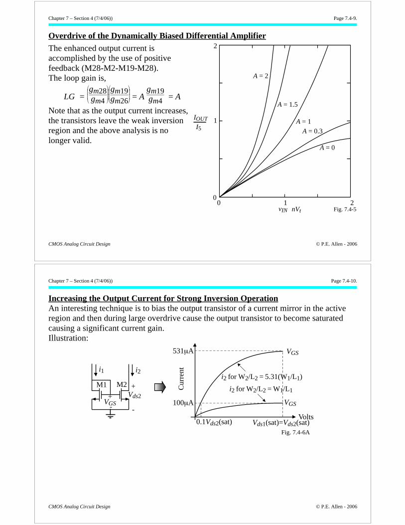
Increasing the Output Current for Weak Inversion Operation A significant disadvantage of the weak inversion is that very small currents are available to drive output capacitance so the slew rate becomes very small. Dynamically biased differential amplifier input stage:
VDD
VSS
VBias+
-
vi2 vi1M2M1
M3 M4
M5
I5
M18 M19M20 M21
M22 M23M24 M25M26 M27
M28 M29
i1 i2 i2 i2i1i1
A(i2-i1) A(i1-i2)
Fig. 7.4-4 Note that the sinking current for M1 and M2 is Isink = I5 + A(i2-i1) + A(i1-i2) where (i2-i1) and (i1-i2) are only positive or zero. If vi1>vi2, then i2>i1 and the sinking current is increased by A(i2-i1).
If vi2>vi1, then i1>i2 and the sinking current is increased by A(i1-i2).
Chapter 7 – Section 4 (7/4/06)) Page 7.4-8.
CMOS Analog Circuit Design © P.E. Allen - 2006
Dynamically Biased Differential Amplifier - Continued How much output current is available from this circuit if there is no current gain from the input to output stage? Assume transistors M18 through M21 are equal to M3 and M4 and that transistors M22 through M27 are all equal.
Let W28L28
= A W26L26
and W29L29
= A W27L27
The output current available can be found by assuming that vin = vi1-vi2 > 0. i1 + i2 = I5 + A(i2-i1)
The ratio of i2 to i1 can be expressed as
i2i1 = exp
vinnVt
Defining the output current as iOUT = b(i2-i1) and combining the above two equations gives,
iOUT = bI5 exp
vinnVt
- 1
(1+A) - (A-1)expvinnVt
iOUT = when A = 2.16 and vinnVt
= 1
where b corresponds to any current gain through current mirrors (M6-M4 and M8-M3).
Chapter 7 – Section 4 (7/4/06)) Page 7.4-9.
CMOS Analog Circuit Design © P.E. Allen - 2006
Overdrive of the Dynamically Biased Differential Amplifier
The enhanced output current is accomplished by the use of positive feedback (M28-M2-M19-M28). The loop gain is,
LG = gm28gm4
gm19gm26
= A gm19gm4
= A
Note that as the output current increases, the transistors leave the weak inversion region and the above analysis is no longer valid.
A = 0
A = 0.3A = 1
A = 1.5
A = 2
IOUT
I5
2
1
00 1 2
vIN nVt Fig. 7.4-5
Chapter 7 – Section 4 (7/4/06)) Page 7.4-10.
CMOS Analog Circuit Design © P.E. Allen - 2006
Increasing the Output Current for Strong Inversion Operation An interesting technique is to bias the output transistor of a current mirror in the active region and then during large overdrive cause the output transistor to become saturated causing a significant current gain. Illustration:
+Vds2
-
i1 i2
M1 M2
Fig. 7.4-6A
Vds1(sat)=Vds2(sat)0.1Vds2(sat)
100μA
531μA
i2 for W2/L2 = 5.31(W1/L1)
Volts
Cur
rent
i2 for W2/L2 = W1/L1+
VGS-
VGS
VGS
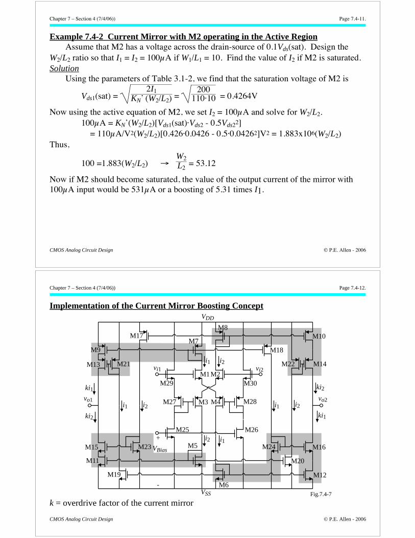
Chapter 7 – Section 4 (7/4/06)) Page 7.4-11.
CMOS Analog Circuit Design © P.E. Allen - 2006
Example 7.4-2 Current Mirror with M2 operating in the Active Region Assume that M2 has a voltage across the drain-source of 0.1Vds(sat). Design the W2/L2 ratio so that I1 = I2 = 100μA if W1/L1 = 10. Find the value of I2 if M2 is saturated. Solution Using the parameters of Table 3.1-2, we find that the saturation voltage of M2 is
Vds1(sat) = 2I1
KN’ (W2/L2) = 200
110·10 = 0.4264V
Now using the active equation of M2, we set I2 = 100μA and solve for W2/L2. 100μA = KN’(W2/L2)[Vds1(sat)·Vds2 - 0.5Vds22] = 110μA/V2(W2/L2)[0.426·0.0426 - 0.5·0.04262]V2 = 1.883x10⁶(W2/L2) Thus,
100 =1.883(W2/L2) W2L2
= 53.12
Now if M2 should become saturated, the value of the output current of the mirror with 100μA input would be 531μA or a boosting of 5.31 times I1.
Chapter 7 – Section 4 (7/4/06)) Page 7.4-12.
CMOS Analog Circuit Design © P.E. Allen - 2006
Implementation of the Current Mirror Boosting Concept VDD
VSS
i1
i1
i2
i2
i2 i2i1 i1
ki2 ki1
ki1
M8
M7
M5
M6
M10
M14
M16
M12
M11
M15
M13
M9
M17
M18
M19
M20
M21 M22
M23 M24
vo2vo1
Fig.7.4-7
M1 M2
M3 M4
VBias
+
-
M25 M26
M27 M28
M29 M30
vi2vi1
ki2
k = overdrive factor of the current mirror
Chapter 7 – Section 4 (7/4/06)) Page 7.4-13.
CMOS Analog Circuit Design © P.E. Allen - 2006
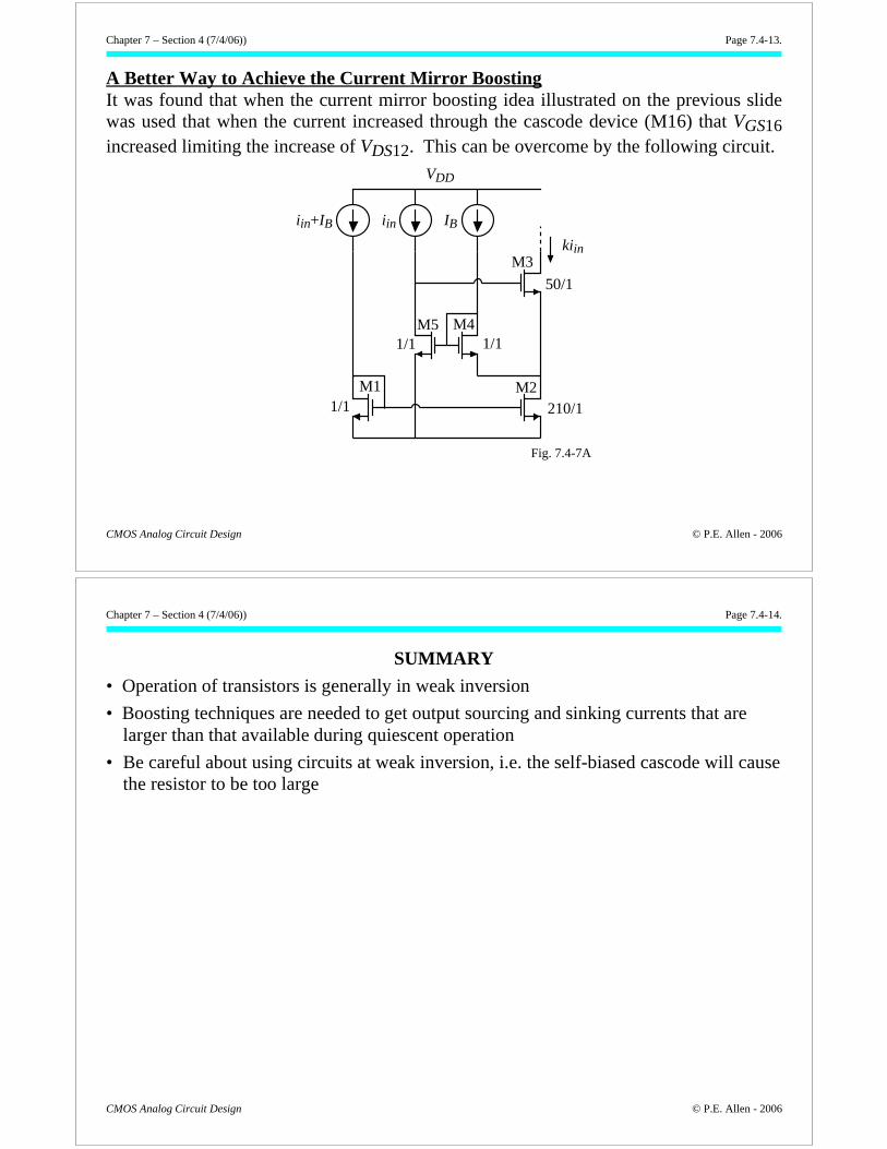
A Better Way to Achieve the Current Mirror Boosting It was found that when the current mirror boosting idea illustrated on the previous slide was used that when the current increased through the cascode device (M16) that VGS16 increased limiting the increase of VDS12. This can be overcome by the following circuit.
M1 M2
M3
M4M5
VDD
iin+IB iin
kiin
IB
1/1
1/1 1/1
50/1
210/1
Fig. 7.4-7A
Chapter 7 – Section 4 (7/4/06)) Page 7.4-14.
CMOS Analog Circuit Design © P.E. Allen - 2006
SUMMARY
• Operation of transistors is generally in weak inversion
• Boosting techniques are needed to get output sourcing and sinking currents that are larger than that available during quiescent operation
• Be careful about using circuits at weak inversion, i.e. the self-biased cascode will cause the resistor to be too large
Chapter 7 – Section 5 (7/4/06)) Page 7.5-1.
CMOS Analog Circuit Design © P.E. Allen - 2006
SECTION 7.5 – LOW NOISE OP AMPS Objective
The objective of this presentation is:
1.) Review the principles of low noise design
2.) Show how to reduce the noise of op amps
Outline
• Review of noise analysis
• Low noise op amps
• Low noise op amps using lateral BJTs
• Low noise op amps using doubly correlated sampling
• Summary
Chapter 7 – Section 5 (7/4/06)) Page 7.5-2.
CMOS Analog Circuit Design © P.E. Allen - 2006
Introduction Why do we need low noise op amps? Dynamic range: Signal-to-noise ratio (SNR)
= Maximum RMS Signal
Noise
(SNDR includes both noise and distortion) Consider a 14 bit digital-to-analog converter with a 1V reference with a bandwidth of 1MHz.
Maximum RMS signal is 0.5V
2 = 0.3535 Vrms
A 14 bit D/A converter requires 14x6dB dynamic range or 84 dB or 16,400.
The value of the least significant bit (LSB) = 0.3535
16,400 = 21.6μVrms
If the equivalent input noise of the op amp is not less than this value, then the LSB cannot be resolved and the D/A converter will be in error. An op amp with an equivalent input-noise spectral density of 10nV/ Hz will have an rms noise voltage of approximately (10nV/ Hz)(1000 Hz) = 10μVrms in a 1MHz bandwidth.
����
����VDD
Noise + Distortion
Dynamic Range = 6dBx(Number. of bits)
Fig. 7.5-0B
Chapter 7 – Section 5 (7/4/06)) Page 7.5-3.
CMOS Analog Circuit Design © P.E. Allen - 2006
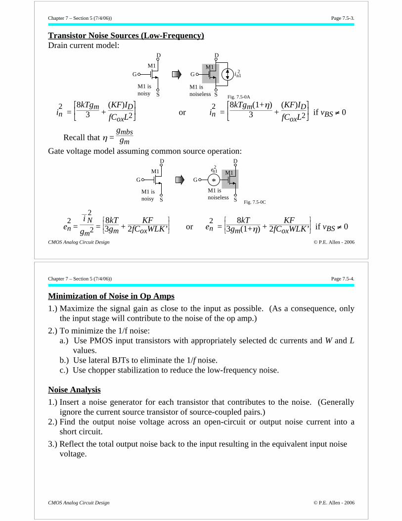
Transistor Noise Sources (Low-Frequency) Drain current model:
i 2n1
D
G
S
D
G
S
M1 M1
M1 isnoiseless
M1 isnoisy
Fig. 7.5-0A
i2n =
8kTgm3 +
(KF)IDfCoxL2 or i
2n =
8kTgm(1+ )3 +
(KF)IDfCoxL2 if vBS 0
Recall that = gmbsgm
Gate voltage model assuming common source operation: D
G
S
D
G
S
M1 M1
M1 isnoiseless
M1 isnoisy
Fig. 7.5-0C
e2n1
*
e2n =
i2N
gm2 = 8kT3gm
+ KF
2fCoxWLK’ or e2n =
8kT3gm(1+ ) +
KF2fCoxWLK’ if vBS 0
Chapter 7 – Section 5 (7/4/06)) Page 7.5-4.
CMOS Analog Circuit Design © P.E. Allen - 2006
Minimization of Noise in Op Amps
1.) Maximize the signal gain as close to the input as possible. (As a consequence, only the input stage will contribute to the noise of the op amp.)
2.) To minimize the 1/f noise: a.) Use PMOS input transistors with appropriately selected dc currents and W and L
values. b.) Use lateral BJTs to eliminate the 1/f noise. c.) Use chopper stabilization to reduce the low-frequency noise. Noise Analysis
1.) Insert a noise generator for each transistor that contributes to the noise. (Generally ignore the current source transistor of source-coupled pairs.)
2.) Find the output noise voltage across an open-circuit or output noise current into a short circuit.
3.) Reflect the total output noise back to the input resulting in the equivalent input noise voltage.
Chapter 7 – Section 5 (7/4/06)) Page 7.5-5.
CMOS Analog Circuit Design © P.E. Allen - 2006
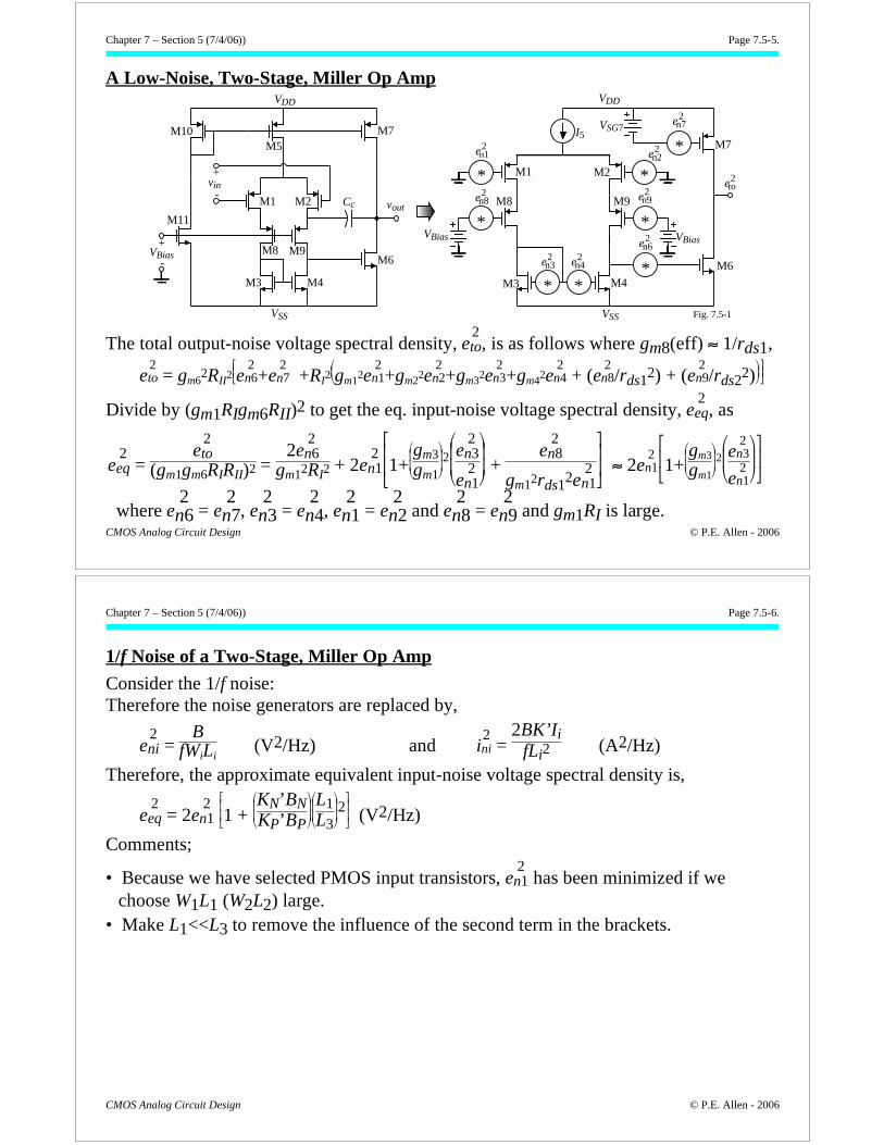
A Low-Noise, Two-Stage, Miller Op Amp
M3 M4
M6
vout
VDD
VSS
VBias
Cc
+
-
vin+
-M1 M2
M8 M9
M7M5
M10
M11
Fig. 7.5-1
VDD
VSS
e2n3 e2
n4
VBias VBias
M1 M2
M3 M4
M8 M9
e2n2
e2n1
e2n6
e2n7
I5M7
M6
e2to
VSG7
*
*
*
*
* *
e2n8
*
e2n9
*
The total output-noise voltage spectral density, e2to, is as follows where gm8(eff) 1/rds1,
e2to = gm6
2RII2 e2
n6+e2n7 +RI2 gm12e
2n1+gm22e
2n2+gm32e
2n3+gm42e
2n4 + (e
2n8/rds12) + (e
2n9/rds22)
Divide by (gm1RIgm6RII)2 to get the eq. input-noise voltage spectral density, e2eq, as
e2eq =
e2to
(gm1gm6RIRII)2 = 2e
2n6
gm12RI2 + 2e
2n1 1+
gm3gm1
2 e2
n3
e2
n1 +
e2n8
gm12rds12e2n1
2e2n1 1+
gm3
gm1
2 e2
n3
e2
n1
where e2
n6 = e2
n7, e2
n3 = e2
n4, e2
n1 = e2
n2 and e2
n8 = e2
n9 and gm1RI is large.
Chapter 7 – Section 5 (7/4/06)) Page 7.5-6.
CMOS Analog Circuit Design © P.E. Allen - 2006
1/f Noise of a Two-Stage, Miller Op Amp
Consider the 1/f noise: Therefore the noise generators are replaced by,
e2ni =
BfWiLi
(V2/Hz) and i2ni =
2BK’IifLi2 (A2/Hz)
Therefore, the approximate equivalent input-noise voltage spectral density is,
e2eq = 2e
2n1 1 +
KN’BNKP’BP
L1L3
2 (V2/Hz)
Comments;
• Because we have selected PMOS input transistors, e2
n1 has been minimized if we choose W1L1 (W2L2) large.
• Make L1<<L3 to remove the influence of the second term in the brackets.
Chapter 7 – Section 5 (7/4/06)) Page 7.5-7.
CMOS Analog Circuit Design © P.E. Allen - 2006
Thermal Noise of a Two-Stage, Miller Op Amp
Let us focus next on the thermal noise: The noise generators are replaced by,
e2ni
8kT3gm (V2/Hz) and i
2ni
8kTgm3 (A2/Hz)
where the influence of the bulk has been ignored. The approximate equivalent input-noise voltage spectral density is,
e2eq = 2e
2n1 1+
gm3gm1
2 e2
n3
e2
n1 = 2e
2n1 1 +
KNW3L1KPW1L3 (V2/Hz)
Comments: • The choices that reduce the 1/f noise also reduce the thermal noise. Noise Corner: Equating the equivalent input-noise voltage spectral density for the 1/f noise and the thermal noise gives the noise corner, fc, as
fc = 3gmB
8kTWL
Chapter 7 – Section 5 (7/4/06)) Page 7.5-8.
CMOS Analog Circuit Design © P.E. Allen - 2006
Example 7.5-1 Design of A Two-Stage, Miller Op Amp for Low 1/f Noise Use the parameters of Table 3.1-2 along with the value of KF = 4x10-28 F·A for NMOS and 0.5x10⁻²⁸ F·A for PMOS and design the previous op amp to minimize the 1/f noise. Calculate the corresponding thermal noise and solve for the noise corner frequency. From this information, estimate the rms noise in a frequency range of 1Hz to 100kHz. What is the dynamic range of this op amp if the maximum signal is a 1V peak-to-peak sinusoid? Solution 1.) The 1/f noise constants, BN and BP are calculated as follows.
BN = KF
2CoxKN’ = 4x10-28F·A
2·24.7x10-4F/m2·110x10-6A2/V = 7.36x10⁻²² (V·m)2
and
BP = KF
2CoxKP’ = 0.5x10⁻²⁸F·A
2·24.7x10-4F/m2·50x10-6A2/V = 2.02x10⁻²² (V·m)2
2.) Now select the geometry of the various transistors that influence the noise performance.
To keep e2
n1 small, let W1 = 100μm and L1 = 1μm. Select W3 = 100μm and L3 = 20μm and letW8 and L8 be the same as W1 and L1 since they little influence on the noise.

Chapter 7 – Section 5 (7/4/06)) Page 7.5-9.
CMOS Analog Circuit Design © P.E. Allen - 2006
Example 7.5-1 - Continued Of course, M1 is matched with M2, M3 with M4, and M8 with M9.
e2
n1 = BP
fW1L1 = 2.02x10-22
f·100μm·1μm = 2.02x10⁻¹²
f (V2/Hz)
e2eq = 2x
2.02x10-12
f 1 + 110·7.3650·2.02
2 120
2 = 4.04x10⁻¹²
f 1.1606 = 4.689x10⁻¹²
f (V2/Hz)
Note at 100Hz, the voltage noise in a 1Hz band is 4.7x10⁻¹⁴V2(rms) or 0.216μV(rms). 3.) The thermal noise at room temperature is
e2
n1 = 8kT3gm =
8·1.38x10-23·3003·707x10-6 = 1.562x10⁻¹⁷ (V2/Hz)
which gives
e2eq = 2·1.562x10-17 1 +
110·100·150·100·20 = 3.124x10-17·1.33= 4.164x10⁻¹⁷ (V2/Hz)
4.) The noise corner frequency is found by equating the two expressions for e2eq to get
fc = 4.689x10⁻¹²
4.164x10-17 = 112.6kHz
This noise corner is indicative of the fact that the thermal noise is much less than the 1/f noise.
Chapter 7 – Section 5 (7/4/06)) Page 7.5-10.
CMOS Analog Circuit Design © P.E. Allen - 2006
Example 7.5-1 - Continued 5.) To estimate the rms noise in the bandwidth from 1Hz to 100,000Hz, we will ignore the thermal noise and consider only the 1/f noise. Performing the integration gives
Veq(rms)2 = 1
105
4.689x10⁻¹²
f df = 4.689x10⁻¹²[ln(100,000) - ln(1)]
= 0.540x10⁻¹⁰ Vrms2 = 7.34 μVrms
The maximum signal in rms is 0.353V. Dividing this by 7.34μV gives 48,044 or 93.6dB which is equivalent to about 15 bits of resolution. 6.) Note that the design of the remainder of the op amp will have little influence on the noise and is not included in this example.
Chapter 7 – Section 5 (7/4/06)) Page 7.5-11.
CMOS Analog Circuit Design © P.E. Allen - 2006
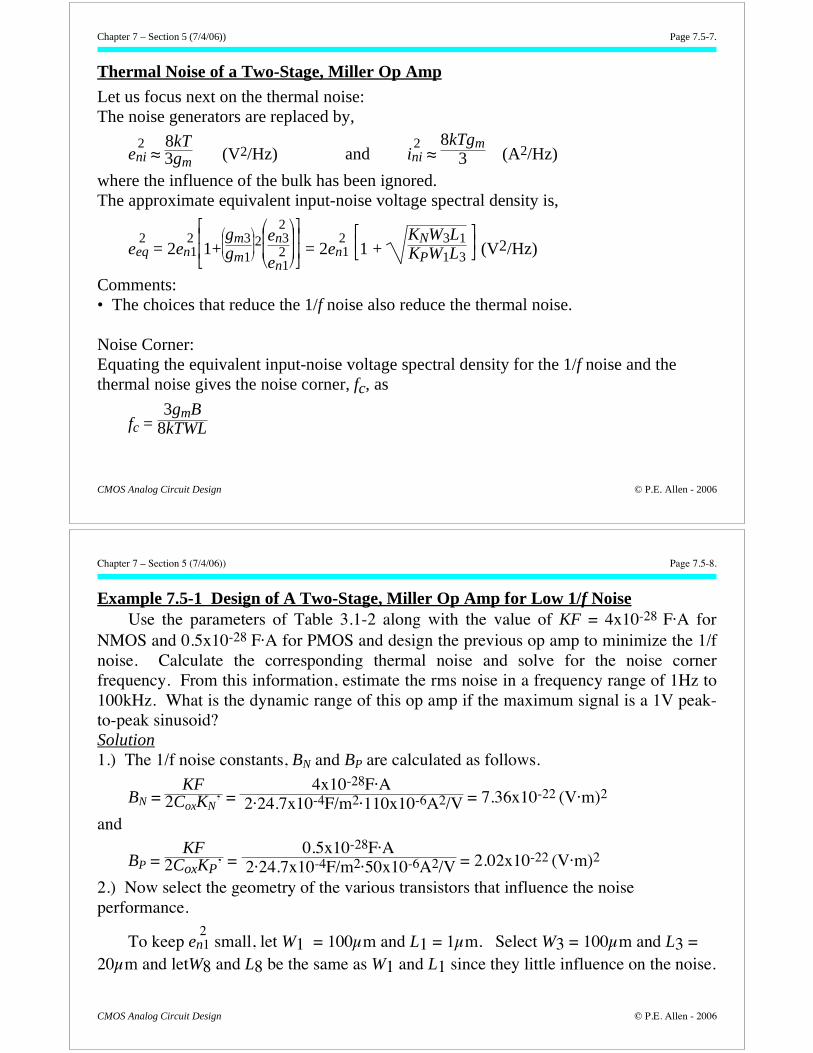
Lateral BJT
Since the 1/f noise is associated with current flowing at the surface of the channel, the lateral BJT offers a lower 1/f noise input device because the majority of current flows beneath the surface.
��������n+ p+ n+ n+n+
p-well
n-substrate
Base EmitterVertical Collector (VDD)
Base
Emitter
LateralCollector
LateralCollector
VerticalCollector
(VDD)
Cross-section of a NPN lateral BJT. Symbol. Fig. 7.5-3 Comments: • Base of the BJT is the well • Two collectors-one horizontal (desired) and one vertical (undesired)
• Collector efficiency is defined as Lateral collector currentTotal collector current and is 60-70%
• Reverse biased collector-base acts like a photodetector and is often used for light-sensing purposes
• A triple well process allows the vertical collector current to avoid the substrate.
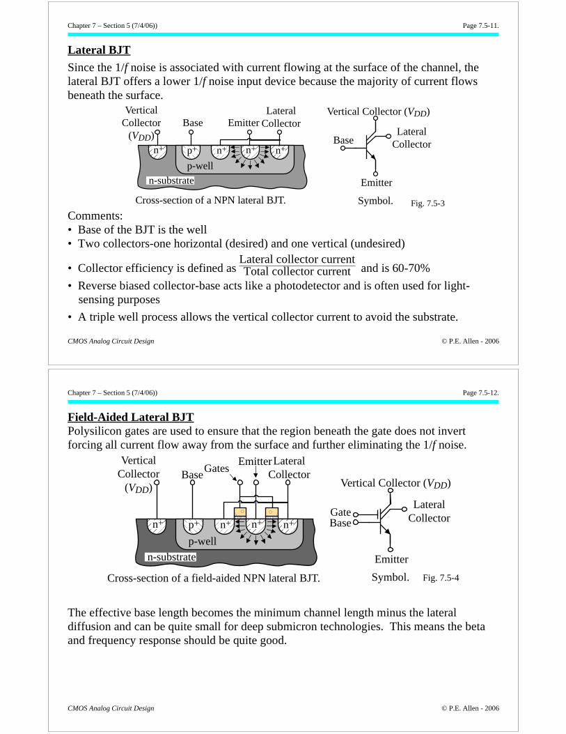
Chapter 7 – Section 5 (7/4/06)) Page 7.5-12.
CMOS Analog Circuit Design © P.E. Allen - 2006
Field-Aided Lateral BJT Polysilicon gates are used to ensure that the region beneath the gate does not invert forcing all current flow away from the surface and further eliminating the 1/f noise.
��������n+ p+ n+ n+n+
p-well
n-substrate
BaseEmitter
Vertical Collector (VDD)
Base
Emitter
LateralCollector
LateralCollector
VerticalCollector
(VDD)
Cross-section of a field-aided NPN lateral BJT. Symbol. Fig. 7.5-4����
Gates
Gate
The effective base length becomes the minimum channel length minus the lateral diffusion and can be quite small for deep submicron technologies. This means the beta and frequency response should be quite good.
Chapter 7 – Section 5 (7/4/06)) Page 7.5-13.
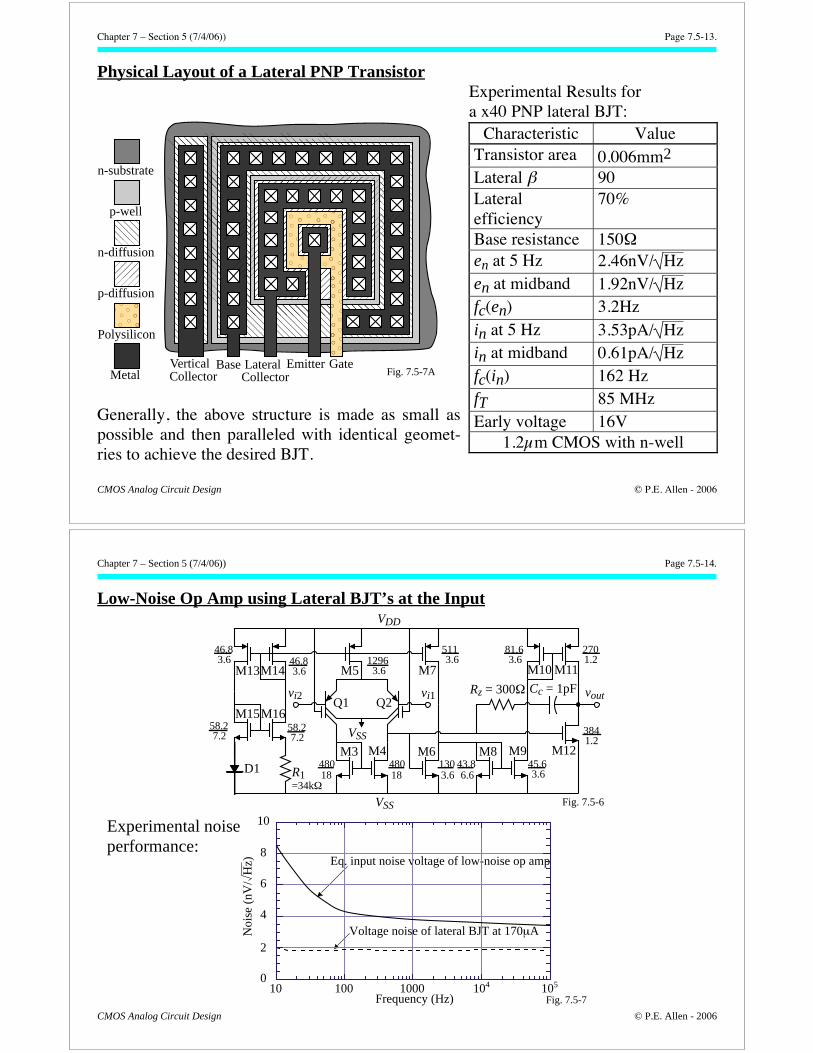
CMOS Analog Circuit Design © P.E. Allen - 2006
Physical Layout of a Lateral PNP Transistor Experimental Results for a x40 PNP lateral BJT:
������������
������������������������������������
Base Lateral Emitter GateVerticalCollectorCollector
n-substrate
��
n-diffusion
��
p-diffusion
��Polysilicon
Metal
p-well
Fig. 7.5-7A
����������������
������������
Generally, the above structure is made as small as possible and then paralleled with identical geomet-ries to achieve the desired BJT.
Characteristic Value Transistor area 0.006mm2 Lateral 90 Lateral efficiency
70%
Base resistance 150 en at 5 Hz 2.46nV/ Hz en at midband 1.92nV/ Hz fc(en) 3.2Hz in at 5 Hz 3.53pA/ Hz in at midband 0.61pA/ Hz fc(in) 162 Hz fT 85 MHz Early voltage 16V
1.2μm CMOS with n-well
Chapter 7 – Section 5 (7/4/06)) Page 7.5-14.
CMOS Analog Circuit Design © P.E. Allen - 2006
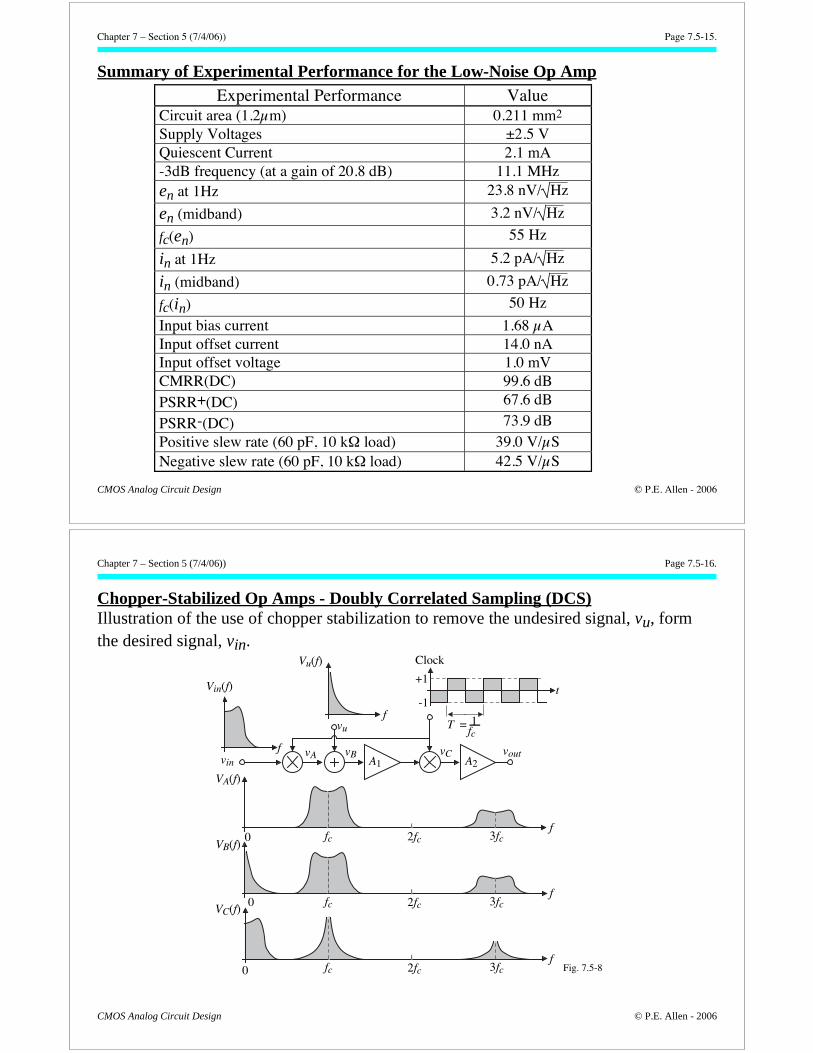
Low-Noise Op Amp using Lateral BJT’s at the Input
vout
VDD
VSS
Cc = 1pF
VSS
Q1 Q2
M3 M4
M5
M6
M7
M8 M9
M10 M11
M12
M13M14
M15M16
R1=34kΩ
D1
Rz = 300Ω
48018
48018
1303.6
43.86.6
45.63.6
81.63.6
5113.61296
3.6
3841.2
2701.246.8
3.6
46.83.6
58.27.2
58.27.2
vi1vi2
Fig. 7.5-6
0
2
4
6
8
10
10 100 1000 104 105
Frequency (Hz)
Noi
se (
nV/
Hz) Eq. input noise voltage of low-noise op amp
Voltage noise of lateral BJT at 170μA
Fig. 7.5-7
Experimental noise performance:
Chapter 7 – Section 5 (7/4/06)) Page 7.5-15.
CMOS Analog Circuit Design © P.E. Allen - 2006
Summary of Experimental Performance for the Low-Noise Op Amp
Experimental Performance Value Circuit area (1.2μm) 0.211 mm2 Supply Voltages ±2.5 V Quiescent Current 2.1 mA -3dB frequency (at a gain of 20.8 dB) 11.1 MHz en at 1Hz 23.8 nV/ Hz
en (midband) 3.2 nV/ Hz
fc(en) 55 Hz
in at 1Hz 5.2 pA/ Hz
in (midband) 0.73 pA/ Hz
fc(in) 50 Hz
Input bias current 1.68 μA Input offset current 14.0 nA Input offset voltage 1.0 mV CMRR(DC) 99.6 dB PSRR+(DC) 67.6 dB PSRR-(DC) 73.9 dB Positive slew rate (60 pF, 10 k load) 39.0 V/μS Negative slew rate (60 pF, 10 k load) 42.5 V/μS
Chapter 7 – Section 5 (7/4/06)) Page 7.5-16.
CMOS Analog Circuit Design © P.E. Allen - 2006
Chopper-Stabilized Op Amps - Doubly Correlated Sampling (DCS) Illustration of the use of chopper stabilization to remove the undesired signal, vu, form the desired signal, vin.
+1
-1t
T fc = 1
vin
vu
voutvB vC
Vin(f)
Vu(f)
VB(f)
ffc0 2fc
f
f
3fcVC(f)
ffc0 2fc 3fc
A1 A2
Clock
VA(f)
ffc0 2fc 3fc
vA
Fig. 7.5-8
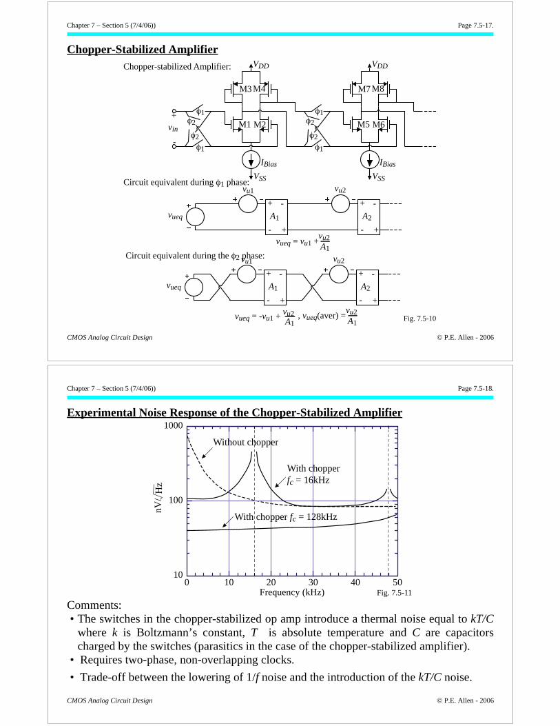
Chapter 7 – Section 5 (7/4/06)) Page 7.5-17.
CMOS Analog Circuit Design © P.E. Allen - 2006
Chopper-Stabilized Amplifier VDD
VSS
φ1
φ1
φ2
φ2
IBias
M1 M2
M3 M4
+
-
vin
VDD
VSS
φ1
φ1
φ2
φ2
IBias
M5 M6
M7 M8
Circuit equivalent during φ1 phase:
A1
+
-
-
+
A2
+
-
-
+
vu2vu1
vueq
Circuit equivalent during the φ2 phase:
A1
+
-
-
+
A2
+
-
-
+
vu2vu1
vueq
vueq = vu1 + vu2A1
vueq = -vu1 + A1
vu2 , vueq(aver) = vu2A1
Fig. 7.5-10
Chopper-stabilized Amplifier:
Chapter 7 – Section 5 (7/4/06)) Page 7.5-18.
CMOS Analog Circuit Design © P.E. Allen - 2006
Experimental Noise Response of the Chopper-Stabilized Amplifier
10
100
1000
0 10 20 30 40 50Frequency (kHz)
nV/
Hz
Without chopper
With chopperfc = 16kHz
With chopper fc = 128kHz
Fig. 7.5-11 Comments: • The switches in the chopper-stabilized op amp introduce a thermal noise equal to kT/C
where k is Boltzmann’s constant, T is absolute temperature and C are capacitors charged by the switches (parasitics in the case of the chopper-stabilized amplifier).
• Requires two-phase, non-overlapping clocks.
• Trade-off between the lowering of 1/f noise and the introduction of the kT/C noise.
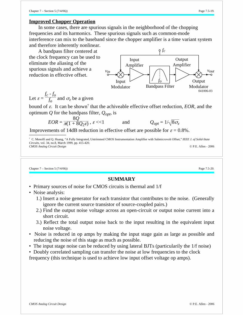
Chapter 7 – Section 5 (7/4/06)) Page 7.5-19.
CMOS Analog Circuit Design © P.E. Allen - 2006
Improved Chopper Operation In some cases, there are spurious signals in the neighborhood of the chopping frequencies and its harmonics. These spurious signals such as common-mode interference can mix to the baseband since the chopper amplifier is a time variant system and therefore inherently nonlinear. A bandpass filter centered at the clock frequency can be used to eliminate the aliasing of the spurious signals and achieve a reduction in effective offset.
Let = fc - fo
fo and be a given
bound of . It can be shown† that the achiveable effective offset reduction, EOR, and the optimum Q for the bandpass filter, Qopt, is
† C. Menolfi and Q. Huang, “A Fully Integrated, Untrimmed CMOS Instrumentation Amplifier with Submicrovolt Offset,” IEEE J. of Solid-State Circuits, vol. 34, no.8, March 1999, pp. 415-420.
Bandpass Filter
fc
InputModulator
InputAmplifier
OutputAmplifier
OutputModulator
vin vout
fo
041006-03
EOR = 8Q
(1 + 8Q2 ) , <<1 and Qopt = 1/ 8
Improvements of 14dB reduction in effective offset are possible for = 0.8%.
Chapter 7 – Section 5 (7/4/06)) Page 7.5-20.
CMOS Analog Circuit Design © P.E. Allen - 2006
SUMMARY
• Primary sources of noise for CMOS circuits is thermal and 1/f • Noise analysis:
1.) Insert a noise generator for each transistor that contributes to the noise. (Generally ignore the current source transistor of source-coupled pairs.)
2.) Find the output noise voltage across an open-circuit or output noise current into a short circuit.
3.) Reflect the total output noise back to the input resulting in the equivalent input noise voltage.
• Noise is reduced in op amps by making the input stage gain as large as possible and reducing the noise of this stage as much as possible.
• The input stage noise can be reduced by using lateral BJTs (particularily the 1/f noise) • Doubly correlated sampling can transfer the noise at low frequencies to the clock frequency (this technique is used to achieve low input offset voltage op amps).

Chapter 7 – Section 6 (7/4/06)) Page 7.6-1.
CMOS Analog Circuit Design © P.E. Allen - 2006
SECTION 7.6 – LOW VOLTAGE OP AMPS Objective
The objective of this presentation is:
1.) How to design standard circuit blocks with reduced power supply voltage
2.) Introduce new methods of designing low voltage circuits
Outline
• Low voltage input stages
• Low voltage gain stages
• Low voltage bias circuits
• Low voltage op amps
• Summary
Chapter 7 – Section 6 (7/4/06)) Page 7.6-2.
CMOS Analog Circuit Design © P.E. Allen - 2006
Implications of Low-Voltage, Strong-Inversion Operation
• Reduced power supply means decreased dynamic range
• Nonlinearity will increase because the transistor is working close to VDS(sat)
• Large values of because the transistor is working close to VDS(sat)
• Increased drain-bulk and source-bulk capacitances because they are less reverse biased.
• Large values of currents and W/L ratios to get high transconductance
• Small values of currents and large values of W/L will give smallVDS(sat)
• Severely reduced input common mode range
• Switches will require charge pumps

Chapter 7 – Section 6 (7/4/06)) Page 7.6-3.
CMOS Analog Circuit Design © P.E. Allen - 2006
What are the Limits of Power Supply?
The limit comes when there is no signal range left when the dc drops are subtracted from VDD.
Minimum power supply (no signal swing range):
VDD(min.) = VT + 2VON
For differential amplifiers, the minimum power supply is:
VDD(min.) = 3VON
However, to have any input common mode range, the effective minimum power supply is,
VDD(min.) = VT + 2VON
060802-01
VDD
VPB1
VNB1
M1
M2 M3
M4
+
−
VON
VT+VON
+
−
+
−VT+VON
VON
+
−
060802-02
VPB1
VDD
VNB1
+
−VON
+
−VON
+
−
VON +
−VT+VON
+
−VT+VON
M1 M2
M3 M4
M5
Chapter 7 – Section 6 (7/4/06)) Page 7.6-4.
CMOS Analog Circuit Design © P.E. Allen - 2006
Minimum Power Supply Limit – Continued
The previous consideration of the differential amplifier did not consider getting the signal out of the amplifier. This will add another VON.
060802-03
VPB1
VDD
VNB1
+
−VON
+
−VON
+
−
VON +
−VT+VON
+
−VT+VON
M1 M2
M3 M4
M5
VPB1
VPB2M6
M7 M8
M9
+
−VON
VT+VON+
−
VT
Therefore,
VDD(min.) = VT + 3VON
This could be reduced to 3VON with the floating battery but its implementation probably requires more than 3VON of power supply.
Note the output signal swing is VT + VON while the input common range is VON.
Chapter 7 – Section 6 (7/4/06)) Page 7.6-5.
CMOS Analog Circuit Design © P.E. Allen - 2006
LOW VOLTAGE INPUT STAGES
Input Common Mode Voltage Range
Minimum power supply (ICMR = 0):
VDD(min) = VSD3(sat)-VT1+VGS1+VDS5(sat) = VSD3(sat)+VDS1(sat)+VDS5(sat)
Input common-mode range:
Vicm(upper) = VDD - VSD3(sat) + VT1
Vicm(lower) = VDS5(sat) + VGS1
If the threshold magnitudes are 0.7V, VDD = 1.5V and the saturation voltages are 0.3V, then
Vicm(upper) = 1.5 - 0.3 + 0.7 = 1.9V and Vicm(lower) = 0.3 + 1.0 = 1.3V
giving an ICMR of 0.6V.
vicm M1 M2
M3 M4
M5
VDD
VDS5(sat)VBias
+
-
VBias+
-
VGS1
-VT1
VSD3(sat)
Fig. 7.6-3
Chapter 7 – Section 6 (7/4/06)) Page 7.6-6.
CMOS Analog Circuit Design © P.E. Allen - 2006
Increasing ICMR using Parallel Input Stages Turn-on voltage for the n-channel input: Vonn = VDSN5(sat) + VGSN1 Turn-on voltage for the p-channel input: Vonp = VDD - VSDP5(sat) - VSGP1 The sum of Vonn and Vonp equals the minimum power supply. Regions of operation: VDD > Vicm > Vonp: (n-channel on and p-channel off) gm(eq) = gmN
Vonp Vicm Vonn: (n-channel on and p-channel on) gm(eq) = gmN + gmP
Vonn > Vicm > 0 : (n-channel off and p-channel on) gm(eq) = gmP
where gm(eq) is the equivalent input transconductance of the above input stage, gmN is the input transconductance for the n-channel input and gmP is the input transconduct-ance for the p-channel input.
VDD
MN1 MN2MP1 MP2
MP3MP4
MP5MN3MN4
MN5
IBias
M6
M7
Fig. 7.6-4
Vicm Vicm
0 VSDP5(sat)+VGSN1 VDD-VSDP5(sat)+VGSN1 VDD
gmN+gmP
gmNgmP
gm(eff)
Vicm
n-channel onn-channel off n-channel onp-channel onp-channel on p-channel off
Fig. 7.6-5
Vonn Vonp
Chapter 7 – Section 6 (7/4/06)) Page 7.6-7.
CMOS Analog Circuit Design © P.E. Allen - 2006
Removing the Nonlinearity in Transconductances as a Function of ICMR Increase the bias current in the different-ial amplifier that is on when the other differential amplifier is off.
Three regions of operation depending on the value of Vicm: 1.) Vicm < Vonn: n-channel diff. amp.
off and p-channel on with Ip = 4Ib:
gm(eff) = KP’WP
LP 2 Ib
2.) Vonn < Vicm < Vonp: both on with In = Ip = Ib:
gm(eff) = KN’WN
LN Ib +
KP’WPLP
Ib
3.) Vicm > Vonp: p-channel diff. amp. off and n-channel on with In = 4Ib:
gm(eff) = KN’WN
LN 2 Ib
VDD
Ib
Ib1:3
3:1
MN1
MP1 MP2
MN2MB2 MB1
VB2 VB1
Inn
Ipp
Ip
In
VicmVicm
Fig. 7.6-6
Chapter 7 – Section 6 (7/4/06)) Page 7.6-8.
CMOS Analog Circuit Design © P.E. Allen - 2006
How Does the Current Compensation Work? Set VB1 = Vonn and VB2 = Vonp.
VonnMN1 MN2
MB1vicmvicm
IppIn
IbIf vicm >Vonn then In = Ib and Ipp=0
If vicm <Vonn then In = 0 and Ipp=Ib
VDD
Vonp
MP1 MP2
MB2vicmvicm
Inn Ip
IbIf vicm <Vonp then Ip = Ib and Inn=0
If vicm >Vonp then Ip = 0 and Inn=Ib
Fig. 7.6-6A Result:
gm(eff)
Vonn Vonp VDD
Vicm00
gmN=gmP
Fig. 7.6-7 The above techniques and many similar ones are good for power supply values down to about 1.5V. Below that, different techniques must be used or the technology must be modified (natural devices).
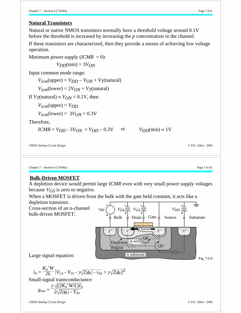
Chapter 7 – Section 6 (7/4/06)) Page 7.6-9.
CMOS Analog Circuit Design © P.E. Allen - 2006
Natural Transistors
Natural or native NMOS transistors normally have a threshold voltage around 0.1V before the threshold is increased by increasing the p concentration in the channel.
If these transistors are characterized, then they provide a means of achieving low voltage operation.
Minimum power supply (ICMR = 0):
VDD(min) = 3VON
Input common mode range:
Vicm(upper) = VDD – VON + VT(natural)
Vicm(lower) = 2VON + VT(natural)
If VT(natural) VON = 0.1V, then
Vicm(upper) = VDD
Vicm(lower) = 3VON = 0.3V
Therefore,
ICMR = VDD - 3VON = VDD – 0.3V VDD(min) 1V
Chapter 7 – Section 6 (7/4/06)) Page 7.6-10.
CMOS Analog Circuit Design © P.E. Allen - 2006
Bulk-Driven MOSFET A depletion device would permit large ICMR even with very small power supply voltages because VGS is zero or negative. When a MOSFET is driven from the bulk with the gate held constant, it acts like a depletion transistor. Cross-section of an n-channel bulk-driven MOSFET:
Large signal equation:
iD = KN’W
2L VGS - VT0 - 2| F| - vBS + 2| F| 2
Small-signal transconductance:
gmbs = (2KN’W/L)ID
2 2| F| - VBS
����
p-well
n+
����n+
����n+
����p+ Channel
����������������
QP
QV
Bulk Drain Gate Source Substrate
VDDVGSVDSvBS
DepletionRegion
n substrateFig. 7.6-8
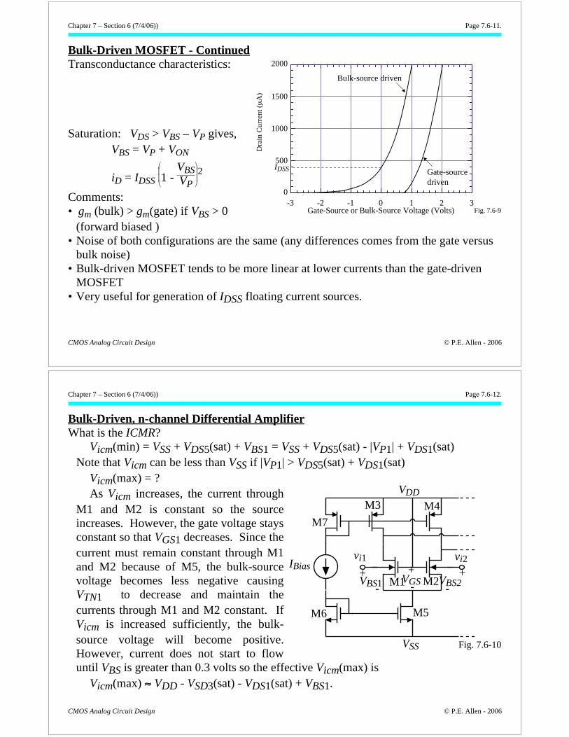
Chapter 7 – Section 6 (7/4/06)) Page 7.6-11.
CMOS Analog Circuit Design © P.E. Allen - 2006
Bulk-Driven MOSFET - Continued Transconductance characteristics:
Saturation: VDS > VBS – VP gives, VBS = VP + VON
iD = IDSS 1 - VBSVP
2
Comments: • gm (bulk) > gm(gate) if VBS > 0
(forward biased ) • Noise of both configurations are the same (any differences comes from the gate versus
bulk noise) • Bulk-driven MOSFET tends to be more linear at lower currents than the gate-driven
MOSFET • Very useful for generation of IDSS floating current sources.
0
500
1000
1500
2000
-3 -2 -1 0 1 2 3
Dra
in C
urre
nt (μ
A)
Gate-Source or Bulk-Source Voltage (Volts)
IDSS
Bulk-source driven
Gate-sourcedriven
Fig. 7.6-9
Chapter 7 – Section 6 (7/4/06)) Page 7.6-12.
CMOS Analog Circuit Design © P.E. Allen - 2006
Bulk-Driven, n-channel Differential Amplifier What is the ICMR? Vicm(min) = VSS + VDS5(sat) + VBS1 = VSS + VDS5(sat) - |VP1| + VDS1(sat) Note that Vicm can be less than VSS if |VP1| > VDS5(sat) + VDS1(sat) Vicm(max) = ? As Vicm increases, the current through
M1 and M2 is constant so the source increases. However, the gate voltage stays constant so that VGS1 decreases. Since the current must remain constant through M1 and M2 because of M5, the bulk-source voltage becomes less negative causing VTN1 to decrease and maintain the currents through M1 and M2 constant. If Vicm is increased sufficiently, the bulk-source voltage will become positive. However, current does not start to flow until VBS is greater than 0.3 volts so the effective Vicm(max) is
Vicm(max) VDD - VSD3(sat) - VDS1(sat) + VBS1.
VDD
VSS
M1 M2
M3 M4
M5M6
M7
IBiasvi1 vi2
Fig. 7.6-10
+ VBS1-
+ VBS2-
+ VGS-
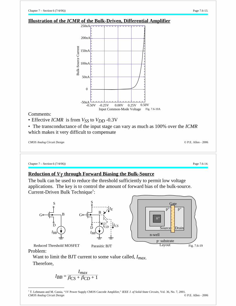
Chapter 7 – Section 6 (7/4/06)) Page 7.6-13.
CMOS Analog Circuit Design © P.E. Allen - 2006
Illustration of the ICMR of the Bulk-Driven, Differential Amplifier
-50nA
0
50nA
100nA
150nA
Bul
k-So
urce
Cur
rent
Input Common-Mode Voltage-0.50V -0.25V 0.00V 0.25V 0.50V
200nA
250nA
Fig. 7.6-10A Comments: • Effective ICMR is from VSS to VDD -0.3V • The transconductance of the input stage can vary as much as 100% over the ICMR which makes it very difficult to compensate
Chapter 7 – Section 6 (7/4/06)) Page 7.6-14.
CMOS Analog Circuit Design © P.E. Allen - 2006
Reduction of VT through Forward Biasing the Bulk-Source
The bulk can be used to reduce the threshold sufficiently to permit low voltage applications. The key is to control the amount of forward bias of the bulk-source. Current-Driven Bulk Technique†:
IBB
S
G
D
B
IBB
S
G
D
BIE
ICD ICS
Reduced Threshold MOSFET Parasitic BJT
n-well
p+ p+
n+
����
Source Drain
Gate
p- substrateLayout Fig. 7.6-19
Problem: Want to limit the BJT current to some value called, Imax. Therefore,
IBB = Imax
CS + CD + 1
† T. Lehmann and M. Cassia, “1V Power Supply CMOS Cascode Amplifier,” IEEE J. of Solid-State Circuits, Vol. 36, No. 7, 2001.
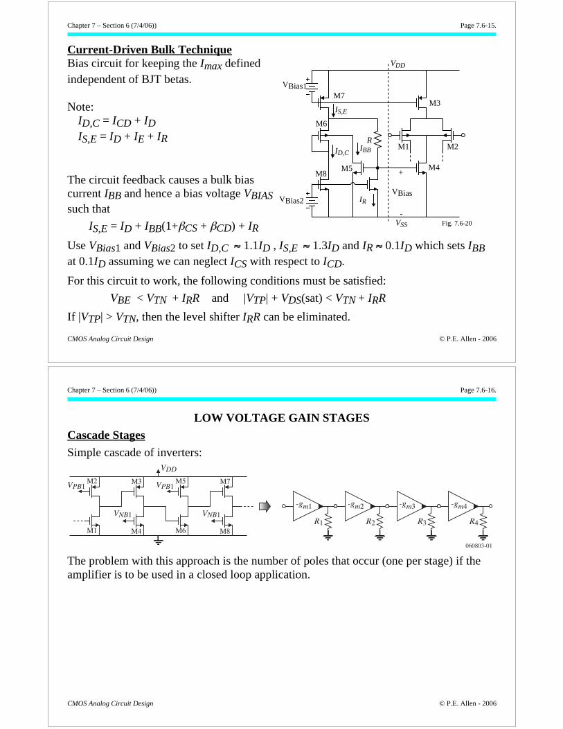
Chapter 7 – Section 6 (7/4/06)) Page 7.6-15.
CMOS Analog Circuit Design © P.E. Allen - 2006
Current-Driven Bulk Technique Bias circuit for keeping the Imax defined independent of BJT betas. Note: ID,C = ICD + ID IS,E = ID + IE + IR The circuit feedback causes a bulk bias current IBB and hence a bias voltage VBIAS such that
IS,E = ID + IBB(1+ CS + CD) + IR
Use VBias1 and VBias2 to set ID,C 1.1ID , IS,E 1.3ID and IR 0.1ID which sets IBB at 0.1ID assuming we can neglect ICS with respect to ICD.
For this circuit to work, the following conditions must be satisfied:
VBE < VTN + IRR and |VTP| + VDS(sat) < VTN + IRR
If |VTP| > VTN, then the level shifter IRR can be eliminated.
M1 M2
M3
M4M5
M6
M7
VDD
VSS
VBias1
M8
VBias2VBias
IBB
IS,E
ID,C
Fig. 7.6-20
R
IR
+
-
Chapter 7 – Section 6 (7/4/06)) Page 7.6-16.
CMOS Analog Circuit Design © P.E. Allen - 2006
LOW VOLTAGE GAIN STAGES
Cascade Stages
Simple cascade of inverters:
060803-01
VDD
VPB1
VNB1
M1
M2 M3
M4
VPB1
M6
M5
VNB1
M7
M8
-gm1
R1
-gm2
R2
-gm3
R3
-gm4
R4
The problem with this approach is the number of poles that occur (one per stage) if the amplifier is to be used in a closed loop application.
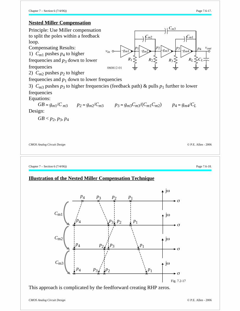
Chapter 7 – Section 6 (7/4/06)) Page 7.6-17.
CMOS Analog Circuit Design © P.E. Allen - 2006
Nested Miller Compensation
Principle: Use Miller compensation to split the poles within a feedback loop. Compensating Results: 1) Cm1 pushes p4 to higher frequencies and p3 down to lower frequencies 2) Cm2 pushes p2 to higher frequencies and p1 down to lower frequencies 3) Cm3 pushes p3 to higher frequencies (feedback path) & pulls p1 further to lower frequencies Equations: GB gm1/C m3 p2 gm2/Cm3 p3 gm3Cm3/(Cm1Cm2) p4 gm4/CL Design:
GB < p2, p3, p4
060812-01
vinvout-gm3-gm2-gm1 -gm4
Cm3
Cm1Cm2
p1 p2 p3 p4
R2R1 R3 RL CL
Chapter 7 – Section 6 (7/4/06)) Page 7.6-18.
CMOS Analog Circuit Design © P.E. Allen - 2006
Illustration of the Nested Miller Compensation Technique
jω
σp4 p3 p2 p1
jω
σp4 p3 p2 p1
jω
σp4 p3p2 p1
jω
σp4 p3 p2 p1
Cm1
Cm2
Cm3
Fig. 7.2-17 This approach is complicated by the feedforward creating RHP zeros.
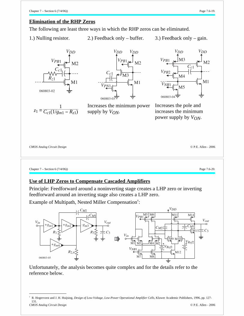
Chapter 7 – Section 6 (7/4/06)) Page 7.6-19.
CMOS Analog Circuit Design © P.E. Allen - 2006
Elimination of the RHP Zeros
The following are least three ways in which the RHP zeros can be eliminated.
1.) Nulling resistor.
060803-02
VDD
VPB1
Rz1
Cc1
M2
M1
z1 = 1
Cc1(1/gm1 Rz1)
2.) Feedback only – buffer.
060803-03
VDD
VPB1
Cc1
M2
M1VPN1
VDD
M3
Increases the minimum power supply by VON.
3.) Feedback only – gain.
060803-04
VDD
VPB1
Cc1M2
M1
VDD
VPB2
VNB1
M3
M4
M5
Increases the pole and increases the minimum power supply by VON.
Chapter 7 – Section 6 (7/4/06)) Page 7.6-20.
CMOS Analog Circuit Design © P.E. Allen - 2006
Use of LHP Zeros to Compensate Cascaded Amplifiers
Principle: Feedforward around a noninverting stage creates a LHP zero or inverting feedforward around an inverting stage also creates a LHP zero.
Example of Multipath, Nested Miller Compensation†:
060803-05
R3
+gm4
VoutVin
C3
+gm2+gm1
R1
-gm3
R2,4
M1 M2M3 M4
CM1
CM2
M8
VNB1
M7
VDD
VPB1M5 M6
VRef1
M12
M11
VRef2
M14
Vout
C3Vin
M9 M10
M13
CM1CM2
Unfortunately, the analysis becomes quite complex and for the details refer to the reference below.
† R. Hogervorst and J. H. Huijsing, Design of Low-Voltage, Low-Power Operational Amplifier Cells, Kluwer Academic Publishers, 1996, pp. 127-
131.
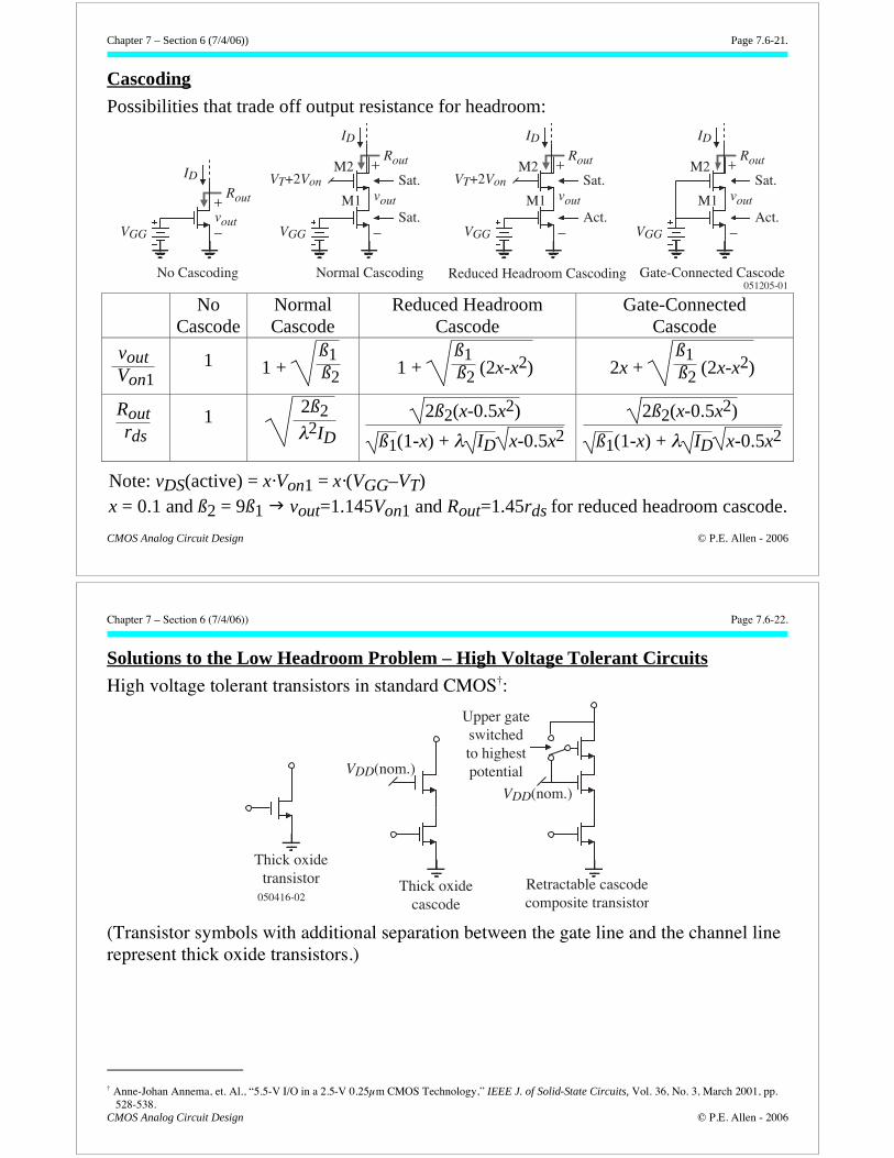
Chapter 7 – Section 6 (7/4/06)) Page 7.6-21.
CMOS Analog Circuit Design © P.E. Allen - 2006
Cascoding
Possibilities that trade off output resistance for headroom:
051205-01
VGG
ID
+
−vout
Rout
No Cascoding
VGG
ID
+
−
vout
Rout
Normal Cascoding
M1
M2Sat.
Sat.
VT+2Von
VGG
ID
+
−
vout
Rout
Reduced Headroom Cascoding
M1
M2Sat.
Act.
VT+2Von
VGG
ID
+
−
vout
Rout
Gate-Connected Cascode
M1
M2Sat.
Act.
No
Cascode Normal Cascode
Reduced Headroom Cascode
Gate-Connected Cascode
vout Von1 1 1 +
ß1 ß2 1 +
ß1 ß2 (2x-x2) 2x +
ß1 ß2 (2x-x2)
Rout rds 1 2ß2
2ID
2ß2(x-0.5x2)
ß1(1-x) + ID x-0.5x2 2ß2(x-0.5x2)
ß1(1-x) + ID x-0.5x2
Note: vDS(active) = x·Von1 = x·(VGG–VT) x = 0.1 and ß2 = 9ß1 vout=1.145Von1 and Rout=1.45rds for reduced headroom cascode.
Chapter 7 – Section 6 (7/4/06)) Page 7.6-22.
CMOS Analog Circuit Design © P.E. Allen - 2006
Solutions to the Low Headroom Problem – High Voltage Tolerant Circuits
High voltage tolerant transistors in standard CMOS†:
050416-02
Thick oxidetransistor Thick oxide
cascode
VDD(nom.)
VDD(nom.)
Upper gateswitchedto highestpotential
Retractable cascodecomposite transistor
(Transistor symbols with additional separation between the gate line and the channel line represent thick oxide transistors.)
† Anne-Johan Annema, et. Al., “5.5-V I/O in a 2.5-V 0.25μm CMOS Technology,” IEEE J. of Solid-State Circuits, Vol. 36, No. 3, March 2001, pp.
528-538.
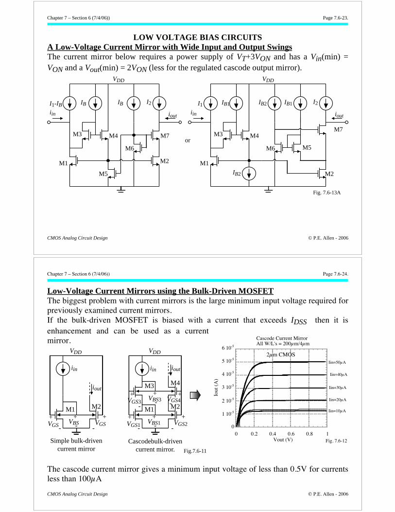
Chapter 7 – Section 6 (7/4/06)) Page 7.6-23.
CMOS Analog Circuit Design © P.E. Allen - 2006
LOW VOLTAGE BIAS CIRCUITS A Low-Voltage Current Mirror with Wide Input and Output Swings The current mirror below requires a power supply of VT+3VON and has a Vin(min) = VON and a Vout(min) = 2VON (less for the regulated cascode output mirror).
iin
M1 M2
M3
VDD
IB
M4
M5
M6
M7
iout
I1-IB IB I2
or
iin
M1
M2
M3
VDD
IB1
M4
M5M6
M7
iout
I1 IB2 I2IB1
IB2
Fig. 7.6-13A
Chapter 7 – Section 6 (7/4/06)) Page 7.6-24.
CMOS Analog Circuit Design © P.E. Allen - 2006
Low-Voltage Current Mirrors using the Bulk-Driven MOSFET The biggest problem with current mirrors is the large minimum input voltage required for previously examined current mirrors. If the bulk-driven MOSFET is biased with a current that exceeds IDSS then it is enhancement and can be used as a current mirror.
VDD
iin
iout
M1 M2
+
-VGS
+-
VBS+
-VGS
VDD
iin iout
M1 M2
+
-VGS1
+-
VBS1+
-VGS2
M3 M4
Simple bulk-driven current mirror
Cascodebulk-driven current mirror. Fig.7.6-11
+-
VBS3+
-VGS3
+-
VGS4
The cascode current mirror gives a minimum input voltage of less than 0.5V for currents less than 100μA
0
1 10-5
2 10-5
3 10-5
4 10-5
5 10-5
6 10-5
0 0.2 0.4 0.6 0.8 1
Cascode Current MirrorAll W/L's = 200μm/4μm
Iout
(A
)
Vout (V)
Iin=50μA
Iin=40μA
Iin=30μA
Iin=20μA
Iin=10μA
2μm CMOS
Fig. 7.6-12
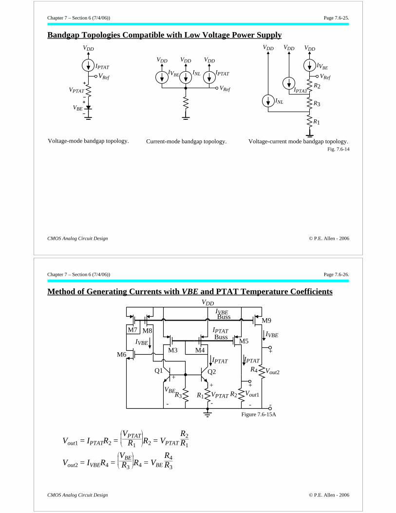
Chapter 7 – Section 6 (7/4/06)) Page 7.6-25.
CMOS Analog Circuit Design © P.E. Allen - 2006
Bandgap Topologies Compatible with Low Voltage Power Supply
VPTAT
VBE
IPTAT
VRef
VDD
Voltage-mode bandgap topology.
INL
VRef
VDD
IVBE
VDD
IPTAT
VDD
Current-mode bandgap topology.
VRef
VDD
IPTAT
VDDVDD
INL
IVBE
R2
R3
R1
Voltage-current mode bandgap topology.Fig. 7.6-14
Chapter 7 – Section 6 (7/4/06)) Page 7.6-26.
CMOS Analog Circuit Design © P.E. Allen - 2006
Method of Generating Currents with VBE and PTAT Temperature Coefficients
M3 M4M5
M6
M7
VDD
VPTATR1
+
-
Vout1
+
-
R2
Q1 Q2
IPTAT IPTAT
R3
Vout2
+
-
R4
IVBE
IVBEIPTATBuss
IVBEBuss
M8
M9
Figure 7.6-15A
VBE
+
-
Vout1 = IPTATR2 = VPTAT
R1R2 = VPTAT
R2R1
Vout2 = IVBER4 = VBER3
R4 = VBE
R4R3
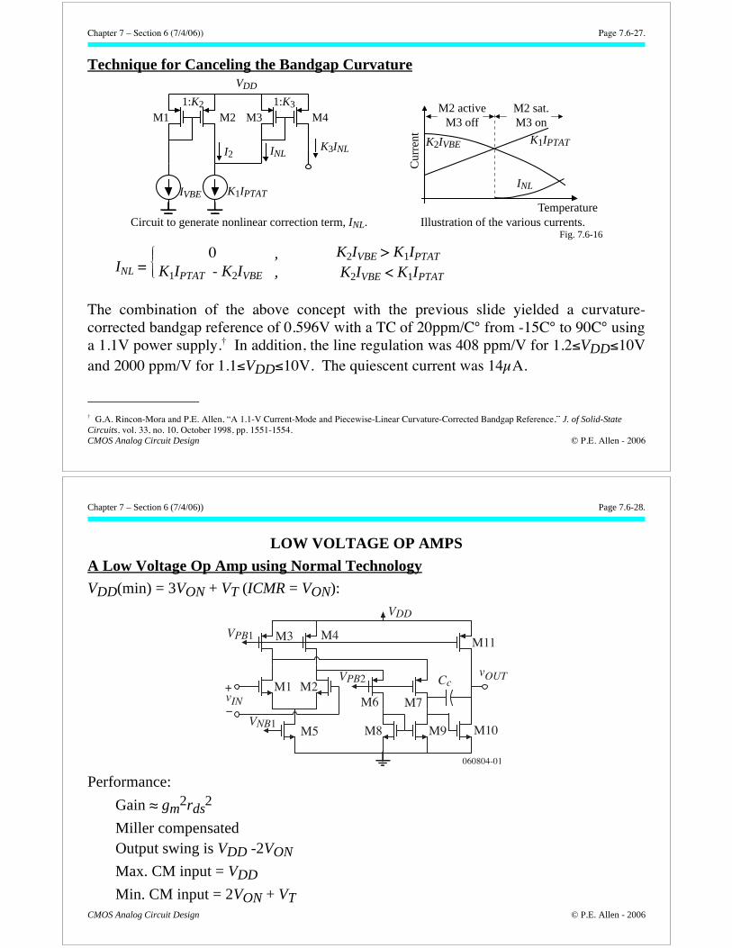
Chapter 7 – Section 6 (7/4/06)) Page 7.6-27.
CMOS Analog Circuit Design © P.E. Allen - 2006
Technique for Canceling the Bandgap Curvature VDD
M1 M2 M3 M4
IVBE K1IPTAT
1:K2 1:K3
I2 INLK3INL
Cur
rent K2IVBE K1IPTAT
Temperature
INL
M2 activeM3 off
M2 sat.M3 on
Circuit to generate nonlinear correction term, INL. Illustration of the various currents.Fig. 7.6-16
INL = 0
K1IPTAT - K2IVBE ,
, K2IVBE > K1IPTAT K2IVBE < K1IPTAT
The combination of the above concept with the previous slide yielded a curvature-corrected bandgap reference of 0.596V with a TC of 20ppm/C° from -15C° to 90C° using a 1.1V power supply.† In addition, the line regulation was 408 ppm/V for 1.2 VDD 10V and 2000 ppm/V for 1.1 VDD 10V. The quiescent current was 14μA.
† G.A. Rincon-Mora and P.E. Allen, “A 1.1-V Current-Mode and Piecewise-Linear Curvature-Corrected Bandgap Reference,” J. of Solid-State Circuits, vol. 33, no. 10, October 1998, pp. 1551-1554.
Chapter 7 – Section 6 (7/4/06)) Page 7.6-28.
CMOS Analog Circuit Design © P.E. Allen - 2006
LOW VOLTAGE OP AMPS
A Low Voltage Op Amp using Normal Technology
VDD(min) = 3VON + VT (ICMR = VON):
060804-01
VDD
VPB1
VNB1
VPB2
vIN+
−
vOUTM1 M2
M3 M4
M5
M6 M7
M8 M9 M10
M11
Cc
Performance:
Gain gm2rds
2
Miller compensated Output swing is VDD -2VON
Max. CM input = VDD
Min. CM input = 2VON + VT

Chapter 7 – Section 6 (7/4/06)) Page 7.6-29.
CMOS Analog Circuit Design © P.E. Allen - 2006
A Low-Voltage, Wide ICMR Op Amp
VDD(min) = 4VON + 2VT (ICMR = VDD):
3:1
1:3
041231-15
VDD
VDD-VT-VDS(sat)
VDD-VT-2VDS(sat)+ −
VT+VDS(sat)
VT+2VDS(sat)
vOUT
Performance:
Gain gm2rds
2, self compensated, and output swing is VDD -4VON
Chapter 7 – Section 6 (7/4/06)) Page 7.6-30.
CMOS Analog Circuit Design © P.E. Allen - 2006
An Alternate Low-Voltage, Wide ICMR Op Amp
VDD(min) = 4VON + 2VT (ICMR = VDD):
3:1
1:3060804-02
VDD
+ − vOUT
VPB2
VPB1
VPB2
VNB2
VNB1
VNB2

Chapter 7 – Section 6 (7/4/06)) Page 7.6-31.
CMOS Analog Circuit Design © P.E. Allen - 2006
A 1-Volt, Two-Stage Op Amp Uses a bulk-driven differential input amplifier.
vin+
vout
VDD=1V
IBias
Cc=30pF
CL
Rz=1kΩ
vin-
M1 M2
M3 M4Q5 Q6
M7
M8 M9 M10 M11M12
2000/2
400/2 400/2 400/2
6000/6 6000/6 3000/6 6000/6
Fig. 7.6-18
Chapter 7 – Section 6 (7/4/06)) Page 7.6-32.
CMOS Analog Circuit Design © P.E. Allen - 2006
Performance of the 1-Volt, Two-Stage Op Amp Specification (VDD=0.5V, VSS=-0.5V) Measured Performance (CL = 22pF)
DC open-loop gain 49dB (Vicm mid range) Power supply current 300μA Unity-gainbandwidth (GB) 1.3MHz (Vicm mid range) Phase margin 57° (Vicm mid range) Input offset voltage ±3mV Input common mode voltage range -0.475V to 0.450V Output swing -0.475V to 0.491V Positive slew rate +0.7V/μsec Negative slew rate -1.6V/μsec THD, closed loop gain of -1V/V -60dB (0.75Vp-p, 1kHz sinewave)
-59dB (0.75Vp-p, 10kHz sinewave) THD, closed loop gain of +1V/V -59dB (0.75Vp-p, 1kHz sinewave)
-57dB (0.75Vp-p, 10kHz sinewave) Spectral noise voltage density 367nV/ Hz @ 1kHz
181nV/ Hz @ 10kHz, 81nV/ Hz @ 100kHz 444nV/ Hz @ 1MHz
Positive Power Supply Rejection 61dB at 10kHz, 55dB at 100kHz, 22dB at 1MHz Negative Power Supply Rejection 45dB at 10kHz, 27dB at 100kHz, 5dB at 1MHz
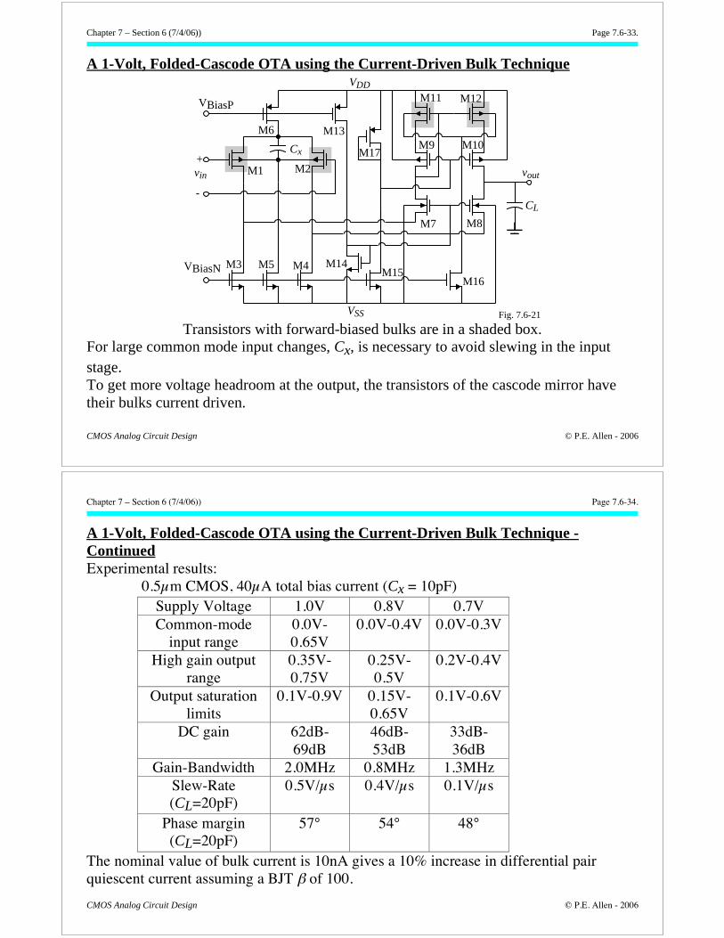
Chapter 7 – Section 6 (7/4/06)) Page 7.6-33.
CMOS Analog Circuit Design © P.E. Allen - 2006
A 1-Volt, Folded-Cascode OTA using the Current-Driven Bulk Technique
-
+vin M1 M2
M3 M4M5
M6
M7
vout
VDD
VSS
VBiasN
Cx
CL
VBiasP
M8
M9 M10
M11 M12
M13
M14M15
M16
M17
Fig. 7.6-21 Transistors with forward-biased bulks are in a shaded box.
For large common mode input changes, Cx, is necessary to avoid slewing in the input stage. To get more voltage headroom at the output, the transistors of the cascode mirror have their bulks current driven.
Chapter 7 – Section 6 (7/4/06)) Page 7.6-34.
CMOS Analog Circuit Design © P.E. Allen - 2006
A 1-Volt, Folded-Cascode OTA using the Current-Driven Bulk Technique - Continued Experimental results: 0.5μm CMOS, 40μA total bias current (Cx = 10pF) Supply Voltage 1.0V 0.8V 0.7V Common-mode
input range 0.0V-0.65V
0.0V-0.4V 0.0V-0.3V
High gain output range
0.35V-0.75V
0.25V-0.5V
0.2V-0.4V
Output saturation limits
0.1V-0.9V 0.15V-0.65V
0.1V-0.6V
DC gain 62dB-69dB
46dB-53dB
33dB-36dB
Gain-Bandwidth 2.0MHz 0.8MHz 1.3MHz Slew-Rate
(CL=20pF) 0.5V/μs 0.4V/μs 0.1V/μs
Phase margin (CL=20pF)
57° 54° 48°
The nominal value of bulk current is 10nA gives a 10% increase in differential pair quiescent current assuming a BJT of 100.
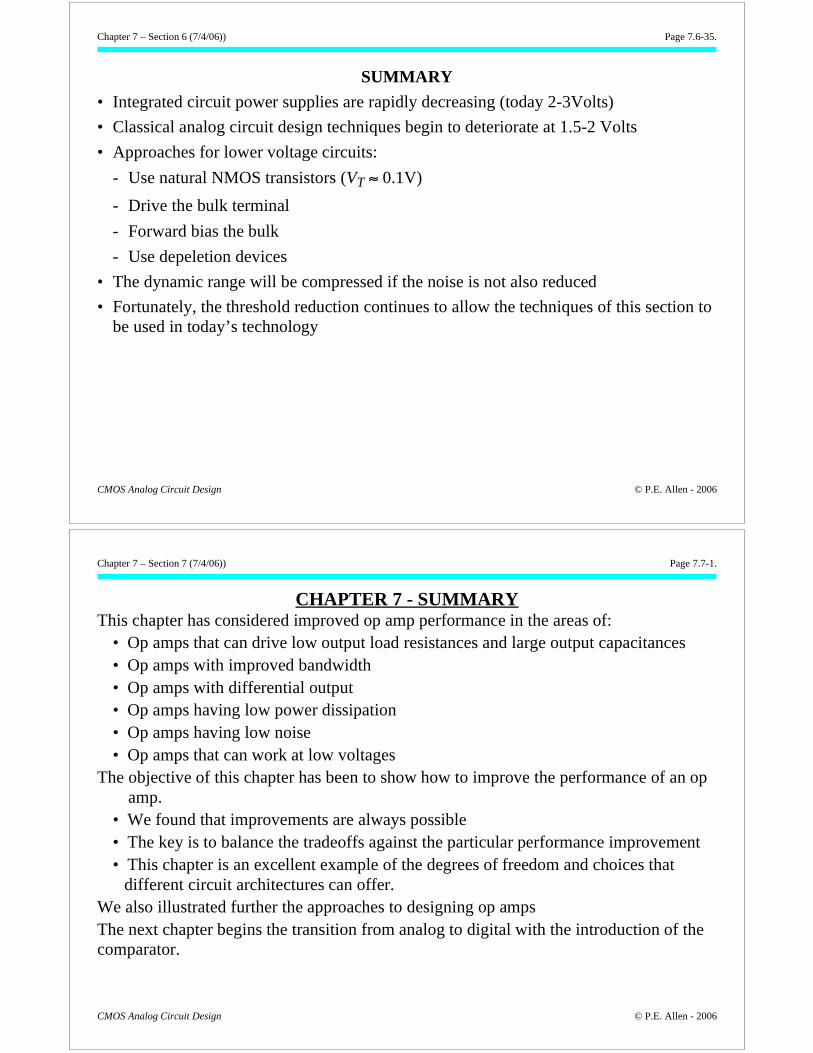
Chapter 7 – Section 6 (7/4/06)) Page 7.6-35.
CMOS Analog Circuit Design © P.E. Allen - 2006
SUMMARY
• Integrated circuit power supplies are rapidly decreasing (today 2-3Volts)
• Classical analog circuit design techniques begin to deteriorate at 1.5-2 Volts
• Approaches for lower voltage circuits:
- Use natural NMOS transistors (VT 0.1V)
- Drive the bulk terminal
- Forward bias the bulk
- Use depeletion devices
• The dynamic range will be compressed if the noise is not also reduced
• Fortunately, the threshold reduction continues to allow the techniques of this section to be used in today’s technology
Chapter 7 – Section 7 (7/4/06)) Page 7.7-1.
CMOS Analog Circuit Design © P.E. Allen - 2006
CHAPTER 7 - SUMMARY This chapter has considered improved op amp performance in the areas of:
• Op amps that can drive low output load resistances and large output capacitances • Op amps with improved bandwidth • Op amps with differential output • Op amps having low power dissipation • Op amps having low noise • Op amps that can work at low voltages
The objective of this chapter has been to show how to improve the performance of an op amp.
• We found that improvements are always possible • The key is to balance the tradeoffs against the particular performance improvement • This chapter is an excellent example of the degrees of freedom and choices that
different circuit architectures can offer. We also illustrated further the approaches to designing op amps The next chapter begins the transition from analog to digital with the introduction of the comparator.