Chapter 7 Hardware Reference 7 Hardware Reference MPC-684 Main CPU Board This upward compatible...
44
Chapter 7 Hardware Reference MPC-684 Main CPU Board This upward compatible board is two times faster in comparison with the MPC-68K. The following features are added to 68K: 1. RTC cannot be installed. (In 68K, it is option.) 2. J3 pulse port is no longer available. 3. User interruption INT2 does not exit. 4. To use the functions registered in USERCOM area, a coprocessor is required. The RS-232 port is activated by a DC 5V provided from J5 DC through a step down regulator J5 DC. Therefore, it is isolated from the internal circuit from the standpoint of noise. Program port (CH1) works at 19200 bps, which means a shorter time for loading the program. Specification Coprocessor MC68882FN25 (option) ROM Two 29F040 (4Mx2) RAM Two HM628512 (4Mx2 battery backup) RS-232 Photo coupler isolate 3CH CH0 for user CH1 for program (9600bps as a standard,ParityNone,data 8Bit,stop bit 1) CH2 for user I/O Input 8 photo coupler isolate input (for origin sensor) Output 4 photo coupler isolate output(auxiliary otput for I/F, DC24V 50mA(max)) Interruption INT1 I/O bus C BUS-compliant A0=LO, (BHE)=(UDS) Memory access is not available.((IORD), (IOWR)) *Signal name () means “L”, which indicates active. Power source DC12~24V(I/O activation, consumption current, 100 mA or less) Consumption current DC5V 300mA When providing DC 5V from J5, F1 short (factory setting) When providing DC 5V from bus, F1 open (F1 is 1 A fuse) Bus power supply ability 700 mA or less (loaded power source is 1 A) Service temperature 0~50ºC Buttery maintenance CR2032, maintenance period 5 years (1μA 22ºC storage) Interpreter ADVFSC 32 multi task loaded
Transcript of Chapter 7 Hardware Reference 7 Hardware Reference MPC-684 Main CPU Board This upward compatible...

Chapter 7 Hardware Reference
MPC-684 Main CPU Board
This upward compatible board is two times faster in comparison with the MPC-68K. The following features are added to 68K: 1. RTC cannot be installed. (In 68K, it is option.) 2. J3 pulse port is no longer available. 3. User interruption INT2 does not exit. 4. To use the functions registered in USERCOM area, a coprocessor is required.
The RS-232 port is activated by a DC 5V provided from J5 DC through a step down regulator J5 DC. Therefore, it is isolated from the internal circuit from the standpoint of noise. Program port (CH1) works at 19200 bps, which means a shorter time for loading the program.
Specification Coprocessor MC68882FN25 (option) ROM Two 29F040 (4Mx2) RAM Two HM628512 (4Mx2 battery backup) RS-232 Photo coupler isolate 3CH CH0 for user CH1 for program (9600bps as a standard,ParityNone,data 8Bit,stop bit 1) CH2 for user I/O Input 8 photo coupler isolate input (for origin sensor) Output 4 photo coupler isolate output(auxiliary otput for I/F, DC24V 50mA(max)) Interruption INT1 I/O bus C BUS-compliant A0=LO, (BHE)=(UDS) Memory access is not available.((IORD), (IOWR)) *Signal name () means “L”, which indicates active. Power source DC12~24V(I/O activation, consumption current, 100 mA or less) Consumption current DC5V 300mA When providing DC 5V from J5, F1 short (factory setting) When providing DC 5V from bus, F1 open (F1 is 1 A fuse) Bus power supply ability 700 mA or less (loaded power source is 1 A) Service temperature 0~50ºC Buttery maintenance CR2032, maintenance period 5 years (1µA 22ºC storage) Interpreter ADVFSC 32 multi task loaded

Hardware Configuration
BAT
J3
J1
LED1,LED2
J2
J4
J5
F1 SP7,SP8
CEP-054FMPC-684
ACCEL CORP.
CR2032
Accessories: (1) Power connector (H4P-SHF-AA) JST * 1 J5 (2) Contact (BHF-001T-0.8SS) JST * 4 J5 Mounted connectors J1, J2, J3 HIF-3FC10PA-2.54DS Hirose J4 HIF-3FC10PA-2.54DS Hirose J5 BS4P-SHF-1AA JST JST
J1 RS-232C (CH1 and CH2) J2 RS-232C (CH0) J4 I/O J5 Internal 5V, I/O-driving power supply JP1 DC 5V 1A fuse LED1 (Green) Power supply display LED2 (Red) Error display BAT SRAM backup buttery CR2032 SP7,8 CH1 board rate selection
Pin Assignment and Example of Connection (1)J1 RS-232C (CH1,H2)
1 SG 2 TXD1 3 RXD1 4 SG 5 MAN 6 [+5V] 7 SG 8 TXD2 9 RXD2 10 NC
CH1 for Program ( 8 bit, 1 stop fixed) CH2 for User (Initialized by cnfg#2 command)[+5V] is with a pull-up resister.
(2) RS-232C (CH0)
1 FG 2 TXD 3 RXD 4 RTS 5 CTS 6 NC 7 SG 8 NC 9 Key 10 DTR
CH0 for User (Initialized by cnfg#0 command)
(3)RS-232CH1 Board Rate Selection
SP7 SP8
9600 OPEN OPEN
19200 SHORT OPEN
* 9600 bps as default
. (4)J4 I/O Port (5)J5 Power Connector
1 3 5 7 9 11 13 15
IN1.XS1 IN3.YS1 IN5.US1 IN7.ZS1 OP1 OP3 GND +DC
2 4 6 8 10 12 14 16
IN2.XS2IN.4.YS2IN6.US2IN8.ZS2OP2 OP4 GND +DC
1234
+DC GND FG
+24V +DC J4-15,16 J5-1
GND J4-13,14J5-3
P_SW(n)
P_ON/OF
GND
6.2KR
Input/Output is the photo coupler type. Input is bringing over, while output is a photo coupler transistor open collector. The input current is adjustable with an SIP socket resistant array, 6.8KΩ as a standard implementation. The output transistor’s volume is 50 mA. (For TLP627) The input/ouput board is not insulated from board’s 5 V type. (DC is common, while AC cinludes L.) When the power supply is provided from J5, set F1(1 A fuse) to short, when bus line, set open. When DC 5V power is provided from MPS-324 or other power supply board, set F1 to open.
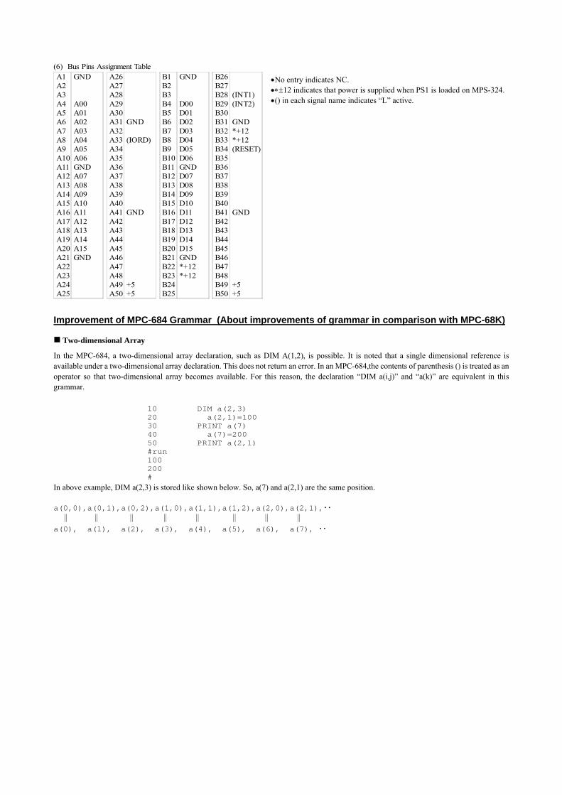
(6) Bus Pins Assignment Table A1 GND A26 B1 GND B26 A2 A27 B2 B27 A3 A28 B3 B28 (INT1) A4 A00 A29 B4 D00 B29 (INT2) A5 A01 A30 B5 D01 B30 A6 A02 A31 GND B6 D02 B31 GND A7 A03 A32 B7 D03 B32 *+12 A8 A04 A33 (IORD) B8 D04 B33 *+12 A9 A05 A34 B9 D05 B34 (RESET) A10 A06 A35 B10 D06 B35 A11 GND A36 B11 GND B36 A12 A07 A37 B12 D07 B37 A13 A08 A38 B13 D08 B38 A14 A09 A39 B14 D09 B39 A15 A10 A40 B15 D10 B40 A16 A11 A41 GND B16 D11 B41 GND A17 A12 A42 B17 D12 B42 A18 A13 A43 B18 D13 B43 A19 A14 A44 B19 D14 B44 A20 A15 A45 B20 D15 B45 A21 GND A46 B21 GND B46 A22 A47 B22 *+12 B47 A23 A48 B23 *+12 B48 A24 A49 +5 B24 B49 +5 A25 A50 +5 B25 B50 +5
•No entry indicates NC. •∗±12 indicates that power is supplied when PS1 is loaded on MPS-324. •() in each signal name indicates “L” active.
Improvement of MPC-684 Grammar (About improvements of grammar in comparison with MPC-68K)
Two-dimensional Array
In the MPC-684, a two-dimensional array declaration, such as DIM A(1,2), is possible. It is noted that a single dimensional reference is available under a two-dimensional array declaration. This does not return an error. In an MPC-684,the contents of parenthesis () is treated as an operator so that two-dimensional array becomes available. For this reason, the declaration “DIM a(i,j)” and “a(k)” are equivalent in this grammar.
10 DIM a(2,3) 20 a(2,1)=100 30 PRINT a(7) 40 a(7)=200 50 PRINT a(2,1) #run 100 200 #
In above example, DIM a(2,3) is stored like shown below. So, a(7) and a(2,1) are the same position. a(0,0),a(0,1),a(0,2),a(1,0),a(1,1),a(1,2),a(2,0),a(2,1),・・ ∥ ∥ ∥ ∥ ∥ ∥ ∥ ∥
a(0), a(1), a(2), a(3), a(4), a(5), a(6), a(7), ・・

Operator ";" and ","
"," Operator In the parenthesis, "," operator is word swap operator, before "," is upper word. Without parenthesis, “,” is delimitter as usual.
#PRX 1,2 1 2 #a=(1,2) #prx a 00010002
By using an operator, long composition of long in parallel input is easily realized. For example, since “WIR()” is for the loading I/O word, coding as “A=(WIR(&H80),WIR(&H82))” realize it as long. ";" Operator ";" operator shifts left part to MSB-side by 8 bits.
#a=1;2;3;4 /*1*&H1000000+2*&H10000+3*&H100+4 #prx a 01020304
Local Variables
In the MPC-684, local variables are available. A local variable is described as a “label!”. Even the same “label!” is assigned to a different variable area according to each task. By using this variable, several tasks can share the same subroutine, which is otherwise impossible. In addition, it can be used for a variable in a program that has the same pattern like a FOR-NEXT counter. A Local variable can be set up to 26. It is noted that, after stopping the program, executing a “PR label!” can refer only the value of task1’s label!. In the following example, although task1 and task2 share a common variable, the operation of an I/O area in each task is realized without conflict.
10 FORK 1 *sub1 20 FORK 2 *sub1 30 END 47 *sub1 65 DO 100 FOR count!=0 TO 23 110 out!=count!+(TASKN-1)*24 115 ON out! : TIME 50 : OFF out! 120 NEXT count! 130 LOOP
Delivery of Value to Subroutine and Reference of the Return ( REV-2.80t or later)
The difficulty in using the “GOSUB~RETURN” is the difficulty of the delivery of arguments and the reference of the return. For this reason, MPC-684 expands GOSUB and RETURN so that the delivery of the argument and the reference of the return become easier. GOSUB *label [arg1 arg2…] The list after the label can be passed to a subroutine. The receiver side executes “_VAR variable1, variable 2…. “ to receive the arguments.
10 GOSUB *SUB 1 2 3 20 END 30 *SUB 40 _VAR A B C /*receive arguments 50 PRINT A B C 60 RETURN #RUN
1 2 3
RETURN [arg1,arg2….] To receive the return, execute “_RET_VAL variable1, variable 2….”.
10 GOSUB *SUB 20 _RET_VAL A /*receive the return 30 PRINT A 40 END 50 *SUB 60 C=123 70 RETURN C /* C=return RUN 123
With a combination of local variables, several tasks can share the same subroutine.
10 GOSUB *SUB 1 2 20 _RET_VAL a 30 PRINT a 40 END 50 *SUB 60 _VAR a! b! /* In subroutine, loval variable is used. 70 c!=a!+b! 80 RETURN c! #RUN 3
BREAK Statement
BREAK statement ends the control flow, such as IF, DO-LOOP, WHILE-WEND and FOR-NEXT. BREAK in If-statement In an IF-statement, conditional branching with nesting becomes complicated. The use of BREAK in the IF-statement makes immediate escape from the relevant loop. It is noted that the use of BREAK in the If-statement requires END_IF as shown below.
IF a==1 THEN PRINT 777 ELSE IF b==1 THEN : PRINT a b : BREAK : END_IF IF b==2 THEN : PRINT "666" a b : BREAK : END_IF PRINT "555" END_IF (Next Step)
BREAK out of the LOOP, such as DO-LOOP, WHILE-WEND and FOR-NEXT In these loops, BREAK requires the termination command of the loop as the argument. BREAK ends a loop that is specified by the argument. In the following example, BREAK, in the loop of DO-LOOP, specifies to end the FOR-NEXT loop. Therefore, when the condition is met, it ends FOR-NEXTをBREAK, ignoring DO-LOOP. The arguments of BREAK-statement, such as LOOP, NEXT, and WEND, are defined as reserved constants, which means these constants must be written in upper case.
10 FOR i=1 TO 1000 15 j=0 20 DO UNTIL j==10 30 j=j+1 40 IF i==500 THEN : BREAK NEXT : END_IF 50 LOOP 60 NEXT i 70 PRINT i j #run 500 1 #

Improvement of I/O Operation
@( ) function , ?( ) function MPC’s switch input returns bit value. This causes the unexpected error when operates logical negation with NOT(), like “&HFFFFFFFE”. In such a case, use @() function to inverse “1” and “0”.
#pr @(1) 0
In case of a complicated logical operation of the input port, the description “HSW(n)” becomes too long. It is likely to violate the 37-character-limit of the expression. To write shorter, ?() function is prepared. The following example is equivalent to the previous version’s expression s1=&h1&NOT(HSW(-1)\HSW(-2)).
s1=@(?(-1)\?(-2))
4-byte bulk reading by Input function HIN() This is valid to MIP, MOP and IOP in I/O and memory I/O. Example in regular I/O
10 SETIO 20 ON 0 9 18 27 30 PRINT IN(24) IN(25) IN(26) IN(27) 40 a=HIN(&H80+24) /*Add &H80 to read 4 bytes successively 50 b=HIN(&H100+24) /*Add &H100 to read twice 4 bytes successively, compare and return 60 PRX a b #run 1 2 4 8 08040201 08040201 #
Example in memory I/O
20 ON -1 -10 -19 -28 30 PRINT IN(-1) IN(-2) IN(-3) IN(-4) 40 a=HIN(-1-&H80) /*Subtract &H80 to read 4 bytes successively 60 PRX a run 1 2 4 8 08040201 #
Support of Touch Panel (Digital GP series)
RS-232 CH0 and touch panel display (GP series) can be directly connected without communication program. Refer to PROTCOL MEWNET Command Reference. in

RS-232C Connection Examples H
ere are examples of connecting with the RS-232C port of PC(DOS/V).
1
7 8 9
10
2 3 4 5 6
SG NC Key DTR
FG TXD RXD RTS CTS NC
SG TXD1 RXD1 SG MAN (+DC) SG TXD2 RXD2 FG
7 8 9
10
2 3 4 5 6
1 CH1
CH2
J1
J2 CH0
MPC-684 PC RS-232C CH0 3-line cross wiring
CH1, CH2 Cross wiring
This is a RS-232C for the user. Initialization is done with CNFG#0
Program mode with pins 5 and 6 short-circuited, automatic execution mode with the pins open.
This is a RS-232C for the user. Initialization is done with CNFG#2. It has a 3-line cross wiring.
This is a RS-232C for the program. Connected with using the cable set
1234567
9
CDRXDTXDDTRSG DSRRTS
CI 8 CTS
1234567
9
CDRXDTXDDTRSG DSRRTS
CI 8 CTS
1234567
9
CDRXDTXDDTRSG DSRRTS
CI 8 CTS
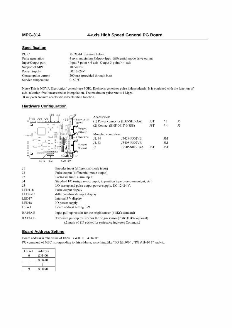
MPG-314 4-axis High Speed General PG Board
Specification PGIC MCX314 See note below. Pulse generation 4-axis maximum 4Mpps~1pps differential-mode drive output Input/Output port Input 7-point x 4-axis Output 3-point×4-axis Support of MPC 10 boards Power Supply DC12~24V Consumption current 200 mA (provided through bus) Service temperature 0~50 ºC Note) This is NOVA Electronics’ general-use PGIC. Each axis generates pulse independently. It is equipped with the function of axis-selection-free linear/circular interpolation. The maximum pulse rate is 4 Mpps. It supports S-curve acceleration/deceleration function.
Hardware Configuration
OC5 OC8
OC1 OC4
LED9-LED18DSW1
J1(upper)J3(lower)
LED1-LED8
J2(upper)J4(lower)
J5
RA17B,A
RA12RA14 RA6
MPG-314X
CEP-082B
ACCEL CORP.
SP3
U8
RA13
RA28
RA16A,B
Accessories: (1) Power connector (H4P-SHF-AA) JST * 1 J5 (2) Contact (BHF-001T-0.8SS) JST * 4 J5 Mounted connectors J2, J4 J3429-P302VE 3M J1, J3 J3408-P302VE 3M J5 BS4P-SHF-1AA JST JST
J1 Encoder input (differential-mode input) J3 Pulse output (differential-mode output) J2 Each-axis limit, alarm input J4 Standard I/O (origin sensor input, imposition input, servo on output, etc.) J5 I/O startup and pulse output power supply, DC 12~24 V. LED1~8 Pulse output dispaly LED9~15 differential-mode input display LED17 Internal 5 V display LED18 IO power supply DSW1 Board address setting 0~9
RA16A,B Input pull-up resister for the origin sensor (6.8KΩ standard)
RA17A,B Two-wire pull-up resistor for the origin sensor (2.7KΩ1/4W optional) (∆ mark of SIP socket for resistance indicates Common.)
Board Address Setting Board address is “the value of DSW1 x &H10 + &H400”. PG command of MPC is, responding to this address, something like “PG &H400” , “PG &H410 1” and etc.
DSW1 Address 0 &H400 1 &H410 | | 9 &H490

Pin Assignment Table
J1 Encoder Input
MPG-314 differential-mode Input Circuit
MCX314
470Ω 200Ω J1 odd
even
Inside of the parenthesis, subfunction
Note 1) X_AB~Z_AB is for absolute encoder input Note 2) X_IN2~U_IN2 is differential-mode input port *Insert TLP2630 in OC5~OC8 to validate this function. J1 is a differential-mode input interface. The positive “+” side is connected to the anode side of an internal photo coupler via 200 Ω-resistance, while the “–“ side is connected to a cathode. The LED9-16 is implemented as the polarity cancel diode of the photo coupler input. Therefore, lightning of LED signifies the signal OFF. In principle, it is encoder input (90° phase difference 2 phase clock). As a subfunction, it is connected to X-AB~Z-AB and X-IN2~Z-IN2. X-AB~Z-AB is the absolute encoder input port. It is available after the installment of one chip CPU, which is an option. X-IN2~Z-IN2 is connected to IN2, which is for the use of a condition stop. This input is used to receive the external condition stop input as the differential-mode signal.
J 3 pulse output
Monitor LED
Z
Y
A
GND
+(Even No.pin)
-(Odd No.pin)
+5V SN75172 J3 connector
TLP2630Twisted pair wires
This is a differential-mode output pulse interface. The standard CW/CCW two-pulse method can be changed to PULSE/DIR method through internal register setting.
J2 Each-axis Limit, alarm input
1 ~16 input: MCX314 to each input port 17~22 output: MCX314 to each Output Port (Includes J4-9,10) 23~26 origin sensor differential-mode input anode side Note) When SP4 short, X-ALM becomes valid ALM to all axes. The IN3 of each axis is used for the conditon stop and general use input. The LMTM, LMTP of each axis is for connecting with a limit sensor.(Always valid) The ALM of each axis is to connect with a servo alarm. (Valid on settings) The OUT4,OUT5 of each axis is a general output or the output of the result of counter comparison.
The signal of U-axis is displayed on J4. IN1(A) of each axis is for the differential-mode drive input to connect eacj-axis-S2 with Z phase (C phase). While each axis-S2 of J4 is connected with the cathode side, it is connected with anode side through RA28. Remove the RA17B to use this input.

J4 standard I/O(origin sensorinput, imposition input, servo on output 等)
1 X-INPOS 2 Y-INPOS 3 U-INPOS 4 Z-INPOS 5 X-SON (X-OUT0) 6 Y-SON (Y-OUT0) 7 U-SON (U-OUT0) 8 Z-SON (Z-OUT0) 9 U-OUT4 10 U-OUT5 11 IN1・XS1 (X-IN0) 12 IN2・XS2 (X-IN1)(K) 13 IN3・YS1 (Y-IN0) 14 IN4・YS2 (Y-IN1)(K) 15 IN5・US1 (U-IN0) 16 IN6・US2 (U-IN1)(K) 17 IN7・ZS1 (Z-IN0) 18 IN8・ZS2 (Z-IN1)(K) 19 OP1 (X-OUT1) 20 OP2 (Y-OUT1) 21 OP3 (U-OUT1) 22 OP4 (Z-OUT1) 23 GND connected to J5GND 24 GND connected to J5GND 25 +DC connected to J5+DC 6 +DC connected to J5+DC
1~4 input: for driver・imposition signal 5~10 output: for driver・servo onsignal 11~18 input: for origin sensor (two-line sensor available *) 19~22 output: for general-use output port 23~26 power supply *RA17’s SIP socket is for the two-line sensor method
compatible pull-up resistance. Each axis-INPOS of each axis is for connecting with the imposition signal of the servo driver. In the register setting, the validation of this input makes MPG-314 wait automatically for the INPOSinput. The SON of each axis, though with the assumption of under servo on, can be used as a general-use output. Input/OuputCircuit
+DC J4-25,26 J5-1 J2-23~26* Each input terminal P_ON/OFF GND J4-23,24 J5-3
OP1~4 is general-use output. SON,OP can be specified with an HOUT setting.
+24V TLP181
GND
IN1~8 is for origin restore input. It is connected with MCX-314’s IN0,IN1. The origin sensor port uses S1 side of each axis as near origin, S2 side of each axis as servo Z phase. This is because the S1 side is dependent on software, while S2 side is high accuracy with the IC origin search function. The S2 side, with a combination of “J2 IN1”, supports the differential-mode drive input. *In J1-12, 14, 16 and 18, anode side is drawn to
J2side.
J5 power supply
MPG’s operation power supply is number 1 and 3 pin. (DC12~24V) In case of putting SP3 short, 5 V for pulse output interface becomes available externally.(200 mA or less)

Example of Origin Sensor Connection Input current shunt resistance (RA16A/B), two-line sensor method no-contact-point-sensor pull-up resistance (RA17A/B), differential-mode input shunt resistance (RA28) are SIP socket and differently implemented according to the device. By using a4-element type resistance array, separate settings can be madeof the S1 side and S2 side. RA16A/B(6.8KΩ) and RA28(470Ω) are standard implementation. RA17A/B(2.7KΩ 1/4W) is option.
LS Contact-point, Open Collector Output Sensor
This is the default connection setting. Connect S1 side of each axis with near origin, and S2 side with origin. R A16A and RA16B are implemented.
GND
XS1
XS2
YS1
YS2
US1
US2
ZS1
ZS2
XS1 11
XS2 12
YS1 13
YS2 14
US1 15
US2 16
ZS1 17
ZS2 18
X-IN1 23
Y-IN1 24
U-IN1 25
Z-IN1 26
J2
J4
RA28
RA17B
RA17ARA16B
RA16A
+CD(24V)
near origin
origin
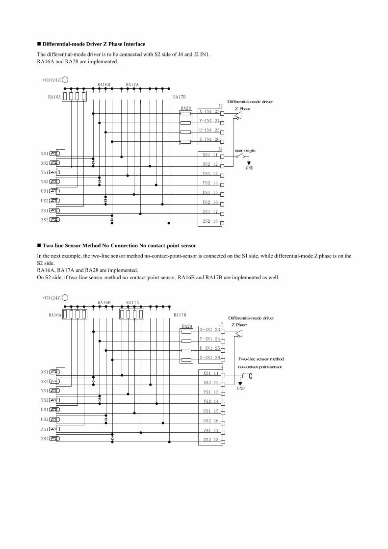
Differential-mode Driver Z Phase Interface
The differential-mode driver is to be connected with S2 side of J4 and J2 IN1. RA16A and RA28 are implemented.
GND
near origin
Z Phase
XS1
XS2
YS1
YS2
US1
US2
ZS1
ZS2
XS1 11
XS2 12
YS1 13
YS2 14
US1 15
US2 16
ZS1 17
ZS2 18
X-IN1 23
Y-IN1 24
U-IN1 25
Z-IN1 26
J2
J4
RA28
RA17B
RA17ARA16B
RA16A
+CD(24V)
Differential-mode driver
Two-line Sensor Method No-Connection No-contact-point-sensor
In the next example, the two-line sensor method no-contact-point-sensor is connected on the S1 side, while differential-mode Z phase is on the S2 side. RA16A, RA17A and RA28 are implemented. O n S2 side, if two-line sensor method no-contact-point-sensor, RA16B and RA17B are implemented as well.
GND
XS1
XS2
YS1
YS2
US1
US2
ZS1
ZS2
XS1 11
XS2 12
YS1 13
YS2 14
US1 15
US2 16
ZS1 17
ZS2 18
X-IN1 23
Y-IN1 24
U-IN1 25
Z-IN1 26
J2
J4
RA28
RA17B
RA17ARA16B
RA16A
+CD(24V)
Z PhaseDifferential-mode driver
Two-line sensor method
no-contact-point-sensor

MOP-096 96-point Output Board
Specification I/O 96-point photo-coupler isolated TR open collector output Control current Maximum 100 mA / 1 output power supply DC12~24V(I/O start up) (When DC 5V, 50 mA sink) consumption current DC5V 200mA(When all output is ON) (provided from bus) Operating temperature 0~50°C
Hardware Configuration
MOP-096 CEP-092AACCEL CORP.
J3
J5
J1
J4
J2
LED0~3LED4
DSW1
Accessories:
Power connector (H4P-SHF-AA) JST * 1 J5 Contact (BHF-001T-0.8SS) JST *4 J5
Mounted connectors
J1, 2 HIF-3B-26PA-2.54DS Hirose J3, 4 HIF-3B-26PA-2.54WB Hirose J5 BS4P-SHF-1AA JST
J1,2,3,4 Output Port In the case that DSW is 0, the port number allotted to J3 is 0~23, to J4 24~47, to J1 48~71 and to J2 72~95.
J5 I/O start up power supply DSW1 board address setting (one of 0, 1, 4 and 5) TR RN1423 (Toshiba) is used. LED0~3(Red) At RESET time, LED0 and LED is lightning.
At operation, the lower 4-bit written most lately is displayed. (Only for verification of operation) L ED4(Green) Power supply display LED.
Output Circuit Diagram
To the interiorPhotp coupler Output pin
2.2KR6.8K
J5-1,2
4.7K
RN1423
J1,2,3,4 +DC
J1,2,3,4
J5-3,4 RTN
Setting and Pin Assignment
J5 power supply Connector
On the RTN, sink current is gathered. Attention should be paid to the volume and be sure to use both two terminals.

Address Setting and Output Port
DSW1 IO J3,J4 J1,J2
0 0~95 MOP-048 #1 MOP-048 #21 96~191 MOP-048 #3 MOP-048 #44 384~479 MOP-048 #5 MOP-048 #65 480~575 MOP-048 #7 MOP-048 #8
*For details, refer the port number table of MOP-048.
J3 Output Port(upper) J1 Output Port(lower)
For output connector, white triangle on the connector is number 1, while component side is odd numbers and solder side is even
umbers. n Number 25 and 26 pin are equivalent of J5+DC and RTN respectively.
J4 Output Port(upper) J2 Output Port(lower)
* OFSET compatibilty is shown as below.
DSW=0 OFSET=0 DSW=1 OFSET=96 DSW=4 OFSET=384 DSW=5 OFSET=480
Output Equipment Connection Example
CR
LED R
SOL + -
+ -
J5
J1,J3
J2,J4
MOP-096
A K LED
Solenoid valve
Relay
Output control current is 100 mA maximum, and as solenoid valve and relay, those with a diode are used.
+DCPower supply
GND
12
34
JST

MOP-048 48-Point Output Board
Specification I/O 48-point photo-coupler isolated TR open collector output Control current Maximum 100 mA / 1 output Power supply DC 5~24 V (for driving the I/O) Consumed current DC 5V 80 mA (supplied from the bus) Operating temperature 0~50°C
Hardware Construction
MOP-048
ACCEL CORPCEP-013B
J3
J4
J5
LED TRアレイ
DIP2
Accessories: Power connector (H4P-SHF-AA) JST * 1 J5 Contact (BHF-001T-0.8SS) JST * 4 J5
Mounted connectors
J3, 4 HIF-3BA-26PA-2.54DS Hirose J5 BS4P-SHF-1AA JST
J3, 4 Output port When the board is #1, the port numbers become 0~23 for J3 and 24~47 for J4. Also, boards #1~4 have 0~191, and boards #5~8 have 384~575. As solenoids and relays, please use those with a surge-killer diode.
J5 I/O-driving power supply Current is concentrated to RTN. Please pay attention to the capacity of wire material.
LED1~24 Output monitor Indicates ON/OFF of the primary side (bus side) of the photocoupler. When the LED is on and the output does not operate, it is possible that the transistor array is damaged.
DIP2 Board address setting At ship-out time, A7~3 are ON.
TR array Output stage is TD62004, using four chips each.
Output Circuit Diagram
To the interior Photocoupler
TD62004 Display LED
2.2KR J5-1,2
J3,4-25 +DC
J3,4 Output pin
J5-3.4 RTN

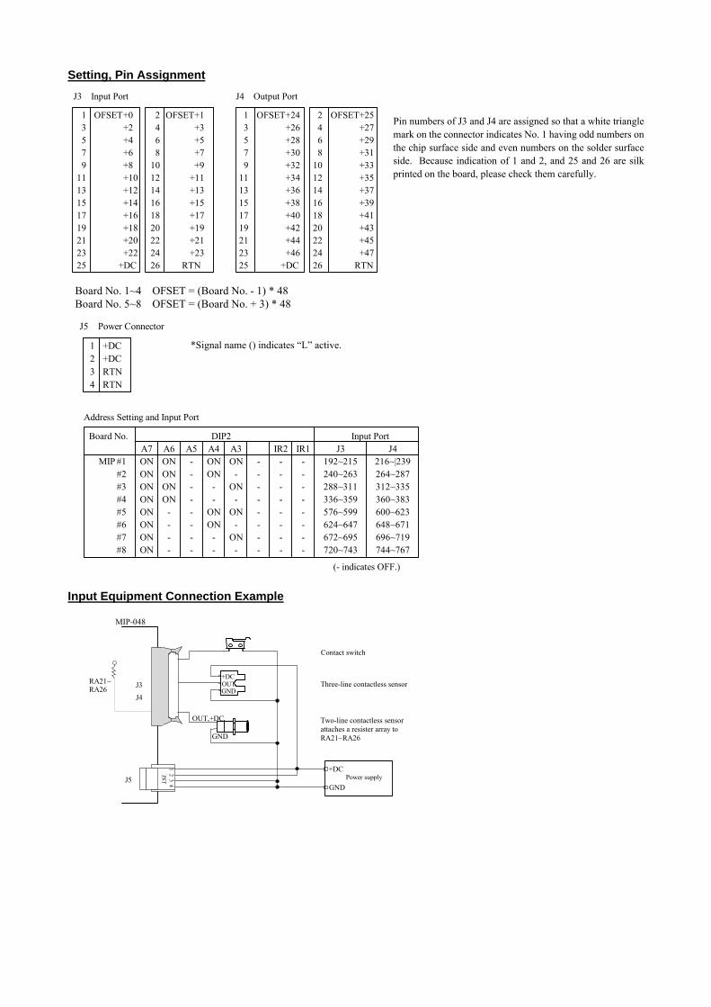
Setting, Pin Assignment J3 Input Port J4 Output Port
1 OFSET+0 2 OFSET+1 1 OFSET+24 2 OFSET+25 3 +2 4 +3 3 +26 4 +27 5 +4 6 +5 5 +28 6 +29 7 +6 8 +7 7 +30 8 +31 9 +8 10 +9 9 +32 10 +33 11 +10 12 +11 11 +34 12 +35 13 +12 14 +13 13 +36 14 +37 15 +14 16 +15 15 +38 16 +39 17 +16 18 +17 17 +40 18 +41 19 +18 20 +19 19 +42 20 +43 21 +20 22 +21 21 +44 22 +45 23 +22 24 +23 23 +46 24 +47 25 +DC 26 RTN 25 +DC 26 RTN
Board No. 1~4 OFSET = (Board No. - 1) * 48
Board No. 5~8 OFSET = (Board No. + 3) * 48
Pin numbers of J3 and J4 are assigned so that a white triangle mark on the connector indicates No. 1 having odd numbers on the chip surface side and even numbers on the solder surface side. Because indication of 1 and 2, and 25 and 26 are silk printed on the board, please check them carefully.
J5 Power Connector
1 +DC 2 +DC 3 RTN 4 RTN
*Signal name () indicates “L” active.
Address Setting and Output Port
Board No. DIP2 Output Port A7 A6 A5 A4 A3 IR2 IR1 J3 J4 MOP #1 ON ON ON ON ON - - - 0~ 23 24~ 47
#2 ON ON ON ON - - - - 48~ 71 72~ 95 #3 ON ON ON - ON - - - 96~119 120~143 #4 ON ON ON - - - - - 144~167 168~191 #5 ON - ON ON ON - - - 384~407 408~431 #6 ON - ON ON - - - - 432~455 456~479 #7 ON - ON - ON - - - 480~503 504~527 #8 ON - ON - - - - - 528~551 552~575
(- indicates OFF.)
Output Equipment Connection Example
CR
LED R
SOL + -
+ -
J5
J3
J4
MOP-048
A K LED
Solenoid valve
Relay
Output control current is 100 mA maximum, and as solenoid valve and relay, those with a diode are used.
+DCPower supply
GND
12
34
JST

MOP-048 Port Number Table
Conne Board Number / Bank Number / Port Numberctor
Pin #1 #2 #3 #4 #5 #6 #7 #8 1 0 48 96 144 384 432 480 528 2 1 49 97 145 385 433 481 529 3 2 50 98 146 386 434 482 530 4 0 3 51 99 147 387 435 483 531 5 4 52 100 148 388 436 484 532 6 5 53 101 149 389 437 485 533 7 6 54 102 150 390 438 486 534 8 7 55 103 151 391 439 487 535 9 8 56 104 152 392 440 488 536 10 9 57 105 153 393 441 489 537 11 10 58 106 154 394 442 490 538 12 1 11 59 107 155 395 443 491 539 13 12 60 108 156 396 444 492 540 14 13 61 109 157 397 445 493 541 15 14 62 110 158 398 446 494 542 16 15 63 111 159 399 447 495 543 17 16 64 112 160 400 448 496 544 18 17 65 113 161 401 449 497 545 19 18 66 114 162 402 450 498 546 20 2 19 67 115 163 403 451 499 547 21 20 68 116 164 404 452 500 548 22 21 69 117 165 405 453 501 549 23 22 70 118 166 406 454 502 550 24 23 71 119 167 407 455 503 551 1 24 72 120 168 408 456 504 552 2 25 73 121 169 409 457 505 553 3 26 74 122 170 410 458 506 554 4 3 27 75 123 171 411 459 507 555 5 28 76 124 172 412 460 508 556 6 29 77 125 173 413 461 509 557 7 30 78 126 174 414 462 510 558 8 31 79 127 175 415 463 511 559 9 32 80 128 176 416 464 512 560 10 33 81 129 177 417 465 513 561 11 34 82 130 178 418 466 514 562 12 4 35 83 131 179 419 467 515 563 13 36 84 132 180 420 468 516 564 14 37 85 133 181 421 469 517 565 15 38 86 134 182 422 470 518 566 16 39 87 135 183 423 471 519 567 17 40 88 136 184 424 472 520 568 18 41 89 137 185 425 473 521 569 19 42 90 138 186 426 474 522 570 20 5 43 91 139 187 427 475 523 571 21 44 92 140 188 428 476 524 572 22 45 93 141 189 429 477 525 573 23 46 94 142 190 430 478 526 574 24 47 95 143 191 431 479 527 575
Output
Input
12 18 48 54 60 66
J3
J4
13 19 49 55 61 67
14 20 50 56 62 68
15 21 51 57 63 69
10 16 22 52 58 64 70
17 23 53 59 65 7111
9
8
7
6
DIP2 setting
ON
1 2 3 4 5 6 7 8
#1
ON
1 2 3 4 5 6 7 8
#2
ON
1 2 3 4 5 6 7 8
#3
ON
1 2 3 4 5 6 7 8
#4
ON
1 2 3 4 5 6 7 8
#5
ON
1 2 3 4 5 6 7 8
#6
ON
1 2 3 4 5 6 7 8
#7
ON
1 2 3 4 5 6 7 8
#8
Port numbers are expressed in 1 bit unit and bank numbers in 8 bit unit. In the ON/OFF command, ON/OFF of 1 bit at a time is done by specifying a port number as a parameter. In the OUT command, ON/OFF of 8 bits at a time is done by specifying a bank number.

MIP-096 96-point Input Board
Specification I/O 96-point photo-coupler isolated TR open collector input Control current About 3.5 mA / 1 input Power supply DC (5)12~24 V (for driving the I/O) Consumed current DC 5V 100 mA (supplied from the bus) Operating temperature 0~50°C
Hardware Configuration Accessories:
Power connector (H4P-SHF-AA) JST * 1 J5 Contact (BHF-001T-0.8SS) JST * 4 J5
Mounted connectors
J3, 4 J3429-P302VE Hirose J5 BS4P-SHF-1AA JST
J3, 4 Input port In the case that DSW is 2, the port number allotted to J3 is 192~215, to J4 216~239, to J1 240~263 and to J2 264~287.
J5 I/O-driving power supply LED0~3(green) Input port display LED4(Green) Power supply display LED. RA0~11 Two-line sensor method sensor compatible SIP socket array DSW1 Selector of board. Choose one of 2, 3, 6 and 7. DSW2,DP1 Selector of Input port display. Port display selector.
Input Circuit Diagram socket for a two-line contactless sensor pull-up resister
TLP181
RT+DC
J5
J3,J4(J1,J2)
Input connector
Power connector
To the interior
1~24
1,2
3,4
IN
6.8 *1
Connector / Pin Socket Connector / Pin Socket J3 1~8 RA0 (J1) 1~8 RA6 J3 9~16 RA1 (J1) 9~16 RA7 J3 17~24 RA2 (J1) 17~24 RA8 J4 1~8 RA3 (J2) 1~8 RA9 J4 9~16 RA4 (J2) 9~16 RA10 J4 17~24 RA5 (J2 )17~24 RA11
*At the ship-out time, only a socket for a two-line contactless sensor pull-up resister is mounted. When using a two-line contactless sensor, please mount a BH9-1-272G equivalent one.

Setting and Pin Assignment
J3 Input Port (upper) J1 Input Port (lower)
For the input connector, the white triangle on the connector is number 1, while component side is odd numbers and solder side
even numbers. is Number 25 and 26 pin are equivalent of J5+DC and RTN respectively.
J4 Input Port (upper) J2 Input Port (lower)
* OFSET compatibility is shown as below.
*According to the settings of DSW2 and DP1, LED1~3 are set to following port display. DSW2 select bank (every 8 bits) and DP1-1 selects lower 4-bit and upper 4-bit.
DSW2 Connector DP1-1 ON DP1 1 OFF -0 J3 1~4 5~8 1 J3 9~12 13~16 2 J3 17~20 21~24 3 J4 1~4 5~8 4 J4 9~12 13~16 5 J4 17~20 21~24 6 (J1) 1~4 5~8 7 (J1) 9~12 13~16 8 (J1) 17~20 21~24 9 (J2) 1~4 5~8 A (J2) 9~12 13~16 B (J2) 17~20 21~24

J5 Power Supply Connector Address Setting(DSW1) and Input Port
1 +DC 2 +DC 3 RTN 4 RTN
DSW1 IO J3,J4 (J1,J2) 2 192~287 MIP-048 #1 MIP-048 #23 288~383 MIP-048 #3 MIP-048 #46 576~671 MIP-048 #5 MIP-048 #67 672~767 MIP-048 #7 MIP-048 #8
*For pin assignment and input numbers, refer to “MIP-048 Port Number Table”.
Output Equipment Connection Example
J5
J1 J3
J2 J4
MIP-096
Contact switch
+DC OUT GND
OUT,+DC
GND
Power supply +DC
GND
Three-line contactless sensor
Two-line contactless sensor attaches a resister array to RA0~RA11
6.8K
1 23 4
JST

MIP-048 48-Point Input Board
Specification I/O 48-point photo-coupler isolated input Input current About 2 mA / 1 input Power supply DC (5)12~24 V (for driving the I/O) Consumed current DC 5V 30 mA (supplied from the bus) Operating temperature 0~50°C
Hardware Construction
CEP-012BMIP-048 REV-2.00
J3
J5
LED
J4
SIP socket for attaching a resister array for dealing with a sensor
Accessories: (1) Power connector (H4P-SHF-AA) JST *1 J5 (2) Contact (BHF-001T-0.8SS) JST *4 J5
Mounted connectors
J3, 4 HIF-3BA-26PA-2.54DS Hirose J5 BS4P-SHF-1AA JST
J3, 4 Input port When the board is #1, the port numbers become 192~215 for J3 and 216~239 for J4. Also, boards #1~4 have 192~383, and boards #5~8 have 576~767.
J5 I/O-driving power supply LED1~24 Input monitor
Indicates ON/OFF of the secondary side (connector side) of the photocoupler. DIP2 Board address setting
IR1 Hands over an interrupt input to the CPU board (J4-1 input). IR2 Hands over an interrupt input to the CPU board (J4-2 input).
RA9~20 Input current limiting resister array When using the I/O interface power supply at 5 V, the resister array should be replaced (6.8 kΩ standard).
RA21~26 An SIP socket for mounting a resister array to deal with two-line contactless sensor.
Input Circuit Diagram
TLP521
RT+DC
J5
J3,J4
Input connector
Power connector
Input display
To the interior
1~24
1,2
3,4
IN
*1 *2
*1 RAD is replaceable with the SIP socket (6.8 KΩ standard). *2 At the ship-out time, only a socket for a two-line contactless sensor pull-up resister is mounted.
When using a two-line contactless sensor, please mount a BH9-1-272G equivalent one.
Setting, Pin Assignment J3 Input Port J4 Output Port
1 OFSET +0 2 OFSET+1 1 OFSET+24 2 OFSET+25 3 +2 4 +3 3 +26 4 +27 5 +4 6 +5 5 +28 6 +29 7 +6 8 +7 7 +30 8 +31 9 +8 10 +9 9 +32 10 +33 11 +10 12 +11 11 +34 12 +35 13 +12 14 +13 13 +36 14 +37 15 +14 16 +15 15 +38 16 +39 17 +16 18 +17 17 +40 18 +41 19 +18 20 +19 19 +42 20 +43 21 +20 22 +21 21 +44 22 +45 23 +22 24 +23 23 +46 24 +47 25 +DC 26 RTN 25 +DC 26 RTN Board No. 1~4 OFSET = (Board No. - 1) * 48 Board No. 5~8 OFSET = (Board No. + 3) * 48
Pin numbers of J3 and J4 are assigned so that a white triangle mark on the connector indicates No. 1 having odd numbers on the chip surface side and even numbers on the solder surface side. Because indication of 1 and 2, and 25 and 26 are silk printed on the board, please check them carefully.
J5 Power Connector
1 +DC 2 +DC 3 RTN 4 RTN
*Signal name () indicates “L” active.
Address Setting and Input Port
Board No. DIP2 Input Port A7 A6 A5 A4 A3 IR2 IR1 J3 J4 MIP #1 ON ON - ON ON - - - 192~215 216~|239 #2 ON ON - ON - - - - 240~263 264~287 #3 ON ON - - ON - - - 288~311 312~335 #4 ON ON - - - - - - 336~359 360~383 #5 ON - - ON ON - - - 576~599 600~623 #6 ON - - ON - - - - 624~647 648~671 #7 ON - - - ON - - - 672~695 696~719 #8 ON - - - - - - - 720~743 744~767
(- indicates OFF.)
Input Equipment Connection Example
J5
J3
J4
MIP-048
Contact switch
+DCOUTGND
OUT,+DC
GND
Power supply+DC
GND
Three-line contactless sensor
Two-line contactless sensorattaches a resister array toRA21~RA26
RA21~RA26
12
34
JST
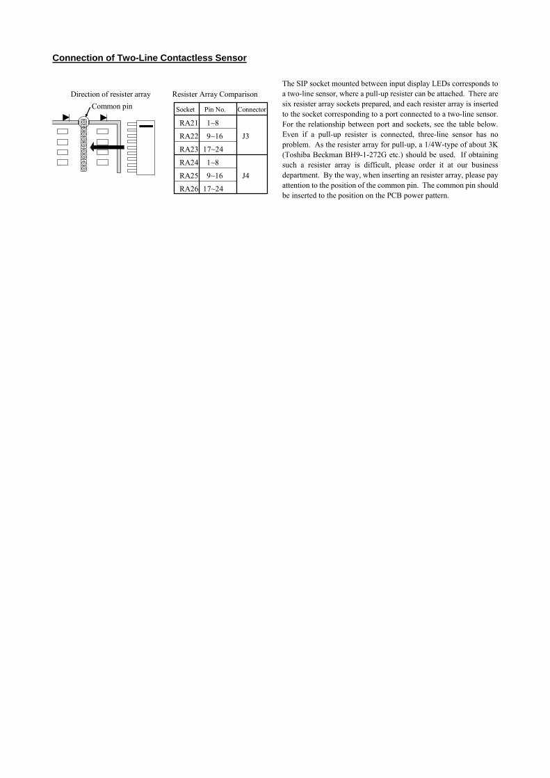
Connection of Two-Line Contactless Sensor The SIP socket mounted between input display LEDs corresponds to a two-line sensor, where a pull-up resister can be attached. There are six resister array sockets prepared, and each resister array is inserted to the socket corresponding to a port connected to a two-line sensor. For the relationship between port and sockets, see the table below. Even if a pull-up resister is connected, three-line sensor has no problem. As the resister array for pull-up, a 1/4W-type of about 3K (Toshiba Beckman BH9-1-272G etc.) should be used. If obtaining such a resister array is difficult, please order it at our business department. By the way, when inserting an resister array, please pay attention to the position of the common pin. The common pin should be inserted to the position on the PCB power pattern.
Socket Pin No. Connector
RA21 1~8
RA22 9~16 J3
RA23 17~24
RA24 1~8
RA25 9~16 J4
RA26 17~24
Resister Array ComparisonDirection of resister array Common pin

MIP-048 Port Number Table
Conne Board Number / Bank Number / Port Numberctor
Pin #1 #2 #3 #4 #5 #6 #7 #8 1 192 240 288 336 576 624 672 720 2 193 241 289 337 577 625 673 721 3 194 242 290 338 578 626 674 722 4 195 243 291 339 579 627 675 723 5 196 244 292 340 580 628 676 724 6 197 245 293 341 581 629 677 725 7 198 246 294 342 582 630 678 726 8 199 247 295 343 583 631 679 727 9 200 248 296 344 584 632 680 728 10 201 249 297 345 585 633 681 729 11 202 250 298 346 586 634 682 730 12 203 251 299 347 587 635 683 731 13 204 252 300 348 588 636 684 732 14 205 253 301 349 589 637 685 733 15 206 254 302 350 590 638 686 734 16 207 255 303 351 591 639 687 735 17 208 256 304 352 592 640 688 736 18 209 257 305 353 593 641 689 737 19 210 258 306 354 594 642 690 738 20 211 259 307 355 595 643 691 739 21 212 260 308 356 596 644 692 740 22 213 261 309 357 597 645 693 741 23 214 262 310 358 598 646 694 742 24 215 263 311 359 599 647 695 743 1 216 264 312 360 600 648 696 744 2 217 265 313 361 601 649 697 745 3 218 266 314 362 602 650 698 746 4 219 267 315 363 603 651 699 747 5 220 268 316 364 604 652 700 748 6 221 269 317 365 605 653 701 749 7 222 270 318 366 606 654 702 750 8 223 271 319 367 607 655 703 751 9 224 272 320 368 608 656 704 752 10 225 273 321 369 609 657 705 753 11 226 274 322 370 610 658 706 754 12 227 275 323 371 611 659 707 755 13 228 276 324 372 612 660 708 756 14 229 277 325 373 613 661 709 757 15 230 278 326 374 614 662 710 758 16 231 279 327 375 615 663 711 759 17 232 280 328 376 616 664 712 760 18 233 281 329 377 617 665 713 761 19 234 282 330 378 618 666 714 762 20 235 283 331 379 619 667 715 763 21 236 284 332 380 620 668 716 764 22 237 285 333 381 621 669 717 765 23 238 286 334 382 622 670 718 766 24 239 287 335 383 623 671 719 767
36 42 72 78 84 90
J3
J4
37 43 73 79 85 91
38 44 74 80 86 92
39 45 75 81 87 93
34 40 46 76 82 88 94
41 47 77 83 89 9535
33
32
31
30
28
29
27
26
25
24
DIP2 setting
ON
1 2 3 4 5 6 7 8
#1
ON
1 2 3 4 5 6 7 8
#2
ON#3
ON
1 2 3 4 5 6 7 8
#4
ON
1 2 3 4 5 6 7 8
#5
ON
1 2 3 4 5 6 7 8
#6
ON
1 2 3 4 5 6 7 8
#7
ON
1 2 3 4 5 6 7 8
#8
1 2 3 4 5 6 7 8
Port numbers are expressed in 1 bit unit and bank numbers in 8 bit unit. In the SW() function, input is done by 1 bit at a time by specifying a port number as a parameter. In the IN() command, 8 bits are input at once by specifying a bank number.

IOP-048 24-Point Input and 24-Point Output Board
Specification I/O 24-point photo-coupler isolated input 24-point photo-coupler isolated TR open collector output Output control current Maximum 100 mA / 1 output Input current About 2 mA / 1 input Power supply DC (5)12~24 V (for driving the I/O) Consumed current DC 5V 50 mA (supplied from the bus) Operating temperature 0~50°C
Hardware Construction
A C C E L C O R P . C E P - 0 3 7 R E V - 1 . 0 0 I O P - 0 4 8
J3
J4
J5
LED (Red)
DIP2
SIP socket for attaching a resister array for dealing with a contactless 2-line sensor
TR array
LED (Green)
Accessories:
(1) Power connector (H4P-SHF-AA) JST *1 J5 (2) Contact (BHF-001T-0.8SS) JST *4 J5
Mounted connectors
J3, 4 HIF-3BA-26PA-2.54DS Hirose J5 BS4P-SHF-1AA JST
J3 Output port J4 Input port
IOP-048 inherits MOP-048. The port numbers are in the same arrangement with MOP, the first 24 ports being output, the latter 24 ports being input.
J5 I/O-driving power supply LED1~24 (Red) Output monitor
Indicates ON/OFF of the primary side (bus side) of the photocoupler. If LED is on and output does not function, it is possible that the transistor array is damaged.
LED1~24 (Green) Input monitor Indicates ON/OFF of the secondary side (connector side) of the photocoupler.
DIP2 Board address setting The same address with MOP. Please set it so that it does not overlap with MOP. A7~3 are ON when shipped out.
RA15~20 Input current limiting resister array When using the I/O interface power supply at 5 V, the resister array should be replaced (6.8 kΩ standard).
RA24~26 An SIP socket for mounting a resister array to deal with two-line contactless sensor. TR array Output stage is TD62004, using four chips each.
Input Circuit Diagram Input circuit is equivalent with MIP-048, and output circuit with MIP-048.

Setting, Pin Assignment J3 Output Port J4 Input Port
1 OFSET +0 2 OFSET +1 1 OFSET+24 2 OFSET+25 3 +2 4 +3 3 +26 4 +27 5 +4 6 +5 5 +28 6 +29 7 +6 8 +7 7 +30 8 +31 9 +8 10 +9 9 +32 10 +33 11 +10 12 +11 11 +34 12 +35 13 +12 14 +13 13 +36 14 +37 15 +14 16 +15 15 +38 16 +39 17 +16 18 +17 17 +40 18 +41 19 +18 20 +19 19 +42 20 +43 21 +20 22 +21 21 +44 22 +45 23 +22 24 +23 23 +46 24 +47 25 +DC 26 RTN 25 +DC 26 RTN
Board No. 1~4 OFSET = (Board No. - 1) * 48 Board No. 5~8 OFSET = (Board No. + 3) * 48
Pin numbers of J3 and J4 are assigned so that a white triangle mark on the connector indicates No. 1 having odd numbers on the chip surface side and even numbers on the solder surface side. Because indication of 1 and 2, and 25 and 26 are silk printed on the board, please check them carefully.
*Signal name () indicates “L” active. J5 Power Connector
1 +DC 2 +DC 3 RTN 4 RTN
Address Setting and Input Port
Board No. DIP2 J3 J4 A7 A6 A5 A4 A3 IR2 IR1 Output Input MOP #1 ON ON ON ON ON - - - 0~ 23 24~ 47
#2 ON ON ON ON - - - - 48~ 71 72~ 95 #3 ON ON ON - ON - - - 96~119 120~143 #4 ON ON ON - - - - - 144~167 168~191 #5 ON - ON ON ON - - - 384~407 408~431 #6 ON - ON ON - - - - 432~455 456~479 #7 ON - ON - ON - - - 480~503 504~527 #8 ON - ON - - - - - 528~551 552~575
(- indicates OFF.)

IOP-048 Port Number Table
Conne Board Number / Bank Number / Port Numberctor
Pin #1 #2 #3 #4 #5 #6 #7 #8 1 0 48 96 144 384 432 480 528 2 1 49 97 145 385 433 481 529 3 2 50 98 146 386 434 482 530 4 0 3 51 99 147 387 435 483 531 5 4 52 100 148 388 436 484 532 6 5 53 101 149 389 437 485 533 7 6 54 102 150 390 438 486 534 8 7 55 103 151 391 439 487 535 9 8 56 104 152 392 440 488 536 10 9 57 105 153 393 441 489 537 11 10 58 106 154 394 442 490 538 12 1 11 59 107 155 395 443 491 539 13 12 60 108 156 396 444 492 540 14 13 61 109 157 397 445 493 541 15 14 62 110 158 398 446 494 542 16 15 63 111 159 399 447 495 543 17 16 64 112 160 400 448 496 544 18 17 65 113 161 401 449 497 545 19 18 66 114 162 402 450 498 546 20 2 19 67 115 163 403 451 499 547 21 20 68 116 164 404 452 500 548 22 21 69 117 165 405 453 501 549 23 22 70 118 166 406 454 502 550 24 23 71 119 167 407 455 503 551 1 24 72 120 168 408 456 504 552 2 25 73 121 169 409 457 505 553 3 26 74 122 170 410 458 506 554 4 3 27 75 123 171 411 459 507 555 5 28 76 124 172 412 460 508 556 6 29 77 125 173 413 461 509 557 7 30 78 126 174 414 462 510 558 8 31 79 127 175 415 463 511 559 9 32 80 128 176 416 464 512 560 10 33 81 129 177 417 465 513 561 11 34 82 130 178 418 466 514 562 12 4 35 83 131 179 419 467 515 563 13 36 84 132 180 420 468 516 564 14 37 85 133 181 421 469 517 565 15 38 86 134 182 422 470 518 566 16 39 87 135 183 423 471 519 567 17 40 88 136 184 424 472 520 568 18 41 89 137 185 425 473 521 569 19 42 90 138 186 426 474 522 570 20 5 43 91 139 187 427 475 523 571 21 44 92 140 188 428 476 524 572 22 45 93 141 189 429 477 525 573 23 46 94 142 190 430 478 526 574 24 47 95 143 191 431 479 527 575
Output
Input
12 18 48 54 60 66
J3
J4
13 19 49 55 61 67
14 20 50 56 62 68
15 21 51 57 63 69
10 16 22 52 58 64 70
17 23 53 59 65 7111
9
8
7
6
DIP2 setting
ON
1 2 3 4 5 6 7 8
#1
ON
1 2 3 4 5 6 7 8
#2
ON
1 2 3 4 5 6 7 8
#3
ON
1 2 3 4 5 6 7 8
#4
ON
1 2 3 4 5 6 7 8
#5
ON
1 2 3 4 5 6 7 8
#6
ON
1 2 3 4 5 6 7 8
#7
ON
1 2 3 4 5 6 7 8
#8

MPG-3202 S-Shape Compatible PG & Encoder Counter Board
Specification (* indicates per one X3202) PG IC X3202: 2 pieces Pulse generation* 1-axis differential output Maximum 1 Mpps ~ Minimum 0.1 pps Z-phase input* 1 channel Encoder input* 1 channel 2 clock, 90° phase difference 2-phase clock 1,2,4 times Input* Origin sensor, driver alarm, etc. (Total 8 points) Output* Servo on, servo driver variation counter clear, etc. (Total 4 points) Number of supported MPCs 8 pieces (16 axes) Power supply DC 12~24 V (for driving the I/O) Consumed current DC 5V 200 mA.(supplied from the bus) Operating temperature 0~50°C
Hardware Construction
MPG-3202 EP-075BACCEL CORP.
LED1,2
LED22
LED13*20
LED11,12
J1
J2
J3
RA
13R
A16
LED3*10
RA
11R
A15
U2
U3
DSW1
Accessories:
(1) Power connector (H4P-SHF-AA) JST *1 J3 (2) Contact (BHF-001T-0.8SS) JST *4 J3
Mounted connectors
J1, J2 HIF-3BA-26PA-2.54DS Hirose J3 BS4P-SHF-1AA JST
J1, 2 Pulse output, Z-phase input, encoder input, other I/Os J3 I/O driving power RA11, RA15 Shunt resister for sensor input. Please change upon necessity. At factory ship-out, 6.8 KΩ is inserted. RA13, RA16 An SIP socket compatible with a two-line sensor containing an amplifier. When using it, please insert a
resister array of about 2.7 KΩ 1/4 W. LED22 Power supply monitor LED1,2,11,12 Pulse output monitor LED3~10,13~20 Input monitor LED3,13 ORGI LED4,14 ALM LED5,15 +SLD LED6,16 -SLD LED7,17 INP LED8,18 MARK LED9,19 +EL LED10,20 -EL DSW1 Board address setting (Odd numbers only from 1)
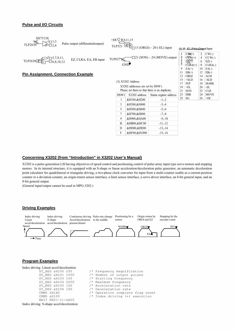
Pulse and I/O Circuits
Pin Assignment, Connection Example
SN75158
TLP2630
TLP521
+DC RA11,15
TLP627
GND
Pulse output (differentialoutput)
EZ, CLRA, EA, EB input
13 (ORGI) ~ 20 (-EL) input
+ - TLP2630
+ -
1,3
21 (SON) ~ 24 (MOVE) output
2,4
5,7,9,11, 6,8,10,12
(1) J1, J2 Pulse Output/Input
1 CW(+) 2 CW(-) 3 CCW(+) 4 CCW(-) 5 EZ(+) 6 EZ(-) 7 CLRA(+) 8 CLRA(-) 9 EA(+) 10 EA(-) 11 EB(+) 12 EB(-) 13 ORGI 14 ALM 15 +SLD 16 -SLD 17 INP 18 MARK 19 +EL 20 -EL 21 SON 22 CLR 23 ERR 24 MOVE 25 SG 26 +DC
(2) J3 Power Connector
1 2 3 4
+DC NC GND FG
(3) X3202 Address X3202 addresses are set by DSW1. Please set them so that there is no duplicate.DSW1 X3202 address Status register address
1 &H100,&H200 -1,-23 &H300,&H400 -3,-45 &H500,&H600 -5,-67 &H700,&H800 -7,-89 &H900,&HA00 -9,-10B &HB00,&HC00 -11,-12D &HD00,&HE00 -13,-14F &HF00,&H1000 -15,-16
Concerning X3202 (from “Introduction” in X3202 User’s Manual) X3202 is a pulse-generation LSI having objectives of speed control and positioning control of pulse-array input type servo motors and stepping motors. In its internal structure, it is equipped with an S-shape or linear acceleration/deceleration pulse generator, an automatic deceleration point calculator for quadrilateral or triangular driving, a two-phase clock converter for input from a multi-counter usable as a current-position counter or a deviation counter, an origin-return sensor interface, a limit sensor interface, a servo driver interface, an 8-bit general input, and an 8-bit general output. (General input/output cannot be used in MPG-3202.)
Driving Examples
MARK
Index driving Linear accel/deceleration
EZ
ORGI INT
Time
Speed
Index driving S-shape accel/deceleration
Continuous driving Accel/deceleration present/absent
Pulse rate change in the middle
Positioning by a sensor
Origin return by ORGI and EZ
Stopping by the encoder count
Program Examples Index driving Linear accel/deceleration
ST_REG &H100 250 /* Frequency magnification ST_REG &H101 1000 /* Number of output pulses ST_REG &H103 100 /* Starting frequency ST_REG &H104 2000 /* Maximum frequency ST_REG &H105 100 /* Acceleration rate ST_REG &H106 100 /* Deceleration rate CMND &H1A0 /* Operation complete flag reset CMND &H100 /* Index driving (+) execution WAIT REG(-1)=&H20
Index driving S-shape accel/deceleration

ST_REG &H100 250 /* Frequency magnification ST_REG &H101 1000 /* Number of output pulses ST_REG &H103 100 /* Starting frequency ST_REG &H104 2000 /* Acceleration rate ST_REG &H105 100 /* Deceleration rate ST_REG &H106 100 /* S-shape accel/deceleration section ST_REG &H107 2000 /* Operation mode = S-shape accel/deceration mode ST_REG &H160 &H10 /* Operation complete flag reset CMND &H1A0 /* Index driving (+) execution CMND &H100 WAIT REG(-1)=&H20
Continuous driving Pulse rate change in the middle
ST_REG &H100 250 /* Frequency magnification ST_REG &H103 100 /* Starting frequency ST_REG &H104 1000 /* Maximum frequency ST_REG &H105 100 /* Acceleration rate ST_REG &H106 100 /* Deceleration rate CMND &H1A0 /* Operation complete flag reset CMND &H106 /* Continuous driving (+) execution INPUT A /* FTM waiting for the Enter key ST_REG &H104 2000 /* Changing the maximum frequency INPUT A CMND &H131 /* Stop deceleration
Rotary encoder count
ST_REG &H151 &H03 /* Two-phase clock 1 multiplication ST_REG &H152 &H02 /* Counter A = Channel 1 CMND &H150 /* Operation complete flag reset DO E0=REG(&H121) */ Reading counter A IF E0&&H800000<>0 THEN E0=E0-&HFFFFFF END_IF PRINT E0 TIME 500 LOOP
[Cited references] Kyopal X3202 User’s Manual was referred to in making this document. [Detailed materials] Please see “MPG-3202 Detailed Manual” for connection examples, sample programs, and X3202
commands/registers.

MRS-402 RS-232C Expansion Board
Specification CPU KL5C80A ROM FR4M: 1 piece RAM HM62256PL-12 equivalent: 1 piece RS-232C Photo-coupler isolated 2 CH. RS-485 switchable. Input buffer 1K byte / 1CH Power supply DC 12~24 V Consumed current DC 5V, 50 mA.(supplied from the bus) Operating temperature 0~50°C
Hardware Construction
MRS-402 CEP-059BACCEL CORP.
J2
J1
J5
D4D3
D2D1
DSW1
DSW2
SP2SP3SP5
SP4
Accessories: (1) Power connector (H4P-SHF-AA) JST *1 J5 (2) Contact (BHF-001T-0.8SS) JST *4 J5
Mounted connectors
J1, J2 HIF-3BD-10PA-2.54DS Hirose J5 BS4P-SHF-1AA JST
J1, J2 RS-232C ports J5 I/F power supply D1, 3 (Red) Input buffer with characters D2 (Green) Power supply display D4 (Green) Operation display DSW1 Rotary switch for setting addresses DSW2 Rotary switch for maintenance SP2~5 Short pin for switching RS-232C/485
Setting
(2) RS-232C/485 SwitchingShort pin setting
RS-232C *1 RS-485
J1 SP4: 1-2 shorted SP2: Open
SP4: 1-3 shorted *2 SP2: Terminator *3
J2 SP5: 1-2 shorted SP3: Open
SP5: 1-3 shorted SP3: Terminator
*1 indicates the condition when shipped out of factory.*2 SP4,5: 1-3 short is done by breaking the pin 2 and usingthe short pin of SP2, 3.*3 Terminator ON of SP2, 3 is done using the 2P short pin ofSP4, 5.
(1) Board Address Setting and Channel NumbersBoard address DSW1 setting J1 channel J2 channel
1 9 3 42 8 5 63 7 7 8

Pin Assignment
(2) J5 Power Connector
1 +DC23 GND4 FG
(1) J1, J2 RS-232C Port 1 FG 2 TXD 3 RXD 4 RTS 5 CTS 6 NC 7 SG 8 DA 9 DB 10 DTR
* DB, DA indicate the case of SR-485.
*When 485 is used, 5-10 shorted.
Command Support Commands of MRS-402 are expanded commands of the standard port. Please specify the channel number set by DSW1 at the number portion of each command.
CNFG#n, INPUT#n, PRINT#n, INP$#n()¥, PUT#n, LOF(n), RSE(n) , RS n n = Channel number
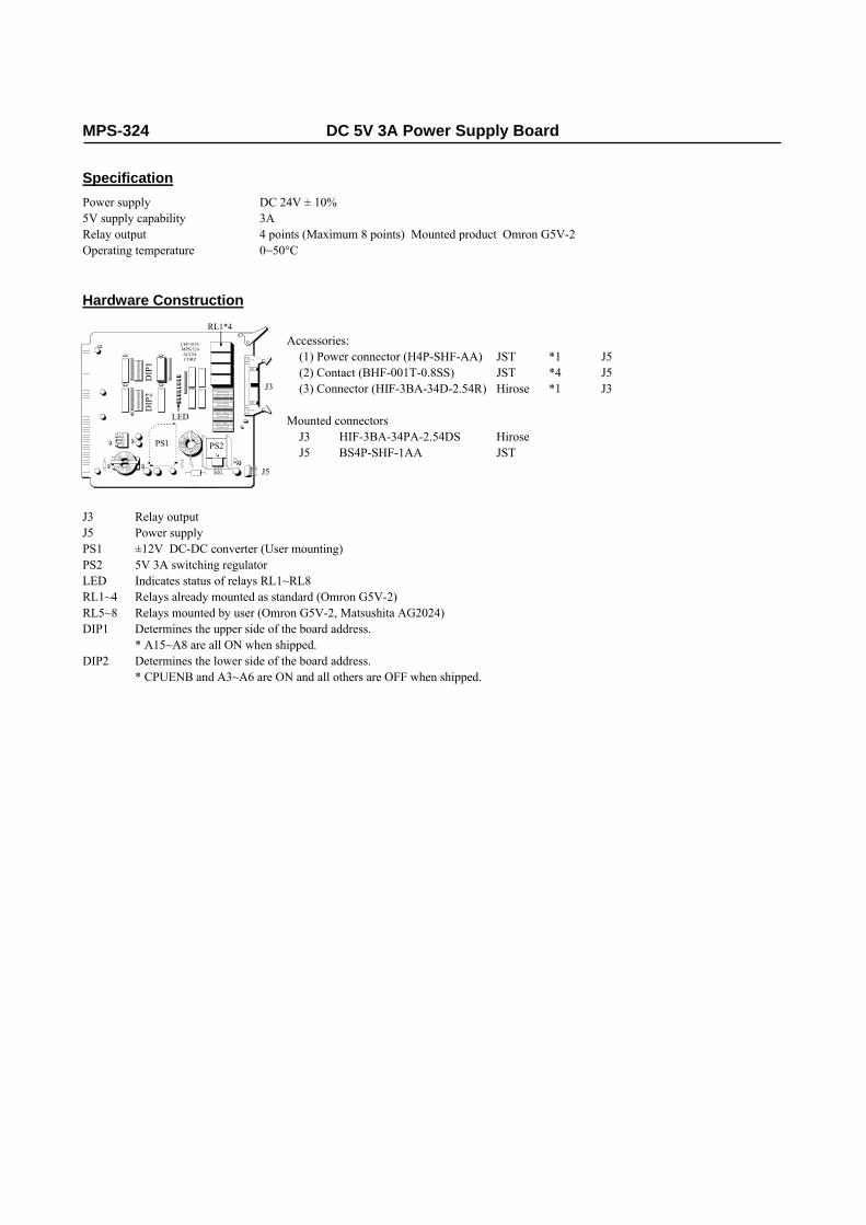
MPS-324 DC 5V 3A Power Supply Board
Specification Power supply DC 24V ± 10% 5V supply capability 3A Relay output 4 points (Maximum 8 points) Mounted product Omron G5V-2 Operating temperature 0~50°C
Hardware Construction
CEP-015CMPS-324ACCELCORP.
J3
J5
PS1 PS2
DIP
1D
IP2
RL1*4
LED
Accessories: (1) Power connector (H4P-SHF-AA) JST *1 J5 (2) Contact (BHF-001T-0.8SS) JST *4 J5 (3) Connector (HIF-3BA-34D-2.54R) Hirose *1 J3
Mounted connectors
J3 HIF-3BA-34PA-2.54DS Hirose J5 BS4P-SHF-1AA JST
J3 Relay output J5 Power supply PS1 ±12V DC-DC converter (User mounting) PS2 5V 3A switching regulator LED Indicates status of relays RL1~RL8 RL1~4 Relays already mounted as standard (Omron G5V-2) RL5~8 Relays mounted by user (Omron G5V-2, Matsushita AG2024) DIP1 Determines the upper side of the board address. * A15~A8 are all ON when shipped. DIP2 Determines the lower side of the board address. * CPUENB and A3~A6 are ON and all others are OFF when shipped.
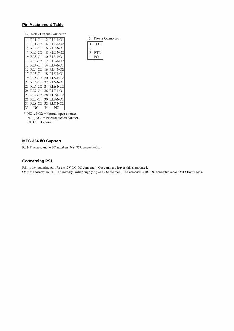
Pin Assignment Table
1 RL1-C1 2 RL1-NO1 3 RL1-C2 4 RL1-NO2 5 RL2-C1 6 RL2-NO1 7 RL2-C2 8 RL2-NO2 9 RL3-C1 10 RL3-NO1 11 RL3-C2 12 RL3-NO2 13 RL4-C1 14 RL4-NO1 15 RL4-C2 16 RL4-NO2 17 RL5-C1 18 RL5-NO1 19 RL5-C2 20 RL5-NC2 21 RL6-C1 22 RL6-NO1 23 RL6-C2 24 RL6-NC2 25 RL7-C1 26 RL7-NO1 27 RL7-C2 28 RL7-NC2 29 RL8-C1 30 RL8-NO1 31 RL8-C2 32 RL8-NC2 33 NC 34 NC
* NO1, NO2 = Normal open contact. NC1, NC2 = Normal closed contact. C1, C2 = Common
J3 Relay Output Connector
1 +DC 2 3 RTN 4 FG
J5 Power Connector
MPS-324 I/O Support RL1~8 correspond to I/O numbers 768~775, respectively.
Concerning PS1 PS1 is the mounting part for a ±12V DC-DC converter. Out company leaves this unmounted. Only the case where PS1 is necessary iswhen supplying ±12V to the rack. The compatible DC-DC converter is ZW32412 from Elcoh.

MPS-324 Connection Example
123456789
10111213141516171819202122232425262728293031323334
C1 NO1 C2
NO2 C1
NO1 C2
NO2 C1
NO1 C2
NO2 C1
NO1 C2
NO2 C1
NO1 C2
NC2 C1
NO1 C2
NC2 C1
NO1 C2
NC2 C1
NO1 C2
NC2
RL1
RL2
RL3
RL4
RL5
RL6
RL7
RL8
NC NC
234
1
(768)
(769)
(770)
(771)
(772)
(773)
(774)
(775)
+DC
GNDPower supply
CRCan be used for driving equipment such as relays and patrite whose control current exceed 100 mA or as an interface with external equipment.
IN
NO1,2
NC1,2
C1,2
J5
Normal open contact
Normal closed contact
Common
J3
IN Sequencer etc.
RL1~RL4 are already loaded when shipped, and RL5~RL8 are loaded by the user. Numbers inside () indicate port numbers in the ON/OFF command.

MBK-SH Touch Panel Interface
Specification CPU HITACH SH-2(HD64F7051F20) ROM FR8M(29F40*2) option RAM HM628128*2 DPM CY7C144-55JC*2 Communication Port User port RS-422/232 selection x 2 (one maintenance port) Display 7 segment x 6 Power supply DC 12~24 V Consumed current 300 mA.( DC 5V) Operating temperature 0~50°C Communication Protocol Panasonic MEWNET-FP Protocol-compliant, other sequencer upper link protocol (partial) User Memory Data area 7900 words, I/O area 100 words
Features ·Digital’s touch panel, GP series, can be connected with direct access method. ·Taking personal computer as upper order, MEWNET-FP protocol-compliant communication is available. (*1) ·With Omron sequencer and Mitsubishi sequencer, link connection can be established. (MBK is host.)(*1) ·It displays real time steps of execution process of the program. (*1) signifies the exclusive use.
Hardware Configuration
J1
J4
J5
J3
J2
S3S2S1
SP2,SP2A,SP1A
MBK-SH CEP-098BACCEL CORP.
MEMDSW1DSW2
SP1
Accessories: (1) Power connector (H4P-SHF-AA) JST *1 J3 (2) Contact (BHF-001T-0.8SS) JST *4 J3
Mounted connectors
J1 HIF-3FC-10PA-2.54DSA Hirose J2 HIF-3FC-10PA-2.54DS Hirose J4 BS4P-SHF-1AA JST J5 XW4A-02B1-H1 Omron
J1 Communication port for maintenance J2 Communication port. RS-422/232-selection. Protocol-selection. Connection with PC or sequencer. J3 Communication port. RS-422/232-selection. MEWNET-FP protocol 38400 bps fixed. For Digital touch panel connection. J4 For interface. Power supply (DC 12~24V). J5 External DC 5V supply. (Stop 5 V of MPC-684 to provide power from here.) SP1,SP1A J2 connector RS-422/232 switch SP2,SP2A J3 connector RS-422/232 switch DSW1 System selection. (9=internal ROM/A=FR8M(Optional feature.)) DSW2 System reservation. S1,S2 Switch of display task. With S1, Up, while with S2, Down S3 Display fixed. MEM For FROM-use socket
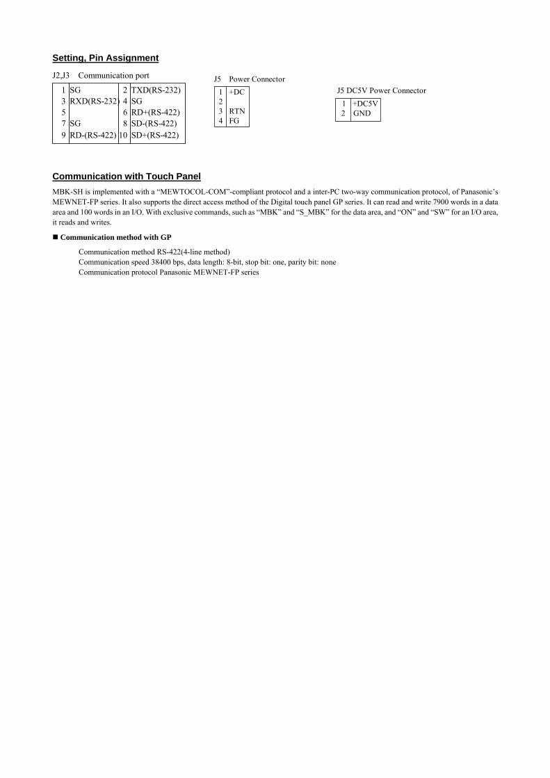
Setting, Pin Assignment J2,J3 Communication port
1 SG 2 TXD(RS-232) 3 RXD(RS-232) 4 SG 5 6 RD+(RS-422) 7 SG 8 SD-(RS-422) 9 RD-(RS-422) 10 SD+(RS-422)
1 +DC 2 3 RTN 4 FG
J5 Power Connector
1 +DC5V 2 GND
J5 DC5V Power Connector
Communication with Touch Panel MBK-SH is implemented with a “MEWTOCOL-COM”-compliant protocol and a inter-PC two-way communication protocol, of Panasonic’s MEWNET-FP series. It also supports the direct access method of the Digital touch panel GP series. It can read and write 7900 words in a data area and 100 words in an I/O. With exclusive commands, such as “MBK” and “S_MBK” for the data area, and “ON” and “SW” for an I/O area, it reads and writes.
Communication method with GP
Communication method RS-422(4-line method) Communication speed 38400 bps, data length: 8-bit, stop bit: one, parity bit: none Communication protocol Panasonic MEWNET-FP series

M
PC-SLINK S-LINK I/O Board
Specification S-LINK module SL-MC2 (made by Sanks): 2 pieces I/O 128 points / 1 module Number of supported MPCs 4 pieces (I/O 1024 points) Power supply DC 24V (for driving I/O) Consumed current DC 5V 200 mA./ board (supplied from the bus) Operating temperature 0~50°C
Hardware Construction
J2
J3
J1
DIP1
DIP2
LED7 1~2
SW1
ON
1 2
3 4
5 6
7 8
DIP1
DIP2
ON OFF
ON OFF
M1
M2
Switch for M1
Switch for M2
Setting for board address
Setting for number of IO ports When set to OFF position, the bit will read one. Setting for designating each bank as input or output. When set to OFF position, the bank is output.
No function
00
B1 B0
II
96-12764-95
II
32-630-31
11OOOO
S1 S0
00
11
OFF
00
B1 B0
II
96-12764-95
II
32-630-31
11OOOO
OFF
LED1~3
SW2
LED7 3~4
LED4~5
LED6~10
(1)
ON
1 2
3 4
5 6
7 8
Accessories: (1) Housing (5557-08R) Molex *2 J1, 2
Mounted connector
J1, 2 5569-08A1 Molex J3 5569-04A1 Molex
M1, 2 S-LINK host module J1 M1-side S-LINK port J2 M2-side S-LINK port J3 I/O-driving power LED1~4 (Red) M1-side error display LED~9 (Red) M2-side error display LED5 (Green) M1-side in operation (blinking) LED10 (Green) M2-side in operation (blinking) DIP1 Setting board address and M1-side I/O DIP2 Setting M2-side I/O SW1, 2 Reset button

Board Address As the board address, assigned are S0 and S1 of DIP1. The I/O numbers assigned by the board address change according to the following table. Also, MPC-SLINK is loaded with two S-LINK modules. J1 side is smaller number side and J2 side is larger number side, where each controls 28 points, totaling 256 points. If the J2-side module is not loaded, the corresponding I/O area becomes without numbers.
DIP-SW 2000~ 2256~ 2512~ 2768~ 2255 2511 2767 3023
DIP1~7 S0 OFF ON OFF ON
DIP1~8 S1 OFF OFF ON ON
I/O number
(ON=0, OFF=1) * All OFF when shipped out of factory
Setting, Pin Assignment
(1) J1, J2 Communication Port1 GND2 GND3 GND4 GND5 +246 D7 +248 LOOP
(2) J3 Power Connector1 GND2 GND3 +244 +24
J1J2J3
4 32 1
8 7 6 54 3 2 1
Substrate
8 7 6 54 3 2 1
Connection Example Please refer to Sanks S-LINK Instruction Manual for wiring. Next, shown are pin assignment and basic connection of each connector.
+24 GND D GND +24 GND LOOP GND
5 1 6 2 7 3 8 4
BrownBlue WhiteBlack +24 GND
·Although it is possible to connect power from the J3 side, current would be concentrated. For this reason, please use it only when the total is 3 A or less.
·In the case of the LOOP connection, the 7 and 8 side of J1 and J2 are used. ·J1 and J2 are independent S-LINKs. ·Each of +24 and GND of J1, J2, and J3 is internally shorted.
Concerning Display and Switches Setting the Dip Switches
DIP1~4
DIP-SW I/O No. I (ONside)
O (OFFside)
1 0~31
Input Output2 32~633 64~954 96~127
Attention) When setting by a program,please set all Low.
Rem) Input/output of the S-LINK system is set. ·I/O number can be switched between input and output by the unit of 32 points. ·Setting is taken in only once when the CPU-side power is turned on or releasing RESET. ·Please be careful because it is invalid even if changed during operation.

Rem) Number of I/Os of the S-LINK system is set. DIP5~6No. of I/Os B1(6) B0(5)
32 ON ON64 ON OFF96 OFF ON128 OFF OFF
(ON=0,OFF=1)
·System address length can be changed by the unit of 32 points. ·Setting is taken in only once when the CPU-side power is turned on or releasing RESET. ·Please be careful because it is invalid even if changed during operation.
Display
LED5,10(green) blinks during the S-LINK operation. Red LED signifies the error display. (Refer to Statis Acquisition.) For 7 seg display, refer to “S-LINK Instruction Manual”.
Status Acquisition Use IN function to acquire the status of S-LINK module.
Form IN(1999) /* Acquire the status of SLNK#1 IN(1998) /* Acquire the status of SLNK#2 IN(1997) /* Acquire the status of SLNK#3 IN(1996) /* Acquire the status of SLNK#4
Description T he return value is displayed in hexadecimal form.
&H n 0A 0B
n: hardware status 2: bug of J1 side, 1: bug of J2 side module 3: both side bug, with infufficient power supply 0A: bug of J1 side module 0B: bug of J2 side module
C
ontents of 0A and 0B, and the Corresponding LED
bit features J1 side module Red LED
J2 side module Red LED
7~4 (system) 3 ERR4(1: Disconnection or error input/output unit) LED4 LED9
2 ERR3(1: Abnormal level of power voltage of D-G) LED3 LED8
1 ERR2(1: No setting of I/O point numbers) LED2 LED7
0 ERR1(1: Short-circuit between D and G) LED1 LED6 ・ERR1 and ERR3 occurs on S-LINK side at the time of disconnection of the power supply. They are cancelled after the restoraton of power. ・ERR4 stays until it is manually cancelled. To cancel, turn off the power supply or input RESET after fixing the disconnection of the S-LINK
system. #PRX IN(1999) 00030505 /* 3= power supply is out. 05=ERR1,ERR3
Supprt: MPC-684 REV-3.82n or later

Rack 68K (3)
Please insert the board by paying attention to the top and bottom of the bus board and matching the pin numbers on the card edge and the silk-printed numbers of the bus board.
130 13.420.6
164
164
166
2
2×4-Ø3.1
116.424.5
80 99 112
10049.5
44.5
194
Cut-out (the other side)
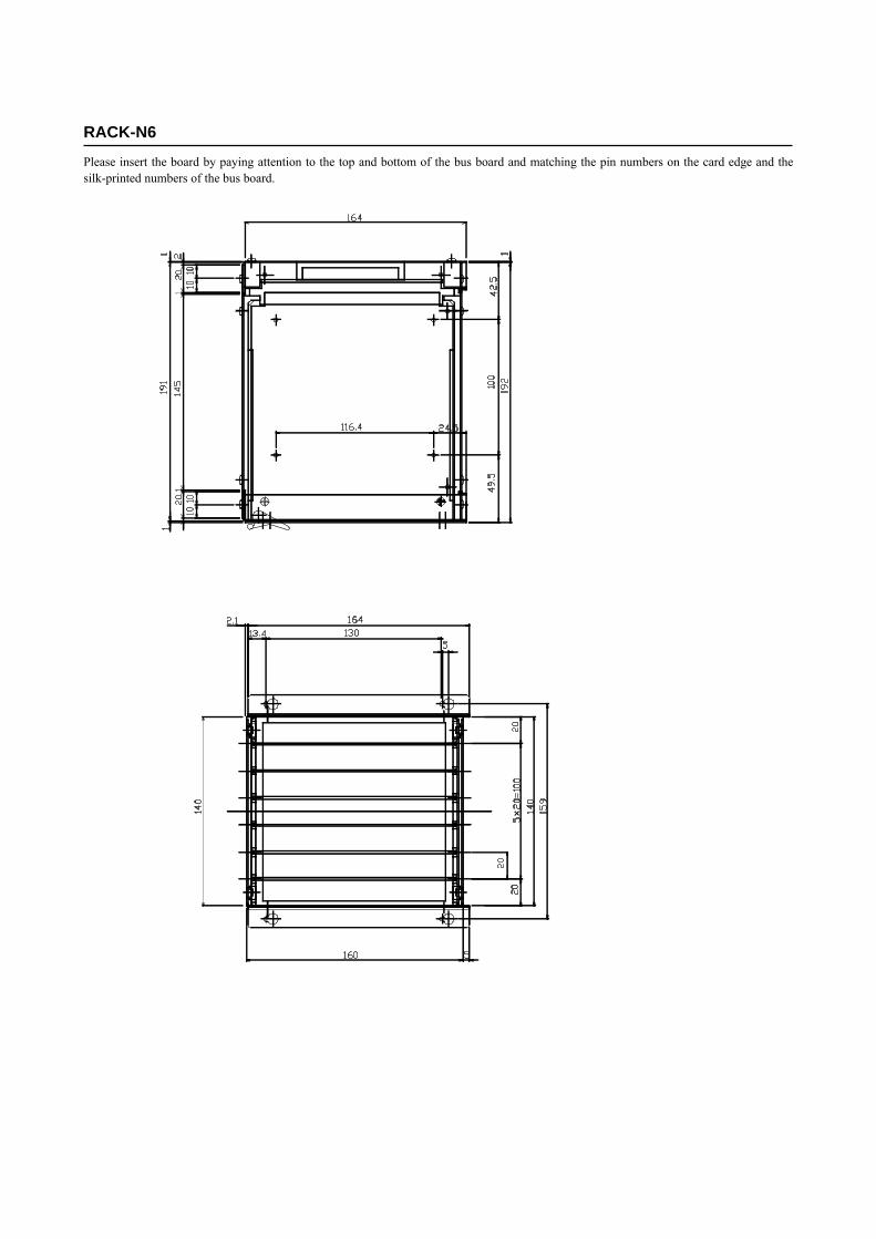
RACK-N6
Please insert the board by paying attention to the top and bottom of the bus board and matching the pin numbers on the card edge and the silk-printed numbers of the bus board.

RACK-N13
Please insert the board by paying attention to the top and bottom of the bus board and matching the pin numbers on the card edge and the silk-printed numbers of the bus board.

Cable Diagram
PC side 1 C D 2 RXD 3 TXD 4 DTR 5 S G 6 DSR 7 RTS 8 CTS 9 CI
MPC side S G 1 TX0 2 RX0 3 S G 4 MAN 5 P 5 6
3000mm
Hirose HDEB-9S equivalent
Hirose HIF-3BA-10D-2.54C equivalent
This is a manufacturer-original cable to connect an MPC and a PC. Although the basic cable is for DOS/V, a 25-pin conversion connector is attached, which allows use with a PC98 as it is.
Board External Form Illustration
169.4+-0.4
10.0+-0.2
2-Ø40+-0.15 Card pla attaching hole
No part loading prohibited here.
Front-side terminal B50Back-side terminal A50
Front-side terminal B1Back-side terminal A1
7.62 2-C1.0 2-R1.0
1.6-+0.2
5.0
8 5
.08
2.3
2+-0
.05
9.1
+-0.
2 1
48.7
+-0.
4
129
.1+-
0.1
2.5
4×49
=124
.46+
-0.1
5