
CHAPTER – 6 IMPLEMENTATION OF 128 POINT FFT...
22
66 CHAPTER – 6 IMPLEMENTATION OF 128 POINT FFT PROCESSOR USING R42MDC ARCHITECTURE Table of Contents Page No. 6.0 IMPLEMENTATION OF 128 POINT FFT PROCESSOR USING R42MDC ARCHITECTURE 67 6.1 Introduction 67 6.2 Comparison of Pipeline Architectures 68 6.3 Complex Addition and Multiplication 72 6.4 Cached-Memory Architecture (CMA) 74 6.5 The Mixed Radix 4/2 Computation Element 76 6.6 The FFT processor using R42MDC 81 6.7 Results and Discussion 84 6.8 Summary 87
Transcript of CHAPTER – 6 IMPLEMENTATION OF 128 POINT FFT...
66
CHAPTER – 6
IMPLEMENTATION OF 128 POINT FFT PROCESSOR USING R42MDC ARCHITECTURE
Table of Contents
Page No.
6.0 IMPLEMENTATION OF 128 POINT FFT PROCESSOR
USING R42MDC ARCHITECTURE 67
6.1 Introduction 67
6.2 Comparison of Pipeline Architectures 68
6.3 Complex Addition and Multiplication 72
6.4 Cached-Memory Architecture (CMA) 74
6.5 The Mixed Radix 4/2 Computation Element 76
6.6 The FFT processor using R42MDC 81
6.7 Results and Discussion 84
6.8 Summary 87
67
CHAPTER – 6
IMPLEMENTATION OF 128 POINT FFT PROCESSOR USING R42MDC ARCHITECTURE
6.1 INTRODUCTION
The Fast Fourier transformation (FFT) is periodically employed in the algorithms
of signal processing for the applications of Orthogonal Frequency Division
multiplexing (OFDM). The architectures of FFT adopted for OFDM can be
categorized into three types- pipeline architecture, memory architecture and parallel
architecture [8]. The pipeline and parallel architectures utilize more number of
butterfly elements to obtain better performance but they occupy larger area when
compared to the third architecture. The memory architecture employs a single
butterfly element possessing the advantage of less area. This chapter concentrates on
the memory architecture for small area and simplicity of hardware to build a
compatible OFDM system. The suggested 128-point FFT processor is based on
Cached-memory architecture (CMA) and Mixed Radix 4/2 multiple delay
commutator (R42MDC) algorithm. The implementation of FFT processor has been
adopted using the above methodology to achieve consumption of power and size of
chip. The size of chip is realized as 2.8 x 2.8 mm2 with standard 0.35 μm CMOS
technology. The consumption of power with this architecture is 72 mW at a frequency
range of 127-133 MHz which is less than 50 % of traditional 128-Point FFT design
with standard 0.18 µm CMOS technology. The various types of pipeline architectures
such as MDC, SDF, and SDC are compared using the above technique against the
implementation of a 128-point FFT processor with respect to size of memory,
consumption of area and power.
68
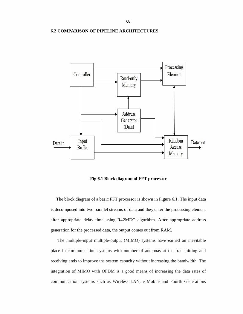
6.2 COMPARISON OF PIPELINE ARCHITECTURES
Fig 6.1 Block diagram of FFT processor
The block diagram of a basic FFT processor is shown in Figure 6.1. The input data
is decomposed into two parallel streams of data and they enter the processing element
after appropriate delay time using R42MDC algorithm. After appropriate address
generation for the processed data, the output comes out from RAM.
The multiple-input multiple-output (MIMO) systems have earned an inevitable
place in communication systems with number of antennas at the transmitting and
receiving ends to improve the system capacity without increasing the bandwidth. The
integration of MIMO with OFDM is a good means of increasing the data rates of
communication systems such as Wireless LAN, e Mobile and Fourth Generations
69
(4G) in the near future [6]. Since MIMO-OFDM system transmits multiple streams of
data, it needs various processors with increasing complexity of hardware when
compared to single-input single-output OFDM (SISO-OFDM) systems. Since the FFT
processor is a complex module in OFDM, it is highly inevitable to design the
processor in an efficient way.
The architectures of pipelined FFT processor can be divided into ‘3’ types –
Single Delay Feedback (SDF), Multiple Delay Commutator (MDC) and Single delay
commutator (SDC). Among these architectures, the SDF architecture is appropriate to
manipulate FFT for OFDM systems with single channel because it needs only one
input or output path and less resources of hardware [7]. However, in MIMO-OFDM
systems, the SDF style is not the correct approach to manipulate the FFT. Because of
its single input or output path and lower performance, various FFT processors based
on SDF will be required to adopt a MIMO-OFDM system. Contrary to SDF, the MDC
style has more number of input or output paths. For example a 4-channel R42MDC
FFT processor can access four channels of data at a time. It needs an additional
commutator circuit for transforming the four input data streams in a simultaneous
manner. This additional commutator can be included by simple delay elements and a
multiplexer. But the MDC architecture is not a good choice from the idea of hardware
complexity which can be decreased further by utilizing a mixed-radix algorithm. The
FFT based on mixed radix algorithm and single delay commutator (SDF) style is
already explained in Chapter 5. However the FFT processors based on multiple delay
commutator (MDC) and single delay commutator (SDC) styles are shown in Figure
6.2 and Figure 6.3 respectively. The R42MDC and R42SDC architectures shown in
Figure 6.2 and Figure 6.3 respectively are disintegrated to log 4/2 N stages. In these
architectures, every stage comprises a commutator, a butterfly and a complex

70
multiplier. The respective control signals are produced by the logic functions. The
butterfly element does the summation operation in which the multiplication is
substuited by add or subtract and swapping of real or imaginary parts. Comparatively
SDF style outperforms the SDC style in terms of higher performance due to its
simplicity and compatibility with pipelining [4]. Keeping all the above facts in mind,
the MDC architecture along with mixed radix algorithm is chosen for the proposed
128 point FFT processor.
Fig. 6.2 FFT processor based on Multiple Delay Commutator (MDC)

71
Fig. 6.3 FFT processor based on Single Delay Commutator (SDC)
72
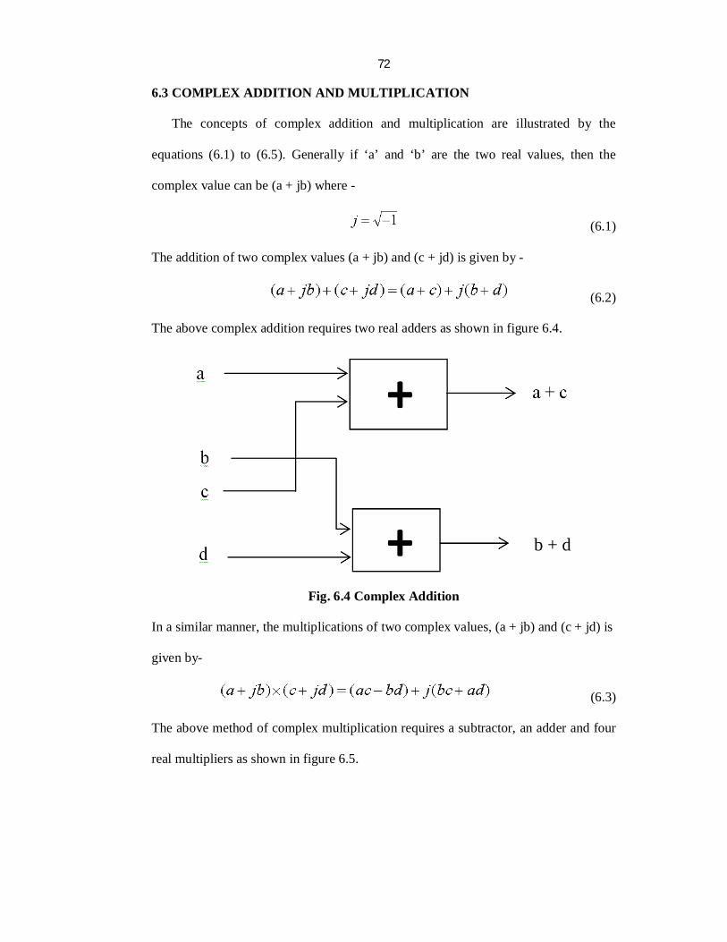
6.3 COMPLEX ADDITION AND MULTIPLICATION
The concepts of complex addition and multiplication are illustrated by the
equations (6.1) to (6.5). Generally if ‘a’ and ‘b’ are the two real values, then the
complex value can be (a + jb) where -
(6.1)
The addition of two complex values (a + jb) and (c + jd) is given by -
(6.2)
The above complex addition requires two real adders as shown in figure 6.4.
Fig. 6.4 Complex Addition
In a similar manner, the multiplications of two complex values, (a + jb) and (c + jd) is
given by-
(6.3)
The above method of complex multiplication requires a subtractor, an adder and four
real multipliers as shown in figure 6.5.
b + d

73
Fig. 6.5 Complex Multiplication-1
The same complex multiplication can be done in the other way. The two complex
values (a + jb) and (c + jd) can be multiplied and reduced by the equations (6.4) and
(6.5) given below-
Real part = (ac – bd) – (ad + ad)
= a (c - d) + d (a - b) (6.4)
Imaginary part = ad + bc – bd + bd
= d (a - b) + b (c + d) (6.5)
This method of complex multiplication requires three real multipliers, two subtractors
and three adders as shown in Figure 6.6.
Fig. 6.6 Complex Multiplication-2
74
6.4 CACHED-MEMORY ARCHITECTURE (CMA)
The cached memory architecture (CMA) does a computation of higher radix with
good performance and less power. Figure 6.7 shows the block diagram of system
using Cache Memory Architecture. It includes a cache housing a set of registers
between the main memory and the computation element and it is almost similar to a
memory architecture having a single memory. This set of registers is used to hide the
memory access cycle behind the cycle of computation as shown in Figure 6.8. This
combination of cache-processor in a tightly-coupled manner improves the bandwidth
to the main memory during execution and the processor need not access the main
memory frequently. The improvements in VLSI technology have improved the
efficiency of FFT processors and also emphasize the need for higher-radix
computation. The expressions for memory access cycle and execution cycle are given
by equations (6.6) and (6.7) with the computation element having a single mixed
radix 4/2 execution unit.
Memory Access Cycle = r * 2 (6.6)
Execution Cycle = r * [log r N] / 2 (6.7)
Where
r - Radix number
N - Length of FFT
Fig. 6.7 Block diagram of the System using CMA

75
Fig. 6.8 Operation sequence for each register in CMA
Equations (6.6) and (6.7) show that ratio of the execution cycle to the memory
access cycle becomes smaller with increase in radix number. This indicates that if the
radix number increases, the execution time becomes greater than the memory access
time which creates imbalance as shown in Figure 6.8. Hence multiple units of
computation with multiple data path are needed to solve the imbalance. Hence a
computation element having multiple data path has been developed without any
bottleneck created by various factors such as bus, crossbar or network structure.
The suggested cached-memory architecture is shown in Figure 6.9. The cached-
memory architecture is highly preferable because a hierarchical memory system will
be needed to harvest the advantages of the FFT algorithm. The system performance
can be enhanced by including a second set of cache. By this method of arrangement,
the processor uses one set of cache for operation while the main memory uses other
set of cache for flushing and loading the data simultaneously. If the load time and

76
flushing time of the algorithm is less than the data processing time inside the cache,
then the processor becomes free and not requires the cache between groups. Hence a
second set of cache enhances the performance of the processor at the cost of little
additional complexity.
Fig 6.9 Block Diagram of Cached-Memory Architecture
6.5 THE MIXED RADIX 4/2 COMPUTATION ELEMENT
In the Mixed Radix-4/2 FFT algorithm, transformation of a 8-word is performed
by a 4 x 3 butterfly operations as shown in Figure 6.10 (a). The butterfly unit is larger
which includes an adder, subtractor and a complex multiplier. Hence it becomes
inevitable to reemploy computational resources to reduce the area of the chip. To
obtain this, the Resource-saving Mixed Radix 4/2 computation element (RM-R4-2CE)
has been developed.
The data transits in groups of 8-words through the transform of 128-word since
each column of the matrix includes four independent butterfly elements. This idea of
symmetry decomposes the computation of 8-word into three passes as shown in

77
Figure 6.10 (b). The RM-R4-2CE unit includes execution units of Mixed Radix 4/2
butterfly and it processes each pass of the computation. Hence all sort of
communication can be regulated using RM-R4-2CE and saved in the register near to
subsequent butterfly element by modifying the address of the data inside the cache in
a regular manner. In this way, RM-R4-2CE unit can decrement the area of processor
to 33% and the interconnection area to 50% without any penalties of delay.
Fig. 6.10 Dataflow diagram of the 8-word group
(a) Decomposition of Radix-2 (b) Computation element
78
Figure 6.11 shows the block diagram of computation element (RM-R4-2CE) with
a set of registers. In traditional FFT the pipeline style is deeply adopted in a regular
manner. But every entry of data is processed inside the processor and the cache in a
cyclic manner in RM-R4-2CE. Therefore the complex controllers and additional
pipeline registers are not all required. Thus this architecture eliminates memory
bottleneck and processor stalls due to data dependency. The RM-R4-2CE includes
routing switches for routing the output signals to the respective registers for further
processing. In figure 6.11, if the select signal is ‘0’, the configuration of first and third
pass will be adopted on RM-R4-2CE, and if the select signal is ‘1’, then the
configuration of second pass is adopted.

79
Fig. 6.11 Block diagram of RM-R4-2CE with a set of registers
The cycle of execution reaches non- critical due to the effects of multiple data
path. Hence the multiplier inside the butterfly execution unit is kept as small as
possible. Table 6.1 and 6.2 shows the computation of count of gates for both the adder
and multiplier. From the tabulation of results, the array multiplier and the ripple carry
adder have been selected for the architecture. They can decrement the complex
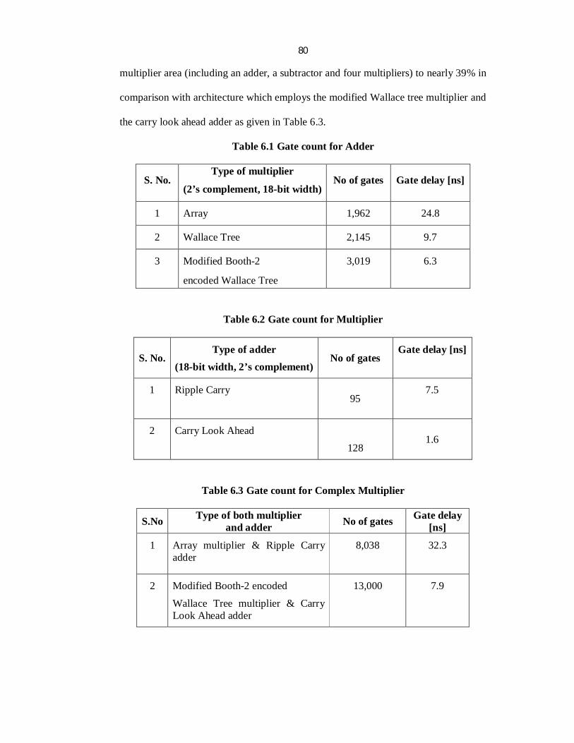
80
multiplier area (including an adder, a subtractor and four multipliers) to nearly 39% in
comparison with architecture which employs the modified Wallace tree multiplier and
the carry look ahead adder as given in Table 6.3.
Table 6.1 Gate count for Adder
S. No. Type of multiplier
(2’s complement, 18-bit width) No of gates Gate delay [ns]
1 Array 1,962 24.8
2 Wallace Tree 2,145 9.7
3 Modified Booth-2
encoded Wallace Tree
3,019 6.3
Table 6.2 Gate count for Multiplier
S. No. Type of adder
(18-bit width, 2’s complement) No of gates
Gate delay [ns]
1 Ripple Carry
95
7.5
2 Carry Look Ahead
128
1.6
Table 6.3 Gate count for Complex Multiplier
S.No Type of both multiplier and adder No of gates Gate delay
[ns]
1 Array multiplier & Ripple Carry adder
8,038
32.3
2 Modified Booth-2 encoded
Wallace Tree multiplier & Carry Look Ahead adder
13,000
7.9

81
The data from the main memory has been read into the register, processed for
manipulations and written to the main memory in a serial manner. The data is routed
for three passes around the RM-R4-2CE and the register during the period of
execution. Then the processing of 3-stage pass is completed within the period
equivalent to that of read time of an 8-word data. It is inferred clearly that the RM-
R4-2CE unit transforms the data without any delay even though the number of
butterfly elements or the interconnect resources are reduced appropriately. Hence the
suggested RM-R4-2CE is correctly suitable for the manipulations of FFT based on
Cache memory architecture.
The processor will be subjected to wait for data in CMA without using the double
buffer structure on the other hand. This is highly inevitable for small area and speed
efficient FFT processors of two dimensions. The dual-port SRAM can be employed in
pipeline FFT processors in order to increase the width of data path. Since dual-port
SRAM consumes more area comparatively, it is highly difficult to implement the
double buffer. But CMA along with RM-R4-2CE can obtain an efficiency of 100%
with the configuration of single-port SRAM. This indicates that the integration of
RM-R4-2CE, CMA and the double buffer structure is highly suitable for the
suggested FFT processor.
6.6 THE FFT PROCESSOR USING R42MDC
There are two categories of mixed-radix algorithms of FFT. With relevant to the
first method, the Radix-q algorithm is applied to a series of ‘N’ spaced points and the
steps of Radix-2 are implemented either at the start or end of the transform using
MDC architecture. This design technique integrates the important features of less
memory, complete utilization of multiplier and simple control logic by employing
mixed radix 4/2 algorithm with MDC style. Both the Mixed Radix-4/2 algorithm and
82
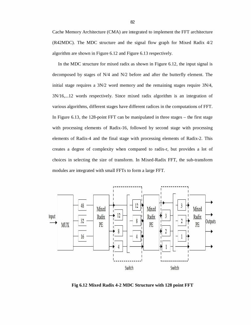
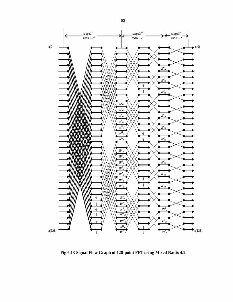
Cache Memory Architecture (CMA) are integrated to implement the FFT architecture
(R42MDC). The MDC structure and the signal flow graph for Mixed Radix 4/2
algorithm are shown in Figure 6.12 and Figure 6.13 respectively.
In the MDC structure for mixed radix as shown in Figure 6.12, the input signal is
decomposed by stages of N/4 and N/2 before and after the butterfly element. The
initial stage requires a 3N/2 word memory and the remaining stages require 3N/4,
3N/16,...12 words respectively. Since mixed radix algorithm is an integration of
various algorithms, different stages have different radices in the computations of FFT.
In Figure 6.13, the 128-point FFT can be manipulated in three stages – the first stage
with processing elements of Radix-16, followed by second stage with processing
elements of Radix-4 and the final stage with processing elements of Radix-2. This
creates a degree of complexity when compared to radix-r, but provides a lot of
choices in selecting the size of transform. In Mixed-Radix FFT, the sub-transform
modules are integrated with small FFTs to form a large FFT.
Fig 6.12 Mixed Radix 4-2 MDC Structure with 128 point FFT
83
Fig 6.13 Signal Flow Graph of 128-point FFT using Mixed Radix 4/2

84
6.7 RESULTS AND DISCUSSION
The Modelsim and VHDL language are used for simulation and verification at the
algorithmic level due to their high speed of execution. A number of simulations at
different levels of abstraction are performed. Then the design architecture is
synthesized by using Xilinx’s Virtex-II Pro FPGA. Table 6.4 shows the complete
details of consumption of area and power for the designed 128 point FFT processor in
comparison with the traditional FFT design. Further various types of pipeline
architectures such as Single Delay Feedback (SDF), Single Delay Commutator (SDC)
and Multiple Delay Commutator (MDC) have been compared with respect to size of
memory, consumption of power and area as shown in Table 6.5. Among these
architectures, the MDC seems to be better in terms of area, memory and power.
Figure 6.14 shows the corresponding graph for comparison of these pipeline
architectures.
Table 6.4 Consumption of Area and Power of 128-point FFT using MDC
128 –Point FFT
Parameter/Type Conventional Design
Proposed Design
Frequency (MHz)
Memory size (words) 128 91 127-133 Area (gate count) 51,000 41990.5 127-133
Power Consumption (mW)
137 72 127-133
Table 6.5 Comparison of Pipeline Architectures with 128 point FFT
Type of Architectures
Memory size (Words) (Increase/Decrease)% Power (mW) Area (mm2) Frequency
(MHz) MDC 91 (26.7) 72 7.84 127-133
SDF 267 (60.5) 141.9 22.50 154
SDC 245 (50) 90.6 21.25 133

85
Table 6.6 Other features of the proposed 128-point FFT processor
S.No Parameters Proposed FFT Spiffee NTT LSI Lab 1 Technology
0.35 μm 0.7 μm
0.8 μm
2 Data path width
36 x 8-bit fixed point
20-bit fixed point
24-bit Floating
3 Area 7.84 mm2 49 mm2 134 mm2 4 Clock Freq. 127-133 MHz 173 MHz 40 MHz 5 128-point FFT 23.2 μs 15 μs 54 μs
Fig 6.14 Comparison of Pipeline Architectures
This processor has been implemented with standard 0.35 μm technology with an
area consumption of only 7.84 mm2. It comprises 3, 60,000 transistors for SRAM and
1, 92,000 transistors for logic in terms of ‘3’ blocks. Out of these blocks, two blocks
are allocated for data and the third block saves the twiddle factor coefficients. Table
6.6 shows the other important features of the implemented FFT processor in
comparison with the previous processors. This table shows that the suggested FFT

86
processor is better in terms of width of data path, speed of calculation and silicon area
in spite of various differences in implementation. Moreover instead of ROM, the
SRAM coefficients are used for storing the twiddle factors. Figure 6.15 shows the
simulation results for power. Figure 6.16 shows the chip size of the 128-point FFT
processor based on R42MDC and CMA.
Fig 6.15 Simulation Results for Power - 128 point FFT Processor

87
Fig 6.16 Chip Size of 128-point FFT Processor
6.8 SUMMARY
In this chapter, the 128 point FFT processor is implemented using cache memory
architecture (CMA) and Mixed Radix 4/2 multiple delay commutator (R42MDC)
algorithm. This utilizes an optimum memory structure with improved performance,
developed with less dissipation of power, small consumption of area and low
operating frequencies. The various types of pipeline architectures such as MDC, SDF,
and SDC are compared and verified using the above technique. The consumption of
power with this architecture is 72 mW which is less than 50 % that of traditional 128-
Point FFT design at a frequency range of 127-133 MHz. This design architecture can
be employed for the applications specifically in OFDM and wideband communication
systems. The processor has been realized by employing Modelsim and VHDL for
generating simulation results and coding the design respectively.

![Low Power QDI Asynchronous FFT · 14 This Work Sync (Chip)* [1] [2] Tech 65 nm 65 nm 65 nm 0.35 µm Voltage 1.0 V 1.0V 0.3 V 1.1 V N-point 128 128 128 128 Data rate 10 MHz 10 MHz](https://static.fdocuments.us/doc/165x107/5f814800ade84214b13146d3/low-power-qdi-asynchronous-fft-14-this-work-sync-chip-1-2-tech-65-nm-65-nm.jpg)


![Study of WiMAX Based Communication Channel Effects on ...where the size of the FFT is changeable and may be equal to: 128, 512, 1024, and 2048 [13]. 2048 FFT was adopted through this](https://static.fdocuments.us/doc/165x107/60722ab09c1d577c547950bb/study-of-wimax-based-communication-channel-effects-on-where-the-size-of-the.jpg)