Chapter 5 Epitaxial Growth of Si1-yCy Alloys
123
119 Chapter 5 Epitaxial Growth of Si 1-y C y Alloys 5.1 Introduction Traditionally, the incorporation of substitutional carbon into silicon and silicon- germanium alloys during growth is of great interest for engineering the strain in silicon layers. Carbon incorporation in SiGe can be used to compensate the compressive strain in SiGe layers grown commensurately w.r.t. silicon. As little as 1% carbon can compensate for the compressive strain induced by 10% Ge in silicon. Achieving high substitutional carbon fraction (> 1% carbon) in Si 1-y C y alloys is important to achieve significant strain for electron mobility improvement by compressively straining the silicon channel. The growth of epitaxial strained silicon-carbon alloys on Si (100) substrates is used in the source-drain regions of MOSFETs to induce tensile stress in channel regions to enhance electron carrier mobility [5.1][5.2]. Carbon in silicon has also been shown to reduce the boron diffusion in silicon [5.3][5.4][5.5]. Only a small fraction of carbon (10 19 cm -3 ) [5.3] needs to be incorporated to suppress the diffusion of boron. This was effect was used for the growth of Si 1-x-y Ge x C y bases for hetero-bipolar junction transistors (HBTs). 5.2 Growth of Si:C Alloy Layers There are several challenging issues in the growth of Si 1-y C y alloys. First, unlike growth with Si 1-x Ge x where it is easy to achieve high Ge fractions, it is difficult to achieve high substitutional carbon percentages in silicon. This is due to a significantly larger lattice mismatch between silicon and diamond (35%) than the lattice mismatch
Transcript of Chapter 5 Epitaxial Growth of Si1-yCy Alloys

119
Chapter 5
Epitaxial Growth of Si1-yCy Alloys 5.1 Introduction
Traditionally, the incorporation of substitutional carbon into silicon and silicon-
germanium alloys during growth is of great interest for engineering the strain in silicon
layers. Carbon incorporation in SiGe can be used to compensate the compressive strain in
SiGe layers grown commensurately w.r.t. silicon. As little as 1% carbon can compensate
for the compressive strain induced by 10% Ge in silicon. Achieving high substitutional
carbon fraction (> 1% carbon) in Si1-yCy alloys is important to achieve significant strain
for electron mobility improvement by compressively straining the silicon channel. The
growth of epitaxial strained silicon-carbon alloys on Si (100) substrates is used in the
source-drain regions of MOSFETs to induce tensile stress in channel regions to enhance
electron carrier mobility [5.1][5.2]. Carbon in silicon has also been shown to reduce the
boron diffusion in silicon [5.3][5.4][5.5]. Only a small fraction of carbon (1019 cm-3) [5.3]
needs to be incorporated to suppress the diffusion of boron. This was effect was used for
the growth of Si1-x-yGexCy bases for hetero-bipolar junction transistors (HBTs).
5.2 Growth of Si:C Alloy Layers
There are several challenging issues in the growth of Si1-yCy alloys. First, unlike
growth with Si1-xGex where it is easy to achieve high Ge fractions, it is difficult to
achieve high substitutional carbon percentages in silicon. This is due to a significantly
larger lattice mismatch between silicon and diamond (35%) than the lattice mismatch

120
between Si and Ge (4.2%). Second, a stable phase, silicon carbide (SiC) exists between
silicon and diamond. Third, carbon also has a low solubility (3*1017/cm3) in silicon [5.6]
[5.7]. Substitutional carbon incorporated into silicon layers at a level above this value
will be supersaturated. Fourth, nonsubstitutional carbon is observed to create deep levels
in silicon [5.8]. Thus the carbon should be incorporated into a substitutional site and not
an interstitial site.
Due to these difficulties, non-equilibrium growth techniques such as MBE and
CVD are used to incorporate a high metastable substitutional carbon fraction
[5.9][5.10][5.11]. Such non-equilibrium growth causes the buried carbon to be
immobilized on the substitutional site [5.12][5.13].
Figure 5.1. Plot of substitutional carbon (measured by the shift in lattice constant by x-ray diffraction) vs. total carbon measured by SIMS [5.11]
From Figure 5.1, the difficulty in the growth of silicon with high carbon percentages is
clearly illustrated. From the “fully substitutional” line drawn in Figure 5.1, we observe

121
that at high temperatures, the carbon incorporates interstitially rather than
substitutionally. Lowering the temperature causes more carbon to incorporate into
substitutional sites. This illustrates the importance of metastable growth for the
incorporation of carbon in silicon, as the carbon atoms on the surface cannot be given
enough time to reach their favored (equilibrium) position of being an interstitial.
Furthermore, it has been demonstrated in reference [5.11] and in the work of other
authors [5.9][5.10] that by using a high growth rate at low temperature more carbon can
be incorporated into substitutional sites. As described earlier (Chapter 2) the combination
of high growth rate and low temperature are difficult to achieve in CVD epitaxy using
silane. The growth of Si1-yCy alloys using DCS as a silicon source (lower growth rate than
with silane due to its chlorinated chemistry) and methylsilane [5.11] also indicates that a
high growth rate is a necessity for high substitutional carbon incorporation. Therefore, to
incorporate high carbon fractions (>1% carbon in silicon) higher-order silanes are
potentially attractive to be used as the silicon source gas because high rates and low
temperatures should help for substitutional carbon incorporation. We examined the use of
NPS as a silicon source for achieving this goal.
5.3 Determining Substitutional Carbon Fraction in Silicon:
Dilute Carbon Alloys
Due to the difference in lattice constant, thin silicon carbon alloy epitaxial layers may be
grown pseudomorphic on silicon substrates. The Si:C alloy layer is tensilely strained in
the planar directions and compressively strained in the vertical (growth) direction, as
shown in Figure 5.2 below.

122
Figure 5.2. Schematic diagram illustrating the silicon substrate lattice and the growth of the pseudomorphic Si:C alloy layers on silicon substrate.
The vertical (004) lattice spacing of the compressively strained layers, a⊥ can be
determined via x-ray diffraction (XRD) based on the shift from the substrate peak. From
a⊥, the carbon percentage can be extrapolated using Poisson’s ratio and Vegard’s law
[5.14][5.15]:
This is rewritten in the equation below for simplicity:
Eq. 5.1 [ ]Sirelaxed
CSirelaxed
CSiCSi aaxCxCaa
xxxxxx−+=
−−−
⊥
111 )()(2
12
11
⎟⎟
⎠
⎞
⎜⎜
⎝
⎛ −
−+
=⎟⎟
⎠
⎞
⎜⎜
⎝
⎛ −−−
⊥
Si
Sirelaxed
CSi
Si
SiCSi
a
aa
a
aayyyy 11
11
υυ

123
where C11(x) and C12(x) are the elastic constants of Si1-xCx which are linearly
extrapolated from Si and C, a Si1-xCx relaxed is the unstrained bulk lattice constant of Si1-xCx,
a Si1-xCx┴ is the strained lattice constant of Si1-xCx , and aSi is the bulk unstrained lattice
constant of silicon (5.431 Ångstroms). The percentage of substitutional carbon varies
depending on what model is used for the relaxed lattice constant of Si1-xCx versus carbon
fraction. Vegard’s law could be applied between silicon and diamond or silicon and
silicon-carbide. An alternate method is proposed by Kelires [5.16] and is generally
accepted as the most accurate method in determining the substitutional carbon
percentage. However, in this thesis, we use Vegard’s law applied between silicon and
silicon-carbide.
5.4 Si:C Alloy Epitaxial Layers Grown with NPS and
Methylsilane
5.4.1 Growth of Si:C Epitaxial Layers Using NPS and Methylsilane
As described earlier, low temperatures and a high growth rate are generally
required for Si:C alloy growth with high substitutional carbon fractions. Si:C alloys were
grown with NPS as the silicon source and methylsilane (SiCH6) as the carbon source. The
growth pressure was 6 torr and the growth temperature was 575 oC. The thickness of the
Si:C epitaxial layers are ~100 nm. Figure 5.3, shows XRD scans done in Princeton, and
in Table 5.1 below are the corresponding gas flows of hydrogen, NPS and methylsilane
gas flows. The methylsilane source is diluted 1% in hydrogen. The methylsilane flow
given in the table is the actual methylsilane flow.

124
Figure 5.3. XRD rocking curves of various Si:C alloys grown at 575 oC and 6 torr pressure. The hydrogen, NPS and methylsilane flows are given in the table below. The growth thickness of the epitaxial layers is roughly 100 nm.
The two copper kα peaks are not fully resolved out in our experimental setup. We
determine the Si:C alloy strained lattice constant from the spacing between the two left
peaks. As observed from figure 5.3 above, as the carbon percentage is increased the
intensity of the peak is decreasing. At high carbon percentage (C > 2%) the two peaks are
difficult to distinguish. This could be due to relaxation of the silicon-carbon layers or a
reduction in the layer quality. Assuming the critical thicknesses for commensurately
strained Si1-xGex and tensilely strained Si1-yCy are similar for the same strain and
assuming that 1% carbon compensates for roughly 10% Ge [5.17], the metastable critical
thickness for Si0.985C0.015 layers is roughly 60 nm [5.18]. The results are summarized in
the Table 5.1 below.

125
Table 5.1. Summary growth conditions and substitutional carbon fraction of Si:C alloys grown with NPS and methylsilane as the silicon and carbon sources respectively at a chamber pressure of 6 torr and a temperature of 575 oC. Sample # Carbon
(XRD) %
H2 (sccm)
NPS Bubbler
Flow (sccm)
SiCH6 (sccm)
H2 (partial pressure)
NPS estimated (partial
pressure)
SiCH6 actual
(partial pressure)
Growth Rate
(nm/min)
1 1.1 600 50 1 5974 mtorr 17 mtorr 9 mtorr 10 2 1.3 150 50 1 5916 mtorr 54 mtorr 30 mtorr 24 3 1.8 150 30 1 5930 mtorr 36 mtorr 34 mtorr 18 4 2.35 150 20 1 5939 mtorr 25 mtorr 36 mtorr 13 5 2.6 150 15 1 5943 mtorr 20 mtorr 37 mtorr ?
In the table above we compare the substitutional (XRD) carbon levels in Si:C
alloys of five samples based on the H2, NPS (bubbler flow) and SiCH6 gas flows. From
the gas flows we also tabulated the actual partial pressures of H2, NPS and SiCH6. The
actual NPS flow was estimated to be 3.6% of the NPS bubbler flow (Section 2.2). As
observed from Table 5.1, the growth rate can be increases by increasing the NPS flow at
fixed pressure and constant hydrogen carrier flow. This requires a commensurate increase
in methylsilane flow to keep a high carbon concentration in the grown layer. Because
increasing the hydrogen into the NPS bubbler above 50 sccm caused temporary clogging
of our mass flow controller and increasing the methylsilane flow was limited by the
methylsilane flow controller to 1 sccm (100 sccm of 1% methylsilane in hydrogen), we
decreased our hydrogen flow while holding the hydrogen into the NPS bubbler at 50
sccm and held the methylsilane flow constant, as illustrated from the change in sample 1
to sample 2 in the table above. At fixed methylsilane/NPS flow ratio, we are increasing
both the partial pressure of NPS and methylsilane, hence growth rate, leading to an
increased carbon fraction. Once we were no longer able to decrease the hydrogen flow,
we instead reduced the NPS flow to increase carbon levels as shown in Table 5.1
(samples 3 to 5). This increases the methylsilane to NPS ratio leading to more carbon
being incorporated despite a reduction in the growth rate. Ideally, we would like to
126
increase both NPS with methylsilane while decreasing the hydrogen flow however due to
limitations in our experimental apparatus we were unable to do so.
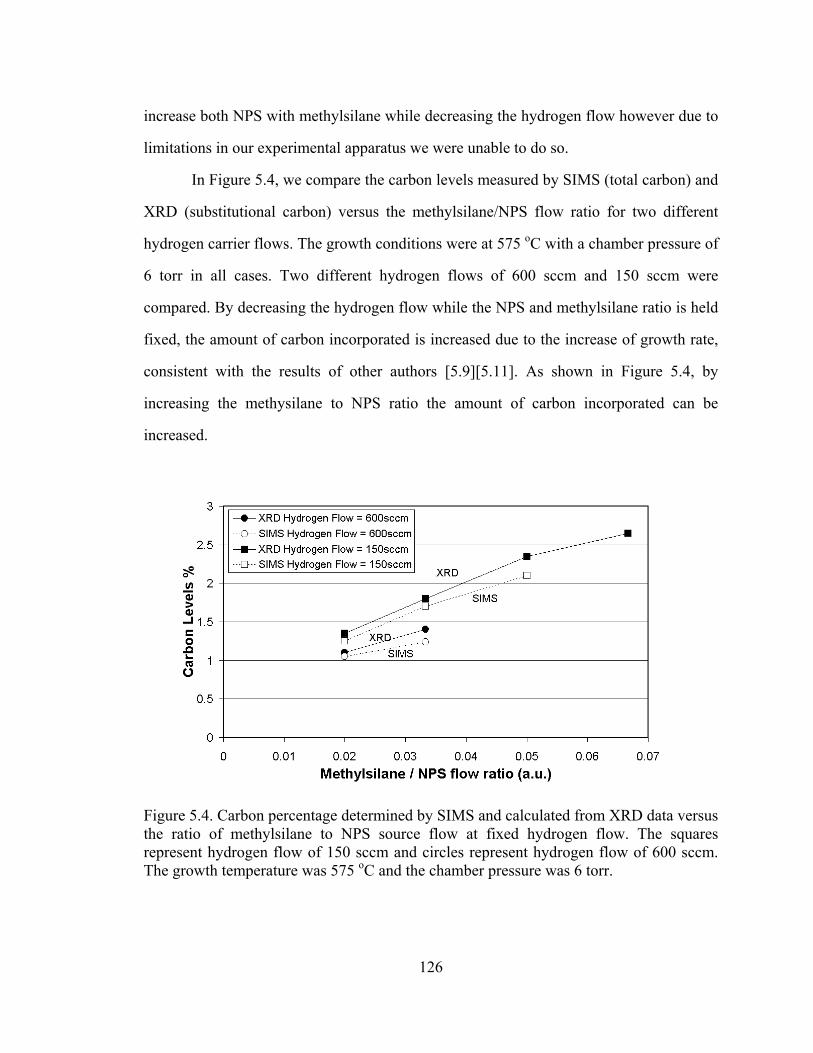
In Figure 5.4, we compare the carbon levels measured by SIMS (total carbon) and
XRD (substitutional carbon) versus the methylsilane/NPS flow ratio for two different
hydrogen carrier flows. The growth conditions were at 575 oC with a chamber pressure of
6 torr in all cases. Two different hydrogen flows of 600 sccm and 150 sccm were
compared. By decreasing the hydrogen flow while the NPS and methylsilane ratio is held
fixed, the amount of carbon incorporated is increased due to the increase of growth rate,
consistent with the results of other authors [5.9][5.11]. As shown in Figure 5.4, by
increasing the methysilane to NPS ratio the amount of carbon incorporated can be
increased.
Figure 5.4. Carbon percentage determined by SIMS and calculated from XRD data versus the ratio of methylsilane to NPS source flow at fixed hydrogen flow. The squares represent hydrogen flow of 150 sccm and circles represent hydrogen flow of 600 sccm. The growth temperature was 575 oC and the chamber pressure was 6 torr.

127
The substitutional carbon percentage calculated from the XRD was then
compared with the total carbon percentage determined from SIMS to determine if the Si1-
yCy alloys grown are fully substitutional. In Figure 5.5 below we compare substitutional
carbon (XRD) vs. total carbon (SIMS) for growth conditions at 575 oC and 6Torr, with
varying NPS, methylsilane and hydrogen flows. Relative error bars of 5% and 15% were
used for the XRD and SIMS measurements respectively.
Figure 5.5. Comparison of substitutional carbon percentage measured from XRD vs. total carbon percentage determined by SIMS. Relative error bars of 5% and 15% were used for the XRD and SIMS measurements respectively. The dotted line represents fully substitutional carbon.
The dotted line in the figure is used to depict fully substitutional carbon levels. If
the value calculated from XRD is equivalent to the carbon measured by SIMS then the
carbon incorporated is fully substitutional. If the carbon measured from SIMS is greater
than the carbon level determined from XRD then the carbon incorporated is partially
interstitial or the grown layer is relaxed, causing a reduction in the value calculated from

128
XRD. It can be inferred that fully substitutional carbon percentages up to 2.1% has been
achieved within the error bars of XRD and SIMS measurements.
To determine the quality of our Si1-xCx epitaxy layers, high resolution X-ray
diffraction (HR-XRD), (courtesy of Applied Materials) was performed on the as-grown
silicon-carbon alloy layer of 1.8% using the same conditions depicted in Table 5.1 above
and shown in Figure 5.3 above. The X-ray rocking curve of an ideal Si:C alloy layer of
1.8% carbon and 100 nm thickness was simulated. The HR-XRD and computer
simulation result is plotted in Figure 5.6 below:
Figure 5.6. High-Resolution X-Ray Diffraction (HR-XRD) of a 130nm Si1-yCy layer on Si showing a substitutional carbon level of 1.8% with lattice constant of 5.375Å. The solid line represents the raw data while the dotted lines indicates simulation. The growth temperature was 575 oC and the growth rate was 20 nm / min.

129
The as grown sample is in excellent agreement with the simulated result with several
satellite peaks visible around the main Si1-yCy peak indicating that the epitaxial silicon-
carbon alloy layer is of high quality up to 1.8% of substitutional carbon.
5.4.2 Comparison of Growth Rates for High-Carbon Fraction Layers with Other
Works
Comparison of our work to other reports of fully substitutional carbon with high carbon
percentages by Rapid Thermal CVD (or fundamentally similar Low Pressure CVD)
reveals that we have generally achieved the same substitutional carbon percentages at a
slightly higher temperature and much higher growth rate (Table 5.2), although very little
on growth rates from other groups has been reported. The growth rate versus carbon
fraction is plotted in Figure 5.7 below, using the data from Table 5.1, Table 5.3, and
references [5.8] and [5.19] and a data point at 575 oC at 6 torr using a hydrogen flow of
150 sccm with NPS flow of 2.1 sccm and MS flow of 2.5 sccm. The more concentrated
methylsilane bottle allowed for a larger partial pressure of methylsilane without the need
to eliminate the hydrogen carrier flow. This led to higher growth rates at the same NPS to
methylsilane ratio, as now more NPS could be injected. Table 5.2 is a summary of the
work done in our lab compared with the work done by other groups.

130
Figure 5.7. Growth rate versus substitutional carbon fraction for silane (red), disilane (blue) and NPS (orange). The growth conditions are given in Table 5.1 for NPS (orange filled square), Table 5.2 for disilane at 575 oC (blue filled square), reference 5.8 for silane (red), and reference 5.20 for disilane at 625 oC (blue open square), and 6 torr with 150 sccm hydrogen flow and a MS flow of 2.5 sccm for the NPS open square.
Table 5.2. Comparison of fully substitutional carbon % in silicon among different
precursors. Precursor Silane [5.9] Silane
[5.14]
Disilane
[5.20]
Trisilane
[5.21]
NPS
Carbon Fraction % 1.8 1.44 2.35 2.6 1.9 / 2.1
Growth Rate (nm/min) N/A 0.3 N/A 55 40 / 13
Temperature oC 550 550 525 550 575
We have demonstrated that NPS is a superior silicon source compared with disilane and
silane for the incorporation of carbon rich silicon layers. We have achieved up to a
growth rate of 40 nm/min for up to 1.9% carbon in silicon, significantly faster than that
with silane. Also, for the same temperature (575 oC) the growth rates with NPS and
131
methysilane are higher than the growth rates with disilane and methylsilane (see Figure
5.7). Furthermore, Si:C layers grown at higher growth rates have smaller oxygen
concentrations and can be fully substitutional for up to 2% of carbon in silicon layers.
Recently, growth of n-type Si:C layers with trisilane have been reported to have up to
2.6% C substitutionally at 550 oC with a growth rate of 55 nm/min [5.21]. Because
similar growth mechanisms are expected in high-order silanes (i.e. trisilane, NPS etc.),
this is consistent with our results that high-order silanes are technologically useful for
achieving high substitutional carbon at high growth rates and low-temperatures. We were
not able to achieve the same carbon fraction with NPS as published with trisilane. This is
due to the fact that neither our NPS nor methylsilane sources were purified. Oxygen
contamination is a well-known cause of the breakdown of epitaxy. Its effect is more
enhanced in Si:C epitaxial alloy layers, probably due to an unknown surface effect related
to carbon (see the next section).
5.4.3 Oxygen in Si:C Epitaxial Layers Grown with NPS and Methylsilane
Having achieved a high substitutional carbon fraction (C > 2%) in silicon-carbon
alloys, we wish to examine the background impurities in those layers with SIMS. We
compared samples grown at 575 oC and 6 torr, with different NPS, hydrogen and
methylsilane flows. The NPS gas source is impure and contaminated with oxygen. The
background level of oxygen in films grown with NPS at 575 oC is ~7*1017/cm3 but the
gas impurity concentrations are unknown. The methylsilane gas source (Voltaix with
99.9% purity) has argon and oxygen impurity level of 2 ppmv and a carbon dioxide
impurity level of 10 ppmv. The water impurity level is not reported. The methylsilane
was 1% concentration diluted in 5N hydrogen (99.999% purity level) for all samples
except for sample 4313 where the concentration was 5% methylsilane in hydrogen. The
132
carrier hydrogen gas used is 6N hydrogen (99.9999% purity level). There may be high
levels of oxygen in our films; both our silicon source, NPS, and our carbon source,
methylsilane (a.k.a mono-methylsilane, abbreviated MMS), are impure.
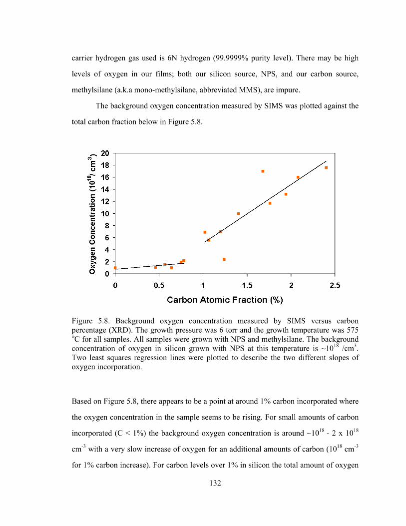
The background oxygen concentration measured by SIMS was plotted against the
total carbon fraction below in Figure 5.8.
Figure 5.8. Background oxygen concentration measured by SIMS versus carbon percentage (XRD). The growth pressure was 6 torr and the growth temperature was 575 oC for all samples. All samples were grown with NPS and methylsilane. The background concentration of oxygen in silicon grown with NPS at this temperature is ~1018 /cm3. Two least squares regression lines were plotted to describe the two different slopes of oxygen incorporation.
Based on Figure 5.8, there appears to be a point at around 1% carbon incorporated where
the oxygen concentration in the sample seems to be rising. For small amounts of carbon
incorporated (C < 1%) the background oxygen concentration is around ~1018 - 2 x 10¹⁸
cm-3 with a very slow increase of oxygen for an additional amounts of carbon (1018 cm-3
for 1% carbon increase). For carbon levels over 1% in silicon the total amount of oxygen

133
incorporated is then increasing at a faster rate, with the total amount of carbon
incorporated (13 * 1018 for 1% carbon increase). We would like to determine reason for
the two different slopes and why oxygen increases when more carbon is incorporated.
Unlike Si1-xGex where addition germanium enhances desorption of hydrogen, (which
leads to more open sites and hence oxygen incorporation), carbon does not have this
effect [5.22]. We would like to determine if this increase in oxygen is due to the impure
NPS source, the methylsilane source, or some other effect. We will attribute the “other
effect” as a carbon-related surface effect. We now add a plot of methylsilane partial
pressure and NPS partial pressure versus the carbon percentage on the secondary y-axis,
shown in Figure 5.9 below:
Figure 5.9. Oxygen concentration (solid squares) measured by SIMS vs. carbon atomic fraction (SIMS). The corresponding methylsilane (MMS) (blue open squares) and NPS (orange open squares) are plotted on the secondary y-axis. The growth pressure was 6 torr and the growth temperature was 575 oC for all samples.
134
From the plot we observe that the oxygen concentration (solid squares) is not
highly correlated to the NPS partial pressure (orange open squares). It is evident that
there is more of a relation between the oxygen concentration and the MMS partial
pressure (blue open squares), although there is still some variance among the sample
points. This may be due to the fact that the samples have slightly different growth rates.
Since neither the impurities from the NPS or the MMS gas sources can account fully for
the oxygen concentration, this implies that there is also surface effect due carbon that
causes additional adsorption of oxygen. We will plot the adsorption rate of oxygen onto
the Si:C surface. We make the assumption that the adsorption rate (AOxygen) is equivalent
to the incorporation rate, which is the oxygen concentration times the growth rate. At our
temperatures and partial pressures oxygen is stable on a silicon surface (i.e. oxygen does
not desorb) [1.6]. The adsorption rate is the amount of oxygen that lands on the surface.
The oxygen will come from the source and carrier gases (i.e. hydrogen, MMS and NPS).
The amount that adsorbs will be proportional to the sticking coefficient. The sticking
coefficient may be a function of the carbon concentration in the film, since the silicon
oxygen bond and a carbon oxygen bond have different bond enthalpies.
We plot the adsorption rate of oxygen in Figure 5.10 below and tabulate the
results in Table 5.3.
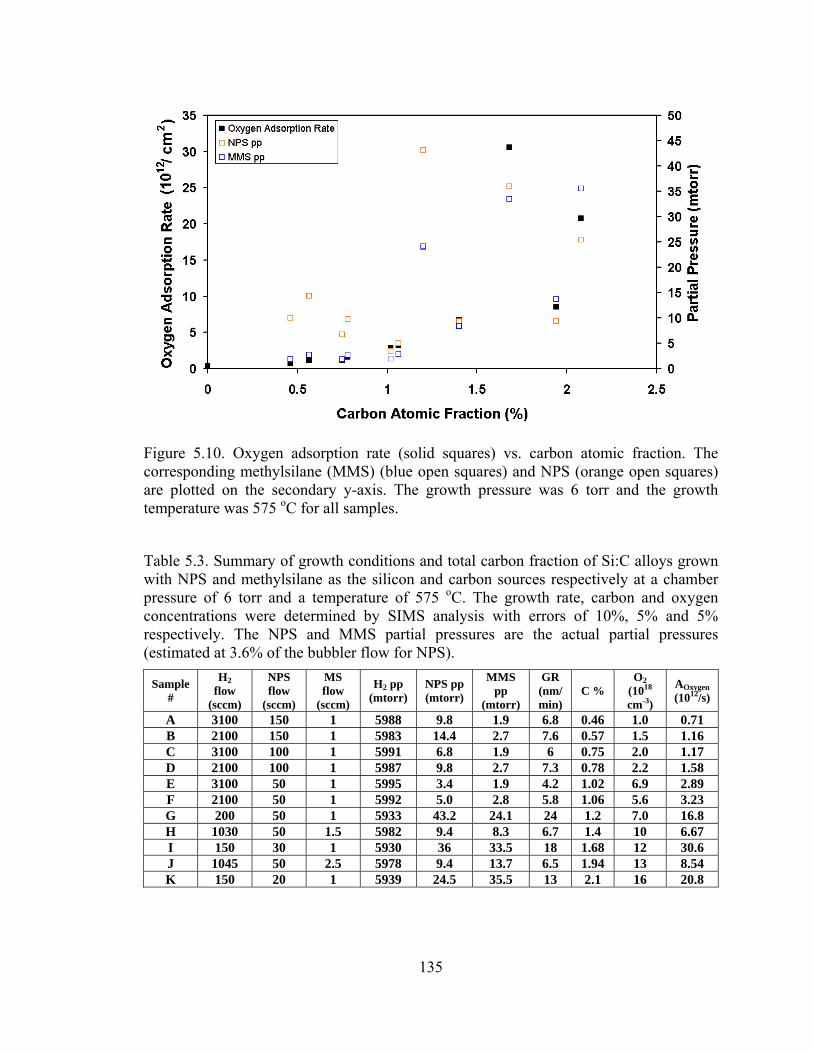
135
Figure 5.10. Oxygen adsorption rate (solid squares) vs. carbon atomic fraction. The corresponding methylsilane (MMS) (blue open squares) and NPS (orange open squares) are plotted on the secondary y-axis. The growth pressure was 6 torr and the growth temperature was 575 oC for all samples.
Table 5.3. Summary of growth conditions and total carbon fraction of Si:C alloys grown with NPS and methylsilane as the silicon and carbon sources respectively at a chamber pressure of 6 torr and a temperature of 575 oC. The growth rate, carbon and oxygen concentrations were determined by SIMS analysis with errors of 10%, 5% and 5% respectively. The NPS and MMS partial pressures are the actual partial pressures (estimated at 3.6% of the bubbler flow for NPS).
Sample #
H2 flow
(sccm)
NPS flow
(sccm)
MS flow
(sccm)
H2 pp (mtorr)
NPS pp (mtorr)
MMS pp
(mtorr)
GR (nm/min)
C % O2
(1018 cm-3)
AOxygen (1012/s)
A 3100 150 1 5988 9.8 1.9 6.8 0.46 1.0 0.71 B 2100 150 1 5983 14.4 2.7 7.6 0.57 1.5 1.16 C 3100 100 1 5991 6.8 1.9 6 0.75 2.0 1.17 D 2100 100 1 5987 9.8 2.7 7.3 0.78 2.2 1.58 E 3100 50 1 5995 3.4 1.9 4.2 1.02 6.9 2.89 F 2100 50 1 5992 5.0 2.8 5.8 1.06 5.6 3.23 G 200 50 1 5933 43.2 24.1 24 1.2 7.0 16.8 H 1030 50 1.5 5982 9.4 8.3 6.7 1.4 10 6.67 I 150 30 1 5930 36 33.5 18 1.68 12 30.6 J 1045 50 2.5 5978 9.4 13.7 6.5 1.94 13 8.54 K 150 20 1 5939 24.5 35.5 13 2.1 16 20.8

136
We compare samples with the same MS partial pressure and varying NPS partial
pressure. Comparing samples A, C, and E, we find that as the NPS partial pressure is
decreased from (9.8 to 6.8 then to 3.4 mtorr), the adsorption rate of oxygen is increasing.
The total background oxygen impurity level is decreasing since less NPS is used from
samples A to C to E, yet the adsorption rate is increasing in the same order. This indicates
that the carbon on the surface is increasing the oxygen sticking probability. While there is
more oxygen in the background for sample “A” then for sample “C”, less of the oxygen
is adsorbed onto the surface and incorporated. A comparison between B and D also leads
us to the same conclusion. We also note that the adsorption rate of oxygen is not directly
proportional to the carbon percentage. In Figure 5.10 above, we observe that the
adsorption rate increases with carbon fraction and is also dependent on the NPS and
MMS partial pressures. This indicates that more of the background oxygen is adsorbed
onto the surface and incorporated into the film as the carbon atomic fraction is increased.
Due to the varying gas flow condition of the samples and growth rates; it is difficult to
separate the contributions to the oxygen background from the three sources of oxygen
contamination (NPS, methylsilane, surface effect). This is due to the variance of the total
oxygen background impurities from NPS and MMS used in the samples. We write an
equation for the adsorption of oxygen onto the Si:C surface by splitting the adsorption of
oxygen on silicon sites and on carbon sites.
Eq. 5.2 1
(1 ) * *y y
nTotal Si CO y O k y O
−= − +
Where Ototal is the total oxygen adsorption rate, OSi and OC are the contributions from
adsorption on top a silicon surface site and carbon surface site respectively, y is the
carbon fraction, and kn is a scaling constant to account for the difference in the adsorption
rates, due to difference in the frequency of hydrogen desorption from a silicon site versus

137
a carbon site between a silicon site and a carbon site, and of order n., similar to the
difference in frequency of hydrogen desorption from a germanium site versus a silicon
site in SiGe films [5.23][5.24]. We can further separate the components based on the
impurities coming from MMS and NPS.
Eq. 5.3 1 1
(1 )[ ( ) ( )] * *[ ( ) ( )]y y y y
nTotal Si Si C CO y O NPS O MMS k y O NPS O MMS
− −= − + + +
Where OSi (NPS) is the oxygen adsorbed onto a silicon site due to oxygen from the NPS
source, OSi (MMS) is the oxygen adsorbed onto a silicon site due to oxygen form the
MMS source, OC (NPS) is the oxygen adsorbed onto a carbon site due to oxygen from the
NPS source, OC (MMS) is the oxygen adsorbed onto a carbon site due to oxygen form the
MMS source. Based on this equation, we can explain the good correlation between the
MMS pressure and oxygen adsorption into the film. Both the carbon atomic fraction and
the amount of oxygen adsorbed are dependent on the MMS source. This implies that for
good carbon growth a low oxygen impurity or purified MMS source is needed. Further
work and knowledge of the actual oxygen impurity concentrations of both the MMS and
NPS is needed to separate out the contributions due to each component and will not be
done in this thesis.
The effect of the growth rate and temperature on the amount of oxygen
incorporated into the films was next examined. We use a set of growth conditions which
all yield approximately 1% carbon. The methysilane silane flow rate was set to 1 sccm
and the flow through the NPS bubbler was set at 50 sccm for all samples. The plot of
these two sets of data are shown in Figure 5.11 below and tabulated in Table 5.4:

138
Figure 5.11. Background oxygen concentration (solid squares) measured by SIMS versus growth rate. The corresponding methylsilane (MS) partial pressure (open squares) was plotted on the secondary y-axis. The growth pressure was 6 torr and the growth temperature was 600 oC (blue) and 575 oC (orange). The carbon percentage for all samples is ~1%. The methylsilane silane flow rate was set to 1 sccm and the flow through the NPS bubbler was set at 50 sccm for all samples.
Table 5.4. Growth conditions of ~1% carbon atomic fraction in silicon at 575 oC and 600 oC, with NPS and MMS at 6 torr. The growth rate, carbon and oxygen concentrations were determined by SIMS analysis with errors of 10%, 5% and 5% respectively.
Temp H2
flow (sccm)
NPS flow
(sccm)
MS flow
(sccm)
H2 pp (mtorr)
NPS pp (mtorr)
MMS pp
(mtorr)
GR (nm/ min)
C % O2
(1018 cm-3)
AOxygen (1012/s)
575oC 3100 50 1 5995 3.4 1.9 4.2 1.02 6.9 2.89 575oC 2100 50 1 5992 5.0 2.8 5.8 1.06 5.6 3.23 600oC 3100 50 1 5995 3.4 1.9 8.5 0.98 19.0 16.2 600oC 2100 50 1 5992 5.0 2.8 9.2 1.02 10.5 9.71 600oC 1100 50 1 5985 9.4 5.4 18 1.17 7.9 14.3
Comparing the oxygen levels (Figure 5.11) at the two different growth temperatures of
575 oC (orange) and 600 oC (blue), it is evident that for carbon percentage, a reduction in
temperature also leads smaller amounts of oxygen incorporated even though the growth

139
rate is reduced. The adsorption rate of the oxygen (Table 5.4) is lower at the lower
temperature although the background impurity levels are the same (i.e. same NPS and
MMS partial pressures). There may be a higher surface concentration of carbon at the
higher temperatures leading to a higher adsorption rate of oxygen, and that not all of the
carbon is incorporated (i.e. surface segregation of carbon [5.25]). This could explain the
variance and lack of dependence of the adsorption rate on the MMS and NPS partial
pressures. The concentration of carbon of the surface is different for the samples even
though the amount incorporated is ~1% atomic fraction. Surface segregation effects are
covered in detail in chapter 7. The data implies that lower growth temperatures are better
for background oxygen concentrations in Si:C alloy epitaxial layers. As the growth rate is
increased the amount of oxygen incorporated into the film is also decreased. We would
like to note that the meythlsilane partial pressure does not correlate with the oxygen
concentration (for a set carbon concentration), indicating that a high growth rate can
reduce the effect of oxygen contamination coming from the methylsilane. This reduction
is not due to a decrease in adsorption rate of oxygen on the surface but by decreasing the
amount incorporated by increasing the growth rate.
We conclude that the higher the growth rate and the lower the temperature, the
lower background oxygen in the Si:C epitaxy. The oxygen is probably coming from
impure methylsilane and NPS sources and the adsorption in enhanced on a Si:C surface.
140
5.5 Si:C Alloy Epitaxial Layers Grown with Disilane and
Methylsilane
5.5.1 Growth of Si:C Epitaxial Layers Using Disilane and Methylsilane
Si:C alloy epitaxial layers were also grown on Si (100) wafers in our reactor
system using disilane as the silicon source and methylsilane as the carbon source. This
allows for the comparison of two different silicon precursors (disilane and NPS). We can
then determine how much of an effect the higher growth rate has on carbon
incorporation. The use of disilane and methylsilane to grow Si:C alloy epitaxial layers
has also been done by a previous student using 625 oC and 6 torr as the growth
temperature and chamber pressure respectively, and their results are well documented in
references [5.19][5.26]. We grow Si:C alloy epitaxial layers at 575 oC and 6 torr pressure,
to compare the layers with those grown using NPS as the silicon source.
Our disilane source is 10% disilane in hydrogen. The methylsilane source is 5%
methylsilane in hydrogen. The actual disilane flow was set to 10 sccm and hydrogen
carrier flow was set to 3 slpm, the methylsilane flow was varied. The XRD of the layers
grown are shown in Figure 5.12 below and summarized in Table 5.5:
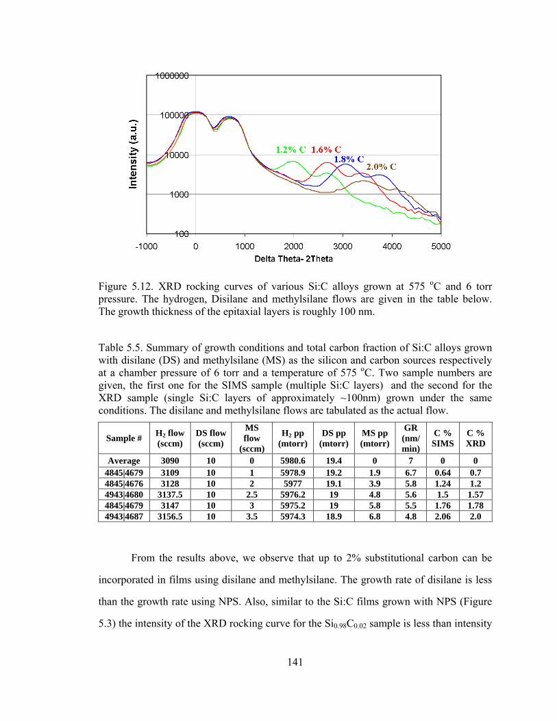
141
Figure 5.12. XRD rocking curves of various Si:C alloys grown at 575 oC and 6 torr pressure. The hydrogen, Disilane and methylsilane flows are given in the table below. The growth thickness of the epitaxial layers is roughly 100 nm.
Table 5.5. Summary of growth conditions and total carbon fraction of Si:C alloys grown with disilane (DS) and methylsilane (MS) as the silicon and carbon sources respectively at a chamber pressure of 6 torr and a temperature of 575 oC. Two sample numbers are given, the first one for the SIMS sample (multiple Si:C layers) and the second for the XRD sample (single Si:C layers of approximately ~100nm) grown under the same conditions. The disilane and methylsilane flows are tabulated as the actual flow.
Sample # H2 flow (sccm)
DS flow (sccm)
MS flow
(sccm)
H2 pp (mtorr)
DS pp (mtorr)
MS pp (mtorr)
GR (nm/min)
C % SIMS
C % XRD
Average 3090 10 0 5980.6 19.4 0 7 0 0 4845|4679 3109 10 1 5978.9 19.2 1.9 6.7 0.64 0.7 4845|4676 3128 10 2 5977 19.1 3.9 5.8 1.24 1.2 4943|4680 3137.5 10 2.5 5976.2 19 4.8 5.6 1.5 1.57 4845|4679 3147 10 3 5975.2 19 5.8 5.5 1.76 1.78 4943|4687 3156.5 10 3.5 5974.3 18.9 6.8 4.8 2.06 2.0
From the results above, we observe that up to 2% substitutional carbon can be
incorporated in films using disilane and methylsilane. The growth rate of disilane is less
than the growth rate using NPS. Also, similar to the Si:C films grown with NPS (Figure
5.3) the intensity of the XRD rocking curve for the Si0.98C0.02 sample is less than intensity
142
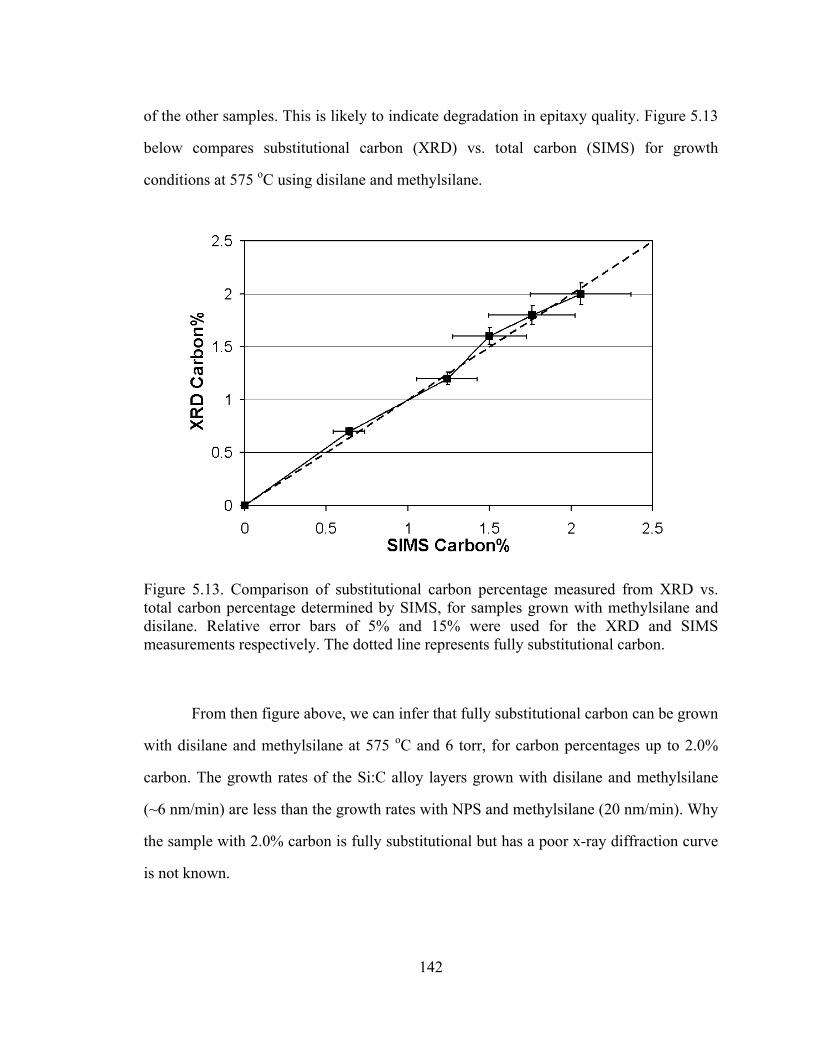
of the other samples. This is likely to indicate degradation in epitaxy quality. Figure 5.13
below compares substitutional carbon (XRD) vs. total carbon (SIMS) for growth
conditions at 575 oC using disilane and methylsilane.
Figure 5.13. Comparison of substitutional carbon percentage measured from XRD vs. total carbon percentage determined by SIMS, for samples grown with methylsilane and disilane. Relative error bars of 5% and 15% were used for the XRD and SIMS measurements respectively. The dotted line represents fully substitutional carbon.
From then figure above, we can infer that fully substitutional carbon can be grown
with disilane and methylsilane at 575 oC and 6 torr, for carbon percentages up to 2.0%
carbon. The growth rates of the Si:C alloy layers grown with disilane and methylsilane
(~6 nm/min) are less than the growth rates with NPS and methylsilane (20 nm/min). Why
the sample with 2.0% carbon is fully substitutional but has a poor x-ray diffraction curve
is not known.
143
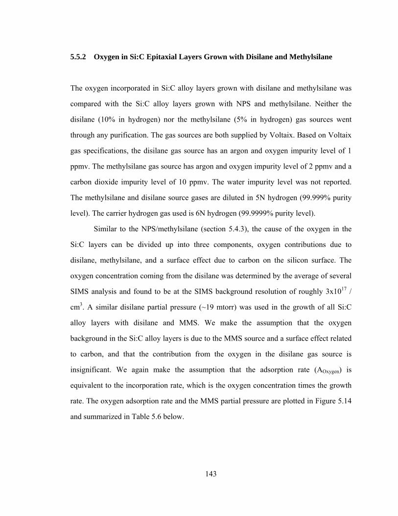
5.5.2 Oxygen in Si:C Epitaxial Layers Grown with Disilane and Methylsilane
The oxygen incorporated in Si:C alloy layers grown with disilane and methylsilane was
compared with the Si:C alloy layers grown with NPS and methylsilane. Neither the
disilane (10% in hydrogen) nor the methylsilane (5% in hydrogen) gas sources went
through any purification. The gas sources are both supplied by Voltaix. Based on Voltaix
gas specifications, the disilane gas source has an argon and oxygen impurity level of 1
ppmv. The methylsilane gas source has argon and oxygen impurity level of 2 ppmv and a
carbon dioxide impurity level of 10 ppmv. The water impurity level was not reported.
The methylsilane and disilane source gases are diluted in 5N hydrogen (99.999% purity
level). The carrier hydrogen gas used is 6N hydrogen (99.9999% purity level).
Similar to the NPS/methylsilane (section 5.4.3), the cause of the oxygen in the
Si:C layers can be divided up into three components, oxygen contributions due to
disilane, methylsilane, and a surface effect due to carbon on the silicon surface. The
oxygen concentration coming from the disilane was determined by the average of several
SIMS analysis and found to be at the SIMS background resolution of roughly 3x10¹⁷ /
cm3. A similar disilane partial pressure (~19 mtorr) was used in the growth of all Si:C
alloy layers with disilane and MMS. We make the assumption that the oxygen
background in the Si:C alloy layers is due to the MMS source and a surface effect related
to carbon, and that the contribution from the oxygen in the disilane gas source is
insignificant. We again make the assumption that the adsorption rate (AOxygen) is
equivalent to the incorporation rate, which is the oxygen concentration times the growth
rate. The oxygen adsorption rate and the MMS partial pressure are plotted in Figure 5.14
and summarized in Table 5.6 below.
144
Figure 5.14. Oxygen adsorption rate (black solid squares) is plotted vs. carbon atomic percentage. The calculated oxygen adsorption rate (orange solid squares) is also plotted. The MMS partial pressure (blue open squares) is plotted on the secondary y-axis. All samples were grown at 575 oC and 6 torr, with 3 slpm hydrogen carrier and 10 sccm disilane flow.
Table 5.6. Summary of growth conditions and total carbon fraction of Si:C alloys grown with disilane (DS) and methylsilane (MS) as the silicon and carbon sources respectively at a chamber pressure of 6 torr and a temperature of 575 oC. The growth rate and oxygen concentrations are determined by SIMS analysis. The oxygen contributions from disilane, methylsilane, and the surface were calculated using the method described in the text above.
Sample H2 flow (sccm)
Si2H6 flow
(sccm)
MMS flow
(sccm)
H2 pp (mtorr)
Si2H6 pp
(mtorr)
MMS pp
(mtorr)
GR (nm/min)
C % O2
(1018 cm-3)
AOxygen (1012/s
) Average 3090 10 0 5980.6 19.4 0 7 0 0.3 0.21
4845|4679 3109 10 1 5978.9 19.2 1.9 6.7 0.64 1.0 0.67 4845|4676 3128 10 2 5977 19.1 3.9 5.8 1.24 2.4 1.41 4943|4680 3137.5 10 2.5 5976.2 19 4.8 5.6 1.5 9.0 5.04 4845|4679 3147 10 3 5975.2 19 5.8 5.5 1.76 11.7 6.44 4943|4687 3156.5 10 3.5 5974.3 18.9 6.8 4.8 2.06 19.1 9.12
As shown in Figure 5.14 we observe a trend of increasing oxygen concentration along
with increasing carbon atomic percentage, similar to that observed with NPS and
methylsilane. We find that the oxygen adsorption rate is increasing faster than linear

145
while the MMS partial pressure is increasing linearly. We use Equation 5.3, and set the
oxygen contribution from disilane to zero and assume that the oxygen contribution from
the silicon site is small compared to that from the carbon site. We rewrite Equation 5.3 as
Equation 5.4 below:
Eq. 5.4 1 1
(1 )[ ( ) ( )] * *[ ( ) ( )]y y y y
nTotal Si Si C CO y O DS O MMS k y O DS O MMS
− −= − + + +
=> * *[ ( )]y
nTotal CO k y O MMS=
We plot the calculated oxygen adsorption rate using a scaling factor, kn of
4x10¹¹/(cm2*mtorr) with order 1.6. We do not understand the physics behind this result
or whether 1.6 is the correct order. We find that the calculated result (plotted in Figure
5.14 above) is within error bars of the actual oxygen adsorption rate. The calculated
oxygen adsorption rate is done to illustrate that there is a effect of carbon atoms on the
surface that is increasing the oxygen adsorption rate. We do not understand why carbon
increases the oxygen adsorption rate. One possibility is that the carbon-oxygen bond is
stronger than the silicon-oxygen bond. Another possibility is that the surface becomes
more disordered (i.e. loses its 2x1 reconstruction, similar to limited epitaxy thickness),
allowing for an increase in oxygen adsorption onto the surface. We find that the oxygen
adsorption rates in Si:C alloy layers grown with NPS and MMS and the oxygen
adsorption rates in Si:C alloy layers grown with disilane and MMS are all on the order of
1012 / cm2, in spite of much higher impurity levels in the NPS and MMS. This suggests
that the amount of carbon on the surface is different for the two higher-order silanes (i.e.
a different amount of carbon is incorporated and segregated back to the surface).
146
5.6 Si:C Alloy Epitaxial Layers Grown with NPS and
Methylchloride
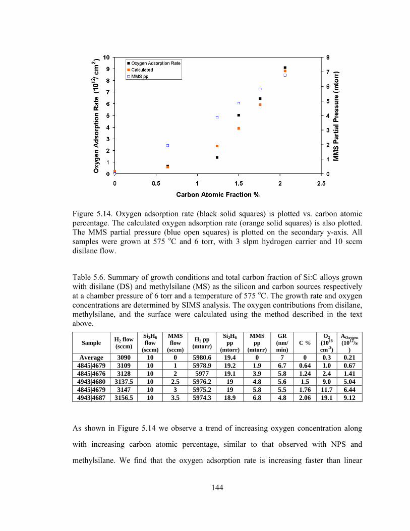
Si:C alloy epitaxy growth was also investigated upon using methylchloride (also known
as chloromethane, CH3Cl) as the carbon source. The reason we tried methylchloride was
that it might be easier to achieve selective Si:C epitaxy, due to the chlorinated chemistry
of methylchloride. The results are shown in Figure 5.15 below and summarized in Table
5.7:
Figure 5.15. XRD rocking curves of various Si:C alloys grown at different temperatures using NPS and methylchloride as the silicon and carbon sources respectively. The NPS flow was 100sccm and the methylchloride flow was 15 sccm. The temperatures were varied from 575 oC to 675 oC in 25 oC increments. The target growth thickness of the Si:C epitaxial layers is 100 nm.
147
Table 5.7. Summary of Si:C alloys grown with NPS and methylchloride as the silicon and carbon sources respectively
Growth Temperature
Carbon % (XRD)
Hydrogen (sccm)
NPS (sccm) Methylchloride (sccm)
Growth Rate (nm/min)
575 ? 3000 100 15 8 600 1.2 3000 100 15 14 625 1.35 3000 100 15 25 650 1.7 3000 100 15 50 675 1.85 3000 100 15 100
Using methylchloride and NPS, there was no peak related to Si1-yCy observed for
layers grown at 575 oC. There is a small and broad carbon peak at 600 oC. The peak
observed at 600 oC is well resolved and right of the peak observed at 625 oC. Increasing
the temperature to 650 oC peak shifts to the right again, indicating a higher carbon
fraction. A very broad carbon peak is observed for growth of Si1-yCy layers at 675 oC.
Comparing peak intensities we observe that the intensity increases from 600 oC to 625 oC, and then decreases subsequently by increasing the temperature. The latter decrease in
intensity going from 625 oC and upward could be attributed to the fact that the carbon
may not be fully substitutional and the layers were degraded. The fact that the 600 oC
intensity is not as high as the 625 oC intensity was surprising. It is possible that the
methylchloride molecule was not cracking sufficiently at the lower temperatures, and
therefore inhibited the growing surface, leading to thinner layers. The thinner Si:C layers
may not have been resolved by the XRD scans. In conclusion, there exists only a small
growth window for Si:C using methylchloride as the carbon source. At low temperatures
we may not be able to incorporate carbon as the molecule may not be cracking; at high
temperatures we may be unable to incorporate the carbon without degrading the epitaxial
layers. We conclude that methylchloride is not a good source for the growth of Si1-xCx
layers.
148
5.7 Summary
The technique for the incorporation of Si1-yCy alloys with dilute carbon fractions in
silicon epitaxial layers are discussed in this chapter. X-ray diffraction and Vegard’s law
was used to determine the substitutional amount of carbon. High quality Si1-yCy alloys
layers were achieved using a neopentasilane as silicon source with methylsilane. Very
high growth rates of Si1-yCy alloys of 18nm/min and 13nm/min for fully substitutional
carbon levels of 1.8% and 2.1%, respectively, were achieved. The highest substitutional
carbon level achieved was 2.65% (strained perpendicular lattice constant of 5.347Å) as
determined by X-ray diffraction. Si:C alloys were grown using two different silicon
sources (NPS and disilane) and two different carbon sources (methylsilane and
methylchloride). Oxygen levels in Si:C epitaxy layers are examined. The primary cause
of the oxygen background appears to be coming from the methylsilane source, although a
part of it may be due to a surface effect related to carbon. Based on background oxygen
levels, our data suggests that high growth rates, lower temperatures, and cleaner
methylsilane and silicon sources are desirable for Si:C epitaxy layers with reduced
oxygen concentrations.

149
Chapter 6
Low Temperature In-Situ Surface
Cleaning by Etching of Silicon, and
Selective Silicon and Silicon-Germanium
Epitaxy
6.1 Introduction to Low Temperature In-Situ Surface
Cleaning
In order to have good quality epitaxy, the starting surface must be free of surface
contaminants. It is quite difficult to begin with a silicon surface that is free of impurities.
After any chemical cleaning before growth the silicon wafer must first be transferred
from the air into the reactor chamber. The chemicals and water may have impurities. The
air is also filled with unwanted impurities that can adhere to the surface of the wafer,
such as moisture, oxygen, and carbon.
To remove these impurities, thermal baking in hydrogen at high temperatures (T >
1000 oC) was conventionally used in CVD for in-situ cleaning. Oxygen on the silicon
surface is desorbed via the following reaction: [6.1]
Eq. 6.1 SiO2 + H2 => SiO (g) + H2O

150
An HF dip to remove the native oxide and passivate the surface with hydrogen has been
shown to significantly reduce the oxygen and carbon at the interface between a silicon
substrate and epitaxial layer [6.2]. However, there are still trace amounts of these
contaminants on the surface (~1013 cm-2) [6.3]. Thermal baking in hydrogen at
temperatures of around 750-800 oC were still necessary to remove these remaining trace
contaminants [6.4][6.5]. With novel source gases such as trisilane and neopentasilane,
reasonable epitaxy growth rates at low temperature have been achieved. However,
cleaning steps still require a temperature greater than 750 oC, limiting the thermal budget
of the growth process. In this chapter we will examine a novel surface cleaning
technique: etching of the top silicon (or SiGe) surface layer with chlorine, which should
remove the unwanted impurities from the surface.
6.2 In-situ Silicon Etchants
Thermal etching of silicon in-situ in epitaxial reactors is typically done using
hydrogen chloride (HCl) in a hydrogen ambient at temperatures above 800 oC. For
temperatures less than 750 oC, the etch rates with HCl have been observed to be less than
1nm/min [6.6]. (It has been shown however, that SiGe surfaces can be etched with HCl at
temperatures of 625 oC [6.6]. This is believed to be due to the enhanced desorption of
hydrogen from SiGe surfaces, which allows for the adsorption of the HCl) The
mechanism by which silicon is etched by HCl is given in Equation 6.2 below:
Eq. 6.2 Si (s) + 2HCl (g) => SiCl2 (g) + H2 (g)
Previously attempts have been made to use chlorine instead of hydrogen chloride to etch
silicon in a hydrogen ambient [6.7]. It was observed that the etch rate was still negligible

151
below 750 oC. The authors believed that the hydrogen carrier gas was reacting with the
chlorine to form HCl, inhibiting any improvement of etch rates from using Cl2 as the
etchant.
Our silicon etching experiments were done using a flow of 15 sccm of chlorine
gas with a flow of 3 slpm of hydrogen gas, set at a chamber pressure of 6 torr with varied
temperatures. Etch rate experiments were done on silicon wafers with patterned silicon
dioxide. The etch rate was determined by step height measurements between the silicon
and the silicon dioxide surface patterns. The etch rate of the silicon dioxide was found to
be negligible for the temperature range of 500 oC – 1000 oC (measured to be less than 10-
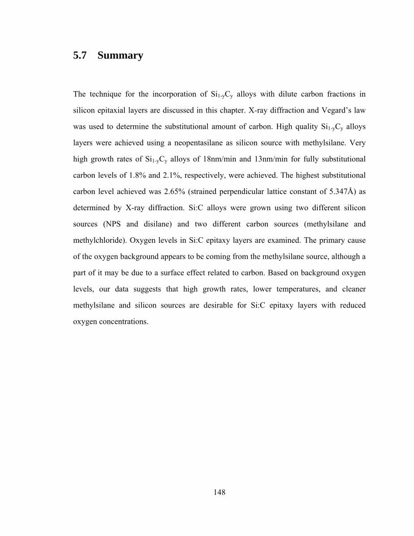
2 nm/min). At high temperatures 900 oC and 1000 oC, the silicon etch rates were
35nm/min and 220nm/min respectively. Negligible etch rates (less than 0.1 nm/min) of
silicon using chlorine in hydrogen at 575 oC and 600 oC were observed in our lab
consistent with other authors [6.7]. The etch rates of HCl and Cl2 in hydrogen are plotted
in Figure 6.1 below. From Figure 6.1 below, we can observe that etching with chlorine in
a hydrogen ambient offers little improvement over etching with HCl in hydrogen.
152
Figure 6.1. Etch rates of chlorine and HCl in hydrogen ambient. The chlorine in hydrogen (orange) data is from experiments conducted in our lab at a chamber pressure of 6 torr, with a flow of 15 sccm of chlorine gas and a flow of 3slpm of nitrogen gas. At 600 oC, the etch rate was less than 0.1 nm/min. HCl data is from reference 6.6 and the chlorine in hydrogen (blue) is from reference 6.7.
6.3 Silicon Etching with Chlorine in a Nitrogen Ambient
6.3.1 Etch Rates
To prevent chlorine from reacting with hydrogen, we used a nitrogen ambient
instead of a hydrogen ambient for the thermal etching of silicon with chlorine. The
surface reaction by which chlorine etches silicon is given by the following Equation 6.3:
Eq. 6.3 Si(s) + Cl2 => SiCl2 (g) [6.8]
153
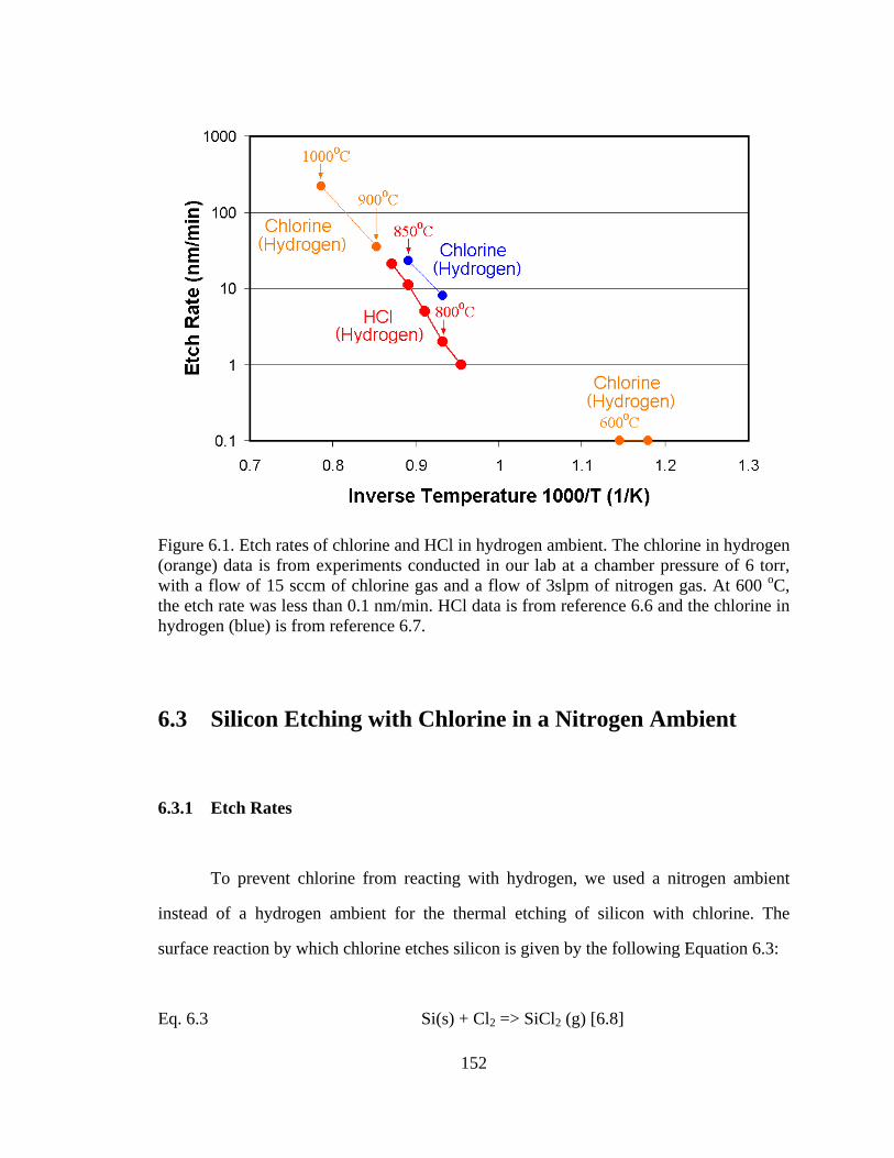
A partial pressure of 6 torr of nitrogen and 30 mtorr of chlorine was used in our
experiments. Etch rates of 11nm/min, 5nm/min, and 1nm/min were achieved at 575 oC,
550 oC, and 525 oC respectively. The etch rates are plotted versus temperature in Figure
6.2 below.
Figure 6.2. Chlorine etch rates (nm/min) vs. inverse temperature. The etch rates are measured by step height measurements. The chamber pressure is set to 6 torr, with 3 slpm of nitrogen carrier flow and 15 sccm Cl2 gas flow.
Using an etch temperature of 575 oC, the etch rate was measured as a function of chlorine
flow rates while holding the nitrogen flow and chamber pressure constant at 3 slpm and 6
torr respectively. The results are plotted in Figure 6.3 below.

154
Figure 6.3. Silicon etch rates versus chlorine flow in nitrogen ambient at 575 oC and 6 torr chamber pressure.
The etch rate first increases linearly with the chlorine flow, and then increases at a slower
rate. The rate is still increasing with the flow rate at 120 sccm, indicating that even faster
etch rates may still be achievable. We would like to note that the chlorine etch rate (10-30
nm/min) in nitrogen can exceed the growth rates of silicon using both NPS and trisilane
at 575 oC [6.9][6.10]. This is important for further selective epitaxy applications where
the ability to etch away a nucleated surface layer on oxide is vital.
6.3.2 Surface Roughness After Etching
Smooth surfaces are desirable prior to the start of epitaxy. Surface roughness
leads to the deterioration in the breakdown voltage of gate oxides [6.11]. Impurities on
the surface need to be removed without roughening the surface. The surface roughnesses
of the etched silicon surfaces were examined using AFM. The results are shown in Figure
6.4 below:

155
Figure 6.4. RMS surface roughness versus etch time using 15 sccm of chlorine gas in nitrogen ambient at 575 oC and 6 torr chamber pressure.
As the surface being etched, surface roughness increases over time. To keep the
roughness under ~ 1nm RMS, only small etch times (< 2 minutes) can be used in order to
minimize surface roughening. The AFM scan of a sample etched for 2 min with 1nm
RMS roughness is shown in Figure 6.5 below:
Figure 6.5. AFM image of silicon surface after etching of 20nm of silicon at 575 oC and a pressure of 6 torr with a flow of 15 sccm of chlorine. RMS surface roughness is ~ 1nm
156
6.4 Silicon Surface Cleaning by Etching
6.4.1 Oxygen and Carbon Impurity Removal via Etching
The effectiveness of the chlorine etching for cleaning a silicon surface prior to
epitaxy was examined. SIMS was done to compare the interface impurity concentration
after silicon epitaxy that had no in-situ clean step with that after epitaxy that had a 575 oC
chlorine etch step. Prior to silicon growth in both steps, the sample was cleaned with a
conventional ex-situ wet clean of H2SO4/H2O2 and a dilute HF dip [6.4]. The silicon
epitaxial layer was grown in this experiment at 700 oC at 6 torr chamber pressure using
dichlorosilane (DCS) as the silicon source. A 2.5-nm boron doping marker was used to
indicate the start of silicon epitaxy in both cases. Both experiments were performed on a
single wafer so data could be obtained with a single SIMS measurement. After the first
wet cleaning the sample was loaded into the reactor in a hydrogen environment. The
temperature was raised to 700 oC and approximately 150 nm of silicon was grown,
without any cleaning steps such as an intentional hydrogen bake. (The wafer was at 700 oC for about 15 seconds before the DCS was turned on to start the growth.) The wafer
was then taken out of the reactor and exposed to air for 12 hours. Now the sample was
chemically cleaned again as described earlier. After loading the sample was then heated
to 575 oC in hydrogen ambient, using a hydrogen flow of 3 slpm. The hydrogen was then
turned off and nitrogen was turned on to the same flow rate. Then using a flow of 15
sccm of chlorine with a flow of 3 slpm of nitrogen gas at 575 oC and 6 torr, we etched of
approximately 20 nm of silicon prior to the start of epitaxial growth. After etching, the
ambient was switched back to hydrogen, the temperature was then raised from 575 oC to
700 oC and 50 nm of silicon was grown. From the SIMS shown in Figure 6.6, we
observed an interfacial spike in both oxygen and carbon levels for the growth with no
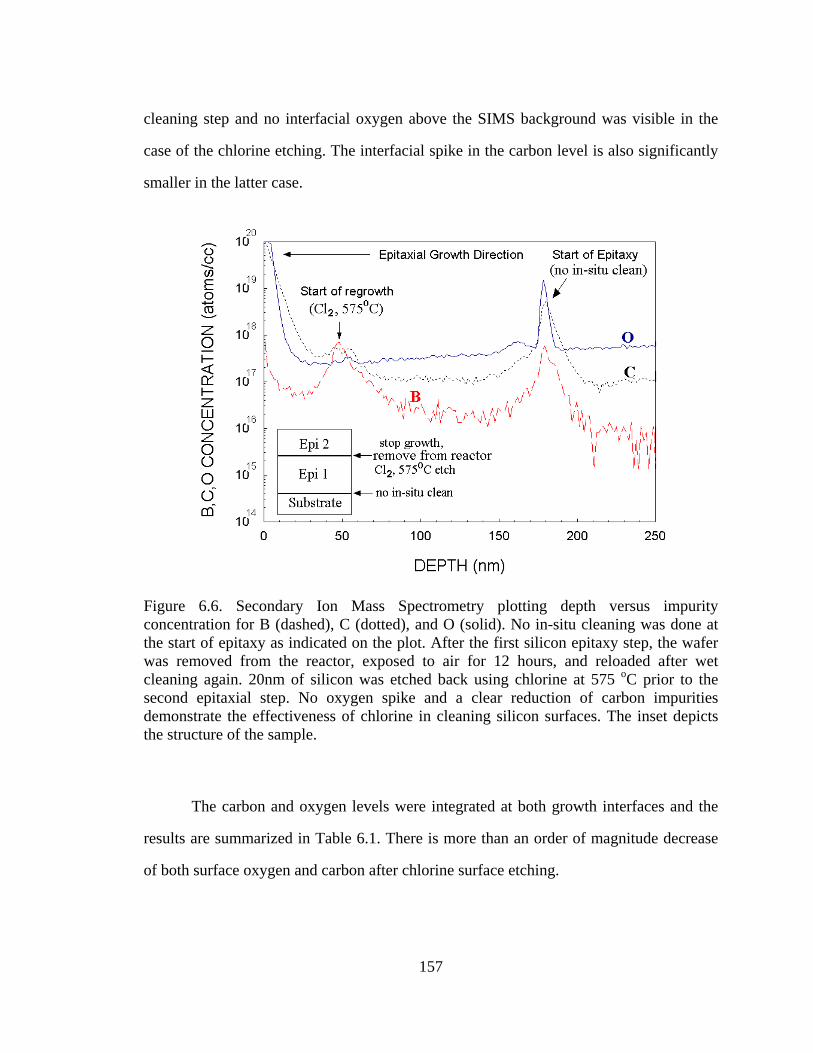
157
cleaning step and no interfacial oxygen above the SIMS background was visible in the
case of the chlorine etching. The interfacial spike in the carbon level is also significantly
smaller in the latter case.
Figure 6.6. Secondary Ion Mass Spectrometry plotting depth versus impurity concentration for B (dashed), C (dotted), and O (solid). No in-situ cleaning was done at the start of epitaxy as indicated on the plot. After the first silicon epitaxy step, the wafer was removed from the reactor, exposed to air for 12 hours, and reloaded after wet cleaning again. 20nm of silicon was etched back using chlorine at 575 oC prior to the second epitaxial step. No oxygen spike and a clear reduction of carbon impurities demonstrate the effectiveness of chlorine in cleaning silicon surfaces. The inset depicts the structure of the sample.
The carbon and oxygen levels were integrated at both growth interfaces and the
results are summarized in Table 6.1. There is more than an order of magnitude decrease
of both surface oxygen and carbon after chlorine surface etching.

158
Table 6.1. Integrated carbon and oxygen levels for both the no in-situ clean and
chlorine cleaning at 575 oC
In-Situ Clean Integrated Oxygen
Concentration
Integrated Carbon
Concentration
None 8x10¹² atoms/cm2 3x10¹² atoms/cm2
575oC Cl2 etch < 1011 atoms/cm2 < 2x10¹¹ atoms/cm2
6.4.2 Phosphorus Impurity Removal via Etching
Experiments were done to test the ability of chlorine surface etching steps to
remove other surface impurities, specifically phosphorus. Phosphorus as an impurity is
extremely efficient at sticking on silicon surfaces and difficult to remove [6.12][6.13]. To
remove phosphorus from the surface of silicon, high temperature thermal desorption is
required [6.14]. Phosphorus is known to ride up onto the growing layer (surface
segregation), leading to poor doping transitions when the phosphine source gas is turned
off during silicon epitaxy. This effect is modeled in detail in chapter 7. We attempt to
remove the surface phosphorus layers to avoid surface segregation effects.
To determine the effectiveness of the silicon etching in the removal of
phosphorus, a thermal desorption step at 800 oC, a chlorine surface cleaning step by
etching at 575 oC, and no in-situ cleaning were compared. Silicon was grown in this
experiment at 700 oC at 6 torr chamber pressure using dichlorosilane (DCS) as the silicon
source in hydrogen ambient. The growth was halted and a flow of 500 sccm of phosphine
gas (100ppm phosphine in hydrogen) was injected into the chamber with 3 slpm
hydrogen flow at a temperature of 700 oC at 6 torr chamber pressure for 5 minutes to coat
the surface with phosphorus.
For the first cleaning step, we attempted to remove the phosphorus from the surface
by etching with chlorine at 575 oC. Silicon was then grown and a thin SiGe layer was

159
then grown to reduce the surface concentration of phosphorus prior to the next phosphine
dose, followed by a second phosphine exposure. (The SiGe is effective at gettering the
surface phosphorous into the solid [6.15]) After the second phosphine dose, we attempted
to remove the phosphorus via desorption by heating the surface to 800 oC for 10 minutes
in 3 slpm hydrogen at 6 torr. Silicon was then grown followed by a thin SiGe layer to
reduce the surface concentration of phosphorus prior to the next phosphine dose,
followed by a final phosphine exposure. After the last phosphine dose, no cleaning step
was performed and more silicon was grown. At no time was the chamber opened or the
sample removed from the chamber during this experiment. A SIMS measurement of
dopants and impurities vs. depth is shown in Figure 6.7.
Figure 6.7. Secondary Ion Mass Spectrometry plotting depth versus impurity concentration for P (solid), C (dotted), and O (dashed). Growth was halted to cover the surface with phosphorus by injecting phosphine into the chamber at 3 different times during the growth. After the first two phosphine doses, different techniques were used to attempt to remove the phosphorus from the surface. SiGe layers were grown in between phosphorus doses to reduce the surface phosphorus concentration.

160
No phosphorus spike was observed at the interface treated with the chlorine
etching step, indicating that chlorine etching removed all of the phosphorus from the
surface prior to growth. A phosphorus spike at the growth interface after 800 oC thermal
treatment was still observed showing that the treatment was less effective than the
etching. The surface desorption of the remaining phosphorus led to a high concentration
in the top SiGe layer. (The spreading of the phosphorus from the first SiGe layer into the
substrate is possibly due to the annealing step at 800 oC). The last phosphorus spike,
without any cleaning step, is used as the control for comparison. At each interface the
phosphorus levels were integrated and are summarized in Table 6.2.
Table 6.2: Integrated phosphorus levels for no in-situ clean, chlorine cleaning at 575 oC, and 800 oC desorption.
In-Situ Clean Integrated Phosphorus Concentration
None 3x10¹² atoms/cm2
575oC Cl2 < 1011 atoms/cm2
800oC desorption 2x10¹² atoms/cm2
No significant reduction in phosphorus concentration was observed from the 800 oC desorption technique, which produced a decrease from 3x10¹²
atoms/cm2 to 2 x10¹²
atoms/cm2, while the Cl2 etching step reduced the phosphorus concentration significantly
from 3x10¹² atoms/cm2 to less than 1011 atoms/cm2. This indicates that the chlorine
etching of the silicon surface also etched away the phosphorus atoms that were adsorbed
onto the surface. Note, however that in the first and second cases a large amount of
phosphorus was gettered by the SiGe layer (2x10 12 / cm2 after the chlorine etch and
3x10¹³ / cm2 after the 800 oC desorption step). In the first case the background
phosphorus in the chamber accumulation was probably gettered by the SiGe. In the
second case, a large surface concentration of phosphorus was incorporated into the SiGe
layer from the phosphorus not removed by desorption at 800 oC.
161
6.5 Quality of Epitaxial Growth on Chlorine-Etched Surfaces
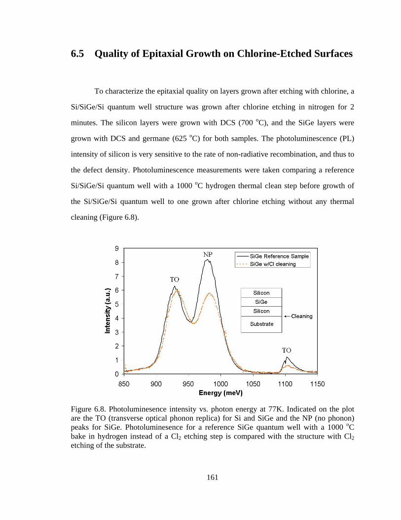
To characterize the epitaxial quality on layers grown after etching with chlorine, a
Si/SiGe/Si quantum well structure was grown after chlorine etching in nitrogen for 2
minutes. The silicon layers were grown with DCS (700 oC), and the SiGe layers were
grown with DCS and germane (625 oC) for both samples. The photoluminescence (PL)
intensity of silicon is very sensitive to the rate of non-radiative recombination, and thus to
the defect density. Photoluminescence measurements were taken comparing a reference
Si/SiGe/Si quantum well with a 1000 oC hydrogen thermal clean step before growth of
the Si/SiGe/Si quantum well to one grown after chlorine etching without any thermal
cleaning (Figure 6.8).
Figure 6.8. Photoluminesence intensity vs. photon energy at 77K. Indicated on the plot are the TO (transverse optical phonon replica) for Si and SiGe and the NP (no phonon) peaks for SiGe. Photoluminesence for a reference SiGe quantum well with a 1000 oC bake in hydrogen instead of a Cl2 etching step is compared with the structure with Cl2 etching of the substrate.

162
The SiGe layers were grown after the chlorine etch step. If chlorine etching had a
detrimental effect on the subsequent epitaxy, then all the layers after chlorine etching
would be of a poor crystalline quality. The comparable photoluminesence intensities of
SiGe and Si indicate high-quality defect-free silicon epitaxy growth on a chlorine-etched
surface.
6.6 Selective Silicon- Germanium Epitaxy
6.6.1 Techniques for Achieving Selective Epitaxial Growth
Selective epitaxy is the growth on epitaxy on patterned substrates, where epitaxy growth
occurs only on a crystalline silicon surface and does not grow on any other surface
(typically an oxide or nitride surface). This technique used to achieve raised-
source/drains and in certain epitaxial regrowth applications where only growth in certain
regions is desired [6.16]. Silicon will often grow even on the oxide/nitride surface after a
certain nucleation (incubation) period. The growth on a non-silicon surface (e.g. oxide)
would be either polysilicon or amorphous silicon. Selective epitaxy can be achieved three
different ways.
In the first (desired) case the nucleation period is long enough such that a
selective layer can be grown only on the crystalline silicon region. This requires an
extremely clean reactor system and high-vacuum conditions; unwanted surface
contamination leads to nucleation sites, which will reduce the nucleation time [6.17].
In the second case a silicon etchant (typically HCl) as injected at the same time of
growth. This technique achieves selective growth by either the prevention of a nucleation
layer from forming or by extending the nucleation time so that enough selective epitaxy

163
is achieved. The mechanism is that the chlorine leads to some etching occurring
simultaneous with growth. With chlorinated growth sources (such as DCS), often no
extra chlorinated etch gases sources such HCl is required. The etchant reduced the growth
rate.
The third case deposition /etch cycles are used. This technique is a cross between
the first and second techniques and is illustrated in Figure 6.9 below:
Figure 6.9. Growth thickness versus deposition time illustrating selective growth using deposition / etch cycles. The blue line is the net growth on a silicon surface and the orange line is the deposition on oxide.
Growth on both the silicon and on the oxide (arbitrary non-selective surface) occurs.
However, the growth on the oxide (orange line in Figure 6.9) does not occur right away
as it takes a certain amount of time (2 units in Figure 6.9) before a layer has nucleated.
During the nucleation time, silicon is constantly deposited on the crystalline surface
(blue). After the layer on oxide has grown a small amount (time at 3 units), the deposition

164
is halted and we proceed to etch both the crystalline silicon layer and the nucleation layer
(time form 3 to 4). The oxide surface is then removed of all nuclei, and we then proceed
to do deposition again. After each cycle the amount of “selective” epitaxy increases until
the desired amount is achieved.
6.6.2 Nucleation Time for SiGe on Oxide-Patterned Wafers
We will attempt to achieve selective epitaxy of SiGe on silicon (100) wafers w/ patterned
silicon dioxide using the deposition / etch cycle technique. The growth of SiGe was done
at a chamber pressure of 6 torr and growth temperature of 625 oC. The growth was
conducted in hydrogen ambient with hydrogen flow of 3 slpm. The flow of DCS was 26
sccm and the flow of germane was 100 sccm (0.8% germane in hydrogen). The growth
rate (non-selective) is 6 nm/min and the germane fraction is 20%. The SiGe nucleation
experiments were first conducted on patterned silicon wafers without the flow of the
etchant HCl. The pattern comprised of 30 micron silicon stripes and 100 micron oxide
stripes. The nucleation time was determined to be 12 minutes before any growth was
detected on the oxide using reflectance spectroscopy (Nanospec using the poly on oxide
program). A value of more than 10 Angstroms on the oxide was interpreted as deposition.
We then attempted to grow SiGe on RIE (reactive ion etching) etched trenches 20 nm in
width and 200nm apart and 55 nm in depth (Figure 6.10).
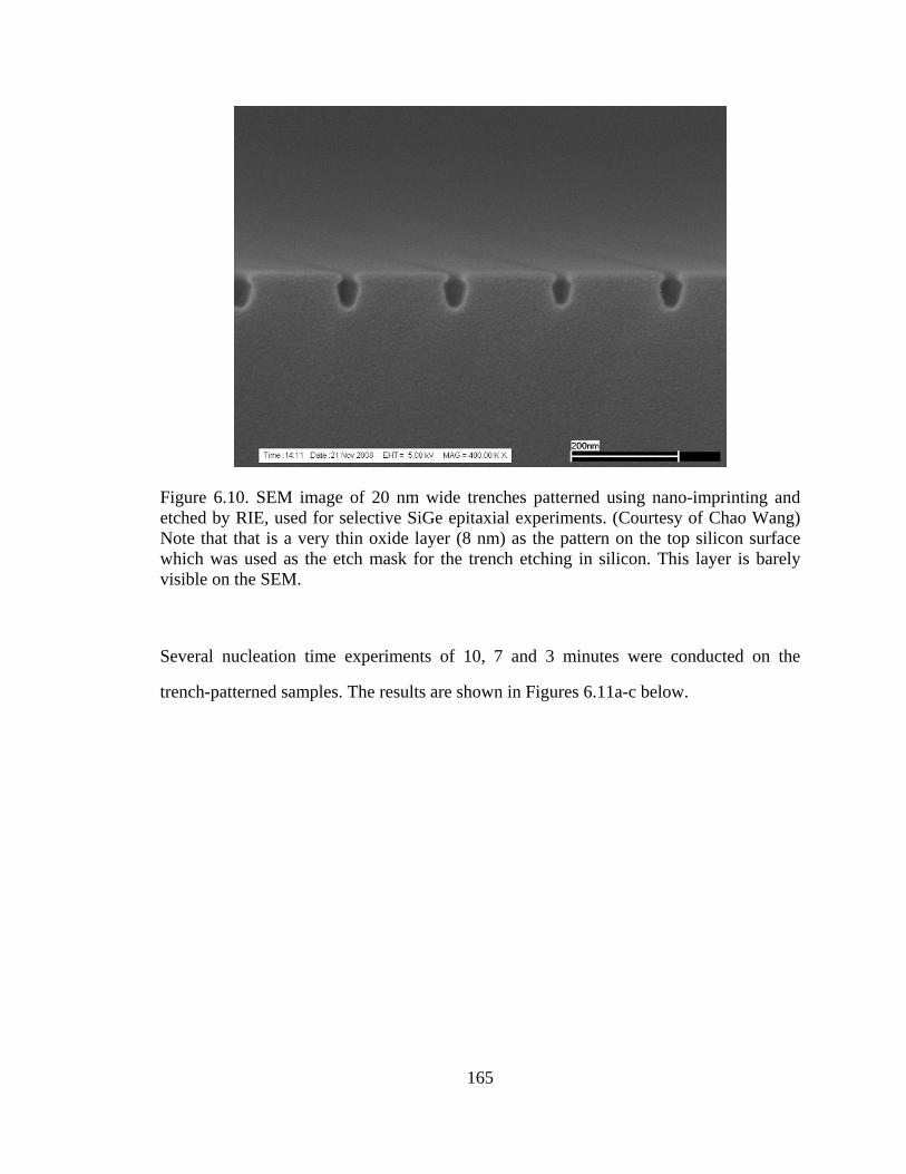
165
Figure 6.10. SEM image of 20 nm wide trenches patterned using nano-imprinting and etched by RIE, used for selective SiGe epitaxial experiments. (Courtesy of Chao Wang) Note that that is a very thin oxide layer (8 nm) as the pattern on the top silicon surface which was used as the etch mask for the trench etching in silicon. This layer is barely visible on the SEM.
Several nucleation time experiments of 10, 7 and 3 minutes were conducted on the
trench-patterned samples. The results are shown in Figures 6.11a-c below.

166
Figure 6.11a-c. SEM of a) 3 minute, b) 7 minute, c) 10 mintue, SiGe growth on RIE etched 20 nm wide trenches. We note the SiGe growth rate on the patterned sample is twice the non-selective (blanket) SiGe growth rate. The growth conditions are 6 torr chamber pressure, 625 oC, 3 slpm hydrogen, 26 sccm DCS and 100 sccm germane gas flows. The dotted circle in a) highlights the nucleation on the edges of the trench. The dotted white lines indicate the filled trench in b and c. SEM images courtesy of Chao Wang.

167
As shown in the three figures above, the nucleation time is approximately 3
minutes. We observe that nuclei begin at the edges of the trench starting at approximately
3 minutes. At the growth time is increased the nuclei coalesce, and is roughly 30 nm in
height in Figure 6.11b after a growth time of 7 minutes. The nuclei then coalesce into a
smooth layer after ten minutes of growth (Figure 6.11a).
To achieve selective epitaxial growth, we used the Cyclical Deposition and Etch
(CDE) method of Figure 6.9. HCl was used as the etchant and HCl etch rates were taken
from a paper [6.6]. It was shown that SiGe etch rates were much higher than the silicon
etch rates using HCl, due to the enhanced desorption of hydrogen on a SiGe surface. This
allowed for the use of HCl at low temperatures (< 700 oC) for the etching of SiGe
surfaces. Conventionally, HCl is only used as an etchant for silicon surfaces at high
temperatures (T > 800 oC).
We then proceeded the grow selective SiGe by growing for 3 minutes using the
aforementioned recipe, and stop to etch for 5 minutes at 625 oC at 6 torr, with 3 slpm
hydrogen and 90 sccm of HCl. Then another deposition step is done for three minutes
followed by another 5 minute etch using HCl and hydrogen. The final growth was
compared with the original etched trenches 20nm in width and 55 nm in depth, shown
below in Figure 6.12a (original)& b (after selective SiGe growth). As shown in the Figure
6.12c by the dotted line, the original trench is now completely filled with SiGe epitaxy.
No growth is observed on the regions with oxide, indicating that selective growth was
achieved with using DCS, germane and HCl at 625 oC and 6 torr.

168
Figure 6.12. SEM of successful selective epitaxial SiGe growth on 20 nm wide trenches. The difference of the color of the trenches is due to the fact that they are SiGe whereas the rest of the sample is silicon. (Courtesy of Chao Wang)

169
6.7 Selective Epitaxial Growth of Silicon using NPS and HCl
Selective epitaxial growth was attempted with using NPS (50 sccm) and HCl (300sccm)
in a continuous process at 600 oC and 6 torr with 3 slpm of hydrogen carrier gas. The
silicon growth rate without HCl under the same conditions is 12 nm /min. The nucleation
time of NPS with HCl was first determined, and estimated to be about 20 seconds.
Without the HCl the nucleation time was estimated to be almost instantaneous (~0 secs).
The result is shown in Figure 6.13 below:
Figure 6.13. Nucleation time experiment with NPS and HCl. The growth on oxide (nm) versus the growth time was plotted for two different growth conditions. The growth conditions was 6 torr chamber pressure, at 6 torr, 3 slpm of hydrogen flow, with 300sccm of HCl flow with either 50 sccm of NPS (bubbler) flow (blue) or 75 sccm of NPS (bubbler) flow (orange).
The deposition on oxide was measured by reflectance spectrometry (Nanospec) using the
“polysilicon on 100 nm oxide program” was used. 1 nm of the silicon growth on the
oxide, is the lower limit of the “Nanospec” tool used. At 600 oC HCl does not etch away

170
silicon (section 6.2). When HCl is combined with NPS, there is a reduction of growth
rate. This may be due to the fact that there are more open sites on the surface for
adsorption during epitaxial growth with NPS, allowing for the adsorption of HCl onto the
surface.
To etch away unwanted nuclei sites on the oxide the etch temperature was raised
to 650 oC. Deposition was done with 50 sccm of hydrogen flow through the NPS bubbler
with 300 sccm of HCl flow, then etch cycles of 300 sccm of HCl and 3 slpm of hydrogen
carrier flow was done at 6 torr chamber pressure and 650 oC. A total of 30 deposition and
etch cycles was done for 45 minutes of total time. The resulting deposition is shown in
Figure 6.14 below:
Figure 6.14. Selective growth on oxide done with deposition / etch cycles using NPS and HCl. The deposition was done at 600 oC, at 6 torr with 3 slpm of hydrogen, 50 sccm of hydrogen through the NPS bubbler, and 300 sccm of HCl. The etch cycle was done at 650 oC, at 6 torr, with 3 slpm hydrogen flow, and 300 sccm of HCl. The “Interface” labeled in the picture denotes the start of the silicon dioxide pattern on silicon.

171
The total growth of selective epitaxy was 12 nm. The growth rate was measured to by
0.27 nm / min. While selective growth was achieved with HCl and NPS, this method is
not technologically attractive due to the low growth rate.
6.8 Summary
In this chapter, we have demonstrated the feasibility of low temperature in-situ silicon
etching as an alternative to in-situ thermal cleaning of the silicon surface. The chlorine
etch rates of silicon in nitrogen ambient are orders of magnitude higher than the etch rates
using HCl or chlorine in a hydrogen ambient in the temperature range of 525 oC to 575 oC. This allowed for in-situ etching of silicon at low temperatures and silicon etch rate up
to 35 nm / min was achieved at 575 oC. Silicon surface cleaning experiments via the
etching of silicon via chlorine in a nitrogen ambient were conducted. This technique was
shown to be capable of removing oxygen, carbon, and phosphorus from the surface.
Conventionally, these impurities are removed only by thermal desorption at high
temperatures (T > 800 oC). However, there is some difficulty using chlorine as long etch
times (> 2 minutes) causes the roughening of the silicon surface. Selective growth
techniques were explained in this chapter. Selective SiGe epitaxial growth was also
achieved using DCS and germane along with HCl as the etchant in a hydrogen ambient.
Selective growth of silicon using NPS and HCl was also achieved. However, the growth
rate (0.27 nm/min) was too low for any practical application.
172
Chapter 7
Phenomenological Model of Phosphorus
Incorporation of Silicon
7.1 Introduction
In this work, in-situ phosphorus doping of silicon epitaxy from 575 oC to 1100 oC
by low-pressure rapid thermal chemical vapor deposition (RTCVD) in a cold-wall
system, using phosphine (PH3) as the phosphorus source and a variety of silicon sources
(DCS, silane, disilane, NPS) are compared. In contrast to boron doping in silicon where
high concentrations (>1020 cm-3) and sharp turn-on and turn-off profiles (5-10 nm/decade
on both the leading and trailing edges) are obtained [7.1], high concentration n-type
doping with an abrupt profile has always been difficult. It has been reported that high
concentrations of phosphine doping can severely depress the growth rate [7.2][7.3] and
that residual dopant in the chamber and phosphorus segregation [7.4][7.5] on the wafer
surface can also cause an unintentional doping tail after the phosphorus gas is turned off.
In this chapter we will formulate a phenomenological model of how phosphorus doping
occurs and compare the phosphorus doping profiles among the aforementioned silicon
precursors.

173
7.2 Phosphorus Background Concentration in Epitaxial
Layers Grown with Dichlorosilane
7.2.1 Phosphorus Background from CV Measurements
A background concentration of phosphorus in the range of 1017 / cm-3 is observed from
SIMS measurements in samples grown with our CVD reactor using DCS as the silicon
gas with no intentional doping in the temperature range of 700 oC to 1000 oC. We would
like to determine how this background concentration changes with temperature and in a
silicon germanium layer. Four different structures were grown at different temperatures
and conditions were conducted on (100) oriented n-type (10-20 Ohm-cm) substrate
silicon wafers. The chamber pressure was set to 6 torr with 3 slpm of hydrogen gas flow
in all cases. A flow of 26 sccm of DCS was used in all silicon layers and 100 sccm of
germane (0.8% in hydrogen) gas was used in the SiGe (22% Ge) layers. Schottky diodes
were then fabricated to test the background concentration by sputtering aluminum
through a shadow mask (circular patterns of 1 mm in radius). The cross sectional views
of the four test structures are shown in Figure 7.1 below:

174
Figure 7.1. Cross sectional view of the four different Schottky diode structures used to determine the background phosphorus concentrations in undoped epitaxial layers grown using DCS in our RTCVD chamber at 6 torr with 3 slpm flow of hydrogen as the carrier gas. A second contact was added on the back of the substrate. Mesa etching was done but not necessary.
The first structure (#1 in Figure 7.1) is used as control sample to verify that the Schottky
diodes were fabricated correctly (i.e. the resulting diode gave the correct substrate
doping). The second and third samples were grown at 750 oC and 1000 oC respectively
using DCS. A structure with a layer grown at our typical growth temperature of 700 oC
was not used since the growth rate at 700 oC is 2.5 nm/min. At that growth rate the
experiment was deemed too time and material consuming. The fourth structure was used
to determine the background doping in a SiGe layer grown at 625 oC. The substrate
background is n-type phosphorus doped with doping concentration of roughly 5*1014 /
cm3. The thickness on the layers in the four structures was chosen so that the depletion
layer resulting from the Schottky diode would not deplete into the substrate.

175
We use these four structures to determine the dopant concentration by CV
measurements. Capacitance voltage (CV) experiments were then conducted on the four
structures. Using the three equations given below we determine the dopant concentration,
ND and the depletion width, Xd, based on our data from the CV measurements.
Eq. 7.1 Si
d
ACxε
=
Eq. 7.2 2 ( )Si bid
D
V VxqN
ε −=
Eq. 7.3 2
2 2
2( )1 d bi
Si Si D
x V VC A A qNε ε
⎛ ⎞ −= =⎜ ⎟⎝ ⎠
C is the capacitance given in Farads, εSi is 11.7εo, the dielectric constant of silicon. εo is
8.854 x 10⁻¹⁴ F cm-1, the permittivity of vacuum. A is the area of the Schottky diode, q =
1.602 x 10⁻¹⁹ Coulombs, is the electron charge, Vbi is the built in voltage and V is voltage
given in volts. We rewrite Equation 7.3 to isolate the dopant concentration ND in
Equation 7.4
Eq. 7.4 )(/1
1
2 VdC
dqN
Si
D
−⎟⎠⎞
⎜⎝⎛
=ε
We plot 1/C2 vs. the voltage for three of our four structures. We were unable to resolve
the SiGe layer from the silicon layers due to the small thickness, 25nm, of the SiGe layer.
The data for the remaining three structures are shown in Figure 7.2 below.

176
Figure 7.2. 1/C2 vs. voltage for the Schottky diodes fabricated for three structures in Figure 7.1 on top of an n-type substrates. The two different slopes indicate different doping concentrations.
From Figure 7.2 above, we find that the in structures #2 and #3, there are two different
slopes to the 1/C2 versus voltage plot. The slope is inversely proportional to the dopant
concentration. All three structures have a portion of its 1/C2 curve with a similiar slope.
This is the n-type substrate layer of 10-20 ohm-cm. Two of the structures #2 and #3 have
two different slopes, indicating that there are two layers with different dopant
concentrations. This is expected; we know that the silicon layers grown with DCS are
phosphorus-doped and slightly n-type. We re-plot Figure 7.2 plotting the dopant
concentration versus the voltage in Figure 7.3 below. We now find that we can clearly
see that there are two different silicon layers in structures #2 and #3. We mark the
different layers based on the dopant concentration. The silicon layer grown at 1000 oC
has a dopant concentration of ~1016 / cm3, and the silicon layer grown at 750 oC has a
dopant concentration of ~4-5 x 10¹⁶ / cm3. In Figure 7.4 the depletion width is plotted
versus the dopant concentration. This is done to determine the thickness of the silicon

177
layers. We find that the thickness of the silicon layer grown at 1000 oC is roughly one
micron thick, and the silicon layer grown at 750 oC is about 300 nm. These values are in
agreement with our target growth thickness.
Figure 7.3. Dopant concentration vs. voltage for the Schottky diodes fabricated for three structures in Figure 7.1 on top of an n-type substrates. The separate layers for the structures are marked off based on the dopant concentrations.
Figure 7.4. Depletion width versus dopant concentration for the Schottky diodes fabricated for three structures in Figure 7.1 on top of an n-type substrates. The separate layers for the structures are marked off based on the dopant concentrations.

178
Our results from CV measurements are compared with historic data based on SIMS
measurements of phosphorus dopant concentration. We make the assumption that the
phosphorus concentration measure by SIMS is 100% electrically active, (i.e. all
substitutional phosphorus). The results are compared in Figure 7.5 below.
Figure 7.5. Phosphorus concentration vs. the growth temperature for silicon layers and SiGe layers (625 oC growth point) grown with DCS as the silicon source. The phosphorus concentration measured by SIMS is in solid black squares, while the concentration measured by CV is in solid orange squares.
We find that the CV results are in good agreement with our historic SIMS data. The
historic SIMS data is an average of multiple SIMS samples. We find a trend in that as the
temperature of growth of the silicon layer is lowered more phosphorus is incorporated
into the silicon layer. Furthermore, there is also an increase in phosphorus concentration
in the Si0.8Ge0.2 layers grown at 625 oC. However, we believe that the increase in SiGe
layer is due to the germanium and not the reduced growth temperature [7.6].

179
7.2.2 Phosphorus Background from SIMS
In all of our SIMS analysis of samples that used DCS as the silicon source, we observed a
phosphorus background on the order of 1017 / cm3. No phosphorus doping level above the
SIMS resolution limit (~5 * 1016 / cm3) was observed with our other silicon precursors
(Table 3.1). Shown in Figure 7.6 below is the SIMS result of a sample with a Si/SiGe/Si
structure. All layers grown in this sample are not intentionally doped with phosphine,
PH3 (our typical phosphorus dopant gas).
Figure 7.6. Phosphorus concentration (blue) vs. depth measured by SIMS for sample 3409. The germanium concentration (green) of the SiGe layers is shown on the secondary y-axis. The growth temperatures of the silicon layers are marked out in red. The phosphorus blips in the epitaxial layer grown at 750 oC may be SIMS artifacts due to the boron doping in five layers each ~200nm thick (not shown in plot).
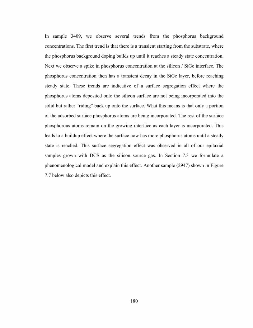
180
In sample 3409, we observe several trends from the phosphorus background
concentrations. The first trend is that there is a transient starting from the substrate, where
the phosphorus background doping builds up until it reaches a steady state concentration.
Next we observe a spike in phosphorus concentration at the silicon / SiGe interface. The
phosphorus concentration then has a transient decay in the SiGe layer, before reaching
steady state. These trends are indicative of a surface segregation effect where the
phosphorus atoms deposited onto the silicon surface are not being incorporated into the
solid but rather “riding” back up onto the surface. What this means is that only a portion
of the adsorbed surface phosphorus atoms are being incorporated. The rest of the surface
phosphorous atoms remain on the growing interface as each layer is incorporated. This
leads to a buildup effect where the surface now has more phosphorus atoms until a steady
state is reached. This surface segregation effect was observed in all of our epitaxial
samples grown with DCS as the silicon source gas. In Section 7.3 we formulate a
phenomenological model and explain this effect. Another sample (2947) shown in Figure
7.7 below also depicts this effect.
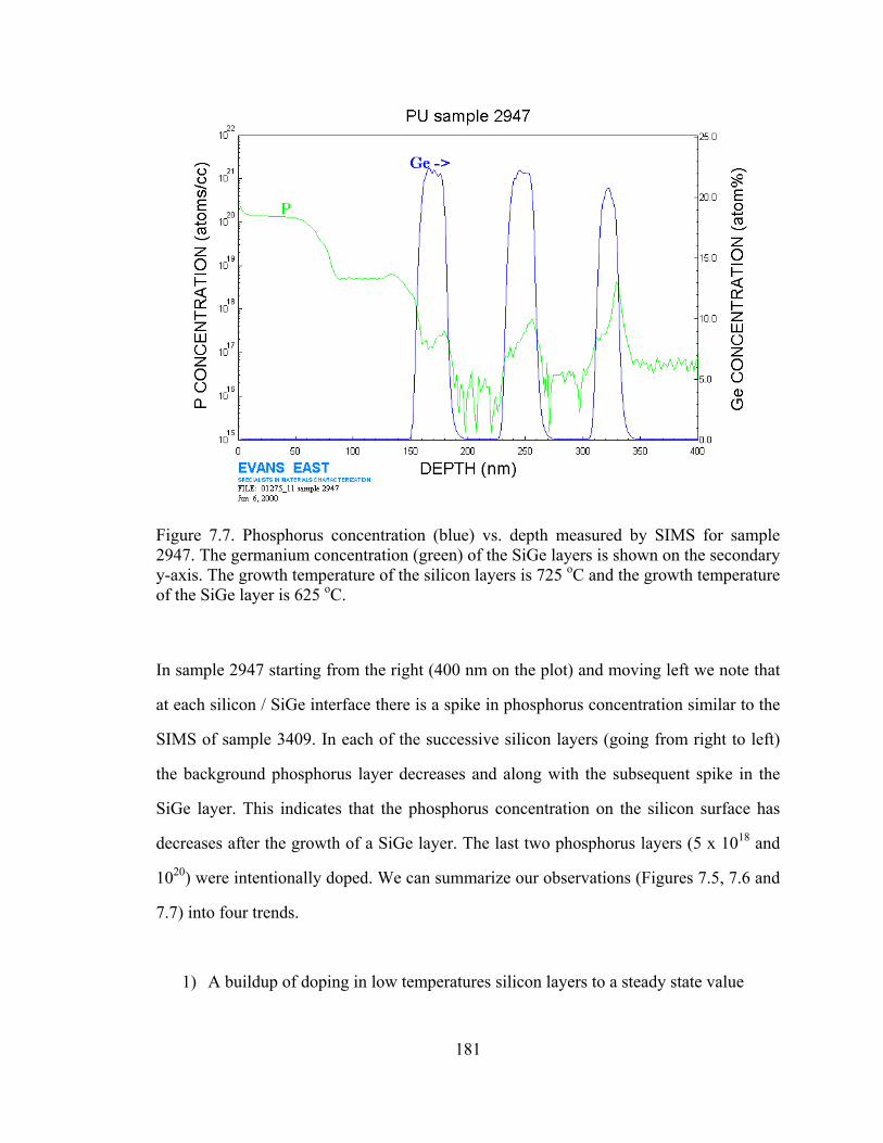
181
Figure 7.7. Phosphorus concentration (blue) vs. depth measured by SIMS for sample 2947. The germanium concentration (green) of the SiGe layers is shown on the secondary y-axis. The growth temperature of the silicon layers is 725 oC and the growth temperature of the SiGe layer is 625 oC.
In sample 2947 starting from the right (400 nm on the plot) and moving left we note that
at each silicon / SiGe interface there is a spike in phosphorus concentration similar to the
SIMS of sample 3409. In each of the successive silicon layers (going from right to left)
the background phosphorus layer decreases and along with the subsequent spike in the
SiGe layer. This indicates that the phosphorus concentration on the silicon surface has
decreases after the growth of a SiGe layer. The last two phosphorus layers (5 x 10¹⁸ and
1020) were intentionally doped. We can summarize our observations (Figures 7.5, 7.6 and
7.7) into four trends.
1) A buildup of doping in low temperatures silicon layers to a steady state value
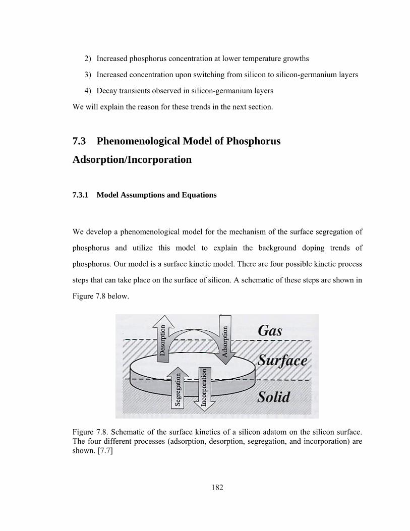
182
2) Increased phosphorus concentration at lower temperature growths
3) Increased concentration upon switching from silicon to silicon-germanium layers
4) Decay transients observed in silicon-germanium layers
We will explain the reason for these trends in the next section.
7.3 Phenomenological Model of Phosphorus
Adsorption/Incorporation
7.3.1 Model Assumptions and Equations
We develop a phenomenological model for the mechanism of the surface segregation of
phosphorus and utilize this model to explain the background doping trends of
phosphorus. Our model is a surface kinetic model. There are four possible kinetic process
steps that can take place on the surface of silicon. A schematic of these steps are shown in
Figure 7.8 below.
Figure 7.8. Schematic of the surface kinetics of a silicon adatom on the silicon surface. The four different processes (adsorption, desorption, segregation, and incorporation) are shown. [7.7]

183
The four kinetic steps are desorption from the silicon surface into the gas phase,
adsorption from the gas phase onto the silicon surface, incorporation from the surface
into the solid, and segregation from the solid back onto the surface. We can write the
change in phosphorus surface concentration with the following equation:
Eq. 7.5 ISDAdtd
−+−=θ
Where θ is the surface concentration of phosphorus, A is adsorption, D is desorption, S is
segregation from the substrate back to the surface and I is incorporation. Based on the
results in another paper, we safely assume that no desorption can occur at temperatures <
800 oC [7.8].
We will describe the adsorption as a function of temperature, material and growth
conditions (i.e. A = A(T,M) where T is the temperature and M is the material). We will
assume that no segregation (diffusion) from the substrate occurs back to the surface (S =
0). Due to the small diffusion constants at low temperatures, (i.e. 4.2*10-19cm2/s at 700 oC & 3.6*10-18 cm2/s at 750 oC [7.9]), atoms in the substrate cannot diffuse back to the
growing surface. This segregration is different then surface segregation, later described in
this chapter. We write the equation for the diffusion length below:
Eq. 7.6 2( * ) /L D t t L D= ⇒ =
where, L is the diffusion length, D is the diffusion constant and t is time. For instance, to
segregate (diffuse) through two monolayers at 700 oC, it takes 103 seconds. During that
time 190 monolayers of silicon are grown for our typical growth rates. We assume the
incorporation I, is a linear function of the surface concentration θ, and an incorporation

184
constant that is dependent on temperature, material, and growth conditions (i.e. I = θs *
i(T,M) ).
Equation 7.5 is rewritten as the following equation below:
Eq. 7.7 ),(*),( MTiMTAdtd
Sθθ
−=
We will obtain the boundary conditions from the initial concentration and the steady state
final condition to solve the non-homogenous linear differential equation. At steady state,
dθ / dt = 0, hence A(T,M) = θs * i(T,M) = I(T,M), so that the adsorption is equivalent to
the incorporation. This is expected since at steady state every adatom adsorbed is
incorporated. We know that the dopant concentration ND, is equal to the incorporation
rate ( I(T,M)) divided by the growth rate, GR. We can now express the adsorption rate as
the following equation:
Eq. 7.8 A(T,M) = θs * i(T,M) = I(T,M) = ND*GR
When not in steady state if A and i are constant, we can also express the surface
concentration as a function of time with a steady state term and a transient term.
Eq. 7.9 ),(**),(),( MTit
S eCMTiMTA −+=θ
where C is a constant determined by the boundary conditions. At steady state the surface
concentration is the adsorption divided by the incorporation (θs = A(T,M) / i(T,M)). The
dopant concentration in the growing layer is now rewritten in Equation 7.10 below:
Eq. 7.10 R
S
RD G
MTitGItN ),(*)()( θ
==

185
The instantaneous doping is determined by the surface concentration, incorporation time
constant and growth rate. There are only two fitting parameters in our model: the
adsorption rate, A(T,M) and the incorporation constant, i(T,M), both of which depend on
the temperature, T, and the material, M (silicon or Si1-xGex) and the growth conditions.
From these two parameters both the surface concentration θ and the dopant concentration
ND are fitted to the SIMS results.
7.3.2 Demonstration of Model Fitting and Results
A program was written using MATLAB for curve fitting our model with the SIMS
results. A demonstration fit was done for sample 3409 (shown in Figure 7.6) in Figure 7.9
below:
Figure 7.9. Demonstration fit of our model (orange) with the SIMS (blue) plot of phosphorus concentration vs. depth for sample 3409 (Figure 7.6).
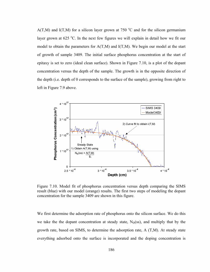
186
A(T,M) and I(T,M) for a silicon layer grown at 750 oC and for the silicon germanium
layer grown at 625 oC. In the next few figures we will explain in detail how we fit our
model to obtain the parameters for A(T,M) and I(T,M). We begin our model at the start
of growth of sample 3409. The initial surface phosphorus concentration at the start of
epitaxy is set to zero (ideal clean surface). Shown in Figure 7.10, is a plot of the dopant
concentration versus the depth of the sample. The growth is in the opposite direction of
the depth (i.e. depth of 0 corresponds to the surface of the sample), growing from right to
left in Figure 7.9 above.
Figure 7.10. Model fit of phosphorus concentration versus depth comparing the SIMS result (blue) with our model (orange) results. The first two steps of modeling the dopant concentration for the sample 3409 are shown in this figure.
We first determine the adsorption rate of phosphorus onto the silicon surface. We do this
we take the the dopant concentration at steady state, ND(ss), and multiply that by the
growth rate, based on SIMS, to determine the adsorption rate, A (T,M). At steady state
everything adsorbed onto the surface is incorporated and the doping concentration is

187
equal to the adsorbed phosphorus atoms divided by the growth rate. We then fit the curve
to obtain the incorporation rate, i (T,M). The surface concentration was also determined
using Equation 7.9 above. Now that we have determined both the adsorption and
incorporation rate we can calculate the surface concentration based on Equation 7.9. The
surface concentration versus depth is plotted in Figure 7.11 below. From Figure 7.11 we
observe that the surface concentration is slowly building up to a certain steady state value
in the range of 6-7 * 1012 / cm2. This is indicating that the phosphorus on the surface is
segregating back to the surface (i.e. riding back up to the surface instead of being
incorporated), with approximately one hundredth of a monolayer of phosphorus left on
the surface.
Figure 7.11. Plot of surface phosphorus concentration versus the depth. The surface phosphorus concentration was determined from our model.
We now demonstrate our model fit for the rest of the sample 3409 starting from the
transition from Si to SiGe and into the Si capping layer. The comparison between the
model and the SIMS result is shown below in Figure 7.12.

188
Figure 7.12. Model fit of phosphorus concentration versus depth comparing the SIMS result (blue) with our model (orange) results.
We first obtain A(T,M) from the steady state value of ND (Step 1). Then we fit the curve
of the exponential decay of the phosphorus in the SiGe layer to obtain i(T,M) (Step 2).
Note that there is a sudden discontinuous (Step 3) increase in the phosphorus
concentration (7.12) at the start of the SiGe layer. This is due to a difference in the
incorporation rate of phosphorus between silicon and SiGe (i.e. i(750oC, Si) not equal to
i(625oC, Si0.8Ge0.2). Note that the area under the curve from the peak phosphorus
concentration to the steady state concentration is equivalent to the surface concentration
at the interface at the transition from silicon to SiGe deposition. In Figure 7.13 below, we
plot the surface concentration of phosphorus starting from the transition from Si to SiGe
and into the Si capping layer.
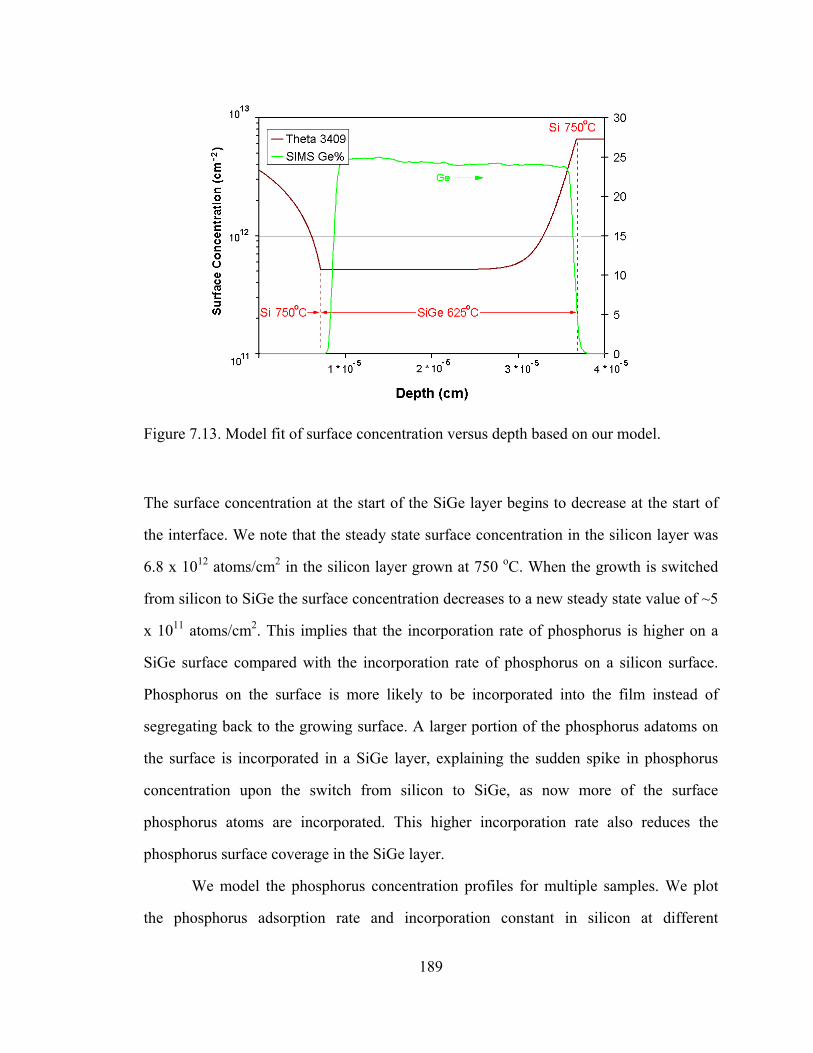
189
Figure 7.13. Model fit of surface concentration versus depth based on our model.
The surface concentration at the start of the SiGe layer begins to decrease at the start of
the interface. We note that the steady state surface concentration in the silicon layer was
6.8 x 10¹² atoms/cm2 in the silicon layer grown at 750 oC. When the growth is switched
from silicon to SiGe the surface concentration decreases to a new steady state value of ~5
x 1011 atoms/cm2. This implies that the incorporation rate of phosphorus is higher on a
SiGe surface compared with the incorporation rate of phosphorus on a silicon surface.
Phosphorus on the surface is more likely to be incorporated into the film instead of
segregating back to the growing surface. A larger portion of the phosphorus adatoms on
the surface is incorporated in a SiGe layer, explaining the sudden spike in phosphorus
concentration upon the switch from silicon to SiGe, as now more of the surface
phosphorus atoms are incorporated. This higher incorporation rate also reduces the
phosphorus surface coverage in the SiGe layer.
We model the phosphorus concentration profiles for multiple samples. We plot
the phosphorus adsorption rate and incorporation constant in silicon at different
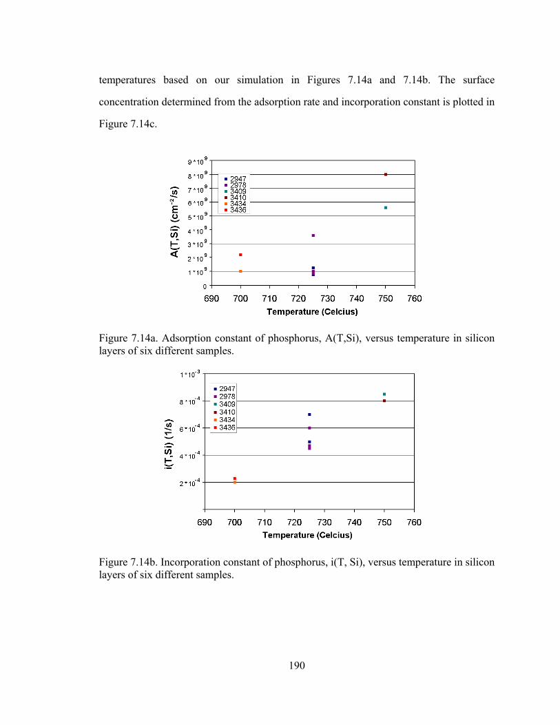
190
temperatures based on our simulation in Figures 7.14a and 7.14b. The surface
concentration determined from the adsorption rate and incorporation constant is plotted in
Figure 7.14c.
Figure 7.14a. Adsorption constant of phosphorus, A(T,Si), versus temperature in silicon layers of six different samples.
Figure 7.14b. Incorporation constant of phosphorus, i(T, Si), versus temperature in silicon layers of six different samples.

191
Figure 7.14c. Steady state surface phosphorus concentration versus temperature for silicon layers in six samples. The surface concentration was determined from our model.
From Figure 7.14a above, the data has some scatter most likely due to different
background phosphorus levels in the reactor chamber on different days. As a general
trend the adsorption rate is increasing faster than linearly with respect to temperature and
on the order of 109 atoms /cm2-sec. This may be due to more hydrogen desorption from
the surface at higher temperatures, allowing more open sites for phosphorous adsorption,
for the same phosphorus background source. There may also be increased desorption off
of the chamber walls, where phosphorus may have adsorbed onto, leading to readsorption
onto the silicon surface. In Figure 7.14b, we find that the incorporation constant is also
increasing with temperature. This has less scatter than the adsorption, A. This is expected
since it is a property of the surface, describing what fraction of the surface layer is
incorporated into the solid as the growth proceeds. We note that the surface concentration
(Figure 7.14c) has no clear trend with respect to temperature.
We plot the phosphorus adsorption rate and incorporation constant in SiGe at 625 oC for different concentrations based on our simulation in Figures 7.15a and 7.15b. The

192
surface concentration determined from the adsorption rate and incorporation constant is
plotted in Figure 7.15c.
Figure 7.15a. Adsorption constant of phosphorus, A(625oC,SiGe), versus germanium percentage of seven different samples.
Figure 7.15b. Incorporation constant of phosphorus, A(625oC,SiGe), versus germanium percentage for seven different samples. The red line indicated the maximum incorporation constant of the silicon samples in Figure 7.14b.

193
Figure 7.15c. Steady state surface phosphorus concentration versus germanium percentage for seven different samples. The surface concentration was determined from our model.
In Figure 7.15a, as we increase the germanium content in the layers, the adsorption
constant increases (but not significantly). We do not know if the jump from ~21% to 25%
is significant or just due to sample to sample variations, such as lower background
phosphorus in the reactor when the samples for ~21% Ge were grown. The adsorption
rate is on the order of 109 atoms/ cm2, on the same order as the adsorption rate resulting
from silicon films. The incorporation rate constant, i(625oC,SiGe), which determines the
amount of the surface concentration incorporated into the film, is an order of magnitude
greater than that for silicon. This is consistent with the phosphorus spikes when
transitioning from silicon to SiGe layers (see equation 7.10 above, also trend (3)). The
high incorporation rate constant indicates that there is less surface segregation of
phosphorus in the presence of germanium on the growth surface. Furthermore, we
compare the steady state phosphorus surface concentrations for the silicon and SiGe
layers (Figures 7.14c & 7.15c above) determined from our model. The steady state
surface concentrations for the silicon are roughly in the mid-1012/cm2 range (roughly one
hundredth of a monolayer). The surface concentration is the SiGe layers are on the
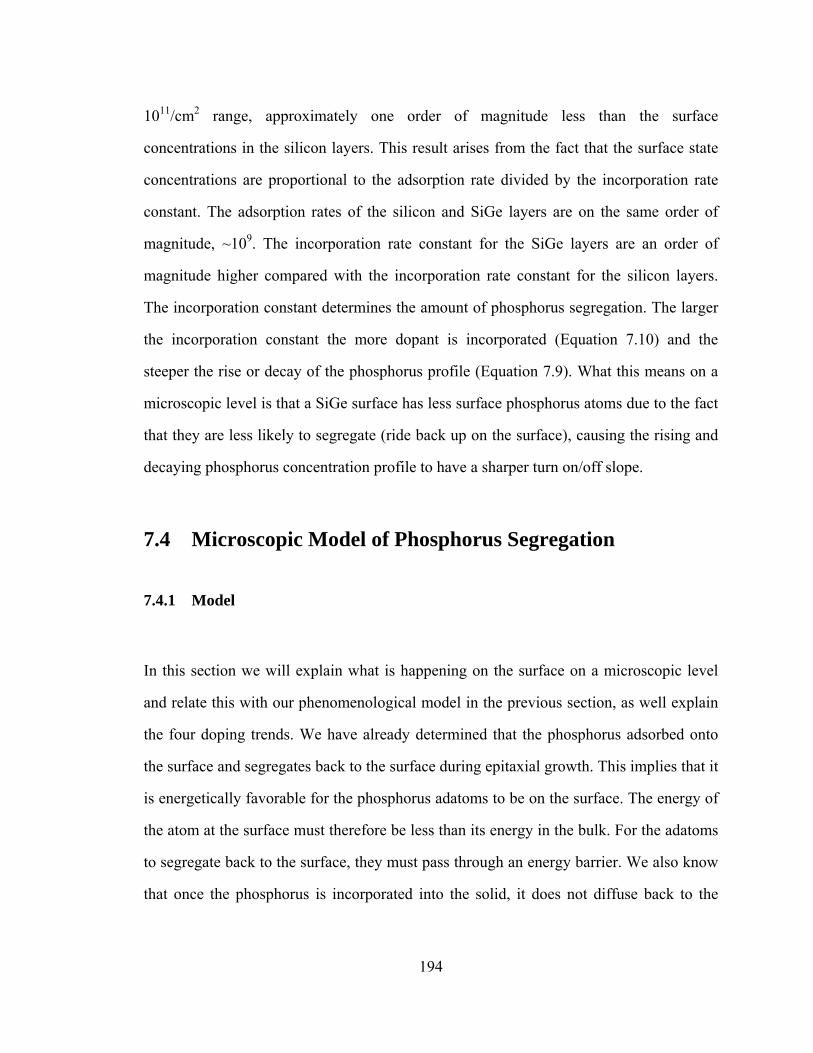
194
1011/cm2 range, approximately one order of magnitude less than the surface
concentrations in the silicon layers. This result arises from the fact that the surface state
concentrations are proportional to the adsorption rate divided by the incorporation rate
constant. The adsorption rates of the silicon and SiGe layers are on the same order of
magnitude, ~109. The incorporation rate constant for the SiGe layers are an order of
magnitude higher compared with the incorporation rate constant for the silicon layers.
The incorporation constant determines the amount of phosphorus segregation. The larger
the incorporation constant the more dopant is incorporated (Equation 7.10) and the
steeper the rise or decay of the phosphorus profile (Equation 7.9). What this means on a
microscopic level is that a SiGe surface has less surface phosphorus atoms due to the fact
that they are less likely to segregate (ride back up on the surface), causing the rising and
decaying phosphorus concentration profile to have a sharper turn on/off slope.
7.4 Microscopic Model of Phosphorus Segregation
7.4.1 Model
In this section we will explain what is happening on the surface on a microscopic level
and relate this with our phenomenological model in the previous section, as well explain
the four doping trends. We have already determined that the phosphorus adsorbed onto
the surface and segregates back to the surface during epitaxial growth. This implies that it
is energetically favorable for the phosphorus adatoms to be on the surface. The energy of
the atom at the surface must therefore be less than its energy in the bulk. For the adatoms
to segregate back to the surface, they must pass through an energy barrier. We also know
that once the phosphorus is incorporated into the solid, it does not diffuse back to the
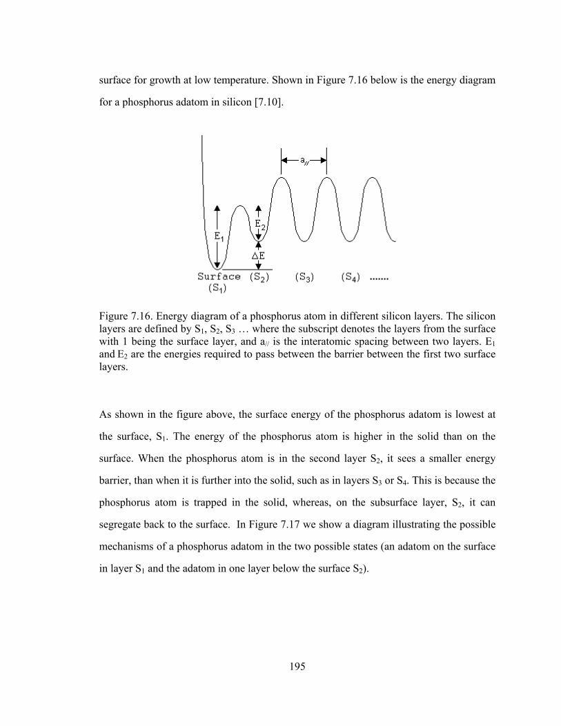
195
surface for growth at low temperature. Shown in Figure 7.16 below is the energy diagram
for a phosphorus adatom in silicon [7.10].
Figure 7.16. Energy diagram of a phosphorus atom in different silicon layers. The silicon layers are defined by S1, S2, S3 … where the subscript denotes the layers from the surface with 1 being the surface layer, and a// is the interatomic spacing between two layers. E1 and E2 are the energies required to pass between the barrier between the first two surface layers.
As shown in the figure above, the surface energy of the phosphorus adatom is lowest at
the surface, S1. The energy of the phosphorus atom is higher in the solid than on the
surface. When the phosphorus atom is in the second layer S2, it sees a smaller energy
barrier, than when it is further into the solid, such as in layers S3 or S4. This is because the
phosphorus atom is trapped in the solid, whereas, on the subsurface layer, S2, it can
segregate back to the surface. In Figure 7.17 we show a diagram illustrating the possible
mechanisms of a phosphorus adatom in the two possible states (an adatom on the surface
in layer S1 and the adatom in one layer below the surface S2).

196
Figure 7.17. Diagram showing the incorporation and segregation mechanisms from an energy perspective. θS1 and θS2 are the surface concentrations, E1 and E2 are the energy barriers, and T1 and T2 are the number of transitions going from layer 1 to layer 2 and vice versa.
θS1 and θS2 are the phosphorous concentrations in the surface layer S1 and the next layer
below the surface S2. E1 and E2 are the energy barriers for an adatom to cross from layer
S1 to S2 (E1) and the energy to cross from layer S2 to S1 (E2) respectively. T1 and T2 are
the transition rate per atom going from layer S1 to S2 and from layer S2 to S1 respectively.
In order for the phosphorus adatom to be incorporated in the solid it would have to be in
layer S2 when the new silicon monolayer is grown (Figure 7.18 dotted blue line).
Figure 7.18. Diagram showing the change in the energy barriers as a monolayer of silicon is grown onto the structure.

197
The phosphorus adatom will then be incorporated into the solid as the energy barrier
required for diffusion in between bulk layers (i.e. from S3 to S2) are much higher than the
energy barrier for diffusion from the second layer, S2, to the surface layer. If the adatom
were on the surface layer S1 when the new monolayer is grown on top of it, it would then
be in layer S2 (Figure 7.18 dotted blue line). In equilibrium, the rate of number of
phosphorus atoms going between the layers S1 and S2 is constant (i.e. r12 (rate going from
S1 to S2) = r21 (rate going from S2 to S1)). Since the rate is the surface concentration times
the number of transitions this implies that r12 = θS1 * T1 and r21 = θS2 * T2, and θS1 * T1 =
θS2 * T2. We write the transitions T1,2 as a function of the energy barrier and temperature,
T1 = C e-E1/kBT and T2 = C e-E2/kBT, where C is a constant and kB is Boltzmann’s constant.
From this we can obtain the ratio of the surface concentrations at steady state as the
following equation:
Eq. 7.11 2
2 1
1
/( )/ /1 2
/2 1
**
BB B
B
E k TE E k T E k TS
E k TS
T C e e eT C e
θθ
−− − ∆
−= = = =
From the equation above we find that the ratio of the phosphorus concentration on the
surface and the subsequent layer depends exponentially on the difference in the energies
E2 and E1, ∆E (see Figure 7.17).
We will now use this to explain why we observe the exponential rise and decay
tails of the phosphorus doping. We will consider the simple case of a constant number of
surface atoms with no further adsorption such that θT = θS1 + θS2. θT is the total of atoms
on both the top surface layer, θS1, and the subsurface layer, θS2, the only layer that can
directly segregate back to the surface layer, θS1. Let’s define a “surface factor” f as f =
exp (-∆E / kB T). We can now write θT = θS1 + f θS1 using Equation 7.11. We can now
write the surface concentrations θS1 and θS2 in terms of θT and f below in Equation 7.12.

198
Eq. 7.12 11 * ;
1S Tfθ θ=
+ 2 * ;
1S Tf
fθ θ=
+
Note that if f <<1, as it would be if the case of surface segregation, θS2/θT ~f. When the
next monolayer is grown the concentration θS2 is now trapped in. Thus we may think of f
as the fraction of the total surface layer θT incorporated into the solid during the growth
of each monolayer.
After the monolayer, the new total number of atoms in the surface and the first
layer below the surface is θT’ = θS1. The new surface concentrations are given by
equation 7.13 below. The primes indicate the new concentration on the surface and in the
next layer.
Eq. 7.13 ( )1 2
1 1' * ' * ;1 1
S T Tf fθ θ θ= =
+ +
( )2 2* ' * ;1 1
S T Tf f
f fθ θ θ= =
+ +
The ratio of the concentration of the previous layer to the new layer is 1/(1+f). This leads
to exponential decay of the phosphorus concentration. We can write the surface
concentration as the following equation:
Eq. 7.14 tLx
S eC−
= *θ
where Lt (the transition length) is define as the distance for the surface concentration to
decay by a factor of 1/e. Assume that this requires N atomic layers so LD = aSi N. Then
the ratio of the phosphorus concentration between the Nth layer (transition layer) and the
original layer is ( ) ef N
11
1=
+. We plot the concentrations of the next several layers in
Figure 7.19 below:

199
Figure 7.19. Table of surface concentrations starting with a total of θT surface phosphorous atoms and segregating the surface atoms as the next layer is grown for a total of four layers grown. The surface concentration follows an exponential decay.
As shown in Figure 7.19, surface segregation of phosphorus adatoms leads to the
exponential decay that is observed in the SiGe layers.
We now quantitatively relate our phenomenological model with our microscopic
model. From above, (1+f)N = e, so
Eq. 7.15 1ln(1 )
Nf
=+
.
200
Since T
Si
LNa
= , we have an expression which relates the decay length LT to f, which itself
depends on the energy difference of the phosphorus and the surface and the next layer
below it.
Eq. 7.16 ln(1 )
SiT
aLf
=+
The decay of the surface concentration is then (from Equation 7.14)
Eq. 7.17 ln(1 )
* *t Si
x x fL a
S C e C eθ− − +
= =
From our phenomenological model, the transient is * ( , )* t i T MS C eθ −= (Equation 7.9).
Comparing Equations 7.9 and Equation 7.17 and noting x =gr * t gives
Eq. 7.18 LT = gr / i(T,M)
Using Equations 7.16 & 7.18 to eliminate LT one has
Eq. 7.19 ln(1+f) = aSi * i(T,M) / gr
To find the surface factor f from the data, in principle one can use the data for L,
estimated directly from SIMS, to work backwards using Equation 7.16. Alternatively, f
can be found from i(T,M) using Equation 7.19.
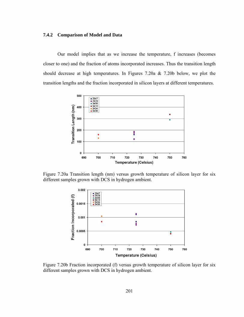
201
7.4.2 Comparison of Model and Data
Our model implies that as we increase the temperature, f increases (becomes
closer to one) and the fraction of atoms incorporated increases. Thus the transition length
should decrease at high temperatures. In Figures 7.20a & 7.20b below, we plot the
transition lengths and the fraction incorporated in silicon layers at different temperatures.
Figure 7.20a Transition length (nm) versus growth temperature of silicon layer for six different samples grown with DCS in hydrogen ambient.
Figure 7.20b Fraction incorporated (f) versus growth temperature of silicon layer for six different samples grown with DCS in hydrogen ambient.
202
From Figure 7.20a above, we note that the transition is decreasing with temperature and
the fraction of atoms incorporated increases with temperature. This is counterintuitive to
what our model suggests. This implies that the ratio of surface to subsurface adatoms is
unable to reach its equilibrium value (which was an assumption of the model). It seems
that the atoms on the subsurface are not having enough time to segregate back to the
surface. This indicates that to obtain a high concentration of phosphorus doping during
silicon growth lower temperatures and/or higher growth rates should be used to “freeze
out” the adsorbed adatoms. This implies that high-order silanes, because they allow lower
growth temperatures and/or faster growth, should allow for higher incorporation levels
for phosphorus doping. (As an aside, we would also like to note that the addition of
chlorine during growth can increase the phosphorus dopant concentration levels by
reducing the amount that is segregated back to the surface [7.12][7.13]).
7.5 Phosphorus Doping with High-Order Silanes
The growth of in-situ heavily doped (> 10 20/ cm2) phosphorus layers in silicon
can be used to make low resistance layers, as desired in source/drains. Conventionally, to
obtain these doping levels ion implantation is required. After ion implantation, the silicon
surface becomes amorphous due to the implant damage and the dopants have to be
activated (i.e. occur a substitutional lattice site). To repair all the ion implantation damage
and to activate the dopants, annealing at high temperatures (T > 900 oC) is required.
Annealing at high temperatures however, causes the diffusion of phosphorous atoms,
which prevents the formation of abrupt junctions and can change device profiles. In this
section of the chapter we explore the use of high-order silanes for the growth of heavily
doped phosphorus layers.

203
As described in previous sections of this chapter, the surface segregation of
phosphorous makes it difficult to obtain high phosphorus doping concentrations.
Furthermore, it has been shown that a high level of phosphorus doping can inhibit the
growth of silicon by “poisoning” the surface (i.e. removing possible open sites for
adsorption), thereby reducing the growth rate [7.13]. This occurs when a high phosphorus
concentration builds up on the silicon surface and forms stable dimer pairs, which inhibit
silicon adsorption.
We have previously shown (Chapter 4) that the growth with high-order silanes
may not require open surface sites. A surface with a high level of phosphorus might not
inhibit the growth rate when high-order silanes are used. High-order silanes also have
high growth rates at low temperatures. We conducted experiments using phosphine to
determine it there is any reduction of growth rate caused by phosphorus during epitaxial
growth with disilane and NPS, as is observed with silane and DCS growth. Samples were
grown with a chamber pressure of 6 torr and 3 slpm hydrogen flow with varying
phosphine gas flows, silicon precursor gas flows and growth temperature. A plot of the
normalized growth rate versus phosphorus flow (sccm) is shown in Figure 7.21 below.
Figure 7.21. Normalized growth rate versus phosphine flow rate for four different silicon precursors at different growth temperatures. The growth rates (measured by SIMS) were normalized by the growth rate without any intentional phosphine doping.
204
As the phosphine flow is increased, the normalized growth rate decreases when the
silicon source was silane or DCS. Ideally, the growth rates used in the experiments would
be similar for different silicon precursors. However, due to experimental limitations
(MFC flow controllers limiting the amount of gas we could flow) and the large
discrepancy between the growth rates of the different precursors, the growth rates of the
samples varied about one order magnitude for the samples. The growth rates without
phosphine flow were 12.5 nm/min and 1.2 nm/min for silane at 700oC and 625oC; 19.5
nm/min and 3.7 nm/min for disilane at 625 oC and 575 oC; 23 nm/min and 4.8 nm/min for
NPS at 625 oC and 575 oC; and 40 nm/min and 3 nm/min for DCS at 800 oC and 700oC
respectively.
The decrease in the normalized growth rate is much smaller when disilane was the
silicon source and was not observed when NPS was the silicon source. This may be due
to the fact that the growth mechanism with high-order silanes is concerted reactions that
do not depend on the open site fraction, unlike conventional gases such as DCS and
silane. This may also imply a smaller phosphorus concentration on the growth surface
with disilane and NPS.
We will now compare the total phosphorus concentration versus the phosphine
flow rate in Figure 7.22 below, to determine if higher phosphorus concentrations can be
achieved with high-order silanes.
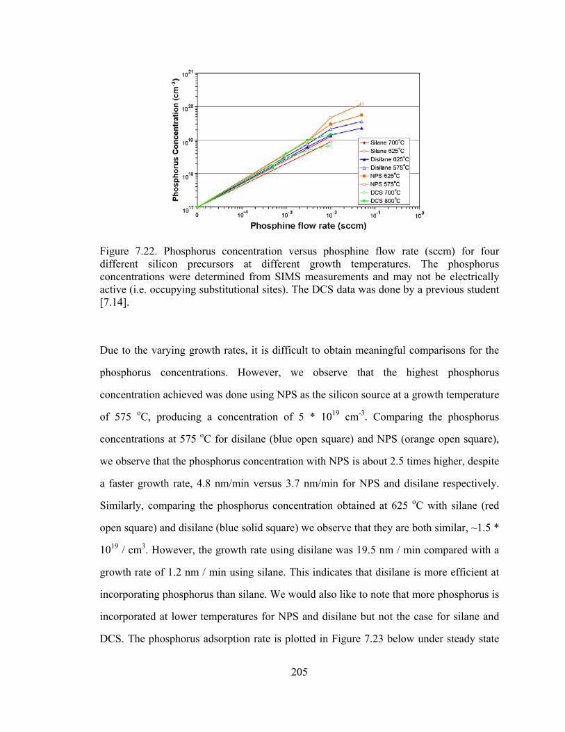
205
Figure 7.22. Phosphorus concentration versus phosphine flow rate (sccm) for four different silicon precursors at different growth temperatures. The phosphorus concentrations were determined from SIMS measurements and may not be electrically active (i.e. occupying substitutional sites). The DCS data was done by a previous student [7.14].
Due to the varying growth rates, it is difficult to obtain meaningful comparisons for the
phosphorus concentrations. However, we observe that the highest phosphorus
concentration achieved was done using NPS as the silicon source at a growth temperature
of 575 oC, producing a concentration of 5 * 1019 cm-3. Comparing the phosphorus
concentrations at 575 oC for disilane (blue open square) and NPS (orange open square),
we observe that the phosphorus concentration with NPS is about 2.5 times higher, despite
a faster growth rate, 4.8 nm/min versus 3.7 nm/min for NPS and disilane respectively.
Similarly, comparing the phosphorus concentration obtained at 625 oC with silane (red
open square) and disilane (blue solid square) we observe that they are both similar, ~1.5 *
1019 / cm3. However, the growth rate using disilane was 19.5 nm / min compared with a
growth rate of 1.2 nm / min using silane. This indicates that disilane is more efficient at
incorporating phosphorus than silane. We would also like to note that more phosphorus is
incorporated at lower temperatures for NPS and disilane but not the case for silane and
DCS. The phosphorus adsorption rate is plotted in Figure 7.23 below under steady state

206
conditions with every adsorbing phosphorus atom being incorporated, shown previously
in chapter 4 (Figure 4.26).
Figure 7.23. Normalized adsorption rate w.r.t. phosphine pressure vs. epitaxy temperature for the silicon sources of silane, disilane and NPS.
When we compare the phosphine adsorption rate for the three precursors at the same
temperature, we observe that the phosphine adsorption rate increases with increasing
silane order. Similar to boron, phosphine adsorption depends directly on the number of
open sites. The increasing phosphorus adsorption rate indicates that the number of open
sites for phosphorus adsorption is higher with high-order silanes, providing further
evidence to the creation of open sites during epitaxial growth using high-order silanes.
We compare the growth rate vs. the phosphorus concentration in the silicon layers
grown with different silicon precursors at different temperatures. The growth was done
with a chamber pressure of 6 torr, with 3 slpm hydrogen flow and 0.01 sccm of
phosphine flow (partial pressure = 2 x 10⁻⁵ torr). The results are plotted in Figure 7.24
below:
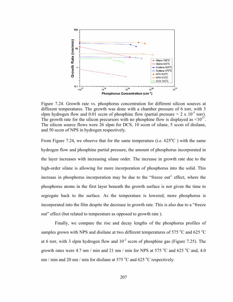
207
Figure 7.24. Growth rate vs. phosphorus concentration for different silicon sources at different temperatures. The growth was done with a chamber pressure of 6 torr, with 3 slpm hydrogen flow and 0.01 sccm of phosphine flow (partial pressure = 2 x 10⁻⁵ torr). The growth rate for the silicon precursors with no phosphine flow is displayed as <1017. The silicon source flows were 26 slpm for DCS, 10 sccm of silane, 5 sccm of disilane, and 50 sccm of NPS in hydrogen respectively.
From Figure 7.24, we observe that for the same temperature (i.e. 625oC ) with the same
hydrogen flow and phosphine partial pressure, the amount of phosphorus incorporated in
the layer increases with increasing silane order. The increase in growth rate due to the
high-order silane is allowing for more incorporation of phosphorus into the solid. This
increase in phosphorus incorporation may be due to the “freeze out” effect, where the
phosphorus atoms in the first layer beneath the growth surface is not given the time to
segregate back to the surface. As the temperature is lowered, more phosphorus is
incorporated into the film despite the decrease in growth rate. This is also due to a “freeze
out” effect (but related to temperature as opposed to growth rate ).
Finally, we compare the rise and decay lengths of the phosphorus profiles of
samples grown with NPS and disilane at two different temperatures of 575 oC and 625 oC
at 6 torr, with 3 slpm hydrogen flow and 10-2 sccm of phosphine gas (Figure 7.25). The
growth rates were 4.7 nm / min and 21 nm / min for NPS at 575 oC and 625 oC and, 4.0
nm / min and 20 nm / min for disilane at 575 oC and 625 oC respectively.
208
Figure 7.25. Rise and decay slopes as measured by SIMS for NPS and disilane at 575 oC and 625 oC respectively. The slopes were measured from samples 4850 (DS) and 4866 (NPS) (see Appendix E).
The smaller rise and decay slope of NPS when compared to disilane implies that NPS has
a higher incorporation constant. Furthermore, both the rise and decay slope are smaller at
lower temperatures for both gases, indicating that the phosphorus atoms on the surface
are “freezing out” and do not have enough time to segregate at reduced temperatures. We
do not know the reason why the slopes are reduced when NPS is used or why the rise and
decay slopes are not the same.
209
7.6 Summary
In this chapter we have discussed the unwanted background concentration of phosphorus
due to growth with DCS with SIMS and C-V measurements on Schottky diodes. A
phenomenological model was made to model and to explain the phosphorus segregation
trends that are commonly observed in from silicon and SiGe samples grown with our
CVD system. Our phenomenological model was then compared with a microscopic
model of how individual phosphorus adatoms are incorporated. Experimentally we found
that low temperatures and high-growth rates can reduce surface segregation and hence
increase phosphorus incorporation. This implies that high-order silanes should be used
for growth of heavily phosphorus doped layers. Phosphorus doping experiments were
conducted with different silicon precursors. We observed that high-order silanes are more
efficient at incorporating phosphorous into the grown layers. This may be due to a freeze
out effect, where the higher growth rate is preventing the surface segregation of
phosphorus back to the surface.

210
Chapter 8
Summary and Conclusion
In this work, we have qualified the use of NPS as a silicon source in chemical
vapor deposition. Characterization techniques such as (secondary ion mass spectrometry
(SIMS), photoluminescence (PL), UV reflectance, and cross-sectional TEM) were
conducted on epitaxial layers grown with NPS are analyzed and indicated that good
quality epitaxial silicon layers can be grown with NPS. All deposition with NPS on oxide
was found to be amorphous silicon. Etch rates of amorphous silicon layers are much
higher than etch rates of crystalline silicon, implying that NPS is a suitable candidate for
selective silicon deposition via a CDE (Cyclical Deposition and Etch) process. Field
effect transistors (FETs) were fabricated in epitaxial layers grown with NPS. Based on
carrier mobilities and curve-tracer plots we concluded that the quality of the epitaxial
layers grown with NPS are comparable to the quality of epitaxial layers of prime grade
silicon substrates.
The basic CVD silicon growth theory on a macroscopic, microscopic, and
atomistic level was covered in this thesis. The conventional hydrogen desorption model
of silicon growth was found to be inadequate in explaining high growth rates and low
temperatures. Silicon growth with high-order silanes were significantly less dependent on
conventional hydrogen desorption and qualitatively determined to generate its own open
sites. A novel concerted reaction mechanism without the need for hydrogen desorption
was proposed as the reason for the enhancement of growth rates with high-order silanes.
This mechanism was supported by our experimental data using disilane and
neopentasilane and by data from other groups using higher-order silanes such as trisilane.
Smoother surfaces were also found with deposition from high-order silanes compared

211
with conventional silane under similar conditions, and can be explained by our novel
model.
The ability of high-order silanes to deposit and low-temperatures and high-growth
rates, makes them an attractive candidate for the epitaxial growth of dilute random carbon
alloys of silicon (Si:C) and for heavily-doped-phosphorus layers in silicon. Higher
substitutional carbon and phosphorus levels are achieved with NPS compared to silane
and disilane under similar experimental conditions.
Figure 8.1 Synopsis of the effects of increasing the silane order. As the silane order is increased the growth rate increases and the smoothness of the deposited films improves.

212
List of References Chapter 1 References
[1.1] H. C. Theuerer, “Epitaxial Silicon Films by the Hydrogen Reduction of SiCl4,”
Journal of the Electrochemical Society, v108, pp. 649-653 (1961)
[1.2] B. D. Joyce and J. A. Baldrey, “Selective Epitaxial Deposition of Silicon,”
Nature, v195, pp. 485-486 (1962)
[1.3] J. J. Lander and J. Morrison, “Low Voltage Electron Diffraction Study of the
Oxidation and Reduction of Silicon,” Journal of Applied Physics, v33, pp. 2089-
2092 (1962)
[1.4] R. H. Finch, H. J. Queisser, G. Thomas, and J. Washburn, “Structure and Origin
of Stacking Faults in Epitaxial Silicon,” Journal of Applied Physics, v34, pp. 406-
415 (1963)
[1.5] B. S. Meyerson, “Low-temperature Silicon Epitaxy by Ultrahigh Vacuum /
Chemical Vapor Deposition”, Applied Physics Letters, v48, pp. 797-799 (1986)
[1.6] P. V. Schwartz and J. C. Sturm, “Oxygen Incorporation During Low Temperature
Chemical Vapor Deposition Growth of Epitaxial Silicon Films,” Journal of the
Electrochemical Society, v141, pp. 1284-1290 (1994)
[1.7] T. O. Sedgwick, M. Berkenblit, and T. S. Kuan, “Low-Temperature Selective
Epitaxial Growth of Silicon at Atmospheric Pressure,” Applied Physics Letters,
v54, pp. 2689-2691 (1989)
[1.8] R. People and J. C. Bean “Calculation of Critical Thickness versus Lattice
Mismatch for GexSi1-x / Si Strained Heterostructures,” Applied Physics Letters,
v47, pp. 322-324 (August 1985)
[1.9] “Properties of Silicon Germanium and SiGe: Carbon” Edited by E. Kasper and K.
Lyutovich, pp. 22 (2000)

213
[1.10] M. Yang, M. S. Carroll, J.C. Sturm, and T. Büyüklimanli, “Phosphorus Doping
and Sharp Profiles in Silicon and Silicon-Germanium Epitaxy by Rapid Thermal
Chemical Vapor Deposition,” Journal of the Electrochemical Society, v147, pp.
3541-3545 (2000)
[1.11] T. O. Mitchell, J. L. Hoyt, and J. F. Gibbons, “Substitutional Carbon
Incorporation in Epitaxial Si1-yCy Layers Grown by Chemical Vapor Deposition,”
Applied Physics. Letters, v71, pp. 1688-1690 (1997)
Chapter 2 References
[2.1] J. C. Sturm, P. V. Schwartz, and P. M. Garone, “Silicon Temperature
Measurement by Infrared Transmission for Rapid Thermal Processing
Applications,” Applied Physcis Letters, v56, pp. 961-964 (1990)
[2.2] J. C. Sturm, P. M. Garone, and P. V. Schwartz, “Temperature Control of Silicon-
Germanium Epitaxial Growth on Silicon Substrates by Infrared Transmission,”
Journal of Applied Physics, v69, pp. 542-544 (1991)
[2.3] J.C. Sturm and C. M. Reaves. “Silicon Temperature Measurement by Infrared
Absorption Fundamental Processes and Doping Effects,” IEEE Trans. Electron
Dev., v39, pp. 81-88 (1992)
[2.4] I. Vasiliev, S. Öğüt, and J. R. Chelikowsky, “Ab Initio Absorption Spectra and
Optical Gaps in Nanocrystalline Silicon,” Physical Review Letters, v86, pp. 813-
816 (Feb 2001)
[2.5] Dow Chemical Phase Report
[2.6] G. Pares, J. L. Regolini, J. Mercier, D. Dutartre, and D. Bensahel, “Kinetic
Aspects of Epitaxial Silicon Growth using Disilane in a Rapid Thermal
Processing System,” Journal of Applied Physics, v68, n9, pp. 4885-7 (Nov 1990)
214
[2.7] Y. Suda, D. Lubben, T. Motooka, and J. E. Green, “Adsorption and Thermal
Dissociation of Disilane (Si2H6) on Si(100) 2x1,” Journal of Vacuum Science and
Technology A, v8, pp. 61-67 (1990)
[2.8] M. A. Todd and K. D. Weeks, “Low Temperature, High Growth Rate Epitaxial
Silicon and Silicon Germanium Alloy Films,” Applied Surface Science, v224 pp.
41-45 (2004)
[2.9] P. R. Fischer, M. Bauer, S. R. A. Van Averde, T. G. M. Oosterlaken, M. Yan, W.
A. Verweij, B. W. M. Bozon, and P. M. Zagwijn, “Low Temperature Silcore ®
Deposition of Undoped and Doped Silicon Films,” ECS Transactions, v3, pp.
203-215 (2006)
[2.10] M. S. Carroll, J. C. Sturm, and M. Yang, “Low-Temperature Preparation of
Oxygen- and Carbon-Free Silicon and Silicon Germanium Surfaces for Silicion
and Silicon-Germanium Epatxial Growth by Rapid Thermal Chemical Vapor
Deposition,” Journal of the Electrochemical Society, v147, pp. 4652-4659 (2000)
[2.11] M. Hierlemann, A. Kersh, C. Werner, and H. Schäfer, “A Gas-Phase and Surface
Kinetics Model for Silicon Epitaxial Growth with SiH2Cl2 in an RTCVD
Reactor,” Journal of the Electrochemical Society, v142, pp. 259-265 (1995)
[2.12] D. W. Foster, A. J. Learn, and T. I. Kamins, “Deposition Properties of Silicon
Films Formed from Silane in a Vertical-Flow Reactor,” Journal of Vacuum
Science and Technology B, v4, pp. 1182-1186 (1986)
[2.13] A. Yin and S. J. Fonash, “Oxygen-Plasma-Enhanced Crystallization of a-Si:H
Films on Glass,” Journal of Vacuum Science and Technology A, v12, pp. 1237-
1240 (1994)
[2.14] G. Harbeke, L. Krausbauer, E. F. Steigmeier, and A. E. Widmer, “Growth and
Physical Properties of LPCVD Polycrystalline Silicon Films,” Journal of the
Electrochemical Society, v131, pp. 675-682 (1984)

215
[2.15] T. I. Kamins, “Structure and Properties of LPCVD Silicon Films,” Journal of the
Electrochemical Society, v127, pp. 686-690 (1980)
[2.16] A. A. Onischuk and V. N. Panfilov, “Mechanism of Thermal Decomposition of
Silanes,” Russian Chemical Review, v70, n4, pp. 321-332 (2001)
Chapter 3 References
[3.1] D. J. Eaglesham, H.-J. Grossmann, and M. Cerullo, “Limiting Thickness hepi for
Epitaxial Growth and Room-Temperature Si Growth on Si (100),” Physical
Review Letters, v65, n10, pp. 1227-1230 (1990)
[3.2] H.-J. Grossmann, and L. C. Feldman, “Molecular Beam Epitaxy and
Reconstructed Surfaces: Initial Stages of Interface Formation in Group IV-IV
Structures,” Applied Physics A, v38, n3, pp. 171-179 (1985)
[3.3] H. Jorke, H.-J. Herzog, and H. Kibbel, “Kinetics of Ordered Growth of Si on Si
(100) at Low Temperatures,” Physics Review B, v40, pp. 2005-2008 (1989)
[3.4] F. Jona, “Study of the Early Stages of the Epitaxy of Silicon on Silicon,” Applied
Physics Letters, v9, n6, pp. 235-237 (1966)
[3.5] K. Winer, “Theory of Infrared Absorption in Silicon,” Physical Review B, v35,
n15, pp. 8189-95 (May 1987)
[3.6] J. Weber and M. I. Alonso, “Near-Band-Gap Photoluminescence of Si-Ge
Alloys”, Physical Review B, v40, n8, pp. 5683-5693 (Sept. 1998)
[3.7] P. J. Dean, J. R. Haynes, and W. F. Flood, “New Radiative Recombination
Processes Involving Neutral Donors and Acceptors in Silicon and Germanium”,
Physical Review, v161, n3, pp. 711-729 (Sept 1967)
[3.8] B. S. Meyerson, F. J. Himpsel, and K. J. Uram, “Bistable conditions for low-
temperature silicon epitaxy,” Applied Physics Letters, v57, pp. 1034-1036 (1990)
216
[3.9] M. S. Carroll, J. C. Sturm, and M. Yang, “Low-Temperature Preparation of
Oxygen- and Carbon- Free Silicon and Silicon- Germanium Surfaces for Silicon
and Silicon-Germanium Epitaxial Growth by Rapid Thermal Chemical Vapor
Deposition,” Journal of the Electrochemical Society, v147, pp. 4652-4659 (2000)
[3.10] S. M. Celik, and M. C. Öztürk, “Low Thermal Budget In Situ Surface Cleaning
for Selective Silicon Epitaxy,” Journal of the Electrochemical Society, v145, pp.
3602-3608 (1998)
[3.11] R. Oberhuber, G. Zandler, and P. Vogl, “Subband structure and mobility of two-
dimensional holes in strained Si/SiGe MOSFET’s”, Physics Review B, v58, no
15, pp. 9941-9948 (1998-9)
Chapter 4 References
[4.1a] T. Kamins, Polycrystalline Silicon for Integrated Circuits and Displays, Kluwer
Academic Publishers, 2nd
Edition, pg 8
[4.1b] L. I. Stiel and G. Thodos, “Viscosity of Hydrogen in the Gaseous and Liquid
States for Temperatures up to 5000oK”, Industrial Engineering Chemical
Fundamentals, v2, n3, pp. 233–237 (1963)
[4.1c] Chemical Rubber Company (CRC). 1984. CRC Handbook of Chemistry and
Physics. Weast, Robert C., Editor. 65th edition. CRC Press, Inc. Boca Raton,
Florida. USA.
[4.2] D. J. Chadi, “Atomic and Electronic Structures of Reconstructed Si(100)
Surfaces” Physical Review Letters, v43, n1, pp. 43-47 (1979)
[4.3] J. A. Appelbaum, G. A. Baraff, D. R. Hamann, H. D. Hagstrum and T. Sakurai,
“Hydrogen Chemisorption on the 100 (2 x 1) Surfaces of Si and Ge” Surface
Science, v70, pp. 654-673 (1978)

217
[4.4] S. Ciracri and I. P. Batra, “Theory of Transition from the Dihydride to
Monohydride Phase on the Si(001) Surface” Surface Science, v178, pp. 80-89
(1986)
[4.5] S. Ciracri, R. Butz, E. M. Oellig, and H. Wagner, “Chemisorption of hydrogen on
the Si(100) Surface: Monohydride and Dihydride Phases” Physical Review B,
v30, n2, pp. 711-720 (1984)
[4.6] M. Kitabatake, P. Fons, and J. E. Greene, “Molecular Dynamics Simulations of
Low-Energy Particle Bombardment Effects During Vapor Phase Crystal Growth:
10 eV Si Atoma Incident on Si(001) 2x1 Surface,” Journal of Vacuum Science
and Technology A, v8, pp. 3726-3735 (1990)
[4.7] K. Sinniah, M. G. Sherman, L. B. Lewis, W. H. Weinberg, J. T. Yates, Jr. and K.
C. Janda, “New Mechanism for Hydrogen Desorption from Covalent Surfaces:
The Monohydride Phase on Si (100),” Physical Review Letters, v62, n5, pp. 567-
570 (Jan 1989)
[4.8] M. C. Flowers, N. B. H. Jonathan, Y. Liu, and A. Morris, “Temperature
Programmed Desorption of Molecular Hydrogen from a Si(100)-2x1 Surface:
Theory and Experiment,” Journal of Chemical Physics, v99, n9, pp. 7038-7048
(July 1993)
[4.9] P. V. Schwartz and J. C. Sturm, “Oxygen Incorporation During Low Temperature
Chemical Vapor Deposition Growth of Epitaxial Silicon Films,” Journal of the
Electrochemical Society, v141, n5, pp. 1284-1290 (May 1994)
[4.10] J. B. Benziger, Metal-Surface Reaction Energies, VCH Publishers, New York
(1991)
[4.11] M. L. Hitchman, J. Kane, and A. E. Widmer, “Polysilicon Growth Kinetics in a
Low Pressure Chemical Vapour Deposition Reactor,” Thin Solid Films, v59, pp.
231-247 (1979)

218
[4.12] S. M. Gates, C. M. Greenlief, and D. B. Beach, “Decomposition Mechanisms of
SiHx species on Si(100)-(2x1) for x = 2, 3, and 4,” Journal of Chemical Physics,
v93, n10, pp. 7493-7503 (Nov 1990)
[4.13] I. Alkorta and J. Elguero, “Theorectical study of the bond energy in n-silanes and
n-germanes: Comparison with n-alkanes”, Chemical Physics Letters, v429, pp.
58-61 (2006)
[4.14] S.M. Gates and S.K. Kulkarni, “Kinetics of Surface Reactions of Very Low-
Pressure Chemical Vapor Deposition of Si from SiH4,” Applied Physics Letters,
v58, n25, pp. 2964-2966 (1991)
[4.15] S. M. Gates, “Adsorption Kinetics of SiH4, Si2H6, and Si3H8 on the Si(111)-(7x7)
Surface,” Surface Science v195, pp. 307-329 (1988)
[4.16] Y. Suda, D. Lubben, T. Motooka, and J. E. Greene, “Adsorption and thermal
dissociation of disilane (Si2H6) on Si (100) 2x1,” Journal of Vacuum Science and
Technology A, v8, n1, pp. 61-67 (1990)
[4.17] D.Lubben, R. Tsu, T. R. Bramlett, and J. E. Greene, “Mechanisms and kinetics of
Si atomic-layer epitaxy on Si(001)2x1 from Si2H6,” Journal of Vacuum. Science
and Technology A, v9, n6, pp. 3003-3011 (1991)
[4.18] R.Imbihl, J. E. Demuth, S. M. Gates, and B. A. Scott, “Interaction of Si2H6 with a
Si (111) – 7x7 surface,” Physical Review B, v39, pp. 5222-5233 (March 1989)
[4.19] W. A. P. Claassen and J. Bloem, “The Growth of Silicon from Silane in Cold
Wall CVD Systems,” Phillips Journal of Research, v36, pp. 123-137 (1981)
[4.20] K. H. Chung, N. Yao, J. Benziger, J. C. Sturm, K. K. Singh, D. Carlson, and S.
Kuppurao, “Ultrahigh Growth Rate of Epitaxial Silicon by Chemical Vapor
Deposition at low Temperature with Neopentasilane,” Applied Physics Letters,
v92, pp. 113506-8 (March 2008)
[4.21] T. F. Narbeshuber, H. Vinek and J. A. Lercher, “Monomolecular Conversion of

219
Light Alkanes over H-ZSM-5,” J. Catalysis, v157, pp. 388-395 (1995)
[4.22] Y.V. Kissin, Catalysis Reviews 43, pp. 85-146 (2001)
[4.23] A. Farkas and K. Bonhoeffer, Z. Phys. Chem, 231, pp. 638-640 (1931)
[4.24] S. D. Jackson, G. J. Kelly, and G. Webb, “Supported Metal Catalyst; Preparation,
Characterization, and Function: Part VI. Hydrogenolysis of Ethane, Propane, n-
Butane and iso-Butane over Supported Platinum Catalysts”, Journal of Catalysis,
v176, pp. 225-234 (1998)
[4.25] B. A. Ferguson, C. T. Reeves, D. J. Safarik, and C. B. Mullins, “Silicon
Deposition from Disilane on Si(100)-2x1: Microscopic Model Including
Adsorption,” Journal of Applied Physics, v90, pp. 4981-4989 (2001)
[4.26] P. M. Agrawal, D. L. Thompson, and L. M. Raff, “Unimolecular Dissociation
Dynamics of Disilane,” Journal of Chemical Physics, v98, pp. 1069-1082 (1990)
[4.27] S. K. Kulkarni, S. M. Gates, C. M. Greenlief, and H. H. Sawin, “Mechanisms of
Disilane Decomposition on Si(111)-7x7,” Suface Science, v239, pp. 26-35 (1990)
[4.28] W. K. Burton, N. Cabrera, and F. C. Frank, “The Growth of Crystals and the
Equilibrium Structures of Their Surfaces,” Philosophical Transactions of the
Royal Society of London, Series A. Mathematical and Physical Sciences, v243,
pp. 299-358 (Nov. 1951)
[4.29] Z. Zhang, F. Wu, and M. G. Lagally, “An Atomistic View of Si(001)
Homoepitaxy,” Annual Reviews Materials Science, v27, pp 525-553 (1997)
[4.30] D. J. Chadi, “Stabilities of Single-Layer and Bi-Layer Steps on Si(001) Surfaces,”
Physics Review Letters, v59, pp. 1691-1694 (1987)
[4.31] G. Brocks, P. J. Kelly, and R. Car, “Binding and Diffusion Energy of Si adatom
on the Si(100) surface,” Physics Review Letters, v66, pp. 1729 (1991)
[4.32] Y. W. Mo and M. G. Lagally, “Anisotropy in Surface Migration of Si and GE on
Si(001),” Surface Science, v248, pp. 313-320 (1991)

220
[4.33] B. Lewis and D. S. Campbell, “Nucleation and Initial-Growth Behavior of Thin-
Film Deposits,” Journal of Vacuum Science and Technology, v4, pp. 209-218
(1967)
[4.34] C. Pearson, M. Krueger, and E. Ganz, “Direct Tests of Microscopic Growth
Models using Hot Scanning Tunneling Microscopy Movies,” Physics Review
Letters, v76, pp. 2306-2309 (1996)
[4.35] C Roland and G. H. Gilmer, “Epitaxy on Surfaces Vicinal to Si(001). I . Diffusion
of Silicon Adatoms over Terraces,” Physical Review B, v46, pp. 13428-13436
(1992)
[4.36] M. G. Lagally, Kinetics of Ordering and Growth at Surfaces, (Plenum, New
York, 1989)
[4.37] S. H. Wolff, S. Wagner, J. C. Bean, R. Hull, and J. M. Gibson, “Hydrogen
Surface Coverage: Raising the Silicon Epitaxial Growth Temperature”, Applied
Physics Letters, v55, pp. 2017-2019 (1989)
[4.38] I. Mizushima, M. Koike, T. Sato, K. Miyano, and Y. Tsunashima, “Mechanism of
Defect Formation During Low-Temperature Si Epitaxy on Clean Si Substrate”,
Japanese Journal of Applied Physics, v38, pp. 2415-2418 (1999)
[4.39] P. Meunier-Beillard, M. Caymax, K. Van Nieuwenhuysen, G. Doumen, B. Brijs,
M. Hopstaken, L. Geenen, W. Vandervorst, “N2 as Carrier Gas: An Alternative to
H2 for the Enhanced Epitaxy of Si, SiGe and SiGe:C”, Applied Surface Science,
v224, pp. 31-35 (2004)
[4.40] D.P. Adams and S. M. Yalisove, D. J. Eaglesham, “Effect of Hydrogen on
Surface Roughening During Si Homoepitaxial Growth,” Applied Physics Letters,
v63, n26, pp. 3571-3573 (1993)

221
[4.41] J. W. Sharp and G. Eres, “Kinetics of Hydrogen Desorption From Si(100) and
Si(111) Surfaces Following Chemisorption of Disilane and Trisilane,” Surface
Science, v320, pp. 169-173 (1994)
[4.42] M.P. D’Evelyn, Y. L. Yang, and L. F. Sutcu, “π-Bonded Dimers, Preferential
Pairing, and First-Order Desorption Kinetics of Hydrogen on Si(100)-(2x1),”,
Journal of Chemical Physics, v96, n1, pp. 852-855 (1996)
[4.43] M. L. Wise, B. G. Koehler, P. Gupta, P. A. Coon, and S. M. George,
“Comparison of Hydrogen Desorption Kinetics from Si(111) 7 x 7 and Si(100) 2
x 1,” Surface Science, v258, pp. 166-176 (1991)
[4.44] U. Höfer, L. Li, T. F. Heinz, “Desorption of Hydrogen from Si(100) 2 x 1 at Low
Coverages: The Influence of π-Bonded Dimers on the Kinetics,” Physical Review
B, v45, n16, pp. 9485-9488 (1992)
[4.45] ASM Patent, WO 02/080244 (10/10/2002)
[4.46] M. Bauer, V. Machkaoutsan, and C. Arena, “Highly Tensile Strained Silicon-
Carbon Alloys Epitaxially Grown into Recessed Source Drain Areas of NMOS
Devices,” Semiconductor Science and Technology, v22, pp. S183-187 (2007)
[4.47] S. Takeuchi, N. D. Nguyen, J. Goosens, M. Caymax, R. Loo, “Si1-xGex Growth
Using Si3H8 by Low Temperature Chemical Vapor Deposition,” Thin Solid Films,
(Oct 2009), in press.
[4.48] S. K. Kulkarni, S. M Gates, C. M. Greenlief, and H. H. Sawin, “Mechanisms of
Disilane Decomposition on Si(111)-7x7,” Surface Science, v239, pp. 26-35
(1990)
Chapter 5 References
[5.1] K. W. Ang, K. J. Chui, V. Bliznetsov, C. H. Tung, A Du, N. Balasubramanian, G.
Samudra, M. F. Li, and Y. C. Yeo, “Lattice Strain Analysis of Transistor

222
Structures with Silicon-Germanium and Silicon-Carbon Source / Drain Stressor,”
Applied Physics Letters, v86, pp. 093102-1- 093102-3 (2005)
[5.2] Y. C. Yeo, “Enhancing CMOS Transistor Performance using Lattice-Mismatched
Materials in Source / Drain Regions,” Semiconductor Science and Technology,
v22, pp. s177-s182 (2007)
[5.3] P. A. Stolk, D. J. Eaglesham, H. – J. Gossmann, and J. M. Poate, “Carbon
Incorporation in Silicon for Suppressing Interstitial – Enhanced Boron Diffusion,”
Applied Physics Letters, v66, pp. 1370-1372 (1995)
[5.4] H. Rücker, B. Heinemann, W. Röpke, R. Kurps, D. Krüger, G. Lippert, and H. J.
Osten, “Suppressed Diffusion of Boron and Carbon in Carbon-Rich Silicon,”
Applied Physics Letters, v73, pp. 1682-1685 (1998)
[5.5] R. F. Scholz, P. Werner, U. Gösele, and T. Y. Tan, “The Contribution of
Vacancies to Carbon Out-Diffusion in Silicon,” Applied Physics Letters, v74, pp.
392-395 (1999)
[5.6] G. Davies and R.C. Newman, “Carbon in Monocrystalline Silicon,” in Handbook
on Semiconductors, T.S. Moss, pp. 1558 Ed. 1994
[5.7] A. R. Bean and R. C. Newman, “The Solubility of Carbon in Pulled Silicon
Crystals” Journal Physical Chemical Solids, v32, pp. 1211-1219 (1971)
[5.8] C. A. Londos, “Deep-level Transient Spectroscopy Studies of the Interstitial
Carbon Defect in Silicon,” Physical Review B, v35, pp. 6295-6297 (1987)
[5.9] T. O. Mitchell, J. L. Hoyt, and J. F. Gibbons, “Substitutional Carbon
Incorporation in Epitaxial Si1-yCy Layers Grown by Chemical Vapor Deposition,”
Applied Physics. Letters, v71, pp. 1688-1690 (1997)
[5.10] H. J. Osten, “Substitutional versus Interstitial Carbon Incorporation During
Pseudomorphic Growth of Si1-yCy on Si(001),” Journal of Applied Physics., v80,
pp. 6711-6715 (1996)
223
[5.11] J. L. Hoyt, T. O. Mitchell, K. Rim, D. V. Singh, and J. F. Gibbons, “Comparison
of Si/Si1-x-yGexCy and Si/Si1-yCy Heterojunctions Grown by Rapid Thermal
Chemical Vapor Deposition” Thin Solid Films, v321, pp. 41-46 (1998)
[5.12] H. J. Osten, “MBE Growth and Properties of Supersaturated, Carbon-Containing
Silicon / Germanium Alloys on Si(001),” Thin Solid Films, v367, pp. 101-111
(2000)
[5.13] P. C. Kelires, E. Kaxiras, “Substitutional Carbon Impurities in Thin Silicon Films:
Equilibrium Structure and Properties,” Journal of Vacuum Science and
Technology B, v16, pp. 1687-1691 (1998)
[5.14] J. M. Hartmann, T. Ernst, F. Ducroquet, G. Rolland, D. Lafond, A-M. Papon, R.
Truche, P. Holliger, F. Laugier, M. N. Semeria, and S. Deleonibus, “High C
Content Si/Si1-yCy Heterostructures for n-type Metal Oxide Semiconductors
Transistors,” Semiconductor Science and Technology, v19, pp. 593-601 (2004)
[5.15] D. De Salvador, M. Petrovich, M. Berti, F. Romanato, E. Napolitani, A. Drigo, J.
Stangl, S. Zerlauth, M. Mühlberger, F. Schäffler, G. Bauer, and P. C. Kelires,”
Physical Review B, v61, pp. 13005-13013 (2000)
[5.16] P. C. Kelires, “Short-Range Order, Bulk Moduli, and Physical Trends in c-Si1-xCx
Alloys,” Physical Review B, v55, pp. 8784-8787 (1997)
[5.17] P. Lavéant, G. Gerth, P. Werner, U. Gösele, “Epitaxy of Carbon-Rich Silicon with
MBE,” Materials Science and Engineering B, v89, pp. 241-245 (2002)
[5.18] J. C. Bean, L. C. Feldman, A. T. Fiory, S. Nakahara, I. K. Robinson, “GexSi1–x / Si
Strained-Layer Superlattice Grown by Molecular Beam Epitaxy,” Journal of
Vacuum Science and Technology A, v2, pp. 436- 440 (1984)
[5.19] Malcolm Carroll, Ph. D. Thesis, Princeton University, 2001
[5.20] J. L. Hoyt, in Silicon Germanium Carbon Alloys, edited by S. T. Pantelides and S.
Zollner, pp. 59-89 (Taylor & Francis, New York, 2002),

224
[5.21] M. Bauer, V. Machkaoutsan, C. Arena, “Highly Tensile Strained Silicon-Carbon
Alloys Epitaxially Grown Into Recessed Source Drain Areas of NMOS Devices,”
Semiconductor Science and Technology, v22, n1, pp. S183-S187 (2007)
[5.22] A. C. Mocuta, and D. W. Greve, “Epitaxial Si1-yCy Alloys: The Role of Surface
and Gas Phase Reactions,” Journal of Applied Physics, v85, n2, pp. 1240-1242
(1999)
[5.23] F. Hirose and H. Sakamoto, “Desorption Rate of Surface Hydrogen in SiGe Gas-
Source Molecular Beam Epitaxy using Si2H6 and GeH4,” Journal of Vacuum
Science and Technology A, v16, n5, pp. 2974-2978 (1998)
[5.24] B. S. Meyerson, K. J. Uram, and F. K. LeGouse, “Cooperative Growth
Phenomena in Silicon/Germanium Low-Temperature Epitaxy,” Applied Physics
Letters, v53, n25, pp. 2555-2557 (1988)
[5.25] M. Oehme, M. Bauer, C. P. Parry, G. Eifler, E. Kasper, “Carbon Segregation in
Silicon,” Thin Solid Films, v380, pp. 75-77 (2000)
[5.26] Eric Stewart, Ph. D. Thesis, Princeton University, 2004
Chapter 6 References
[6.1] E.G. Alexander and W.R. Runyan, Trans. Metl. Soc., AIME 236, pp. 284 (1966)
[6.2] B. S. Meyerson, F. J. Himpsel, and K. J. Uram, “Bistable Conditions for Low-
Temperature Silicon Epitaxy,” Applied Physics Letters, v57 pp. 1034-1036 (1990)
[6.3] M. K. Sanganeria, M. C. Öztürk, and K. E. Violette, “Low Thermal Budget In
Situ Removal of Oxygen and Carbon on Silicon for Silicon Epitaxy in an
Ultrahigh Vacuum Rapid Thermal Chemical Vapor Deposition Reactor,” Applied
Physics Letters, v66, pp. 1255-1257 (1995)
[6.4] M. S. Carroll, J. C. Sturm, and M. Yang, “Low-Temperature Preparation of
Oxygen- and Carbon- Free Silicon and Silicon- Germanium Surfaces for Silicon
225
and Silicon-Germanium Epitaxial Growth by Rapid Thermal Chemical Vapor
Deposition,” Journal of the Electrochemical Society, v147, pp. 4652-4659 (2000)
[6.5] S. M. Celik, and M. C. Öztürk, “Low Thermal Budget In Situ Surface Cleaning
for Selective Silicon Epitaxy,” Journal of the Electrochemical Society, v145, pp.
3602-3608 (1998)
[6.6] Y. Bogumilowicz, J. M. Hartmann, R. Truche, Y. Campidelli, G. Rolland, and T.
Billon, “Chemical Vapour Etching of Si, SiGe and Ge with HCl; Applications to
the Formation of Thin Relaxed SiGe Buffers and to the Revelation of Threading
Dislocations,” Semiconductor Science and Technology, v20, pp. 127-134 (2005)
[6.7] K. E. Violette, P. A. O’Neil, M. C. Ozturk, K. Christensen, and D. M. Maher, “On
the Role of Chlorine in Selective Silicon Epitaxy by Chemical Vapor Deposition,”
Journal of the Electrochemical Society, v143, pp. 3290-3296 (1996)
[6.8] J. P. Dismukes and R. Ulmer, “Gas-Phase Etching of Silicon with Chlorine,”
Journal of the Electrochemical Society: Solid State Science, pp. 634-636 (1971)
[6.9] K.H. Chung, J.C. Sturm, E. Sanchez, K.K. Singh, and S. Kuppurao, “The High
Growth Rate of Epitaxial Silicon-Carbon Alloys by Using Chemical Vapour
Deposition and Neopentasilane” Semiconductor Science and Technology, v22, n1,
pp. S158-60 (Jan 2007)
[6.10] M. A. Todd and K. D. Weeks, “Low Temperature, High Growth Rate Epitaxial
Silicon and Silicon Germanium Alloy Films,” Applied Surface Science, v224, pp.
41-45 (2004)
[6.11] M. Liehr, M. Offenberg, S.R. Kasi, G.W. Rubloff, and K.Holloway, p1099 of
Extended Abstracts of the 22nd
Conference on Solid State Devices and Materials,
Sendai (1990)

226
[6.12] Y. Tsukidate, and M. Suemitsu, “Growth Kinetics and Doping Mechanism in
Phosphorus-Doped Si Gas-Source Molecular Beam Epitaxy,” Applied Surface
Science, v175-176, pp. 43-48 (2001)
[6.13] Y. Wang, X. Chen, and R. J. Hamers, “Atomic-Resolution Study of Overlayer
Formation and Interfacial Mixing in the Interaction of Phosphorus with Si(001),”
Physical Review B, v50, n7, pp. 4534-4547 (1994)
[6.14] M Yang, M. Carroll, J. C. Sturm, and T. Büyüklimanli, “Phosphorus Doping and
Sharp Profiles in Silicon and Silicon-Germanium Epitaxy by Rapid Thermal
Chemical Vapor Deposition,” Journal of the Electrochemical Society, v147, n9,
pp. 3541-3545 (2000)
[6.15] S-M. Jang, K. Liao, and R. Rief, “Phosphorus Doping of Epitaxial Si and Si1-xGex
at Very Low Pressure,” Applied Physics Letters, v63, n12, pp. 1675-1677 (1993)
[6.16] J. M. Hartmann, L. Clavelier, C. Jahan, P. Holliger, G. Rolland, T. Billon, and C.
Defranoux, “Selective Epitaxial Growth of Boron- and Phosphorus- Doped Si and
SiGe for Raised Sources and Drains,” Journal of Crystal Growth, v264, pp. 36-47
(2004)
[6.17] J. Murota, N. Nakamura, M. Kato, and N. Mikoshiba, T. Ohmi, “Low-
Temperature Silicon Selective Deposition and Epitaxy on Silicon Using the
Thermal Decomposition of Silane Under Ultraclean Environment”, Applied
Physics Letters, v54, n11, pp. 1007-1009 (March 1989)
Chapter 7 References
[7.1] P. J. Roksnoer, J. W. F. M. Maes, A. T. Vink, C. J. Vriezema, and P. C. Zalm,
“Sharp Boron Spikes in Silicon Grown by Fast Gas Switching Chemical Vapor
Deposition,” Applied Physics Letters, v58, pp. 711-713 (1990)

227
[7.2] A. J. Learn and D. W. Foster, “Deposition and Electrical Properties of In-Situ
Phosphorus-Doped Silicon Films Formed by Low-Pressure Chemical Vapor
Deposition,” Journal of Applied Physics, v61, n5, pp. 1898-1904 (March 1987)
[7.3] B. S. Meyerson and W. Olbricht, “Phosphorus-Doped Polycrystalline Silicon via
LPCVD,” Journal of the Electrochemical Society, v131, n10, pp. 2361-2365
(1984)
[7.4] M. M. Mandurah, K. C. Saraswat, R. C. Helms, and T. I. Kamins, “Dopant
Segregation in Polysilicon,” Journal of Applied Physics, v51, n11, pp. 5755-5763
(1980)
[7.5] L. J. Giling and J. Bloem, “The Incorporation of Phosphorus in Silicon; The
Temperature Dependence of the Segregation Coefficient,” Journal of Crystal
Growth, v31, pp. 317-322 (1975)
[7.6] J. F. Nützel, M. Holzmann, P. Schittenhelm, and G. Abstreiter, “Segregation of n-
Dopants on SiGe Surfaces,” Applied Surface Science, v102, pp. 98-101 (1996)
[7.7] Wibo van Noort, Ph.D. Thesis
[7.8] M. Yang, M. Carroll, J. C. Sturm, and T. Büyüklimanli, “Phosphorus Doping and
Sharp Profiles in Silicon and Silicon-Germanium Epitaxy by Rapid Thermal
Chemical Vapor Deposition,” Journal of the Electrochemical Society, v147, pp.
3541-3545 (2000)
[7.9] S.M. Sze, VLSI Technology (1988)
[7.10] J. F. Nützel and G. Abstreiter, “Segregation and Diffusion on Semiconductor
Surfaces,” Physical Review B, v53, n20, pp. 551-557 (1996)
[7.11] Y. Wang, X. Chen, and R. J. Hamers, “Atomic-Resolution Study of Overlayer
Formation and Interfacial Mixing in the Interaction of Phosphorus with Si(001),”
Physical Review B, v50, n7, pp. 4534-4557 (Aug 1994)

228
[7.12] L. Kipp, R. D. Bringans, D. K. Biegelsen, J. E. Northrup, A. Garcia, and L.-E.
Swartz,” Physical Review B, v52, n8, pp. 5843-5859 (Aug 1995)
[7.13] E Suvar, H. H. Radamson, and J. V. Grahn, “Phosphorus Profile Control in Low-
Temperature Silicon Epitaxy by Reduced Pressure Chemical Vapor Deposition,”
Material Science and Engineering B, v89, pp. 314-318 (2002)
[7.14] Min Yang, Ph. D. Thesis, Princeton University, 2000

229
Appendix A
List of Publications and Presentations Resulting from This
Thesis
Under Review:
[1] K.H. Chung, J. C. Sturm, K. K. Singh, D. Carlson, and S. Kuppurao, “MOSFET
Performance in Epitaxial Silicon Layers Grown by Ultra-High Growth Rate
Chemical Vapor Deposition with Neopentasilane,” Submitted- Journal of
Materials Research
Published:
[1] K. H. Chung, N. Yao, J.Benziger, J. C. Sturm, K. K. Singh, D. Carlson, and S.
Kuppurao, “Ultrahigh Growth Rate of Eitaxial Silicon by Chemical Vapor
Deposition at Low Temperature with Neopentasilane,” Applied Physics Letters,
v92, pp 113506-8 (March 2008)
[2] J.C. Sturm, K. H. Chung, N. Yao, E. Sanchez, K. K. Singh, and S. Kuppurao,
“Chemical Vapor Deposition Epitaxy of Silicon and Silicon-Carbon Alloys at
High Rates and Low Temperatures Using Neopentasilane,” ECS Transactions, v6,
n1, pp 429-436 (May 2007)
[3] K. H. Chung and J. C. Sturm, “Chlorine Etching for In-Situ Low Temperature
Silicon Surface Cleaning for Epitaxial Applications,” ECS transactions, v6, n1,
pp 401-407 (May 2007)
[4] K. H. Chung, J. C. Sturm, E. Sanchez, K. K. Singh, and S. Kuppurao, “The High
Growth Rate of Epitaxial Silicon-Carbon Alloys by Using Chemical Vapour
Deposition and Neopentasilane,” Semiconductor Science and Technology, v22,
n1, pp S158-60 (Jan 2007)

230
List of Presentations:
[6] K. H. Chung, N. Yao, J. C. Sturm, D. Carlson, K. K. Singh, and S. Kuppurao,
“Ultra-High Growth Rate of Epitaxial Silicon by Chemical Vapor Deposition at
Low Temperature with a Novel Precursor,” Materials Research Symposium,
April 2006
[7] K. H. Chung, J. C. Sturm, E. Sanchez, K. K. Singh, and S. Kuppurao, “High
Growth Rate of Epitaxial Silicon-Carbon Alloys by High-Order Silane Precursor
and Chemical Vapor Deposition,” International SiGe Technology and Device
Meeting (ISTDM), May 2006
[8] K. H. Chung, J. C. Sturm, D. Carlson, K. K. Singh, and S. Kuppurao, “FET
Mobilities in Layers Grown by Ultra-High Growth Rate CVD with High-Order
Silane Precursor,” Electronic Materials Conference, June 2006
[9] K. H. Chung and J. C. Sturm, “Chlorine Etching For In-Situ Low-Temperature
Silicon Surface Cleaning For Epitaxy Applications”, Electrical Chemical
Society, June 2007
[10] J. C. Sturm, K. H. Chung, N. Yao, E. Sanchez, K.K. Singh, and S. Kuppurao,
“Chemical Vapor Deposition Epitaxy of Silicon and Silicon-Carbon Alloys at
High Rates and Low Temperatures Using Neopentasilane” Electrical Chemical
Society, June 2007
[11] J. C. Sturm and K. H. Chung, “Chemical Vapor Deposition Epitaxy of Silicon-
based Materials using Neopentasilane”, Electrical Chemical Society, Oct. 2008
[12] K. H. Chung and J. C. Sturm, “Smooth Silicon Surfaces at Ultra-High Growth
Rates by Low Temperature CVD Epitaxy with High-Order Silanes”, ICSI-6: 6th
International Conference on Silicon Epitaxy and Heterostructures, May 2009
231
[13] K. H Chung and J. C. Sturm, “Impact of High Order Silane Precursors for Silicon
Epitaxial Growth on Surface Open Sites”, Electronic Materials Conference,
June 2009

232
Appendix B
Modifications to the Princeton RTCVD for Neopentasilane,
HCl / Chlorine Sources
Figure B1. Top view, front view, and side view of modifications to the Princeton
RTCVD. Shown in red are the changes made to the existing gas delivery system to
accommodate for NPS.
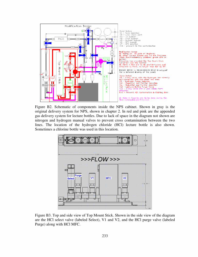
233
Figure B2. Schematic of components inside the NPS cabinet. Shown in gray is the
original delivery system for NPS, shown in chapter 2. In red and pink are the appended
gas delivery system for lecture bottles. Due to lack of space in the diagram not shown are
nitrogen and hydrogen manual valves to prevent cross contamination between the two
lines. The location of the hydrogen chloride (HCl) lecture bottle is also shown.
Sometimes a chlorine bottle was used in this location.
Figure B3. Top and side view of Top Mount Stick. Shown in the side view of the diagram
are the HCl select valve (labeled Select), V1 and V2, and the HCl purge valve (labeled
Purge) along with HCl MFC.

234
Functional Description of NPS Gas Panel:
The NPS gas panel is designed to allow for the flow of hydrogen either into the NPS
ampule or bypassing the NPS ampule. The hydrogen line to the NPS cabinet is teed-off
from the main hydrogen after the hydrogen purifier (see Figure B1). The Regulator is
used to control the pressure hydrogen going directly into the NPS ampule. This value is
typically set at 0 psig. A check value (CV1) is to prevent the backflow of NPS into the
hydrogen line. V2 is the leak check port for the gas panel. V6 is the NPS MFC bypass
value.
The hydrogen flows is as follows:
V1 (NPS panel) => Filter => CV1 => Regulator => Either V5 or (V3 =>NPS Ampule
=>V4) => NPS MFC => V7 => RTCVD Chamber Main or Vent (3-port value).
The NPS MFC is calibrated for DCS, so a calibration factor of 0.434 is used. The range
of the MFC is 300 sccm of DCS. A setting of 0.434 on the MFC corresponds to 300 sccm
of hydrogen.
NPS Gas Flow and NPS Panel Purge Instructions
Gas Flow
[1] Before any gas panel usage, follow the standard RTCVD startup procedure and
verify that the reactor and the Burnbox are in operational status with hydrogen
flowing (MFC =0.1) through the main chamber. All manual valves in the cabinet
should be closed.
[2] Flow hydrogen gas from the NPS panel by doing the following:
[2a] Open the Vent Valve, then open the Cabinet Vent Valve shown
connected to the vent line in the top view of Figure B1 above.
[2b] In DAQ Factory, set the NPS MFC to 1. Open V1, V5, and V7. The
chamber pressure reading should be 1.6 torr. Fully open the regulator to
flush the NPS lines. Toggle NPS Inject (DAQ factory) to flush the NPS
line to the RTCVD chamber.
[2c] Adjust the NPS MFC to your target gas flow (i.e.0.72 for 50 sccm of NPS
in hydrogen). Then adjust the regulator till the outlet pressure of the
regulator reads ~0 psig
[3] To flow NPS instead of hydrogen:
[3a] Leave V5 open and then open V4, wait for the pressure to stabilize
235
[3b] Open V3, then open the Outlet Ampule Valve (Not shown in Figure B2)
and then open the Inlet Ampule Valve
[3c] Close V5 (Due to the temporary clogging of the NPS MFC this step is not
done until 5 minutes before the NPS Inject in your recipe.
[4] You are now ready to run your recipe!
[5] When you recipe is complete close the two NPS Ampule Valves
Gas Purge
[6] Flush the lines with hydrogen after completion of recipe
[6a] Verify step [1] and verify that the NPS Ampule Valves are both
closed.(NPS gas panel manual values do not have to be closed)
[6b] Set NPS MFC to 1 and then open the manual valve shown connected to
the vent line in the top view of Figure B1 above.
[6c] Open V1, V4, V7 and fully open the Regulator
[6d] Open V2 and V3, then close V1
[6e] When Regulator reading is <-30 mmHg close V2 and V3
[6f] Cycle Steps 6c to 6e, 10 times
[7] When the purge is complete, reduce Regulator so that the outlet pressure reads 20
psig
[8] Close V7, then close V1 and V4, and follow standard RTCVD shutdown
procedures
[9] The next morning check the Regulator pressure (If it still reads 20 psig then there
is no leak) to see if there are any leaks in the NPS panel
Functional Description of Lecture Bottle Gas Panel:
The gas panel modification above is designed to inject the contents from a lecture bottle
(shown in green in Figure B2 above) into the existing reactor chamber via the use of top
mount (aka surface mount) technology to minimize the use of space. The lecture bottle
can be either HCl or Chlorine gas. The line connection to the lecture bottle is a CGA 660
fitting. The components of the Top Mount Stick are shown in Figure B3 above. All of the
valve on the surface mount are pneumatic valves, and are controlled by the DAQ factory
program. V1 and V2 are tied together and called HCl V1 in the DAQ factory program.
HCl Purge is the purge valve for the Top mount stick, and can flow either N2 or H2 gas.
HCl Select is a manual and pneumatic valve, where the valve is opened only when both
the manual and pneumatic valve is opened (See the top view of the select valve). The
HCl MFC is a 300sccm MFC with a 9-pin connection.

236
Lecture Bottle Gas Flow Instructions:
[1] Before any lecture bottle usage, follow the standard RTCVD startup procedure
and verify that the reactor and the Burnbox are in operational status with
hydrogen flowing (MFC =0.1) through the main chamber. All manual valves in
the cabinet should be closed.
[2] Open the Tank valve to the lecture bottle.
[3] Verify that V13 and V8 are closed (i.e. the T-direction of the 3-way valve is
closed. Open V10 and V11.
[4] Open the either the nitrogen or hydrogen manual valve (Open only one NOT
both!) on the panel to enable either N2 or H2 flow into the HCl line. Open V9.
[5] Flow gas from the lecture bottle by doing the following:
[5a] Open the Vent Valve, then open the Cabinet Vent Valve shown
connected to the vent line in the top view of Figure B1 above.
[5b] In DAQ Factory, set the HCl MFC to 1, then open HCl V1 and HCl V2
in the program. This will now flow H2 or N2 through the Top Mount Stick
and out to the vent line. The reactor pressure should be around 1.10 torr.
[5c] In DAQ Factory, click HCl Select (the line is now flowing HCl through
the Top Mount Stick up to V11). HCl is now flowing to vent.
[6] Turn off HCl Select, so that H2 or N2 is flowing through the Top Mount Stick
[7] You are now ready to run your recipe!
Lecture Bottle Change Instructions:
[1] Before any lecture bottle usage, follow the standard RTCVD startup procedure
and verify that the reactor and the Burnbox are in operational status with
hydrogen flowing (MFC =0.1) through the main chamber. All manual valves in
the cabinet should be closed.
[2] Close the Tank valve to the lecture bottle.
[3] Verify that V13 and V8 are closed (i.e. the T-direction of the 3-way valve is
closed. Also verify that V10 and V11 are closed.
[4] Open the either the nitrogen or hydrogen manual valve (Open only one NOT
both!) on the panel to enable either N2 or H2 flow into the HCl line. Open V9.
[5] Open the Vent Valve, then open the Cabinet Vent Valve shown connected to the
vent line in the top view of figure B1 above.
[6] Open V12 slowly, this will directly pump out the HCl in the line up to the lecture
bottle out through the vent, and pump out up to V10 on the other side of the line.
[7] When the RTCVD pressure reading is back down to 0.7, closed V12
[8] Open V8, the line is now pressurized with N2
[9] Close V8
[10] Cycle Steps 6-9 for 50 times.
[11] Open V8 so that the line is pressurized with N2
[12] Close V8, change Lecture Bottle then cycle steps 6-9 for 50 times.
[13] Leak check the new bottle by installing the leak checker onto the 3-port of V13
[14] Open V13 to leak check
[15] If the leak check is successful, cycle purge and flush the lines with N2 thoroughly
before opening the lecture bottle.

237
Appendix C
Hydrogen Desorption
This section is to explain hydrogen desorption in more detail. There are two types of
hydrogen desorption, called β1 (monohydride), and β2 (dihydride) desorption. At roughly
400oC (673
oK) dihydride desorption occurs, and the silicon surface transitions from a
dihydride surface (Si: 1x1) reconstruction, with 2 hydrogen atoms per surface silicon
atom to a monohydride surface (one hydrogen atom per silicon surface atom). The
surface silicon atom now has an empty bond that will pair with its nearest neighbor
reconstructing the silicon surface into a Si: 2x1 surface. Monohydride desorption occurs
around 510oC (783
oK), at temperatures higher than 510
oC all of the hydrogen on the
surface will desorb and the surface will be a perfect 2x1 reconstruction. The β1 and β2
peaks are shown in Figure C1 below:
Figure C1. Experimental and fitted TPD spectra of D2 from Si(001) surfaces initially
dosed with (a) 1.09 and (b) 1.31 ML atomic deuterium [4.8].
Both the experimental (circles) and fitted (dashed line) TPD spectra of deuterium are
shown. Note that in (b) of figure C1, the β2 peak is higher as there are more dihydride
phases on the silicon lattice than in (a). The monohydride peak is also higher than the
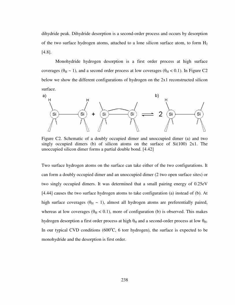
238
dihydride peak. Dihydride desorption is a second-order process and occurs by desorption
of the two surface hydrogen atoms, attached to a lone silicon surface atom, to form H2
[4.8].
Monohydride hydrogen desorption is a first order process at high surface
coverages (θH ~ 1), and a second order process at low coverages (θH < 0.1). In Figure C2
below we show the different configurations of hydrogen on the 2x1 reconstructed silicon
surface.
Figure C2. Schematic of a doubly occupied dimer and unoccupied dimer (a) and two
singly occupied dimers (b) of silicon atoms on the surface of Si(100) 2x1. The
unoccupied silicon dimer forms a partial double bond. [4.42]
Two surface hydrogen atoms on the surface can take either of the two configurations. It
can form a doubly occupied dimer and an unoccupied dimer (2 two open surface sites) or
two singly occupied dimers. It was determined that a small pairing energy of 0.25eV
[4.44] causes the two surface hydrogen atoms to take configuration (a) instead of (b). At
high surface coverages (θH ~ 1), almost all hydrogen atoms are preferentially paired,
whereas at low coverages (θH < 0.1), more of configuration (b) is observed. This makes
hydrogen desorption a first order process at high θH and a second-order process at low θH.
In our typical CVD conditions (600oC, 6 torr hydrogen), the surface is expected to be
monohydride and the desorption is first order.

239
Appendix D
Terrace-Step-Kink Model
Figure D1. Schematic showing the different positions of an adatom, based on the
Terrace-Step-Kink Model for a simple cubic lattice. Picture taken from Wikipedia.com.
The Terrace-Step-Kink model is based upon the idea that position of an adatom on the
crystal surface is determined by its bonding to neighboring atoms and that transitions
simply involve the counting of broken and formed bonds. Below is a table of the possible
positions of an adatom and the number of broken bonds and formed bonds for each
position.
Table D1: Possible positions of the adatom and the number of broken and formed bonds
for a simple cubic lattice based on Figure D1.
# of Broken Bonds # of Formed Bonds
Adatom 5 1
Step Adatom 4 2
Kink Atom 3 3
Step Atom 2 4
Surface Atom 1 5
The adatom diffuses on the surface to minimize its energy by landing on the step, kink or
onto the (sub)surface. Based on table D1, we find that the adatom would want to diffuse
to the steps if possible. However if another adatom landed on top of the diffusing adatom,

240
it would become less mobile due to the lowered energy from having more bonds. The
silicon surface is not cubic, but it is expected that the concepts of the model could be
extended to the silicon surface.

241
Appendix E
SIMS Sample 4850 and Sample 4866
Figure E1. SIMS of sample 4050 grown with disilane at 6 torr with 3 slpm hydrogen
carrier.
Figure E2. SIMS of sample 4066 grown with NPS and silane at 6 torr with 3 slpm
hydrogen carrier. The layers grown with NPS are easily distinguishable due to the high
carbon background.
![Structure and functional properties of epitaxial PbZrxTi O3 films...epitaxial films[11][12]. Once the high quality epitaxial PZT films are made these can be used to better understand](https://static.fdocuments.us/doc/165x107/60df425bb5812e17d635303f/structure-and-functional-properties-of-epitaxial-pbzrxti-o3-films-epitaxial.jpg)