Chapter 4: Combinational Logic Dr Mohamed Menacer Taibah University 2007-2008.
44
Chapter 4: Chapter 4: Combinational Combinational Logic Logic Dr Mohamed Menacer Dr Mohamed Menacer Taibah University Taibah University 2007-2008 2007-2008
-
Upload
jamal-shepley -
Category
Documents
-
view
223 -
download
1
Transcript of Chapter 4: Combinational Logic Dr Mohamed Menacer Taibah University 2007-2008.

Chapter 4:Chapter 4:Combinational LogicCombinational Logic
Dr Mohamed MenacerDr Mohamed MenacerTaibah UniversityTaibah University
2007-20082007-2008

MultiplexerMultiplexer
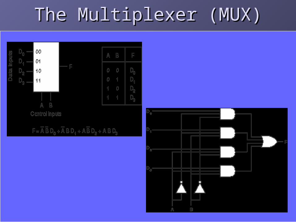
The Multiplexer (MUX)The Multiplexer (MUX)
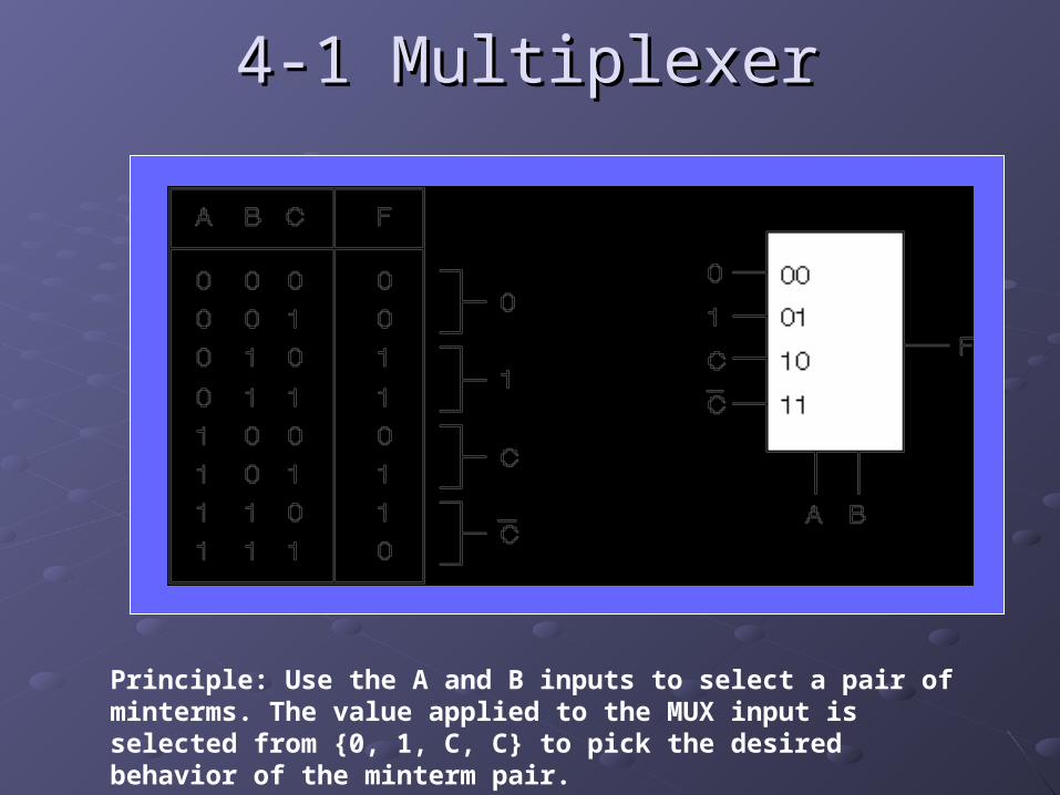
4-1 Multiplexer4-1 Multiplexer
Principle: Use the A and B inputs to select a pair of minterms. The value applied to the MUX input is selected from {0, 1, C, C} to pick the desired behavior of the minterm pair.
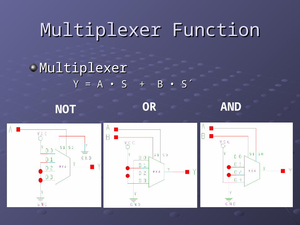
Multiplexer FunctionMultiplexer Function
MultiplexerMultiplexerY = A • S + B • S´Y = A • S + B • S´
NOT OR AND
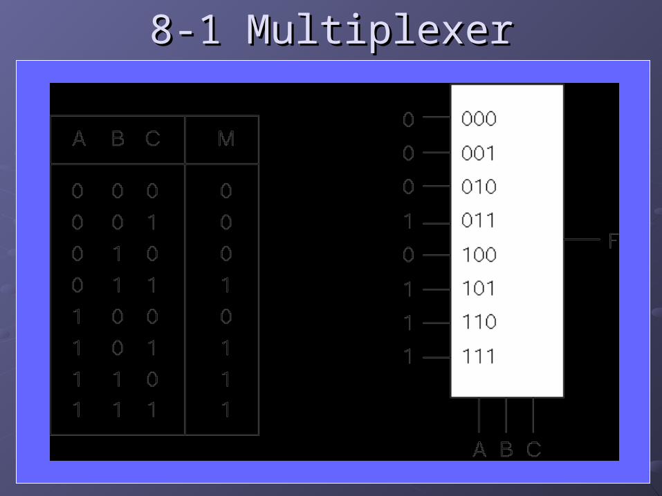
8-1 Multiplexer8-1 Multiplexer
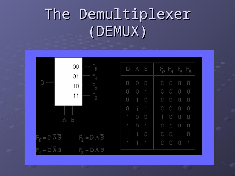
The Demultiplexer (DEMUX)The Demultiplexer (DEMUX)
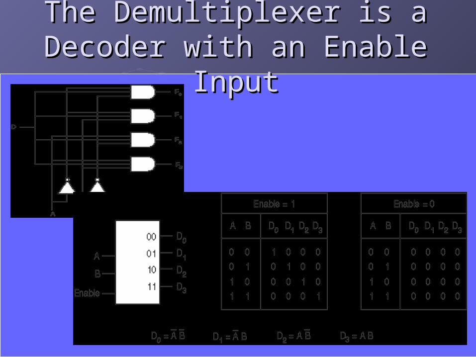
The Demultiplexer is a Decoder The Demultiplexer is a Decoder with an Enable Inputwith an Enable Input

AddersAdders
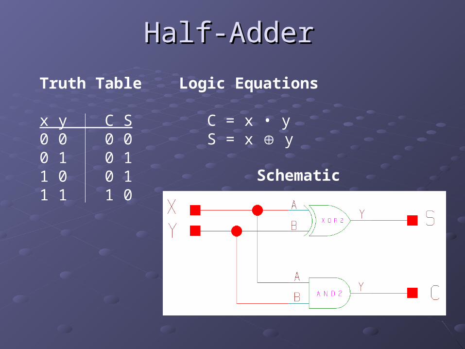
Half-AdderHalf-Adder
Logic Equations
C = x • y S = x y
Truth Table
x y C S0 0 0 00 1 0 11 0 0 11 1 1 0
Schematic
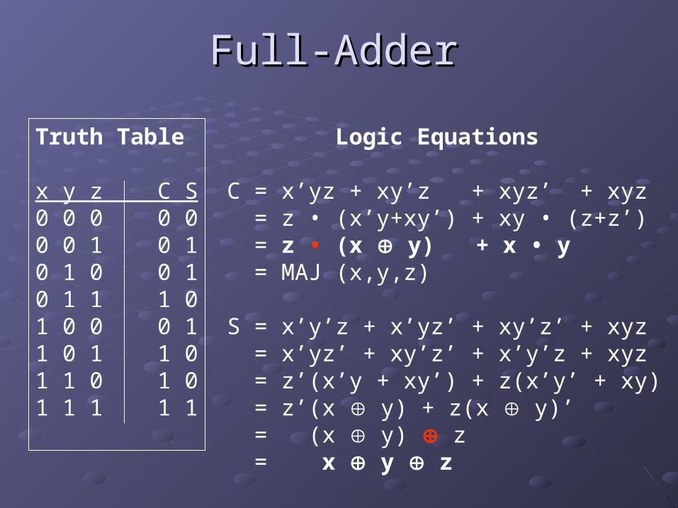
Full-AdderFull-Adder
Logic Equations
C = x’yz + xy’z + xyz’ + xyz = z • (x’y+xy’) + xy • (z+z’) = z • (x y) + x • y = MAJ (x,y,z)
S = x’y’z + x’yz’ + xy’z’ + xyz = x’yz’ + xy’z’ + x’y’z + xyz = z’(x’y + xy’) + z(x’y’ + xy) = z’(x y) + z(x y)’ = (x y) z = x y z
Truth Table
x y z C S0 0 0 0 00 0 1 0 10 1 0 0 10 1 1 1 01 0 0 0 11 0 1 1 01 1 0 1 01 1 1 1 1
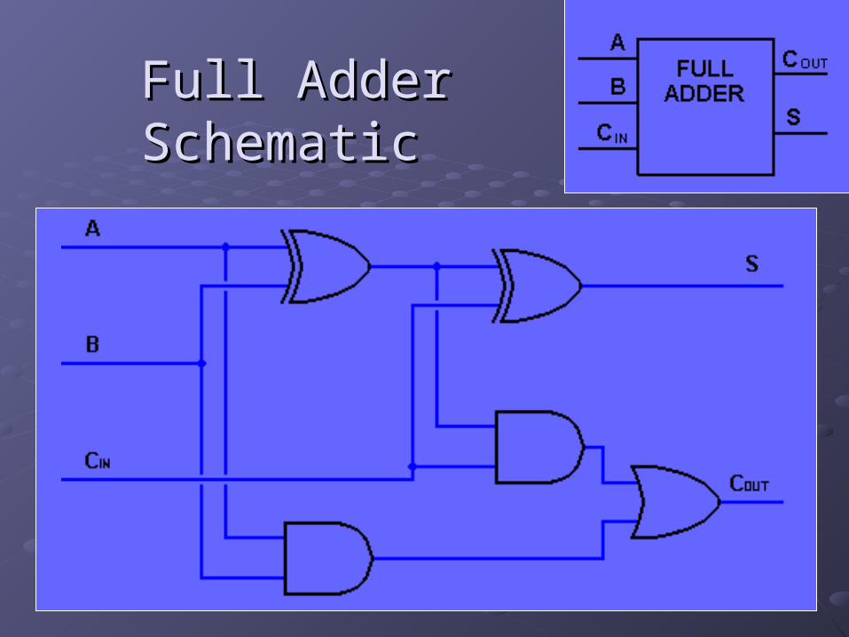
Full Adder SchematicFull Adder Schematic
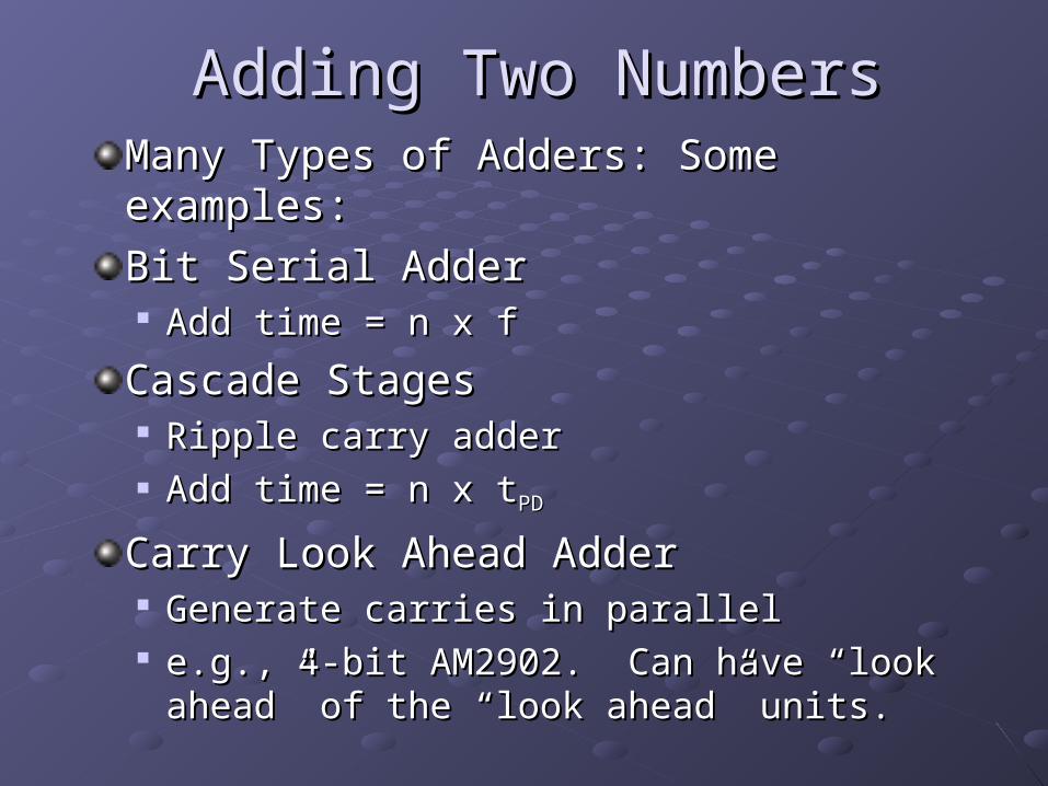
Adding Two NumbersAdding Two NumbersMany Types of Adders: Some examples:Many Types of Adders: Some examples:
Bit Serial AdderBit Serial Adder Add time = n x fAdd time = n x f
Cascade StagesCascade Stages Ripple carry adderRipple carry adder Add time = n x tAdd time = n x tPDPD
Carry Look Ahead AdderCarry Look Ahead Adder Generate carries in parallelGenerate carries in parallel e.g., 4-bit AM2902. Can have “look ahead” e.g., 4-bit AM2902. Can have “look ahead”
of the “look ahead” units.of the “look ahead” units.
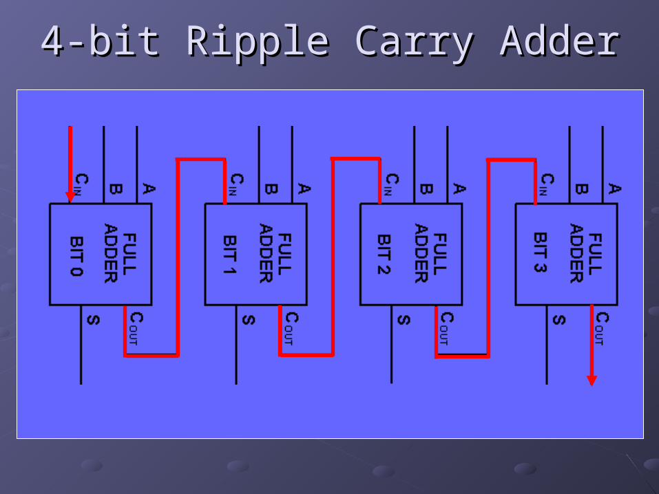
4-bit Ripple Carry Adder4-bit Ripple Carry Adder
Negative Numbers and SubtractionNegative Numbers and Subtraction
Several different codes for negative numbersSeveral different codes for negative numbers 2's complement2's complement 1's complement1's complement signed magnitudesigned magnitude othersothers
For 2's complement, subtraction is implemented For 2's complement, subtraction is implemented with the same hardware by negating the with the same hardware by negating the subtrahend. This is done by inverting each bit and subtrahend. This is done by inverting each bit and adding one. The one can be added by setting the adding one. The one can be added by setting the carry-in to the first stage equal to 1, saving an carry-in to the first stage equal to 1, saving an operation.operation.
DecodersDecoders
Decoder FundamentalsDecoder Fundamentals
Route data to one specific output line.Route data to one specific output line.
Selection of devices, resourcesSelection of devices, resources
Code conversions.Code conversions.
Arbitrary switching functionsArbitrary switching functions implements the AND planeimplements the AND plane
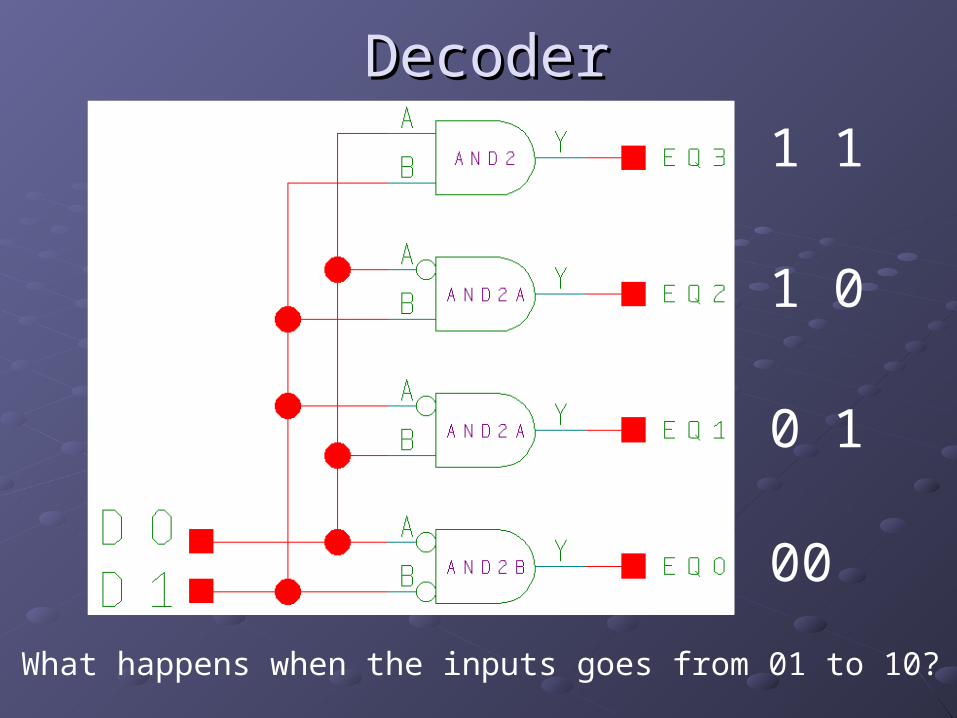
DecoderDecoder
1 1
1 0
0 1
00
What happens when the inputs goes from 01 to 10?
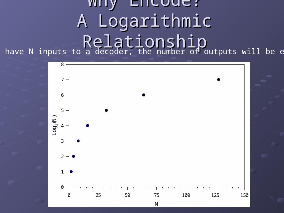
Why Encode?Why Encode?A Logarithmic RelationshipA Logarithmic Relationship
N
0 25 50 75 100 125 150
Log
2(N
)
0
1
2
3
4
5
6
7
8
Lets say we have N inputs to a decoder, the number of outputs will be equal to 2^N
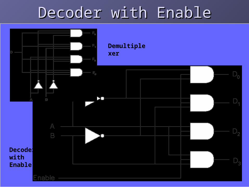
Decoder with EnableDecoder with Enable
Demultiplexer
Decoder with Enable
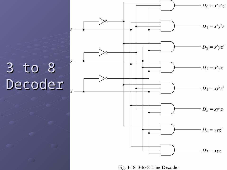
3 to 8 3 to 8 DecoderDecoder
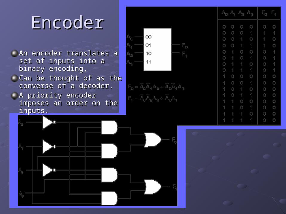
EncoderEncoder
An encoder translates a set An encoder translates a set of inputs into a binary of inputs into a binary encoding, encoding, Can be thought of as the Can be thought of as the converse of a decoder. converse of a decoder. A priority encoder imposes A priority encoder imposes an order on the inputs.an order on the inputs.
Sequential LogicSequential Logic
Sequential LogicSequential Logic
The combinational logic circuits we have The combinational logic circuits we have been studying so far have no memory. been studying so far have no memory. The outputs always follow the inputs.The outputs always follow the inputs.
There is a need for circuits with a memory, There is a need for circuits with a memory, which behave differently which behave differently depending upon depending upon their previous state.their previous state.
Sequential circuits use current input Sequential circuits use current input variables and previous input variables by variables and previous input variables by storing the information and putting back storing the information and putting back into the circuit on the next clock into the circuit on the next clock (activation) cycle. (activation) cycle.
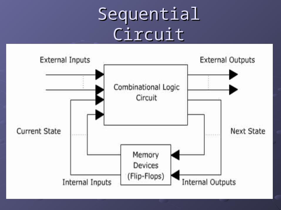
Sequential CircuitSequential Circuit
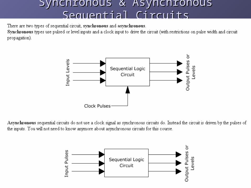
Synchronous & Asynchronous Sequential CircuitsSynchronous & Asynchronous Sequential Circuits
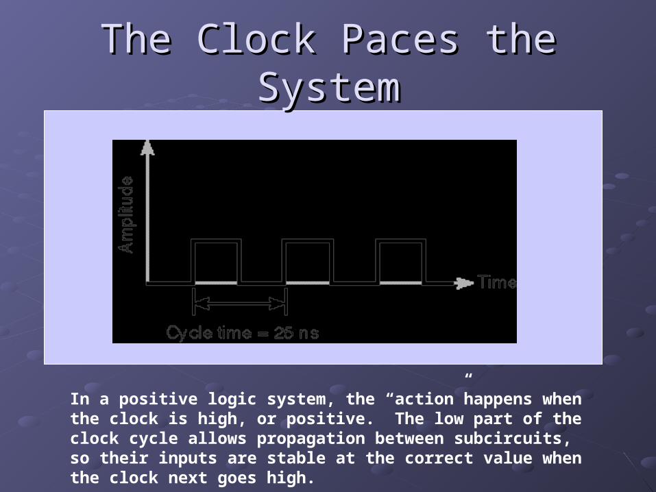
The Clock Paces the SystemThe Clock Paces the System
In a positive logic system, the “action”happens when the clock is high, or positive. The low part of the clock cycle allows propagation between subcircuits, so their inputs are stable at the correct value when the clock next goes high.
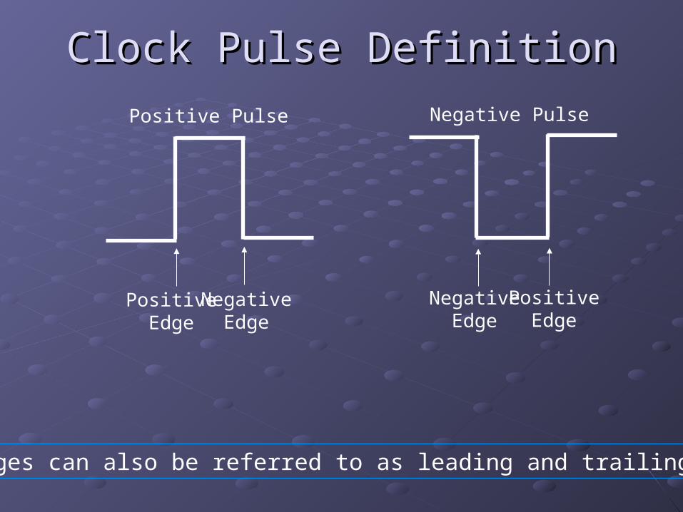
Clock Pulse DefinitionClock Pulse Definition
Edges can also be referred to as leading and trailing.
Positive Pulse
PositiveEdge
NegativeEdge
Negative Pulse
PositiveEdge
NegativeEdge
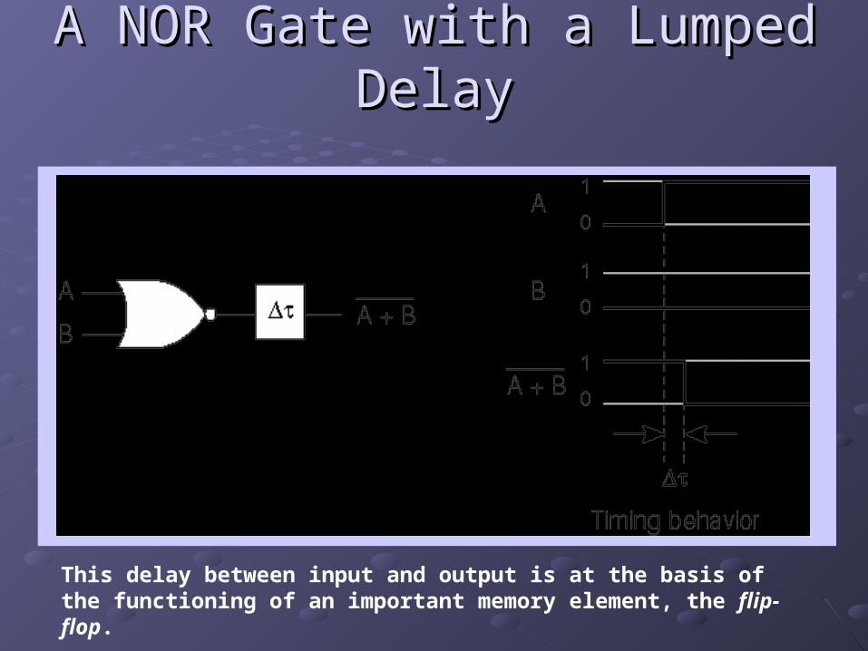
A NOR Gate with a Lumped A NOR Gate with a Lumped DelayDelay
This delay between input and output is at the basis of the functioning of an important memory element, the flip-flop.
Flip-FlopsFlip-Flops
Flip-flops are the first stage in sequential logic design which incorporates memory (storage of previous states).
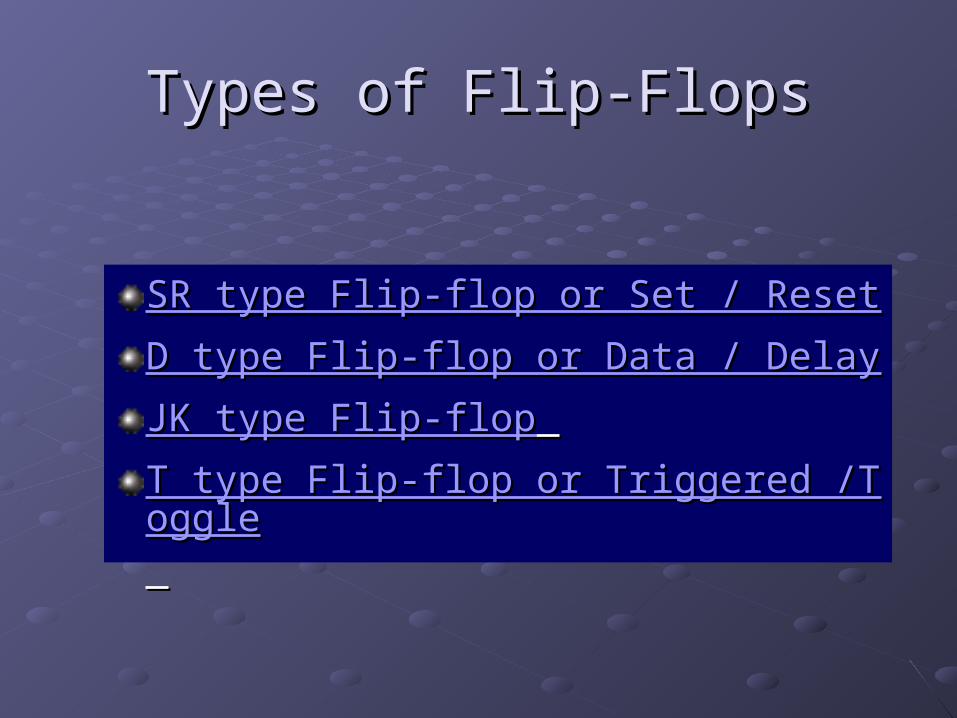
Types of Flip-FlopsTypes of Flip-Flops
SR type Flip-flop or Set / ResetSR type Flip-flop or Set / Reset
D type Flip-flop or Data / DelayD type Flip-flop or Data / Delay
JK type Flip-flopJK type Flip-flop
T type Flip-flop or Triggered /ToggleT type Flip-flop or Triggered /Toggle

The S-R (Set-Reset) Flip-FlopThe S-R (Set-Reset) Flip-Flop
The S-R flip-flop is an active high (positive logic) device.
The operation of an SR flip-flop is as follows: The Set input will make Q goto 1 The Reset input will make the output Q goto 0 i.e. reset the output.Both Set and Reset at logic 1 is not allowed as this is not a logical pair of inputs.
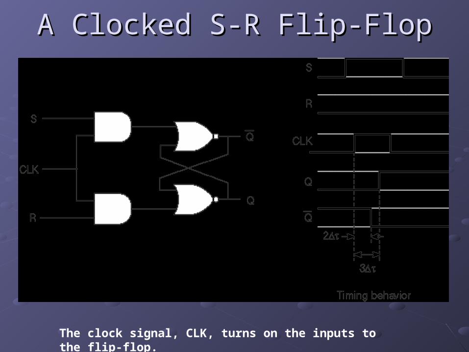
A Clocked S-R Flip-FlopA Clocked S-R Flip-Flop
The clock signal, CLK, turns on the inputs to the flip-flop.
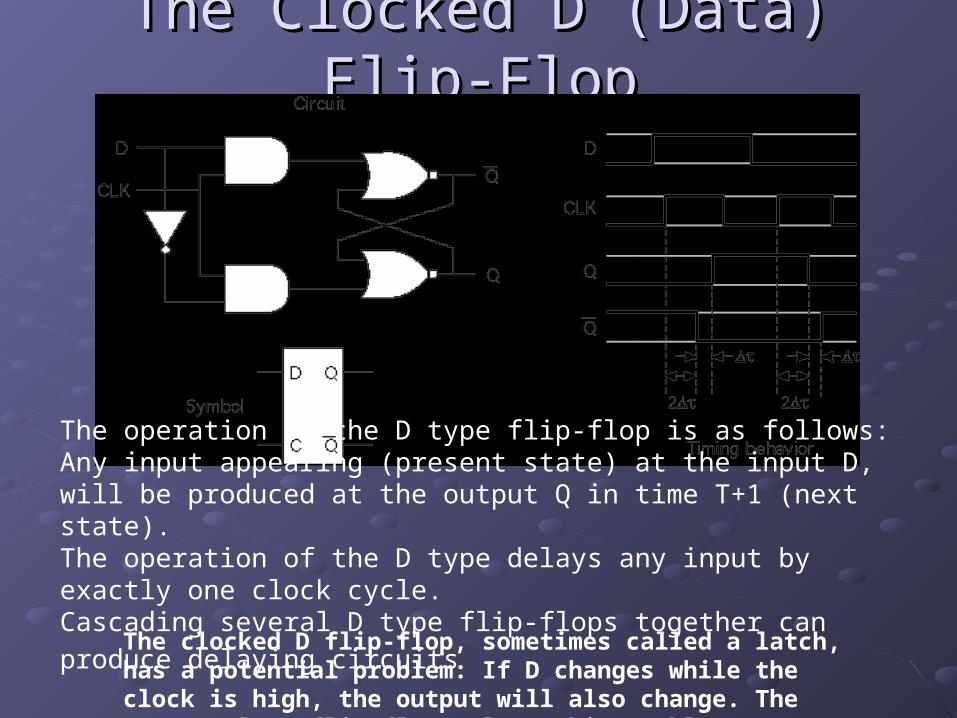
The Clocked D (Data) Flip-FlopThe Clocked D (Data) Flip-Flop
The clocked D flip-flop, sometimes called a latch, has a potential problem: If D changes while the clock is high, the output will also change. The Master-Slave flip-flop solves this problem:
The operation of the D type flip-flop is as follows: Any input appearing (present state) at the input D, will be produced at the output Q in time T+1 (next state). The operation of the D type delays any input by exactly one clock cycle.Cascading several D type flip-flops together can produce delaying circuits
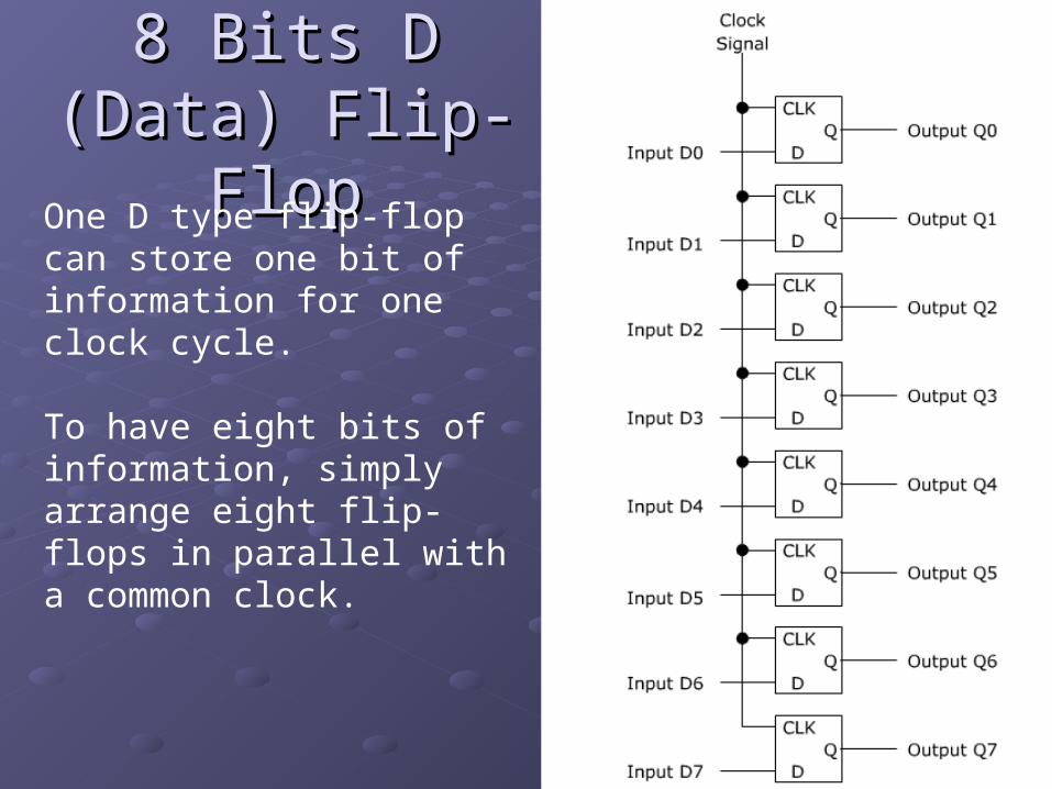
8 Bits D (Data) 8 Bits D (Data) Flip-FlopFlip-Flop
One D type flip-flop can store one bit of information for one clock cycle.
To have eight bits of information, simply arrange eight flip-flops in parallel with a common clock.

The Master-Slave Flip-FlopThe Master-Slave Flip-Flop
The rising edge of the clock clocks new data into the Master, while the slave holds previous data. The falling edge clocks the new Master data into the Slave.

Parallel RegistersParallel Registers
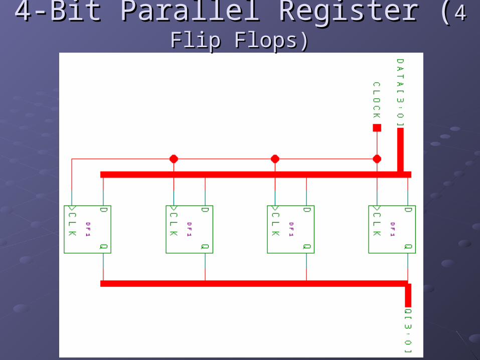
4-Bit Parallel Register (4-Bit Parallel Register (4 Flip Flops)4 Flip Flops)
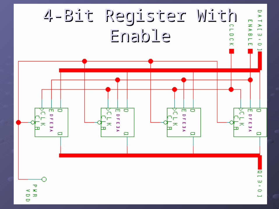
4-Bit Register With Enable4-Bit Register With Enable

Memory DevicesMemory Devices
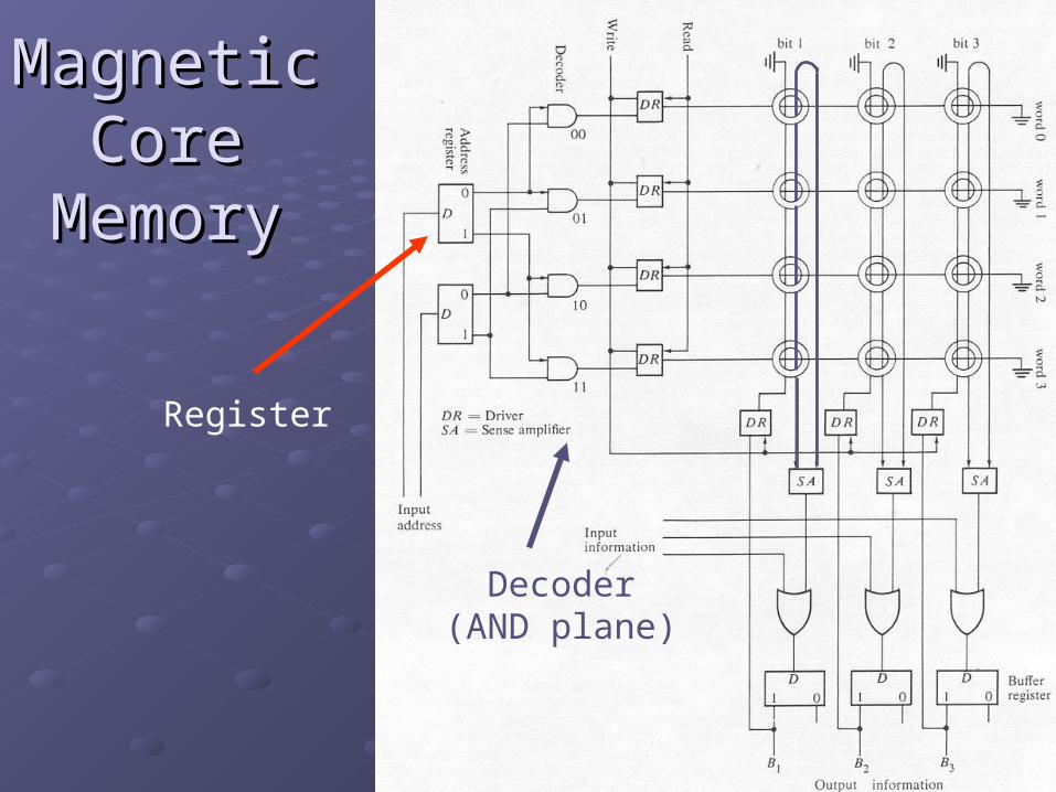
Register
MagneticMagneticCoreCore
MemoryMemory
Decoder(AND plane)
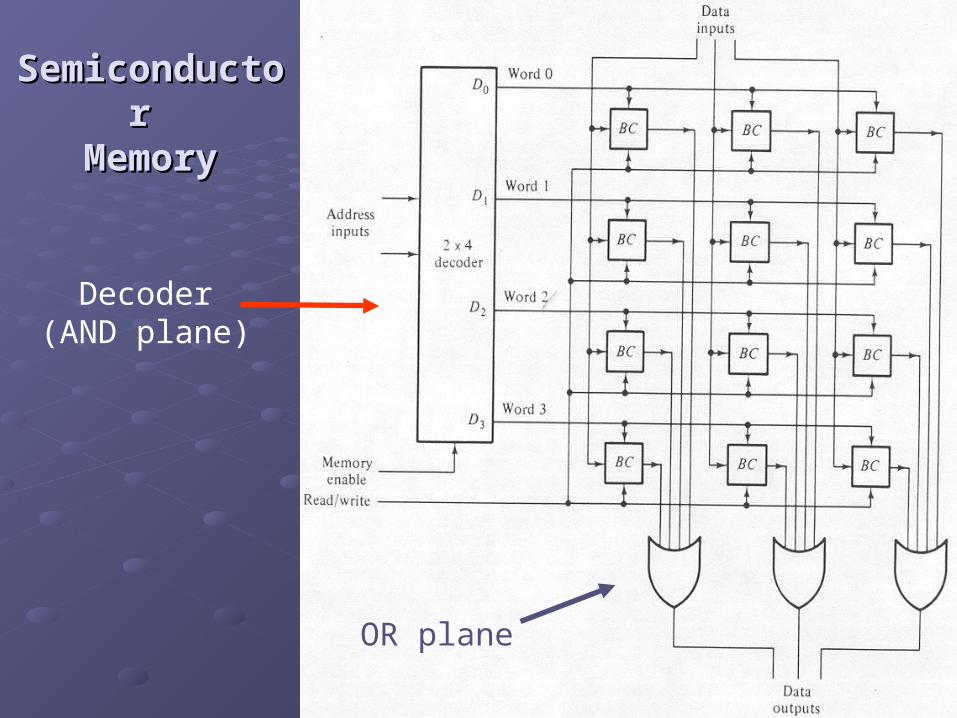
Semiconductor Semiconductor MemoryMemory
Decoder(AND plane)
OR plane

UT4090 RAM ModuleUT4090 RAM Module
Dual-portDual-port
1152 bits per cell1152 bits per cell
Four Four configurationsconfigurations 64 X 1864 X 18 128 X 9128 X 9 256 X 4256 X 4 512 X 2512 X 2
WA(8:0)
WD(17:0)
WE
WCLK
MODE(1:0)
RE
RCLK
RA(8:0)
RD(17:0)
ASYNCRD
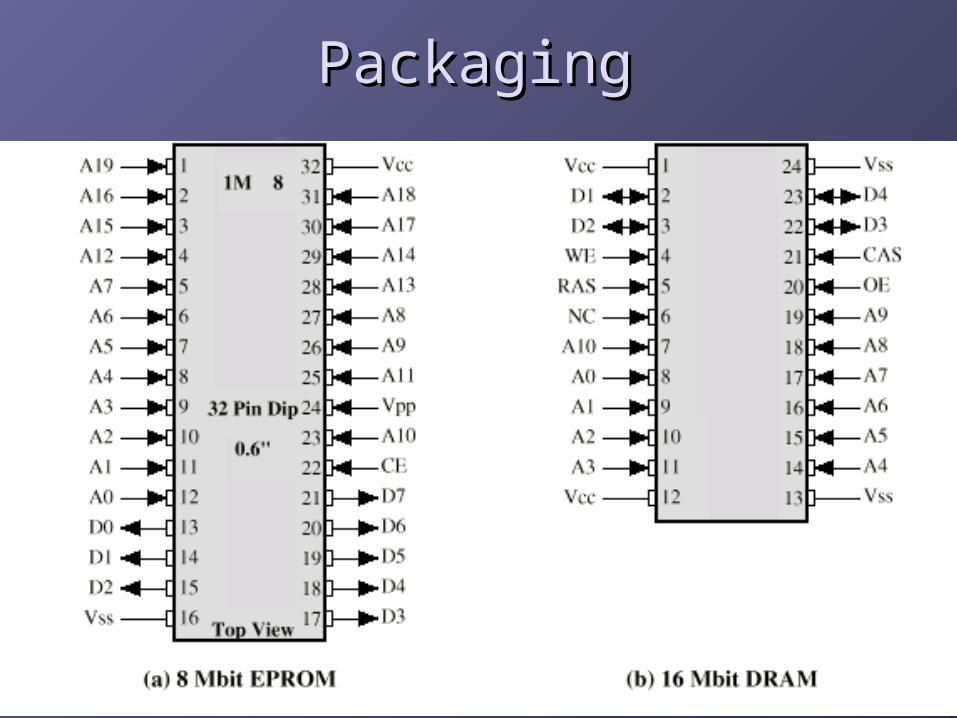
PackagingPackaging