Chapter 4 · 2 4.6 Memory Organization • Computer memory consists of a linear array of...
161
Chapter 4 MARIE: An Introduction to a Simple Computer
Transcript of Chapter 4 · 2 4.6 Memory Organization • Computer memory consists of a linear array of...
Chapter 4
MARIE: An Introduction
to a Simple Computer
2
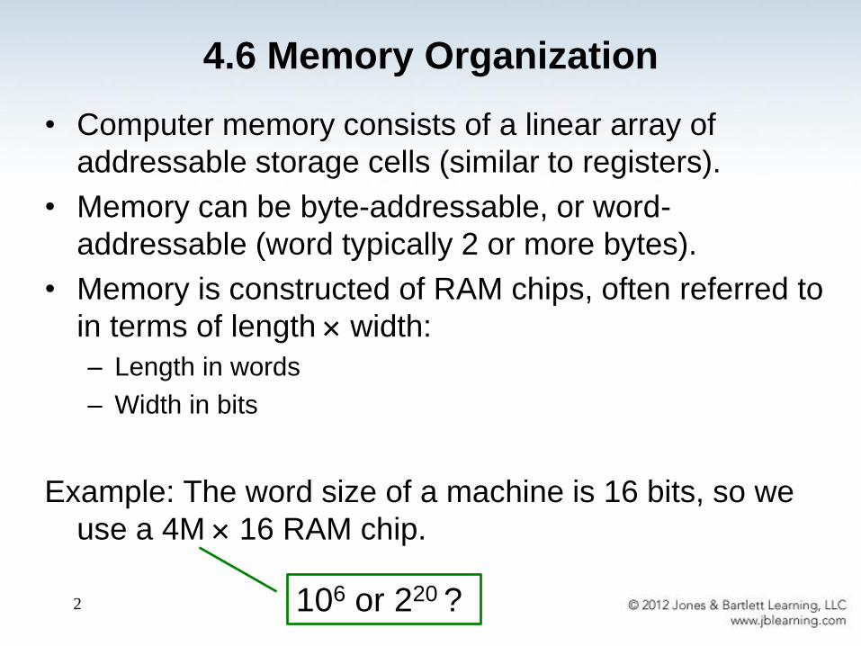
4.6 Memory Organization
• Computer memory consists of a linear array of
addressable storage cells (similar to registers).
• Memory can be byte-addressable, or word-
addressable (word typically 2 or more bytes).
• Memory is constructed of RAM chips, often referred to
in terms of length width:
– Length in words
– Width in bits
Example: The word size of a machine is 16 bits, so we
use a 4M 16 RAM chip.
106 or 220 ?
3
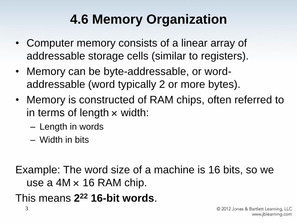
4.6 Memory Organization
• Computer memory consists of a linear array of
addressable storage cells (similar to registers).
• Memory can be byte-addressable, or word-
addressable (word typically 2 or more bytes).
• Memory is constructed of RAM chips, often referred to
in terms of length width:
– Length in words
– Width in bits
Example: The word size of a machine is 16 bits, so we
use a 4M 16 RAM chip.
This means 222 16-bit words.
4
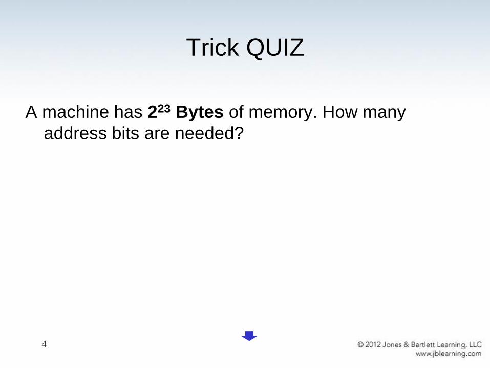
Trick QUIZ
A machine has 223 Bytes of memory. How many
address bits are needed?
5
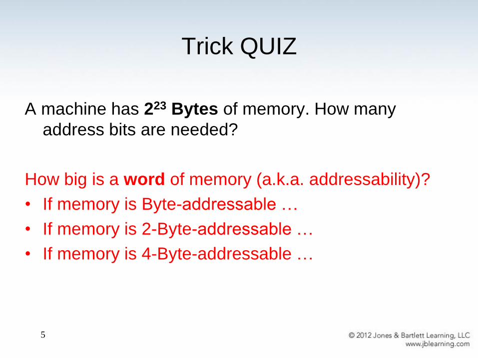
Trick QUIZ
A machine has 223 Bytes of memory. How many
address bits are needed?
How big is a word of memory (a.k.a. addressability)?
• If memory is Byte-addressable …
• If memory is 2-Byte-addressable …
• If memory is 4-Byte-addressable …

Do not get confused!
The width of memory chips is always given in bits.
E.g. this chip:
“ 64K x 8, byte-addressable ”
It means “ (64 x 1024)-long x 8 bits-wide,
addressable at the byte level “
6
7
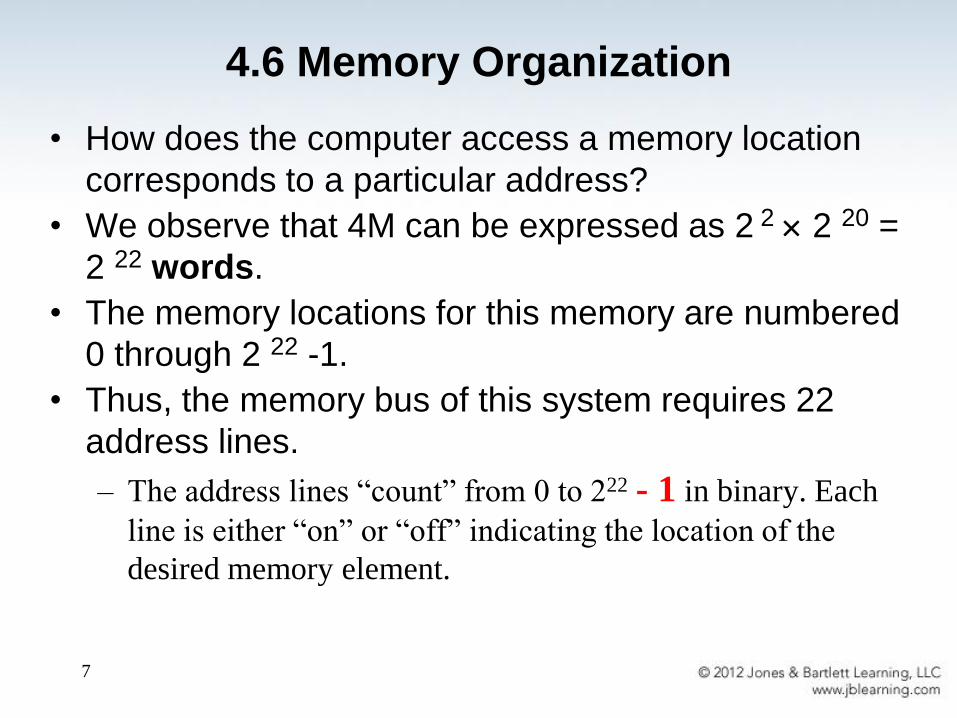
• How does the computer access a memory location
corresponds to a particular address?
• We observe that 4M can be expressed as 2 2 2 20 =
2 22 words.
• The memory locations for this memory are numbered
0 through 2 22 -1.
• Thus, the memory bus of this system requires 22
address lines.
– The address lines “count” from 0 to 222 - 1 in binary. Each
line is either “on” or “off” indicating the location of the
desired memory element.
4.6 Memory Organization

8
The memory bus of this system requires at least 22
address lines.
– The address lines “count” from 0 to 222 - 1 in binary. Each
line is either “on” or “off” indicating the location of the
desired memory element.
If the addresses are written in hex, what is the range
of addresses available in this machine?
QUIZ
9
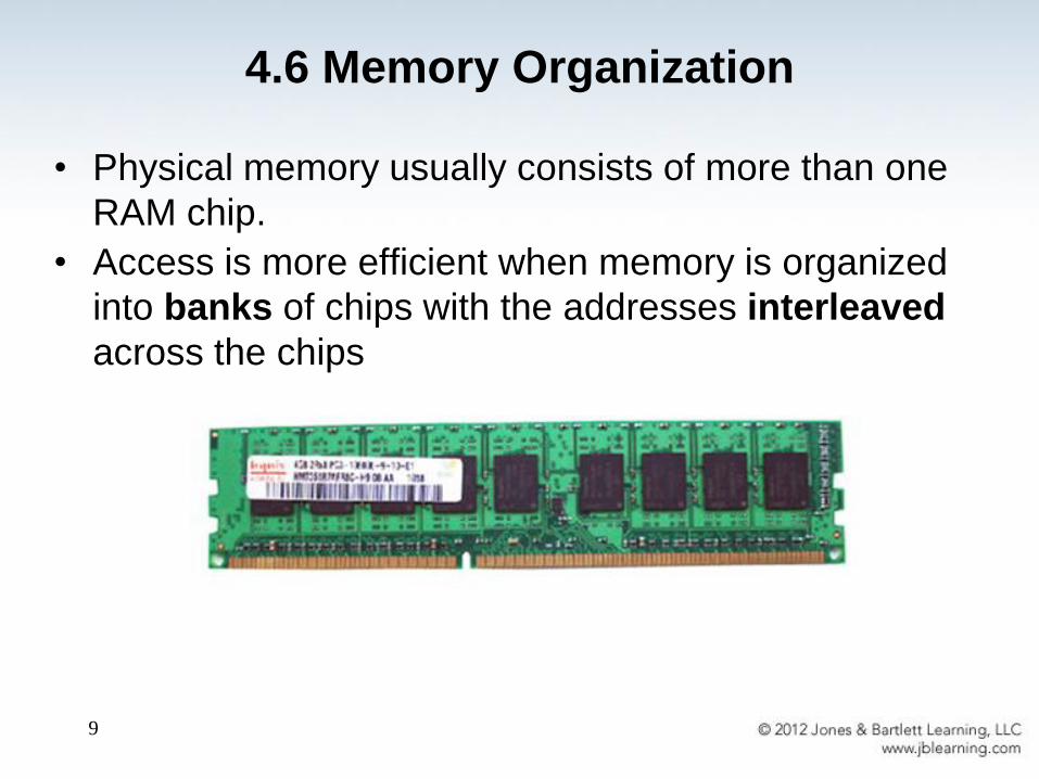
• Physical memory usually consists of more than one
RAM chip.
• Access is more efficient when memory is organized
into banks of chips with the addresses interleaved
across the chips
4.6 Memory Organization
10
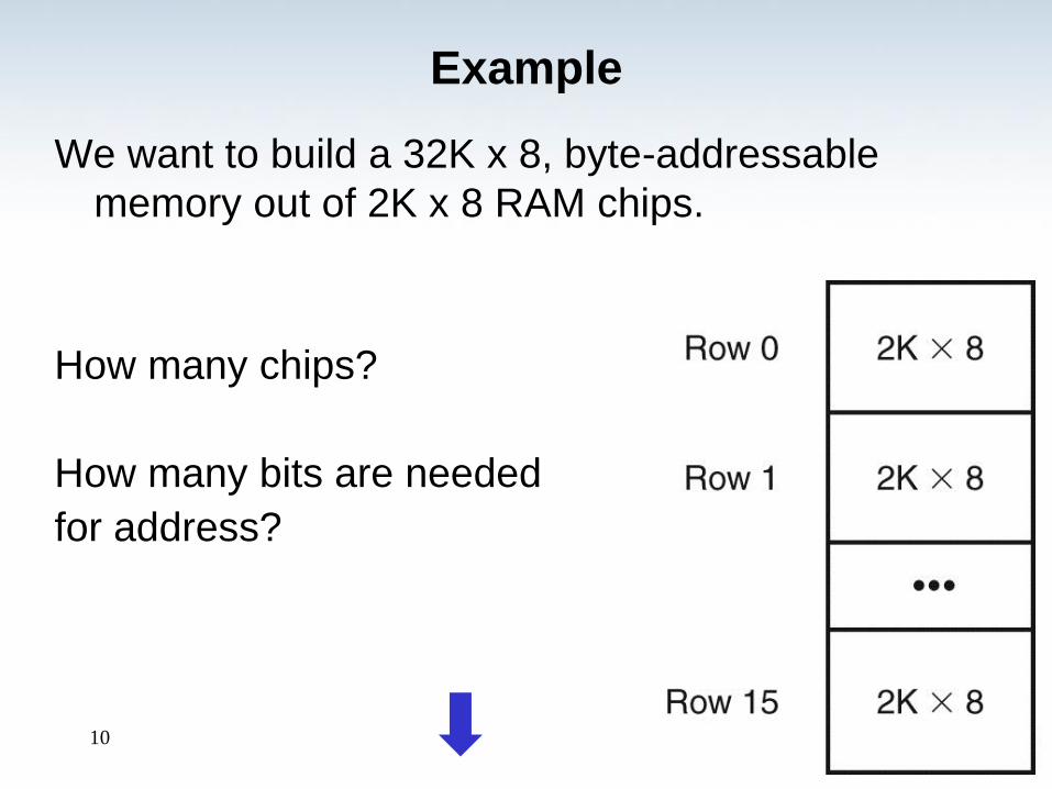
We want to build a 32K x 8, byte-addressable
memory out of 2K x 8 RAM chips.
How many chips?
How many bits are needed
for address?
Example
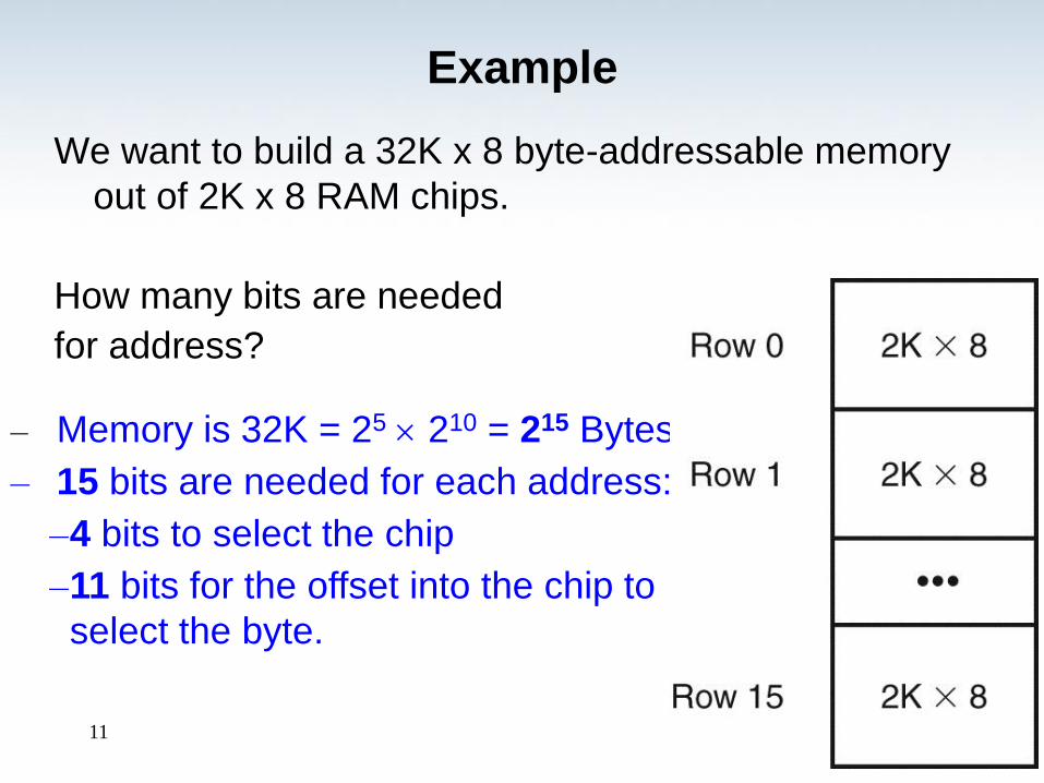
11
We want to build a 32K x 8 byte-addressable memory
out of 2K x 8 RAM chips.
How many bits are needed
for address?
Example
– Memory is 32K = 25 210 = 215 Bytes
– 15 bits are needed for each address:
–4 bits to select the chip
–11 bits for the offset into the chip to
select the byte.

12
We want to build a 32K x 16 memory out of 2K x 8
RAM chips.
How many chips?
How many bits are needed
for address?
Example
We call it word-addressable
13
We want to build a 32K x 16 memory out of 2K x 8
RAM chips.
How many bits are needed
for address?
Example
– Memory is 32K x2 = 25 210 2= 216
Bytes
– But still only 15 bits are needed for each
address:
– 4 bits to select the row of chips
– 11 bits for the offset into the chip to
select the byte.
Wait a second, aren’t we missing a factor of 2? (One bit?)

14
We want to build a 32K x 16 memory out of 2K x 8
RAM chips.
How many bits are needed
for address?
Example
– Memory is 32K x2 = 25 210 2= 216
Bytes
– But still only 15 bits are needed for each
address:
– 4 bits to select the row of chips
– 11 bits for the offset into the chip to
select the byte.
All 16 bits at an address are activated by the same address! The difference is
only in the data bus, which is now 16 bits wide!
15
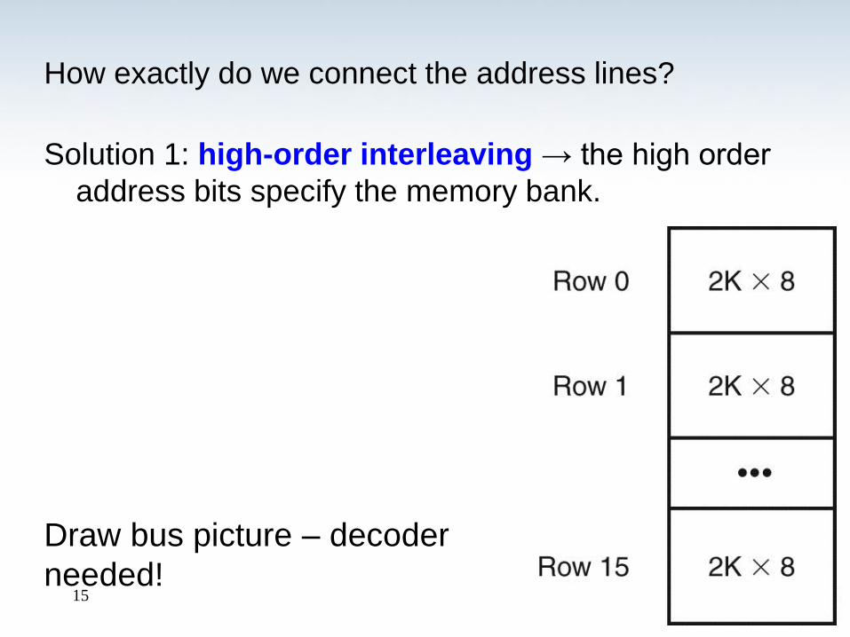
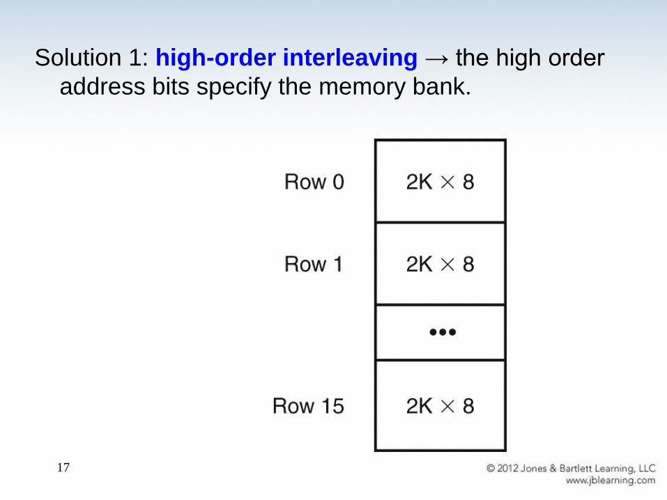
How exactly do we connect the address lines?
Solution 1: high-order interleaving → the high order
address bits specify the memory bank.
Draw bus picture – decoder
needed!
16
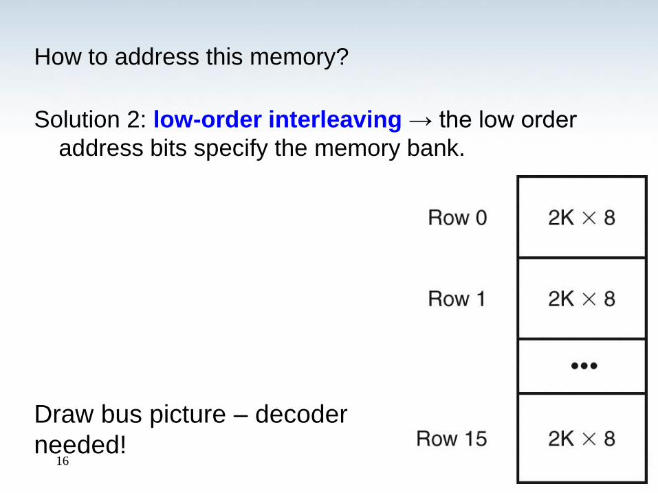
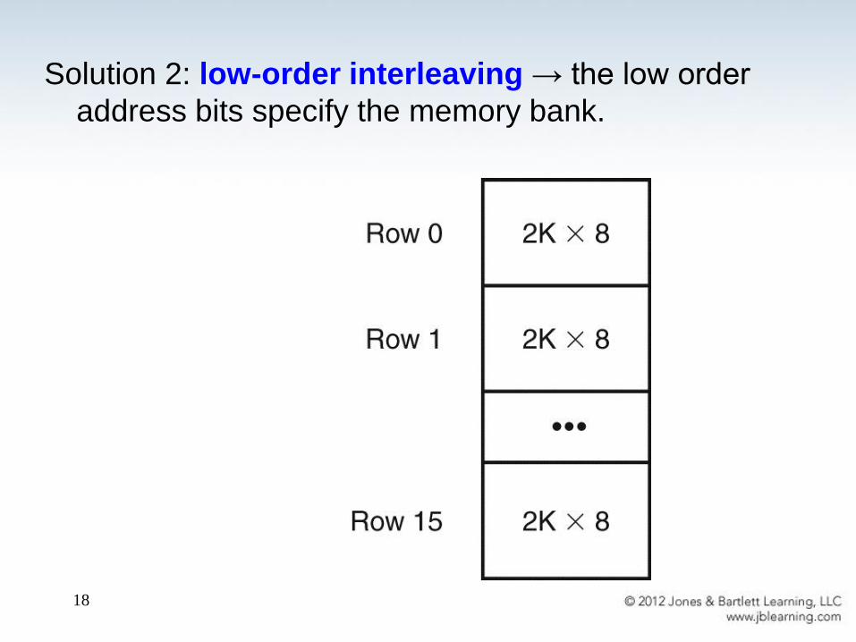
How to address this memory?
Solution 2: low-order interleaving → the low order
address bits specify the memory bank.
Draw bus picture – decoder
needed!
17
Solution 1: high-order interleaving → the high order
address bits specify the memory bank.
18
Solution 2: low-order interleaving → the low order
address bits specify the memory bank.
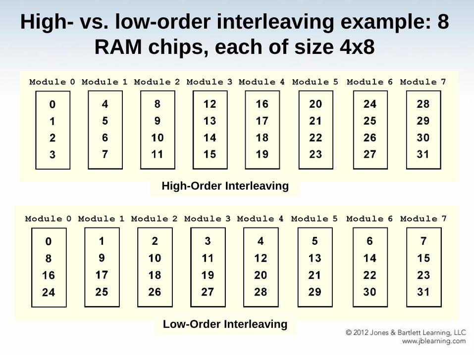
Low-Order Interleaving
High-Order Interleaving
High- vs. low-order interleaving example: 8
RAM chips, each of size 4x8
High-Order Interleaving
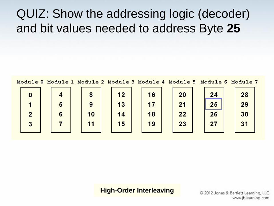
QUIZ: Show the addressing logic (decoder)
and bit values needed to address Byte 25
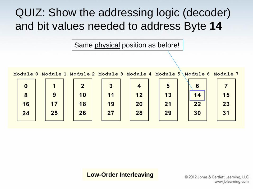
Low-Order Interleaving
QUIZ: Show the addressing logic (decoder)
and bit values needed to address Byte 14
Same physical position as before!
22
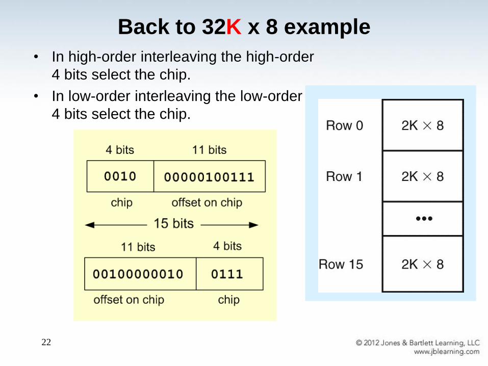
Back to 32K x 8 example
• In high-order interleaving the high-order
4 bits select the chip.
• In low-order interleaving the low-order
4 bits select the chip.
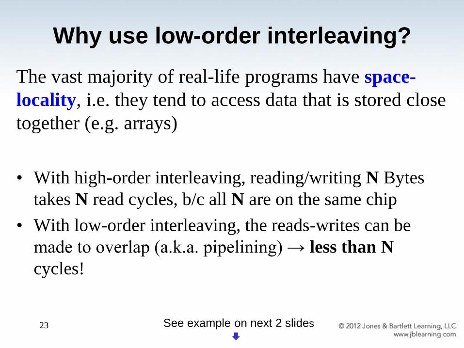
Why use low-order interleaving?
The vast majority of real-life programs have space-
locality, i.e. they tend to access data that is stored close
together (e.g. arrays)
• With high-order interleaving, reading/writing N Bytes
takes N read cycles, b/c all N are on the same chip
• With low-order interleaving, the reads-writes can be
made to overlap (a.k.a. pipelining) → less than N
cycles!
23 See example on next 2 slides
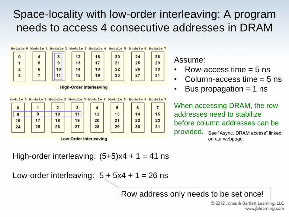
Space-locality with low-order interleaving: A program
needs to access 4 consecutive addresses in DRAM
Assume:
• Row-access time = 5 ns
• Column-access time = 5 ns
• Bus propagation = 1 ns
When accessing DRAM, the row
addresses need to stabilize
before column addresses can be
provided.
High-order interleaving: (5+5)x4 + 1 = 41 ns
Low-order interleaving: 5 + 5x4 + 1 = 26 ns
Row address only needs to be set once!
See “Async. DRAM access” linked
on our webpage.
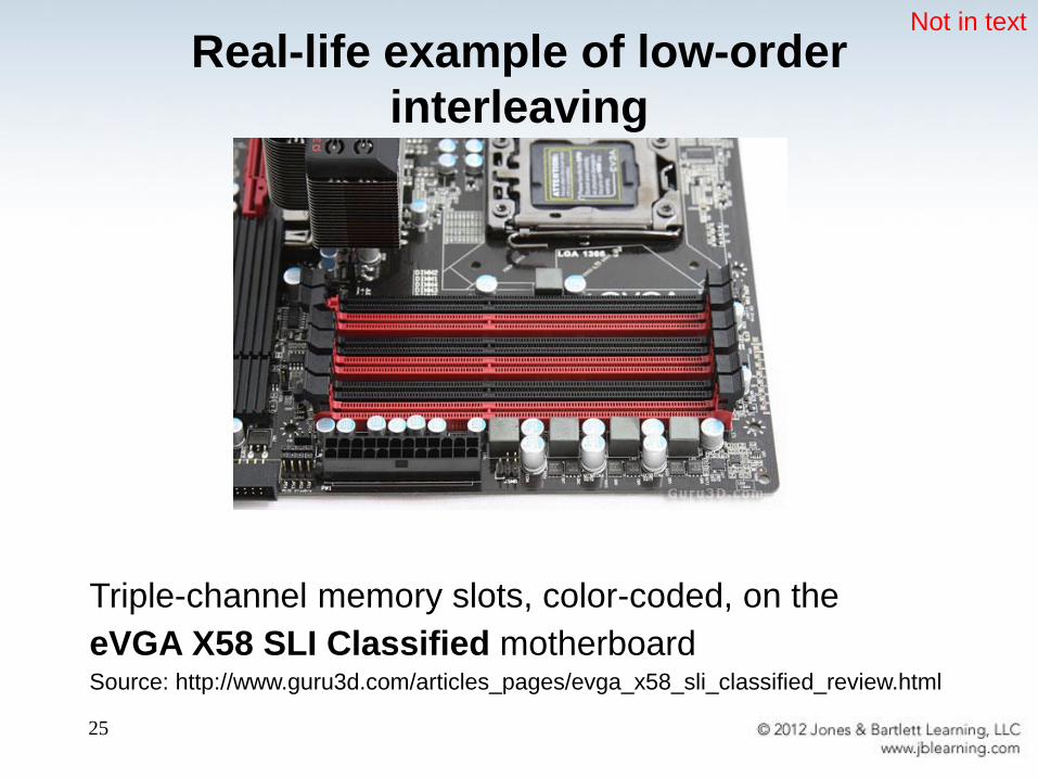
Real-life example of low-order
interleaving
25
Triple-channel memory slots, color-coded, on the
eVGA X58 SLI Classified motherboard Source: http://www.guru3d.com/articles_pages/evga_x58_sli_classified_review.html
Not in text
26
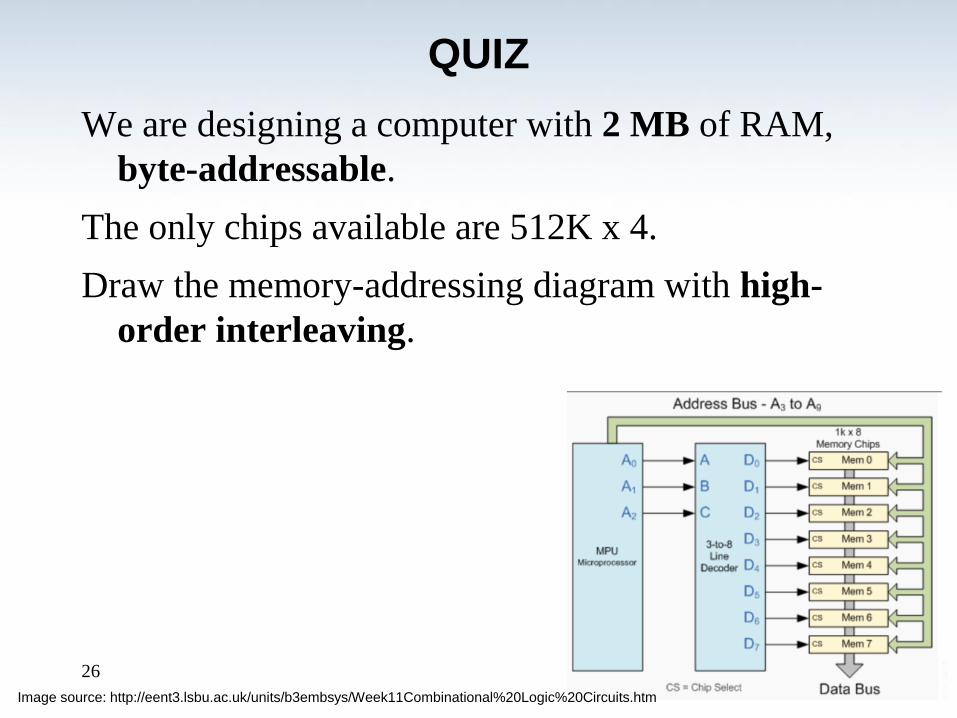
We are designing a computer with 2 MB of RAM,
byte-addressable.
The only chips available are 512K x 4.
Draw the memory-addressing diagram with high-
order interleaving.
QUIZ
Image source: http://eent3.lsbu.ac.uk/units/b3embsys/Week11Combinational%20Logic%20Circuits.htm
27
4.7 Interrupts
• The normal execution of a program is altered when
an event of higher-priority occurs. The CPU is
alerted to such an event through an interrupt.
• Interrupts can be triggered by:
– I/O requests
– Arithmetic errors (such as division by zero)
– Memory parity errors
– Invalid instruction
– User-defined breakpoints (debugging)
28
4.7 Interrupts
• Each interrupt is associated with an interrupt-
handling procedure that directs the actions of
the CPU when an interrupt occurs.
• Interrupts can be:
– Maskable → CPU can be instructed to ignore them
under certain circumstances
– Nonmaskable → High-priority interrupts that cannot
be ignored under any circumstances
29
4.8 MARIE
• Our model computer, the Machine Architecture that
is Really Intuitive and Easy, MARIE, was designed
for the singular purpose of illustrating basic computer
system concepts.
• While this system is too simple to do anything useful
in the real world, understanding of its functions will
enable us to comprehend system architectures that
are much more complex.
30
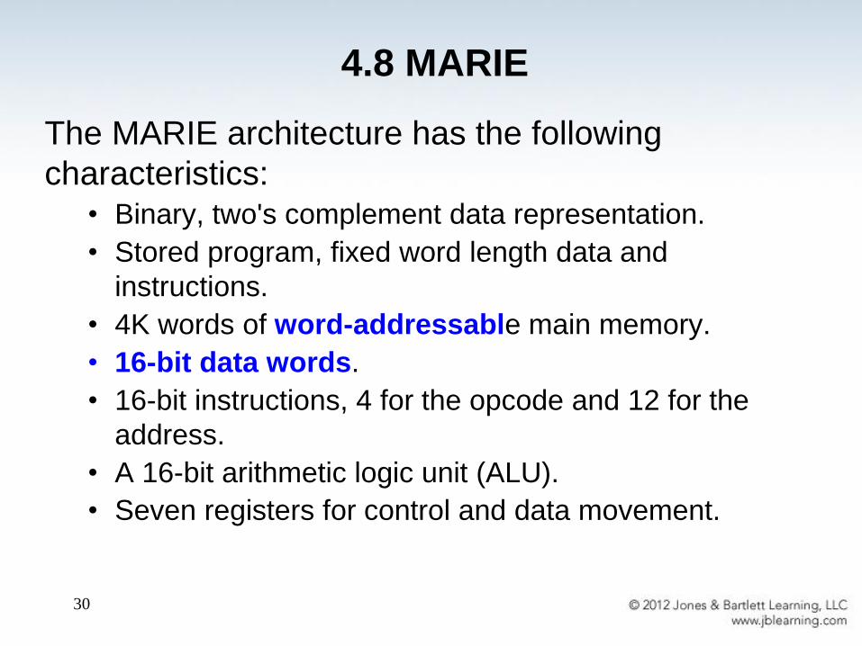
The MARIE architecture has the following
characteristics:• Binary, two's complement data representation.
• Stored program, fixed word length data and
instructions.
• 4K words of word-addressable main memory.
• 16-bit data words.
• 16-bit instructions, 4 for the opcode and 12 for the
address.
• A 16-bit arithmetic logic unit (ALU).
• Seven registers for control and data movement.
4.8 MARIE

31
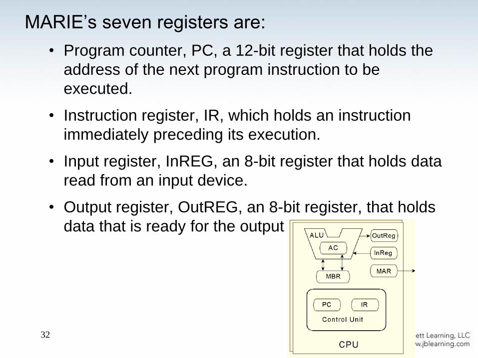
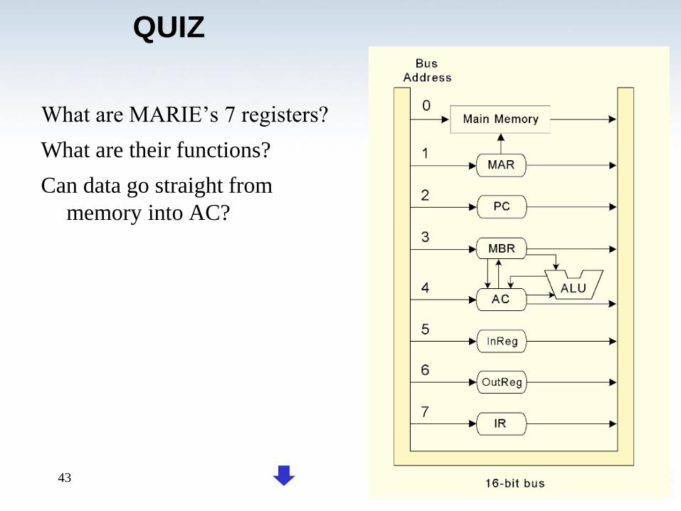
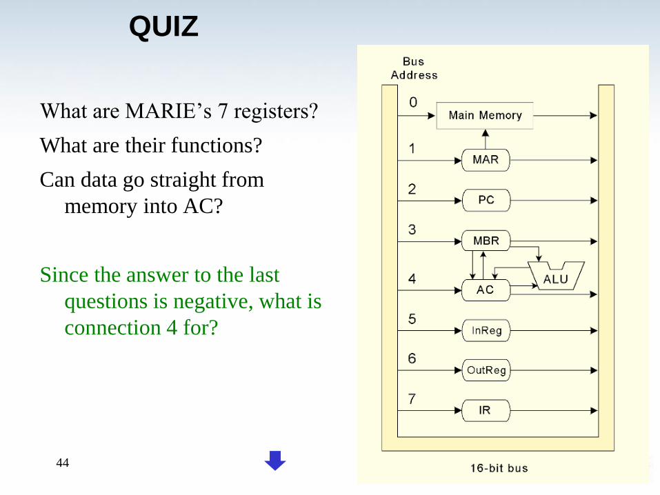
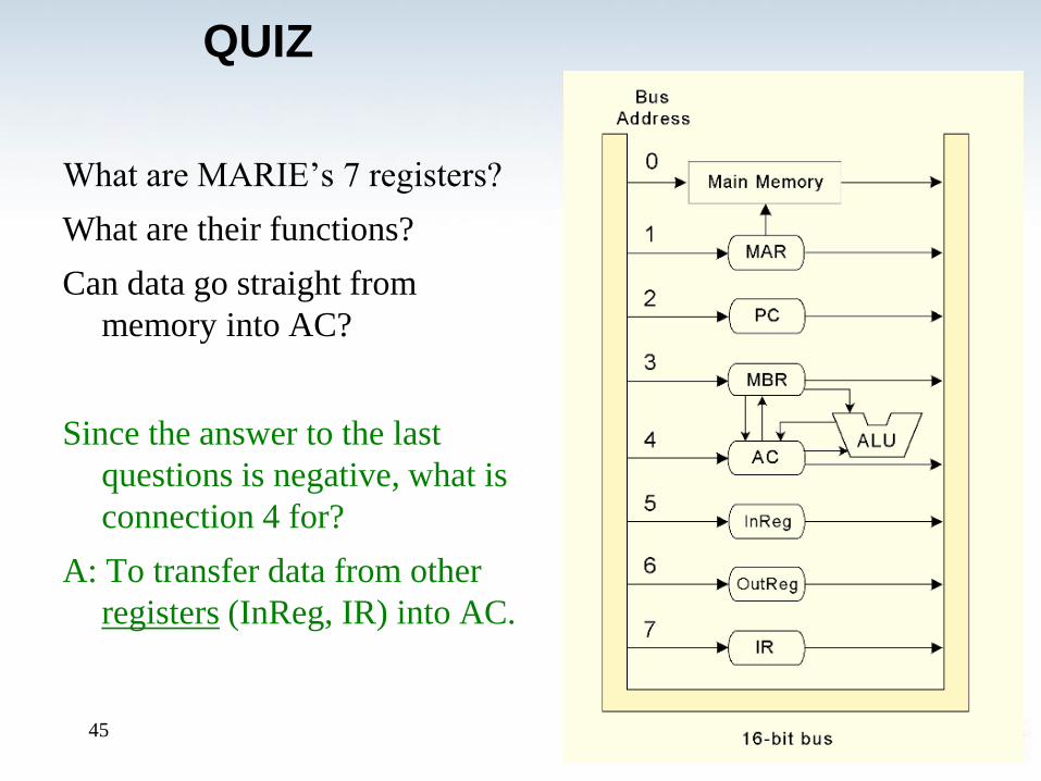
MARIE’s seven registers are:
• Accumulator, AC, a 16-bit register that holds an
operand:
• The one operand for a conditional operator (e.g., "less than")
• One of the two operands of a two-operand instruction.
• Memory address register, MAR, a 12-bit register that
holds the memory address of an instruction or the
operand of an instruction.
• Memory buffer register, MBR, a 16-bit register that
holds the data after its retrieval from, or before its
placement in memory.
32
MARIE’s seven registers are:
• Program counter, PC, a 12-bit register that holds the
address of the next program instruction to be
executed.
• Instruction register, IR, which holds an instruction
immediately preceding its execution.
• Input register, InREG, an 8-bit register that holds data
read from an input device.
• Output register, OutREG, an 8-bit register, that holds
data that is ready for the output device.
33
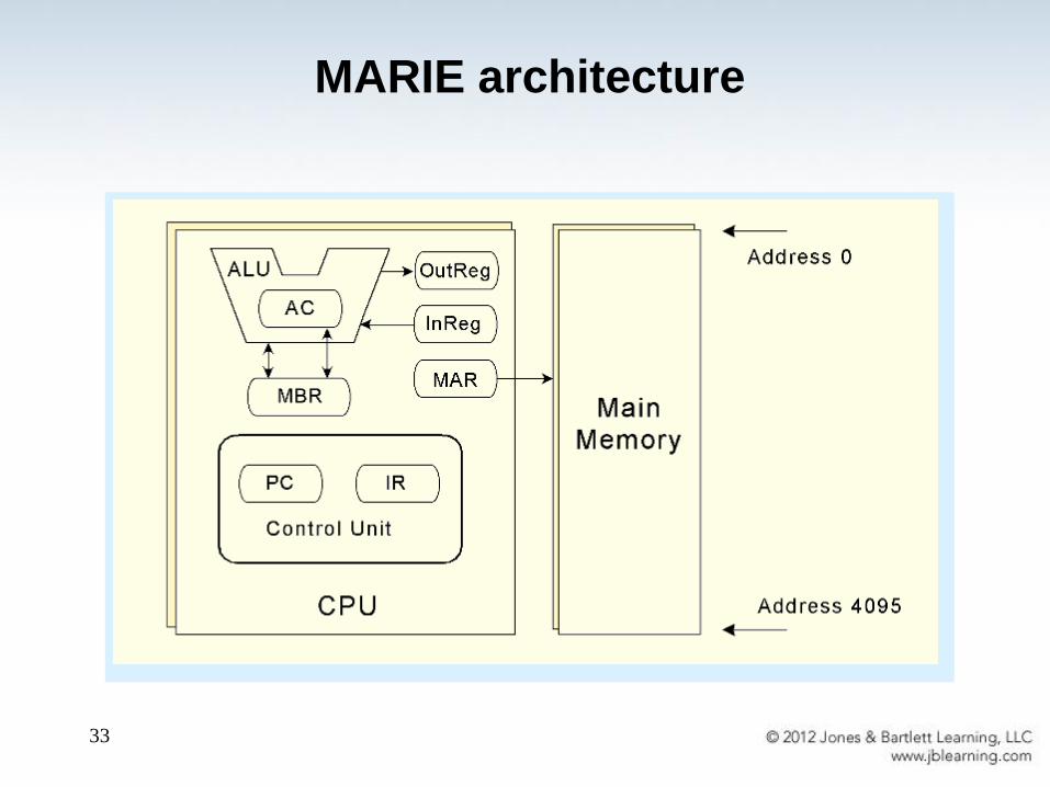
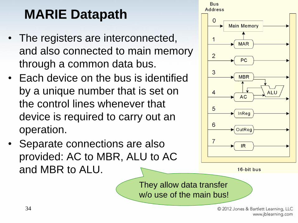
MARIE architecture
34
• The registers are interconnected,
and also connected to main memory
through a common data bus.
• Each device on the bus is identified
by a unique number that is set on
the control lines whenever that
device is required to carry out an
operation.
• Separate connections are also
provided: AC to MBR, ALU to AC
and MBR to ALU.
MARIE Datapath
They allow data transfer
w/o use of the main bus!
35
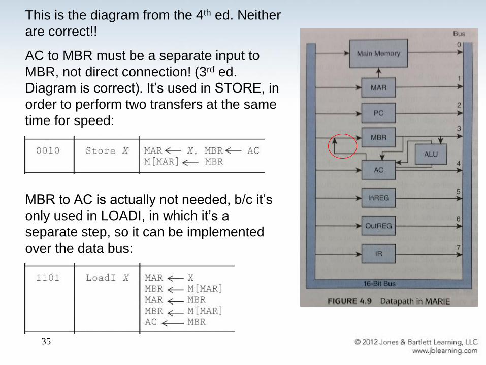
This is the diagram from the 4th ed. Neither
are correct!!
AC to MBR must be a separate input to
MBR, not direct connection! (3rd ed.
Diagram is correct). It’s used in STORE, in
order to perform two transfers at the same
time for speed:
MBR to AC is actually not needed, b/c it’s
only used in LOADI, in which it’s a
separate step, so it can be implemented
over the data bus:
36

To do for next time:
• Read pp.224-233 of Ch.4
• Answer Review Questions 16 through 25
• Solve Exercises 4, 7
37
EOL 1

QUIZ
Exercise 15
38
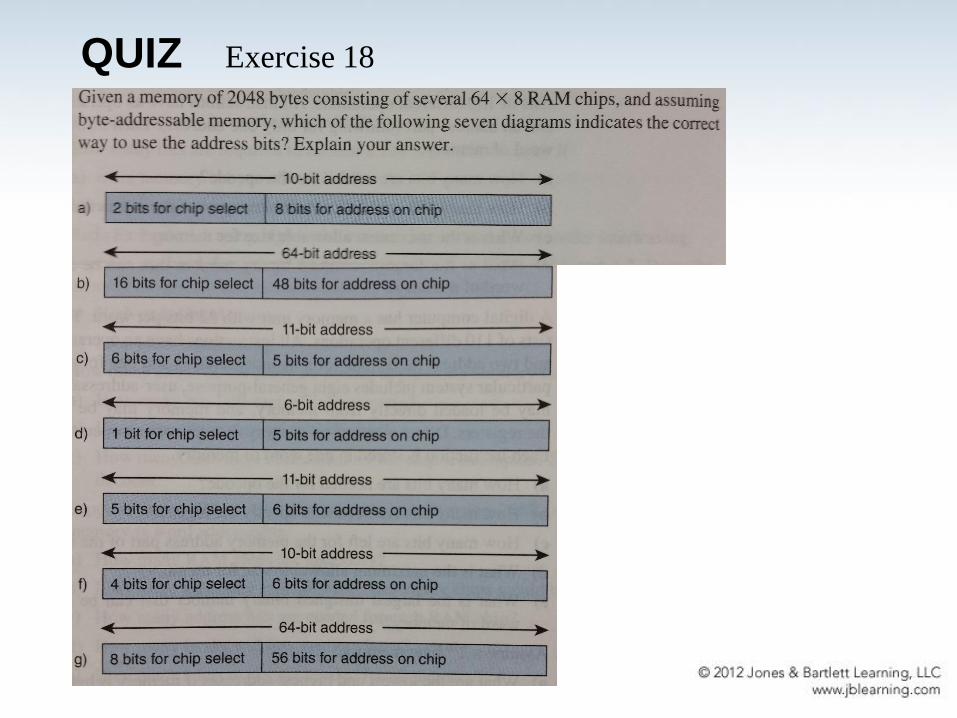
QUIZ Exercise 18
39

40
Why do high-performance computers use low-
order interleaving for their memory chips?
QUIZ

41
We are designing a computer with 2 MB of RAM,
byte-addressable.
The only chips available are 512K x 4.
Draw the memory-addressing diagram with high-
order interleaving.
QUIZ
Image source: http://eent3.lsbu.ac.uk/units/b3embsys/Week11Combinational%20Logic%20Circuits.htm
42
What are interrupts?
Why are they needed in the operation of a
computer?
QUIZ
43
What are MARIE’s 7 registers?
What are their functions?
Can data go straight from
memory into AC?
QUIZ
44
What are MARIE’s 7 registers?
What are their functions?
Can data go straight from
memory into AC?
Since the answer to the last
questions is negative, what is
connection 4 for?
QUIZ
45
What are MARIE’s 7 registers?
What are their functions?
Can data go straight from
memory into AC?
Since the answer to the last
questions is negative, what is
connection 4 for?
A: To transfer data from other
registers (InReg, IR) into AC.
QUIZ
46
• A computer’s instruction set architecture (ISA)
specifies the format of its instructions and the
primitive operations that the hardware can perform.
• The ISA is an interface between a computer’s
hardware and its software.
• The concept of an ISA was invented at IBM in the
1980s, for their System/360 family of computers (see
links on webpage).
4.8.3 MARIE ISA

47
• Some ISAs include hundreds of different instructions
for processing data and controlling program
execution.
• The MARIE ISA consists of only 13 “fundamental”
instructions.
• Real-life ISAs often have hundreds of instructions.
4.8.3 MARIE ISA
48
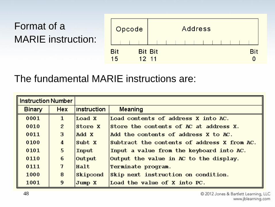
Format of a
MARIE instruction:
The fundamental MARIE instructions are:
49
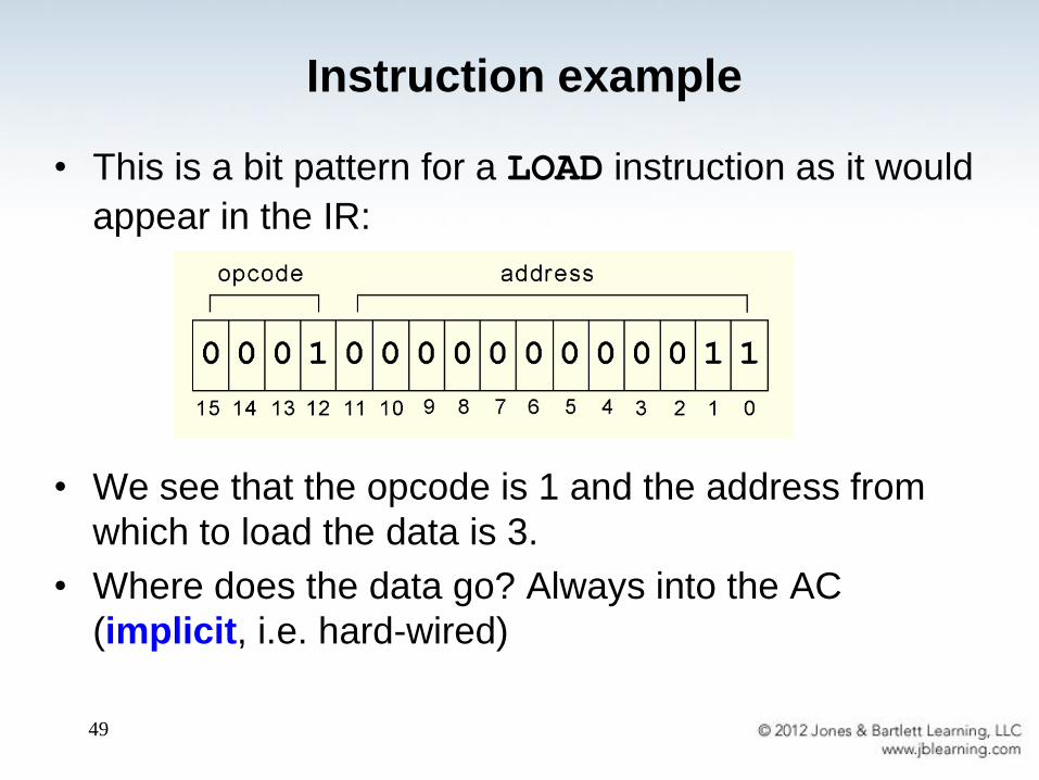
• This is a bit pattern for a LOAD instruction as it would
appear in the IR:
• We see that the opcode is 1 and the address from
which to load the data is 3.
• Where does the data go? Always into the AC
(implicit, i.e. hard-wired)
Instruction example
50
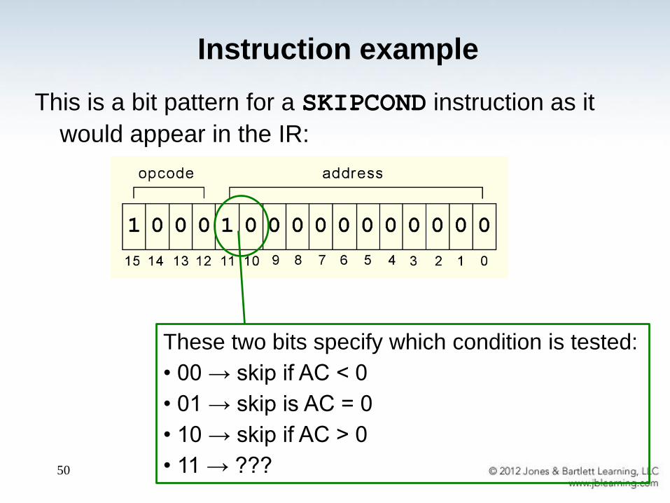
This is a bit pattern for a SKIPCOND instruction as it
would appear in the IR:
Instruction example
These two bits specify which condition is tested:
• 00 → skip if AC < 0
• 01 → skip is AC = 0
• 10 → skip if AC > 0
• 11 → ???
51
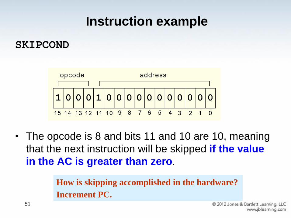
SKIPCOND
• The opcode is 8 and bits 11 and 10 are 10, meaning
that the next instruction will be skipped if the value
in the AC is greater than zero.
How is skipping accomplished in the hardware?
Increment PC.
Instruction example
52
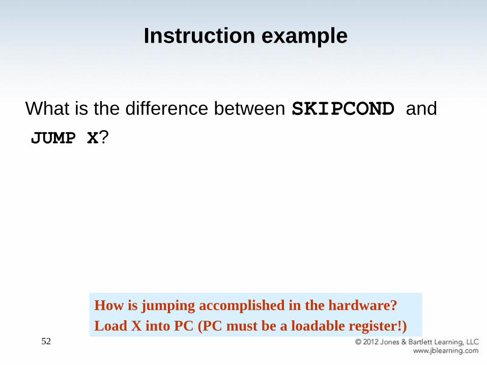
What is the difference between SKIPCOND and
JUMP X?
Instruction example
How is jumping accomplished in the hardware?
Load X into PC (PC must be a loadable register!)
53
• Each of our instructions actually consists of a
sequence of smaller instructions called
microoperations.
• The exact sequence of microoperations that are
carried out by an instruction can be specified using
register transfer language (RTL).
In the MARIE RTL, we use the notation M[X] to indicate
the actual data value stored in memory location X,
and to indicate the transfer of bytes to a register or
memory location.
Microops and RTL
54
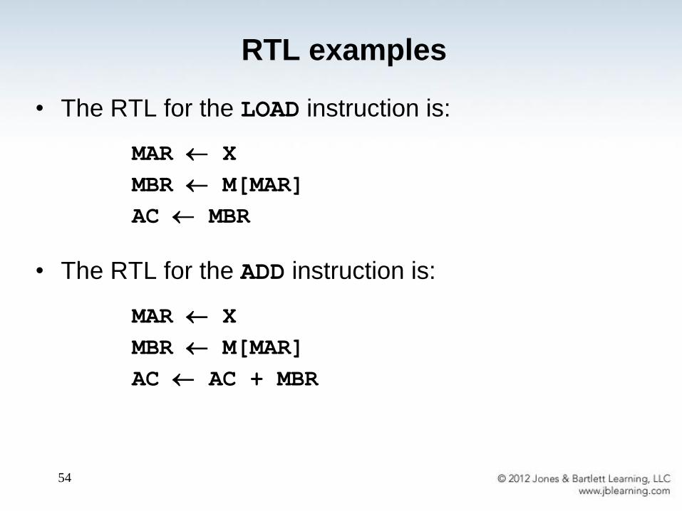
• The RTL for the LOAD instruction is:
• The RTL for the ADD instruction is:
MAR X
MBR M[MAR]
AC AC + MBR
MAR X
MBR M[MAR]
AC MBR
RTL examples
55
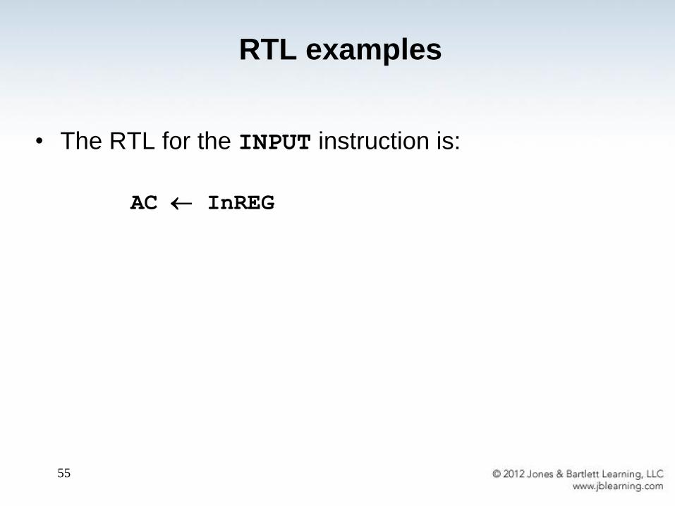
• The RTL for the INPUT instruction is:
AC InREG
RTL examples
56
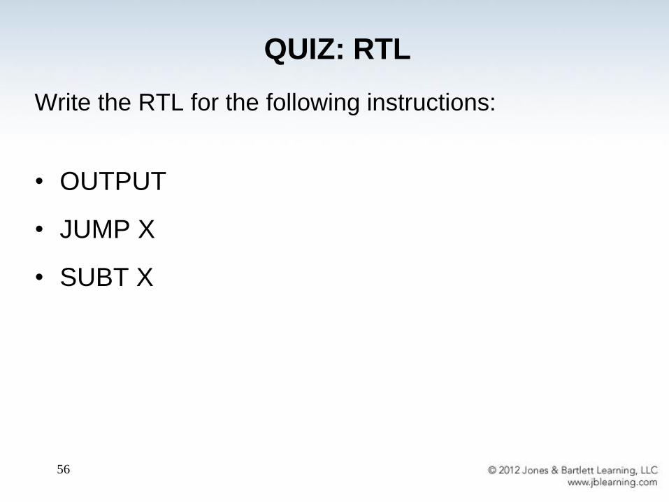
Write the RTL for the following instructions:
• OUTPUT
• JUMP X
• SUBT X
QUIZ: RTL
57
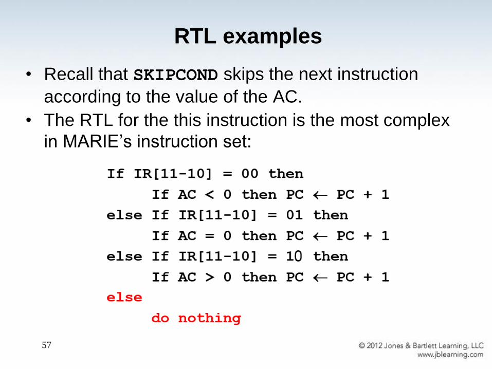
• Recall that SKIPCOND skips the next instruction
according to the value of the AC.
• The RTL for the this instruction is the most complex
in MARIE’s instruction set:
RTL examples
58
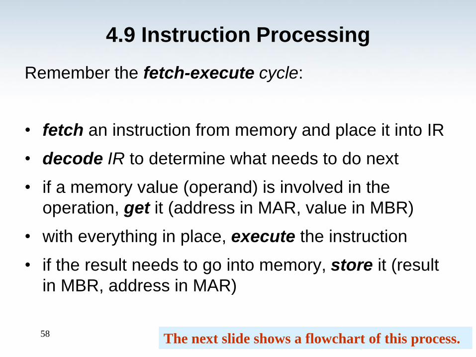
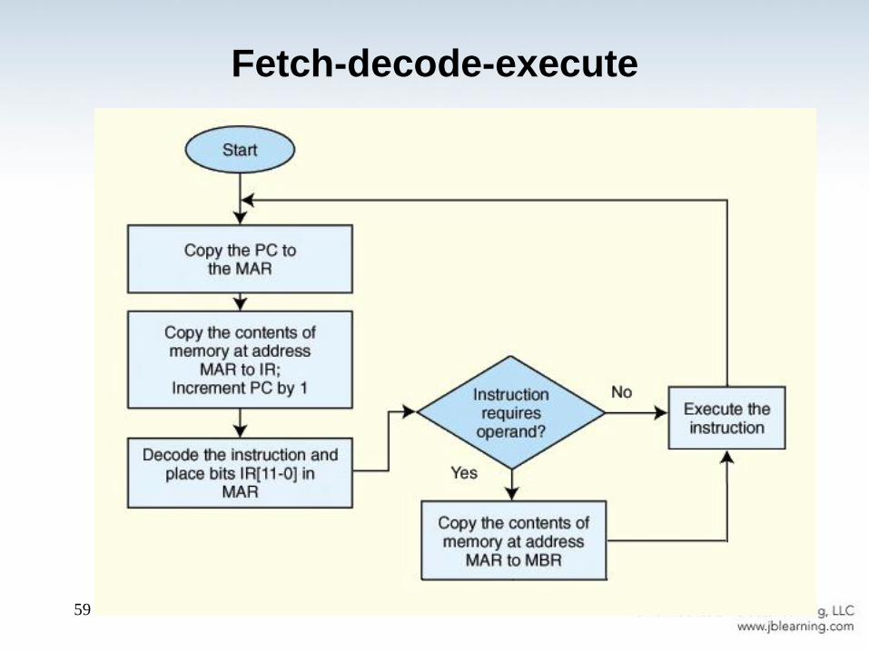
4.9 Instruction Processing
Remember the fetch-execute cycle:
• fetch an instruction from memory and place it into IR
• decode IR to determine what needs to do next
• if a memory value (operand) is involved in the
operation, get it (address in MAR, value in MBR)
• with everything in place, execute the instruction
• if the result needs to go into memory, store it (result
in MBR, address in MAR)
The next slide shows a flowchart of this process.
59
Fetch-decode-execute
60
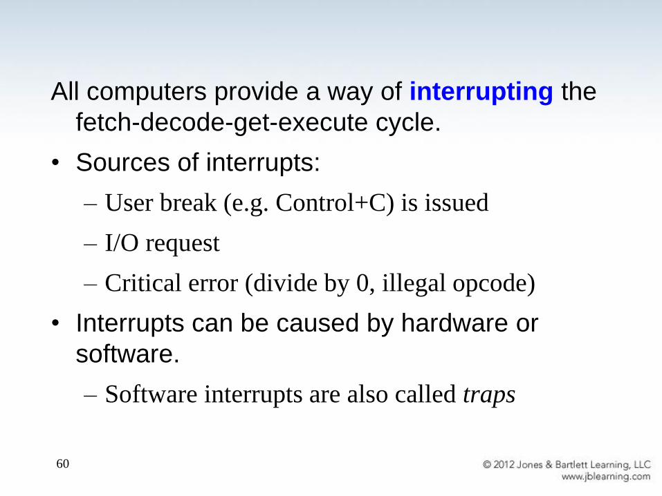
All computers provide a way of interrupting the
fetch-decode-get-execute cycle.
• Sources of interrupts:
– User break (e.g. Control+C) is issued
– I/O request
– Critical error (divide by 0, illegal opcode)
• Interrupts can be caused by hardware or
software.
– Software interrupts are also called traps
61
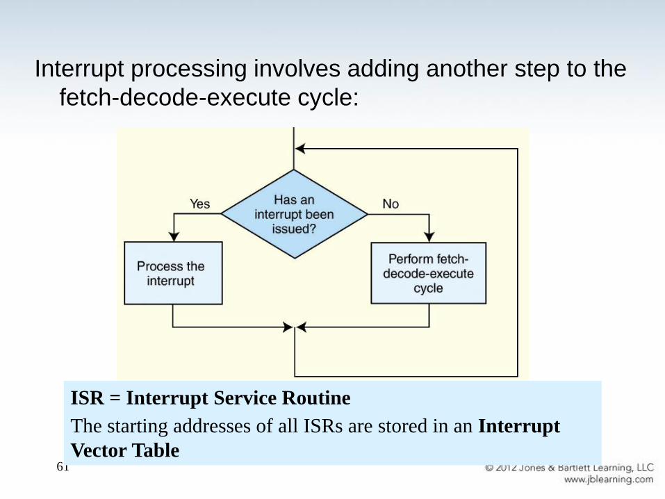
Interrupt processing involves adding another step to the
fetch-decode-execute cycle:
ISR = Interrupt Service Routine
The starting addresses of all ISRs are stored in an Interrupt
Vector Table
62
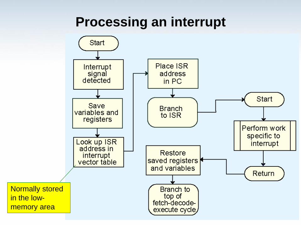
Processing an interrupt
Normally stored
in the low-
memory area
63
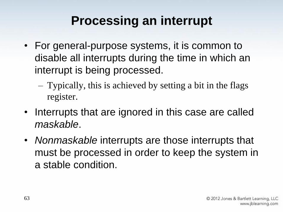
• For general-purpose systems, it is common to
disable all interrupts during the time in which an
interrupt is being processed.
– Typically, this is achieved by setting a bit in the flags
register.
• Interrupts that are ignored in this case are called
maskable.
• Nonmaskable interrupts are those interrupts that
must be processed in order to keep the system in
a stable condition.
Processing an interrupt
64
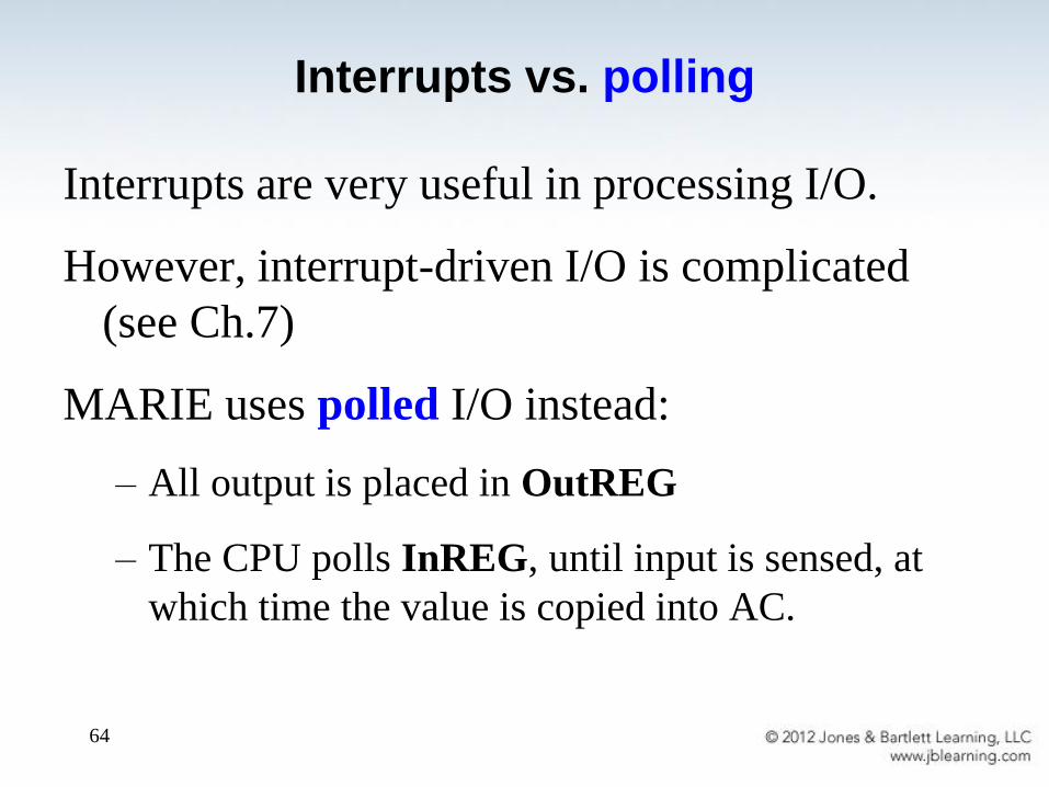
Interrupts are very useful in processing I/O.
However, interrupt-driven I/O is complicated
(see Ch.7)
MARIE uses polled I/O instead:
– All output is placed in OutREG
– The CPU polls InREG, until input is sensed, at
which time the value is copied into AC.
Interrupts vs. polling
65
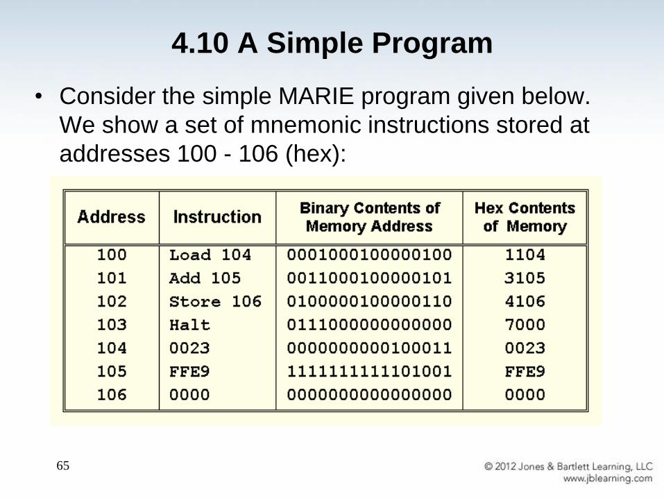
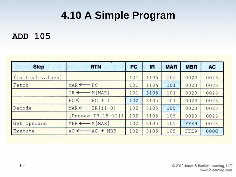
• Consider the simple MARIE program given below.
We show a set of mnemonic instructions stored at
addresses 100 - 106 (hex):
4.10 A Simple Program
66
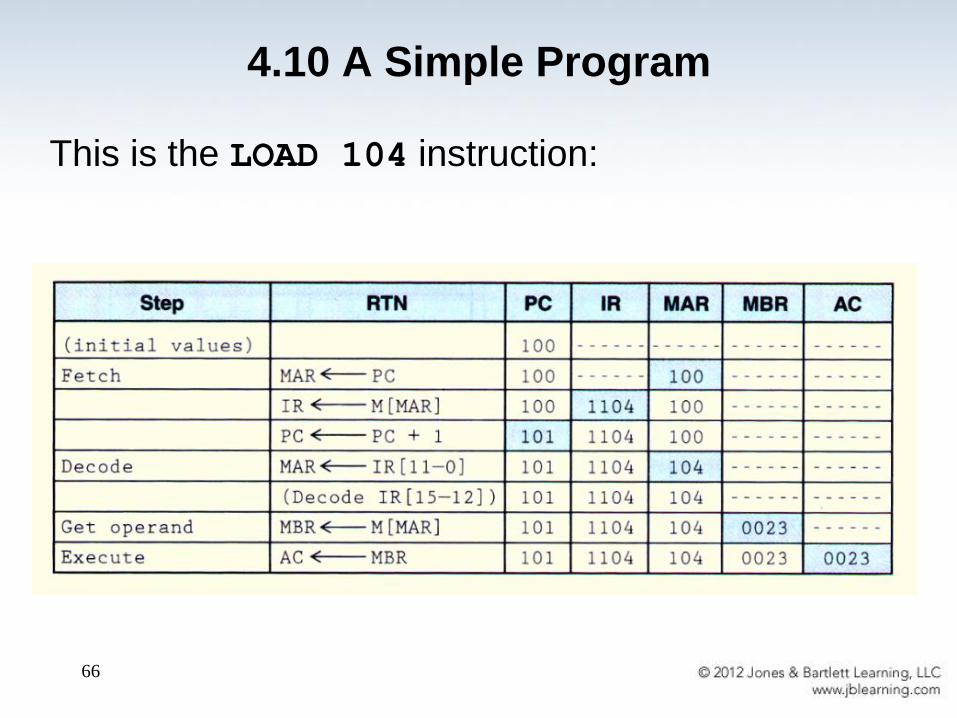
This is the LOAD 104 instruction:
4.10 A Simple Program
67
ADD 105
4.10 A Simple Program
68
4.11 Discussion on Assemblers
Assemblers translate mnemonics (instructions that are
comprehensible to humans) into the machine
language that is comprehensible to computers
Distinction between an assembler and a compiler:
• In assembly language, there is a one-to-one
correspondence between a mnemonic instruction and
its machine code.
• With compilers, this is not usually the case.
69
• Assemblers create an object program file from
mnemonic source code in two passes.
• During the first pass, the assembler assembles as
much of the program as it can, while it builds a
symbol table that contains memory references for
all symbols in the program.
• During the second pass, the instructions are
completed using the values from the symbol table.
4.11 Assemblers
70
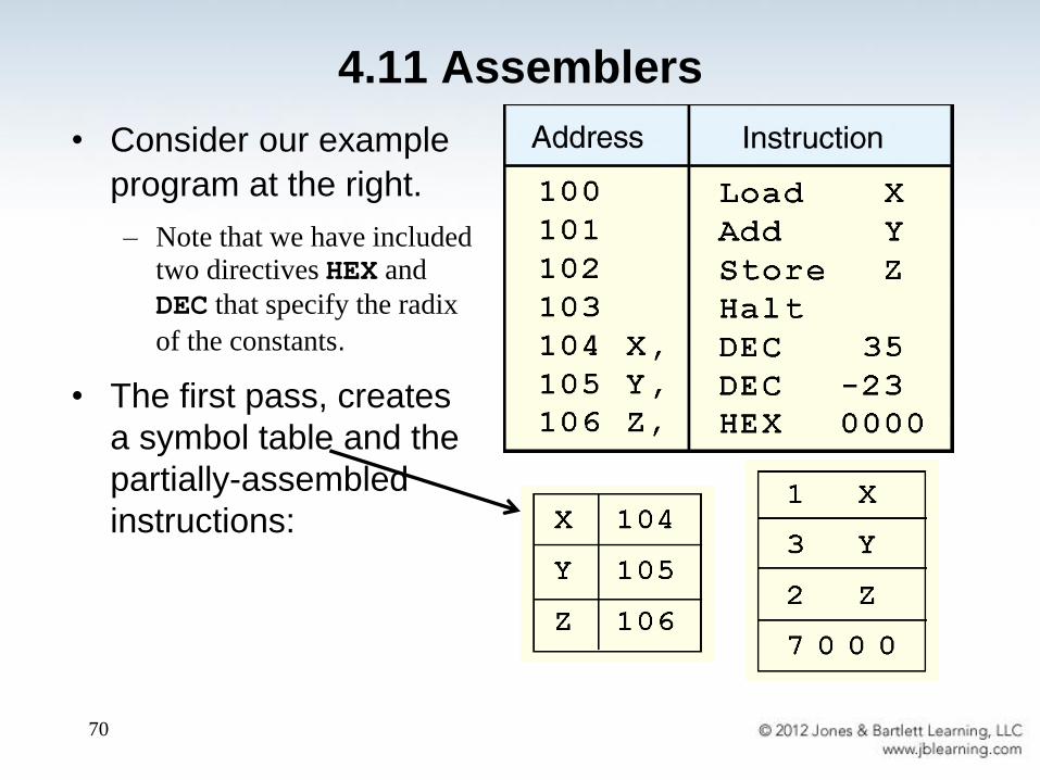
• Consider our example
program at the right.
– Note that we have included two directives HEX and
DEC that specify the radix
of the constants.
• The first pass, creates
a symbol table and the
partially-assembled
instructions:
4.11 Assemblers

71
• After the second pass, the
assembly is complete.
4.11 Assemblers
72
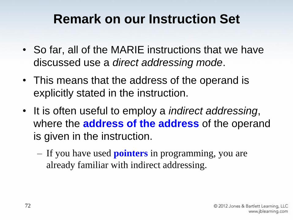
Remark on our Instruction Set
• So far, all of the MARIE instructions that we have
discussed use a direct addressing mode.
• This means that the address of the operand is
explicitly stated in the instruction.
• It is often useful to employ a indirect addressing,
where the address of the address of the operand
is given in the instruction.
– If you have used pointers in programming, you are
already familiar with indirect addressing.

Individual work recommended:
3, 5, 6
73
EOL 2
74
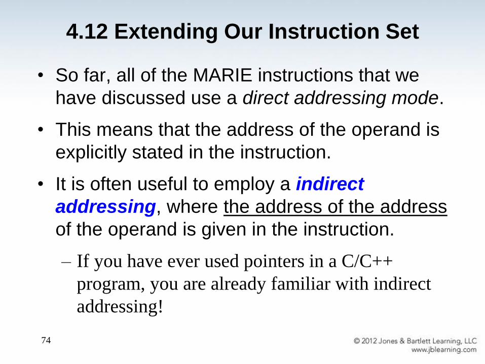
4.12 Extending Our Instruction Set
• So far, all of the MARIE instructions that we
have discussed use a direct addressing mode.
• This means that the address of the operand is
explicitly stated in the instruction.
• It is often useful to employ a indirect
addressing, where the address of the address
of the operand is given in the instruction.
– If you have ever used pointers in a C/C++
program, you are already familiar with indirect
addressing!
75
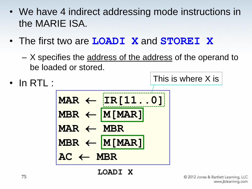
• We have 4 indirect addressing mode instructions in
the MARIE ISA.
• The first two are LOADI X and STOREI X
– X specifies the address of the address of the operand to
be loaded or stored.
• In RTL :
MAR IR[11..0]
MBR M[MAR]
MAR MBR
MBR M[MAR]
AC MBR
LOADI X
This is where X is
76
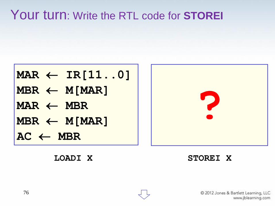
Your turn: Write the RTL code for STOREI
MAR IR[11..0]
MBR M[MAR]
MAR MBR
MBR M[MAR]
AC MBR
?STOREI XLOADI X
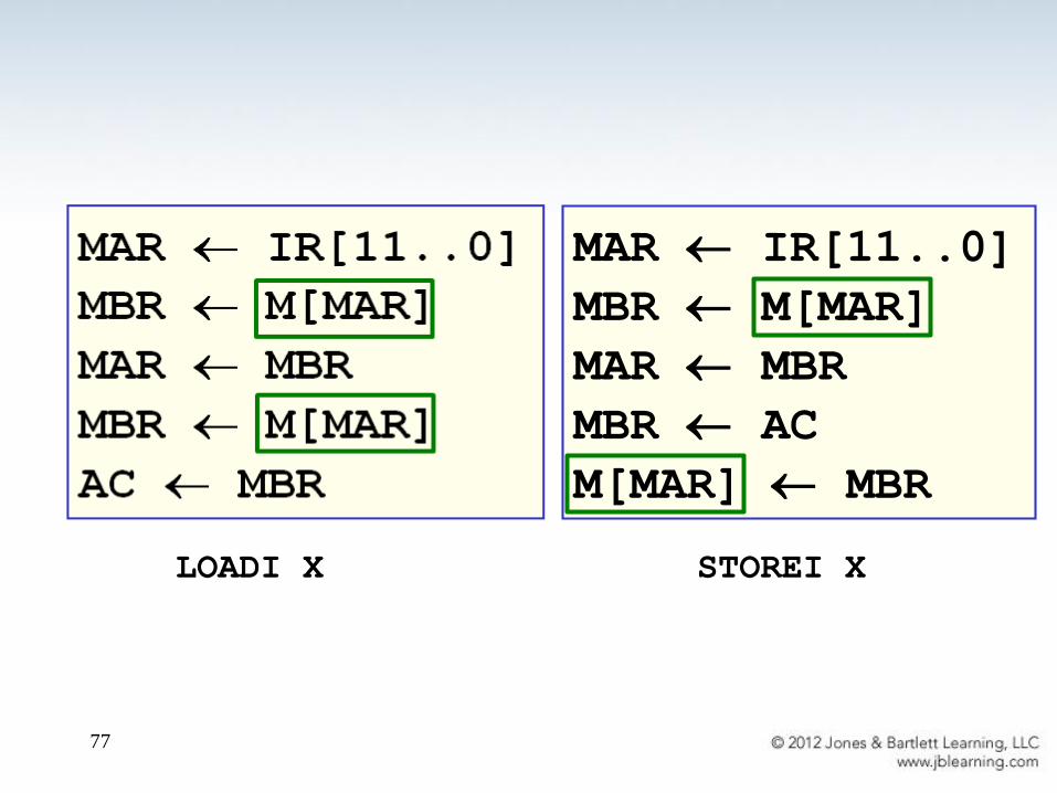
77
MAR IR[11..0]
MBR M[MAR]
MAR MBR
MBR AC
M[MAR] MBR
STOREI XLOADI X
78
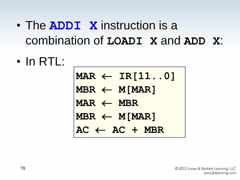
• The ADDI X instruction is a
combination of LOADI X and ADD X:
• In RTL: MAR IR[11..0]
MBR M[MAR]
MAR MBR
MBR M[MAR]
AC AC + MBR
79
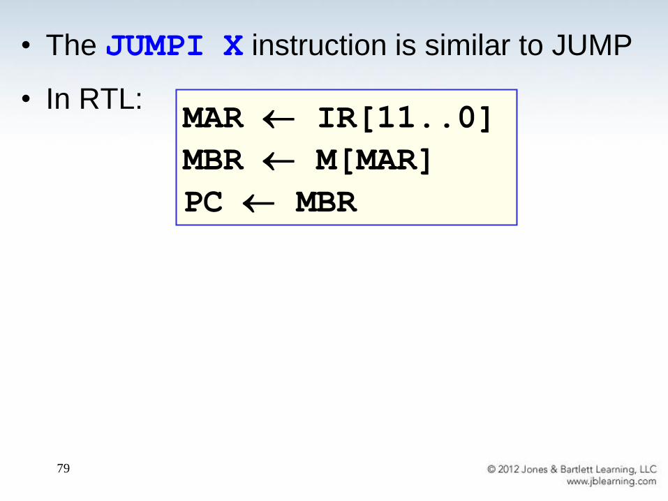
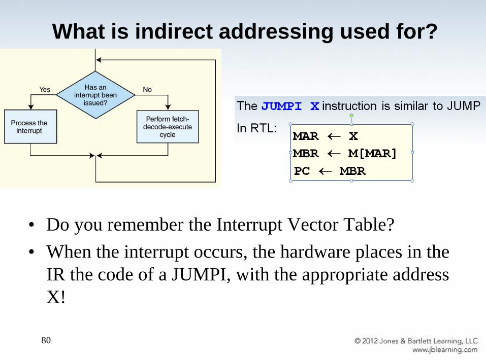
• The JUMPI X instruction is similar to JUMP
• In RTL: MAR IR[11..0]
MBR M[MAR]
PC MBR
80
What is indirect addressing used for?
• Do you remember the Interrupt Vector Table?
• When the interrupt occurs, the hardware places in the
IR the code of a JUMPI, with the appropriate address
X!

Extra-credit
81
82
100 | LOAD Addr
101 | STORE Next
102 | LOAD Num
103 | SUBT One
104 | STORE Ctr
105 |Loop LOAD Sum
106 | ADDI Next
107 | STORE Sum
108 | LOAD Next
109 | ADD One
10A | STORE Next
10B | LOAD Ctr
10C | SUBT One
10D | STORE Ctr
10E | SKIPCOND 000
10F | JUMP Loop
110 | HALT
111 |Addr HEX 117
112 |Next HEX 0
113 |Num DEC 5
114 |Sum DEC 0
115 |Ctr HEX 0
116 |One DEC 1
117 | DEC 10
118 | DEC 15
119 | DEC 2
11A | DEC 25
11B | DEC 30
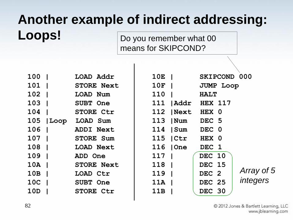
Another example of indirect addressing:
Loops! Do you remember what 00
means for SKIPCOND?
Array of 5
integers
83
100 | LOAD Addr
101 | STORE Next
102 | LOAD Num
103 | SUBT One
104 | STORE Ctr
105 |Loop LOAD Sum
106 | ADDI Next
107 | STORE Sum
108 | LOAD Next
109 | ADD One
10A | STORE Next
10B | LOAD Ctr
10C | SUBT One
10D | STORE Ctr
10E | SKIPCOND 000
10F | JUMP Loop
110 | HALT
111 |Addr HEX 117
112 |Next HEX 0
113 |Num DEC 5
114 |Sum DEC 0
115 |Ctr HEX 0
116 |One DEC 1
117 | DEC 10
118 | DEC 15
119 | DEC 2
11A | DEC 25
11B | DEC 30
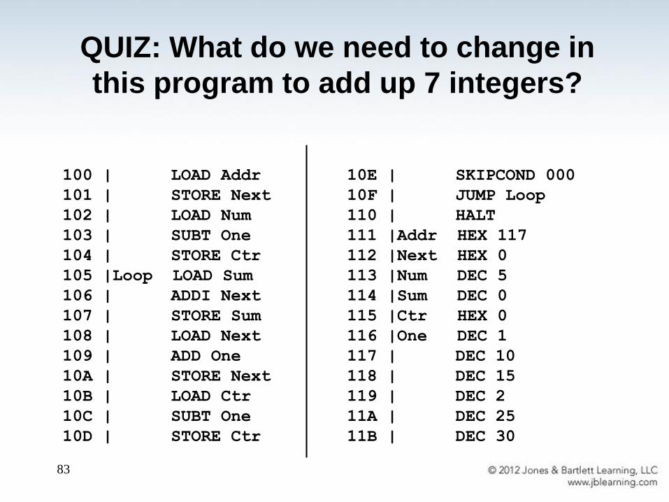
QUIZ: What do we need to change in
this program to add up 7 integers?
84
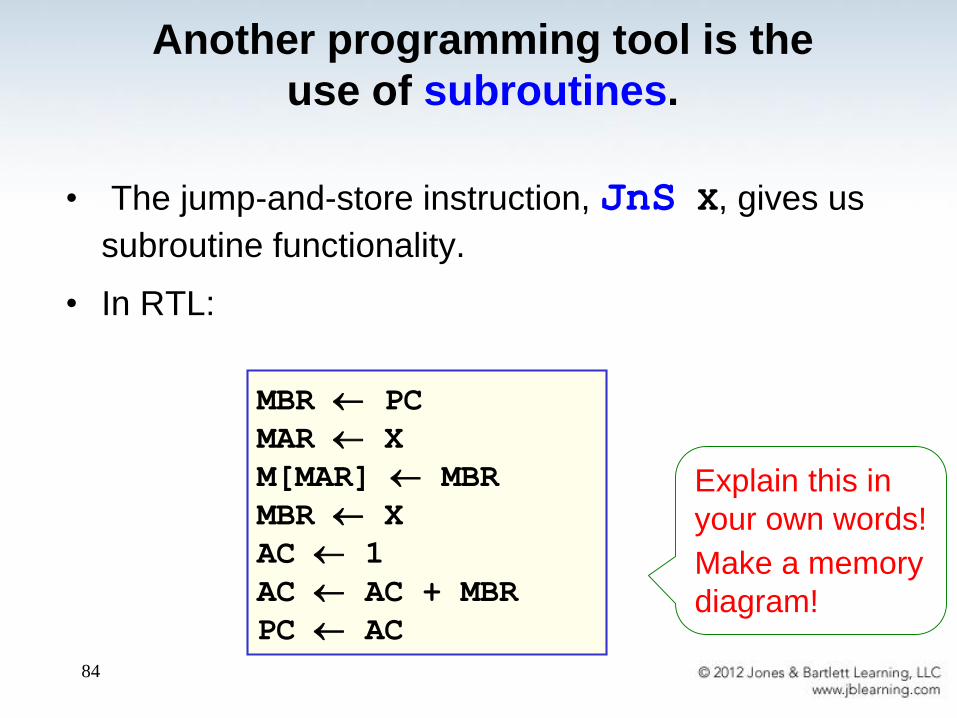
• The jump-and-store instruction, JnS X, gives us
subroutine functionality.
• In RTL:
MBR PC
MAR X
M[MAR] MBR
MBR X
AC 1
AC AC + MBR
PC AC
Another programming tool is the
use of subroutines.
Explain this in
your own words!
Make a memory
diagram!
85
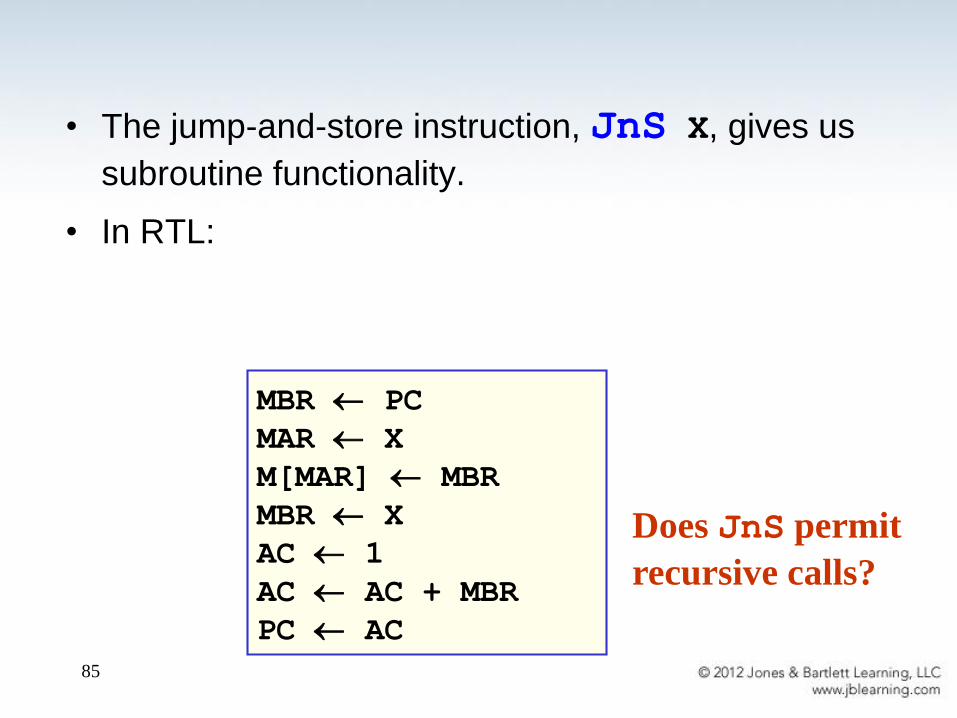
• The jump-and-store instruction, JnS X, gives us
subroutine functionality.
• In RTL:
MBR PC
MAR X
M[MAR] MBR
MBR X
AC 1
AC AC + MBR
PC AC
Does JnS permit
recursive calls?
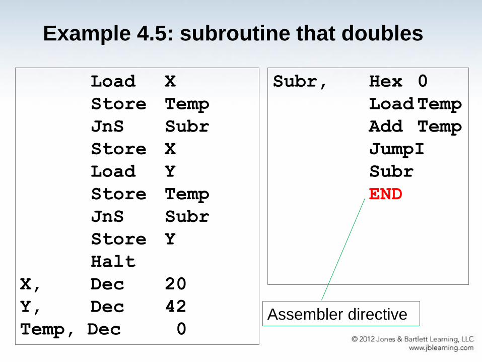
Example 4.5: subroutine that doubles
Load X
Store Temp
JnS Subr
Store X
Load Y
Store Temp
JnS Subr
Store Y
Halt
X, Dec 20
Y, Dec 42
Temp, Dec 0
Subr, Hex 0
LoadTemp
Add Temp
JumpI
Subr
END
Assembler directive
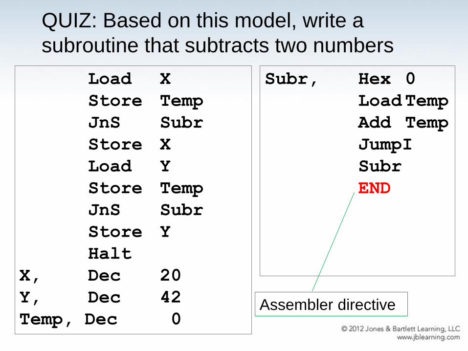
QUIZ: Based on this model, write a
subroutine that subtracts two numbers
Load X
Store Temp
JnS Subr
Store X
Load Y
Store Temp
JnS Subr
Store Y
Halt
X, Dec 20
Y, Dec 42
Temp, Dec 0
Subr, Hex 0
LoadTemp
Add Temp
JumpI
Subr
END
Assembler directive
88
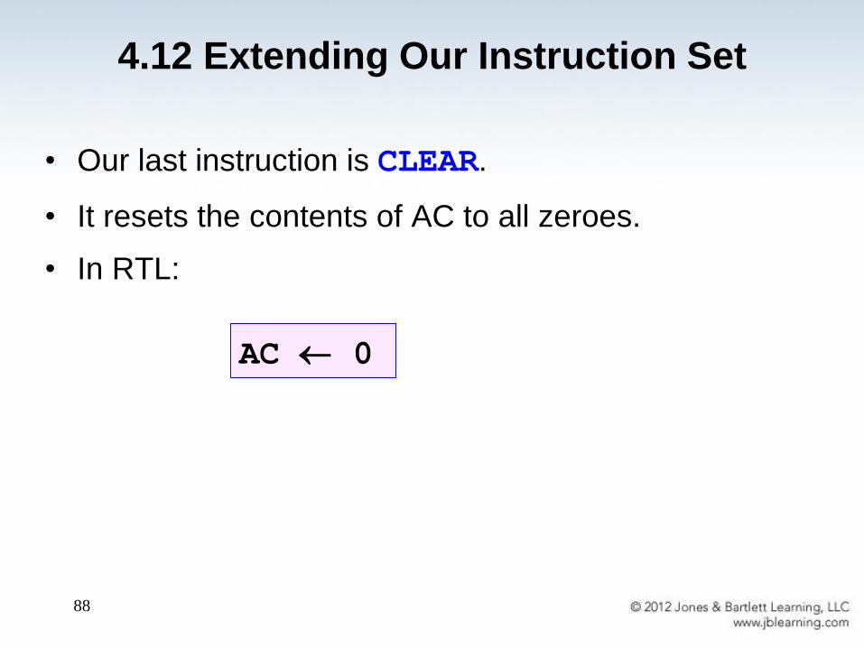
• Our last instruction is CLEAR.
• It resets the contents of AC to all zeroes.
• In RTL:
AC 0
4.12 Extending Our Instruction Set
89
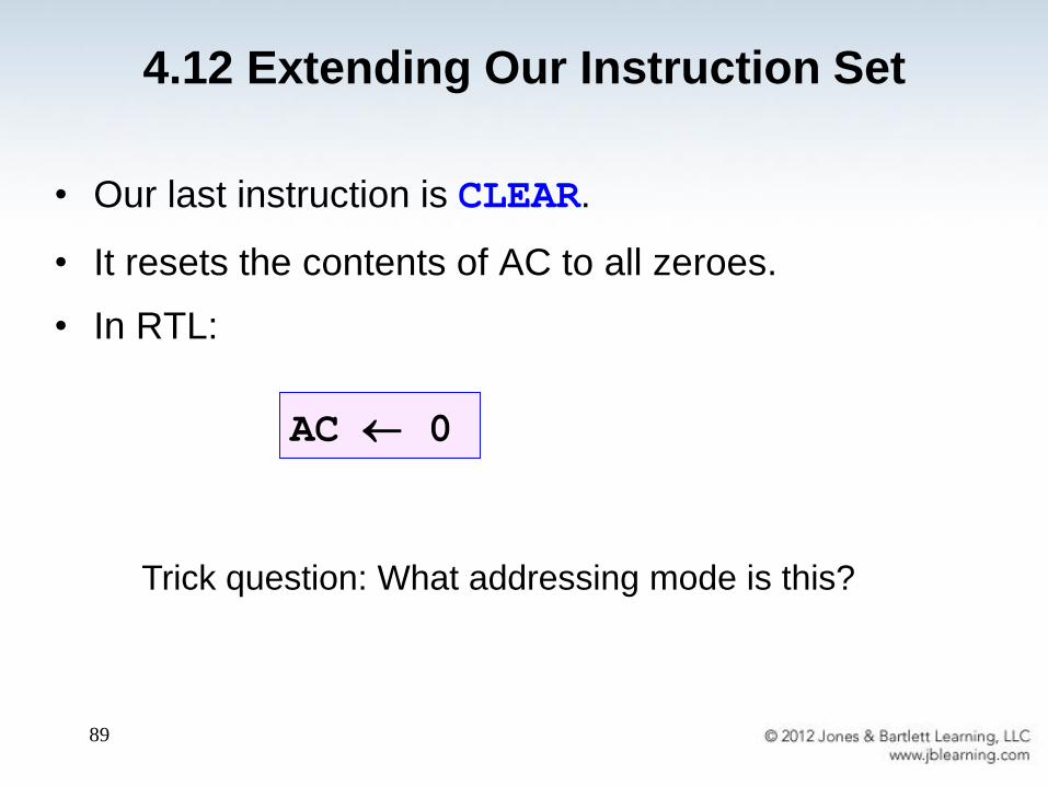
• Our last instruction is CLEAR.
• It resets the contents of AC to all zeroes.
• In RTL:
AC 0
4.12 Extending Our Instruction Set
Trick question: What addressing mode is this?

The new instructions
90
91
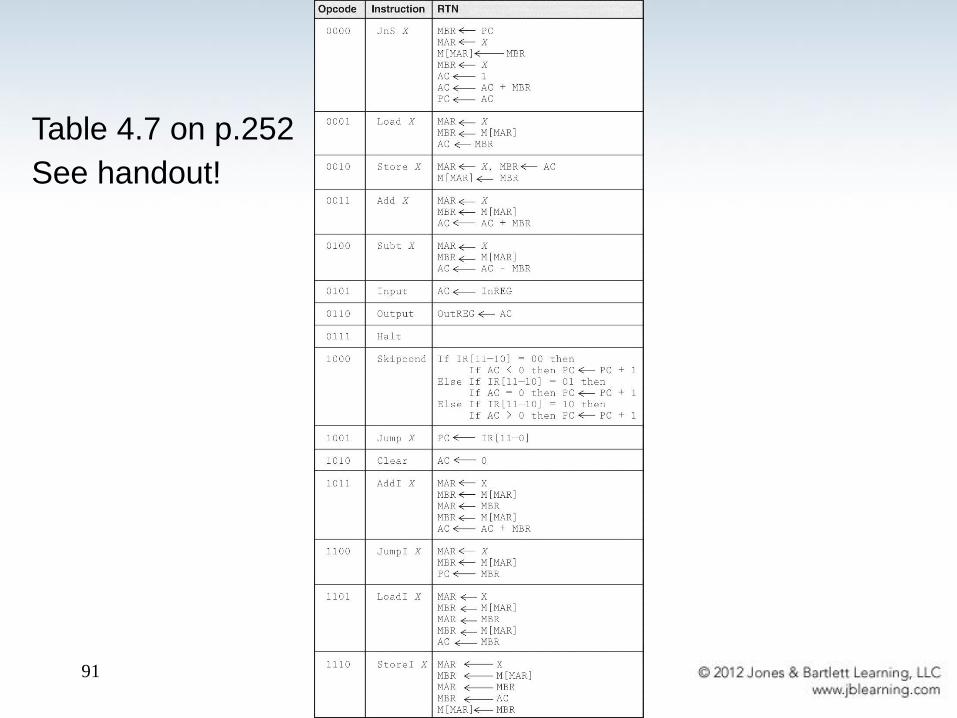
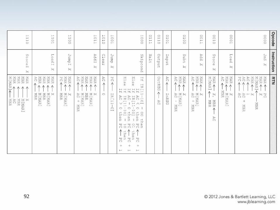
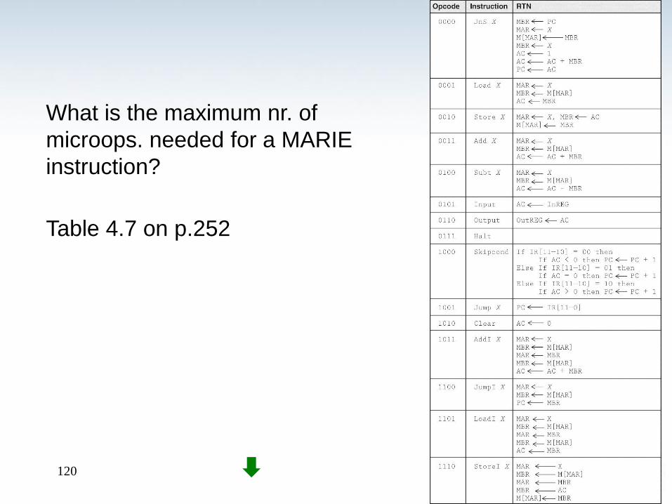
Table 4.7 on p.252
See handout!
92
93
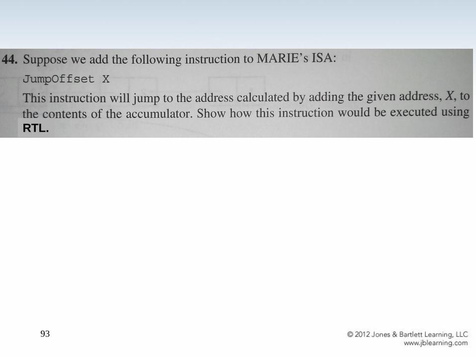
RTL.
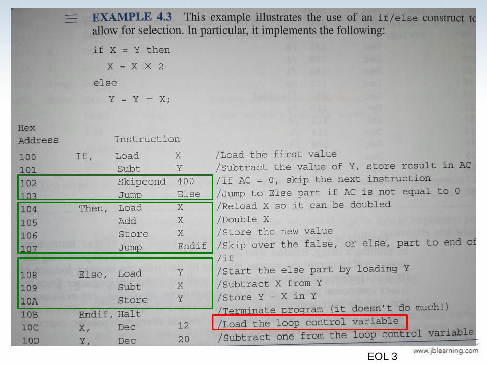
Implementing loops in assembly
94
EOL 3

Discussion of exam problems
95

QUIZ:
How/where do MARIE subroutines preserve
the return address?
96

QUIZ:
How/where do MARIE subroutines preserve
the return address?
97
QUIZ:
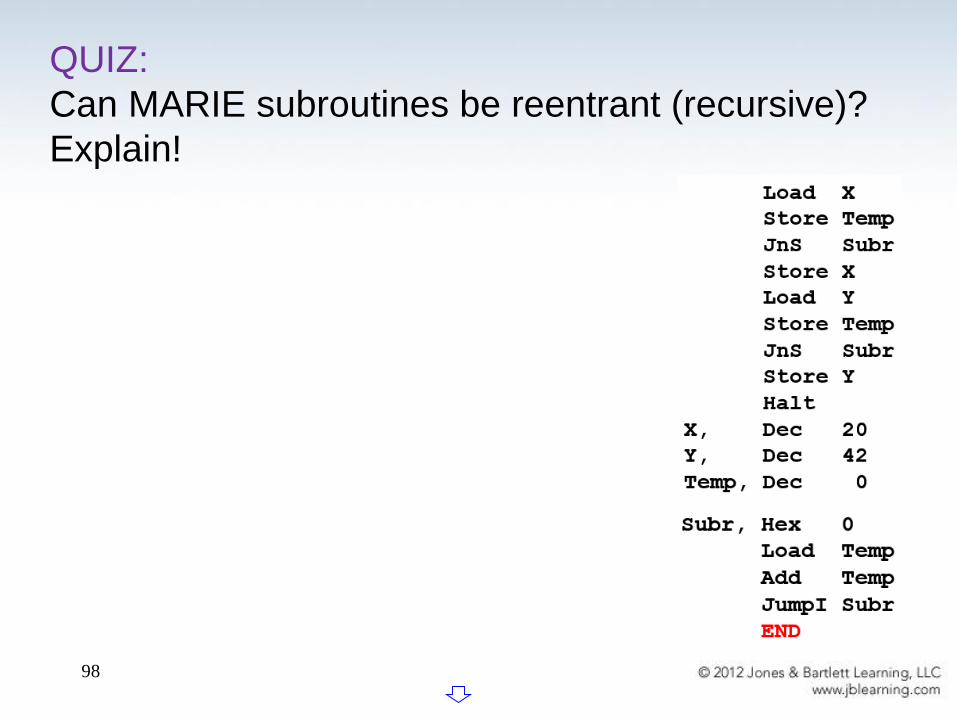
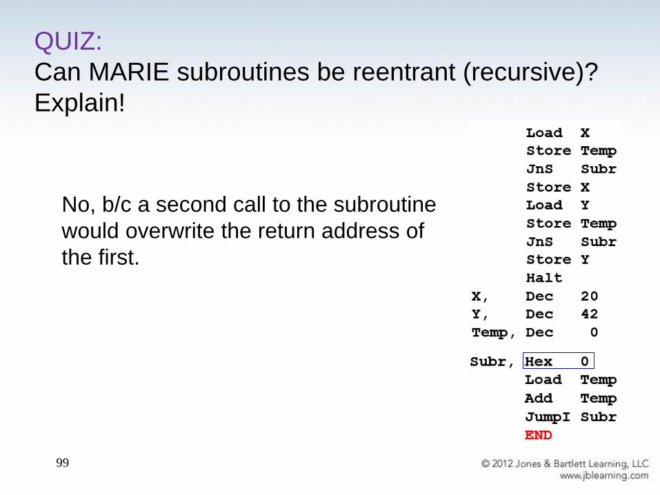
Can MARIE subroutines be reentrant (recursive)?
Explain!
98
QUIZ:
Can MARIE subroutines be reentrant (recursive)?
Explain!
99
No, b/c a second call to the subroutine
would overwrite the return address of
the first.
QUIZ:
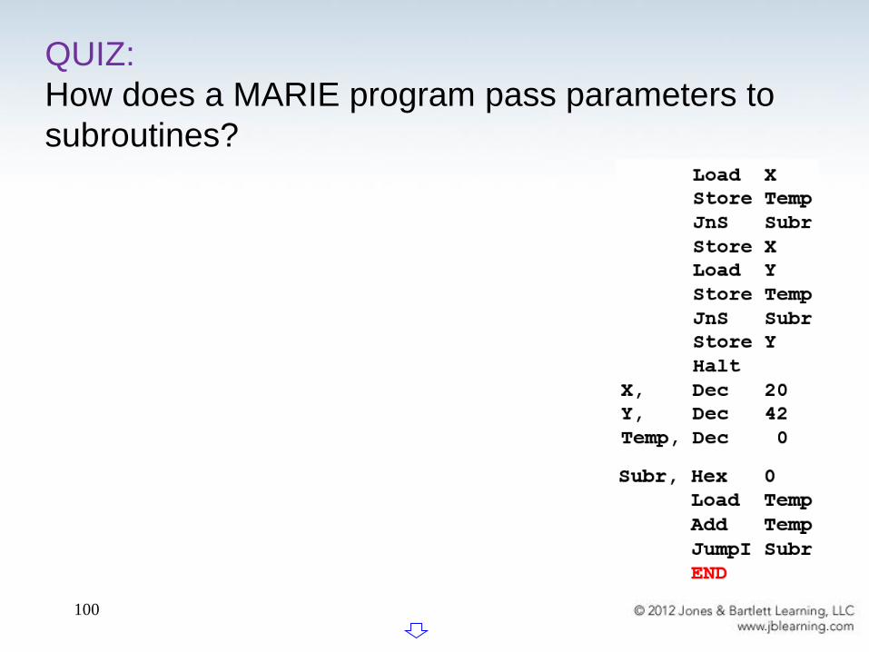
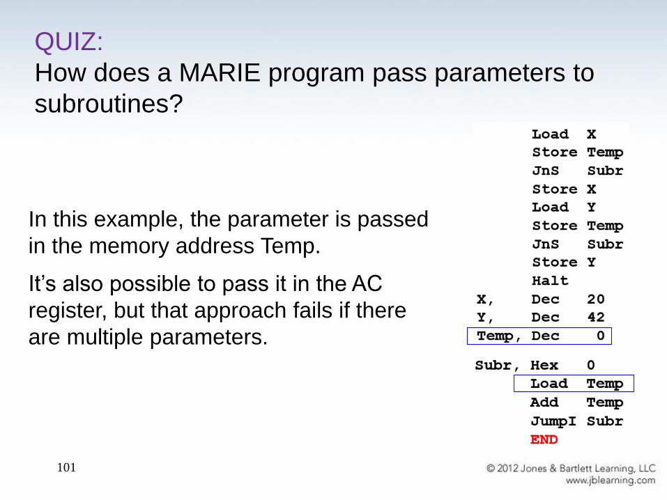
How does a MARIE program pass parameters to
subroutines?
100
QUIZ:
How does a MARIE program pass parameters to
subroutines?
101
In this example, the parameter is passed
in the memory address Temp.
It’s also possible to pass it in the AC
register, but that approach fails if there
are multiple parameters.

QUIZ:
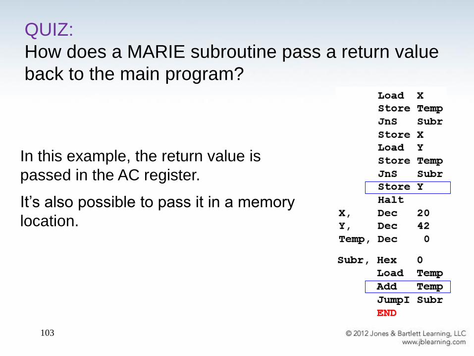
How does a MARIE subroutine pass a return value
back to the main program?
102
QUIZ:
How does a MARIE subroutine pass a return value
back to the main program?
103
In this example, the return value is
passed in the AC register.
It’s also possible to pass it in a memory
location.
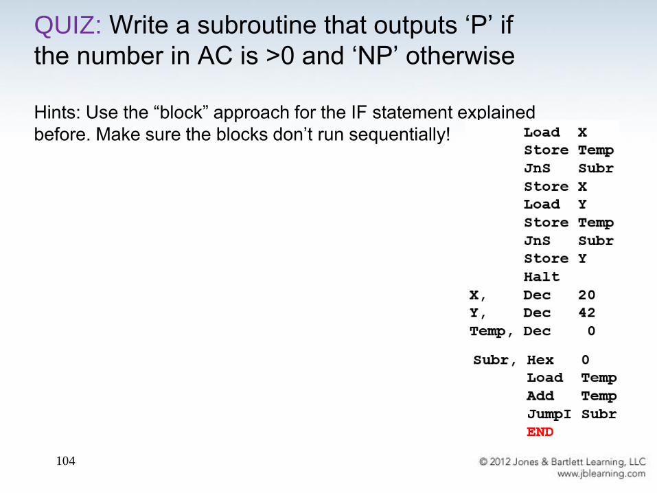
QUIZ: Write a subroutine that outputs ‘P’ if
the number in AC is >0 and ‘NP’ otherwise
Hints: Use the “block” approach for the IF statement explained
before. Make sure the blocks don’t run sequentially!
104
105
4.13 Decoding
• A computer’s control unit keeps things
synchronized, making sure that bits flow to the
correct components as the components are needed.
• There are two ways in which a control unit can be
implemented:
– Hardwired → a hardware controller creates all
signals with combinational logic
– Microprogrammed → a small program is placed
into read-only memory (ROM) and used to create
those signals
106
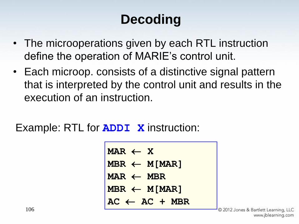
• The microoperations given by each RTL instruction
define the operation of MARIE’s control unit.
• Each microop. consists of a distinctive signal pattern
that is interpreted by the control unit and results in the
execution of an instruction.
Decoding
Example: RTL for ADDI X instruction:
MAR X
MBR M[MAR]
MAR MBR
MBR M[MAR]
AC AC + MBR
107
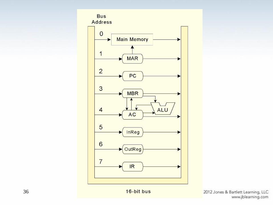
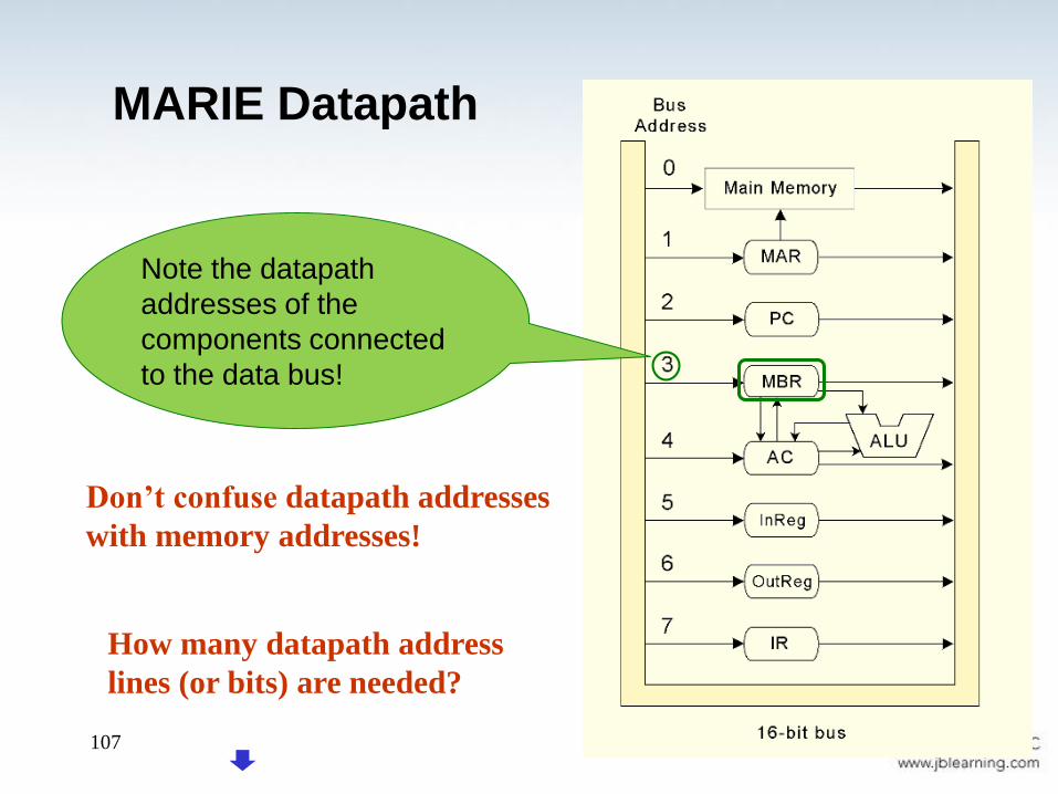
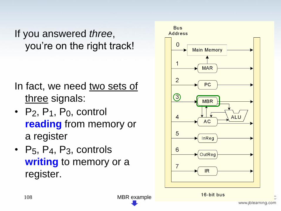
MARIE Datapath
Note the datapath
addresses of the
components connected
to the data bus!
How many datapath address
lines (or bits) are needed?
Don’t confuse datapath addresses
with memory addresses!
108
If you answered three,
you’re on the right track!
In fact, we need two sets of
three signals:
• P2, P1, P0, control
reading from memory or
a register
• P5, P4, P3, controls
writing to memory or a
register.
MBR example
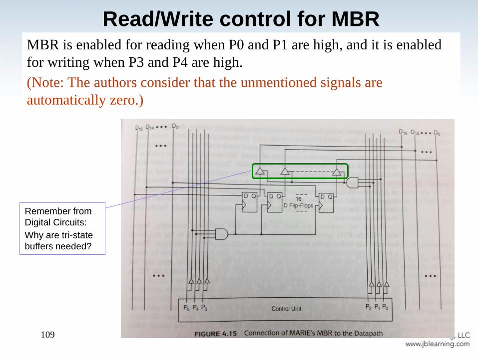
109
Read/Write control for MBRMBR is enabled for reading when P0 and P1 are high, and it is enabled
for writing when P3 and P4 are high.
(Note: The authors consider that the unmentioned signals are
automatically zero.)
Remember from
Digital Circuits:
Why are tri-state
buffers needed?
110
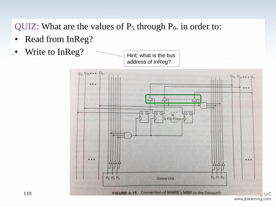
QUIZ: What are the values of P5 through P0. in order to:
• Read from InReg?
• Write to InReg? Hint: what is the bus
address of InReg?
111
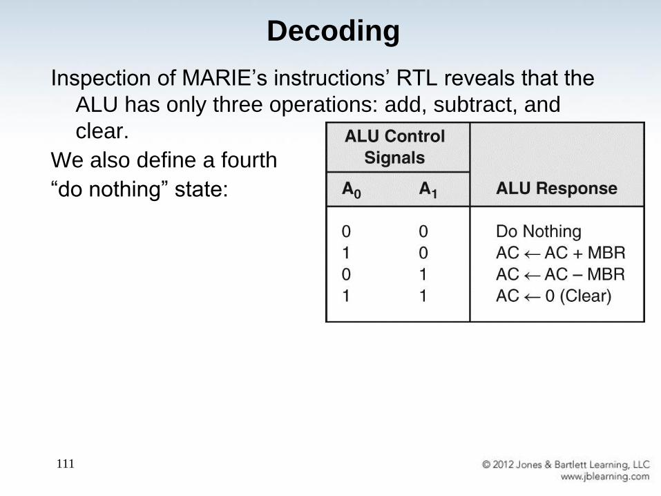
Inspection of MARIE’s instructions’ RTL reveals that the
ALU has only three operations: add, subtract, and
clear.
We also define a fourth
“do nothing” state:
Decoding
112
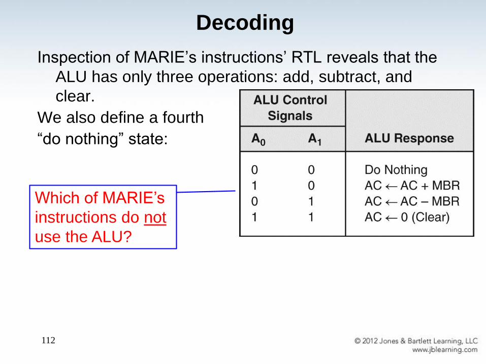
Inspection of MARIE’s instructions’ RTL reveals that the
ALU has only three operations: add, subtract, and
clear.
We also define a fourth
“do nothing” state:
Decoding
Which of MARIE’s
instructions do not
use the ALU?
113
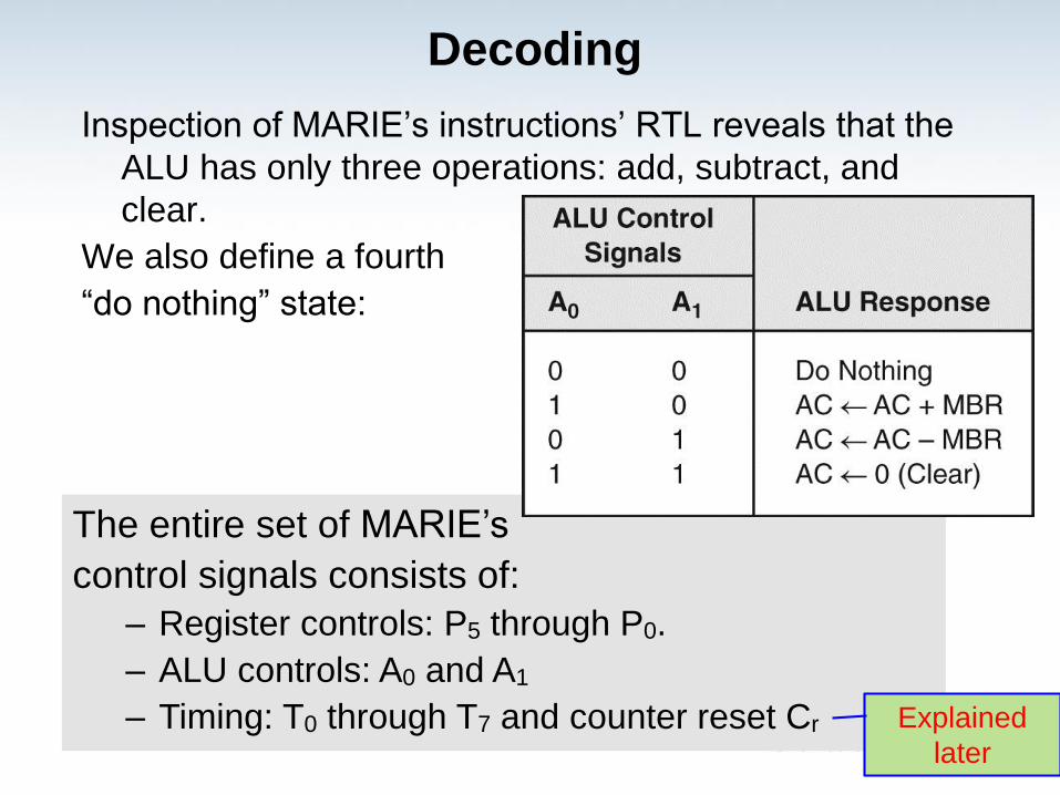
Inspection of MARIE’s instructions’ RTL reveals that the
ALU has only three operations: add, subtract, and
clear.
We also define a fourth
“do nothing” state:
Decoding
The entire set of MARIE’s
control signals consists of:
– Register controls: P5 through P0.
– ALU controls: A0 and A1
– Timing: T0 through T7 and counter reset Cr Explained
later
114
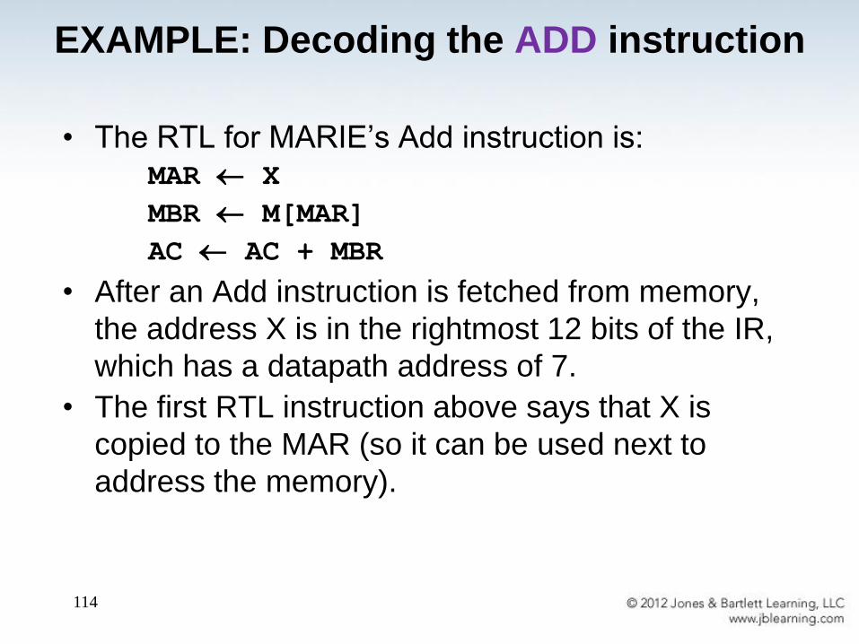
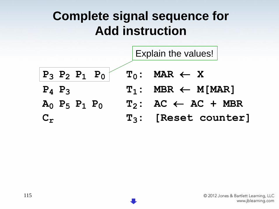
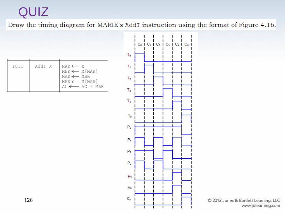
• The RTL for MARIE’s Add instruction is:MAR X
MBR M[MAR]
AC AC + MBR
• After an Add instruction is fetched from memory,
the address X is in the rightmost 12 bits of the IR,
which has a datapath address of 7.
• The first RTL instruction above says that X is
copied to the MAR (so it can be used next to
address the memory).
EXAMPLE: Decoding the ADD instruction
115
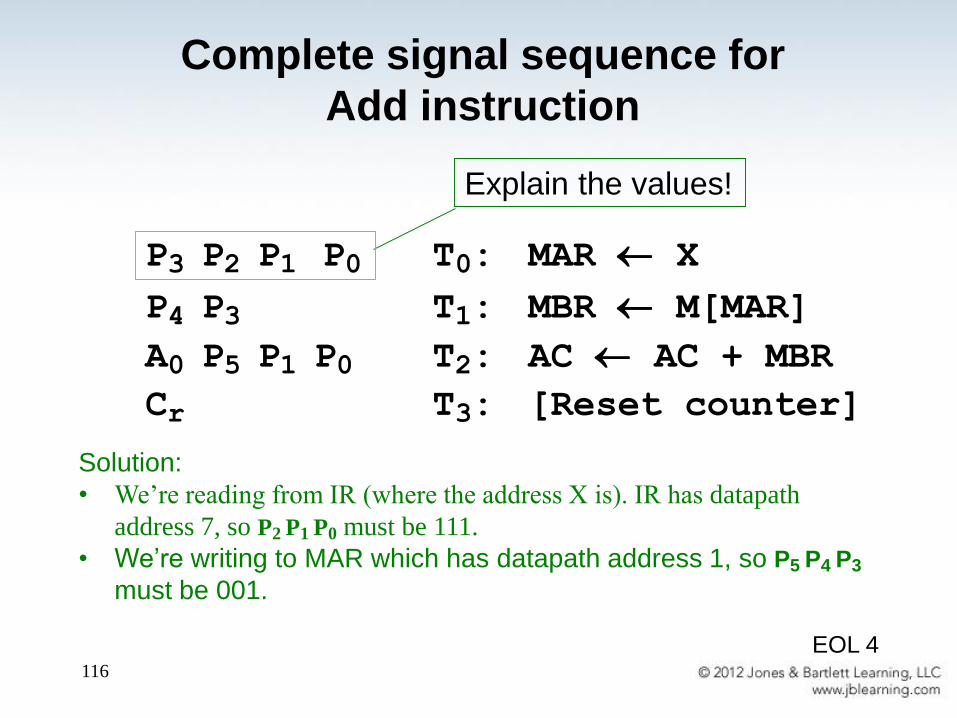
P3 P2 P1 P0 T0: MAR X
P4 P3 T1: MBR M[MAR]
A0 P5 P1 P0 T2: AC AC + MBR
Cr T3: [Reset counter]
Complete signal sequence for
Add instruction
Explain the values!
116
P3 P2 P1 P0 T0: MAR X
P4 P3 T1: MBR M[MAR]
A0 P5 P1 P0 T2: AC AC + MBR
Cr T3: [Reset counter]
Complete signal sequence for
Add instruction
Explain the values!
Solution:
• We’re reading from IR (where the address X is). IR has datapath
address 7, so P2 P1 P0 must be 111.
• We’re writing to MAR which has datapath address 1, so P5 P4 P3
must be 001.
EOL 4

117
P3 P2 P1 P0 T0: MAR X
P4 P3 T1: MBR M[MAR]
A0 P5 P1 P0 T2: AC AC + MBR
Cr T3: [Reset counter]
Complete signal sequence for
Add instruction
Explain the values!

118
P3 P2 P1 P0 T0: MAR X
P4 P3 T1: MBR M[MAR]
A0 P5 P1 P0 T2: AC AC + MBR
Cr T3: [Reset counter]
Complete signal sequence for
Add instruction
Explain the values!
119
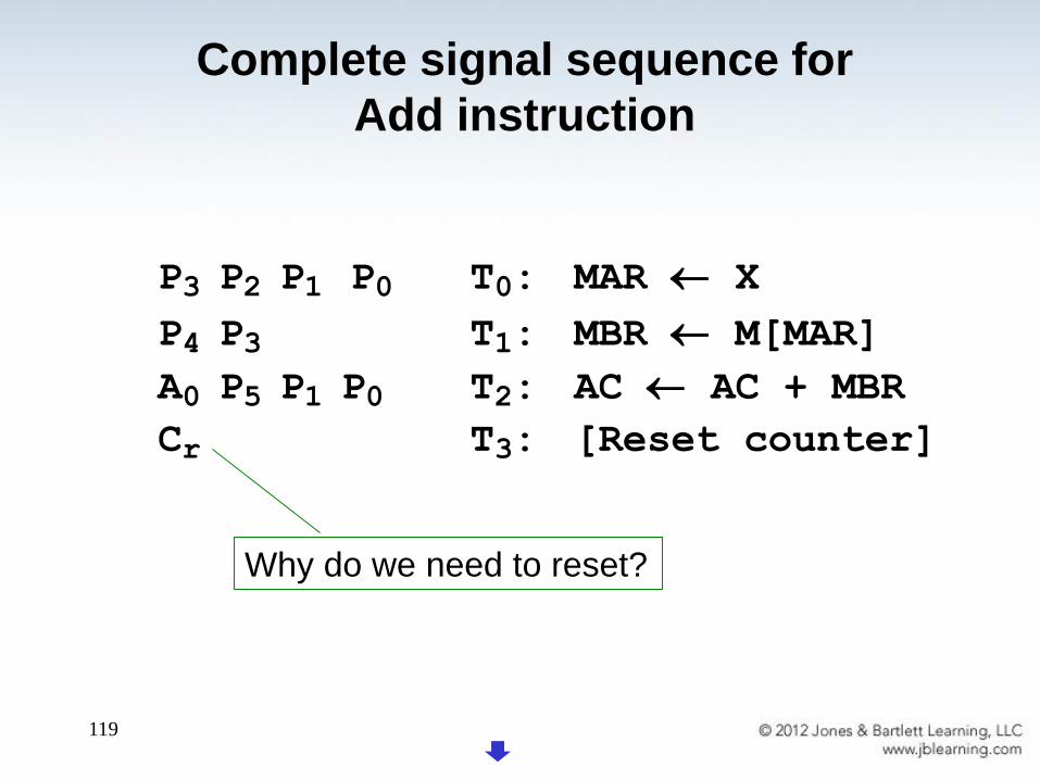
P3 P2 P1 P0 T0: MAR X
P4 P3 T1: MBR M[MAR]
A0 P5 P1 P0 T2: AC AC + MBR
Cr T3: [Reset counter]
Complete signal sequence for
Add instruction
Why do we need to reset?
120
What is the maximum nr. of
microops. needed for a MARIE
instruction?
Table 4.7 on p.252
121
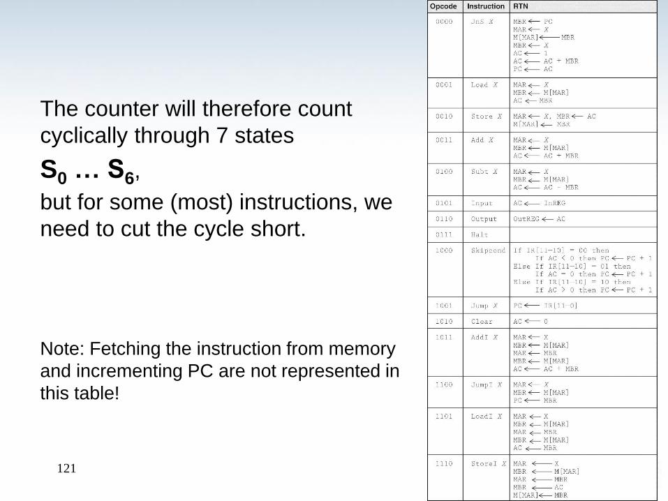
The counter will therefore count
cyclically through 7 states
S0 … S6,
but for some (most) instructions, we
need to cut the cycle short.
Note: Fetching the instruction from memory
and incrementing PC are not represented in
this table!
122
P3 P2 P1 P0 T0: MAR X
P4 P3 T1: MBR M[MAR]
A0 P5 P1 P0 T2: AC AC + MBR
Cr T3: [Reset counter]
Complete signal sequence for
Add instruction
How exactly are the timing signals used?
123
Timing diagram for
ADD
P3 P2 P1 P0 T0: MAR X
P4 P3 T1: MBR M[MAR]
A0 P5 P1 P0 T2: AC AC + MBR
Cr T3: [Reset counter]
The instruction bits in IR are constant
until the end of the current Fetch-
Execute cycle, but the Pi signals
need to change from one microop. to
the next!
QUIZ
124
Hint: How many clock cycles are needed?
Based on this, draw the timing signals Ti
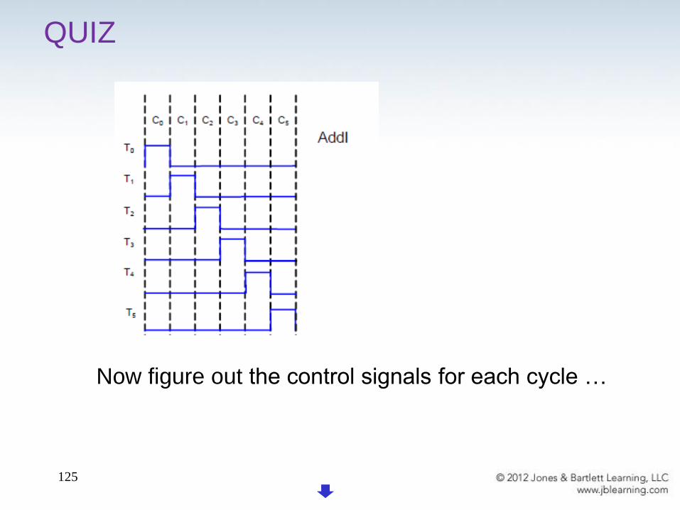
QUIZ
125
Now figure out the control signals for each cycle …
QUIZ
126
127
• The signal pattern described so far is the same
whether the CPU uses hardwired or
microprogrammed control.
• In hardwired control, the bit pattern of machine
instruction in the IR is decoded by combinational
logic.
• The decoder output works with the control signals
of the current system state to produce a new set
of control signals.
4.3.12 Decoding
128
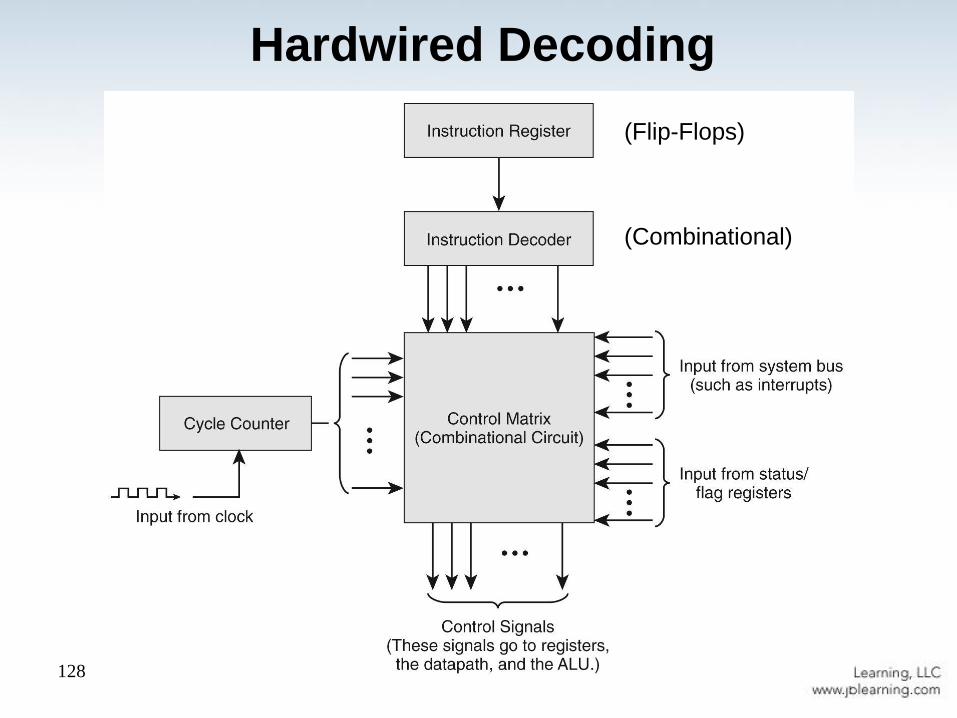
Hardwired Decoding
(Flip-Flops)
(Combinational)
129
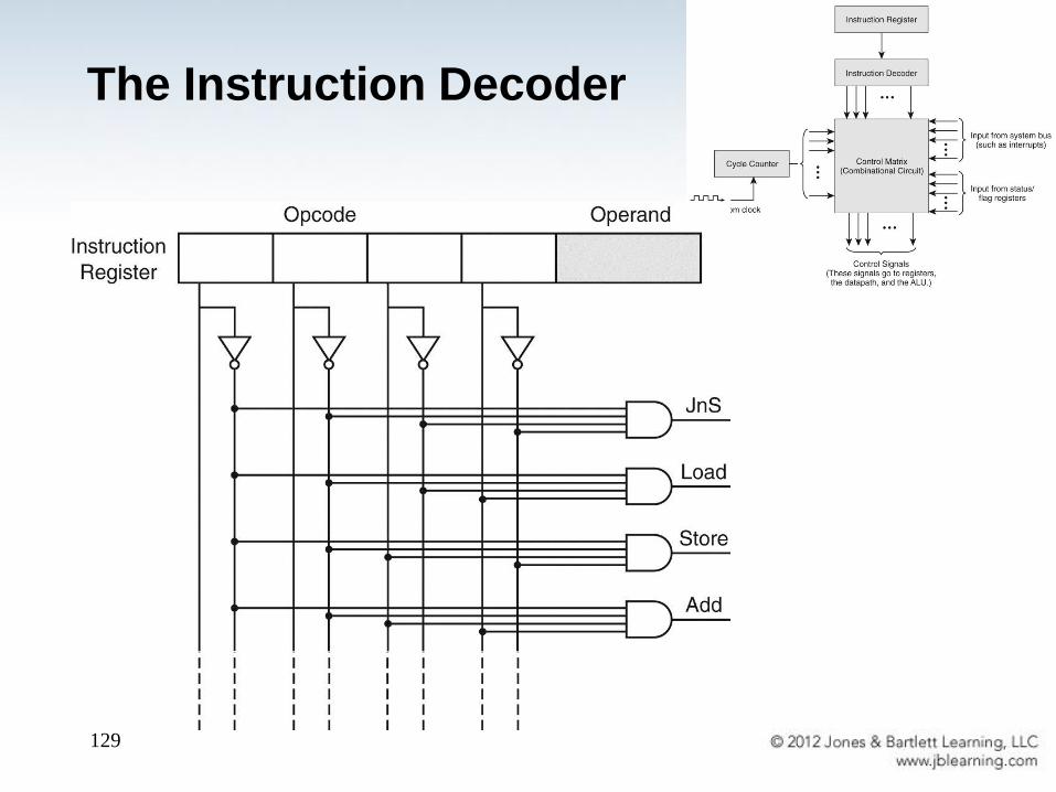
The Instruction Decoder
130
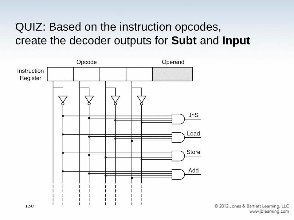
QUIZ: Based on the instruction opcodes,
create the decoder outputs for Subt and Input
131
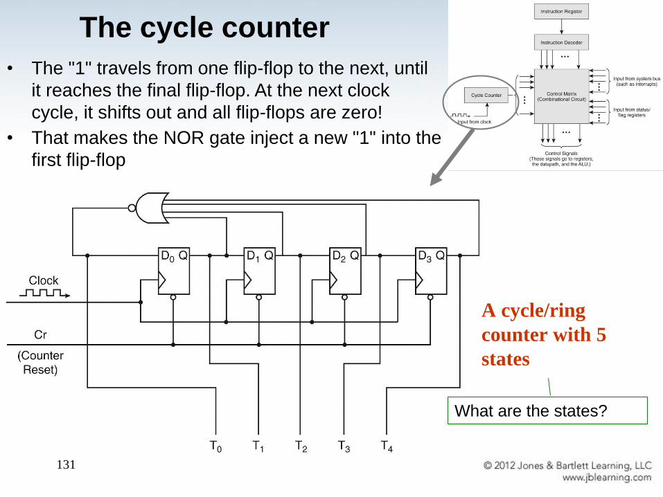
The cycle counter
A cycle/ring
counter with 5
states
What are the states?
• The "1" travels from one flip-flop to the next, until
it reaches the final flip-flop. At the next clock
cycle, it shifts out and all flip-flops are zero!
• That makes the NOR gate inject a new "1" into the
first flip-flop
132
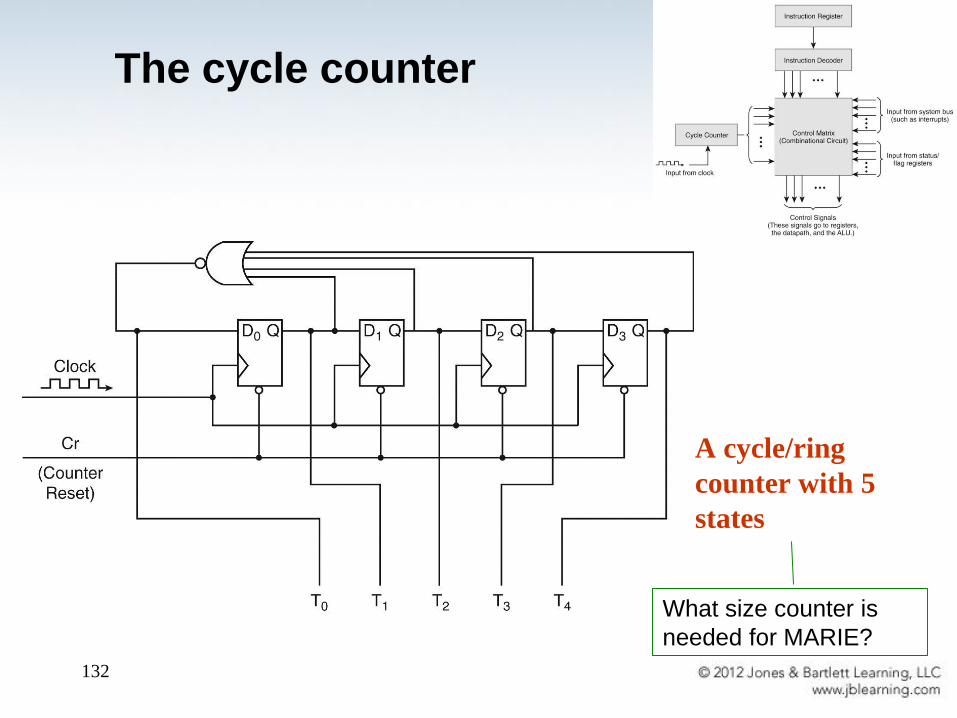
The cycle counter
A cycle/ring
counter with 5
states
What size counter is
needed for MARIE?

133
Hardwired control matrix for
Add (0011) instruction
Add

To do for next time:
Read and take notes: pp.255-62
Solve Exercise 55.
134
EOL 5

135
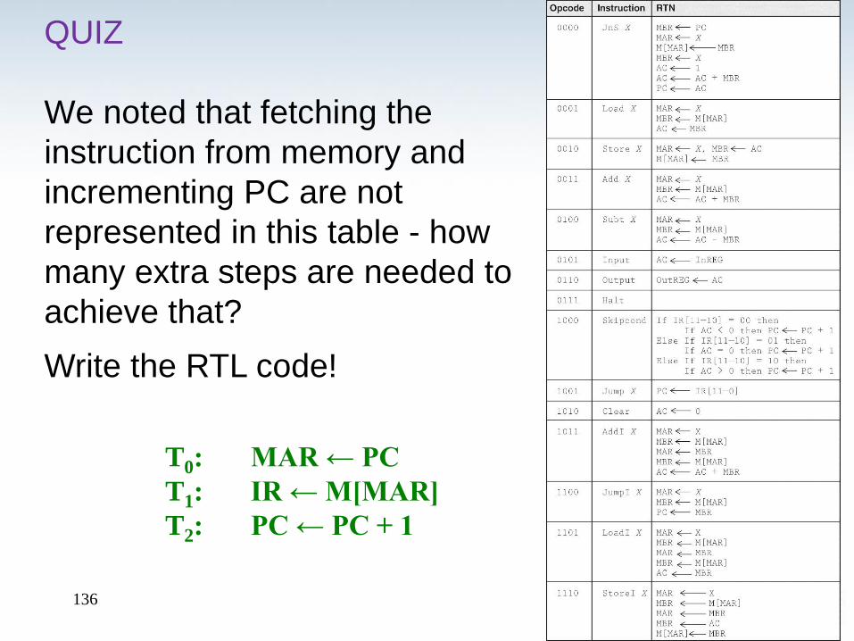
QUIZ
We noted that fetching the
instruction from memory and
incrementing PC are not
represented in this table - how
many extra steps are needed to
achieve that?
Write the RTL code!
136
QUIZ
We noted that fetching the
instruction from memory and
incrementing PC are not
represented in this table - how
many extra steps are needed to
achieve that?
Write the RTL code!
T0: MAR ← PC
T1: IR ← M[MAR]
T2: PC ← PC + 1

137
Extra-credit quiz

138
Second extra-credit quiz
139
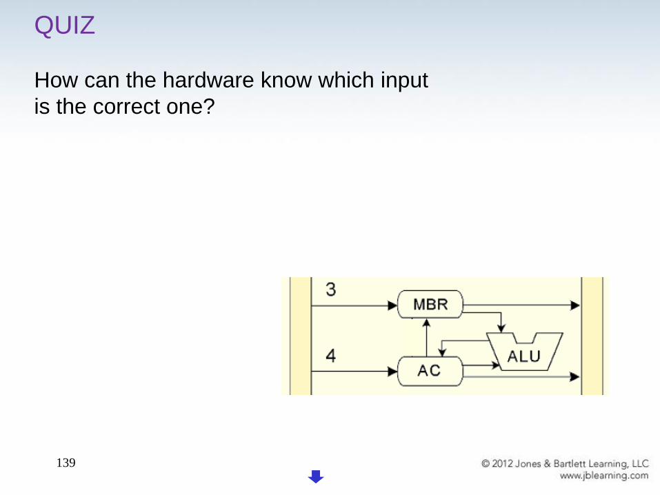
QUIZ
How can the hardware know which input
is the correct one?
140
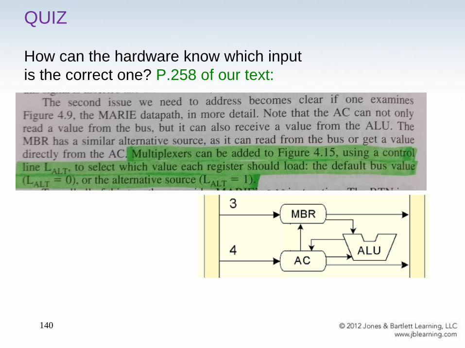
QUIZ
How can the hardware know which input
is the correct one? P.258 of our text:
141
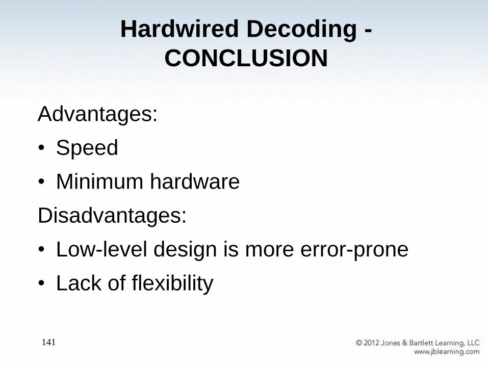
Advantages:
• Speed
• Minimum hardware
Disadvantages:
• Low-level design is more error-prone
• Lack of flexibility
Hardwired Decoding -
CONCLUSION
142
• The instruction microcode produces the changes
in the control signals.
• Machine instructions are the input for a
microprogram that converts the 1s and 0s of an
instruction into control signals.
• The microprogram is stored in firmware ROM,
a.k.a. the control store.
• A microcode instruction is retrieved during each
clock cycle.
4.13.2 Microprogrammed Decoding
143
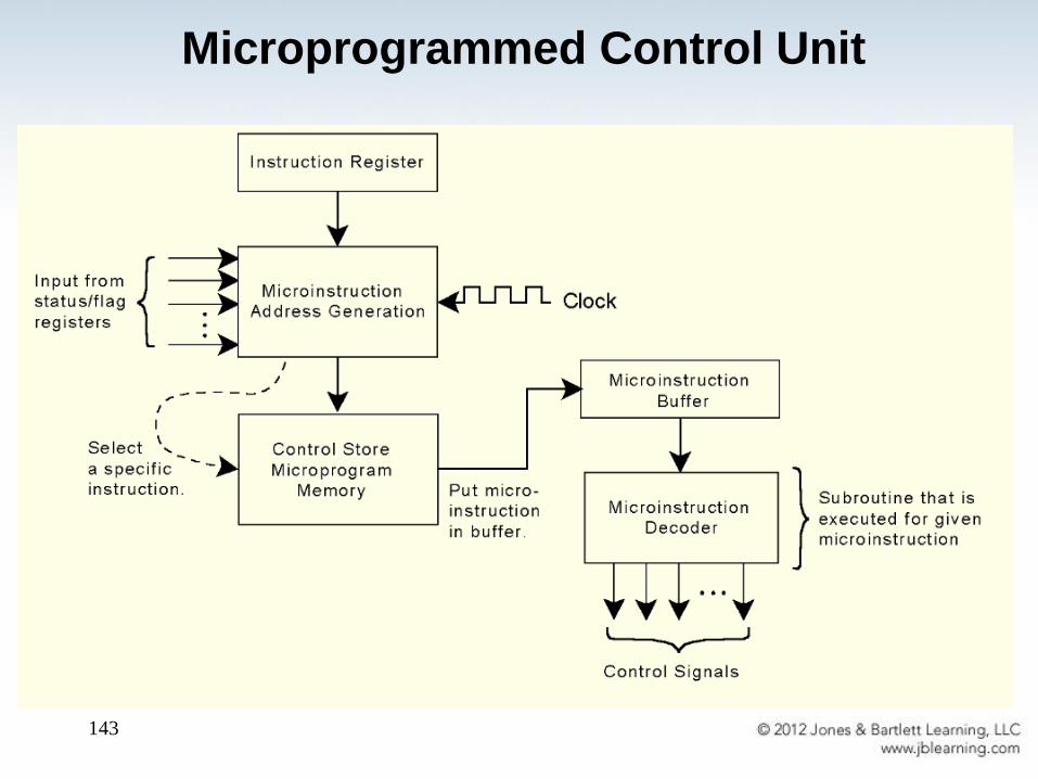
Microprogrammed Control Unit
144
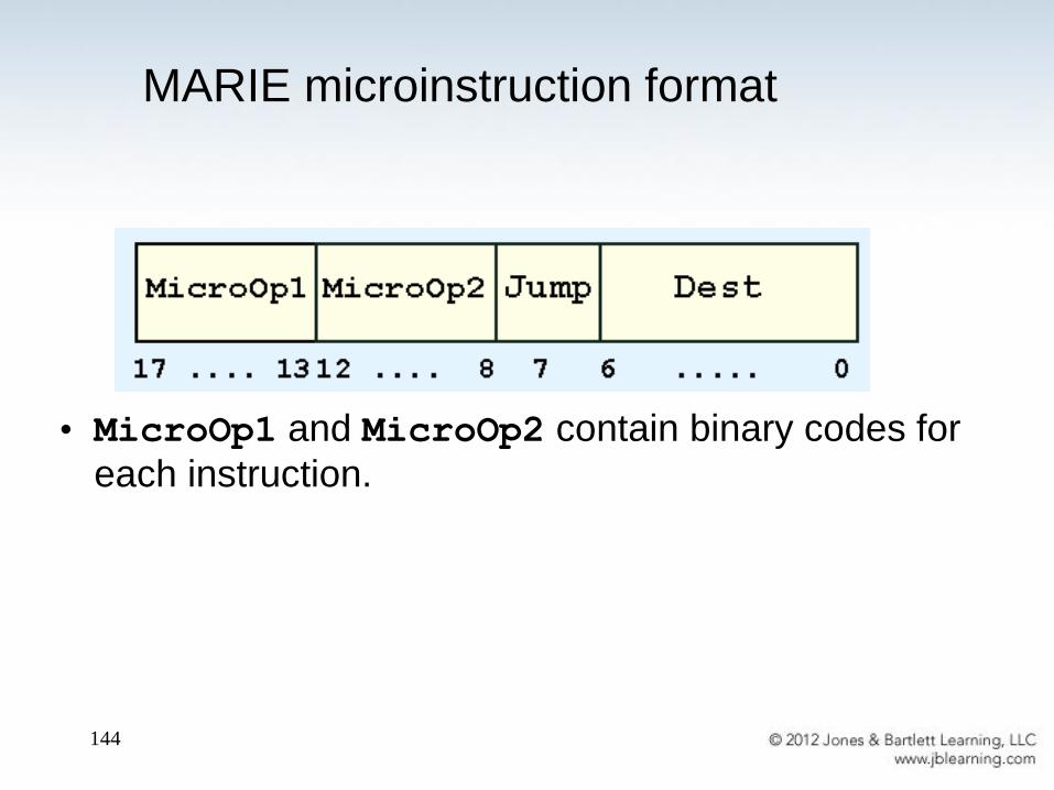
• MicroOp1 and MicroOp2 contain binary codes for
each instruction.
MARIE microinstruction format
145
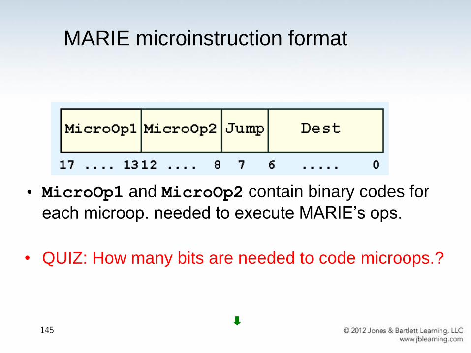
• MicroOp1 and MicroOp2 contain binary codes for
each microop. needed to execute MARIE’s ops.
• QUIZ: How many bits are needed to code microops.?
MARIE microinstruction format

146
Table 4.7 on p.252
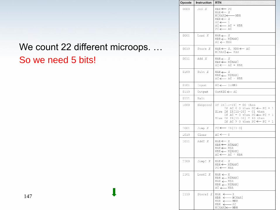
We count 22 different microops. …
147
We count 22 different microops. …
So we need 5 bits!

148
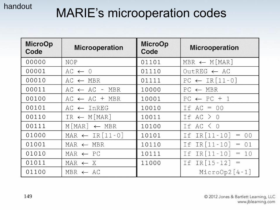
MARIE’s microoperation codes
Actually, for microprogramming purposes, we need 2 more microops.
149
MARIE’s microoperation codeshandout
150
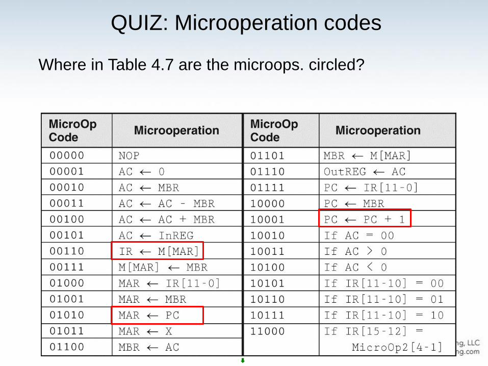
QUIZ: Microoperation codes
Where in Table 4.7 are the microops. circled?
151
QUIZ: Microoperation codes
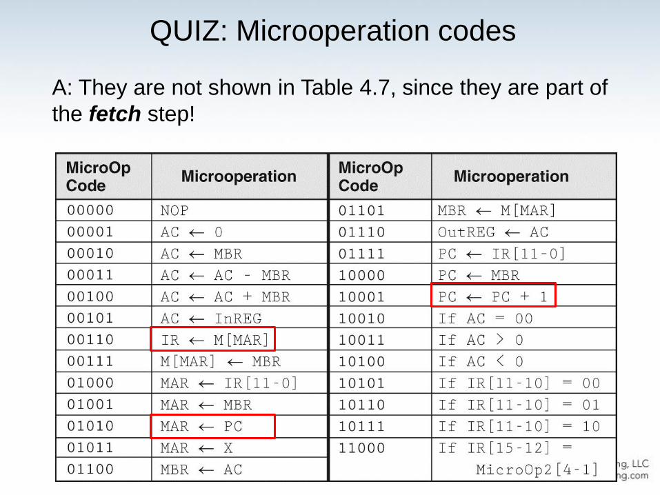
A: They are not shown in Table 4.7, since they are part of
the fetch step!
152
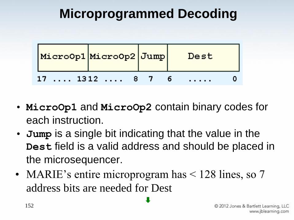
• MicroOp1 and MicroOp2 contain binary codes for
each instruction.
• Jump is a single bit indicating that the value in the
Dest field is a valid address and should be placed in
the microsequencer.
• MARIE’s entire microprogram has < 128 lines, so 7
address bits are needed for Dest
Microprogrammed Decoding
153
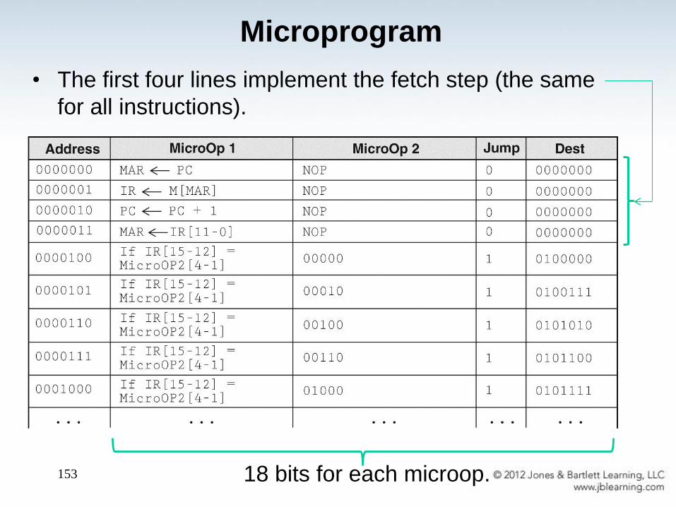
Microprogram
• The first four lines implement the fetch step (the same
for all instructions).
18 bits for each microop.
154
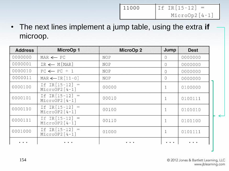
• The next lines implement a jump table, using the extra if
microop.
155
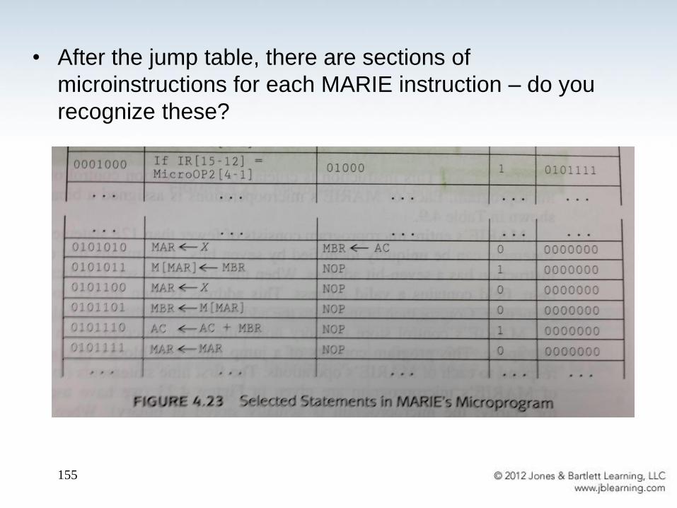
• After the jump table, there are sections of
microinstructions for each MARIE instruction – do you
recognize these?
156
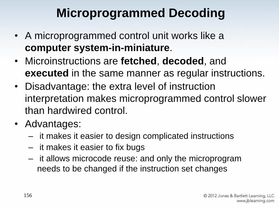
• A microprogrammed control unit works like a
computer system-in-miniature.
• Microinstructions are fetched, decoded, and
executed in the same manner as regular instructions.
• Disadvantage: the extra level of instruction
interpretation makes microprogrammed control slower
than hardwired control.
• Advantages:– it makes it easier to design complicated instructions
– it makes it easier to fix bugs
– it allows microcode reuse: and only the microprogram
needs to be changed if the instruction set changes
Microprogrammed Decoding
• Use the “Microprogramming” handout, so
we have easy access to all relevant figures
157
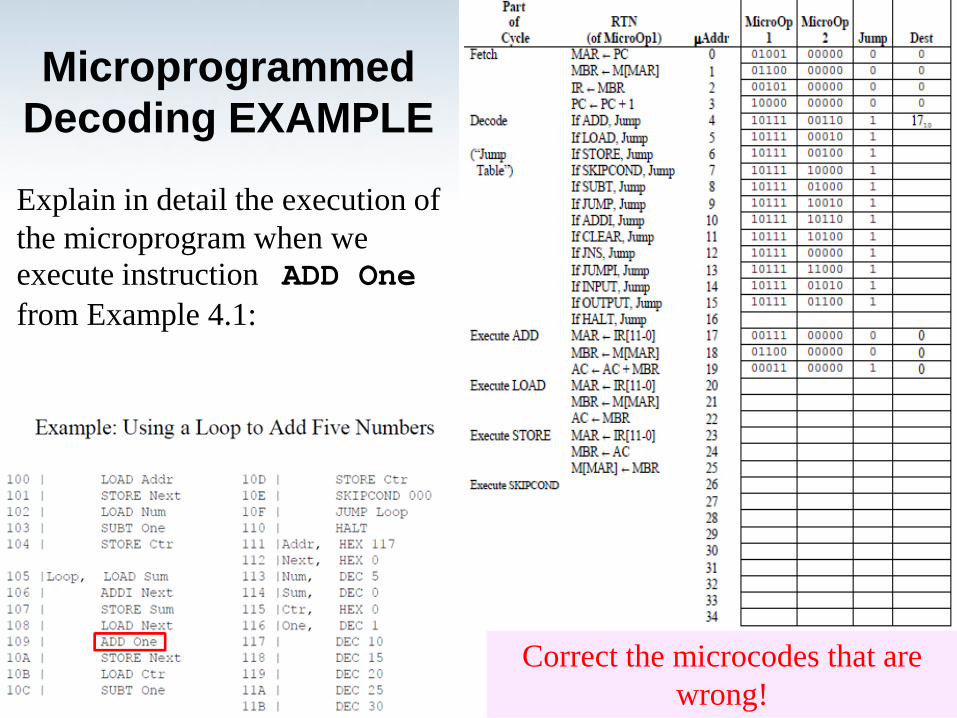
Explain in detail the execution of
the microprogram when we
execute instruction ADD One
from Example 4.1:
158
Microprogrammed
Decoding EXAMPLE
Correct the microcodes that are
wrong!
QUIZ
Explain in detail the execution
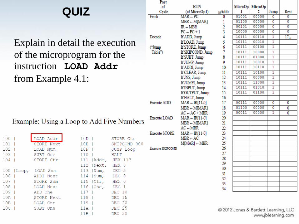
of the microprogram for the
instruction LOAD Addr
from Example 4.1:
159

4.14 Real World Architectures
• Read an take notes
• Check out the links on our webpage, under
Real-World ISAs
160

Homework for Ch.4:
9, 16, 21, 22, 45, 56, 57, 62
Due next Tuesday, Nov. 8
161