Chapter 3read.pudn.com/downloads114/ebook/480976/Fault-Tolerance Techniqu… · acceptable levels...
43
29 Chapter 3 SINGLE EVENT UPSET (SEU) MITIGATION TECHNIQUES State-of-the-Art The first SEU mitigation solution that has been used for many years in spacecraft was shielding, which reduces the particle flux to very low levels, but it does not completely eliminate it. This solution was sufficient to avoid errors caused by radiation effects for many years in the past. However, due to the continuous evolution of the fabrication technology process, as explained in last chapter, electronic circuits are becoming more and more sensitive to radiation particles, and the charged particles that once were negligible are now able to cause errors in the electronic design. Conse- quently, extra techniques must be applied to avoid radiation effects. Several SEU mitigation techniques have been proposed in the last few years in order to avoid faults in digital circuits, including those implemented in programmable logic. They can be classified as: - Fabrication process-based techniques, such as: • Epitaxial CMOS processes • Advanced process such as silicon-on-insulator (SOI). - Also there are Design-based techniques, such as: • Detection techniques: Hardware redundancy Time redundancy EDC (error detection coding) Self-checker techniques
Transcript of Chapter 3read.pudn.com/downloads114/ebook/480976/Fault-Tolerance Techniqu… · acceptable levels...

29
Chapter 3
SINGLE EVENT UPSET (SEU) MITIGATION TECHNIQUES State-of-the-Art
The first SEU mitigation solution that has been used for many years in spacecraft was shielding, which reduces the particle flux to very low levels, but it does not completely eliminate it. This solution was sufficient to avoid errors caused by radiation effects for many years in the past. However, due to the continuous evolution of the fabrication technology process, as explained in last chapter, electronic circuits are becoming more and more sensitive to radiation particles, and the charged particles that once were negligible are now able to cause errors in the electronic design. Conse-quently, extra techniques must be applied to avoid radiation effects.
Several SEU mitigation techniques have been proposed in the last few years in order to avoid faults in digital circuits, including those implemented in programmable logic. They can be classified as:
- Fabrication process-based techniques, such as:
• Epitaxial CMOS processes
• Advanced process such as silicon-on-insulator (SOI).
- Also there are Design-based techniques, such as:
• Detection techniques:
Hardware redundancy
Time redundancy
EDC (error detection coding)
Self-checker techniques

30 Chapter 3
• Mitigation techniques:
Triple Modular Redundancy (TMR)
Multiple redundancy with voting
EDAC (Error detection and correction coding)
Hardened memory cell level
- And Recovery Techniques (applied to programmable logic only), such as:
• Reconfiguration
• Partial configuration
• Rerouting design
The fabrication process-based techniques, also called technological
techniques, such as epitaxial CMOS process and silicon-on-insulator (IBM, 2000; Colinge, 2001; Musseau and Ferlet-Cavrois, 2001), can reduce to acceptable levels some of the radiation effects, such as Total Ionization Dose (TID) effects and single event latch-up (SEL), however, they do not completely eliminate upset effects, such as single event upsets (SEUs) and single transient effect (SET). The fabrication process-based solution is expensive and consequently very few designs have adopted this technique, especially for low volume production. In (Irom et al., 2002), SEU effects from heavy ions and protons are measured for Motorola and IBM silicon-on-insulator microprocessors, and compared with results from similar devices with bulk substrates. Results show that the threshold LET values of the SOI processors are nearly the same as those of bulk/epi processors from the same manufactures, indicating that little improvement in SEU sensitivity has resulted from the move to SOI technology. Although the threshold LET did not change, the cross section of the SOI processors were about an order of magnitude lower than the bulk/epi counterparts, leading to a lower upset rate in the space environment. These results show that only modest improve-ments in SEU sensitivity can be expected as mainstream integrated circuits move to SOI technology, and consequently design-based techniques must be applied to mitigate SEU.
The design-based techniques, also called architectural techniques, are highly accepted because they can be applied to many different levels of the design without any changes in the fabrication process technology. They can be planned to just detect the presence of an upset in the system or they can be more complex in order to detect and correct the system error in the presence of an upset. All design-based techniques are composed of some

SINGLE EVENT UPSET (SEU) MITIGATION TECHNIQUES 31
kind of redundancy, which can be provided by extra components (hardware redundancy) or by an extra execution time or by different instants of data sampling (time redundancy). Very often, techniques implement a combi-nation of both.
Hardware redundancy is basically based on logic redundancy, which is characterized as extra components or extra paths that allow the design to continue operation even when some parts fail. Error detection and correction codes (EDAC) can also been seen as a hardware redundancy because it generates redundant bits to be able to detect and correct upsets. EDAC codes can be also used in time redundancy techniques, as it is going to be discussed in next sections. By concerning only the SEU problem in storage devices, hardened memory cells is another example of hardware redundancy that can be applied to avoid error in memories.
Recently, new techniques based on recovery have been proposed particularly for programmable logic components, such as SRAM-based FPGAs. The idea is to recover the original programmed information after an upset. Examples of this technique are reconfiguration (scrubbing), partial reconfiguration and rerouting design. They are able to clean out an upset in the programmable matrix in a very short period of time. This type of technique is usually used to avoid the accumulation of upsets.
Finding the most appropriate SEU mitigation solution has become a challenge in order to combine fast turnaround time, low cost, high per-formance and high reliability. An efficient set of SEU mitigation techniques should cope with transient faults (SET) occurring in the combinational logic and SEUs in the storage cells. In this way, transient faults in the combinational logic will never be stored in the storage cells, and bit flips in the storage cells will never occur or will be immediately corrected. Each technique has some advantages and drawbacks, and there is always a compromise between area, performance, power dissipation and fault tolerance efficiency.
This chapter presents an overview of the design-based techniques on digital circuits, and subsequently it shows the state o the art of SEU mitigation techniques for ASICs and FPGAs, including solutions using the recovery method.
3.1 DESIGN-BASED TECHNIQUES
Time and hardware redundancy techniques are largely used in ASICs (Nicolaidis, 1999; Dupont et al., 2002; Benz et al., 2002). The techniques range from simple upset detection to upset voting and correction. There is a wide choice of techniques according to the user’s application requirements.

32 Chapter 3
Sometimes it is just necessary to warn the presence of an upset with an interruption in the system functionality, while sometimes it is required to completely avoid interruptions, assuring full reliability. There is a set of techniques that can present reliability in between these two extremes, each one producing more or less overhead according to its robustness in the presence of a fault.
3.1.1 Detection Techniques
Techniques based on time redundancy are usually used to detect a transient effect (SET) in the combinational logic, while hardware redundancy can help to identify an SEU in the sequential logic. Examples of the use of time and hardware redundancy for SET detection have been presented in the (Nicolaidis, 1999; Anghel et al., 2000; Dupont et al., 2002). In the case of time redundancy, the goal is to take advantage of the characteristics of the transient pulse generated by the particle strike to compare the output signals at two different moments. The output of the combinational logic is latched at two different times, where the clock edge of the second latch is shifted by time d. A comparator indicates a transient pulse occurrence (error detection). The scheme is illustrated in figure 3-1.
clk
clk+d
Combinational logic
D Q
D Q
A0B0C0
error
Figure 3-1. Time redundancy duplication scheme to detect SET in combinational logic
In the case of hardware redundancy, the duplication with comparison (DWC) scheme can be used for both combinational and sequential logic to SET and SEU detection, respectively. Figures 3-2 and 3-3 show the schemes for transient effect detection. Note that for both techniques, time and hardware redundancy, it is important to take into account the duration of the SET.
Another example of upset detection for sequential logic is error-detecting codes such as parity bits. In this case, the parity bit of a group of analyzed bits is calculated and it is continuously compared to a new parity bit calculation. If a SEU has occurred, it is possible to detect it. This solution is largely used nowadays in memories. However, for high-reliability applications, sometimes it is not enough only to detect the presence of a

SINGLE EVENT UPSET (SEU) MITIGATION TECHNIQUES 33
fault, rather one has to ensure the correct operation of the system in the presence of that fault. For this reason, it is very important to investigate in detail the SEU mitigation solutions.
Combinational logic
Combinational logic
A0B0C0
A1B1C1
error
Figure 3-2. Hardware redundancy duplication scheme to detect SET in combinational logic
clk
clk
D Q
D Q
in0
in1
error
Figure 3-3. Hardware redundancy duplication scheme to detect SEU in sequential logic
3.1.2 Mitigation Techniques
3.1.2.1 Full Time and Hardware Redundancy
The use of full time redundancy in the combinational logic permits voting the correct output value in the presence of a SET. The name full redundancy comes from the complete n-modular redundancy, where n is equal to three: triple modular redundancy. In this case, the output of the combinational logic is latched at three different moments, where the clock edge of the second latch is shifted by the time delay d and the clock of the third latch is shifted by the time delay 2.d. A voter chooses the correct value. The full time redundancy scheme is illustrated in figure 3-4 and the majority voter scheme is presented in figure 3-5. The area overhead comes from the extra sample latches and the performance penalty is given by clk+2.d+tp, where d depends on the duration of the transient current pulse and tp is the delay from the majority voter. The total delay is measured by the error pulse width multiplied by 2, which is approximately equal to 2 x (QCOL / ID).

34 Chapter 3
clk
clk+d
Combinational logic
clk+2d
MAJ
A0B0C0
out
D Q
D Q
D Q
Figure 3-4. Full time redundancy scheme to correct SET in combinational logic
A
B
C
V
A B C V
01010101
00110011
00001111
00010111
Figure 3-5. Majority Voter Schematic and the Truth Table
In the case of the full hardware redundancy, the well-known Triple
Modular Redundancy (TMR) approach, the logic is triplicated and voters are placed at the output to identify the correct value. The first possibility that was largely used in space applications is the triplication of the entire device, figure 3-6. This approach uses a voter as a fourth component in the board. It needs extra connections and it presents area overhead. If an error occurs in one of the three devices, the voter will choose the correct value. It protects both combinational and sequential logic against upsets. However, if an upset occurs in the voter, the TMR scheme is ineffective and a wrong value will be present in the output. Another problem of this approach is the accumulation of upsets, hence an extra mechanism is necessary to correct the upset in each device before the next SEU happens.

SINGLE EVENT UPSET (SEU) MITIGATION TECHNIQUES 35
Device0
Device1
Device2
voter
in0
in1
in2
out
Figure 3-6. TMR implemented in the entire device
A more efficient implementation of the TMR is applied focused in the sensitive logic, for example the memory cells to protect against SEU, see figure 3-7.
MAJ
clk
Sequential logic
Combinational logic
A0B0C0
D Q
D Q
D Q
out
Figure 3-7. TMR Memory Cell with Single Voter
However, this solution does not avoid the accumulation of upsets in the sequential logic and the voter is vulnerable to upsets. In order to restore the corrected value, a solution using three voters with a feedback was proposed (Carmichael, 2001; Katz et al., 2001), figure 3-8. The upsets in the latches are corrected by extra logic in order to avoid accumulation. The load frequency (refreshing) can be set by the multiplexor control signal.

36 Chapter 3
Sequential logic
clkMAJ
MAJ
MAJclk
clk
in0
in1
in2
D Q
D Q
D Q
Q0Q1Q2
Q0Q1Q2
Q0Q1Q2
trv0
trv1
trv20
1
0
1
0
1
e2
e1
e0
Q0
Q1
Q2
Figure 3-8. TMR memory cell with three voters and refreshing (version I)
The combinational logic must also be protected to avoid SET. There are many possibilities. One is to use time redundancy in the logic as shown in figure 3-9. Another possibility is to triplicate the combinational logic as well, as represented in figure 3-10.
Although the last proposed implementation of the TMR (figure 3-10) presents a larger area overhead compared to time redundancy, since it triplicates all the combinational and sequential logic, it protects the logic against SET and SEU, and avoids accumulation of upsets. In addition, it does not have major performance penalties, just the voter propagation time, and it does not need different clock phases.
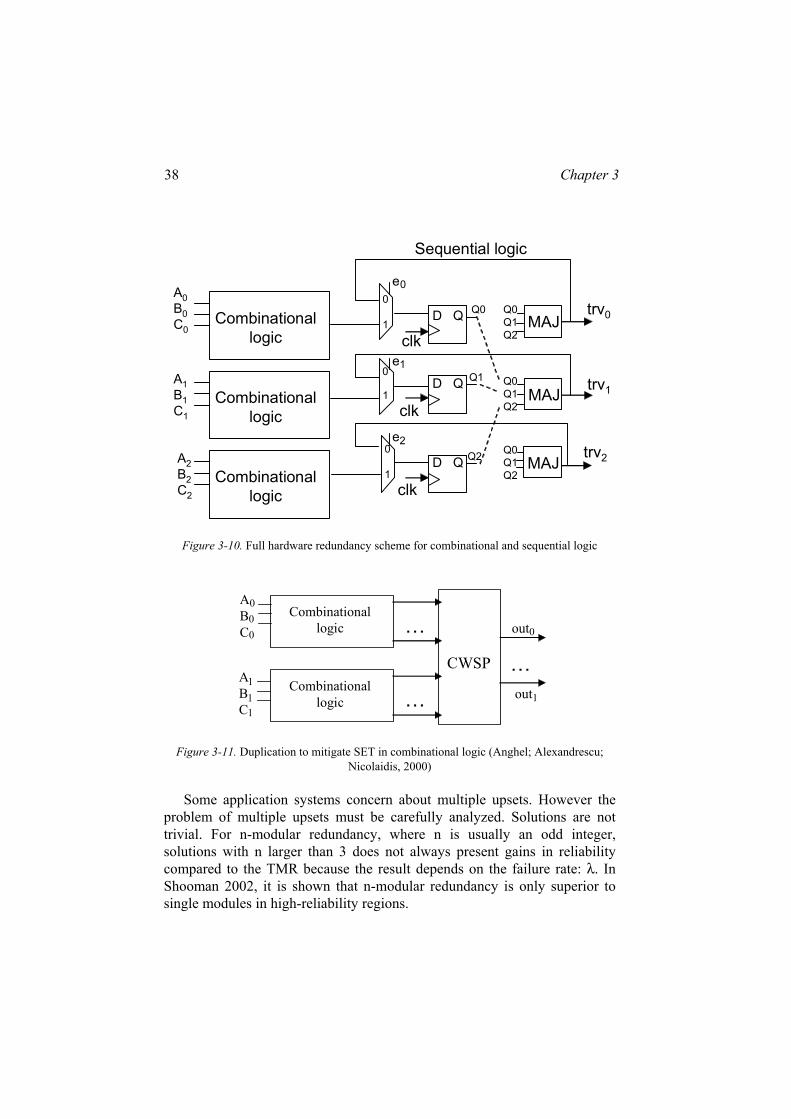
Another method to mitigate SET in combinational logic is based on duplication and a code word state preserving (CWSP) (Anghel et al., 2000), as illustrated in figure 3-11. This method does not need voters or comparators. The duplication can be replaced by time redundancy as well, which reduces the area overhead significantly, figure 3-12. The main contribution of this method is the CWSP stage, which replaces the last gates of the circuit by a particular gate topology, which is able to pass the correct value in the combinational logic in the presence of a SET, figure 3-13. Additional techniques to cope with SET are presented in (Alexandrescu et al., 2002).

SINGLE EVENT UPSET (SEU) MITIGATION TECHNIQUES 37
Seq
uent
ial l
ogic
clk
MA
J
MA
J
MA
Jcl
k
clk
D
Q
D
Q
D
Q
Q0
Q1
Q2
Q0
Q1
Q2
Q0
Q1
Q2
trv trv trv0 10 10 1
ee 1e 0
clk
clk+
d
Com
bina
tiona
l lo
gic
clk+
2d
MA
J
MA
J
A0
B0
C0
MA
JD
Q
D
Q
D
Q
Seq
uent
ial l
ogic
clk
MA
J
MA
J
MA
Jcl
k
clk
D
Q
D
Q
D
Q
Q0
Q1
Q2
Q0
Q1
Q2
Q0
Q1
Q2
trv0
trv1
trv2
0 10 10 1
e 2ee
clk
clk+
d
Com
bina
tiona
l lo
gic
clk+
2d
MA
J
MA
J
A0
B0
C0
MA
JD
Q
D
Q
D
Q
Figure 3-9. Full time redundancy scheme for combinational logic combined to full hardware redundancy in the sequential logic
38 Chapter 3
Combinational logic
Combinational logic
Combinational logic
Sequential logic
clkMAJ
MAJ
MAJclk
clk
D Q
D Q
D Q
Q0Q1Q2
Q0Q1Q2
Q0Q1Q2
trv0
trv1
trv20
1
0
1
0
1
e2
e1
e0
Q0
Q1
Q2
A0B0C0
A1B1C1
A2B2C2
Figure 3-10. Full hardware redundancy scheme for combinational and sequential logic
Combinational logic
Combinational logic
CWSP
…
…
…
A0B0C0
A1B1C1
out0
out1
Figure 3-11. Duplication to mitigate SET in combinational logic (Anghel; Alexandrescu; Nicolaidis, 2000)
Some application systems concern about multiple upsets. However the problem of multiple upsets must be carefully analyzed. Solutions are not trivial. For n-modular redundancy, where n is usually an odd integer, solutions with n larger than 3 does not always present gains in reliability compared to the TMR because the result depends on the failure rate: λ. In Shooman 2002, it is shown that n-modular redundancy is only superior to single modules in high-reliability regions.

SINGLE EVENT UPSET (SEU) MITIGATION TECHNIQUES 39
Combinational logic
CWSP
…
…d
A0B0C0
out0
out1
Figure 3-12. Time redundancy to mitigate SET in combinational logic (Anghel; Alexandrescu; Nicolaidis, 2000)
in
in*
out
Figure 3-13. Example of INVERTER logic with the code word state preserving (CWSP) in the duplication and time redundancy to mitigate SET in combinational logic
3.1.2.2 Error Correction and Detection Codes
Error detection and correction coding (EDAC) technique (Peterson, 1980) is also used to mitigate SEU in integrated circuits. It is usually used in memory. There are many codes to be used to protect the systems against single and multiple SEUs. An example of EDAC is the hamming code (Houghton, 1997) in its simplest version. It is an error-detecting and error-correcting binary code that can detect all single- and double-bit errors and correct all single-bit errors (SEC-DED). This coding method is recom-mended for systems with low probabilities of multiple errors in a single data structure (e.g., only a single bit error in a byte of data). The code satisfies the relation 2k ≥ m+k+1, where m+k is the total number of bits in the coded word, m is the number of information bits in the original word, and k is the number of check bits in the coded word. Following this equation the

40 Chapter 3
hamming code can correct all single-bit errors on n-bit words and detect double-bit errors when an overall parity check bit is used.
The hamming code implementation is composed of a combinational block responsible for encoding the data (encoder block), inclusion of extra bits in the word that indicate the parity (extra latches or flip-flops) and another combinational block responsible for decoding the data (decoder block). The encoder block calculates the parity bit and it can be implemented by a set of 2-input XOR gates. The decoder block is more complex than the encoder block, because it needs not only to detect the fault, but it must also correct it. It is basically composed of the same logic used to compose the parity bits plus a decoder that will indicate the bit address that contains the upset. The decoder block can also be composed of a set of 2-input XOR gates and some AND and INVERTER gates.
The encoder block calculates the check bits that are placed in the coded word at positions 1, 2, 4, …, 2(k-1). For example, for 8-bit data, 4 check bits (p1, p2, p3, p4) are necessary, so that the hamming code is able to detect and correct a single-bit error (SEC-SED). Figure 3-14 demonstrates a 12-bit coded word (m = 8 and k = 4) with the check bits p1, p2, p3 and p4 located at positions 1, 2, 4 and 8 respectively. The check bits are able to inform the position of the error. The encoder block can be implemented by a set of 2-input XOR gates. For an 8-bit data, 14 2-input XOR gates are necessary in order to generate the 4 parity bits. The check bit p1 creates even parity for the bit group {1, 3, 5, 7, 9, 11}. The check bit p2 creates even parity for the bit group {2, 3, 6, 7, 10, 11}. Similarly, p3 creates an even parity for the bit group {4, 5, 6, 7, 12}. Finally, the check bit p4 creates even parity for the bit group {8, 9, 10, 11, 12}.
coded wordp1 p2 p4 p8
p1
p2
p4
p8
word
Figure 3-14. Hamming code check bits generation for a 8-bit word, 12-bit coded word

SINGLE EVENT UPSET (SEU) MITIGATION TECHNIQUES 41
Hamming code can protect structures such as registers, register files and memories. Each protected register must have its input connected to the encoder block, and its output connected to the decoder block. Note that only one register may be used at a clock cycle. The main advantage of the set of registers structure is that only one encoder block and one decoder block are multiplexed for a set of registers.
Hamming code increases area by requiring additional storage cells (check bits), plus the encoder and the decoder blocks. For an n bit word, there are approximately log2n more storage cells. However, the encoder and decoder blocks may add a more significant area increase, thanks for the extra XOR gates. Regarding performance, the delay of the encoder and decoder block is added in the critical path. The delay gets more critical when the number of bits in the coded word increases. The number of XOR gates in serial is directly proportional to the number of bits in the coded word.
Table 3.1 shows a comparison between hamming code and the full hardware redundancy (TMR) to mitigate SEU in sequential circuits. Results published in (Hentschke et al., 2002) show that TMR is more efficient in terms of area and performance to protect registers and small memory structures, while hamming code is more appropriate to protect large register files and memories.
Table 3-1. Hamming Code and TMR Comparison Summary Hamming Code (SEC-
DED) TMR
Area It depends on the number of bits to be protected. It has a small overhead of storage cells (parity cells) It needs additional combinational logic to implement the encoder and the decoder blocks in the case of short coded words.
It needs 3 times more storage cells. It needs small extra logic for the voters. The number of voters is proportional to the number of storage cells.
Performance The encoder and decoder blocks, which are located in the critical path, can affect the performance. The delay increases pro-portionally to the number of bits to be coded because of the number of XOR
The performance is not strongly affected because the only source of delay is the voter that is basically constant with the number of bits to be protected.

42 Chapter 3
Hamming Code (SEC-DED) TMR
gates in serial in the en-coder and decoder blocks.
Error-correcting code It corrects one single upset per word. But it does not correct the upset in the stored word. Upsets will accumulate if there is no extra logic to correct them.
It corrects up to n upsets per n-bit word if each upset is located in a distinct bit. It votes the correct value but it does not correct it. Upsets will accumulate if there is no extra logic to correct them.
The problem of hamming code is that it can not correct double bit upsets, which can be very important for very deep sub-micron technologies, especially in memories because of the high density of the cells (Reed et al., 1997). Other codes must be investigated to be able to cope with multiple bit upsets. Reed-Solomon (Houghton, 1997) is an error-correcting coding system that was devised to address the issue of correcting multiple errors. It has a wide range of applications in digital communications and storage. Reed-Solomon codes are used to correct errors in many systems including: storage devices, wireless or mobile communications, high-speed modems and others. Reed-Solomon (RS) encoding and decoding is commonly carried out in software, and for this reason the RS implementations normally found in the literature do not take into account area and performance effects for hardware implementation. However, the RS code hardware implementation as presented in (Neuberger et al., 2003) is an efficient solution to protect memories against multiple SEUs.
A Reed-Solomon code is specified as RS(n, k) with s-bit symbols, where n is the total number of symbols per coded word and k is the number of symbols per information data. The number of parity symbols is equal to
Solomon decoder can correct up to t number of bytes, where 2t = n – k, figure 3-15.
Figure 3-15. Reed-Solomon coded word
n – k, where n is 2 raised to the power of s minus one (2s – 1). A Reed-

SINGLE EVENT UPSET (SEU) MITIGATION TECHNIQUES 43
Mathematically, Reed-Solomon codes are based on the arithmetic of finite fields. In the case of applying RS code in memories, the data word is divided in symbols, and each data word is a different RS coded word. For example, in an n-rows memory, the data word uses the entire row, and each data word is divided in m symbols according to the symbol size and to the memory data size. Multiple upsets may occur in any portion of the matrix, but they are more likely to occur as double bit flips that are in the same symbol (upset type a), in vertical adjacent symbols, (upset type b), or in horizontal adjacent symbols, (upset type c), as shown in figure 3-16.
XXXX
ab XX
crow0
row1
row2
row3
column0 column1 column2 column3
n-bit Data
bit upsets
Figure 3-16. Examples of double bit flips in a memory where each row is protected by RS code
The RS code can easily correct upsets of type a, because it is the essential property of this code: multiple error correction in a same symbol. The second type of double upsets that can occur, upset type b illustrated in the figure 3-16, will also be corrected because each row is a different RS code, so this is equivalent to two single errors in distinct rows. But the third type of upsets, upset type c, illustrated in figure 3-16, will not be corrected, because it is equivalent to errors in two different symbols of the same coded word, and the implemented RS is not capable to correct this type of error. In the next chapter, a solution for this problem is proposed and some results of protecting a memory component with this new solution based on RS code are discussed.
3.1.2.3 Hardened Memory Cells
Another example of SEU mitigation technique is memory cells composed of extra devices, which can be resistors or transistors, able to recover the stored value if an upset strikes one of the drains of a transistor in “off” state. These cells are called hardened memory cells, and they can avoid the occur-rence of a SEU by design, according to the flux and to the charge of the particle.

44 Chapter 3
In order to better understand how these hardened memory cells work, let us start with the analysis of a standard memory cell composed of 6 transistors (figure 3-17). When a memory cell holds a value, it has two transistors in “on” state and two transistors in “off ” state; consequently there are always two SEU sensitive nodes in the cell. When a particle strikes one of these nodes, the energy transferred by the particle can provoke a transistor to switch “on”. This event will flip the value stored in the memory. If a resistor is inserted between the output of one of the inverters and the input of the other one, the signal can be delayed for such a time to avoid the bit flip.
clk
D /D/QQ
Vdd Vdd
Vss Vss
AB
Figure 3-17. Standard Memory Cell
The SEU tolerant memory cell protected by resistors (Weaver et al., 1987) was the first proposed solution in this matter, figure 3-18. The decoupling resistor slows the regenerative feedback response of the cell, so the cell can discriminate between an upset caused by a voltage transient pulse and a real write signal. It provides a high silicon density, for example, the gate resistor can be built using two levels of polysilicon. The main drawbacks are temperature sensitivity, performance vulnerability in low temperatures, and an extra mask in the fabrication process for the gate resistor. However, a transistor controlled by the bulk can also implement the resistor avoiding the extra mask in the fabrication process. In this case, the gate resistor layout has a small impact in the circuit density.
Memory cells can also be protected by an appropriate feedback devoted to restore the data when it is corrupted by an ion hit. The main problems are the placement of the extra transistors in the feedback in order to restore the upset and the influence of the new sensitive nodes. Examples of this method are IBM hardened memory cells (Rockett, 1988) in figure 3-19, HIT cells (Bessot and Velazco, 1993; Velazco et al., 1994; Calin et al., 1996) in figure 3-20 and Canaris memory cells (Wiseman et al., 1993; Canaris and Whitaker, 1995) in figure 3-21 and 3-22. The main advantages of this method are temperature, voltage supply and technology process independence, and good

SINGLE EVENT UPSET (SEU) MITIGATION TECHNIQUES 45
SEU immunity. The main drawback is silicon area overhead that is due to the extra transistors and their extra size.
clk
D /D
R
R
Vss Vss
Vdd Vdd
Figure 3-18. Resistor Hardened Memory Cell
The IBM cell has 6 extra transistors, figure 3-19, PA and PB are called
data state control transistors, PC and PD are pass-transistors and PE and PF are cross-coupled transistors. The sensitive nodes are A, B, and C. When a particle hits the node A, it instantly goes low, and momentarily the cell is unstable with both nodes A and B at a relative low potential. Transistor PD momentarily turns on but node D cannot charge low enough to turn PB fully ON, since transistor PF remains ON. However the presence of the fully ON PA transistor, reinforcing the pre-hit relatively positive data state at node A, restores node A without logic upset.
Considering now a particle hit occurring at node B, when the hit occurs node B goes high turning transistor PC OFF, momentarily isolating node C at its relative low potential. With the gate of transistors P1 and N1 connected to node B, the resulting data feedback response causes node A to attempt to go low. However, with the transistor PA ON reinforcing the preexisting high state in node A, node A maintains its high state data. Therefore node B eventually returns to its pre-hit low potential after the momentary disturbed condition, the transistor N2 once again pulls down node B. Thus node B recovers the logic upset.
Finally, if a particle hits node C, transistors PA and PF momentarily turn off. With respect to data information stored in the data cell, no harm is done, and node C is eventually recharged low through the ON PC transistor. Node C recovers and there is no threat posed to the stored data.
The HIT cell has also 6 extra transistors placed in a feedback around the main storage cell, figure 3-20. In the normal operation, if the read/write signal is low (inactive) transistors MP1, MP4, MN2, MN6 and MP5 are ON, the other transistors being OFF. Then, it is easy to show that the logical

46 Chapter 3
states of nodes Q and /Q are conserved. Furthermore, as there are no direct paths from Vdd to Vss, the stability of the HIT cell memorization function is guaranteed.
clk
D /D/QQ
clk
PE PF
PA PB
PC PD
A
B
C
Vss Vss
Vdd Vdd
Vdd Vdd
Vdd Vdd
N1 N2
P1 P2
N3 N4
Figure 3-19. IBM Hardened Memory Cell
Vdd
Vdd Vdd
Vdd
Vss Vss
D /D
clk
Q /Q
M LMP1 MP2
MN1 MN2
MN5 MN6
MN4MN3
MP4MP3
MP6MP5
Figure 3-20. HIT Hardened Memory Cell

SINGLE EVENT UPSET (SEU) MITIGATION TECHNIQUES 47
Read operation is performed by pre-charging to VDD data lines D and /D. As the read/write signal goes high, Q will remain at 1 because it is directly connected to the data line D through transistors MN1 and MN3. Node /Q will remain at 0 because MN4 and MN6 are both ON discharging data line /D.
The HIT cell has 3 sensitive nodes that are Q, /Q and M. If a particle strikes the drain of transistor MN1, node Q will go low. Transistors MN6 and MP6 will turn OFF and ON respectively. Then, node /Q is not biased, but conserves its low state by capacitive effect. Transistors MP6 and MP5 are both ON but, as the width of MP5 is chosen larger than the width of MP6, node L will remain at 1. As transistor MP1 is still ON, node Q will be restored to 1, recovering the upset.
If a particle strikes the drain of the transistor MP2, node /Q will go to 1, turning transistors MN5 and MP4 respectively ON and OFF. Node M goes to high impedance, conserving its initial 0 state. As transistors MN2 and MN6 are still ON, node /Q is restored to its initial 0 state.
If the drain of transistor MP3 is hit by a particle, node M will go high, turning ON and OFF transistors MN1 and MP1 respectively. As transistors MN5 and MP5 are OFF, nodes Q and L become at high impedance con-serving their states. As /Q is still low, transistor MP4 will remain ON restoring the state of node M that goes to 0.
Multiple SEUs can occur in the memory cell. HIT cells cannot manage with this problem. For example, if a particle strikes on M, this leads to turn OFF transistors MP1 and MP5, and if another particle strikes on Q, it turns transistors MN6 and MP6 OFF and ON respectively. Then node L is pulled down turning ON and OFF transistors MP2 and MN2 respectively and /Q goes high, turning ON and OFF transistors MN5 and MP5 respectively. Node M is asserted to 1 and node Q is asserted to 0. The contents of the memory cell are then corrupted. In a similar way it can be shown that simultaneous particle strikes on these nodes /Q and M lead to the corruption of the data stored in the memory cell. SEU testing presented in (Velazco et al., 1994) shows that the hardened HIT cell design is less sensitive at least by a factor of 10 than unhardened cell design.
The Canaris approach consists of a memory cell built with AND-NOR and OR-NAND gates that are SEU immune. Each logic gate has two outputs, one for the N-channel transistor and other for the P-channel transistors. Transistor M1 is sized to be weak compared to the p-channel array and transistor M2 is sized to be weak compared to the n-channel array in such way that it can be restored to the original value in the output if a particle hits the sensitive nodes.
The interesting aspect of this solution is that it can be applied to even the combinational and sequential logic when memory cells are implemented

48 Chapter 3
using the SEU immune combinational gates. Using this approach, all the combinational part of the circuit can be grouped in complex logic functions where each one of these functions has two extras transistors dividing their outputs. For large complex logic gates, two extra transistors may not represent a high addition of area. However, due to the duplication of outputs the number of internal connections can increase according to the imple-mentation architecture. The main drawback of Canaris hardened memory cell is the long recovery time after upset.
clk
d
/d
q
/q
Figure 3-21. Canaris SEU hardened memory cell
Pout
Nout
PA
NC
NA
NB
PB
PC Pout
Nout
PA
NC
NBNB
PC
PB
NA
M1M2
M1M2
Figure 3-22. Canaris SEU hardened memory cell detailed implementation
Another mitigation principle is to store the data in two different locations in the cell in such a way that the corrupted part can be restored. Examples of this technique are DICE cells (Canaris and Whitaker, 1995) in figure 3-23 and NASA cells (Whitaker et al., 1991; Liu and Whitaker, 1992) in figure 3-24 and 3-25 respectively. The main advantages of this method are also

SINGLE EVENT UPSET (SEU) MITIGATION TECHNIQUES 49
temperature, voltage supply and technology process independence, good SEU immunity and high performance (read/write time).
d /d
clk clk
(a) Dice cell represented by inverters
/D
MN0 MN1 MN2 MN3
clk
MN6MN5MN4 MN7
D
MP0 MP1 MP2 MP3
A B C D
Vss Vss Vss Vss
Vdd Vdd Vdd Vdd
(b) Dice cell represented in detail Figure 3-23. DICE Hardened Memory Cell
DICE cell consists of a symmetric structure of four CMOS inverters, where each inverter has the n-channel transistor and the p-channel transistor separately controlled by two adjacent nodes storing the same state, figure 3-23 (b). The 4 nodes of the DICE cell form a pair of latches in two alternate ways, depending on the stored logic value. One of the adjacent nodes controls the conduction state of the transistor connecting the current node to a power supply line, and the other node blocks the complementary transistor of the inverter, isolating it from the opposite supply line.

50 Chapter 3
In Figure 3-23(b), the adjacent node pairs A-B and C-D have active cross-feedback connections and form two-transistor, state-dependent latch structures. The other adjacent node pairs, B-C and D-A, have inactive feedback connections (off transistors) which isolate the two latching pairs. Hence, two non-adjacent nodes are logically isolated and must be both reverted in order to upset the cell. If a charged particle hits a sensitive node, it flips the state logic and switches off the active feedback transistor controlling the adjacent latching node. The second node of the latching structure conserves its state by capacitive effect.
The inactive feedback transistor to the adjacent isolated node is switched on, and generates a logic conflict, which is propagated to the second latching node. The active feedback connections from the two unaffected nodes restore the initial state at the upset node and subsequently remove the state conflict of the second perturbed node. A write operation in DICE cell is required to store the same logic state at two non-adjacent cell nodes in order to revert the logic state of the cell.
The NASA cells also store the information in two different places. This provides redundancy and maintains a source of uncorrupted data after a SEU. The recovery path is based on the use of weak and strong transistors. The weak transistor size is approximately 1/3 of the normal transistor size. The size of the weak feedback transistors is responsible for the recovery time. The DICE latch is, in principle, SEU immune in that two nodes must be simultaneously driven to change the state of the latch. A single cosmic ray can, however, simultaneously strike two critical nodes if it passes through the chip at an extremely small angle of incidence. The probability of this occurring depends on the solid angle subtended by drain diffusions and the integral fluence of cosmic rays with an LET (linear energy transfer) value greater than some threshold that depends on the circuit response and collection volume.
Another SEU hardened memory solution is presented in (Mavis and Eaton, 2000), figure 3-26. The hardened memory cell contains nine level-sensitive latches (U1 through U9), one majority gate (U10), and three inverters (U11 through U13). Each level-sensitive latch is transparent (sample mode) when its clock input is high and is blocking (hold mode) when its clock input is low. When in sample mode, data appearing at the input D also appears at the output Q. When in hold mode, the data stored within the latch appears at the output Q and any data changes at the input D are blocked. Two level sensitive latches in tandem and clocked by complementary clock signals (such as U1 followed by U2) form an edge triggered D flip-flop. With the clock inversions, the D-Flip-Flops formed by (U1,U2), (U3,U4), and (U5,U6) are triggered on the falling edges of the clocks CLKA, CLKB, and CLKC, respectively.

SINGLE EVENT UPSET (SEU) MITIGATION TECHNIQUES 51
D
D /D
/D
/clk/clk
clkclk
Vdd Vdd
Vdd Vdd
Vss Vss
Vss Vss
Figure 3-24. NASA I Hardened Memory Cell
D
D /Q
Q
/clk
clk
Vss Vss
Figure 3-25. NASA II Hardened Memory Cell

52 Chapter 3
Each of these four clocks operates at a 25% duty factor and each one is delayed to the master clock. CLKA is high during the first half of cycle one of the master clock. CLKB is high during the second half of cycle one of the master clock. CLKC and CLKD are high during the first and second halves, respectively, of cycle two of the master clock. Thus a full cycle of the A, B, C, and D clocks occupies two cycles of the master clock. These clocks are actually quite easy to generate with simple circuitry presented in a later section. Controlling the fidelity of the four clocks is not a problem since the level sensitive latch will operate correctly even in the presence of skew or overlaps.
clk
clk+d
clk+2d
MAJ
inD Q D Q
D Q
D Q
D Q
D Q
clk+3d
outD Q
D Q
D Q
U1 U2 U7
U3 U4 U8
U5 U6 U9
Figure 3-26. Temporal Sampling Latch with Sample and Release Stages
The upset immunity of the circuit in figure 3-26 is a consequence of two distinct parallelisms: (1) a spatial parallelism resulting from the three parallel circuit branches and (2) a temporal parallelism resulting from the unique clocking scheme. In addition, when implemented using DICE-based latches, the temporal latch can achieve immunity to multiple node cosmic ray strikes and, unlike any other SEU mitigation approach, it is immune to a second and third-order effect.
Analyzing the SEU hardened robustness to MBU, the temporal latch, in its simplest form, is clearly immune to upset from any single cosmic ray striking a single circuit node (a first-order effect). This is also true for TMR-based latches and for DICE-based latches. Multiple node strikes (a second-order effect), although having much lower probabilities of occurrence, will surely cause upsets when such latches are fielded in an actual space environment.

SINGLE EVENT UPSET (SEU) MITIGATION TECHNIQUES 53
Table 3-2 presents a general comparison between the techniques presented in this section: hardened memory cells, hamming code and TMR.
Table 3-2. SEU mitigation techniques summary SEU Mitigation
Technique SEU Tolerant
Memory cells Hamming Code TMR
Area Usually it doubles the area of each memory cell. It is strongly layout and transistor size dependent.
It depends on the number of bits to be protected. It has extra sequential and combinational logic.
It presents a little more than 3 times the area overhead because of the voter.
Performance The performance is not affected if the extra transistors or resistors (path delay) work only when the cell is on hold.
The encoder and decoder blocks can affect the performance.
The performance is not strongly affected. The only source of delay is the voter.
Error correction It avoids the error by a delay in the memory loop (redundancy/recovery).
Normally it corrects one single upset per word, but in order to refresh the stored value an extra path is necessary (scrubbing rate).
It does not correct the upsets. The upsets will accumulate if there is no extra logic for the refreshing.
Multiple Upset Robust to 3rd order of multiple upsets as each cell protects itself.
Not efficient for multiple upsets in the same coded word. But efficient for multiple upsets in different parts of the circuit.
It can be robust for multiple upsets in different parts of the circuit but not in the same TMR signal.
Technology It can use some extra area because of the asymmetry of the transistors and large resistance in polysilicon.
Completely compatible with CMOS technology.

54 Chapter 3
3.2 EXAMPLES OF SEU MITIGATION TECHNIQUES IN ASIC
Many commercial microprocessors from Intel, IBM, Motorola and Sun are available in the market in a radiation tolerant version. These hardened microprocessors were designed by space project companies and research laboratories. The fault tolerance concern has started many years ago (Sexton, 1991; Hass et al., 1989). Each product offers different levels of radiation Immunity for distinct space and military applications. The techniques used to protect the microprocessors are usually based on the process technology or package shielding, TMR, SEU hardened memory cells, EDAC (hamming code) or a combination of them.
In (Lima et al., 2000a, 2000b), a radiation fault-tolerant version of the 8051-like micro-controller (Intel, 1994) is proposed. This work was started based on the testing techniques and the studies about EDAC codes published in (Cota et al., 1999). The VHDL (Skahill, 1996) description of this micro-controller was designed at UFRGS (Carro et al., 1996; Silva et al., 1997) and it was re-used to insert SEU radiation fault-tolerant structures. The original code is entirely compatible with the INTEL 8051 microprocessor in terms of instruction timing. The microprocessor description is divided into six main blocks. These units are finite state machine, control unit, instruction unit, datapath and RAM and ROM memories. Single error correction hamming code (SEC) was applied in all registers and internal memory as represented in figure 3-27.
This technique was innovative because it uses EDAC not only in the memory but also in all registers and single memory cells. The memory has a refreshing mechanism, called scrubbing, to avoid accumulation of upsets. A detailed scheme of the hamming code implementation is presented in figure 3-28 and 2-29.
A board implementation has been done with the robust 8051, figure 3-30. The hardened description was prototyped into three programmable logic devices customizable by EEPROM technology from Altera, family MAX 9000, one EPM9560 with 208 pins and two EPM9400 with 84 pins (Altera, 2001). The SEU hardened 8051 daughter board has been tested in the THESIC tester environment (Velazco et al., 2000) under radiation conditions in Louvain-la-Neuve (Belgium) using the Cyclone radiation facility. Cyclone is a cyclotron offering the possibility of accelerating various heavy ion species. Two versions of the 8051 were implemented in the board: 1) the standard 8051 version without protection and 2) the 8051 with the internal memory protected by hamming code.
S

SINGLE EVENT UPSET (SEU) MITIGATION TECHNIQUES 55
Figure 3-27. General scheme of the SEU hardened 8051
Dat
apat
h
All
the
regi
ster
s are
12-
bit
(cod
ed b
y H
amm
ing
Cod
e)
deco
der
deco
der
enco
der
deco
der
enco
der
add/
sub
PC
ALU
RA
Mm
emor
y
PCde
code
r
RO
M d
ata
deco
der
deco
der
AD
_low
AD
_hig
h12-b
it da
ta
RO
Mm
emor
y
enco
der
deco
der
AD
data
refr
eshi
ng

56 Chapter 3
encoder
encoder
decoder
decoder
n-bit data
parity bits
Refreshing logic
n-bit data in
WRRD n-bit data out
Figure 3-28. Scheme of the hamming code implemented in the memory of a micro-controller
encoder
decoder
n-bit dataparity bits
refreshingn-bit data in
0 1 enable
n-bit data out
Figure 3-29. Scheme of the hamming code implemented in registers of a micro-controller
The application test of the standard 8051 without protection shows that many upsets have occurred in each analyzed period of time. Figure 3-31 shows the number of errors of each period analysis, for a flux of 700 particles per second. The same application test of the 8051 with the internal memory protected by hamming code showed that “NO ERROR” has occurred for the radiation energy mentioned before. The result proves the efficiency of the hamming code method in SEU protection.

SINGLE EVENT UPSET (SEU) MITIGATION TECHNIQUES 57
Figure 3-30. SEU Hardened 8051 daughter board and THESIC mother board
Figure 3-31. Radiation Test result I of the “Not protected” 8051 in the matrix multiplication test
58 Chapter 3
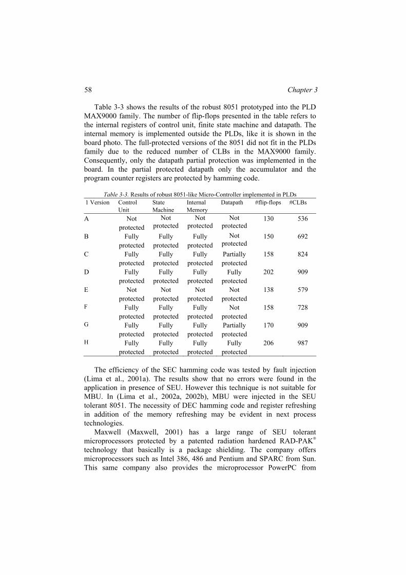
Table 3-3 shows the results of the robust 8051 prototyped into the PLD MAX9000 family. The number of flip-flops presented in the table refers to the internal registers of control unit, finite state machine and datapath. The internal memory is implemented outside the PLDs, like it is shown in the board photo. The full-protected versions of the 8051 did not fit in the PLDs family due to the reduced number of CLBs in the MAX9000 family. Consequently, only the datapath partial protection was implemented in the board. In the partial protected datapath only the accumulator and the program counter registers are protected by hamming code.
Table 3-3. Results of robust 8051-like Micro-Controller implemented in PLDs 1 Version Control
Unit State Machine
Internal Memory
Datapath #flip-flops #CLBs
A Not protected
Not protected
Not protected
Not protected
130 536
B Fully protected
Fully protected
Fully protected
Not protected
150 692
C Fully protected
Fully protected
Fully protected
Partially protected
158 824
D Fully protected
Fully protected
Fully protected
Fully protected
202 909
E Not protected
Not protected
Not protected
Not protected
138 579
F Fully protected
Fully protected
Fully protected
Not protected
158 728
G Fully protected
Fully protected
Fully protected
Partially protected
170 909
H Fully protected
Fully protected
Fully protected
Fully protected
206 987
The efficiency of the SEC hamming code was tested by fault injection
(Lima et al., 2001a). The results show that no errors were found in the application in presence of SEU. However this technique is not suitable for MBU. In (Lima et al., 2002a, 2002b), MBU were injected in the SEU tolerant 8051. The necessity of DEC hamming code and register refreshing in addition of the memory refreshing may be evident in next process technologies.
Maxwell (Maxwell, 2001) has a large range of SEU tolerant microprocessors protected by a patented radiation hardened RAD-PAK® technology that basically is a package shielding. The company offers microprocessors such as Intel 386, 486 and Pentium and SPARC from Sun. This same company also provides the microprocessor PowerPC from

SINGLE EVENT UPSET (SEU) MITIGATION TECHNIQUES 59
Motorola with the CPU protected by TMR and the memory protected by EDAC. The TMR compares the output of each of 3 CPUs on a bit-by-bit basis. In the event of a single upset a simple voting scheme detects and selects the correct value. The advent of a second error would be uncorrectable, thus the processor is flushed and synchronized. In addition the components also have the package shielding.
Honeywell (Honeywell, 2003) offers fault-tolerant microprocessors based on device redundancy and EDAC techniques too. An example is the radiation hardened PowerPC 603, where the data and program memories are protected by SEC-DED hamming code and redundancy is applied in the internal registers. Aitech Defense Systems Inc. (Aitech, 2001) also provides a radiation tolerant PowerPC 750 protected by EDAC.
Lockheed Martin has developed a SEU tolerant PowerPC (G3) for JPL (JPL Laboratory, 2001). It provides a modular standard product that allows the spacecraft developer excellent flexibility in system configuration. There are over 800,000 storage elements in the PowerPC 750 (G3), all of which have been replaced with SEU hardened circuitry in the RAD750. The earlier RAD6000 employed resistor decoupling memory cells (figure 3-18) that require special polysilicon resistors in the manufacturing process. The RAM cells and latches in the RAD750 have been designed using hardening techniques for circuits that require no special process steps and optimize performance using the cells referred to in (Liu and Whitaker, 1992), figure 3-25. The memory and PROM located on the board have been protected by EDAC.
Atmel provides an 8-bit radiation tolerant micro-controller 80C32E, DSP microprocessor and a SPARC microprocessor for military and space applications (Atmel, 2001). The radiation tolerant DSP microprocessor Radiation from Atmel uses the Hit cell (Velazco et al., 1994), figure 3-20, in order to protect the memory cells against radiation. The Atmel SPARC microprocessor is protected by EDAC. The Atmel static RAM design separates the cells that represent the different data word bits. This feature virtually eliminates the risk of one impact provoking dual bit upsets (MBU) leaving only single bit upsets (SEU) that can be corrected by SEC hamming code. The additional processing associated with an EDAC protected solution is the initialization of the check bit RAM and a refresh procedure that performs read-write operations on the protected memory, also called scrubbing. The initialization of the check bit RAM does not introduce an overhead, since most space borne applications move their code from ROM to RAM at reset, and automatically initialize the check bit RAM at the same time. The scrubbing performed during processor idle time is necessary to eliminate the risk of two separate impacts generating a dual bit upset (MBU) in the same data word. However, if a dual bit upset in the same data word

60 Chapter 3
should occur it would still be detected and signaled by the EDAC, SEC-DED hamming code.
In (Gaisler, 2002), a fault-tolerant processor is proposed: the Spacelite, based on the SPARC V8 architecture. The techniques applied to this processor aim to detect and to tolerate one error in any on-chip register, and one error correction and double error detection in two adjacent bits in any on-chip memory structure (caches and tags). The approach to SEU fault-tolerance in the Spacelite processor is to divide all registers into two groups; primary and redundant. A primary register is defined as register carrying information, which is not present anywhere else in the system (processor or memory) and where an error in the register contents would cause a malfunction of the system. A redundant register is defined as a register that contains information that is replicated somewhere else in the system, and can be recreated by either reloading the register or performing other recovery actions. An error in a redundant register must also not alter the state or operation of the system in a way that will create a malfunction during the time it contains an erroneous value. To tolerate one random register error, all primary registers are designed fault-tolerant, either by replication or by use of error-correcting codes. The redundant registers need only be provided with error-detection functions, since they can be recovered from their redundant locations.
Individual fault-tolerant registers are implemented using TMR, three registers in parallel and a voter selecting the majority result. The benefit of such a scheme is that error masking and error-removal is implicit, and than no glitch is produced at the output when a SEU occurs. The register file is provided with a 32-bit single error correction (SEC) and double error detection (DED) EDAC instead of TMR cells to reduce the overhead. Errors in redundant registers are detected through parity generation and checking. Cache memories and tags are protected with two parity bits, one for odd and one for even data bits. This scheme makes it possible to detect a double-error in two adjacent bits. In case of an EDAC error, the corrected register value is written back to the register file when the instruction reaches the write stage, and the instruction is then restarted. An error in the cache memory (instruction or data) will automatically cause a cache miss, and the cache will be updated with the correct data from the main memory.
In (Rebaudengo et al., 2002), the software implemented fault tolerance (SIFT) is discussed to protect microprocessors against upsets in the sequential (SEU) and combinational logic (SET). Fault injection experi-ments have been performed to evaluate the capabilities of the SIFT technique of detecting transient faults in the internal memory elements of a processor and in its combinational logic. The originality of the strategy relies on the fact of being based on a set of simple transformation rules, which can

SINGLE EVENT UPSET (SEU) MITIGATION TECHNIQUES 61
be implemented on any high-level code. This reduces the costs for program hardening. The SIFT system implementations were tested under radiation in the 8051 micro-controller. Results show that SIFT tool was able to detect 88.2% of the upsets observed in the processor. However, this technique needs extra memory as the program code increases.
3.3 EXAMPLES OF SEU MITIGATION TECHNIQUES IN FPGA
Field Programmable Gate Array (FPGA) devices are becoming increasingly popular with spacecraft electronic designers as they fill a critical niche between discrete logic devices and the mask programmed gate arrays. The devices are inherently flexible to meet multiple requirements and offer significant cost and schedule advantages. Since FPGAs are re-programmable, data can be sent after launch to correct errors or improve the performance of spacecraft.
The architecture of programmable logic components is based on an array of logic blocks that can be programmed by the interconnections to implement different designs. A FPGA logic block can be as simple as a small logic gate or as complex as clusters composed of many gates. The logic blocks of current commercial FPGAs are composed of one or more pairs of transistor, small gates, multiplexors, Lookup tables and and-or structures. The routing architecture incorporates wire segments of various lengths, which can be interconnected via electrically programmable switches. Several different programming technologies are used to implement the programmable switches. There are three types of such programmable switch technologies currently in use:
- SRAM, where the programmable switch is a pass transistor controlled
by the state of a SRAM bit (SRAM based FPGAs) - Antifuse, when an electrically programmable switch forms a low
resistance path between two metal layers. (Antifuses based FPGAs) - EPROM, EEPROM or FLASH cell, where the switch is a floating
gate transistor that can be turned off by injecting charge onto the floating gate. These programmable logic circuits are called EPLDs or EEPLDs.
Customizations based on SRAM are volatile. This means that SRAM-
based FPGAs can be reprogrammed as many times as necessary at the work site. The antifuse customizations are non-volatile and they can be pro-grammed just once. Each FPGA has a particular architecture. Programmable
S

62 Chapter 3
logic companies such as Xilinx and Actel offer radiation tolerant FPGA families. Each company uses different mitigation techniques to better take into account the architecture characteristics. Some companies from the space market are licensed to develop tolerant FPGAs, such as Aeroflex UTMC, which is licensed to QuickLogic, and Honeywell, which is licensed to Atmel. However, there is no current, finished space product based on the QuickLogic and Atmel FPGAs so far. Actel and Xilinx are the main commercial FPGA companies to share the market of space FPGAs nowadays as observed in the industry floor of the most important conferences of the area such as Military and Aerospace Applications of Programmable Devices and Technologies (MAPLD), Nuclear and Space Radiation Effect (NSREC), Radiation Effects on Components and Systems (RADECS) and Field Programmable Gate Array Symposium (FPGA).
The programmable logic devices are critically sensitive to SEU due to the large amount of memory elements located in these structures. Programmable logic devices must be strongly protected to avoid errors running in the space environment. There are two main ways to mitigate the radiation effects in Programmable Logic Devices: by high-level description or by architectural design.
Each method has a different implementation cost and it can be more suitable for some types of applications, FPGA topology and customization approach. For example, FPGAs programmed by antifuse topology are more like standard cell ASICs, as the customization cells (antifuse) are not susceptible to radiation effects. For this reason, techniques used in ASICs such as EDAC can be easily applied to the high-level description. At the architectural level, for instance, it is simple to replace all the flip-flops with hardened memory cells. As you will see later in this book, for FPGAs customizable by SRAM, applying high-level SEU mitigation techniques is not so simple because all the design blocks are sensitive to radiation. The same occurs when architecture design techniques are applied because of the FPGA matrix complexity.
3.3.1 Antifuse based FPGAs
The problem of SEU in antifuse FPGAs, more specifically based on the Actel architecture, has been addressed in (Katz et al., 1997, 1998, 1999; Wang et al., 2000). Actel started offering SEU tolerant FPGA families programmed by antifuse called SX some years ago (Actel, 2000). This family architecture is described as a “sea-of-modules” architecture, because the entire floor of the device is covered with a grid of logic modules with virtually no chip area lost to interconnect elements or routing. Actel’s SX family has been improved in the past years. The first version provided two

SINGLE EVENT UPSET (SEU) MITIGATION TECHNIQUES 63
types of logic modules, identical to the standard Actel family, the register cell (R-cell) and the combinatorial cell (C-cell) exemplified in figure 3-31.
D00D01D10D11
S1 S0
Y
D00D01D10D11
S1 S0
YCLR
CLKOUT
(a) Combinational ACT1 (C-cell) and sequential ACT1 (R-cell)
D0D1
D2D3
DB
Y
A0 B0 S1
(b) C-cell represented in detail

64 Chapter 3
/clk clk
D Q
(c) R-cell: Latch representation
Figure 3-31. Architecture of Actel FPGAs
Interconnection between these logic modules is achieved using Actel’s patented metal-to-metal programmable antifuse interconnect elements, which are embedded between the metal 2 and metal 3 layers. These antifuses are normally open circuit and, when programmed, form a permanent low-impedance connection. In this first SEU tolerant FPGA version (Actel, 2001), three proposed techniques for implementing the logic of the sequential elements in order to avoid upsets were presented: CC, TMR, or TMR_CC. The sequential elements are automatically implemented during the synthesis in the Symplify tool. The CC technique uses combinatorial cells with feedback instead of flip-flop or latch primitives to implement storage cells. For example, a DFP1, comprised of two combinational modules, would be used in place of a DF1. This technique can avoid SEU in CMOS technologies larger than 0.23 µm but it will not be able to avoid SEU in next-generation process technologies where the combinational logic can also be affected by charged particles. TMR is a register implementation technique where each register is implemented by three flip-flops or latches that “vote” to determine the state of the register. TMR_CC is also a triple-module-redundancy technique, where each voting register is composed of combinatorial cells with feedback (instead of flip-flop or latch primitives).
The CC flip-flops (CC-FFs) produce designs that are more resistant to SEU effects than designs that use the standard flip-flop (S-FF). CC-FFs typically use twice the area resources of S-FFs. Triple voting, or triple module redundancy (TMR), produces designs that are most resistant to SEU effects. Instead of a single flip-flop, triple voting uses three flip-flops leading to a majority gate voting circuit. This way, if one flip-flop is flipped to the wrong state, the other two would override it, and the correct value is propagated to the rest of the circuit. Because of the cost (three to four times the area and two times the delay required for S-FF implementations), triple voting is usually implemented using S-FFs. However, one can implement triple voting using only CC-FFs in the Synplify tool.

SINGLE EVENT UPSET (SEU) MITIGATION TECHNIQUES 65
Currently, Actel offers the RTFXS and RTAXS FPGA families (Radiation Tolerant FX or AX architecture “Space” versions). These devices use metal-to-metal antifuse connections for configuration and include built-in TMR on all registers. These new SEU-hardened structures eliminate the need for TMR flip-flop designs implemented in HDL because the flip-flop is already protected by TMR at the architectural level (matrix). They use the D-type flip-flop proposed in (Katz et al., 2001; Wang et al., 2003), figure 3-32. Three D-type flip-flops are connected in parallel to the clock and data inputs. A voter (or majority circuit) is implemented by the top MUX to create a “hardened” output. The outputs of two flip-flops, A and B, go to the selects of the voter MUX. If both A and B read logic zero, MUX input D0 is selected. Since it is tied to GND, the output of the MUX will read logic zero. Similarly, if A and B read logic one, the output of the MUX will read logic one. If A and B disagree due to a SEU (or for other reasons), the MUX will select flip-flop C. We know C agrees with either A or B, and thus the MUX “voted” to produce data agreed on by two of the three flip-flops.
AA
B
C
BA
B
C
CA
B
C
Q
D
G
Figure 3-32. Built-in TMR on a memory cell in the Radiation Tolerant FX or AX architecture
Actel’s FPGAs
3.3.2 SRAM-based FPGAs
The SEU has a peculiar effect in SRAM-based FPGAs, as discussed in the previous chapter. As a consequence, it is not that simple to apply a high-level technique to this type of FPGAs, because all the implementation blocks

66 Chapter 3
(logic, customization and routing) are susceptible to upsets. Many solutions in the literature suggest new architecture topologies for SRAM-based FPGAs using hardened memory cells and innovative routing structures. Others solutions are high-level description techniques developed to be applied on the most popular family of SRAM-based FPGA, the Virtex® from Xilinx. The majority of the solutions for Virtex® are based on fault recovery, and they use partial reconfiguration and re-routing to correct upset and guarantee reliability. However, it is important to notice that many of the solutions that have been proposed for the Virtex® FPGA family in the high-level description are not very efficient because they do not take into account the peculiar effect of a SEU in the SRAM-based FPGA matrix, which is a permanent fault in the logic, customization and routing. Hardware redun-dancy is mandatory in this case to guarantee reliability.
3.3.2.1 SEU Mitigation Solution in high-level description
Xilinx has a military family for the Virtex® that is also used for space applications. Xilinx present many FPGA families for space applications. They are called QPro and it provides a commercial off-the-shelf system-level solution for aerospace and defense customers. It started with Virtex® QPRO family (Xilinx, 2000), which is fabricated on thin-epitaxial silicon wafers using the commercial mask set and the Xilinx 5-layer-metal 0.22 µm CMOS process. The use of epitaxial CMOS process technology has made Virtex® Single Event latchup immune (LETth >120 MeV*cm2/mg, TID = 100 Krads(si)). Currently, Xilinx’s Virtex®II QPro family, popular in space use, includes the same features as the regular Virtex®II Pro (integrated Power PC core, integrated SERDES, etc.) and is adapted for space use with extended temperature ranges, extended radiation tolerance, and ceramic packages.
In addition, Xilinx has proposed a high-level technique to mitigate SEU in the SRAM-based FPGA: the TMR approach in the high-level design description combined to reconfiguration (scrubbing) in order to avoid accumulation of upsets (Carmichael et al., 2000, 2001). This solution is complete to avoid single points of failure in the matrix as all blocks are triplicated. This solution has been investigated and experiment tests were performed. In the chapters 5, 6 and 7 the SEU mitigation technique based on TMR for the Virtex® FPGA from Xilinx is discussed in detail.
In (Alderighi et al., 2002), a design for a Xilinx FPGA-based multistage interconnection network (MIN) for a multi-sensor system that will be used in future scientific space missions is proposed. It is characterized by good concurrent fault diagnosis and fault detection capabilities. The fault tolerance strategy adopted is based on both network configuration and FPGA re-configuration. A slice control unit, one per each slice, allows changing the

SINGLE EVENT UPSET (SEU) MITIGATION TECHNIQUES 67
actual slice configuration, while the network control unit sets a new permutation. When a fault affecting a slice is detected, a finite-state machine fires and marks the actual configuration as faulty in the LUT with a fault. The state machine goes, in turn, to an active status and searches for an equivalent configuration available among those stored in the configuration LUT. When such a configuration is found, it is applied to fix the problem. To detect faults, a parity checker is used in each slice. Parity is actually the only invariant property that can be defined for the slice. The parity checker is endowed with self-checking ability, so that it can report faulty conditions relevant to the set of faults.
The limitation of this method is that only very few types of faults can be recovered by reconfiguring the network. All the faults in the customization routing in the FPGA that have permanent effect (as described in previous chapter) can only be corrected by FPGA reconfiguration (scrubbing). Results show that only 10% of the injected single upsets are recovered by the method, which are probably the faults in the LUTs. The majority are recovered by simple scrubbing.
3.3.2.2 SEU Mitigation Solutions at the Architectural level
In (Mavis et al., 1998), a FPGA has been developed for space and military applications based on a combination of four technologies: (1) radiation hardened nonvolatile SONOS (Silicon-Oxide Nitride-Oxide Semiconductor) EEPROM transistors, (2) unique SEU immune storage circuits, both for nonvolatile SONOS implementations and for volatile SRAM (static random access memory) implementations, (3) high-performance, radiation hardened, 0.8 µm, 3-level metal CMOS technology, and (4) new FPGA architectures developed specifically to accommodate good radiation-hardened circuit design practices. It is hardened for total ionization dose up to 200 krad(Si) and LET greater than 100 MeV-cm2/mg. The NMOS SONOS transistors differ from conventional NMOS transistors in that the SONOS transistor has a variable threshold voltage while the NMOS transistor has a fixed threshold voltage. To erase a SONOS transistor (program it to a negative threshold voltage) a large (10 V) negative voltage is applied from the gate to the P-Well. This causes pair-hole tunneling into the nitride-oxide gate dielectric layer, and the resulting positive charge storage produces a depletion mode device. To store data in the transistor (program it to a positive threshold voltage) a large (10 V) positive voltage is applied from the gate to the P-Well. This causes electron tunneling into the gate dielectric and the resulting negative stored charge. In the SRAM version of the FPGA, volatile configuration storage is accomplished using a circuit derived from the DICE (dual interlocked storage cell) latch. The chip is

68 Chapter 3
programmed in much the same way as the SONOS version, using a shift register to serially load the row data and a column decode to select the column being written.
Actel has prototyped an SRAM-based FPGA (Wang et al., 1999). In this case, the standard SRAM memory cells were replaced by resistor-decoupling memory cells where the effectiveness depends on the resistor value; and DICE memory cells that are practically SEU immune at 0.25µm if only one node is hit. Figure 3-18 demonstrates the resistor decoupling memory cell and figure 3-23 the DICE cell, respectively. The resistor decoupling memory cell is able to avoid upsets because the resistors inserted in the feedback path work as filters to the transient pulse provoked by the charged particle. The DICE cell can avoid upsets because it stores data in two distinct parts, where if one part is corrupted the other one is isolated by the cell construction. However, conclusions presented in (Wang et al., 1999) show that multiple bit upsets (MBU) will limit both solutions in the future if the layout does not pay special attention to this issue. The redundancy hardening (DICE memory) is less effective than the resistor solution in two orders of magnitude regarding upset rates. The disadvantage of the resistor solution is temperature operation range sensitivity and the delay increase. The DICE also has a disadvantage in area overhead. It has 12 transistors compared to 6 transistors in the standard memory cell. For 0.18µm, the effectiveness of both solutions will be compromised and more ingenious designs will be needed in the circuit level.
Atmel (Atmel, 2001) also has published a version of an SRAM-based FPGA (AT6010) using the SOI process. The original logic block was not logically modified. The improvement achieved is limited to the SOI reliability in presence of SEU. Previous results have shown that the use of only SOI technology does not guarantee protection against SEU. Conse-quently, this solution from Atmel is not completely suitable for the space environment.
In (Kumar, 2003), a new SRAM-based FPGA is proposed based on the human immune system. This architecture adopts a distributed network without any centralized control. Error (antigen) detection is based on the principle of operation of the B-cell. Once an error is detected in a functional cell, a pre-determined spare cell replaces the functional cell by cloning its behavior. The proposed reconfiguration technique reduces the redundancy in the system.
Functional cells consist of a 10-bit control register, 1-bit error register and a logic block. The contents of the control register may be considered as the genetic code. The process of recognizing an error (antigen) by a B-cell is emulated in a functional cell by ensuring that the outputs generated are complementary. If the outputs are identical i.e. an error is present, the results

SINGLE EVENT UPSET (SEU) MITIGATION TECHNIQUES 69
are forced into high impedance. By forcing the outputs of a functional cell to 00 or 11 in the presence of an error, the role of a B cell is emulated. Once an error has been detected the 1-bit error register in the cell is set to 1, and all input information of the functional cell is loaded into the corresponding spare cell. The same occurs in the routing cell that also has a control register to detect the presence of faults. The authors did not go into much detail about faults in the control registers and how much time the system must be on hold until the logic is replaced by the spare logic.
3.3.2.3 Recovery technique
Many fault-tolerant approaches for SRAM-based FPGAs were presented in the past years related to re-routing and alternate configuration to avoid upsets in the used CLBs. The first problem of correcting faults by runtime reconfiguration without using any redundancy is the method to find the faults in the matrix. In (Mitra et al., 1998), a method that uses pseudo-exhaustive BIST is presented to detect upsets in the matrix. The technique has an extra advantage that it is not necessary to bring the whole system down while fault location is carried out. The problem is the time duration to detect faults. Some applications can not be on hold for a long time waiting for the system to be recovered.
An example of fault recovery based on reconfiguration and re-routing is shown in (Lach et al., 1998, 2000), where the physical design is partitioned into a set of tiles. The key element of this approach is partially reconfiguring the FPGA to an alternate configuration in response to a fault. If the new configuration implements the same function as the original, while avoiding the faulty hardware block, the system can be restarted. The challenging step is to identify an alternate configuration efficiently and to have fast runtime fault detection. In (Xu et al., 2000), another fault-tolerant approach for SRAM-Based FPGAs is presented related to the routing procedure. The problem is that both papers discuss radiation effects that are mainly upset (SEU). But in this case, the fault will be corrected in the next load of the bitstream (reconfiguration) and no work must be done in searching a new alternate configuration or routing. The methods are only justified if real permanent faults are present in the matrix due to total ionization dose, such as gate rupture, short or open metal wires.
In (Yu and Mccluskey, 2001), a solution to permanent fault repair in finer granularity of the FPGA is presented. A faulty module can be repaired by reconfiguring the chip so that a damaged configurable logic block (CLB) or routing resource is not used by the design. Many techniques have been presented to provide permanent fault removal for FPGAs through recon-figuration. One approach is to generate a new configuration after permanent

70 Chapter 3
faults are detected in computing systems. Another approach is to generate pre-compiled alternative FPGA configurations and store the configuration bit maps in non-volatile memory, so that when permanent faults are present, a new configuration can be chosen without the delay of re-routing and re-mapping. The authors propose some equivalent design candidates that can replace the original TMR design in case of a permanent fault, figure 3-33.
A B
voterA B
A B
M0
M1
M2
A
BvoterA
A
M0
M1
M2 CED
(a) (b)
A B
A B
A
M1
M2
=
voter
M0
A B
A BM1
=
M0
CED
CED
error0
error1
(c) (d)
Figure 3-33. Design candidates modified from TMR. (a) The original TMR design. (b) A hybrid TMR-Simplex-CED design. (c) A duplex system with a checking block. (d) A duplex
system with two CED blocks (YU and MCCLUSKEY, 2001)
For system transients, the authors suggest the use of traditional transient error recovery techniques. Typical examples include the roll-forward and rollback recovery techniques. Basically, these approaches are designed at the system level and thus are general to recover both Application Specific Integrated Circuit (ASIC) and FPGA systems. However, this assumption is

SINGLE EVENT UPSET (SEU) MITIGATION TECHNIQUES 71
not true, because in the SRAM-based FPGA not only can the logic be affected by upsets, but also the routing, which can invalidate the path to perform roll-forward and rollback techniques. The paper does not discuss the difference between real permanent faults (gate rupture, open or short metal wires) and the SEU that also has a permanent effect until the next reconfiguration.
In (Huang and Mccluskey, 2001), partial reconfiguration is also discussed to improve reliability by detecting and correcting errors in on-chip configuration data, but another problem is addressed in this paper: the memory coherence capability during partial reconfiguration. Because the LUTs can also implement memory modules for user applications, a memory coherence issue arises such that memory contents in user applications may be altered by the online configuration data recovery process. In this reference, the memory coherence problem is investigated, and it is proposed a memory coherence technique that does not impose extra constraints on the placement of memory-configured LUTs. Theoretical analyses and simulation results show that the proposed technique guarantees the memory coherence with a very small (on the order of 0.1%) execution time overhead in user applications. This technique is interesting and it can be further used with FPGA scrubbing in order to avoid SEU in the embedded memory too.
In summary, many fault-tolerant techniques have been proposed over the last years for SRAM-based FPGAs based on recovery, architectural design and high-level design. The majority of the techniques proposed in the past related to the high-level design method and the recovery procedure do not take into account all the details and effects of a SEU in the SRAM-based FPGA because this knowledge is very recent. No published paper before (Lima et al., 2003a) has established the difference between a real permanent fault and a SEU that has also a permanent effect in the LUTs, customization and routing cells in the FPGA. The next chapters show in detail the analysis of the effects of a SEU in the programmable matrix and the importance of using some kind of redundancy in order to ensure run time error recovery and scrubbing (continuous reconfiguration) to avoid accumulation of faults.