Chapter 3 – The Heritage of the IBM System/360 3 – The Heritage of the IBM System/360 ......
30
S/370 Assembler Language Heritage of the S/360 Page 38 Chapter 3 Last Revised on November 5, 2008 Copyright © 2009 by Edward L. Bosworth, Ph.D. Chapter 3 – The Heritage of the IBM System/360 The IBM System/360 was announced on April 7, 1964. It is considered to be either an early third–generation computer or a hybrid of the second generation and third generation. The goals of this chapter include the following: 1. To understand the events that lead to the development of the System/360 family of computers and the context into which this family must fit. 2. To understand the motivation for IBM’s creation of a family of computers, with identical architecture, spanning a wide range of performance capabilities. 3. To define the standard five generations of computing technology, relating each generation to the underlying circuitry and giving examples of each. We begin this chapter by addressing the last goal. In order to place the System/360 family correctly, we must study the technologies leading up to it. The standard division lists five generations, numbered 1 through 5. Here is one such list, taken from the book Computer Structures: Principles and Examples [R04]. 1. The first generation (1945 – 1958) is that of vacuum tubes. 2. The second generation (1958 – 1966) is that of discrete transistors. 3. The third generation (1966 – 1972) is that of small-scale and medium-scale integrated circuits. 4. The fourth generation (1972 – 1978) is that of large-scale integrated circuits.. 5. The fifth generation (1978 onward) is that of very-large-scale integrated circuits. This classification scheme is well established and quite useful, but does have its drawbacks. Two that are worth mention are the following. 1. The term “fifth generation” has yet to be defined in a uniformly accepted way. For many, we continue to live with fourth–generation computers and are even now looking forward to the next great development that will usher in the fifth generation. 2. This scheme ignores all work before the introduction of the ENIAC in 1945. To quote an early architecture book, much is ignored by this ‘first generation’ label. “It is a measure of American industry’s generally ahistorical view of things that the title of ‘first generation’ has been allowed to be attached to a collection of machines that were some generations removed from the beginning by any reasonable accounting. Mechanical and electromechanical computers existed prior to electronic ones. Furthermore, they were the functional equivalents of electronic computers and were realized to be such.” [R04, page 35] The IBM System/360, which is the topic of this textbook, was produced by the International Business Machines Corporation. By 1952, when IBM introduced its first electronic computer, it had accumulated over 50 years experience with tabulating machines and electromechanical computers. In your author’s opinion, this early experience greatly affected the development of all IBM computers; for this reason it is studied.
Transcript of Chapter 3 – The Heritage of the IBM System/360 3 – The Heritage of the IBM System/360 ......

S/370 Assembler Language Heritage of the S/360
Page 38 Chapter 3 Last Revised on November 5, 2008Copyright © 2009 by Edward L. Bosworth, Ph.D.
Chapter 3 – The Heritage of the IBM System/360
The IBM System/360 was announced on April 7, 1964. It is considered to be either an earlythird–generation computer or a hybrid of the second generation and third generation. Thegoals of this chapter include the following:
1. To understand the events that lead to the development of the System/360 familyof computers and the context into which this family must fit.
2. To understand the motivation for IBM’s creation of a family of computers, withidentical architecture, spanning a wide range of performance capabilities.
3. To define the standard five generations of computing technology, relating eachgeneration to the underlying circuitry and giving examples of each.
We begin this chapter by addressing the last goal. In order to place the System/360 familycorrectly, we must study the technologies leading up to it.
The standard division lists five generations, numbered 1 through 5. Here is one such list,taken from the book Computer Structures: Principles and Examples [R04].
1. The first generation (1945 – 1958) is that of vacuum tubes.2. The second generation (1958 – 1966) is that of discrete transistors.3. The third generation (1966 – 1972) is that of small-scale and medium-scale
integrated circuits.4. The fourth generation (1972 – 1978) is that of large-scale integrated circuits..5. The fifth generation (1978 onward) is that of very-large-scale integrated circuits.
This classification scheme is well established and quite useful, but does have its drawbacks.Two that are worth mention are the following.
1. The term “fifth generation” has yet to be defined in a uniformly accepted way.For many, we continue to live with fourth–generation computers and are even nowlooking forward to the next great development that will usher in the fifth generation.
2. This scheme ignores all work before the introduction of the ENIAC in 1945. To quotean early architecture book, much is ignored by this ‘first generation’ label.
“It is a measure of American industry’s generally ahistorical view of things that thetitle of ‘first generation’ has been allowed to be attached to a collection of machinesthat were some generations removed from the beginning by any reasonableaccounting. Mechanical and electromechanical computers existed prior to electronicones. Furthermore, they were the functional equivalents of electronic computers andwere realized to be such.” [R04, page 35]
The IBM System/360, which is the topic of this textbook, was produced by the InternationalBusiness Machines Corporation. By 1952, when IBM introduced its first electronic computer,it had accumulated over 50 years experience with tabulating machines and electromechanicalcomputers. In your author’s opinion, this early experience greatly affected the developmentof all IBM computers; for this reason it is studied.

S/370 Assembler Language Heritage of the S/360
Page 39 Chapter 3 Last Revised on November 5, 2008Copyright © 2009 by Edward L. Bosworth, Ph.D.
A Revised Listing of the GenerationsWe now present the classification scheme to be used in this textbook. In order to fit thestandard numbering scheme, we follow established practice and begin with “Generation 0”.
Generation 0 (1642 through 1945)This is the era of purely mechanical calculators and electromechanical calculators. At thistime the term “computer” was a job title, indicating a human who used a calculating machine.
Generation 1 (1945 through 1958)This is the era of computers (now defined as machines) based on vacuum tube technology.
All subsequent generations of computers are based on the transistor, which was developed byBell Labs in late 1947 and early 1948. It can be claimed that each of the generations thatfollow represent only a different way to package transistors. Of course, one can also claimthat a modern F–18 is just another 1910’s era fighter. Much has changed.
Generation 2 (1958 through 1966)Bell Labs licensed the technology for transistor fabrication in late 1951 and presented theTransistor Technology Symposium in April 1952. The TX–0, an early experimentalcomputer based on transistors, it became operational in 1956. IBM’s first transistor–basedcomputer, the 7070, was announced in September 1958.
Generation 3 (1966 through 1972)This is the era of SSI (Small Scale Integrated) and MSI (Medium Scale Integrated) circuits.Each of these technologies allowed the placement of a number of transistors on a single chipfabricated from silicon, with the wiring between the transistors being achieved by lines ofaluminum actually etched on the chip. There were no large wires on the chip.
SSI corresponded to 100 or fewer electronic components on a chip.
MSI corresponded to between 100 and 3,000 electronic components on a chip.
Generation 4 (1972 – 1978)This is the era of LSI (Large Scale Integrated) chips, with up to 100,000 components on thechip. Many of the early Intel processors fall into this generation.
Generation 4 B (1978 and later)This is the era of VLSI (Very Large Scale Integrated) chips, having more than 100,000components on the chip. The Intel Pentium series belongs here.
This textbook will not refer to any computing technology as “fifth generation”; the term is justtoo vague and has too many disparate meanings. As a matter of fact, it will not make manyreferences to the fourth generation, as the IBM System/360 family is definitely thirdgeneration or earlier.
A Study of SwitchesAll stored program computers are based on the binary number system, implemented usingsome sort of switch that turns voltages on and off. The history of the computer generations isprecisely a history of the devices used as voltage switches. It begins with electromechanicalrelays and continues through vacuum tubes and transistors. Each of the latter two has manyuses in analog electronics; the digital use is a rather specialized modification of the operatingregime that causes each to operate as a switch.

S/370 Assembler Language Heritage of the S/360
Page 40 Chapter 3 Last Revised on November 5, 2008Copyright © 2009 by Edward L. Bosworth, Ph.D.
Electronic RelaysElectronic relays are devices that use (often small) voltages to switch other voltages. Oneexample of such a power relay is the horn relay found in all modern automobiles. A smallvoltage line connects the horn switch on the steering wheel to the relay under the hood. Thatrelay switches a high–current line that activates the horn.
The following figure illustrates the operation of an electromechanical relay. The iron coreacts as an electromagnet. When the core is activated, the pivoted iron armature is drawntowards the magnet, raising the lower contact in the relay until it touches the upper contact,thereby completing a circuit. Thus electromechanical relays are switches.
Figure: An Electromechanical Relay
In general, an electromechanical relay is a device that uses an electronic voltage to activate anelectromagnet that will pull an electronic switch from one position to another, thus affectingthe flow of another voltage; thereby turning the device “off” or “on”. Relays display theessential characteristic of a binary device – two distinct states. Below we see pictures of tworecent-vintage electromechanical relays.
Figure: Two Relays (Source http://en.wikipedia.org/wiki/Relay)

S/370 Assembler Language Heritage of the S/360
Page 41 Chapter 3 Last Revised on November 5, 2008Copyright © 2009 by Edward L. Bosworth, Ph.D.
The primary difference between the two types of relays shown above is the amount of powerbeing switched. The relays for use in general electronics tend to be smaller and encased inplastic housing for protection from the environment, as they do not have to dissipate a largeamount of heat. Again, think of an electromechanical relay as an electronically operatedswitch, with two possible states: ON or OFF.
Power relays, such as the horn relay, function mainly to isolate the high currents associatedwith the switched apparatus from the device or human initiating the action. One common useis seen in electronic process control, in which the relays isolate the electronics that computethe action from the voltage swings found in the large machines being controlled.
In use for computers, relays are just switches that can be operated electronically. Tounderstand their operation, the student should consider the following simple circuits.
Figure: Relay Is Closed: Light Is Illuminated
Figure: Relay Is Opened: Light Is Dark.
We may use these simple components to generate the basic Boolean functions, and from thesethe more complex functions used in a digital computer. The following relay circuitimplements the Boolean AND function, which is TRUE if and only if both inputs are TRUE.Here, the light is illuminated if and only if both relays are closed.
Figure: One Closed and One Open
Computers based on electromagnetic relays played an important part in the early developmentof computers, but became quickly obsolete when designs using vacuum tubes (considered aspurely electronic relays) were introduced in the late 1940’s. These electronic tubes also hadtwo states, but could be switched more quickly as there were no mechanical components to bemoved.

S/370 Assembler Language Heritage of the S/360
Page 42 Chapter 3 Last Revised on November 5, 2008Copyright © 2009 by Edward L. Bosworth, Ph.D.
Vacuum TubesThe next step in digital logic was the use of a vacuum tube as a digital switch. As this devicewas purely electrical, it was much faster than the electromechanical relays that had been usedin digital computing machines prior to about 1945. The figure below shows four vacuumtubes from this author’s personal collection. Note that the big one is about 5 inches tall.
Figure: Four Vacuum Tubes Mounted in Styrofoam
The big vacuum tube to the right is a diode, which is an element with 3 major components: afilament, a cathode and a grid. This would have been used as a rectifier as a part of a circuitto convert AC (Alternating Current) into DC (Direct Current).
The cathode is the element that is the source of electrons in the tube. When it is heated eitherdirectly (as a filament in a light bulb) or indirectly by a separate filament, it will emitelectrons, which either are reabsorbed by the cathode or travel to the anode. When the anodeis held at a voltage more positive than the cathode, the electrons tend to flow from cathode toanode (and the current is said to flow from anode to cathode – a definition made in the early19th century before electrons were understood). The anode is the silver “cap” at the top.
One of the smaller tubes is a triode, which has four major components: the above three as wellas a controlling grid placed between the cathode and the anode. This serves as a currentswitch, basically an all–electronic relay. The grid serves as an adjustable barrier to theelectrons. When the grid is more positive, more electrons tend to leave the cathode and fly tothe anode. When the grid is more negative, the electrons tend to stay at the cathode. By thismechanism, a small voltage change applied to the grid can cause a larger voltage change inthe output of the triode; hence it is an amplifier. As a digital device, the grid in the tube eitherallows a large current flow or almost completely blocks it – “on” or “off”.
Here we should add a note related to analog audio devices, such as high–fidelity and stereoradios and record players. Note the reference to a small voltage change in the input of a tubecausing a larger voltage change in the output; this is amplification, and tubes were once usedin amplifiers for audio devices. The use of tubes as digital devices is just a special case,making use of the extremes of the range and avoiding the “linear range” of amplification.

S/370 Assembler Language Heritage of the S/360
Page 43 Chapter 3 Last Revised on November 5, 2008Copyright © 2009 by Edward L. Bosworth, Ph.D.
We close this section with a picture taken from the IBM 701 computer, a computer from 1952developed by the IBM Poughkeepsie Laboratory. This was the first IBM computer that reliedon vacuum tubes as the basic technology.
Figure: A Block of Tubes from the IBM 701Source: [R23]
The reader will note that, though there is no scale on this drawing, the tubes appear rathersmall, and are probably about one inch in height. The components that resemble smallcylinders are resistors; those that resemble pancakes are capacitors.
Another feature of the figure above that is worth note is the fact that the vacuum tubes aregrouped together in a single component. The use of such components probably simplifiedmaintenance of the computer; just pull the component, replace it with a functioning copy, andrepair the original at leisure.
There are two major difficulties with computers fabricated from vacuum tubes, each of whicharises from the difficulty of working with so many vacuum tubes. Suppose a computer thatuses 20,000 vacuum tubes; this being only slightly larger than the actual ENIAC.
A vacuum tube requires a hot filament in order to function. In this it is similar to a modernlight bulb that emits light due to a heated filament. Suppose that each of our tubes requiresonly five watts of electricity to keep its filament hot and the tube functioning. The totalpower requirement for the computer is then 100,000 watts or 100 kilowatts.
We also realize the problem of reliability of such a large collection of tubes. Suppose thateach of the tubes has a probability of 99.999% of operating one hour. This can be written as adecimal number as 0.99999 = 1.0 – 10-5. The probability that all 20,000 tubes will beoperational for more than an hour can be computed as (1.0 – 10-5)20000, which can beapproximated as 1.0 – 2000010-5 = 1.0 – 0.2 = 0.8. There is an 80% chance the computerwill function for one hour and 64% chance for two hours of operation. This is not good.
S/370 Assembler Language Heritage of the S/360
Page 44 Chapter 3 Last Revised on November 5, 2008Copyright © 2009 by Edward L. Bosworth, Ph.D.
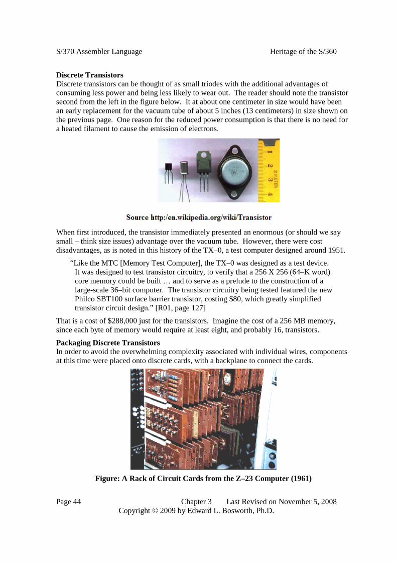
Discrete TransistorsDiscrete transistors can be thought of as small triodes with the additional advantages ofconsuming less power and being less likely to wear out. The reader should note the transistorsecond from the left in the figure below. It at about one centimeter in size would have beenan early replacement for the vacuum tube of about 5 inches (13 centimeters) in size shown onthe previous page. One reason for the reduced power consumption is that there is no need fora heated filament to cause the emission of electrons.
When first introduced, the transistor immediately presented an enormous (or should we saysmall – think size issues) advantage over the vacuum tube. However, there were costdisadvantages, as is noted in this history of the TX–0, a test computer designed around 1951.
“Like the MTC [Memory Test Computer], the TX–0 was designed as a test device.It was designed to test transistor circuitry, to verify that a 256 X 256 (64–K word)core memory could be built … and to serve as a prelude to the construction of alarge-scale 36–bit computer. The transistor circuitry being tested featured the newPhilco SBT100 surface barrier transistor, costing $80, which greatly simplifiedtransistor circuit design.” [R01, page 127]
That is a cost of $288,000 just for the transistors. Imagine the cost of a 256 MB memory,since each byte of memory would require at least eight, and probably 16, transistors.
Packaging Discrete TransistorsIn order to avoid the overwhelming complexity associated with individual wires, componentsat this time were placed onto discrete cards, with a backplane to connect the cards.
Figure: A Rack of Circuit Cards from the Z–23 Computer (1961)

S/370 Assembler Language Heritage of the S/360
Page 45 Chapter 3 Last Revised on November 5, 2008Copyright © 2009 by Edward L. Bosworth, Ph.D.
The interesting features of these cards are illustrated in the figure below, which is a modulecalled a “Flip Chip”. It was used on a PDP–8 marketed by the Digital Equipment Corporationin the late 1960’s. Note the edge connectors that would plug into a wired backplane. Alsonote the “silver” traces on the back of the card. These traces served as wires to connect thecomponents that were on the chip. An identical technology, on a very much smaller scale, hasbeen employed by each of the generations of integrated chips.
Figure: Front and Back of an R205b Flip-Chip (Dual Flip-Flop) [R42]
In the above figure, one can easily spot many of the discrete components. The orangepancake-like items are capacitors, the cylindrical devices with colorful stripes are resistorswith the color coding indicating their rating and tolerances, the black “hats” in the columnsecond from the left are transistors, and the other items must be something useful. The size ofthis module is indicated by the orange plastic handle, which is fitted to a human hand.
It was soon realized that assembly of a large computer from discrete components would bealmost impossible, as fabricating such a large assembly of components without a single faultyconnection or component would be extremely costly. This problem became known as the“tyranny of numbers”. Two teams independently sought solutions to this problem. One teamat Texas Instruments was headed by Jack Kilby, an engineer with a background in ceramic-based silk screen circuit boards and transistor-based hearing aids. The other team was headedby research engineer Robert Noyce, a co-founder of Fairchild Semiconductor Corporation. In1959, each team applied for a patent on essentially the same circuitry, Texas Instrumentsreceiving U.S. patent #3,138,743 for miniaturized electronic circuits, and Fairchild receivingU.S. patent #2,981,877 for a silicon-based integrated circuit. After several years of legalbattles, the two companies agreed to cross-license their technologies, and the rest is history(and a lot of profit).

S/370 Assembler Language Heritage of the S/360
Page 46 Chapter 3 Last Revised on November 5, 2008Copyright © 2009 by Edward L. Bosworth, Ph.D.
Integrated CircuitsIntegrated circuits are nothing more or less than a very efficient packaging of transistors andother circuit elements. The term “discrete transistors” implied that the circuit was built fromtransistors connected by wires, all of which could be easily seen and handled by humans.
As noted above, the integrated circuit was independently developed by two teams ofengineers in 1959. The advantages of such circuits quickly became obvious and applicationsin the computer world soon appeared. We list a few of the more obvious advantages.
1. The integrate circuit solved the “tyranny of numbers” problem mentioned above.More of the wiring connections were placed on the chip of the integrated circuit,which could be automatically fabricated. This automation of production lead todecreased costs and increased reliability.
2. The length of wires interconnecting the integrated circuits was decreased, allowingfor much faster circuitry. In the Cray–1, a supercomputer build with generation 2technologies, the longest wire was 4 feet. Electricity travels on wires at about twofeet per nanosecond; the Cray–1 had to allow for 4 nanosecond round trip times.This limited the maximum clock frequency to about 200 MHz.
The first integrated circuits were classified as SSI (Small-Scale Integration) in that theycontained only a few tens of transistors. The first commercial uses of these circuits were inthe Minuteman missile project and the Apollo program. It is generally conceded that theApollo program motivated the technology, while the Minuteman program forced it into massproduction, reducing the costs from about $1,000 per circuit in 1960 to $25 per circuit in1963. Were such components fabricated today, they would cost less than a penny.
Large Scale and Very Large Scale Integrated Circuits (from 1972 onward)As we shall se, the use of SSI (Small Scale Integration) in the early System/360 modelsyielded an impressive jump in circuit density. We now have a choice: stop here because wehave developed the technology to explain the System/360 and System /370, or trace the laterevolution of the S/360 family through the S/370 (announced in 1970), the 370/XA (1983), theESA/370 (1988), the ESA/390 (1990), and the z/Series (announced in 2000).
The major factor driving the development of smaller and more powerful computers was andcontinues to be the method for manufacture of the chips. This is called “photolithography”,which uses light to transmit a pattern from a photomask to a light–sensitive chemical called“photoresist” that is covering the surface of the chip. This process, along with chemicaltreatment of the chip surface, results in the deposition of the desired circuits on the chip.
In a very real sense, the development of what might be called “Post Generation 3” circuitryreally depended on the development of the automated machinery used to produce thosecircuits. These machines, together with the special buildings required to house them, arecalled “Fabs”, or chip fabrication centers. These fabs are also extraordinarily expensive,costing on the order of $ 1 billion dollars. All of this development is in the future for thecomputers in which we are interested for this course.
We shall limit our thoughts to the first three generations of computer technologies.

S/370 Assembler Language Heritage of the S/360
Page 47 Chapter 3 Last Revised on November 5, 2008Copyright © 2009 by Edward L. Bosworth, Ph.D.
It seems that pictures are the best way to illustrate the evolution of the first three generationsof computer components. Below, we see a picture of an IBM engineer (they all wore coatsand ties at that time) with three generations of components. He is seen sitting in front of thecontrol panel for one of the System/360 models.
The first generation unit (vacuum tubes) is a pluggable module from the IBM 650. Recall thatthe idea of pluggable modules dates to the ENIAC; the design facilitates maintenance.
The second generation unit (discrete transistors) is a module from the IBM 7090.
The third generation unit is the ACPX module used on the IBM 360/91 (1964). Each chip wascreated by stacking layers of silicon on a ceramic substrate; it accommodated over twentytransistors. The chips could be packaged together onto a circuit board. Note the pencilpointing to one of the chips on the board. It is likely that this chip has functionality equivalentto the transistorized board on the right or the vacuum tube pluggable unit on the left.
Figure: IBM Engineer with Three Generations of Components
S/370 Assembler Language Heritage of the S/360
Page 48 Chapter 3 Last Revised on November 5, 2008Copyright © 2009 by Edward L. Bosworth, Ph.D.
Magnetic Core MemoryThe reader will note that most discussions of the “computer generations” focus on thetechnology used to implement the CPU (Central Processing Unit). Here, we shall depart fromthis “CPU–centric view” and discuss early developments in memory technology. We shallbegin this section by presenting a number of the early technologies and end it with what yourauthor considers to be the last significant contribution of the first generation – the magneticcore memory. This technology was introduced with the Whirlwind computer, designed andbuilt at MIT in the late 1940’s and early 1950’s.
The reader will recall that the ENIAC did not have any memory, but just used twenty10–digit accumulators. For this reason, it was not a stored program computer, as it had nomemory in which to store the program. A moderately sized memory (say 4 kilobytes) wouldprobably have required 32,768 dual–triode vacuum tubes to implement. This was not feasibleat the time; it would have cost too much and been far too unreliable.
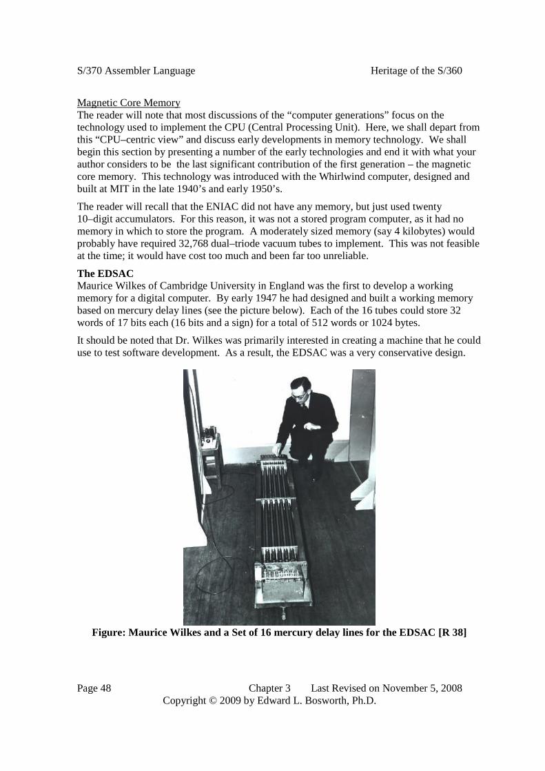
The EDSACMaurice Wilkes of Cambridge University in England was the first to develop a workingmemory for a digital computer. By early 1947 he had designed and built a working memorybased on mercury delay lines (see the picture below). Each of the 16 tubes could store 32words of 17 bits each (16 bits and a sign) for a total of 512 words or 1024 bytes.
It should be noted that Dr. Wilkes was primarily interested in creating a machine that he coulduse to test software development. As a result, the EDSAC was a very conservative design.
Figure: Maurice Wilkes and a Set of 16 mercury delay lines for the EDSAC [R 38]

S/370 Assembler Language Heritage of the S/360
Page 49 Chapter 3 Last Revised on November 5, 2008Copyright © 2009 by Edward L. Bosworth, Ph.D.
The Manchester Mark IThe next step in the development of memory technology was taken at the University ofManchester in England, with the development of the Mark I computer and its predecessor, the“Manchester Baby”. These computers were designed by researchers at the University; themanufacture of the Mark I was contracted out to the Ferranti corporation.
Each of the Manchester Baby and the Manchester/Ferranti Mark I computers used a newtechnology, called the “Williams–Kilburn tube”, as an electrostatic main memory. Thisdevice was developed in 1946 by Frederic C. Williams and Tom Kilburn [R43]. The firstdesign could store either 32 or 64 words (the sources disagree on this) of 32 bits each.
The tube was a cathode ray tube in which the binary bits stored would appear as dots on thescreen. The next figure shows the tube, along with a typical display; this has 32 words of 40bits each. The bright dots store a 1 and the dimmer dots store a 0.
Figure: An Early Williams–Kilburn tube and its displayNote the extra line of 20 bits at the top.
While the Williams–Kilburn tube sufficed for the storage of the prototype Manchester Baby,it was not large enough for the contemplated Mark I. The design team decided to build ahierarchical memory, using double–density Williams–Kilburn tubes (each storing two pagesof thirty–two 40–bit words), backed by a magnetic drum holding 16,384 40–bit words.
The magnetic drum can be seen to hold 512 pages of thirty–two 40–bit words each. The datawere transferred between the drum memory and the electrostatic display tube one page at atime, with the revolution speed of the drum set to match the display refresh speed. The teamused the experience gained with this early block transfer to design and implement the firstvirtual memory system on the Atlas computer in the late 1950’s.
Figure: The IBM 650 Drum Memory

S/370 Assembler Language Heritage of the S/360
Page 50 Chapter 3 Last Revised on November 5, 2008Copyright © 2009 by Edward L. Bosworth, Ph.D.
The MIT Whirlwind and Magnetic Core MemoryThe MIT Whirlwind was designed as a bit-parallel machine with a 5 MHz clock. Thefollowing quote describes the effect of changing the design from one using current technologymemory modules with the new core memory modules.
“Initially it [the Whirlwind] was designed using a rank of sixteen Williams tubes,making for a 16-bit parallel memory. However, the Williams tubes were a limitationin terms of operating speed, reliability, and cost.”
“To solve this problem, Jay W. Forrester and others developed magnetic corememories. When the electrostatic memory was replaced with a primitive corememory, the operating speed of the Whirlwind doubled, and the maintenance timeon the machine fell from four hours per day to two hours per week, and the meantime between memory failures rose from two hours to two weeks! Core memorytechnology was crucial in enabling Whirlwind to perform 50,000 operations persecond in 1952 and to operate reliably for relative long periods of time” [R11]
The reader should consider the previous paragraph carefully and ask how useful computerswould be if we had to spend about half of each working day in maintaining them.
Basically core memory consists of magnetic cores, which are small doughnut-shaped piecesof magnetic material. These can be magnetized in one of two directions: clockwise orcounter-clockwise; one orientation corresponding to a logic 0 and the other to a logic 1.Associated with the cores are current carrying conductors used to read and write the memory.The individual cores were strung by hand on the fine insulated wires to form an array. It is afact that no practical automated core-stringing machine was ever developed; thus corememory was always a bit more costly due to the labor intensity of its construction.
To more clearly illustrate core memory, we include picture from the Sun Microsystems website. Note the cores of magnetic material with the copper wires interlaced.
Figure: Close–Up of a Magnetic Core Memory [R40]
At this point, we leave our discussion of the development of memory technology. While it istrue that memory technology advanced considerably in the years following 1960, we havetaken our narrative far enough to get us to the IBM System/360 family.

S/370 Assembler Language Heritage of the S/360
Page 51 Chapter 3 Last Revised on November 5, 2008Copyright © 2009 by Edward L. Bosworth, Ph.D.
Interlude: Data Storage Technologies In the 1950’s
We have yet to address methods commonly used by early computers for storage of off–linedata; that is data that were not actually in the main memory of the computer. One may validlyask “Why worry about obsolete data storage technologies; we all use disks.” The answer isquite simple, it is the format of these data cards that drove the design of the interactive IBMsystems we use even today. We enter code and data as lines on a terminal using a text editor;we should pretend that we are punching cards.
There were two methods in common use at the time. One of the methods employed punchedpaper tape, with the tape being punched in rows of either five or seven holes. Here are twoviews of typical punched paper tapes from approximately the 1950’s.
Figure: Punched Paper Tape – Fanfold and Rolled
While punched paper tape was commonly used for storage on the smaller computers, such asthe IBM 1620, punched cards were the preferred medium for the larger computers of the early1950’s. Even after the wide availability of magnetic disks and magnetic tape drives, the papercard remained a preferred medium for many data applications until quite late. The mostcommon card was the 80–column punch cards, such as seen in the figure below.
Figure: 80–Column Punch Card (Approximately 75% of Full Size)
These cards would store at most eighty characters, so that the maximum data capacity wasexactly eighty bytes. The card has twelve rows with the bottom ten being numbered 0through 9. There are two additional rows (unmarked in this card) on the top.
S/370 Assembler Language Heritage of the S/360
Page 52 Chapter 3 Last Revised on November 5, 2008Copyright © 2009 by Edward L. Bosworth, Ph.D.
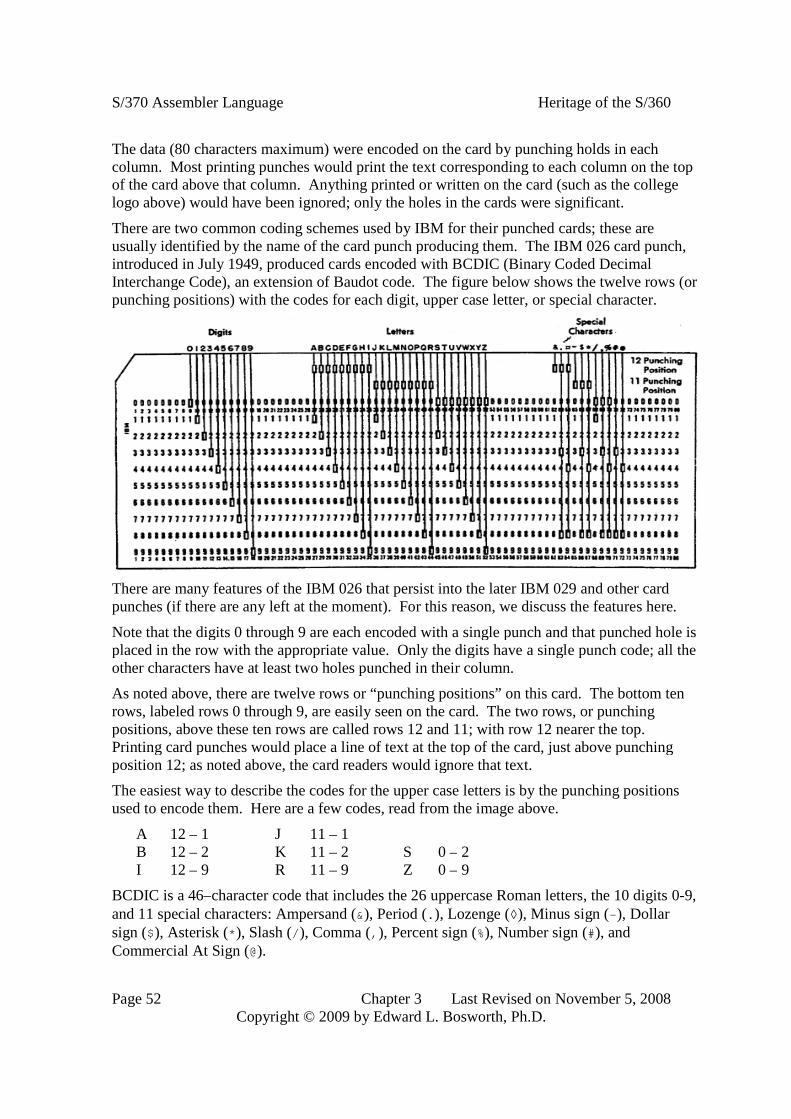
The data (80 characters maximum) were encoded on the card by punching holds in eachcolumn. Most printing punches would print the text corresponding to each column on the topof the card above that column. Anything printed or written on the card (such as the collegelogo above) would have been ignored; only the holes in the cards were significant.
There are two common coding schemes used by IBM for their punched cards; these areusually identified by the name of the card punch producing them. The IBM 026 card punch,introduced in July 1949, produced cards encoded with BCDIC (Binary Coded DecimalInterchange Code), an extension of Baudot code. The figure below shows the twelve rows (orpunching positions) with the codes for each digit, upper case letter, or special character.
There are many features of the IBM 026 that persist into the later IBM 029 and other cardpunches (if there are any left at the moment). For this reason, we discuss the features here.
Note that the digits 0 through 9 are each encoded with a single punch and that punched hole isplaced in the row with the appropriate value. Only the digits have a single punch code; all theother characters have at least two holes punched in their column.
As noted above, there are twelve rows or “punching positions” on this card. The bottom tenrows, labeled rows 0 through 9, are easily seen on the card. The two rows, or punchingpositions, above these ten rows are called rows 12 and 11; with row 12 nearer the top.Printing card punches would place a line of text at the top of the card, just above punchingposition 12; as noted above, the card readers would ignore that text.
The easiest way to describe the codes for the upper case letters is by the punching positionsused to encode them. Here are a few codes, read from the image above.
A 12 – 1 J 11 – 1B 12 – 2 K 11 – 2 S 0 – 2I 12 – 9 R 11 – 9 Z 0 – 9
BCDIC is a 46–character code that includes the 26 uppercase Roman letters, the 10 digits 0-9,and 11 special characters: Ampersand (&), Period (.), Lozenge (◊), Minus sign (-), Dollarsign ($), Asterisk (*), Slash (/), Comma (,), Percent sign (%), Number sign (#), andCommercial At Sign (@).
S/370 Assembler Language Heritage of the S/360
Page 53 Chapter 3 Last Revised on November 5, 2008Copyright © 2009 by Edward L. Bosworth, Ph.D.
The reader will note that this code omits all lower case letters and a great number of usefulcharacters. The obvious conclusion is that it predates any high–level programming language,as it lacks coding for the plus sign,”+”, as well as parentheses.
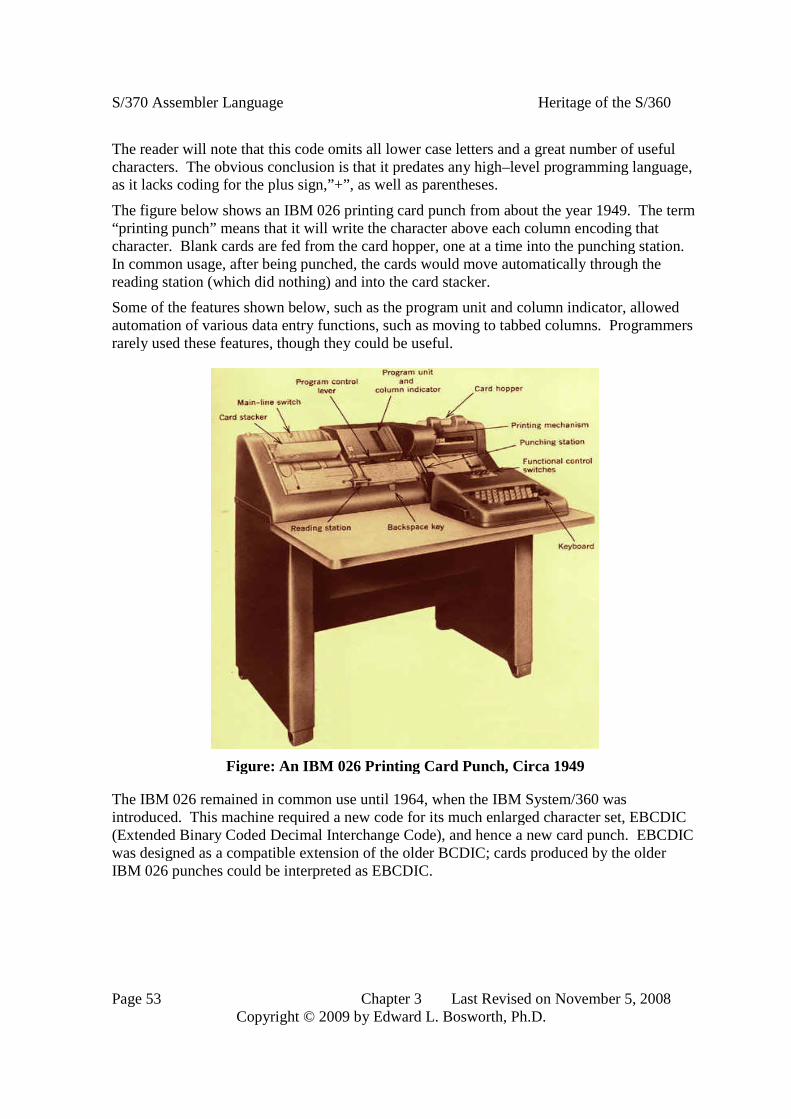
The figure below shows an IBM 026 printing card punch from about the year 1949. The term“printing punch” means that it will write the character above each column encoding thatcharacter. Blank cards are fed from the card hopper, one at a time into the punching station.In common usage, after being punched, the cards would move automatically through thereading station (which did nothing) and into the card stacker.
Some of the features shown below, such as the program unit and column indicator, allowedautomation of various data entry functions, such as moving to tabbed columns. Programmersrarely used these features, though they could be useful.
Figure: An IBM 026 Printing Card Punch, Circa 1949
The IBM 026 remained in common use until 1964, when the IBM System/360 wasintroduced. This machine required a new code for its much enlarged character set, EBCDIC(Extended Binary Coded Decimal Interchange Code), and hence a new card punch. EBCDICwas designed as a compatible extension of the older BCDIC; cards produced by the olderIBM 026 punches could be interpreted as EBCDIC.

S/370 Assembler Language Heritage of the S/360
Page 54 Chapter 3 Last Revised on November 5, 2008Copyright © 2009 by Edward L. Bosworth, Ph.D.
The IBM 029 Printing Card Punch was used to encode characters in EDCDIC on a standardeighty–column punch card. The format of the card was retained while the code changed.Here is an illustration of the punch code produced by the IBM 029; the card displays each ofthe 64 characters available for this format. Note again that lower case letters are missing.
Note that the encodings for the ten digits and twenty–six upper case letters are retained fromthe BCDIC codes of the IBM 026. This example shows the print representation of eachcharacter above the column that encodes it. The IBM 026 also had the ability to print in thisarea; it is just that the example we noted did not have that printing. Comparison of the pictureof the IBM 029 (below) and the IBM 026 (above) show only cosmetic change.
Figure: The IBM 029 Printing Card Punch (1964)
S/370 Assembler Language Heritage of the S/360
Page 55 Chapter 3 Last Revised on November 5, 2008Copyright © 2009 by Edward L. Bosworth, Ph.D.
It is worth noting that IBM seriously considered adoption of ASCII as its method for internalstorage of character data for the System/360. The American Standard Code for InformationInterchange was approved in 1963 and supported by IBM. However the ASCII code set wasnot compatible with the BCDIC used on a very large installed base of support equipment,such as the IBM 026. Transition to an incompatible character set would have required anyadopter of the new IBM System/360 to also purchase or lease an entirely new set of peripheralequipment; this would have been a deterrence to early adoption.
It is a little known fact that the CPU (Central Processing Unit) on an early System/360implementation included an “ASCII bit” in the PSW (Program Status Word). When set, theS/360 would process characters encoded in ASCII; when cleared the EBCDIC code was used.
It is an interesting study to remark on the design of the EBCDIC scheme and how it wasrelated to the punch card codes used by the IBM 029 card punch. One should be very carefuland precise at this moment; the punch card codes were not EBCDIC.
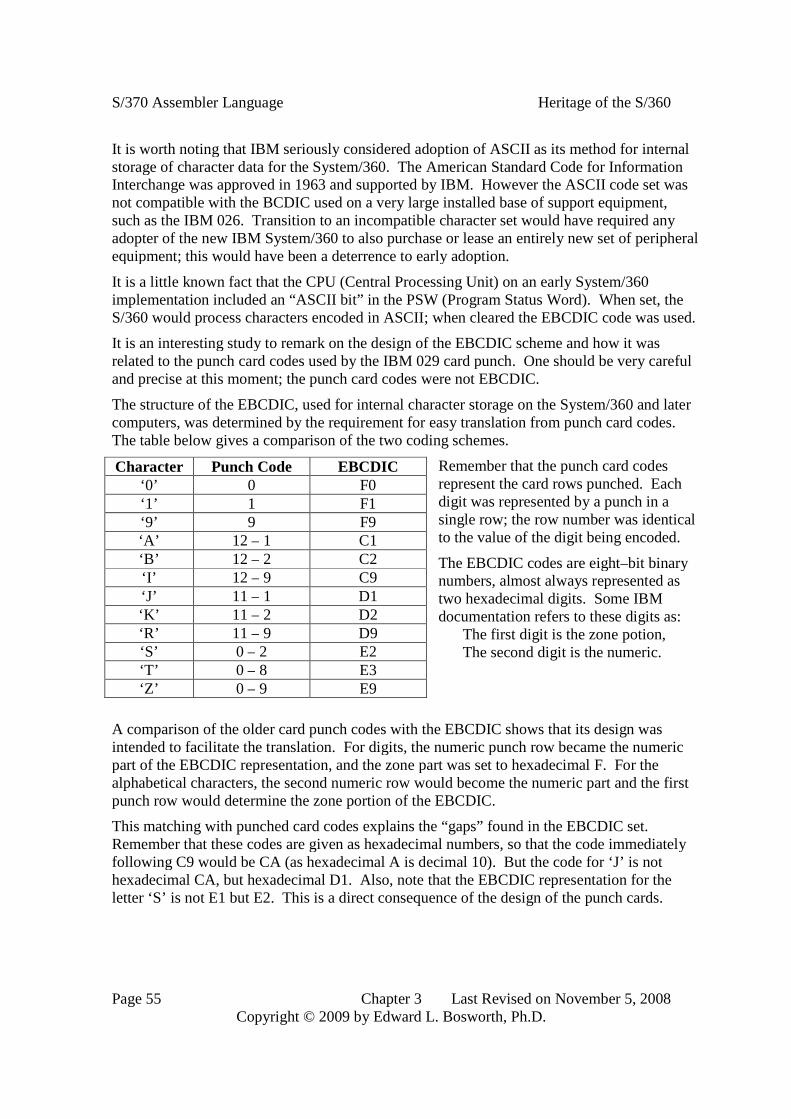
The structure of the EBCDIC, used for internal character storage on the System/360 and latercomputers, was determined by the requirement for easy translation from punch card codes.The table below gives a comparison of the two coding schemes.
Remember that the punch card codesrepresent the card rows punched. Eachdigit was represented by a punch in asingle row; the row number was identicalto the value of the digit being encoded.
The EBCDIC codes are eight–bit binarynumbers, almost always represented astwo hexadecimal digits. Some IBMdocumentation refers to these digits as:
The first digit is the zone potion,The second digit is the numeric.
A comparison of the older card punch codes with the EBCDIC shows that its design wasintended to facilitate the translation. For digits, the numeric punch row became the numericpart of the EBCDIC representation, and the zone part was set to hexadecimal F. For thealphabetical characters, the second numeric row would become the numeric part and the firstpunch row would determine the zone portion of the EBCDIC.
This matching with punched card codes explains the “gaps” found in the EBCDIC set.Remember that these codes are given as hexadecimal numbers, so that the code immediatelyfollowing C9 would be CA (as hexadecimal A is decimal 10). But the code for ‘J’ is nothexadecimal CA, but hexadecimal D1. Also, note that the EBCDIC representation for theletter ‘S’ is not E1 but E2. This is a direct consequence of the design of the punch cards.
Character Punch Code EBCDIC‘0’ 0 F0‘1’ 1 F1‘9’ 9 F9‘A’ 12 – 1 C1‘B’ 12 – 2 C2‘I’ 12 – 9 C9‘J’ 11 – 1 D1‘K’ 11 – 2 D2‘R’ 11 – 9 D9‘S’ 0 – 2 E2‘T’ 0 – 8 E3‘Z’ 0 – 9 E9

S/370 Assembler Language Heritage of the S/360
Page 56 Chapter 3 Last Revised on November 5, 2008Copyright © 2009 by Edward L. Bosworth, Ph.D.
Line Printers: The Output Machines
There were two common methods for output of data from early IBM machines: the cardpunch and the line printer. The card punch was just a computer controlled version of themanual card punches, though with distinctively different configurations. All card punches,manual or automatic, produced cards to be read by the computer’s card reader.
The standard printer of the time was a line printer, meaning that it printed output one line at atime. These devices were just extremely fast and sophisticated typewriters, using an inkedribbon to provide the ink for the printed characters. The ink–jet printer and the laser printereach is a device of a later decade. One should note that only the “high end” laser printers, ofthe type found in print shops today, are capable of matching the output of a line printer.
The standard printer formats called for output of data into fixed width columns; the maximumwidth being either 80 columns per line or 132 columns per line. The first picture shows anIBM 716 printer from about 1952. The second show an IBM 1403 printer introduced in 1959.Each appears to be using 132–column width paper.
Figure: The IBM 716 Printer
Figure: The IBM 1403 Printer

S/370 Assembler Language Heritage of the S/360
Page 57 Chapter 3 Last Revised on November 5, 2008Copyright © 2009 by Edward L. Bosworth, Ph.D.
IBM: Generation 0
We now examine the state of affairs for IBM at the end of the 1940’s. This for IBM was theend of “Generation 0”; that is the time during which electromechanical calculators werephased out and vacuum tube computers were introduced.
The author of this textbook wishes to state that the source for almost all of the material in thissection is the IBM history web site (http://www-03.ibm.com/ibm/history/exhibits/).
IBM was incorporated in the state of New York on June 16, 1911 as the C –T–R Company(Computing–Tabulating–Recording Company), and renamed as the International BusinessMachines Corporation on February 14, 1924. Many of its more important products have rootsin the companies of the late 19th century that were merged to form the C–T–R Company.
One can argue that the lineage of most of IBM’s product line in the late 1940’s can be tracedback to the work of Dr. Herman Hollerith, who first demonstrated his tabulating systems in1889. This system used punched cards to record the data, and a electromechanical calculatorto extract information from the cards.
Herman Hollerith's Tabulating System, shown in the figureto the left, was used in the U.S. Census of 1890. It reduceda nearly 10–year long process to two and a half years andsaved $5 million. The Hollerith, Punch Card TabulatingMachine used an electric current to sense holes in punchedcards and keep a running total of data. Capitalizing on hissuccess, Hollerith formed the Tabulating MachineCompany in 1896. This was one of the companies that wasmerged into the C–T–R Company in 1911.
We mention the Hollerith Tabulator of 1890 for two reasons. The first is that it represented asignificant innovation for the time, one that the descendant company, IBM, could be proud of.The second reason is that it illustrates the design of many of the IBM products of the first halfof the twentieth century: accept cards as input, process the data on the cards, and produceinformation for use by the managers of the businesses using those calculators.
As noted indirectly above, IBM’s predecessor company, the C–T–R Company, was formed in1911 by the merger of three companies: Hollerith’s Tabulating Machine Company, theComputing Scale Company of America, and the International Time Recording Company. In1914, Thomas J. Watson, Sr. was persuaded to join the company as general manager. Mr.Watson was a formidable figure, playing a large role atIBM until the early 1950’s.
We now jump ahead to 1933, at which time IBMintroduced the Type 285 Numeric Printing Tabulator. Thegoal of this device, as well as its predecessors in the1920’s, was to reduce the error caused by the hand copyingof numbers from the mechanical counters used in previoustabulators. By this time, the data cards had been expandedto 80 columns. These cards were fed from a tray at theright of the machine, and passed over the tabulating units.

S/370 Assembler Language Heritage of the S/360
Page 58 Chapter 3 Last Revised on November 5, 2008Copyright © 2009 by Edward L. Bosworth, Ph.D.
Early tabulating machines were essentially single–function calculators. Starting in 1906,tabulators were made more flexible by addition of a wiring panel to let users control theiractions to some degree, thus allowing the same machine to be sold into different markets(government, railroad, etc) and used for different purposes. But this also meant that if onemachine were to be used for different jobs, it would have to be rewired between each job,often a lengthy process that kept the machine offline for extended periods. In 1928, IBMbegan to manufacture machines with removable wiring panels, or "plugboards", so programscould be prewired and swapped in and out instantly to change jobs.
One example of this is the IBM 402 Accounting Machine, introduced in 1948. It was one ofthe “400 series”, each of which could read standard 80 column cards, accumulate sums,subtotals, and balances, and print reports, all under the control of instructions wired into itscontrol panel. In the figure below, the Type 402 (on the left) is shown attached to a Type 519Summary Punch (on the right), allowing totals accumulated by the accounting machine to bepunched to cards for later use.
Figure: IBM 402 Attached to an IBM 519
The 402 series, like the 405 before it, used a typebar print mechanism, in which each column(up to 88, depending on model and options) has its own type bar. Long type bars (on the leftin the photo below) contain letters and digits; short ones contain only digits (each kind of typebar also includes one or two symbols such as ampersand or asterisk). Type bars shoot up anddown independently, positioning the desired character for impact printing.
Figure: IBM 402 Tabular Typebar

S/370 Assembler Language Heritage of the S/360
Page 59 Chapter 3 Last Revised on November 5, 2008Copyright © 2009 by Edward L. Bosworth, Ph.D.
Here are two views of a plugboard, as used on the IBM Type 402 Accounting Machine.
Figure: The Plugboard Receptacle
Figure: A Wired Plugboard

S/370 Assembler Language Heritage of the S/360
Page 60 Chapter 3 Last Revised on November 5, 2008Copyright © 2009 by Edward L. Bosworth, Ph.D.
As suggested by the above discussions, most financial computing in the 1930’s and 1940’srevolved around the use of punched cards to store data. The figure below shows a “cardshop” from 1950. These 11 men and women are operating an IBM electric accountingmachine installation. Seen here (at left) is an IBM 523 gang summary punch, which couldprocess 100 cards a minute and (in the middle) an IBM 82 high-speed sorter, which couldprocess 650 punched cards a minute. This may be seen as an essential part of an IBM shop inthe late 1940’s: process financial data and produce results for managers.
Figure: People with Card Equipment
We close this section of our discussion with a picture of the largest electromechanicalcalculator ever built, the Harvard Mark I, also known as the IBM Automatic SequenceControlled Calculator. It was 51 feet long, 8 feet high, and weighed five tons. It was the firstfully automatic computer to be completed; once it started it needed no human intervention. Itis best seen as an ancestor of the ENIAC and early IBM digital computers.
Figure: The Harvard Mark–I (1944)

S/370 Assembler Language Heritage of the S/360
Page 61 Chapter 3 Last Revised on November 5, 2008Copyright © 2009 by Edward L. Bosworth, Ph.D.
The Evolution of the IBM–360We now return to a discussion of “Big Iron”, a name given informally to the larger IBMmainframe computers of the time. Much of this discussion is taken from an article in the IBMJournal of Research and Development [R46], supplemented by articles from [R1]. We tracethe evolution of IBM computers from the first scientific computer ( the IBM 701, announcedin May 1952) through the early stages of the S/360 (announced in March 1964).
We begin this discussion by considering the situation as of January 1, 1954. At the time, IBMhas three models announced and shipping. Two of these were the IBM 701 for scientificcomputations and the IBM 702 for financial calculations (announced in September 1953),.Each of the designs used Williams–Kilburn tubes for primary memory, and each wasimplemented using vacuum tubes in the CPU. Neither computer supported both floating–point (scientific) and packed decimal (financial) arithmetic, as the cost to support both wouldhave been excessive. As a result, there were two “lines”: scientific and commercial.
The third model was the IBM 650. It was designed as “a much smaller computer that wouldbe suitable for volume production. From the outset, the emphasis was on reliability andmoderate cost”. The IBM 650 was a serial, decimal, stored–program computer with fixedlength words each holding ten decimal digits and a sign. Later models could be equippedwith the IBM 305 RAMAC (the disk memory discussed and pictured above). When equippedwith terminals, the IBM 650 started the shift towards transaction–oriented processing.
The figure below can be considered as giving the “family tree” of the IBM System/360.Note that there are four “lines”: the IBM 650 line, the IBM 701 line, IBM 702 line, and theIBM 7030 (Stretch). The System/360 (so named because it handled “all 360 degrees ofcomputing”) was an attempt to consolidate these lines and reduce the multiplicity of distinctsystems, each with its distinct maintenance problems and costs.
Figure: The IBM System/360 “Family Tree”

S/370 Assembler Language Heritage of the S/360
Page 62 Chapter 3 Last Revised on November 5, 2008Copyright © 2009 by Edward L. Bosworth, Ph.D.
As mentioned above, in the 1950’s IBM supported two product lines: scientific computers(beginning with the IBM 701) and commercial computes (beginning with the IBM 702).Each of these lines was redesigned and considerably improved in 1954.
Generation 1 of the Scientific LineIn the IBM 704 (announced in May 1954), the Williams–Kilburn tube memory was replacedby magnetic–core memory with up to 32768 36–bit words. This eliminated the most difficultmaintenance problem and allowed users to run larger programs. At the time, theorists hadestimated that a large computer would require only a few thousand words of memory. Evenat this time, the practical programmers wanted more than could be provided.
The IBM 704 also introduced hardware support for floating–point arithmetic, which wasomitted from the IBM 701 in an attempt to keep the design “simple and spartan” [R46]. Italso added three index registers, which could be used for loops and address modification. Asmany scientific programs make heavy use of loops over arrays, this was a welcome addition.
The IBM 709 (announced in January 1957) was basically an upgraded IBM 704. The mostimportant new function was then called a “data–synchronizer unit”; it is now called an “I/OChannel”. Each channel was an individual I/O processor that could address and access mainmemory to store and retrieve data independently of the CPU. The CPU would interact withthe I/O Channels by use of special instructions that later were called channel commands.
It was this flexibility, as much as any other factor, that lead to the development of a simplesupervisory program called the IOCS (I/O Control System). This attempt to provide supportfor the task of managing I/O channels and synchronizing their operation with the CPUrepresents an early step in the evolution of the operating system.
Generation 1 of the Commercial LineThe IBM 702 series differed from the IBM 701 series in many ways, the most important ofwhich was the provision for variable–length digital arithmetic. In contrast to the 36–bit wordorientation of the IBM 701 series, this series was oriented towards alphanumeric arithmetic,with each character being encoded as 6 bits with an appended parity check bit. Numberscould have any length from 1 to 511 digits, and were terminated by a “data mark”.
The IBM 705 (announced in October 1954) represented a considerable upgrade to the 702.The most significant change was the provision of magnetic–core memory, removing aconsiderable nuisance for the maintenance engineers. The size of the memory was at firstdoubled and then doubled again to 40,000 characters. Later models could be provided withone or more “data–synchronizer units”, allowing buffered I/O independent of the CPU.
Generation 2 of the Product LinesAs noted above, the big change associated with the transition to the second generation is theuse of transistors in the place of vacuum tubes. Compared to an equivalent vacuum tube, atransistor offers a number of significant advantages: decreased power usage, decreased cost,smaller size, and significantly increased reliability. These advantages facilitated the design ofincreasingly complex circuits of the type required by the then new second generation.
The IBM 7070 (announced in September 1958 as an upgrade to the IBM 650) was the firsttransistor based computer marketed by IBM. This introduced the use of interrupt–driven I/Oas well as the SPOOL (Simultaneous Peripheral Operation On Line) process for managingshared Input/Output devices.

S/370 Assembler Language Heritage of the S/360
Page 63 Chapter 3 Last Revised on November 5, 2008Copyright © 2009 by Edward L. Bosworth, Ph.D.
The IBM 7090 (announced in December 1958) was a transistorized version of the IBM 709with some additional facilities. The IBM 7080 (announced in January 1960) likewise was atransistorized version of the IBM 705. Each model was less costly to maintain and morereliable than its tube–based predecessor, to the extent that it was judged to be a “qualitativelydifferent kind of machine” [R46].
The IBM 7090 (and later IBM 7094) were modified by researchers at M.I.T. in order to makepossible the CTSS (Compatible Time–Sharing System), the first major time–sharing system.Memory was augmented by a second 32768–word memory bank. User programs occupiedone bank while the operating system resided in the other. User memory was divided into 128memory–protected blocks of 256 words, and access was limited by boundary registers.
The IBM 7094 was announced on January 15, 1962. The CTSS effort was begun in 1961,with a version being demonstrated on an IBM 709 in November 1961. CTSS was formallypresented in a paper at the Joint Computer Conference in May, 1962. Its design affected lateroperating systems, including MULTICS and its derivatives, UNIX and MS–DOS.
As a last comment here, the true IBM geek will note the omission of any discussion of theIBM 1401 line. These machines were often used in conjunction with the 7090 or 7094,handling the printing, punching, and card reading chores for the latter. It is just not possibleto cover every significant machine.
The IBM 7030 (Stretch)In late 1954, IBM decided to undertake a very ambitious research project, with the goal ofbenefiting from the experience gained in the previous three project lines. In 1955, it wasdecided that the new machine should be at least 100 times as fast as either the IBM 704 or theIBM 705; hence the informal name “Stretch” as it “stretched the technology”.
In order to achieve these goals, the design of the IBM 7030 required a considerable number ofinnovations in technology and computer organization; a few are listed here.
1. A new type of germanium transistor, called “drift transistor” was developed. Thesefaster transistors allowed the circuitry in the Stretch to run ten times faster.
2. A new type of core memory was developed; it was 6 times faster than the older core.
3. Memory was organized into multiple 128K–byte units accessed by low–orderinterleaving, so that successive words were stored in different banks. As a result,new data could be retrieved at a rate of one word every 200 nanoseconds, eventhough the memory cycle time was 2.1 microseconds (2,100 nanoseconds).
4. Instruction lookahead (now called “pipelining”) was introduced. At any point intime, six instructions were in some phase of execution in the CPU.
5. New disk drives, with multiple read/write arms, were developed. The capacity andtransfer rate of these devices lead to the abandonment of magnetic drums.
6. A pair of boundary registers were added so as to provide the storage protectionrequired in a multiprogramming environment.

S/370 Assembler Language Heritage of the S/360
Page 64 Chapter 3 Last Revised on November 5, 2008Copyright © 2009 by Edward L. Bosworth, Ph.D.
It is generally admitted that the Stretch did not meet its design goal of a 100 times increase inthe performance of the earlier IBM models. Here is the judgment by IBM from 1981 [R46].
“For a typical 704 program, Stretch fell short of is performance target of one hundred timesthe 704, perhaps by a factor of two. In applications requiring the larger storage capacity andword length of Stretch, the performance factor probably exceeded one hundred, butcomparisons are difficult because such problems were not often tackled on the 704.” [R46]
It seems that production of the IBM 7030 (Stretch) was limited to nine machines, one for LosAlamos National Labs, one (called “Harvest”) for the National Security Agency, and 7 more.
Smaller Integrated Circuits (Generation 3 – from 1966 to 1972)In one sense, the evolution of computer components can be said to have stopped in 1958 withthe introduction of the transistor; all future developments merely represent the refinement ofthe transistor design. This statement stretches the truth so far that it hardly even makes thisauthor’s point, which is that packaging technology is extremely important.
What we see in the generations following the introduction of the transistor is an aggressiveminiaturization of both the transistors and the traces (wires) used to connect the circuitelements. This allowed the creation of circuit modules with component densities that couldhardly have been imagined a decade earlier. Such circuit modules used less power and weremuch faster than those of the second generation; in electronics smaller is faster. They alsolent themselves to automated manufacture, thus increasing component reliability.
The Control Unit and EmulationIn order to better explain one of the distinctive features of the IBM System/360 family, it isnecessary to take a detour and discuss the function of the control unit in a stored programcomputer. Basically, the control unit tells the computer what to do.
All modern stored program computers execute programs that are a sequence of binarymachine–language instructions. This sequence of instructions corresponds either to anassembly language program or a program in a higher–level language, such as C++ or Java.
The basic operation of a stored program computer is called “fetch–execute”, with manyvariants on this name. Each instruction to be executed is fetched from memory and depositedin the Instruction Register, which is a part of the control unit. The control unit interprets thismachine instruction and issues the signals that cause the computer to execute it.
Figure: Schematic of the Control Unit

S/370 Assembler Language Heritage of the S/360
Page 65 Chapter 3 Last Revised on November 5, 2008Copyright © 2009 by Edward L. Bosworth, Ph.D.
There are two ways in which a control unit may be organized. The most efficient way is tobuild the unit entirely from basic logic gates. For a moderately–sized instruction set with thestandard features expected, this leads to a very complex circuit that is difficult to test.
In 1951, Maurice V. Wilkes (designer of the EDSAC, see above) suggested an organizationfor the control unit that was simpler, more flexible, and much easier to test and validate. Thiswas called a “microprogrammed control unit”. The basic idea was that control signals canbe generated by reading words from a micromemory and placing each in an output buffer.
In this design, the control unit interprets the machine language instruction and branches to asection of the micromemory that contains the microcode needed to emit the proper controlsignals. The entire contents of the micromemory, representing the sequence of control signalsfor all of the machine language instructions is called the microprogram. All we need toknow is that the microprogram is stored in a ROM (Read Only Memory) unit.
While microprogramming was sporadically investigated in the 1950’s, it was not until about1960 that memory technology had matured sufficiently to allow commercial fabrication of amicromemory with sufficient speed and reliability to be competitive. When IBM selected thetechnology for the control units of some of the System/360 line, its primary goal was thecreation of a unit that was easily tested. Then they got a bonus; they realized that adding theappropriate blocks of microcode could make a S/360 computer execute machine code foreither the IBM 1401 or IBM 7094 with no modification. This greatly facilitated upgradingfrom those machines and significantly contributed to the popularity of the S/360 family.
The IBM System/360As noted above, the IBM chose to replace a number of very successful, but incompatible,computer lines with a single computer family, the System/360. The goal, according to anIBM history web site [R48] was to “provide an expandable system that would serve everydata processing need”. The initial announcement on April 7, 1964 included Models 30, 40,50, 60, 62, and 70 [R49]. The first three began shipping in mid–1965, and the last three werereplaced by the Model 65 (shipped in November 1965) and Model 75 (January 1966).
The introduction of the System/360 is also the introduction of the term “architecture”as applied to computers. The following quotes are taken from one of the first papersdescribing the System/360 architecture [R46].
“The term architecture is used here to describe the attributes of a system as seen bythe programmer,, i.e., the conceptual structure and functional behavior, as distinctfrom the organization of the data flow and controls, the logical design,and the physical implementation.”
“In the last few years, many computer architects have realized, usually implicitly,that logical structure (as seen by the programmer) and physical structure (as seenby the engineer) are quite different. Thus, each may see registers, counters, etc.,that to the other are not at all real entities. This was not so in the computers of the1950’s. The explicit recognition of the duality of the structure opened the wayfor the compatibility within System/360.”
S/370 Assembler Language Heritage of the S/360
Page 66 Chapter 3 Last Revised on November 5, 2008Copyright © 2009 by Edward L. Bosworth, Ph.D.
To see the difference, consider the sixteen general–purpose registers (R0 – R15) in theSystem/360 architecture. All models implement these registers and use them in exactly thesame way; this is a requirement of the architecture. As a matter of implementation, a fewof the lower end S/360 family actually used dedicated core memory for the registers, whilethe higher end models used solid state circuitry on the CPU board.
The difference between organization and implementation is seen by considering the twocomputer pairs: the 709 and 7090, and the 705 and 7080. The IBM 7090 had the sameorganization (hence the same architecture) as the IBM 709; the implementation was different.The IBM 709 used vacuum tubes; the IBM 7090 replaced these with transistors.
The requirement for the System/360 design is that all models in that series would be“strictly program compatible, upward and downward, at the program bit level”. [R46]
“Here it [strictly program compatible] means that a valid program, whose logic willnot depend implicitly upon time of execution and which runs upon configuration A,will also run on configuration B if the latter includes as least the required storage, atleast the required I/O devices, and at least the required optional features.”
“Compatibility would ensure that the user’s expanding needs be easily accommodatedby any model. Compatibility would also ensure maximum utility of programmingsupport prepared by the manufacturer, maximum sharing of programs generated by theuser, ability to use small systems to back up large ones, and exceptional freedom inconfiguring systems for particular applications.”
Additional design goals for the System/360 include the following.
1. The System/360 was intended to replace two mutually incompatible productlines in existence at the time.
a) The scientific series (701, 704, 7090, and 7094) that supported floatingpoint arithmetic, but not decimal arithmetic.
b) The commercial series (702, 705, and 7080) that supported decimalarithmetic, but not floating point arithmetic.
2. The System/360 should have a “compatibility mode” that would allow itto run unmodified machine code from the IBM 1401 – at the time a verypopular business machine with a large installed base.
This was possible due to the use of a microprogrammed control unit. If youwant to run native S/360 code, access that part of the microprogram. If youwant to run IBM 1401 code, just switch to the microprogram for that machine.
3. The Input/Output Control Program should be designed to allow execution bythe CPU itself (on smaller machines) or execution by separate I/O Channelson the larger machines.
4. The system must allow for autonomous operation with very little intervention bya human operator. Ideally this would be limited to mounting and dismountingmagnetic tapes, feeding punch cards into the reader, and delivering output.
5. The system must support some sort of extended precision floating pointarithmetic, with more precision than the 36–bit system then in use.

S/370 Assembler Language Heritage of the S/360
Page 67 Chapter 3 Last Revised on November 5, 2008Copyright © 2009 by Edward L. Bosworth, Ph.D.
The design goal for the series is illustrated by the following scenario. It should be noted thatthis goal of upward compatibility has persisted to the present day, in which there seem to be atleast fifty models of the z/10, all compatible with each other and differing only inperformance (number of transactions per second) and cost. Here is the scenario.
1. You have a small company. It needs only a small computer to handle itscomputing needs. You lease an IBM System 360/30. You use it in emulationmode to run your IBM 1401 programs unmodified.
2. Your company grows. You need a bigger computer. Lease a 360/50.
3. You hit the “big time”. Turn in the 360/50 and lease a 360/91.You never need to rewrite or recompile your existing programs.You can still run your IBM 1401 programs without modification.
The System/360 Evolves into the System 370In June 1970, IBM announced the S/370 as a successor to the System/360. This introducedanother design feature of the evolving series; each model would be backwardly compatiblewith the previous models in that it would run code assembled on the earlier models. Thus, theS/370 would run S/360 code unaltered, and later models would run both S/360 and S/370code unaltered. It is this fact that we rely on when we are running S/370 assembler code on amodern z/10 Enterprise Server, which was introduced in 2008.
The S/370 underwent a major upgrade to the S/370–XA (S/370 extended architecture) in early1983. At this time the address space was extended from 24 bits to 31 bits, allowing the CPUto address two gigabytes of memory (1 GB = 230 bytes) rather than just 16 MB (224 bytes).
While the IBM mainframe architecture has evolved further since the introduction of theS/370, it is here that we stop our overview. The primary reason for this is that this course hasbeen designed to teach System/370 Assembler Language, focusing on the basics of thatlanguage and avoiding the extensions of the language introduced with the later models.
The Mainframe Evolves: The z10 Enterprise Servers.While this textbook and the course based on it will focus on the state of mainframe assemblerwriting as of about 1979 (the date at which the textbook we previously used was published), itis important to know where IBM has elected to take this architecture. The present state of thedesign is reflected in the z/Series, first introduced in the year 2000.
The major design goal of the z/Series is reflected in its name, in which the “z” stands for“Zero Down–Time”. The mainframe has evolved into a highly reliable transaction server forvery high transaction volumes. A typical transaction takes place every time a credit card isused for a purchase. The credit card reader at the merchant location contacts a central server,which might be a z10, and the transaction is recorded for billing later. In such a high–volumebusiness, loss of the central server for as much as an hour could result in the loss of millionsof dollars in profits to a company. It is this model for which IBM designed the mainframe.
We end this chapter by noting that some at IBM prefer to discontinue the use of the term“mainframe”, considering it to be obsolete. In this thought, the term would refer to an earlyS/360 or S/370, and not to the modern z/Series systems which are both more powerful andmuch smaller in physical size. The preferred term would be “Enterprise Server”. The onlydifficulty is that the customers prefer the term “mainframe”, so it stays.