Chapter 3: Crystal Structure - Penn State Mechanical ... · The crystal structure can exert a...
25
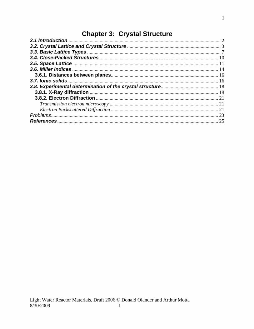
1 Chapter 3: Crystal Structure 3.1 Introduction........................................................................................................................... 2 3.2. Crystal Lattice and Crystal Structure ........................................................................... 3 3.3. Basic Lattice Types ........................................................................................................... 7 3.4. Close-Packed Structures ............................................................................................... 10 3.5. Space Lattice ..................................................................................................................... 11 3.6. Miller indices ..................................................................................................................... 14 3.6.1. Distances between planes...................................................................................... 16 3.7. Ionic solids ......................................................................................................................... 16 3.8. Experimental determination of the crystal structure.............................................. 18 3.8.1. X-Ray diffraction ....................................................................................................... 19 3.8.2. Electron Diffraction .................................................................................................. 21 Transmission electron microscopy ....................................................................................... 21 Electron Backscattered Diffraction ...................................................................................... 21 Problems...................................................................................................................................... 23 References ................................................................................................................................. 25 Light Water Reactor Materials, Draft 2006 © Donald Olander and Arthur Motta 8/30/2009 1
Transcript of Chapter 3: Crystal Structure - Penn State Mechanical ... · The crystal structure can exert a...
1
Chapter 3: Crystal Structure 3.1 Introduction........................................................................................................................... 2 3.2. Crystal Lattice and Crystal Structure ........................................................................... 3 3.3. Basic Lattice Types ........................................................................................................... 7 3.4. Close-Packed Structures ............................................................................................... 10 3.5. Space Lattice ..................................................................................................................... 11 3.6. Miller indices ..................................................................................................................... 14
3.6.1. Distances between planes...................................................................................... 16 3.7. Ionic solids......................................................................................................................... 16 3.8. Experimental determination of the crystal structure.............................................. 18
3.8.1. X-Ray diffraction ....................................................................................................... 19 3.8.2. Electron Diffraction .................................................................................................. 21
Transmission electron microscopy ....................................................................................... 21 Electron Backscattered Diffraction ...................................................................................... 21
Problems...................................................................................................................................... 23 References ................................................................................................................................. 25
Light Water Reactor Materials, Draft 2006 © Donald Olander and Arthur Motta 8/30/2009 1
2
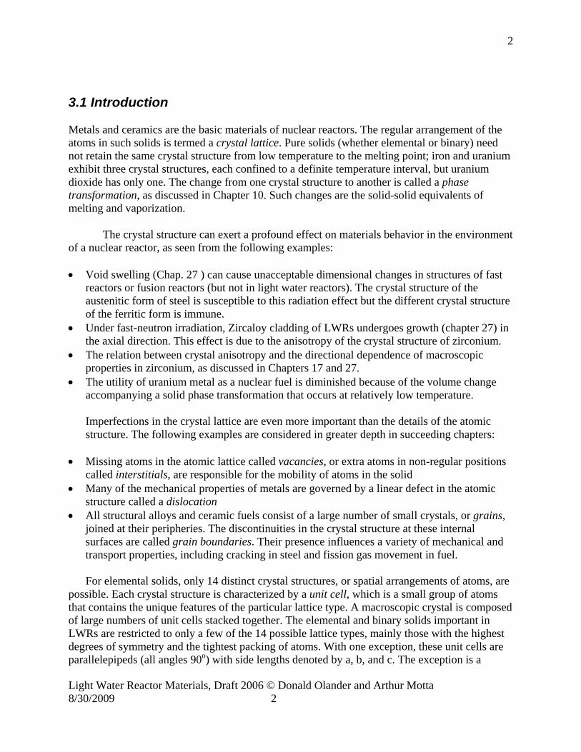
3.1 Introduction Metals and ceramics are the basic materials of nuclear reactors. The regular arrangement of the atoms in such solids is termed a crystal lattice. Pure solids (whether elemental or binary) need not retain the same crystal structure from low temperature to the melting point; iron and uranium exhibit three crystal structures, each confined to a definite temperature interval, but uranium dioxide has only one. The change from one crystal structure to another is called a phase transformation, as discussed in Chapter 10. Such changes are the solid-solid equivalents of melting and vaporization. The crystal structure can exert a profound effect on materials behavior in the environment of a nuclear reactor, as seen from the following examples: • Void swelling (Chap. 27 ) can cause unacceptable dimensional changes in structures of fast
reactors or fusion reactors (but not in light water reactors). The crystal structure of the austenitic form of steel is susceptible to this radiation effect but the different crystal structure of the ferritic form is immune.
• Under fast-neutron irradiation, Zircaloy cladding of LWRs undergoes growth (chapter 27) in the axial direction. This effect is due to the anisotropy of the crystal structure of zirconium.
• The relation between crystal anisotropy and the directional dependence of macroscopic properties in zirconium, as discussed in Chapters 17 and 27.
• The utility of uranium metal as a nuclear fuel is diminished because of the volume change accompanying a solid phase transformation that occurs at relatively low temperature.
Imperfections in the crystal lattice are even more important than the details of the atomic structure. The following examples are considered in greater depth in succeeding chapters:
• Missing atoms in the atomic lattice called vacancies, or extra atoms in non-regular positions called interstitials, are responsible for the mobility of atoms in the solid
• Many of the mechanical properties of metals are governed by a linear defect in the atomic structure called a dislocation
• All structural alloys and ceramic fuels consist of a large number of small crystals, or grains, joined at their peripheries. The discontinuities in the crystal structure at these internal surfaces are called grain boundaries. Their presence influences a variety of mechanical and transport properties, including cracking in steel and fission gas movement in fuel.
For elemental solids, only 14 distinct crystal structures, or spatial arrangements of atoms, are
possible. Each crystal structure is characterized by a unit cell, which is a small group of atoms that contains the unique features of the particular lattice type. A macroscopic crystal is composed of large numbers of unit cells stacked together. The elemental and binary solids important in LWRs are restricted to only a few of the 14 possible lattice types, mainly those with the highest degrees of symmetry and the tightest packing of atoms. With one exception, these unit cells are parallelepipeds (all angles 90o) with side lengths denoted by a, b, and c. The exception is a
Light Water Reactor Materials, Draft 2006 © Donald Olander and Arthur Motta 8/30/2009 2
3
structure whose unit cell is a hexagonal prism with only two characteristic dimensions. Only the parallelepiped with all sides of equal length (i.e., a cube) is isotropic. All the others are anisotropic, meaning that properties differ in the principal coordinate directions.
3.2. Crystal Lattice and Crystal Structure
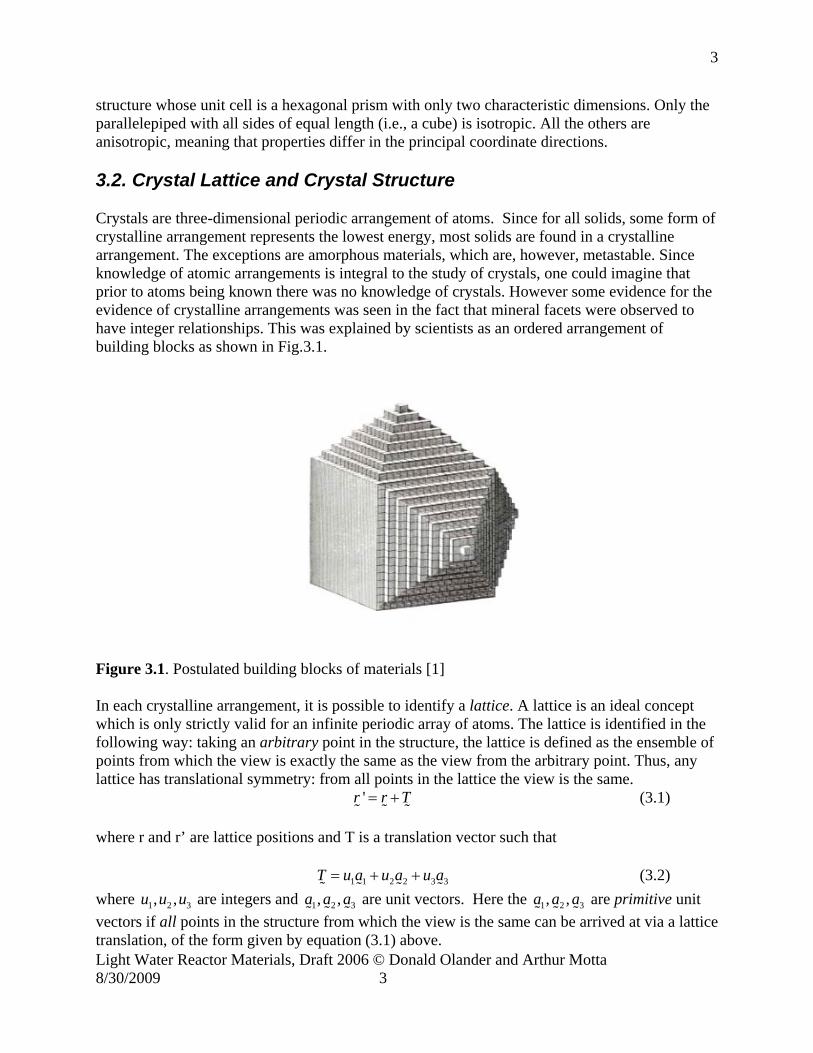
Crystals are three-dimensional periodic arrangement of atoms. Since for all solids, some form of crystalline arrangement represents the lowest energy, most solids are found in a crystalline arrangement. The exceptions are amorphous materials, which are, however, metastable. Since knowledge of atomic arrangements is integral to the study of crystals, one could imagine that prior to atoms being known there was no knowledge of crystals. However some evidence for the evidence of crystalline arrangements was seen in the fact that mineral facets were observed to have integer relationships. This was explained by scientists as an ordered arrangement of building blocks as shown in Fig.3.1.
Figure 3.1. Postulated building blocks of materials [1] In each crystalline arrangement, it is possible to identify a lattice. A lattice is an ideal concept which is only strictly valid for an infinite periodic array of atoms. The lattice is identified in the following way: taking an arbitrary point in the structure, the lattice is defined as the ensemble of points from which the view is exactly the same as the view from the arbitrary point. Thus, any lattice has translational symmetry: from all points in the lattice the view is the same. 'r r T= + (3.1) where r and r’ are lattice positions and T is a translation vector such that 1 1 2 2 3 3T u a u a u a= + +
Light Water Reactor Materials, Draft 2006 © Donald Olander and Arthur Motta
where are integers and are unit vectors. Here the are primitive unit vectors if all points in the structure from which the view is the same can be arrived at via a lattice translation, of the form given by equation
(3.2)
1 2 3, ,u u u 1 2 3, ,a a a 1 2 3, ,a a a
(3.1) above.
8/30/2009 3
4
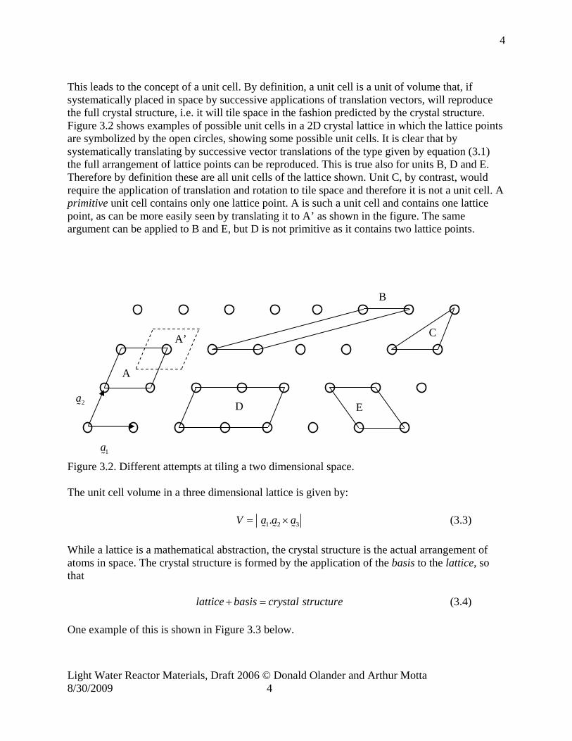
This leads to the concept of a unit cell. By definition, a unit cell is a unit of volume that, if systematically placed in space by successive applications of translation vectors, will reproduce the full crystal structure, i.e. it will tile space in the fashion predicted by the crystal structure. Figure 3.2 shows examples of possible unit cells in a 2D crystal lattice in which the lattice points are symbolized by the open circles, showing some possible unit cells. It is clear that by systematically translating by successive vector translations of the type given by equation (3.1) the full arrangement of lattice points can be reproduced. This is true also for units B, D and E. Therefore by definition these are all unit cells of the lattice shown. Unit C, by contrast, would require the application of translation and rotation to tile space and therefore it is not a unit cell. A primitive unit cell contains only one lattice point. A is such a unit cell and contains one lattice point, as can be more easily seen by translating it to A’ as shown in the figure. The same argument can be applied to B and E, but D is not primitive as it contains two lattice points.
B
C A’
A
Light Water Reactor Materials, Draft 2006 © Donald Olander and Arthur Motta
Figure 3.2. Different attempts at tiling a two dimensional space.
1a
2a D E
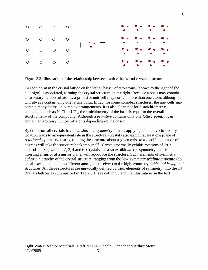
The unit cell volume in a three dimensional lattice is given by: 1 2 3.V a a a= × (3.3) While a lattice is a mathematical abstraction, the crystal structure is the actual arrangement of atoms in space. The crystal structure is formed by the application of the basis to the lattice, so that (3.4) lattice basis crystal structure+ = One example of this is shown in Figure 3.3 below.
8/30/2009 4
5
Light Water Reactor Materials, Draft 2006 © Donald Olander and Arthur Motta
Figure 3.3: Illustration of the relationship between lattice, basis and crystal structure To each point in the crystal lattice on the left a “basis” of two atoms, (shown to the right of the plus sign) is associated, forming the crystal structure on the right. Because a basis may contain an arbitrary number of atoms, a primitive unit cell may contain more than one atom, although it will always contain only one lattice point. In fact for some complex structures, the unit cells may contain many atoms, in complex arrangements. It is also clear that for a stoichiometric compound, such as NaCl or UO2, the stoichiometry of the basis is equal to the overall stoichiometry of the compound. Although a primitive contains only one lattice point, it can contain an arbitrary number of atoms depending on the basis.
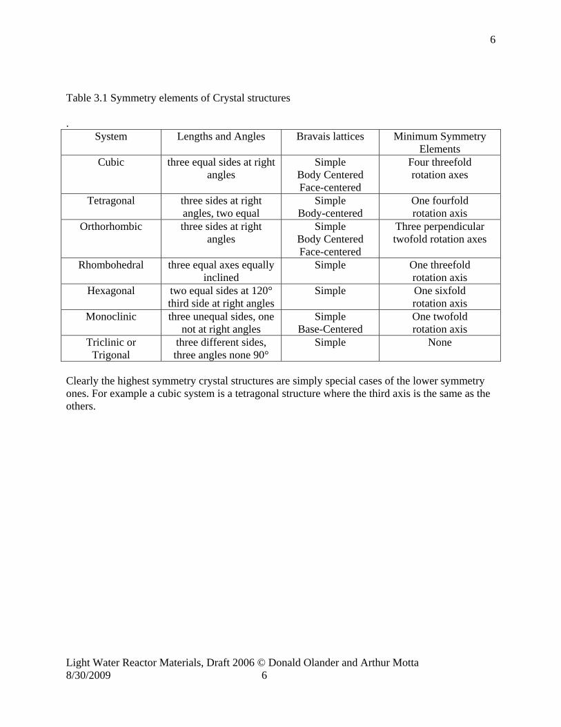
By definition all crystals have translational symmetry, that is, applying a lattice vector to any location leads to an equivalent site in the structure. Crystals also exhibit at least one plane of rotational symmetry, that is, rotating the structure about a given axis by a specified number of degrees will take the structure back into itself. Crystals normally exhibit rotations of 2π/n around an axis, with n= 2, 3, 4 and 6. Crystals can also exhibit mirror symmetry, that is, inserting a mirror at a mirror plane, will reproduce the structure. Such elements of symmetry define a hierarchy of the crystal structure, ranging from the low-symmetry triclinic structure (no equal axes and all angles different among themselves) to the high symmetry cubic and hexagonal structures. All these structures are univocally defined by their elements of symmetry, into the 14 Bravais lattices as summarized in Table 3.1 (see column 3 and the illustrations in the text).
8/30/2009 5
6
Table 3.1 Symmetry elements of Crystal structures .
System Lengths and Angles Bravais lattices Minimum Symmetry Elements
Cubic three equal sides at right angles
Simple Body Centered Face-centered
Four threefold rotation axes
Tetragonal three sides at right angles, two equal
Simple Body-centered
One fourfold rotation axis
Orthorhombic three sides at right angles
Simple Body Centered Face-centered
Three perpendicular twofold rotation axes
Rhombohedral three equal axes equally inclined
Simple One threefold rotation axis
Hexagonal two equal sides at 120° third side at right angles
Simple One sixfold rotation axis
Monoclinic three unequal sides, one not at right angles
Simple Base-Centered
One twofold rotation axis
Triclinic or Trigonal
three different sides, three angles none 90°
Simple None
Clearly the highest symmetry crystal structures are simply special cases of the lower symmetry ones. For example a cubic system is a tetragonal structure where the third axis is the same as the others.
Light Water Reactor Materials, Draft 2006 © Donald Olander and Arthur Motta 8/30/2009 6
7
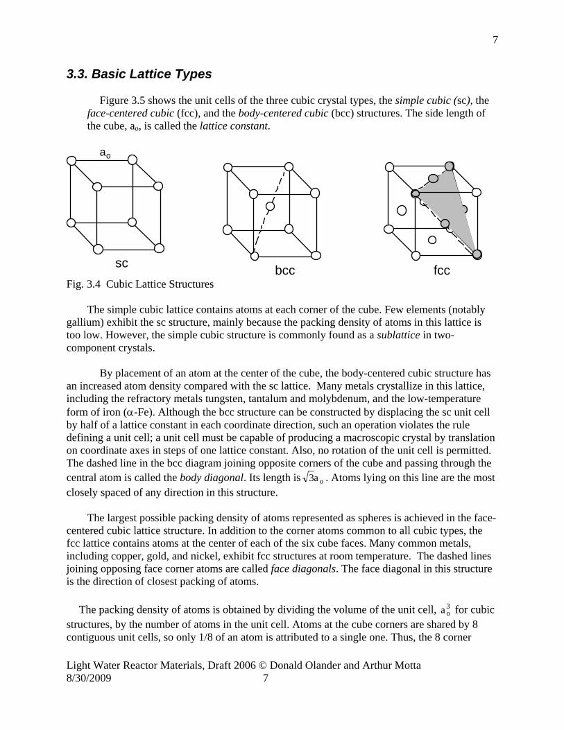
3.3. Basic Lattice Types
Figure 3.5 shows the unit cells of the three cubic crystal types, the simple cubic (sc), the face-centered cubic (fcc), and the body-centered cubic (bcc) structures. The side length of the cube, ao, is called the lattice constant.
Fig. 3.4 Cubic Lattice Structures
ao
sc bcc fcc
The simple cubic lattice contains atoms at each corner of the cube. Few elements (notably
gallium) exhibit the sc structure, mainly because the packing density of atoms in this lattice is too low. However, the simple cubic structure is commonly found as a sublattice in two-component crystals.
By placement of an atom at the center of the cube, the body-centered cubic structure has
an increased atom density compared with the sc lattice. Many metals crystallize in this lattice, including the refractory metals tungsten, tantalum and molybdenum, and the low-temperature form of iron (α-Fe). Although the bcc structure can be constructed by displacing the sc unit cell by half of a lattice constant in each coordinate direction, such an operation violates the rule defining a unit cell; a unit cell must be capable of producing a macroscopic crystal by translation on coordinate axes in steps of one lattice constant. Also, no rotation of the unit cell is permitted. The dashed line in the bcc diagram joining opposite corners of the cube and passing through the central atom is called the body diagonal. Its length is oa3 . Atoms lying on this line are the most closely spaced of any direction in this structure.
The largest possible packing density of atoms represented as spheres is achieved in the face-
centered cubic lattice structure. In addition to the corner atoms common to all cubic types, the fcc lattice contains atoms at the center of each of the six cube faces. Many common metals, including copper, gold, and nickel, exhibit fcc structures at room temperature. The dashed lines joining opposing face corner atoms are called face diagonals. The face diagonal in this structure is the direction of closest packing of atoms.
The packing density of atoms is obtained by dividing the volume of the unit cell, for cubic
structures, by the number of atoms in the unit cell. Atoms at the cube corners are shared by 8 contiguous unit cells, so only 1/8 of an atom is attributed to a single one. Thus, the 8 corner
3oa
Light Water Reactor Materials, Draft 2006 © Donald Olander and Arthur Motta 8/30/2009 7
8
Light Water Reactor Materials, Draft 2006 © Donald Olander and Arthur Motta
3oa 3
o3o
atoms in the cubic structures provide one effective atom to a unit cell. The atom in the center of the bcc structure belongs exclusively to the unit cell in which it resides. The face-centered atoms in the fcc structure are shared between adjacent unit cells, and so contribute one half an atom to each. With these rules, the atomic volumes (atoms per unit volume) of the three cubic structures are for the sc, a /2 for the bcc, and a /4 for the fcc.
Another important geometric feature of a crystal structure is the nearest distance between
atom centers (often called the nearest-neighbor distance). This distance is ao for the sc lattice, 2/a3 o (half of a body diagonal) in the bcc lattice, and 2/a o (half of a face diagonal) for the
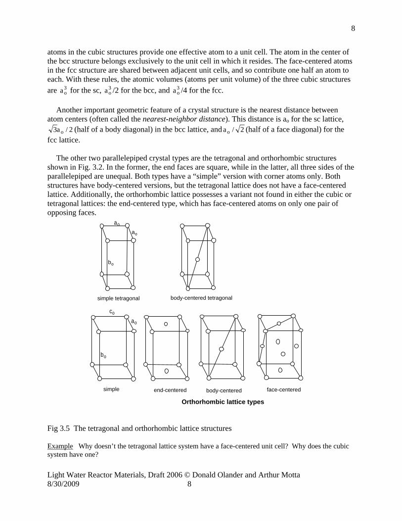
fcc lattice. The other two parallelepiped crystal types are the tetragonal and orthorhombic structures
shown in Fig. 3.2. In the former, the end faces are square, while in the latter, all three sides of the parallelepiped are unequal. Both types have a “simple” version with corner atoms only. Both structures have body-centered versions, but the tetragonal lattice does not have a face-centered lattice. Additionally, the orthorhombic lattice possesses a variant not found in either the cubic or tetragonal lattices: the end-centered type, which has face-centered atoms on only one pair of opposing faces.
simple tetragonal body-centered tetragonal
ao
bo
ao
bo
ao
co
simple end-centered body-centered face-centered
Orthorhombic lattice types
Fig 3.5 The tetragonal and orthorhombic lattice structures
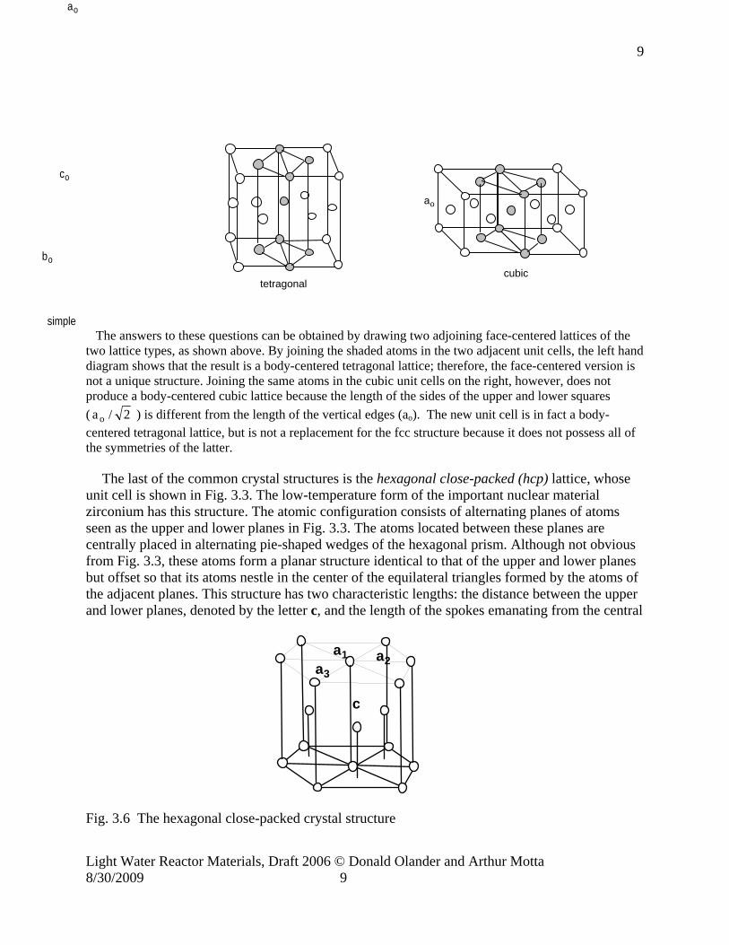
Example Why doesn’t the tetragonal lattice system have a face-centered unit cell? Why does the cubic system have one?
8/30/2009 8
9
bo
co
simple
ao
tetragonalcubic
ao
The answers to these questions can be obtained by drawing two adjoining face-centered lattices of the two lattice types, as shown above. By joining the shaded atoms in the two adjacent unit cells, the left hand diagram shows that the result is a body-centered tetragonal lattice; therefore, the face-centered version is not a unique structure. Joining the same atoms in the cubic unit cells on the right, however, does not produce a body-centered cubic lattice because the length of the sides of the upper and lower squares ( 2/a o ) is different from the length of the vertical edges (ao). The new unit cell is in fact a body-centered tetragonal lattice, but is not a replacement for the fcc structure because it does not possess all of the symmetries of the latter.
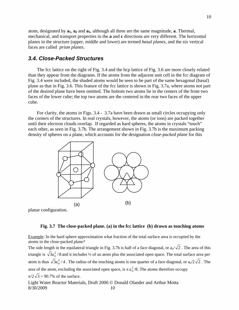
The last of the common crystal structures is the hexagonal close-packed (hcp) lattice, whose unit cell is shown in Fig. 3.3. The low-temperature form of the important nuclear material zirconium has this structure. The atomic configuration consists of alternating planes of atoms seen as the upper and lower planes in Fig. 3.3. The atoms located between these planes are centrally placed in alternating pie-shaped wedges of the hexagonal prism. Although not obvious from Fig. 3.3, these atoms form a planar structure identical to that of the upper and lower planes but offset so that its atoms nestle in the center of the equilateral triangles formed by the atoms of the adjacent planes. This structure has two characteristic lengths: the distance between the upper and lower planes, denoted by the letter c, and the length of the spokes emanating from the central
a1 a2a3
c
Fig. 3.6 The hexagonal close-packed crystal structure
Light Water Reactor Materials, Draft 2006 © Donald Olander and Arthur Motta 8/30/2009 9
10
atom, designated by a1, a2 and a3, although all three are the same magnitude, a. Thermal, mechanical, and transport properties in the a and c directions are very different. The horizontal planes in the structure (upper, middle and lower) are termed basal planes, and the six vertical faces are called prism planes. 3.4. Close-Packed Structures
The fcc lattice on the right of Fig. 3.4 and the hcp lattice of Fig. 3.6 are more closely related than they appear from the diagrams. If the atoms from the adjacent unit cell in the fcc diagram of Fig. 3.4 were included, the shaded atoms would be seen to be part of the same hexagonal (basal) plane as that in Fig. 3.6. This feature of the fcc lattice is shown in Fig. 3.7a, where atoms not part of the desired plane have been omitted. The bottom two atoms lie in the centers of the front two faces of the lower cube; the top two atoms are the centered in the rear two faces of the upper cube.
For clarity, the atoms in Figs. 3.4 - 3.7a have been drawn as small circles occupying only
the corners of the structures. In real crystals, however, the atoms (or ions) are packed together until their electron clouds overlap. If regarded as hard spheres, the atoms in crystals “touch” each other, as seen in Fig. 3.7b. The arrangement shown in Fig. 3.7b is the maximum packing density of spheres on a plane, which accounts for the designation close-packed plane for this
planar configuration. (a) (b)
Fig. 3.7 The close-packed plane. (a) in the fcc lattice (b) drawn as touching atoms
Example: In the hard sphere approximation what fraction of the total surface area is occupied by the atoms in the close-packed plane? The side length in the equilateral triangle in Fig. 3.7b is half of a face diagonal, or ao/ 2 . The area of this triangle is 8/a3 2
o and it includes ½ of an atom plus the associated open space. The total surface area per
atom is thus 4/a3 2o . The radius of the touching atoms is one quarter of a face diagonal, or ao/2 2 . The
area of the atom, excluding the associated open space, is π /8. The atoms therefore occupy 2oa
π/2 3 = 90.7% of the surface. Light Water Reactor Materials, Draft 2006 © Donald Olander and Arthur Motta 8/30/2009 10
11
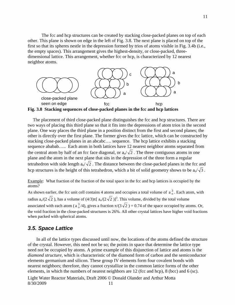
The fcc and hcp structures can be created by stacking close-packed planes on top of each other. This plane is shown on edge in the left of Fig. 3.8. The next plane is placed on top of the first so that its spheres nestle in the depression formed by trios of atoms visible in Fig. 3.4b (i.e., the empty spaces). This arrangement gives the highest-density, or close-packed, three-dimensional lattice. This arrangement, whether fcc or hcp, is characterized by 12 nearest neighbor atoms.
a
b
c
a
b
a
fcc hcpclose-packed planeseen on edge
Fig. 3.8 Stacking sequences of close-packed planes in the fcc and hcp lattices The placement of third close-packed plane distinguishes the fcc and hcp structures. There are
two ways of placing this third plane so that it fits into the depressions of atom trios in the second plane. One way places the third plane in a position distinct from the first and second planes; the other is directly over the first plane. The former gives the fcc lattice, which can be constructed by stacking close-packed planes in an abcabc…. sequence. The hcp lattice exhibits a stacking sequence ababab….. Each atom in both lattices have 12 nearest neighbor atoms separated from the central atom by half of an fcc face diagonal, or ao/ 2 . The three contiguous atoms in one plane and the atom in the next plane that sits in the depression of the three form a regular tetrahedron with side length ao/ 2 . The distance between the close-packed planes in the fcc and hcp structures is the height of this tetrahedron, which a bit of solid geometry shows to be ao/ 3 .
Example: What fraction of the fraction of the total space in the fcc and hcp lattices is occupied by the atoms? As shown earlier, the fcc unit cell contains 4 atoms and occupies a total volume of . Each atom, with radius ao/(2
3oa
2 ), has a volume of (4/3)π[ ao/(2 2 )]3. This volume, divided by the total volume associated with each atom ( /4), gives a fraction π/(33
oa 2 ) = 0.74 of the space occupied by atoms. Or, the void fraction in the close-packed structures is 26%. All other crystal lattices have higher void fractions when packed with spherical atoms. 3.5. Space Lattice
In all of the lattice types discussed until now, the locations of the atoms defined the structure of the crystal. However, this need not be so; the points in space that determine the lattice type need not be occupied by atoms. A prime example of this disjunction of lattice and atoms is the diamond structure, which is characteristic of the diamond form of carbon and the semiconductor elements germanium and silicon. These group IV elements form four covalent bonds with nearest neighbors; therefore, they cannot crystallize in the common lattice forms of the other elements, in which the numbers of nearest neighbors are 12 (fcc and hcp), 8 (bcc) and 6 (sc). Light Water Reactor Materials, Draft 2006 © Donald Olander and Arthur Motta 8/30/2009 11
12
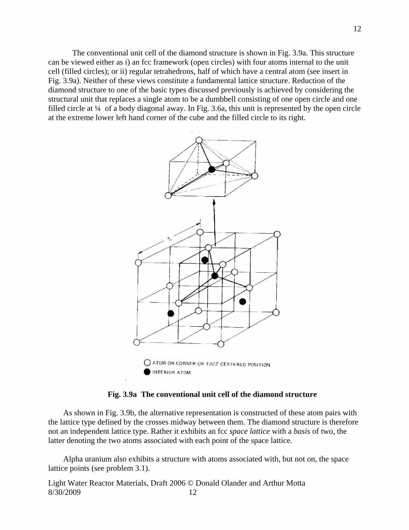
The conventional unit cell of the diamond structure is shown in Fig. 3.9a. This structure can be viewed either as i) an fcc framework (open circles) with four atoms internal to the unit cell (filled circles); or ii) regular tetrahedrons, half of which have a central atom (see insert in Fig. 3.9a). Neither of these views constitute a fundamental lattice structure. Reduction of the diamond structure to one of the basic types discussed previously is achieved by considering the structural unit that replaces a single atom to be a dumbbell consisting of one open circle and one filled circle at ¼ of a body diagonal away. In Fig. 3.6a, this unit is represented by the open circle at the extreme lower left hand corner of the cube and the filled circle to its right.
Fig. 3.9a The conventional unit cell of the diamond structure
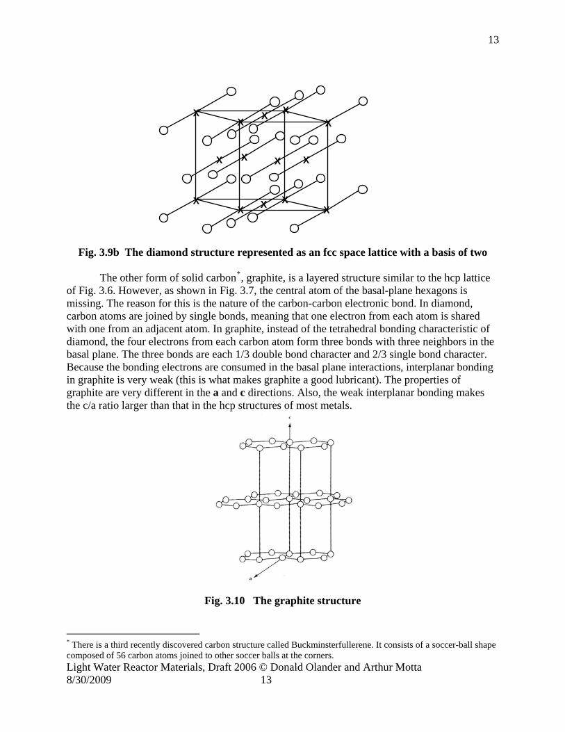
As shown in Fig. 3.9b, the alternative representation is constructed of these atom pairs with the lattice type defined by the crosses midway between them. The diamond structure is therefore not an independent lattice type. Rather it exhibits an fcc space lattice with a basis of two, the latter denoting the two atoms associated with each point of the space lattice.
Alpha uranium also exhibits a structure with atoms associated with, but not on, the space
lattice points (see problem 3.1).
Light Water Reactor Materials, Draft 2006 © Donald Olander and Arthur Motta 8/30/2009 12
13
X
X
X
XX
X
XX
X
X
X X
X
X
Fig. 3.9b The diamond structure represented as an fcc space lattice with a basis of two
The other form of solid carbon*, graphite, is a layered structure similar to the hcp lattice of Fig. 3.6. However, as shown in Fig. 3.7, the central atom of the basal-plane hexagons is missing. The reason for this is the nature of the carbon-carbon electronic bond. In diamond, carbon atoms are joined by single bonds, meaning that one electron from each atom is shared with one from an adjacent atom. In graphite, instead of the tetrahedral bonding characteristic of diamond, the four electrons from each carbon atom form three bonds with three neighbors in the basal plane. The three bonds are each 1/3 double bond character and 2/3 single bond character. Because the bonding electrons are consumed in the basal plane interactions, interplanar bonding in graphite is very weak (this is what makes graphite a good lubricant). The properties of graphite are very different in the a and c directions. Also, the weak interplanar bonding makes the c/a ratio larger than that in the hcp structures of most metals.
Fig. 3.10 The graphite structure
Light Water Reactor Materials, Draft 2006 © Donald Olander and Arthur Motta
* There is a third recently discovered carbon structure called Buckminsterfullerene. It consists of a soccer-ball shape composed of 56 carbon atoms joined to other soccer balls at the corners.
8/30/2009 13
14
3.6. Miller indices
Discussion of the properties of crystalline solids requires a method of identifying atomic planes and directions the the lattice. The term “close-packed” has been used to describe the atomic planes in Figs 3.7 and 3.8. However, there are many more planes in the various structures, and word descriptions of these are obviously impossible. Similarly, the terms “body diagonal” and “face diagonal” have been applied to directions in cubic crystals. Designating the many other directions calls for a more concise labeling technique.
A general method for designating planes starts with a coordinate system whose unit vectors a, b, and c (called crystal axes) are equal to the lengths of the sides of the unit cell and point in the directions of these sides. The recipe for designating a plane is as follows:
1. Pick an origin at a lattice point that is not in the plane to be designated 2. From this origin, draw the crystal axes. Determine how many multiples of the unit lengths of
these vectors are required to reach the plane in question. These multiples are designated as fa, fb, and fc.
3. Take the reciprocals , 1c
1b
1a f,f,f −−−
4. Reduce the reciprocals to the set of smallest integers and enclose them in parentheses (ijk). This is the Miller index of the plane.
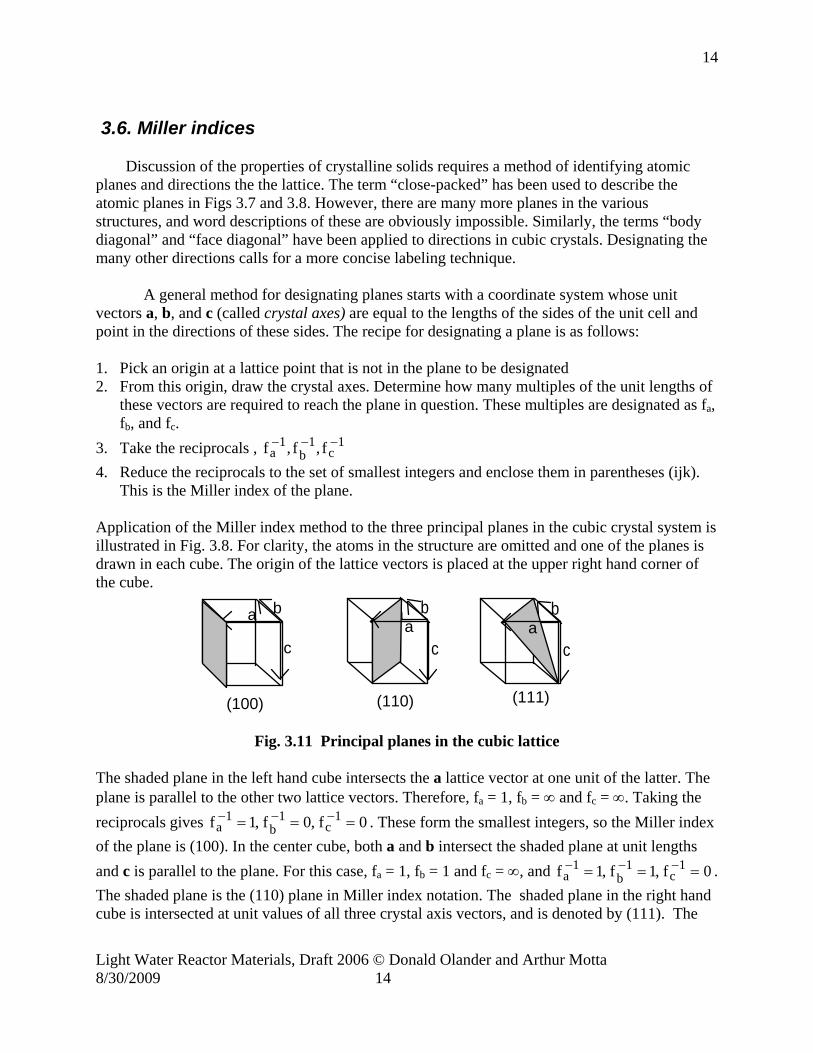
Application of the Miller index method to the three principal planes in the cubic crystal system is illustrated in Fig. 3.8. For clarity, the atoms in the structure are omitted and one of the planes is drawn in each cube. The origin of the lattice vectors is placed at the upper right hand corner of the cube.
a b
c
a b
ca a b
ca
(100) (110) (111)
Fig. 3.11 Principal planes in the cubic lattice The shaded plane in the left hand cube intersects the a lattice vector at one unit of the latter. The plane is parallel to the other two lattice vectors. Therefore, fa = 1, fb = ∞ and fc = ∞. Taking the reciprocals gives 0f,0f,1f 1
c1
b1
a === −−− . These form the smallest integers, so the Miller index of the plane is (100). In the center cube, both a and b intersect the shaded plane at unit lengths and c is parallel to the plane. For this case, fa = 1, fb = 1 and fc = ∞, and 0f,1f,1f 1
c1
b1
a === −−− . The shaded plane is the (110) plane in Miller index notation. The shaded plane in the right hand cube is intersected at unit values of all three crystal axis vectors, and is denoted by (111). The
Light Water Reactor Materials, Draft 2006 © Donald Olander and Arthur Motta 8/30/2009 14
15
Miller indices of the planes in Fig. 3.11 apply to the sc, bcc, and fcc structures in the cubic system.
The system employing three crystal axis vectors can be applied to any lattice type. For the hexagonal structure, however, the Miller index system is slightly modified to reflect the hexagonal symmetries of this lattice. In addition to the c axis, three other unit vectors are adopted, namely a1, a2 and a3 in Fig. 3.6. The indexing method is identical to that described above for the cubic system except for the inclusion of a redundant unit vector. Taking the origin at the center of the bottom hexagon in Fig. 3.6, the intersections of the upper hexagon with the unit vectors is . Taking reciprocals, the Miller index of the
basal plane is (0001). Starting from the front plane in Fig. 3.6 and moving clockwise, the six prism planes in the hexagonal structure are (
1f,f,f,f caaa 321=∞=∞=∞=
1 010), (0 1 10), (1 1 00), (10 1 0), (01 1 0) and ( 1 100). The notation 1 means –1, which results from the Miller index recipe when the unit vector points away from the plane to be designated. The general Miller index for the hexagonal structure is (hkil). To account for the extra lattice vector, h + k + i = 0.
A modified version of the Miller index method for naming planes is applicable to
designating directions in a crystal. From an origin on a lattice point, the line is drawn in the desired direction and terminates at an arbitrary point, whose coordinates are described as na, nb and nc multiples of the lattice vectors. These numbers are reduced to the lowest set of integers i, j, and k, and enclosed in brackets to give the Miller index for the direction as [hkl] (or [hkil] for hexagonal lattices)
Example: What are the directions perpendicular to the shaded planes in Fig. 3.11? The origin is chosen as top front right hand corner of the cubes. From this origin, the line perpendicular to the (100) plane in the first cube is coincident with the a lattice vector. The end point is chosen as the intersection of this direction with the (100) plane. The coordinates of this point are na = 1, nb = 0, nc = 0, so the direction is [100]. Using the same origin, the direction perpendicular to the (110) plane in the center cube is one half of a face diagonal. The intersection of this plane with the face diagonal occurs at lattice vector units of na = ½ , nb = ½ and nc = 0. Multiplying by two to convert to integers gives the Miller index of [110]. This is the direction of the face diagonal in the cubic system The perpendicular to the (111) plane in the right hand cube in Fig. 3.11 is the body diagonal starting from the origin. A bit of trigonometry shows that the intersection of the body diagonal with the shaded (111) plane occurs at a point with the coordinates na = nb = nc = 1/3. Consequently, the Miller index of the body diagonal in the cubic lattice is [111]. To find this direction, it was not necessary to terminate the line on the (111) plane. Had the line been continued to the opposite corner of the cube, the coordinates would have been na = nb = nc = 1, giving the same result for the Miller index. The above example suggests the general rule: In cubic crystals, directions and the planes perpendicular to them have the same Miller indices. The same rule applies to the hexagonal lattice, as can be demonstrated by applying the Miller index recipe for directions to lines perpendicular to the prism and basal planes in Fig. 3.6. The rule for relating the Miller indices of directions with those of the planes perpendicular to them does not apply to the tetragonal or orthorhombic crystal structures, or any other lattice types with lower degrees of symmetry.
Light Water Reactor Materials, Draft 2006 © Donald Olander and Arthur Motta 8/30/2009 15
16
3.6.1. Distances between planes The distance between crystal planes is the quantity most often measured using x-ray diffraction to determine crystal structure. From inspection it is apparent that in the cubic crystal the distance between successive (100) planes is simply ao. These are the most widely spaced planes (and conversely those with the highest atomic density) in the structure. The distance between 110 planes can also be visualized by looking at the cube from the z direction, where it is found that it is one half the face diagonal or ao/2. In general for cubic lattices
2 2 2
ohkl
adh k l
=+ +
(3.5)
The angles between directions are also of interest. for the cubic system the angle between h1k1l1 and h2k2l2 is
1 1 2 1 2 1 22 2 2 2 2 2
1 1 1 2 2 2
cos( )( )
h h k k l lh k l h k l
φ −⎡ ⎤+ +⎢=⎢ ⎥+ + + +⎣ ⎦
⎥ (3.6)
for the other systems the interplanar distances and formulas can be found in [2].
3.7. Ionic solids
Many technologically-important solids consist of two elements. Naturally-occurring
minerals often contain three or more elements. The two-component solids consist of combinations of electropositive elements from the left side of the periodic table and electronegative elements from the right side. Because as neutral elements, former the possess 1 –3 electrons in their outer electron shell and the latter lack 1 or 2 electrons in their outermost orbital, transfer of the electrons between the two species is energetically favorable. The resulting compound consists of positive ions called cations (M) and negative ions termed anions (X). Both the formula of these ionic solids, MjXk, and their crystal structures are determined by the charges (valences) of the cations and anions.
The crystal structures of two-component ionic solids is best viewed as interlaced
sublattices of cations and anions. Each sublattice is one of the simple types treated earlier in this chapter. For minimum crystal energy, the structures are restricted to those in which all cation nearest neighbors are anions and vice versa. This condition maximizes the Coulomb attraction of the two oppositely-charged species. The lattice type is named for a common compound that exhibits the particular structure. The NaCl structure is shown in the left hand diagram of Fig. 3.12. This lattice type consists of two intermingled sublattices of the fcc type, and is characteristic of cations and anions of the same valence. Examples of this structure include LiH (unit valence cation and anion), MnO(divalent ions) and UC (tetravalent elements).
Light Water Reactor Materials, Draft 2006 © Donald Olander and Arthur Motta 8/30/2009 16
17
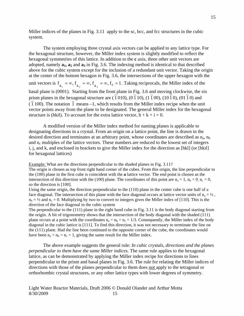
NaCl structure CsCl structure
Fig 3.12 Lattices formed by compounds of equal valence ions
The other common lattice formed by compounds with equal-valence cations and anions is the CsCl structure depicted on the right of Fig. 3.12. This structure consists of two interlaced simple cubic sublattices. Whether an MX solid exhibits the NaCl or CsCl structure depends on the relative sizes of the anions and cations and on the interatomic forces responsible for formation of the solid.
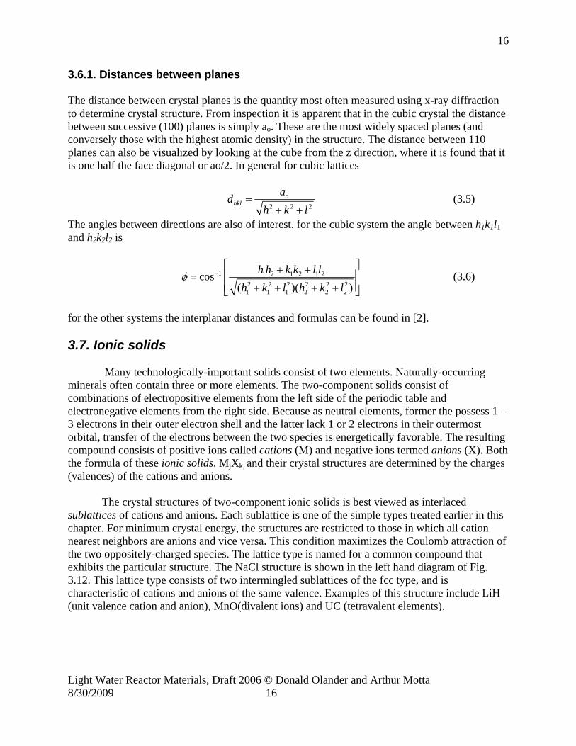
The nuclear fuel uranium dioxide (UO2) crystallizes in the fluorite structure, named after
the earlier prototype CaCl2, a naturally occurring mineral. In this ionic solid, the cation valence is twice the anion valence. Two views of this structure are shown in Fig. 3.13. The U4+ ions form
Fig. 3.13 The Fluorite structure of UO2 an fcc sublattice that meshes with a simple cubic O2- sublattice. The left hand version shows that U4+ ions occupy every other cube formed by the anions. The right hand drawing shows the structures of the two sublattices more clearly. One of the major advantages of UO2 as a nuclear fuel is the stability of its fluorite structure up to the melting point of 2860oC. The oxygen ions that accord UO2 its great stability serve no nuclear purpose. However, they occupy space and result in the undesirable low uranium density of UO2, which is one-half that of U metal.
Light Water Reactor Materials, Draft 2006 © Donald Olander and Arthur Motta 8/30/2009 17
18
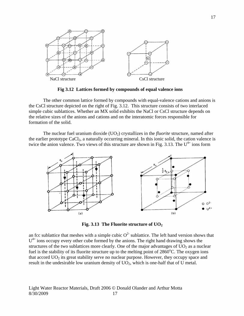
The third common binary crystal type is the corundum, named after its best-known representative, alumina. Corundum lattices are restricted to compounds with the generic stoichiometry M2O3. These compounds are also called sesquioxides. The cation valence is always 3+. The basic feature of this lattice are the large O2- ions, which form an hcp structure of the type shown in Fig. 3.6. Figure 3.14 shows one basal plane of the corundum lattice viewed along the c axis. The superimposed hexagons highlight this familiar pattern. Placement of the Al3+ ions in this plane can be viewed in two ways. First, the cations occupy two-thirds of the interstices in the close-packed O2- plane; second, the cations form a hexagonal basal plane of the graphite structure (Fig. 3.10).
Al3+
O2-
Light Water Reactor Materials, Draft 2006 © Donald Olander and Arthur Motta
Fig. 3.14 Top view of the corundum unit cell
unit cell ontains three oxygen ions. The stoichiometry of the crystal is thus Al O , as required.
d occupy sequentially the six possible adjoining
terstitial positions in the hexagon of anions.
e-earth products of uranium fission in UO2 (La2 3, Nd2O3, etc), also form this crystal structure.
3.8. Experimental determination of the crystal structure
f
The hexagons drawn in Fig. 3.14 can be regarded as two-dimensional unit cells of the corundum structure. Each hexagon contains two Al3+ entirely within its boundary. Each of the six anions that form the periphery of the hexagons are shared among three such units, so that two peripheral O2- are assigned to each hexagon. Together with the central anion, the planarc 2 3 The complete three-dimensional unit cell of corundum contains six close-packed O2- planes arranged in the stacking sequence of the hcp lattice. Each of these planes is differentiateby the placement of the pairs of cations, whichin In addition to Al2O3, the corrosion products of steel, Cr2O3 and Fe2O3, exhibit the corundum lattice structure. In their pure states, the rar
O
Our knowledge of the crystal structure of materials comes mainly from the coherent scattering oelectromagnetic radiation in the form of x-rays from these materials. Bragg’s law of diffraction
8/30/2009 18
19
Light Water Reactor Materials, Draft 2006 © Donald Olander and Arthur Motta
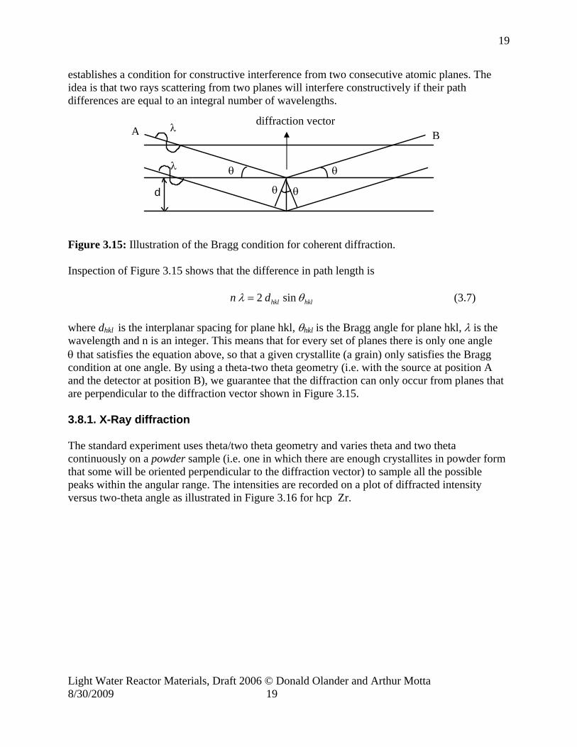
The constructively if their path
ifferences are equal to an integral number of wavelengths.
establishes a condition for constructive interference from two consecutive atomic planes.idea is that two rays scattering from two planes will interfered
θ θ
θθd
λ
λ
diffraction vector A B
Figure 3.15: Illustration of the Bragg condition for coherent diffraction.
spection of Figure 3.15 shows that the difference in path length is In 2 sinhkl hkln dλ θ= (3.7)
n only occur from planes that re perpendicular to the diffraction vector shown in Figure 3.15.
.8.1. X-Ray diffraction
orm
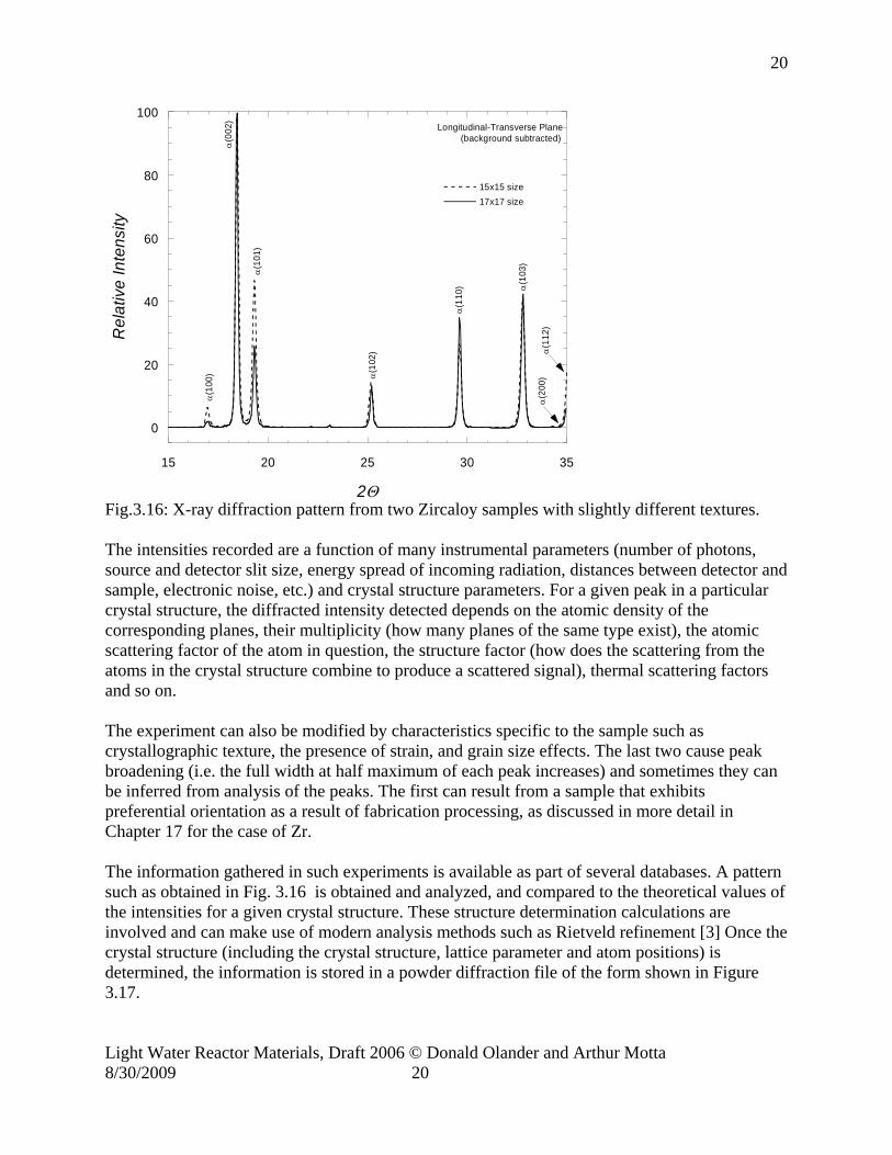
plot of diffracted intensity ersus two-theta angle as illustrated in Figure 3.16 for hcp Zr.
where dhkl is the interplanar spacing for plane hkl, θhkl is the Bragg angle for plane hkl, λ is thewavelength and n is an integer. This means that for every set of planes there is only one angle θ that satisfies the equation above, so that a given crystallite (a grain) only satisfies the Bragg condition at one angle. By using a theta-two theta geometry (i.e. with the source at position A and the detector at position B), we guarantee that the diffraction caa 3 The standard experiment uses theta/two theta geometry and varies theta and two theta continuously on a powder sample (i.e. one in which there are enough crystallites in powder fthat some will be oriented perpendicular to the diffraction vector) to sample all the possible peaks within the angular range. The intensities are recorded on av
8/30/2009 19
20
0
20
40
60
80
100
15 20 25 30 35
15x15 size17x17 size
Rel
ativ
e In
tens
ity
2Θ
α(1
00)
Longitudinal-Transverse Plane(background subtracted)
α(0
02)
α(1
01)
α(1
10)
α(1
02)
α(1
03)
α(2
00)
α(1
12)
Fig.3.16: X-ray diffraction pattern from two Zircaloy samples with slightly different textures. The intensities recorded are a function of many instrumental parameters (number of photons, source and detector slit size, energy spread of incoming radiation, distances between detector and sample, electronic noise, etc.) and crystal structure parameters. For a given peak in a particular crystal structure, the diffracted intensity detected depends on the atomic density of the corresponding planes, their multiplicity (how many planes of the same type exist), the atomic scattering factor of the atom in question, the structure factor (how does the scattering from the atoms in the crystal structure combine to produce a scattered signal), thermal scattering factors and so on. The experiment can also be modified by characteristics specific to the sample such as crystallographic texture, the presence of strain, and grain size effects. The last two cause peak broadening (i.e. the full width at half maximum of each peak increases) and sometimes they can be inferred from analysis of the peaks. The first can result from a sample that exhibits preferential orientation as a result of fabrication processing, as discussed in more detail in Chapter 17 for the case of Zr. The information gathered in such experiments is available as part of several databases. A pattern such as obtained in Fig. 3.16 is obtained and analyzed, and compared to the theoretical values of the intensities for a given crystal structure. These structure determination calculations are involved and can make use of modern analysis methods such as Rietveld refinement [3] Once the crystal structure (including the crystal structure, lattice parameter and atom positions) is determined, the information is stored in a powder diffraction file of the form shown in Figure 3.17.
Light Water Reactor Materials, Draft 2006 © Donald Olander and Arthur Motta 8/30/2009 20
21
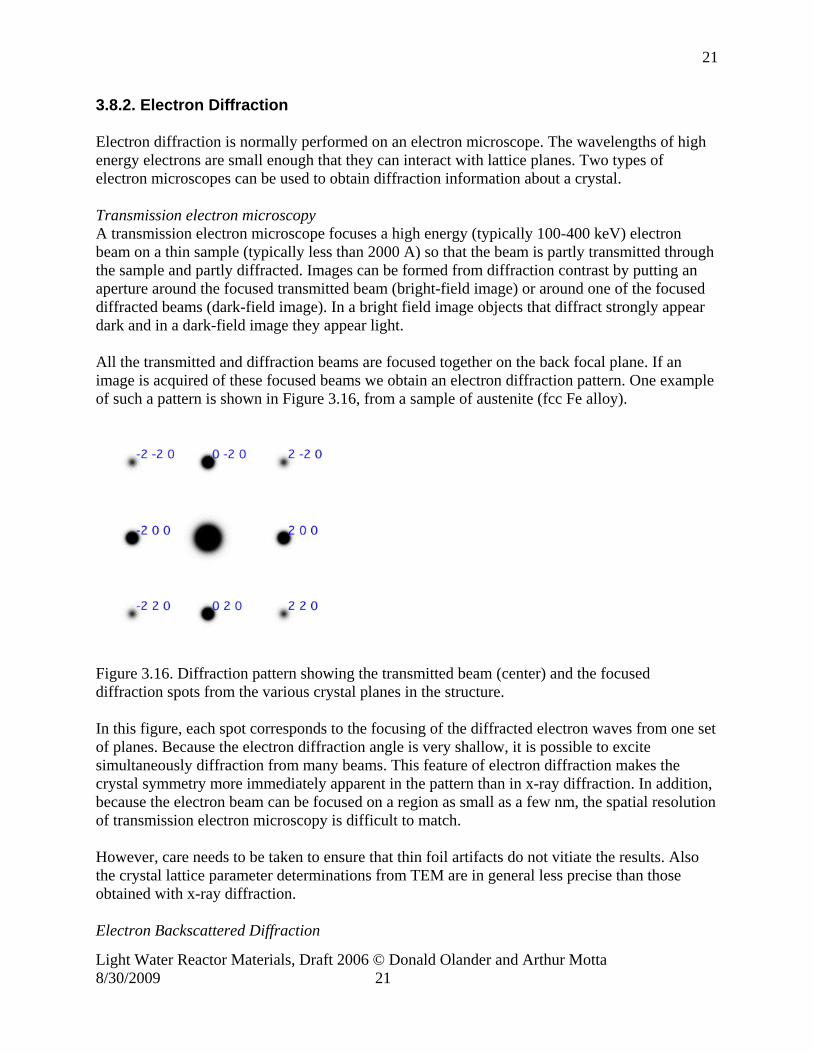
3.8.2. Electron Diffraction Electron diffraction is normally performed on an electron microscope. The wavelengths of high energy electrons are small enough that they can interact with lattice planes. Two types of electron microscopes can be used to obtain diffraction information about a crystal. Transmission electron microscopy A transmission electron microscope focuses a high energy (typically 100-400 keV) electron beam on a thin sample (typically less than 2000 A) so that the beam is partly transmitted through the sample and partly diffracted. Images can be formed from diffraction contrast by putting an aperture around the focused transmitted beam (bright-field image) or around one of the focused diffracted beams (dark-field image). In a bright field image objects that diffract strongly appear dark and in a dark-field image they appear light. All the transmitted and diffraction beams are focused together on the back focal plane. If an image is acquired of these focused beams we obtain an electron diffraction pattern. One example of such a pattern is shown in Figure 3.16, from a sample of austenite (fcc Fe alloy).
Figure 3.16. Diffraction pattern showing the transmitted beam (center) and the focused diffraction spots from the various crystal planes in the structure. In this figure, each spot corresponds to the focusing of the diffracted electron waves from one set of planes. Because the electron diffraction angle is very shallow, it is possible to excite simultaneously diffraction from many beams. This feature of electron diffraction makes the crystal symmetry more immediately apparent in the pattern than in x-ray diffraction. In addition, because the electron beam can be focused on a region as small as a few nm, the spatial resolution of transmission electron microscopy is difficult to match. However, care needs to be taken to ensure that thin foil artifacts do not vitiate the results. Also the crystal lattice parameter determinations from TEM are in general less precise than those obtained with x-ray diffraction. Electron Backscattered Diffraction
Light Water Reactor Materials, Draft 2006 © Donald Olander and Arthur Motta 8/30/2009 21
22
The technique of Electron Backscatttered diffraction, also called orientation imaging, allows diffraction information to be obtained with the scanning electron microscope. The orientation of individual grains can be identified from their diffraction patterns and a much more extensive survey performed of the orientation distribution of grains in a sample than would be possible with TEM. This allows the identification of grain to grain mis-orientations, strain partitioning between grains and its direct correlation with the SEM image.
Light Water Reactor Materials, Draft 2006 © Donald Olander and Arthur Motta 8/30/2009 22
23
Problems
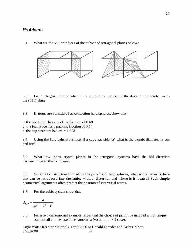
3.1. What are the Miller indices of the cubic and tetragonal planes below?
Light Water Reactor Materials, Draft 2006 © Donald Olander and Arthur Motta
3.2. For a tetragonal lattice where a=b=3c, find the indices of the direction perpendicular to the (011) plane. 3.3. If atoms are considered as contacting hard spheres, show that: a. the bcc lattice has a packing fraction of 0.68 b. the fcc lattice has a packing fraction of 0.74 c. the hcp structure has c/a = 1.633 3.4. Using the hard sphere premise, if a cube has side "a" what is the atomic diameter in bcc and fcc? 3.5. What low index crystal planes in the tetragonal systems have the hkl direction perpendicular to the hkl plane? 3.6. Given a bcc structure formed by the packing of hard spheres, what is the largest sphere that can be introduced into the lattice without distortion and where is it located? Such simple geometrical arguments often predict the position of interstitial atoms. 3.7. For the cubic system show that
d ah k lhkl =
+ +2 2 2
3.8. For a two dimensional example, show that the choice of primitive unit cell is not unique
but that all choices have the same area (volume for 3D case).
8/30/2009 23
24
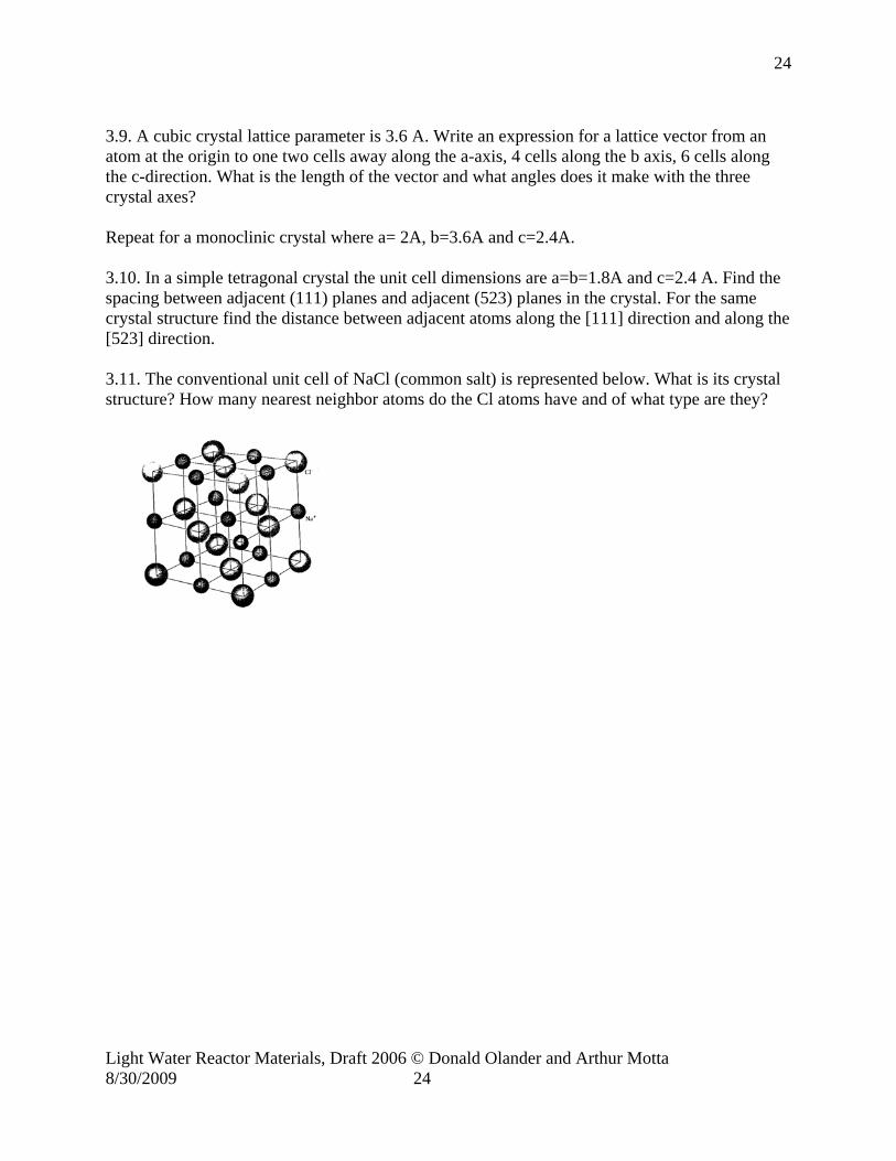
3.9. A cubic crystal lattice parameter is 3.6 A. Write an expression for a lattice vector from an atom at the origin to one two cells away along the a-axis, 4 cells along the b axis, 6 cells along the c-direction. What is the length of the vector and what angles does it make with the three crystal axes? Repeat for a monoclinic crystal where a= 2A, b=3.6A and c=2.4A. 3.10. In a simple tetragonal crystal the unit cell dimensions are a=b=1.8A and c=2.4 A. Find the spacing between adjacent (111) planes and adjacent (523) planes in the crystal. For the same crystal structure find the distance between adjacent atoms along the [111] direction and along the [523] direction. 3.11. The conventional unit cell of NaCl (common salt) is represented below. What is its crystal structure? How many nearest neighbor atoms do the Cl atoms have and of what type are they?
Light Water Reactor Materials, Draft 2006 © Donald Olander and Arthur Motta 8/30/2009 24
Light Water Reactor Materials, Draft 2006 © Donald Olander and Arthur Motta 8/30/2009 25
25
References [1] C. Kittel, Introduction to Solid State Physics, 6th edition: Wiley, 1986. [2] J. W. Edington, Practical Electron Microscopy in Materials Science, 1976. [3] R. A. Young, The Rietveld Method: Oxford: University Press, 1993.