Chapter 3 Control Unit - Home - IOE Notes · o It allows the execution of the microoperations...
23
Computer Organization and Architecture Chapter 3 : Control Unit Compiled By: Er. Hari Aryal [[email protected]] Reference: M. Mano & W. Stallings | 1 Chapter – 3 Control Unit 3.1 Control Memory The function of the control unit in a digital computer is to initiate sequences of microoperations. When the control signals are generated by hardware using conventional logic design techniques, the control unit is said to be hardwired. Microprogramming is a second alternative for designing the control unit of a digital computer. o The principle of microprogramming is an elegant and systematic method for controlling the microoperation sequences in a digital computer. In a bus-organized systems, the control signals that specify microoperations are groups of bits that select the paths in multiplexers, decoders, and arithmetic logic units. A control unit whose binary control variables are stored in memory is called a microprogrammed control unit. A memory that is part of a control unit is referred to as a control memory. o Each word in control memory contains within it a microinstruction. o A sequence of microinstructions constitutes a microprogram. o Can be either read-only memory(ROM) or writable control memory (dynamic microprogramming) A computer that employs a microprogrammed control unit will have two separate memories: o A main memory o A control memory The general configuration of a microprogrammed control unit is demonstrated in the block diagram of Fig. 3.1. o The control memory is assumed to be a ROM, within which all control information is permanently stored. o The control address register specifies the address of the microinstruction. o The control data register holds the microinstruction read from memory. Thus a microinstruction contains bits for initiating microoperations in the data processor part and bits that determine the address sequence for the control memory. Extra Stuff: Microprogram Program stored in memory that generates all the control signals required to execute the instruction set correctly Consists of microinstructions Microinstruction Contains a control word and a sequencing word Control Word - All the control information required for one clock cycle Sequencing Word - Information needed to decide the next microinstruction address Vocabulary to write a microprogram
Transcript of Chapter 3 Control Unit - Home - IOE Notes · o It allows the execution of the microoperations...

Computer Organization and Architecture Chapter 3 : Control Unit
Compiled By: Er. Hari Aryal [[email protected]] Reference: M. Mano & W. Stallings | 1
Chapter – 3
Control Unit 3.1 Control Memory
The function of the control unit in a digital computer is to initiate sequences of
microoperations.
When the control signals are generated by hardware using conventional logic design
techniques, the control unit is said to be hardwired.
Microprogramming is a second alternative for designing the control unit of a digital
computer.
o The principle of microprogramming is an elegant and systematic method for
controlling the microoperation sequences in a digital computer.
In a bus-organized systems, the control signals that specify microoperations are groups of
bits that select the paths in multiplexers, decoders, and arithmetic logic units.
A control unit whose binary control variables are stored in memory is called a
microprogrammed control unit.
A memory that is part of a control unit is referred to as a control memory.
o Each word in control memory contains within it a microinstruction.
o A sequence of microinstructions constitutes a microprogram.
o Can be either read-only memory(ROM) or writable control memory (dynamic
microprogramming)
A computer that employs a microprogrammed control unit will have two separate
memories:
o A main memory
o A control memory
The general configuration of a microprogrammed control unit is demonstrated in the
block diagram of Fig. 3.1.
o The control memory is assumed to be a ROM, within which all control
information is permanently stored.
o The control address register specifies the address of the microinstruction.
o The control data register holds the microinstruction read from memory.
Thus a microinstruction contains bits for initiating microoperations in the data processor
part and bits that determine the address sequence for the control memory.
Extra Stuff:
Microprogram
Program stored in memory that generates all the control signals required to execute the
instruction set correctly
Consists of microinstructions
Microinstruction
Contains a control word and a sequencing word
Control Word - All the control information required for one clock cycle
Sequencing Word - Information needed to decide the next microinstruction address
Vocabulary to write a microprogram
Computer Organization and Architecture Chapter 3 : Control Unit
Compiled By: Er. Hari Aryal [[email protected]] Reference: M. Mano & W. Stallings | 2
Control Memory (Control Storage: CS)
Storage in the microprogrammed control unit to store the microprogram
Writeable Control Memory(Writeable Control Storage:WCS)
CS whose contents can be modified
Allows the microprogram can be changed
Instruction set can be changed or modified
Dynamic Microprogramming
Computer system whose control unit is implemented with a microprogram in WCS
Microprogram can be changed by a systems programmer or a user
Microrogrammed Sequencer
The next address generator is sometimes called a microprogram sequencer, as it
determines the address sequence that is read from control memory.
Typical functions of a microprogram sequencer are:
o Incrementing the control address register by one
o Loading into the control address register an address from control memory
o Transferring an external address
o Loading an initial address to start the control operations
Pipeline Register
The data register is sometimes called a pipeline register.
o It allows the execution of the microoperations specified by the control word
simultaneously with the generation of the next microinstruction.
This configuration requires a two-phase clock
o The system can operate by applying a single-phase clock to the address register.
Without the control data register
Thus, the control word and next-address information are taken directly
from the control memory.
Advantages
The main advantage of the microprogrammed control is the fact that once the hardware
configuration is established; there should be no need for further hardware or wiring
change.
Most computers based on the reduced instruction set computer (RISC) architecture
concept use hardwired control rather than a control memory with a microprogram.
(Why?)
A Microprogram Control Unit that determines the Microinstruction Address to be executed
in the next clock cycle
In-line Sequencing
Branch
Conditional Branch
Subroutine
Loop
Instruction OP-code mapping

Computer Organization and Architecture Chapter 3 : Control Unit
Compiled By: Er. Hari Aryal [[email protected]] Reference: M. Mano & W. Stallings | 3
External Control
Input Word
Next address information
Fig 3-1: Microprogrammed Control Organization
3.2 Addressing sequencing
Microinstructions are stored in control memory in groups, with each group specifying
a routine.
Each computer instruction has its own microprogram routine in control memory to
generate the microoperations that execute the instruction.
To appreciate the address sequencing in a microprogram control unit:
o An initial address is loaded into the control address register when power is
turned on in the computer.
o This address is usually the address of the first microinstruction that activates
the instruction fetch routine.
o The control memory next must go through the routine that determines the
effective address of the operand.
o The next step is to generate the microoperations that execute the instruction
fetched from memory.
The transformation from the instruction code bits to an address in control memory
where the routine is located is referred to as a mapping process.
The address sequencing capabilities required in a control memory are:
o Incrementing of the control address register
o Unconditional branch or conditional branch, depending on status bit
conditions
o A mapping process from the bits of the instruction to an address for control
memory
o A facility for subroutine call and return
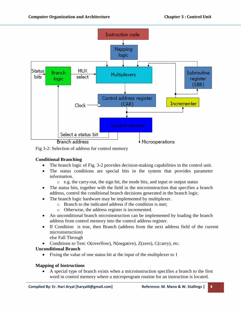
Fig. 3-2 shows a block diagram of a control memory and the associated hardware
needed for selecting the next microinstruction address.
The microinstruction in control memory contains
o a set of bits to initiate microoperations in computer registers
o Other bits to specify the method by which the next address is obtained
Sequencing Capabilities Required in Control Storage
Incrementing of the control address register
Unconditional and conditional branches
A mapping process from the bits of the machine instruction to an address for control
memory
A facility for subroutine call and return
Next
Address
generator
(Sequencer)
Control
Address
Register
Control
Memory
(ROM)
Control
Data
Register
Computer Organization and Architecture Chapter 3 : Control Unit
Compiled By: Er. Hari Aryal [[email protected]] Reference: M. Mano & W. Stallings | 4
Fig 3-2: Selection of address for control memory
Conditional Branching
The branch logic of Fig. 3-2 provides decision-making capabilities in the control unit.
The status conditions are special bits in the system that provides parameter
information.
o e.g. the carry-out, the sign bit, the mode bits, and input or output status
The status bits, together with the field in the microinstruction that specifies a branch
address, control the conditional branch decisions generated in the branch logic.
The branch logic hardware may be implemented by multiplexer.
o Branch to the indicated address if the condition is met;
o Otherwise, the address register is incremented.
An unconditional branch microinstruction can be implemented by loading the branch
address from control memory into the control address register.
If Condition is true, then Branch (address from the next address field of the current
microinstruction)
else Fall Through
Conditions to Test: O(overflow), N(negative), Z(zero), C(carry), etc.
Unconditional Branch
Fixing the value of one status bit at the input of the multiplexer to 1
Mapping of Instructions
A special type of branch exists when a microinstruction specifies a branch to the first
word in control memory where a microprogram routine for an instruction is located.

Computer Organization and Architecture Chapter 3 : Control Unit
Compiled By: Er. Hari Aryal [[email protected]] Reference: M. Mano & W. Stallings | 5
The status bits for this type of branch are the bits in the operation code part of the
instruction.
One simple mapping process that converts the 4-bit operation code to a 7-bit address
for control memory is shown in Fig. 3-3.
o Placing a 0 in the most significant bit of the address
o Transferring the four operation code bits
o Clearing the two least significant bits of the control address register
This provides for each computer instruction a microprogram routine with a capacity
of four microinstructions.
o If the routine needs more than four microinstructions, it can use addresses
1000000 through 1111111.
o If it uses fewer than four microinstructions, the unused memory locations
would be available for other routines.
One can extend this concept to a more general mapping rule by using a ROM or
programmable logic device (PLD) to specify the mapping function.
Fig 3-3: Mapping from instruction code to microinstruction address
Fig 3-3 (a): Direct mapping

Computer Organization and Architecture Chapter 3 : Control Unit
Compiled By: Er. Hari Aryal [[email protected]] Reference: M. Mano & W. Stallings | 6
Fig 3-3 (b): Mapping Function Implemented by ROM and PLD
Mapping from the OP-code of an instruction to the address of the Microinstruction which
is the starting microinstruction of its execution microprogram.
Subroutine
Subroutines are programs that are used by other routines to accomplish a particular
task.
Microinstructions can be saved by employing subroutines that use common sections
of microcode.
e.g. effective address computation
The subroutine register can then become the source for transferring the address for
the return to the main routine.
The best way to structure a register file that stores addresses for subroutines is to
organize the registers in a last-in, first-out (LIFO) stack.
3.3 Computer configuration
Once the configuration of a computer and its microprogrammed control unit is
established, the designer’s task is to generate the microcode for the control memory.
This microcode generation is called microprogramming.
The block diagram of the computer is shown in Below Fig.
Two memory units
o A main memory for storing instructions and data
o A control memory for storing the microprogram
Four registers are associated with the processor unit
o Program counter PC, address register AR, data register DR, accumulator
register AC
The control unit has a control address register CAR and a subroutine register SBR.
The control memory and its register are organized as a microprogrammed control
unit, as shown in Fig. 3-2.
The transfer of information among the registers in the processor is done through
multiplexers rather than a common bus.

Computer Organization and Architecture Chapter 3 : Control Unit
Compiled By: Er. Hari Aryal [[email protected]] Reference: M. Mano & W. Stallings | 7
Fig 3-4: Computer hardware configuration
3.4 Microinstruction Format
Computer Instruction Format
The computer instruction format is depicted in Fig. 3-5(a).
It consists of three fields:
o A 1-bit field for indirect addressing symbolized by I
o A 4-bit operation code (opcode)
o An 11-bit address field
Fig. 3-5(b) lists four of the 16 possible memory-reference instructions.
Fig. 3-5 (a): Instruction Format

Computer Organization and Architecture Chapter 3 : Control Unit
Compiled By: Er. Hari Aryal [[email protected]] Reference: M. Mano & W. Stallings | 8
Fig 3-5 (b): Four Computer Instructions
Microinstruction Format
The microinstruction format for the control memory is shown in Fig. 3-6.
The 20 bits of the microinstruction are divided into four functional parts.
o The three fields F1, F2, and F3 specify microoperations for the computer.
o The CD field selects status bit conditions.
o The BR field specifies the type of branch.
o The AD field contains a branch address.
Fig 3-6: Microinstruction code format
Microoperations
The three bits in each field are encoded to specify seven distinct microoperations
as listed in Table 3-1.
o No more than three microoperations can be chosen for a microinstruction,
one from each field.
o If fewer than three microoperations are used, one or more of the fields will
use the binary code 000 for no operation.
It is important to realize that two or more conflicting microoperations cannot be
specified simultaneously. e.g. 010 001 000
Each microoperation in Table 3-1 is defined with a register transfer statement and
is assigned a symbol for use in a symbolic microprogram.

Computer Organization and Architecture Chapter 3 : Control Unit
Compiled By: Er. Hari Aryal [[email protected]] Reference: M. Mano & W. Stallings | 9

Computer Organization and Architecture Chapter 3 : Control Unit
Compiled By: Er. Hari Aryal [[email protected]] Reference: M. Mano & W. Stallings | 10
Table 3-1 : Symbols and Binary code for Microinstruction Fields
Condition and Branch Field
The CD field consists of two bits which are encoded to specify four status bit
conditions as listed in Table 3-1.
The BR field consists of two bits. It is used, in conjunction with the address
field AD, to choose the address of the next microinstruction.
o The jump and call operations depend on the value of the CD field.
o The two operations are identical except that a call microinstruction stores
the return address in the subroutine register SBR.
o Note that the last two conditions in the BR field are independent of the
values in the CD and AD fields.
3.5 Symbolic Microinstructions
The symbols defined in Table 3-1 cab be used to specify microinstructions in
symbolic form.
Symbols are used in microinstructions as in assembly language
The simplest and most straightforward way to formulate an assembly
language for a microprogram is to define symbols for each field of the
microinstruction and to give users the capability for defining their own
symbolic addresses.
A symbolic microprogram can be translated into its binary equivalent by a
microprogram assembler.
Computer Organization and Architecture Chapter 3 : Control Unit
Compiled By: Er. Hari Aryal [[email protected]] Reference: M. Mano & W. Stallings | 11
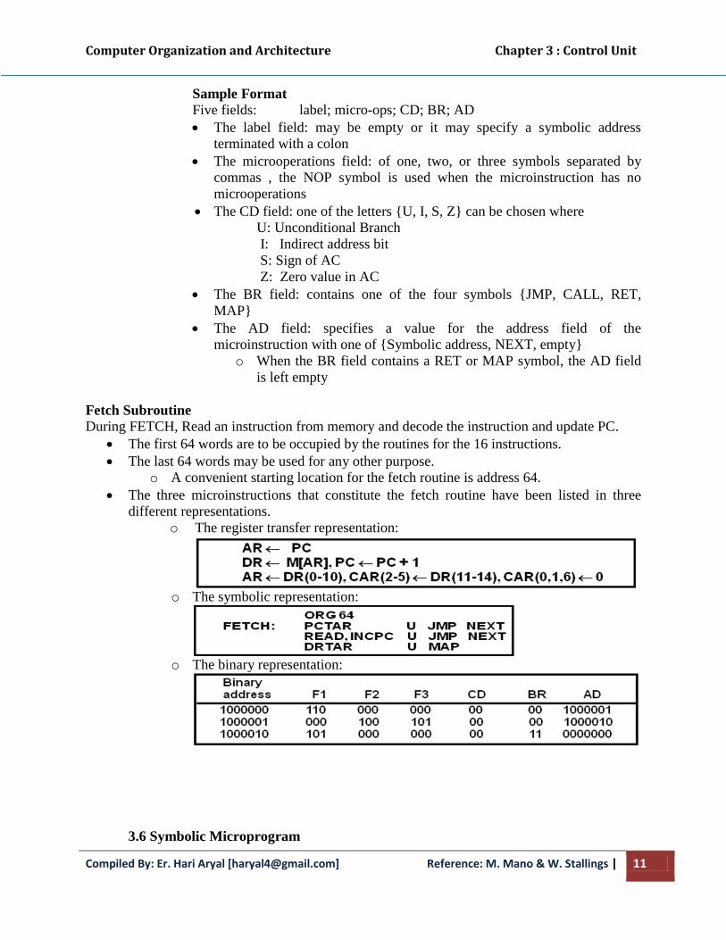
Sample Format
Five fields: label; micro-ops; CD; BR; AD
The label field: may be empty or it may specify a symbolic address
terminated with a colon
The microoperations field: of one, two, or three symbols separated by
commas , the NOP symbol is used when the microinstruction has no
microoperations
The CD field: one of the letters {U, I, S, Z} can be chosen where
U: Unconditional Branch
I: Indirect address bit
S: Sign of AC
Z: Zero value in AC
The BR field: contains one of the four symbols {JMP, CALL, RET,
MAP}
The AD field: specifies a value for the address field of the
microinstruction with one of {Symbolic address, NEXT, empty}
o When the BR field contains a RET or MAP symbol, the AD field
is left empty
Fetch Subroutine
During FETCH, Read an instruction from memory and decode the instruction and update PC.
The first 64 words are to be occupied by the routines for the 16 instructions.
The last 64 words may be used for any other purpose.
o A convenient starting location for the fetch routine is address 64.
The three microinstructions that constitute the fetch routine have been listed in three
different representations.
o The register transfer representation:
o The symbolic representation:
o The binary representation:
3.6 Symbolic Microprogram

Computer Organization and Architecture Chapter 3 : Control Unit
Compiled By: Er. Hari Aryal [[email protected]] Reference: M. Mano & W. Stallings | 12
Control Storage: 128 20-bit words
The first 64 words: Routines for the 16 machine instructions 0, 4, 8, …, 60 gives four
words in control memory for each routine.
The last 64 words: Used for other purpose (e.g., fetch routine and other subroutines)
The execution of the third (MAP) microinstruction in the fetch routine results in a
branch to address 0xxxx00, were xxxx are the four bits of the operation code. e.g.
ADD is 0000
In each routine we must provide microinstructions for evaluating the effective address
and for executing the instruction.
The indirect address mode is associated with all memory-reference instructions.
A saving in the number of control memory words may be achieved if the
microinstructions for the indirect address are stored as a subroutine.
This subroutine, INDRCT, is located right after the fetch routine, as shown in Table
3-2.
Mapping: OP-code XXXX into 0XXXX00, the first address for the 16 routines are
0(0 0000 00), 4(0 0001 00), 8, 12, 16, 20, ..., 60
To see how the transfer and return from the indirect subroutine occurs:
o MAP microinstruction caused a branch to address 0
o The first microinstruction in the ADD routine calls subroutine INDRCT when
I=1
o The return address is stored in the subroutine register SBR.
o The INDRCT subroutine has two microinstructions:
INDRCT: READ U JMP NEXT
DRTAR U RET
o Therefore, the memory has to be accessed to get the effective address, which
is then transferred to AR.
o The execution of the ADD instruction is carried out by the microinstructions
at addresses 1 and 2
o The first microinstruction reads the operand from memory into DR.
o The second microinstruction performs an add microoperation with the content
of DR and AC and then jumps back to the beginning of the fetch routine.

Computer Organization and Architecture Chapter 3 : Control Unit
Compiled By: Er. Hari Aryal [[email protected]] Reference: M. Mano & W. Stallings | 13
Table 3-2: Symbolic Microprogram for Control Memory (Partial)
Binary Microprogram
The symbolic microprogram must be translated to binary either by means of an
assembler program or by the user if the microprogram is simple.
The equivalent binary form of the microprogram is listed in Table 7-3.
Even though address 3 is not used, some binary value, e.g. all 0’s, must be
specified for each word in control memory.
However, if some unforeseen error occurs, or if a noise signal sets CAR to the
value of 3, it will be wise to jump to address 64.

Computer Organization and Architecture Chapter 3 : Control Unit
Compiled By: Er. Hari Aryal [[email protected]] Reference: M. Mano & W. Stallings | 14
Table 3-3: Binary Microprogram for control memory (Partial)
Control Memory
When a ROM is used for the control memory,the microprogram binary list
provides the truth table for fabricating the unit.
o To modify the instruction set of the computer, it is necessary to generate a
new microprogram and mask a new ROM.
The advantage of employing a RAM for the control memory is that the
microprogram can be altered simply by writing a new pattern of 1’s and 0’s
without resorting to hardware procedure.
However, most microprogram systems use a ROM for the control memory
because it is cheaper and faster than a RAM.
3.7 Control Unit Operation
Microoperations
A computer executes a program consisting instructions. Each instruction is
made up of shorter sub-cycles as fetch, indirect, execute cycle, interrupt.
Performance of each cycle has a number of shorter operations called micro-
operations.
Called so because each step is very simple and does very little.
Thus micro-operations are functional atomic operation of CPU.

Computer Organization and Architecture Chapter 3 : Control Unit
Compiled By: Er. Hari Aryal [[email protected]] Reference: M. Mano & W. Stallings | 15
Hence events of any instruction cycle can be described as a sequence of
micro-operations
Fig 3-7: Constituent Elements of Program Execution
Steps leading to characterization of CU
Define basic elements of processor
Describe micro-operations processor performs
Determine functions control unit must perform
Types of Micro-operation
Transfer data between registers
Transfer data from register to external interface
Transfer data from external interface to register
Perform arithmetic/logical ops with register for i/p, o/p
Functions of Control Unit
Sequencing
Causing the CPU to step through a series of micro-operations
Execution
Causing the performance of each micro-op

Computer Organization and Architecture Chapter 3 : Control Unit
Compiled By: Er. Hari Aryal [[email protected]] Reference: M. Mano & W. Stallings | 16
These are done using Control Signals
Fig 3-8: Control Unit Layout
Inputs to Control Unit
Clock
o CU causes one micro-instruction (or set of parallel micro-instructions) per
clock cycle
Instruction register
o Op-code for current instruction determines which micro-instructions are
performed
Flags
o State of CPU
o Results of previous operations
From control bus
o Interrupts
o Acknowledgements
CU Outputs (Control Signals)
Within CPU(two types)
o Cause data movement
o Activate specific ALU functions
Via control bus(two types)
o To memory
o To I/O modules
Types of Control Signals
o Those that activate an ALU
o Those that activate a data path
o Those that are signal on external system bus or other external interface.
All these are applied as binary i/p to individual logic gates

Computer Organization and Architecture Chapter 3 : Control Unit
Compiled By: Er. Hari Aryal [[email protected]] Reference: M. Mano & W. Stallings | 17
Hardwired Implementation
In this implementation, CU is essentially a combinational circuit. Its i/p signals
are transformed into set of o/p logic signal which are control signals.
Control unit inputs
Flags and control bus
o Each bit means something
Instruction register
o Op-code causes different control signals for each different instruction
o Unique logic for each op-code
o Decoder takes encoded input and produces single output
o Each decoder i/p will activate a single unique o/p
Clock
o Repetitive sequence of pulses
o Useful for measuring duration of micro-ops
o Must be long enough to allow signal propagation along data paths and
through processor circuitry
o Different control signals at different times within instruction cycle
o Need a counter as i/p to control unit with different control signals being
used for t1, t2 etc.
o At end of instruction cycle, counter is re-initialised
Fig 3-9: Control Unit With Decoded Input
Computer Organization and Architecture Chapter 3 : Control Unit
Compiled By: Er. Hari Aryal [[email protected]] Reference: M. Mano & W. Stallings | 18
Implementation
For each control signal, a Boolean expression of that signal as a function of the
inputs is derived
With that the combinatorial circuit is realized as control unit.
Problems With Hard Wired Designs
Complex sequencing & micro-operation logic
Difficult to design and test
Inflexible design
Difficult to add new instructions
Micro-programmed Implementation
An alternative to hardwired CU
Common in contemporary CISC processors
Use sequences of instructions to perform control operations performed by micro
operations called micro-programming or firmware
Fig 3-10: Microprogrammed Control Unit

Computer Organization and Architecture Chapter 3 : Control Unit
Compiled By: Er. Hari Aryal [[email protected]] Reference: M. Mano & W. Stallings | 19
Set of microinsrurctions are stored in control memory
Control address register contains the address of the next microinstruction to be read
As it is read, it is transferred to control buffer register.
For horizontal micro instructions, reading a microinstruction is same as executing it.
Sequencing unit loads the control address register and issues a read command
CU functions as follows to execute an instruction:
Sequencing logic issues read command to control memory
Word whose address is in control address register is read into control buffer register.
Content of control buffer register generates control signals and next address instruction
for the sequencing logic unit.
Sequencing logic unit loads new address into control address register depending upon the
value of ALU flags, control buffer register.
One of following decision is made:
o add 1 to control address register
o load address from address field of control buffer register
o load the control address register based on opcode in IR
Upper decoder translates the opcode of IR into control memory address.
Lower decoder used for veritcal micro instructions.
Micro-instruction Types
Each micro-instruction specifies single or few micro-operations to be performed -
vertical micro-programming
Each micro-instruction specifies many different micro-operations to be performed in
parallel - horizontal micro-programming
Horizontal Micro-programming
Wide memory word
High degree of parallel operations possible
Little encoding of control information
Vertical Micro-programming
Width is narrow
n control signals encoded into log2 n bits
Limited ability to express parallelism
Considerable encoding of control information requires external memory word
decoder to identify the exact control line being manipulated

Computer Organization and Architecture Chapter 3 : Control Unit
Compiled By: Er. Hari Aryal [[email protected]] Reference: M. Mano & W. Stallings | 20
3.8 Design of Control Unit
The bits of the microinstruction are usually divided into fields, with each field
defining a distinct, separate function.
The various fields encountered in instruction formats provide:
o Control bits to initiate microoperations in the system
o Special bits to specify the way that the next address is to be evaluated
o An address field for branching
The number of control bits that initiate microoperations can be reduced by grouping
mutually exclusive variables into fields by encoding the k bits in each field to provide
2k microoperations.
Each field requires a decoder to produce the corresponding control signals.
o Reduces the size of the microinstruction bits
o Requires additional hardware external to the control memory
o Increases the delay time of the control signals
Fig. 3-11 shows the three decoders and some of the connections that must be made
from their outputs.
Outputs 5 or 6 of decoder F1 are connected to the load input of AR so that when
either one of these outputs is active; information from the multiplexers is transferred
to AR.
The transfer into AR occurs with a clock pulse transition only when output 5 (from
DR (0-10) to AR i.e. DRTAR) or output 6 (from PC to AR i.e. PCTAR) of the
decoder are active.
The arithmetic logic shift unit can be designed instead of using gates to generate the
control signals; it comes from the outputs of the decoders.

Computer Organization and Architecture Chapter 3 : Control Unit
Compiled By: Er. Hari Aryal [[email protected]] Reference: M. Mano & W. Stallings | 21
Fig 3-11: Decoding of Microoperation fields
Microprogram Sequencer
The basic components of a microprogrammed control unit are the control memory and
the circuits that select the next address.
The address selection part is called a microprogram sequencer.
A microprogram sequencer can be constructed with digital functions to suit a particular
application.
To guarantee a wide range of acceptability, an integrated circuit sequencer must provide
an internal organization that can be adapted to a wide range of application.
The purpose of a microprogram sequencer is to present an address to the control memory
so that a microinstruction may be read and executed.
The block diagram of the microprogram sequencer is shown in Fig. 3-12.
o The control memory is included to show the interaction between the sequencer
and the attached to it.
o There are two multiplexers in the circuit; first multiplexer selects an address from
one of the four sources and routes to CAR, second multiplexer tests the value of
the selected status bit and result is applied to an input logic circuit.
o The output from CAR provides the address for control memory, contents of CAR
incremented and applied to one of the multiplexers input and to the SBR.

Computer Organization and Architecture Chapter 3 : Control Unit
Compiled By: Er. Hari Aryal [[email protected]] Reference: M. Mano & W. Stallings | 22
o Although the diagram shows a single subroutine register, a typical sequencer will
have a register stack about four to eight levels deep. In this way, a push, pop
operation and stack pointer operates for subroutine call and return instructions.
o The CD (Condition) field of the microinstruction selects one of the status bits in
the second multiplexer.
o The Test variable (either 1 or 0) i.e. T value together with the two bits from the
BR (Branch) field go to an input logic circuit.
o The input logic circuit determines the type of the operation.
Fig 3-12: Microprom Sequencer for a Control Memory
Design of Input Logic
The input logic in a particular sequencer will determine the type of operations that are
available in the unit.
Typical sequencer operations are: increment, branch or jump, call and return from
subroutine, load an external address, push or pop the stack, and other address
sequencing operations.
Computer Organization and Architecture Chapter 3 : Control Unit
Compiled By: Er. Hari Aryal [[email protected]] Reference: M. Mano & W. Stallings | 23
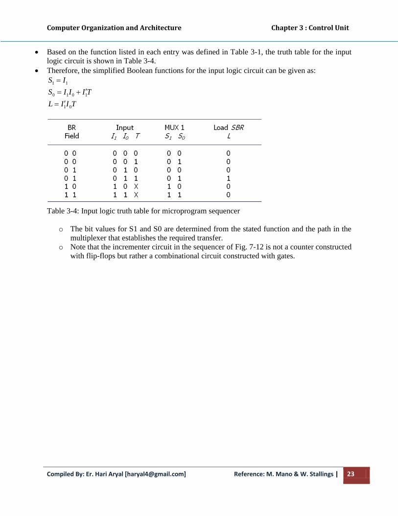
Based on the function listed in each entry was defined in Table 3-1, the truth table for the input
logic circuit is shown in Table 3-4.
Therefore, the simplified Boolean functions for the input logic circuit can be given as:
TIIL
TIIIS
IS
01
1010
11
Table 3-4: Input logic truth table for microprogram sequencer
o The bit values for S1 and S0 are determined from the stated function and the path in the
multiplexer that establishes the required transfer.
o Note that the incrementer circuit in the sequencer of Fig. 7-12 is not a counter constructed
with flip-flops but rather a combinational circuit constructed with gates.