Chapter 33.2 Boolean Algebra (4 of 17) •A Boolean function has: –at least one Boolean variable,...
37
2/21/2019 1 Chapter 3 Boolean Algebra and Digital Logic Objectives • Understand the relationship between Boolean logic and digital computer circuits. • Learn how to design simple logic circuits. • Understand how digital circuits work together to form complex computer systems. 3.1 Introduction (1 of 2) • In the latter part of the nineteenth century, George Boole incensed philosophers and mathematicians alike when he suggested that logical thought could be represented through mathematical equations. – How dare anyone suggest that human thought could be encapsulated and manipulated like an algebraic formula? • Computers, as we know them today, are implementations of Boole’s Laws of Thought. – John Atanasoff and Claude Shannon were among the first to see this connection.
Transcript of Chapter 33.2 Boolean Algebra (4 of 17) •A Boolean function has: –at least one Boolean variable,...

2/21/2019
1
Chapter 3
Boolean Algebra and Digital Logic
Objectives
• Understand the relationship between Boolean
logic and digital computer circuits.
• Learn how to design simple logic circuits.
• Understand how digital circuits work together
to form complex computer systems.
3.1 Introduction (1 of 2)
• In the latter part of the nineteenth century, George Boole incensed philosophers and mathematicians alike when he suggested that logical thought could be represented through mathematical equations.– How dare anyone suggest that human thought could
be encapsulated and manipulated like an algebraic formula?
• Computers, as we know them today, are implementations of Boole’s Laws of Thought.– John Atanasoff and Claude Shannon were among the
first to see this connection.
2/21/2019
2
3.1 Introduction (2 of 2)
• In the middle of the twentieth century, computers were commonly known as “thinking machines” and “electronic brains.”
– Many people were fearful of them.
• Nowadays, we rarely ponder the relationship between electronic digital computers and human logic. Computers are accepted as part of our lives.
– Many people, however, are still fearful of them.
• In this chapter, you will learn the simplicity that constitutes the essence of the machine.
3.2 Boolean Algebra (1 of 17)
• Boolean algebra is a mathematical system for the manipulation of variables that can have one of two values.– In formal logic, these values are “true” and “false.”
– In digital systems, these values are “on” and “off,” 1 and 0, or “high” and “low.”
• Boolean expressions are created by performing operations on Boolean variables.– Common Boolean operators include AND, OR, and
NOT.
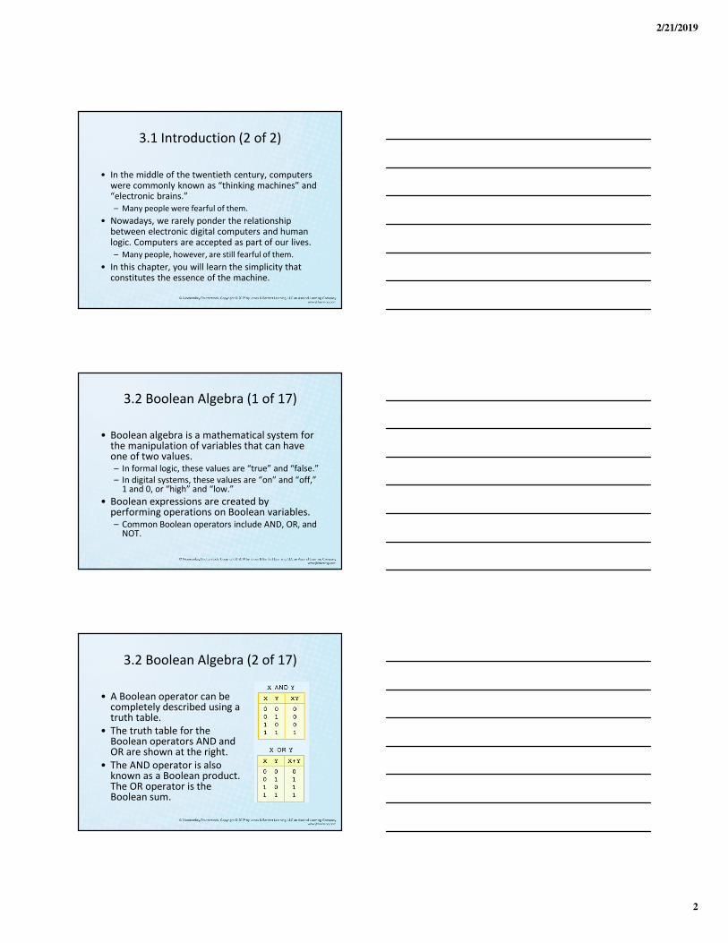
3.2 Boolean Algebra (2 of 17)
• A Boolean operator can be completely described using a truth table.
• The truth table for the Boolean operators AND and OR are shown at the right.
• The AND operator is also known as a Boolean product. The OR operator is the Boolean sum.

2/21/2019
3
3.2 Boolean Algebra (3 of 17)
• The truth table for the
Boolean NOT operator is
shown at the right.
• The NOT operation is most
often designated by a prime
mark (X’). It is sometimes
indicated by an overbar (X�)
or an “elbow” (¬¬¬¬X).
3.2 Boolean Algebra (4 of 17)
• A Boolean function has:
– at least one Boolean variable,
– at least one Boolean operator, and
– at least one input from the set {0,1}.
• It produces an output that is also a
member of the set {0,1}.
Now you know why the binary numbering system is so
handy in digital systems.
3.2 Boolean Algebra (5 of 17)
• The truth table for the Boolean function:
is shown at the right.
• To make evaluation of the Boolean function easier, the truth table contains extra (shaded) columns to hold evaluations of subparts of the function.

2/21/2019
4
3.2 Boolean Algebra (6 of 17)
• As with common arithmetic, Boolean operations have rules of precedence.
• The NOT operator has highest priority, followed by AND and then OR.
• This is how we chose the (shaded) function subparts in our table.
3.2 Boolean Algebra (7 of 17)
• Digital computers contain circuits that implement Boolean functions.
• The simpler that we can make a Boolean function, the smaller the circuit that will result.
– Simpler circuits are cheaper to build, consume less power, and run faster than complex circuits.
• With this in mind, we always want to reduce our Boolean functions to their simplest form.
• There are a number of Boolean identities that help us to do this.
3.2 Boolean Algebra (8 of 17)
• Most Boolean identities have an AND
(product) form as well as an OR (sum) form.
We give our identities using both forms.
Our first group is rather intuitive:

2/21/2019
5
3.2 Boolean Algebra (9 of 17)
• Our second group of Boolean identities
should be familiar to you from your study
of algebra:
3.2 Boolean Algebra (10 of 17)
• Our last group of Boolean identities are
perhaps the most useful.
• If you have studied set theory or formal
logic, these laws are also familiar to you.
3.2 Boolean Algebra (11 of 17)
• We can use Boolean identities to simplify:
F(x,y,z) = xy + x′z + yz

2/21/2019
6
3.2 Boolean Algebra (12 of 17)
• Sometimes it is more economical to build a circuit using the complement of a function (and complementing its result) than it is to implement the function directly.
• DeMorgan’s law provides an easy way of finding the complement of a Boolean function.
• Recall DeMorgan’s law states:(xy)’ = x’+ y’ and (x + y)’= x’y’
3.2 Boolean Algebra (13 of 17)
• DeMorgan’s law can be extended to any number of
variables.
• Replace each variable by its complement and
change all ANDs to ORs and all ORs to ANDs.
• Thus, we find the complement of:
is:
3.2 Boolean Algebra (14 of 17)
• Through our exercises in simplifying Boolean expressions, we see that there are numerous ways of stating the same Boolean expression.– These “synonymous” forms are logically
equivalent.
– Logically equivalent expressions have identical truth tables.
• In order to eliminate as much confusion as possible, designers express Boolean functions in standardized or canonical form.

2/21/2019
7
3.2 Boolean Algebra (15 of 17)
• There are two canonical forms for Boolean expressions: sum-of-products and product-of-sums.
– Recall the Boolean product is the AND operation and the Boolean sum is the OR operation.
• In the sum-of-products form, ANDed variables are ORed together.
– For example:
• In the product-of-sums form, ORed variables are ANDed together.
– For example:
3.2 Boolean Algebra (16 of 17)
• It is easy to convert a function to sum-of-products form using its truth table.
• We are interested in the values of the variables that make the function true (= 1).
• Using the truth table, we list the values of the variables that result in a true function value.
• Each group of variables is then ORed together.
3.2 Boolean Algebra (17 of 17)
• The sum-of-products form for
our function is:
We note that this function is not in simplest terms. Our aim is only to
rewrite our function in canonical sum-of-products form.
2/21/2019
8
3.3 Logic Gates (1 of 6)
• We have looked at Boolean functions in abstract terms.
• In this section, we see that Boolean functions are implemented in digital computer circuits called gates.
• A gate is an electronic device that produces a result based on two or more input values.– In reality, gates consist of one to six transistors, but
digital designers think of them as a single unit.
– Integrated circuits contain collections of gates suited to a particular purpose.
3.3 Logic Gates (2 of 6)
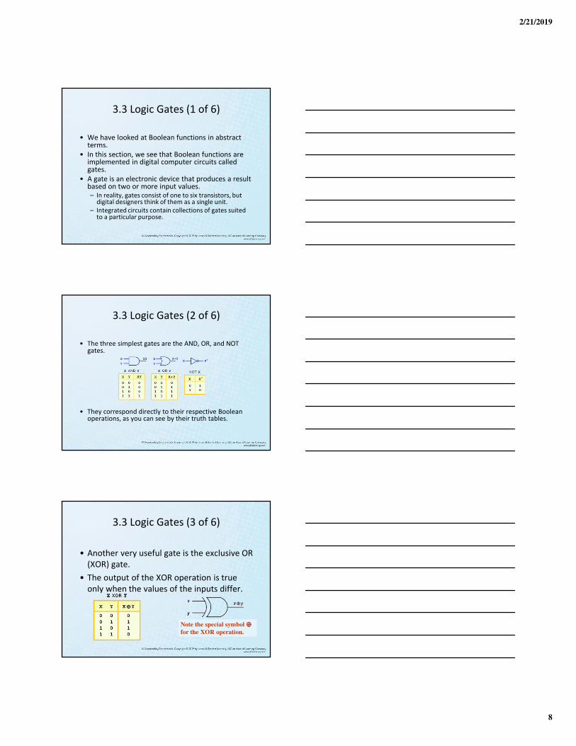
• The three simplest gates are the AND, OR, and NOT gates.
• They correspond directly to their respective Boolean operations, as you can see by their truth tables.
3.3 Logic Gates (3 of 6)
• Another very useful gate is the exclusive OR
(XOR) gate.
• The output of the XOR operation is true
only when the values of the inputs differ.
Note the special symbol ⊕⊕⊕⊕
for the XOR operation.

2/21/2019
9
3.3 Logic Gates (4 of 6)
• NAND and NOR are two very important gates. Their symbols and truth tables are shown at the right.
3.3 Logic Gates (5 of 6)
• NAND and NOR are known as universal gates because they are inexpensive to manufacture and any Boolean function can be constructed using only NAND or only NOR gates.
3.3 Logic Gates (6 of 6)
• Gates can have multiple inputs and more
than one output.
– A second output can be provided for the
complement of the operation.
– We’ll see more of this later.
2/21/2019
10
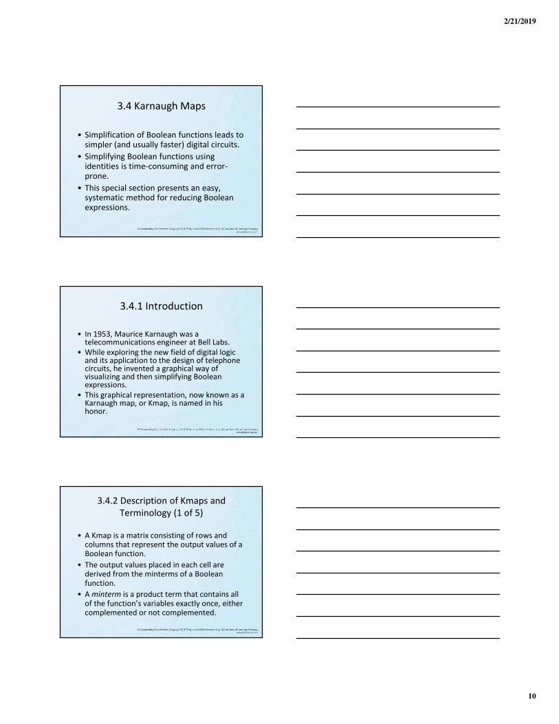
3.4 Karnaugh Maps
• Simplification of Boolean functions leads to simpler (and usually faster) digital circuits.
• Simplifying Boolean functions using identities is time-consuming and error-prone.
• This special section presents an easy, systematic method for reducing Boolean expressions.
3.4.1 Introduction
• In 1953, Maurice Karnaugh was a telecommunications engineer at Bell Labs.
• While exploring the new field of digital logic and its application to the design of telephone circuits, he invented a graphical way of visualizing and then simplifying Boolean expressions.
• This graphical representation, now known as a Karnaugh map, or Kmap, is named in his honor.
3.4.2 Description of Kmaps and
Terminology (1 of 5)
• A Kmap is a matrix consisting of rows and columns that represent the output values of a Boolean function.
• The output values placed in each cell are derived from the minterms of a Boolean function.
• A minterm is a product term that contains all of the function’s variables exactly once, either complemented or not complemented.

2/21/2019
11
• For example, the minterms for a function having the
inputs x and y are x’y, x’y, xy’, and xy.
• Consider the Boolean function, F(x,y)= xy + xy’
• Its minterms are:
3.4.2 Description of Kmaps and
Terminology (2 of 5)
3.4.2 Description of Kmaps and
Terminology (3 of 5)
• Similarly, a function having three inputs,
has the minterms that are shown in this
diagram.
3.4.2 Description of Kmaps and
Terminology (4 of 5)
• A Kmap has a cell for each minterm.
• This means that it has a cell for each line for the truth table of a function.
• The truth table for the function F(x,y) = xy is shown at the right along with its corresponding Kmap.
2/21/2019
12
3.4.2 Description of Kmaps and
Terminology (5 of 5)
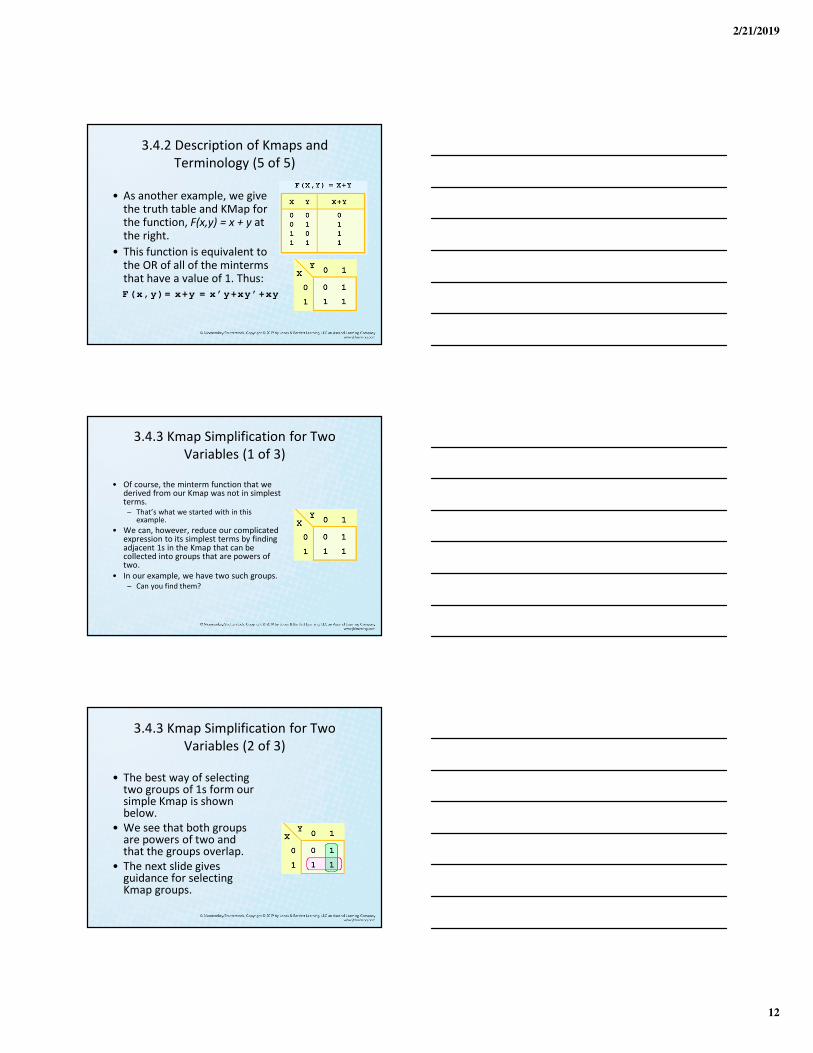
• As another example, we give the truth table and KMap for the function, F(x,y) = x + y at the right.
• This function is equivalent to the OR of all of the minterms that have a value of 1. Thus:
F(x,y)= x+y = x’y+xy’+xy
3.4.3 Kmap Simplification for Two
Variables (1 of 3)
• Of course, the minterm function that we derived from our Kmap was not in simplest terms.
– That’s what we started with in this example.
• We can, however, reduce our complicated expression to its simplest terms by finding adjacent 1s in the Kmap that can be collected into groups that are powers of two.
• In our example, we have two such groups.
– Can you find them?
3.4.3 Kmap Simplification for Two
Variables (2 of 3)
• The best way of selecting two groups of 1s form our simple Kmap is shown below.
• We see that both groups are powers of two and that the groups overlap.
• The next slide gives guidance for selecting Kmap groups.
2/21/2019
13
3.4.3 Kmap Simplification for Two
Variables (3 of 3)
• The rules of Kmap simplification are:
– Groupings can contain only 1s; no 0s.
– Groups can be formed only at right angles; diagonal groups are not allowed.
– The number of 1s in a group must be a power of 2 – even if it contains a single 1.
– The groups must be made as large as possible.
– Groups can overlap and wrap around the sides of the Kmap.
3.4.4 Kmap Simplification for Three
Variables (1 of 7)
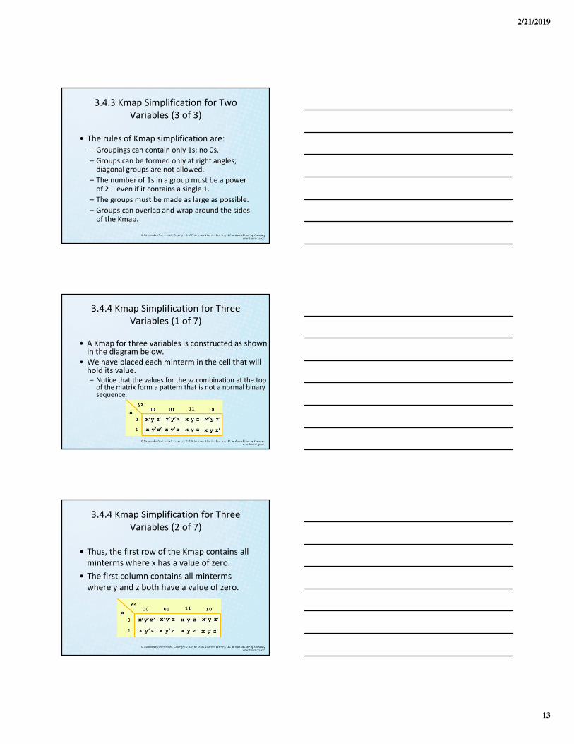
• A Kmap for three variables is constructed as shown in the diagram below.
• We have placed each minterm in the cell that will hold its value.– Notice that the values for the yz combination at the top
of the matrix form a pattern that is not a normal binary sequence.
3.4.4 Kmap Simplification for Three
Variables (2 of 7)
• Thus, the first row of the Kmap contains all
minterms where x has a value of zero.
• The first column contains all minterms
where y and z both have a value of zero.
2/21/2019
14
3.4.4 Kmap Simplification for Three
Variables (3 of 7)
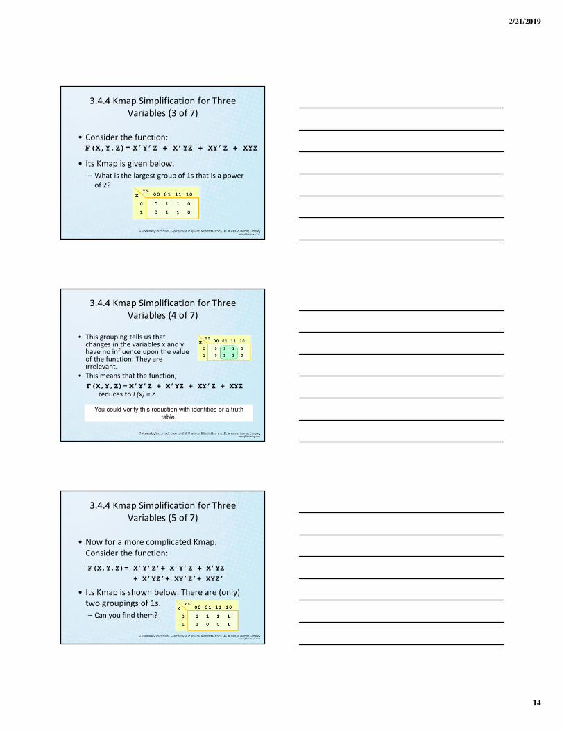
• Consider the function:
• Its Kmap is given below.
– What is the largest group of 1s that is a power
of 2?
F(X,Y,Z)= X’Y’Z + X’YZ + XY’Z + XYZ
3.4.4 Kmap Simplification for Three
Variables (4 of 7)
• This grouping tells us that changes in the variables x and y have no influence upon the value of the function: They are irrelevant.
• This means that the function,
reduces to F(x) = z.
You could verify this reduction with identities or a truth
table.
F(X,Y,Z)= X’Y’Z + X’YZ + XY’Z + XYZ
3.4.4 Kmap Simplification for Three
Variables (5 of 7)
• Now for a more complicated Kmap.
Consider the function:
• Its Kmap is shown below. There are (only)
two groupings of 1s.
– Can you find them?
F(X,Y,Z)= X’Y’Z’+ X’Y’Z + X’YZ
+ X’YZ’+ XY’Z’+ XYZ’

2/21/2019
15
3.4.4 Kmap Simplification for Three
Variables (6 of 7)
• In this Kmap, we see an example of a group that wraps around the sides of a Kmap.
• This group tells us that the values of x and yare not relevant to the term of the function that is encompassed by the group.
– What does this tell us about this term of the function?
What about the
green group in
the top row?
• The green group in the top row tells us that only the
value of x is significant in that group.
• We see that it is complemented in that row, so the
other term of the reduced function is X’
• Our reduced function is F(X,Y,Z)= X’+ Z’
Recall that we had
six minterms in our
original function!
3.4.4 Kmap Simplification for Three
Variables (7 of 7)
3.4.5 Kmap Simplification for Four
Variables (1 of 4)
• Our model can be extended to
accommodate the 16 minterms that are
produced by a four-input function.
• This is the format for a 16-minterm Kmap:

2/21/2019
16
3.4.5 Kmap Simplification for Four
Variables (2 of 4)
• We have populated the Kmap shown below
with the nonzero minterms from the function:
– Can you identify (only) three groups in this Kmap?
Recall that
groups can
overlap.
F(W,X,Y,Z)= W’X’Y’Z’+ W’X’Y’Z + W’X’YZ’
+ W’XYZ’+ WX’Y’Z’+ WX’Y’Z + WX’YZ’
3.4.5 Kmap Simplification for Four
Variables (3 of 4)
• Our three groups consist of:
– A purple group entirely within the Kmap at the right.
– A pink group that wraps the top and bottom.
– A green group that spans the corners.
• Thus we have three terms in our final function:
F(W,X,Y,Z)= W’Y’+ X’Z’
+ W’YZ’
3.4.5 Kmap Simplification for Four
Variables (4 of 4)
• It is possible to have a choice as to how to pick groups within a Kmap, while keeping the groups as large as possible.
• The (different) functions that result from the groupings below are logically equivalent.

2/21/2019
17
3.4.6 Don’t Care Conditions (1 of 5)
• Real circuits don’t always need to have an output defined for every possible input.– For example, some calculator displays consist of 7-
segment LEDs. These LEDs can display 27 – 1 patterns, but only ten of them are useful.
• If a circuit is designed so that a particular set of inputs can never happen, we call this set of inputs a don’t care condition.
• They are very helpful to us in Kmap circuit simplification.
3.4.6 Don’t Care Conditions (2 of 5)
• In a Kmap, a don’t care condition is identified by an X in the cell of the minterm(s) for the don’t care inputs, as shown here.
• In performing the simplification, we are free to include or ignore the X’s when creating our groups.
3.4.6 Don’t Care Conditions (3 of 5)
• In one grouping in the Kmap below, we
have the function:
F(W,X,Y,Z)= W’Y’+ YZ
2/21/2019
18
3.4.6 Don’t Care Conditions (4 of 5)
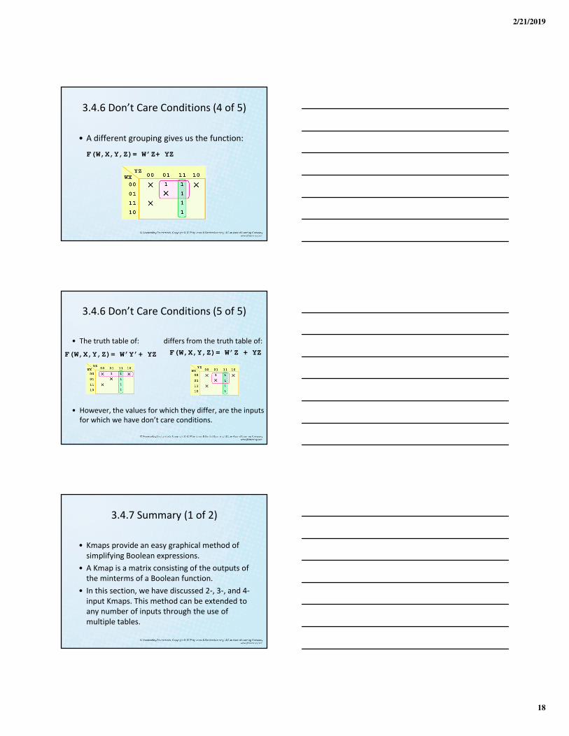
• A different grouping gives us the function:
F(W,X,Y,Z)= W’Z+ YZ
3.4.6 Don’t Care Conditions (5 of 5)
• The truth table of: differs from the truth table of:
• However, the values for which they differ, are the inputs
for which we have don’t care conditions.
F(W,X,Y,Z)= W’Y’+ YZ F(W,X,Y,Z)= W’Z + YZ
3.4.7 Summary (1 of 2)
• Kmaps provide an easy graphical method of
simplifying Boolean expressions.
• A Kmap is a matrix consisting of the outputs of
the minterms of a Boolean function.
• In this section, we have discussed 2-, 3-, and 4-
input Kmaps. This method can be extended to
any number of inputs through the use of
multiple tables.

2/21/2019
19
3.4.7 Summary (2 of 2)
• Recapping the rules of Kmap simplification:– Groupings can contain only 1s; no 0s.
– Groups can be formed only at right angles; diagonal groups are not allowed.
– The number of 1s in a group must be a power of 2 – even if it contains a single 1.
– The groups must be made as large as possible.
– Groups can overlap and wrap around the sides of the Kmap.
– Use don’t care conditions when you can.
3.5 Digital Components (1 of 8)
• The main thing to remember is that combinations of gates implement Boolean functions.
• The circuit below implements the Boolean function F(x,y,z) = x + y’z:
We simplify our Boolean expressions so
that we can create simpler circuits.
3.5 Digital Components (2 of 8)
• Standard digital components are combined
into single integrated circuit packages.
• Boolean logic can be used to implement
the desired functions.

2/21/2019
20
3.5 Digital Components (3 of 8)
• The Boolean circuit:
• Can be rendered using only NAND gates as:
3.5 Digital Components (4 of 8)
• So we can wire the pre-packaged circuit to
implement our function:
3.5 Digital Components (5 of 8)
• Boolean logic is used to solve practical
problems.
• Expressed in terms of Boolean logic
practical problems can be expressed by
truth tables.
• Truth tables can be readily rendered into
Boolean logic circuits.

2/21/2019
21
3.5 Digital Components (6 of 8)
• Suppose we are to design a logic circuit to determine the best time to plant a garden.
• We consider three factors (inputs): – (1) time, where 0 represents day and 1 represents
evening;
– (2) moon phase, where 0 represents not full and 1 represents full; and
– (3) temperature, where 0 represents 45°F and below, and 1 represents over 45°F.
• We determine that the best time to plant a garden is during the evening with a full moon.
3.5 Digital Components (7 of 8)
• This results in the following truth table:
3.5 Digital Components (8 of 8)
• From the truth table, we derive the circuit:

2/21/2019
22
3.6 Combinational Circuits (1 of 12)
• We have designed a circuit that implements the Boolean function:
• This circuit is an example of a combinational logic circuit.
• Combinational logic circuits produce a specified output (almost) at the instant when input values are applied.– In a later section, we will explore circuits where this is
not the case.
3.6 Combinational Circuits (2 of 12)
• Combinational logic circuits give us many useful devices.
• One of the simplest is the half adder, which finds the sum of two bits.
• We can gain some insight as to the construction of a half adder by looking at its truth table, shown at the right.
3.6 Combinational Circuits (3 of 12)
• As we see, the sum can be found using the
XOR operation and the carry using the AND
operation.

2/21/2019
23
3.6 Combinational Circuits (4 of 12)
• We can change our half adder into to a full adder by including gates for processing the carry bit.
• The truth table for a full adder is shown at the right.
3.6 Combinational Circuits (5 of 12)
• How can we change the half adder shown
below to make it a full adder?
3.6 Combinational Circuits (6 of 12)
• Here’s our completed full adder.
2/21/2019
24
3.6 Combinational Circuits (7 of 12)
• Just as we combined half adders to make a full adder, full adders can connected in series.
• The carry bit “ripples” from one adder to the next; hence, this configuration is called a ripple-carry adder.
Today’s systems employ more efficient adders.
3.6 Combinational Circuits (8 of 12)
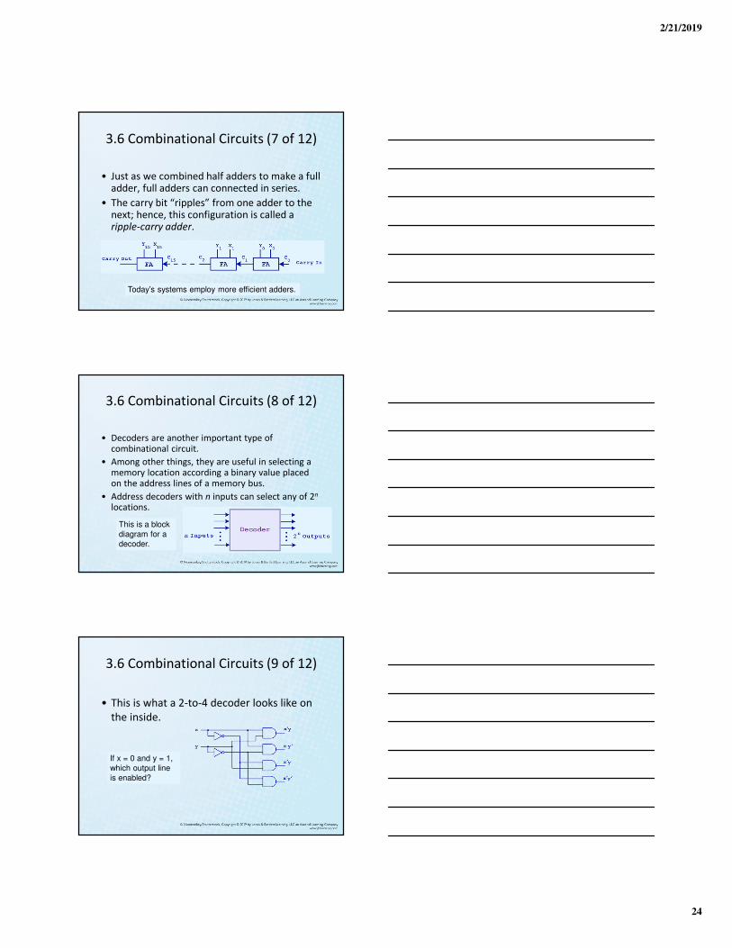
• Decoders are another important type of combinational circuit.
• Among other things, they are useful in selecting a memory location according a binary value placed on the address lines of a memory bus.
• Address decoders with n inputs can select any of 2n
locations.
This is a block
diagram for a
decoder.
3.6 Combinational Circuits (9 of 12)
• This is what a 2-to-4 decoder looks like on
the inside.
If x = 0 and y = 1,
which output line
is enabled?
2/21/2019
25
3.6 Combinational Circuits (10 of 12)
• A multiplexer does just the opposite of a decoder.
• It selects a single output from several inputs.
• The particular input chosen for output is determined by the value of the multiplexer’s control lines.
• To be able to select among ninputs, log2n control lines are needed.
• This is a block diagram for a multiplexer.
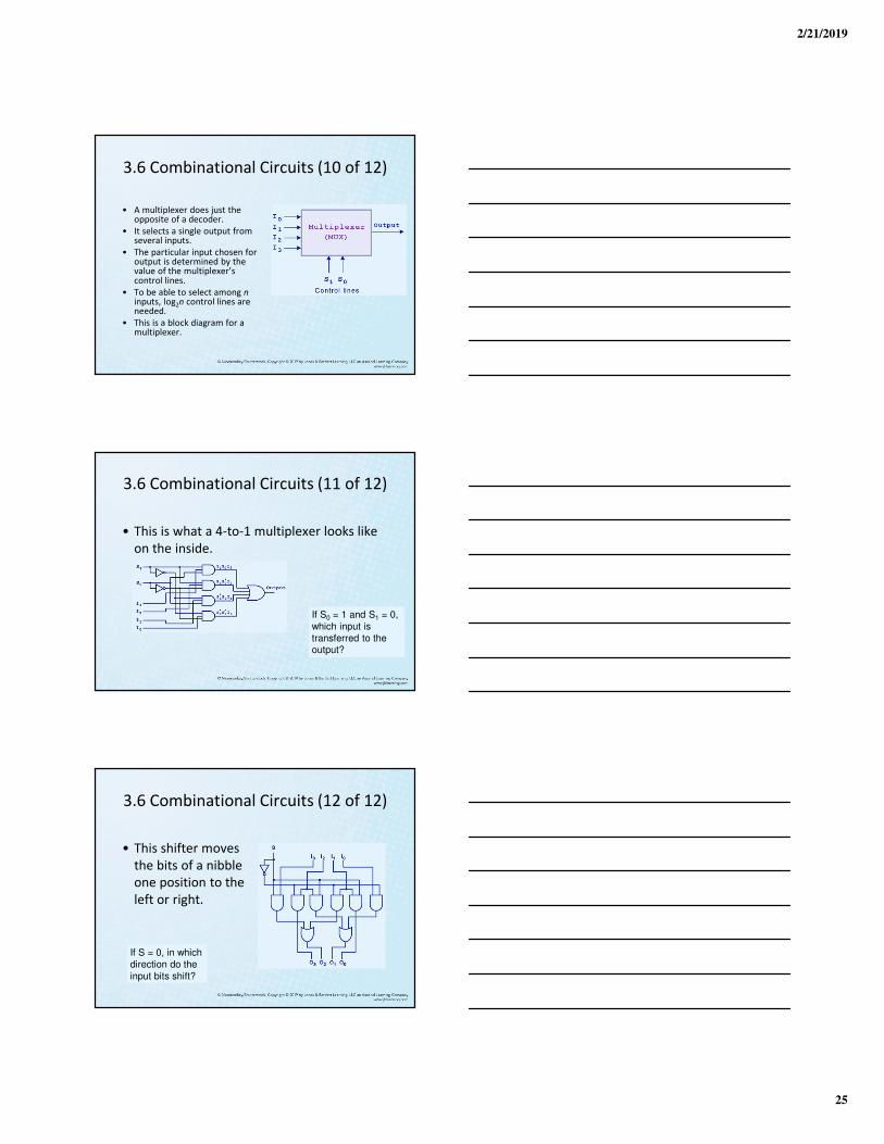
3.6 Combinational Circuits (11 of 12)
• This is what a 4-to-1 multiplexer looks like
on the inside.
If S0 = 1 and S1 = 0,
which input is
transferred to the output?
3.6 Combinational Circuits (12 of 12)
• This shifter moves
the bits of a nibble
one position to the
left or right.
If S = 0, in which
direction do the
input bits shift?

2/21/2019
26
3.7 Sequential Circuits (1 of 30)
• Combinational logic circuits are perfect for situations when we require the immediate application of a Boolean function to a set of inputs.
• There are other times, however, when we need a circuit to change its value with consideration to its current state as well as its inputs.
– These circuits have to “remember” their current state.
• Sequential logic circuits provide this functionality for us.
3.7 Sequential Circuits (2 of 30)
• As the name implies, sequential logic circuits require a means by which events can be sequenced.
• State changes are controlled by clocks.
– A “clock” is a special circuit that sends electrical pulses through a circuit.
• Clocks produce electrical waveforms such as the one shown below.
3.7 Sequential Circuits (3 of 30)
• State changes occur in sequential circuits
only when the clock ticks.
• Circuits can change state on the rising
edge, falling edge, or when the clock pulse
reaches its highest voltage.

2/21/2019
27
3.7 Sequential Circuits (4 of 30)
• Circuits that change state on the rising edge, or falling edge of the clock pulse are called edge-triggered.
• Level-triggered circuits change state when the clock voltage reaches its highest or lowest level.
3.7 Sequential Circuits (5 of 30)
• To retain their state values, sequential circuits rely on feedback.
• Feedback in digital circuits occurs when an output is looped back to the input.
• A simple example of this concept is shown below.– If Q is 0 it will always be 0, if it is 1, it will always be 1.
Why?
3.7 Sequential Circuits (6 of 30)
• You can see how feedback works by
examining the most basic sequential logic
components, the SR flip-flop.
– The “SR” stands for set/reset.
• The internals of an SR flip-flop are shown
below, along with its block diagram.

2/21/2019
28
3.7 Sequential Circuits (7 of 30)
• The behavior of an SR flip-flop is described
by a characteristic table.
• Q(t) means the value of the output at time
t. Q(t+1) is the value of Q after the next
clock pulse.
3.7 Sequential Circuits (8 of 30)
• The SR flip-flop actually has three inputs: S, R, and its current output, Q.
• Thus, we can construct a truth table for this circuit, as shown at the right.
• Notice the two undefined values. When both S and R are 1, the SR flip-flop is unstable.
3.7 Sequential Circuits (9 of 30)
• If we can be sure that the inputs to an SR flip-flop will never both be 1, we will never have an unstable circuit. This may not always be the case.
• The SR flip-flop can be modified to provide a stable state when both inputs are 1.
• This modified flip-flop is called a JK flip-flop, shown at the right.
2/21/2019
29
3.7 Sequential Circuits (10 of 30)
• At the right, we see
how an SR flip-flop
can be modified to
create a JK flip-flop.
• The characteristic
table indicates that
the flip-flop is stable
for all inputs.
3.7 Sequential Circuits (11 of 30)
• Another modification of the SR flip-flop is the D flip-flop, shown below with its characteristic table.
• You will notice that the output of the flip-flop remains the same during subsequent clock pulses. The output changes only when the value of D changes.
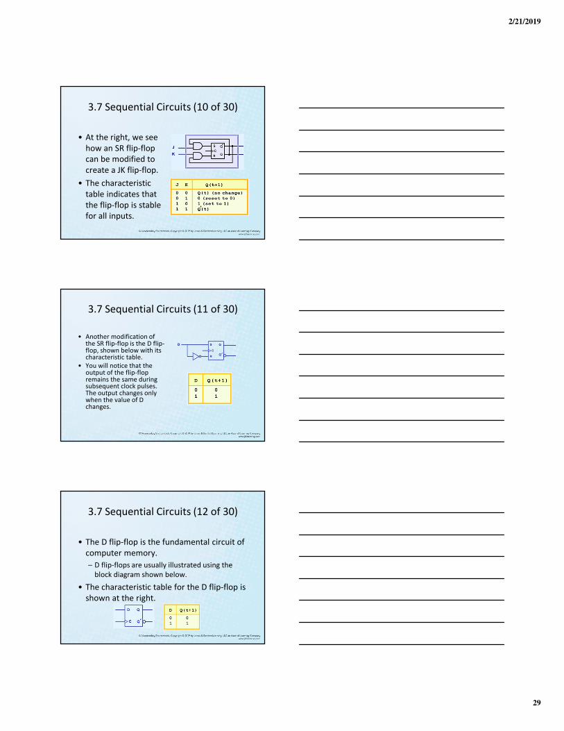
3.7 Sequential Circuits (12 of 30)
• The D flip-flop is the fundamental circuit of
computer memory.
– D flip-flops are usually illustrated using the
block diagram shown below.
• The characteristic table for the D flip-flop is
shown at the right.
2/21/2019
30
3.7 Sequential Circuits (13 of 30)
• The behavior of sequential circuits can be expressed using characteristic tables or finite state machines (FSMs).– FSMs consist of a set of nodes that hold the states of the
machine and a set of arcs that connect the states.
• Moore and Mealy machines are two types of FSMs that are equivalent.– They differ only in how they express the outputs of the
machine.
• Moore machines place outputs on each node, while Mealy machines present their outputs on the transitions.
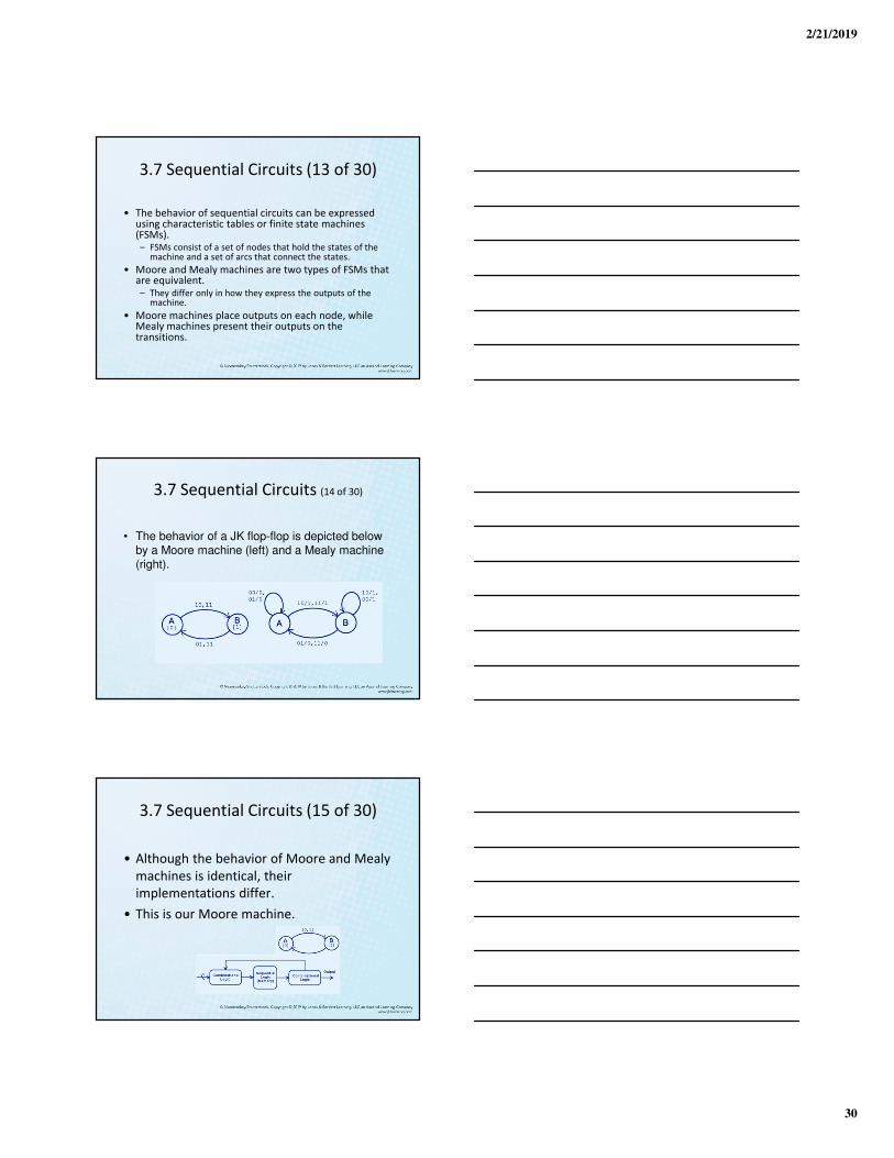
3.7 Sequential Circuits (14 of 30)
• The behavior of a JK flop-flop is depicted below by a Moore machine (left) and a Mealy machine (right).
3.7 Sequential Circuits (15 of 30)
• Although the behavior of Moore and Mealy
machines is identical, their
implementations differ.
• This is our Moore machine.

2/21/2019
31
3.7 Sequential Circuits (16 of 30)
• Although the behavior of Moore and Mealy
machines is identical, their
implementations differ.
• This is our Mealy machine
3.7 Sequential Circuits (17 of 30)
• It is difficult to express the complexities of actual implementations using only Moore and Mealy machines.– For one thing, they do not address the intricacies of timing
very well.
– Secondly, it is often the case that an interaction of numerous signals is required to advance a machine from one state to the next.
• For these reasons, Christopher Clare invented the algorithmic state machine (ASM).
• The next slide illustrates the components of an ASM.
3.7 Sequential Circuits (18 of 30)
2/21/2019
32
3.7 Sequential Circuits (19 of 30)
• This is an ASM for a microwave oven.
3.7 Sequential Circuits (20 of 30)
• Sequential circuits are used anytime that we have a “stateful” application.– A stateful application is one where the next state
of the machine depends on the current state of the machine and the input.
• A stateful application requires both combinational and sequential logic.
• The following slides provide several examples of circuits that fall into this category.
• Can you think of others?
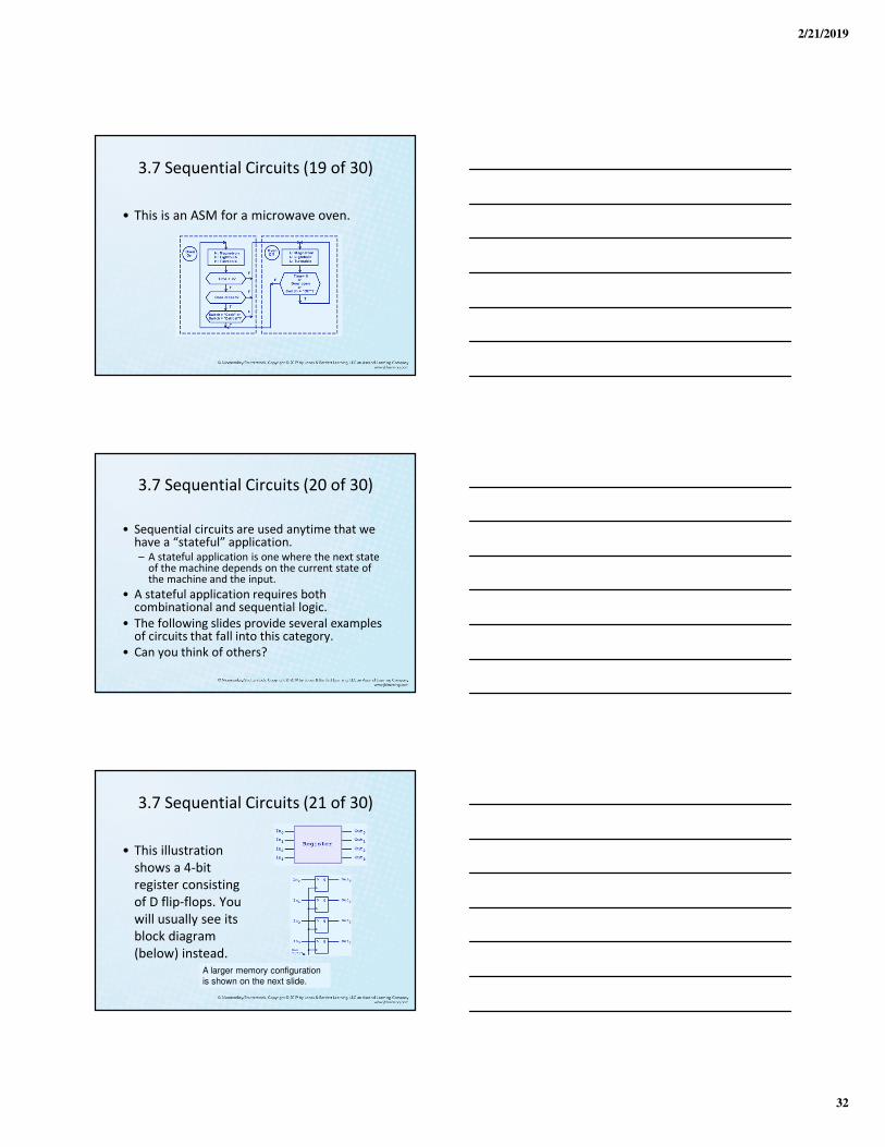
3.7 Sequential Circuits (21 of 30)
• This illustration
shows a 4-bit
register consisting
of D flip-flops. You
will usually see its
block diagram
(below) instead.A larger memory configuration
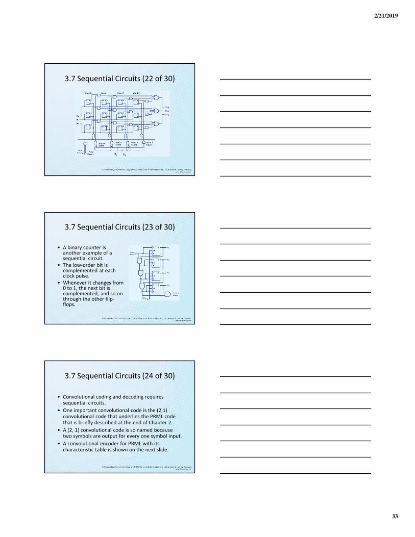
is shown on the next slide.
2/21/2019
33
3.7 Sequential Circuits (22 of 30)
3.7 Sequential Circuits (23 of 30)
• A binary counter is another example of a sequential circuit.
• The low-order bit is complemented at each clock pulse.
• Whenever it changes from 0 to 1, the next bit is complemented, and so on through the other flip-flops.
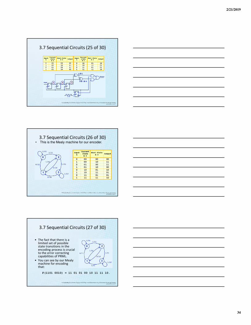
3.7 Sequential Circuits (24 of 30)
• Convolutional coding and decoding requires sequential circuits.
• One important convolutional code is the (2,1) convolutional code that underlies the PRML code that is briefly described at the end of Chapter 2.
• A (2, 1) convolutional code is so named because two symbols are output for every one symbol input.
• A convolutional encoder for PRML with its characteristic table is shown on the next slide.
2/21/2019
34
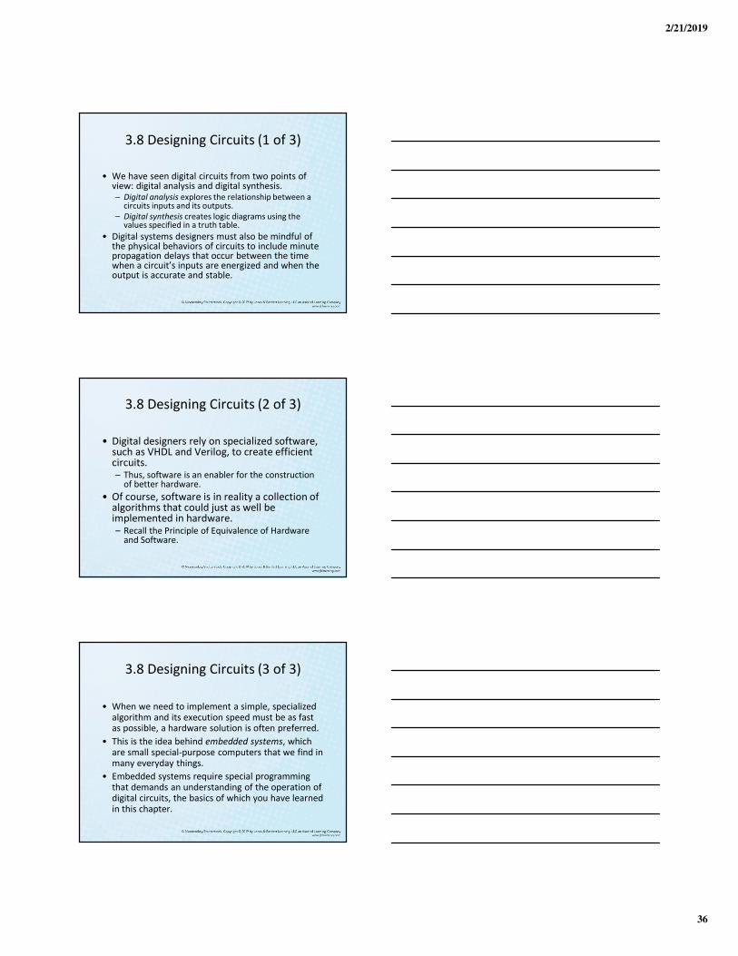
3.7 Sequential Circuits (25 of 30)
• This is the Mealy machine for our encoder.
3.7 Sequential Circuits (26 of 30)
F(1101 0010) = 11 01 01 00 10 11 11 10.
3.7 Sequential Circuits (27 of 30)
• The fact that there is a limited set of possible state transitions in the encoding process is crucial to the error correcting capabilities of PRML.
• You can see by our Mealy machine for encoding that:

2/21/2019
35
F(11 01 01 00 10 11 11 10) = 1101 0010
3.7 Sequential Circuits (28 of 30)
• The decoding of our code is provided by inverting the inputs and outputs of the Mealy machine for the encoding process.
• You can see by our Mealy machine for decoding that:
F(00 10 11 11) = 1001
3.7 Sequential Circuits (29 of 30)
• Yet another way of looking at the decoding process is through a lattice diagram.
• Here we have plotted the state transitions based on the input (top) and showing the output at the bottom for the string 00 10 11 11.
F(00 10 11 11) = 1001
3.7 Sequential Circuits (30 of 30)
• Suppose we receive the erroneous string: 10 10 11 11.
• Here we have plotted the accumulated errors based on the allowable transitions.
• The path of least error outputs 1001, thus 1001 is the string of maximum likelihood.
2/21/2019
36
3.8 Designing Circuits (1 of 3)
• We have seen digital circuits from two points of view: digital analysis and digital synthesis.– Digital analysis explores the relationship between a
circuits inputs and its outputs.
– Digital synthesis creates logic diagrams using the values specified in a truth table.
• Digital systems designers must also be mindful of the physical behaviors of circuits to include minute propagation delays that occur between the time when a circuit’s inputs are energized and when the output is accurate and stable.
3.8 Designing Circuits (2 of 3)
• Digital designers rely on specialized software, such as VHDL and Verilog, to create efficient circuits.– Thus, software is an enabler for the construction
of better hardware.
• Of course, software is in reality a collection of algorithms that could just as well be implemented in hardware.– Recall the Principle of Equivalence of Hardware
and Software.
3.8 Designing Circuits (3 of 3)
• When we need to implement a simple, specialized algorithm and its execution speed must be as fast as possible, a hardware solution is often preferred.
• This is the idea behind embedded systems, which are small special-purpose computers that we find in many everyday things.
• Embedded systems require special programming that demands an understanding of the operation of digital circuits, the basics of which you have learned in this chapter.
2/21/2019
37
Conclusion (1 of 3)
• Computers are implementations of Boolean logic.
• Boolean functions are completely described by truth tables.
• Logic gates are small circuits that implement Boolean operators.
• The basic gates are AND, OR, and NOT.– The XOR gate is very useful in parity checkers and
adders.
• The “universal gates” are NOR, and NAND.
Conclusion (2 of 3)
• Computer circuits consist of combinational logic circuits and sequential logic circuits.
• Combinational circuits produce outputs (almost) immediately when their inputs change.
• Sequential circuits require clocks to control their changes of state.
• The basic sequential circuit unit is the flip-flop: The behaviors of the SR, JK, and D flip-flops are the most important to know.
Conclusion (3 of 3)
• The behavior of sequential circuits can be expressed using characteristic tables or through various finite state machines.
• Moore and Mealy machines are two finite state machines that model high-level circuit behavior.
• Algorithmic state machines are better than Moore and Mealy machines at expressing timing and complex signal interactions.
• Examples of sequential circuits include memory, counters, and Viterbi encoders and decoders.