Chapter 2 Introduction to Logic Circuitskalla/ECE3700/verlogic3_chapter2.pdfFigure 2.10. An example...
80
Chapter 2 Introduction to Logic Circuits
Transcript of Chapter 2 Introduction to Logic Circuitskalla/ECE3700/verlogic3_chapter2.pdfFigure 2.10. An example...

Chapter 2
Introduction to Logic Circuits
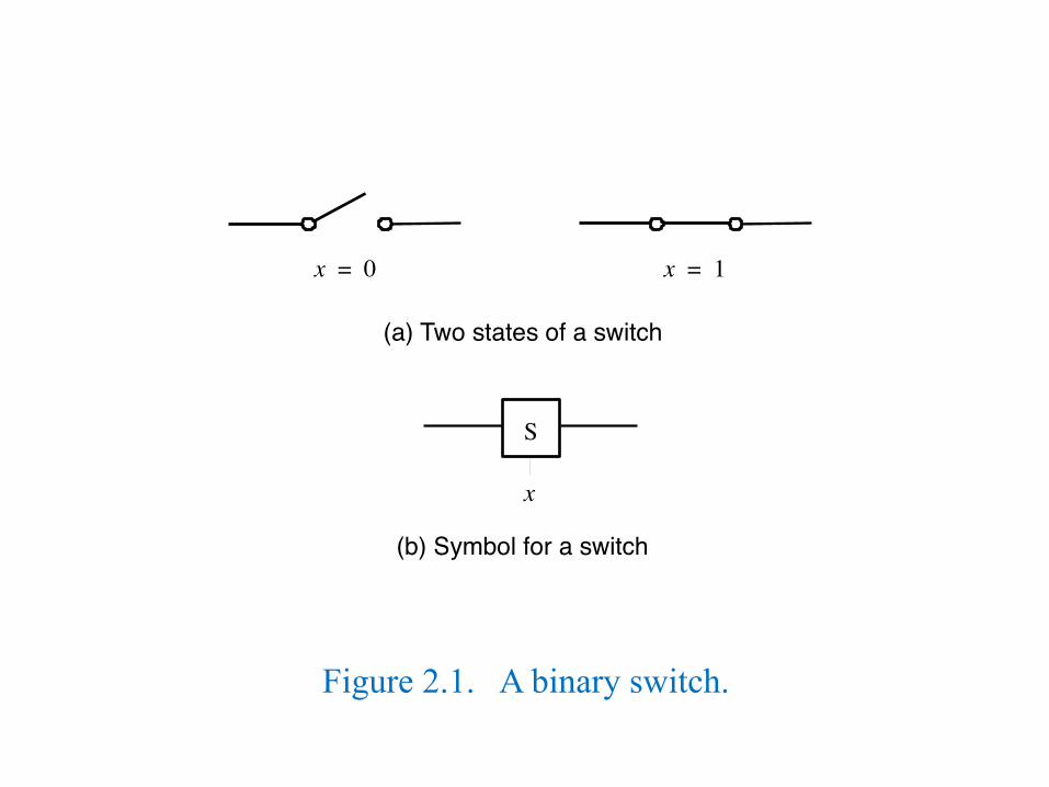
Figure 2.1. A binary switch.
x 1 = x 0 =
(a) Two states of a switch
S
x
(b) Symbol for a switch

Figure 2.2. A light controlled by a switch.
(a) Simple connection to a battery
S
(b) Using a ground connection as the return path
Battery Light
Power supply
S
Light
x
x

Figure 2.3. Two basic functions.
(a) The logical AND function (series connection)
S Power supply
S
S
Power supply S
(b) The logical OR function (parallel connection)
Light
Light x1 x2
x1
x2

Figure 2.4. A series-parallel connection.
S
Power supply S
Light
S
X1
X2
X3
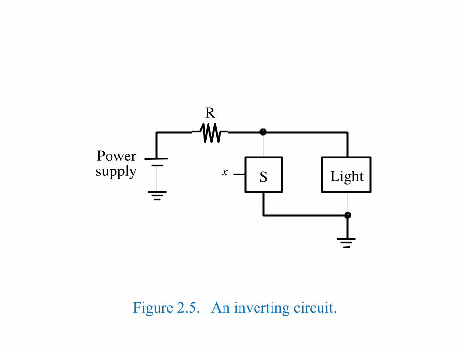
Figure 2.5. An inverting circuit.
S Light Power supply
R
x

Figure 2.6. A truth table for the AND and OR operations.
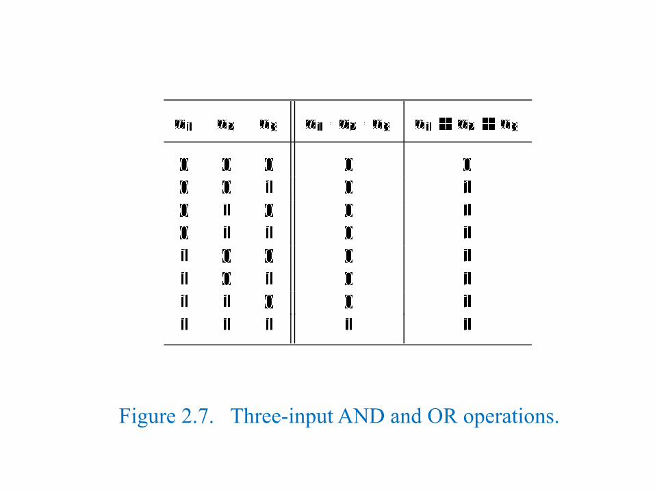
Figure 2.7. Three-input AND and OR operations.

x 1 x 2
x n
x 1 x 2 … x n + + +
x 1 x 2
x 1 x 2 +
x 1 x 2
x n
x 1 x 2
x 1 x 2 ⋅ x 1 x 2
… x n ⋅ ⋅ ⋅
(a) AND gates
(b) OR gates
x x
(c) NOT gateFigure 2.8. The basic gates.

Figure 2.9. The function from Figure 2.4.
x 1 x 2 x 3
f x 1 x 2 + ( ) x 3 ⋅ =

Figure 2.10. An example of logic networks.
Please see “portrait orientation” PowerPoint file for Chapter 2

Figure 2.11. An example of a logic circuit.

Figure 2.12. Addition of binary numbers.

Figure 2.13. Proof of DeMorgan’s theorem in 15a.

Figure 2.14. The Venn diagram representation.
Please see “portrait orientation” PowerPoint file for Chapter 2

Figure 2.15. Verification of the distributive property.
Please see “portrait orientation” PowerPoint file for Chapter 2

Please see “portrait orientation” PowerPoint file for Chapter 2
Figure 2.16. Verification of x y ⋅ x + z y z = ⋅ + ⋅ x y ⋅ x + z.⋅

Figure 2.17. Proof of the distributive property 12b.
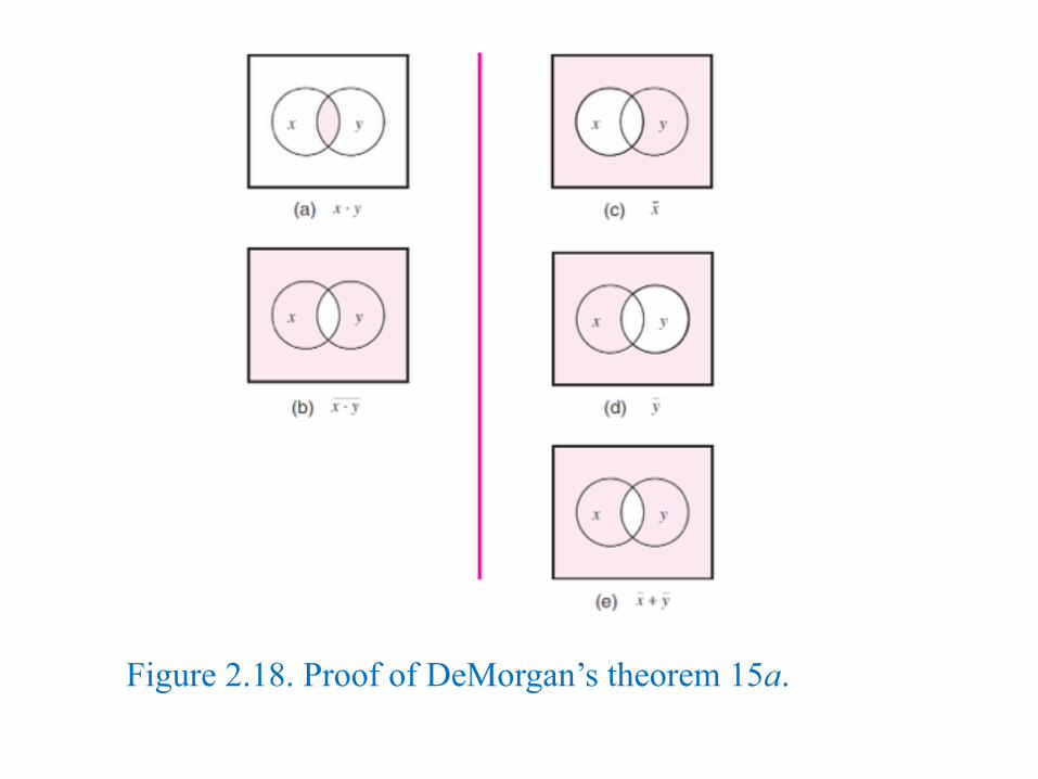
Figure 2.18. Proof of DeMorgan’s theorem 15a.
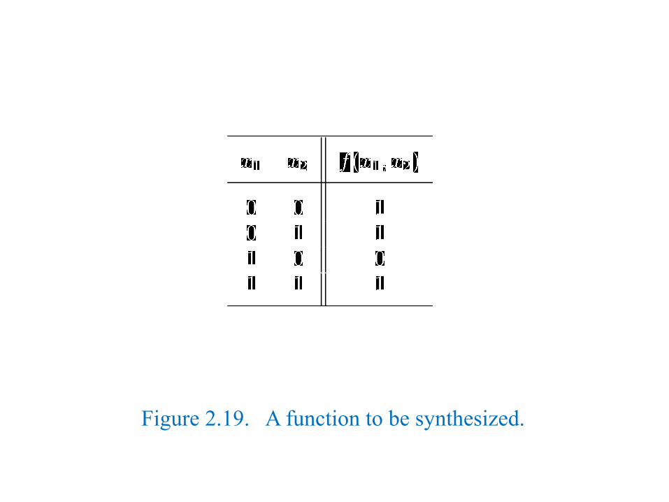
Figure 2.19. A function to be synthesized.

f
(a) Canonical sum-of-products
f
(b) Minimal-cost realization
x 2
x 1
x 1 x 2
Figure 2.20. Two implementations of the function in Figure 2.19.

Figure 2.21. A bubble gumball factory.

Figure 2.22 Three-variable minterms and maxterms.

Figure 2.23. A three-variable function.

Figure 2.24. Two realizations of a function in Figure 2.23.
f
(a) A minimal sum-of-products realization
f
(b) A minimal product-of-sums realization
x1
x2
x3
x2
x1x3
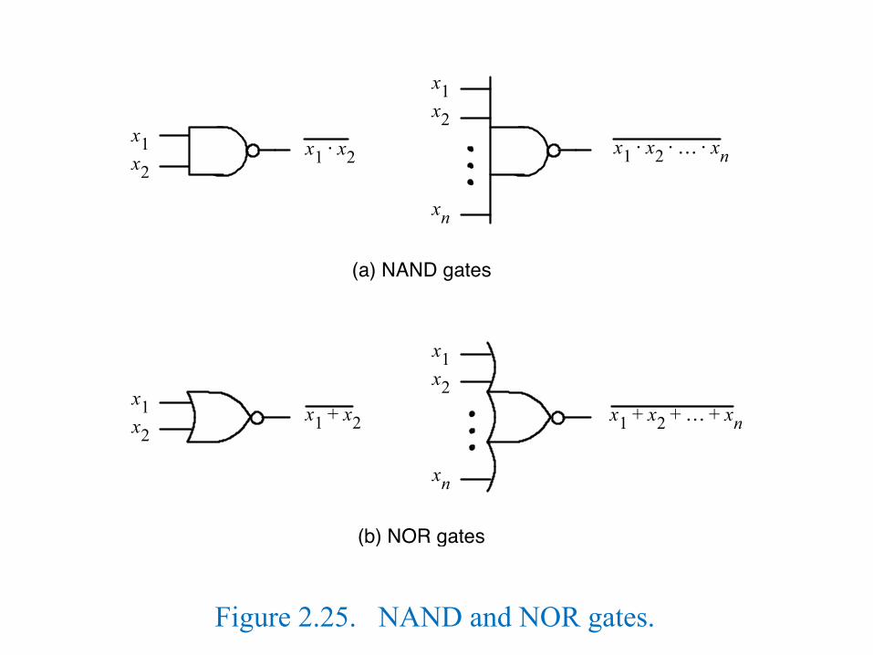
Figure 2.25. NAND and NOR gates.
x 1 x 2
x n
x 1 x 2 … x n + + + x 1 x 2
x 1 x 2 +
x 1 x 2
x n
x 1 x 2
x 1 x 2 ⋅ x 1 x 2 … x n ⋅ ⋅ ⋅
(a) NAND gates
(b) NOR gates

x 1 x 2
x 1
x 2
x 1 x 2
x 1 x 2
x 1
x 2
x 1 x 2
x 1 x 2 x 1 x 2 + = (a)
x 1 x 2 + x 1 x 2 = (b)
Figure 2.26. DeMorgan’s theorem in terms of logic gates.
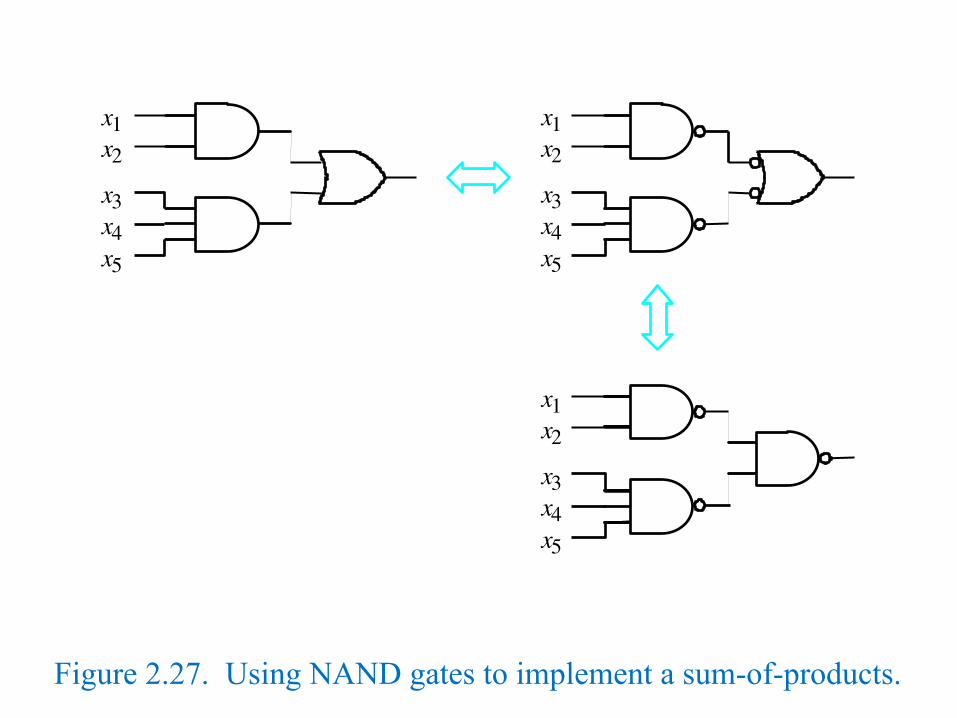
Figure 2.27. Using NAND gates to implement a sum-of-products.
x 1 x 2
x 3 x 4 x 5
x 1 x 2
x 3 x 4 x 5
x 1 x 2
x 3 x 4 x 5

Figure 2.28. Using NOR gates to implement a product-of sums.
x 1 x 2
x 3 x 4 x 5
x 1 x 2
x 3 x 4 x 5
x 1 x 2
x 3 x 4 x 5

Figure 2.29 NOR-gate realization of the function in Example 2.11.
x1
f
(a) POS implementation
(b) NOR implementation
f
x3
x2
x1
x3
x2

Figure 2.30. NAND-gate realization of the function in Example 2.10.
f
f
(a) SOP implementation
(b) NAND implementation
x1
x3
x2
x3
x2
x1

Figure 2.31. Truth table for a three-way light control.
Figure 2.32. Implementation of the function in Figure 2.31.
Please see “portrait orientation” PowerPoint file for Chapter 2

Please see “portrait orientation” PowerPoint file for Chapter 2
Figure 2.33. Implementation of a multiplexer.

Figure 2.34. Display of numbers.

Please see “portrait orientation” PowerPoint file for Chapter 2
Figure 2.35. A typical CAD system.

Figure 2.36. The logic circuit for a multiplexer.

Figure 2.37. Verilog code for the circuit in Figure 2.36.

Figure 2.38. Verilog code for a four-input circuit.
module example2 (x1, x2, x3, x4, f, g, h); input x1, x2, x3, x4; output f, g, h; and (z1, x1, x3); and (z2, x2, x4); or (g, z1, z2); or (z3, x1, ~x3); or (z4, ~x2, x4); and (h, z3, z4); or (f, g, h); endmodule

Figure 2.39. Logic circuit for the code in Figure 2.38.

Figure 2.40. Using the continuous assignment to specify the circuit in Figure 2.36.

Figure 2.41. Using the continuous assignment to specify the circuit in Figure 2.39.
module example4 (x1, x2, x3, x4, f, g, h); input x1, x2, x3, x4; output f, g, h; assign g = (x1 & x3) | (x2 & x4); assign h = (x1 | ~x3) & (~x2 | x4); assign f = g | h; endmodule

Figure 2.42. Behavioral specification of the circuit in Figure 2.36.

Figure 2.43. A more compact version of the code in Figure 2.42.

Figure 2.44. A logic circuit with two modules.

Figure 2.45. Verilog specification of the circuit in Figure 2.12.

Figure 2.46. Verilog specification of the circuit in Figure 2.34.
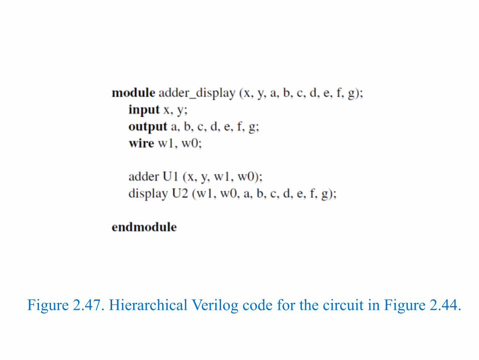
Figure 2.47. Hierarchical Verilog code for the circuit in Figure 2.44.

Figure 2.48 The function f (x1, x2, x3) = Σ m(0, 2, 4, 5, 6).

x 2
(a) Truth table (b) Karnaugh map
0
1
0 1
m 0 m 2
m 3 m 1
x 1 x 2
0 0 0 1 1 0 1 1
m 0 m 1
m 3
m 2
x 1
Figure 2.49. Location of two-variable minterms.

Figure 2.50. The function of Figure 2.19.
x 1 x 2
1 0
1 1 f x 2 x 1 + =
0
1
0 1 1

Figure 2.51. Location of three-variable minterms.
x 1 x 2 x 3 00 01 11 10
0
1
(b) Karnaugh map
x 2 x 3
0 0 0 1 1 0 1 1
m 0 m 1
m 3
m 2
0 0 0 0
0 0 0 1 1 0 1 1
1 1 1 1
m 4 m 5
m 7
m 6
x 1
(a) Truth table
m 0
m 1 m 3
m 2 m 6
m 7
m 4
m 5

Figure 2.52. Examples of three-variable Karnaugh maps.

Figure 2.53. A four-variable Karnaugh map.
x 1 x 2 x 3 x 4 00 01 11 10
00
01
11
10
x 2
x 4
x 1
x 3
m 0
m 1 m 5
m 4 m 12
m 13
m 8
m 9
m 3
m 2 m 6
m 7 m 15
m 14
m 11
m 10
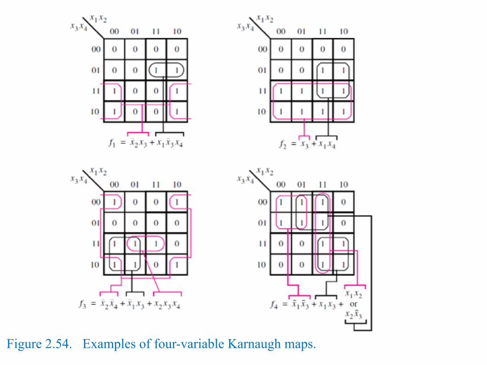
Figure 2.54. Examples of four-variable Karnaugh maps.
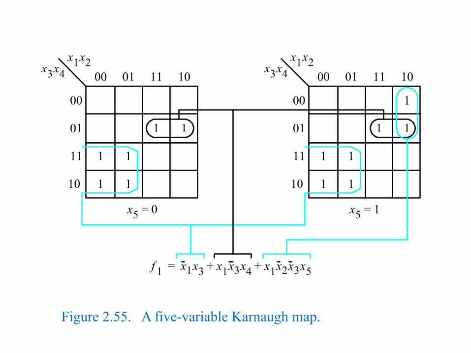
Figure 2.55. A five-variable Karnaugh map.
x 1 x 2 x 3 x 4 00 01 11 10
1 1
1 1
1 1
00
01
11
10
x 1 x 2 x 3 x 4 00 01 11 10
1
1 1
1 1
1 1
00
01
11
10
f 1 x 1 x 3 x 1 x 3 x 4 x 1 x 2 x 3 x 5 + + =
x 5 1 = x 5 0 =

Figure 2.56. Three-variable function f (x1, x2, x3) = Σ m(0, 1, 2, 3, 7).
x 1 x 2 x 3
1 1
1 1
x 1
0 0
1 0
00 01 11 10
0
1
x 2 x 3

Figure 2.57. Four-variable function f ( x1,…, x4) = Σ m(2, 3, 5, 6, 7, 10, 11, 13, 14).
x 1 x 2 x 3 x 4 00 01 11 10
1 1
1 1
1 1
00
01
11
10
x 1 x 3
1 1
1
x 3 x 4
x 1 x 2 x 4
x 2 x 3
x 2 x 3 x 4

Figure 2.58. The function f ( x1,…, x4) = Σ m(0, 4, 8, 10, 11, 12, 13, 15).
x 1 x 2 x 3 x 4 00 01 11 10
1
1 1 1 1
1
00
01
11
10
x 1 x 2 x 4
1
1
x 3 x 4
x 1 x 2 x 4
x 1 x 2 x 3
x 1 x 2 x 3
x 1 x 3 x 4

Figure 2.59. The function f ( x1,…, x4) = Σ m(0, 2, 4, 5, 10, 11, 13, 15).
x 1 x 2 x 3 x 4 00 01 11 10
1
1
1
1
1
1
00
01
11
10 1
1
x 1 x 3 x 4
x 2 x 3 x 4
x 2 x 3 x 4
x 1 x 3 x 4
x 1 x 2 x 4 x 1 x 2 x 4
x 1 x 2 x 3 x 1 x 2 x 3

Figure 2.60. POS minimization of f (x1, x2, x3) = Π M(4, 5, 6).
x 1 x 2 x 3
1
00 01 11 10
0
1
1 0 0
1 1 1 0
x 1 x 2 + ( )
x 1 x 3 + ( )

Figure 2.61. POS minimization of f ( x1,…, x4) = Π M(0, 1, 4, 8, 9, 12, 15).
x 1 x 2 x 3 x 4
0
00 01 11 10
0 0 0
0 1 1 0
1 1 0 1
1 1 1 1
00
01
11
10
x 2 x 3 + ( )
x 3 x 4 + ( )
x 1 x 2 x 3 x 4 + + + ( )

Figure 2.62. Two implementations of the function f ( x1,…, x4) = Σ m(2, 4, 5, 6, 10) + D(12, 13, 14, 15).
Please see “portrait orientation” PowerPoint file for Chapter 2
Figure 2.63. Using don’t-care minterms when displaying BCD numbers.
Please see “portrait orientation” PowerPoint file for Chapter 2

Figure 2.64. An example of multiple-output synthesis.
Please see “portrait orientation” PowerPoint file for Chapter 2

Figure 2.65. Another example of multiple-output synthesis.
Please see “portrait orientation” PowerPoint file for Chapter 2

Figure 2.66. The Venn diagrams for Example 2.23.
(a) Function A (b) Function B
(c) Function C (d) Function f
x1
x3
x2 x1 x2
x1 x2 x1 x2
x3 x3
x3

Figure 2.67. Karnaugh maps for Example 2.26.
Please see “portrait orientation” PowerPoint file for Chapter 2

Figure 2.68. Karnaugh maps for Example 2.27.
Please see “portrait orientation” PowerPoint file for Chapter 2

Figure 2.69. A K-map that represents the function in Example 2.28.
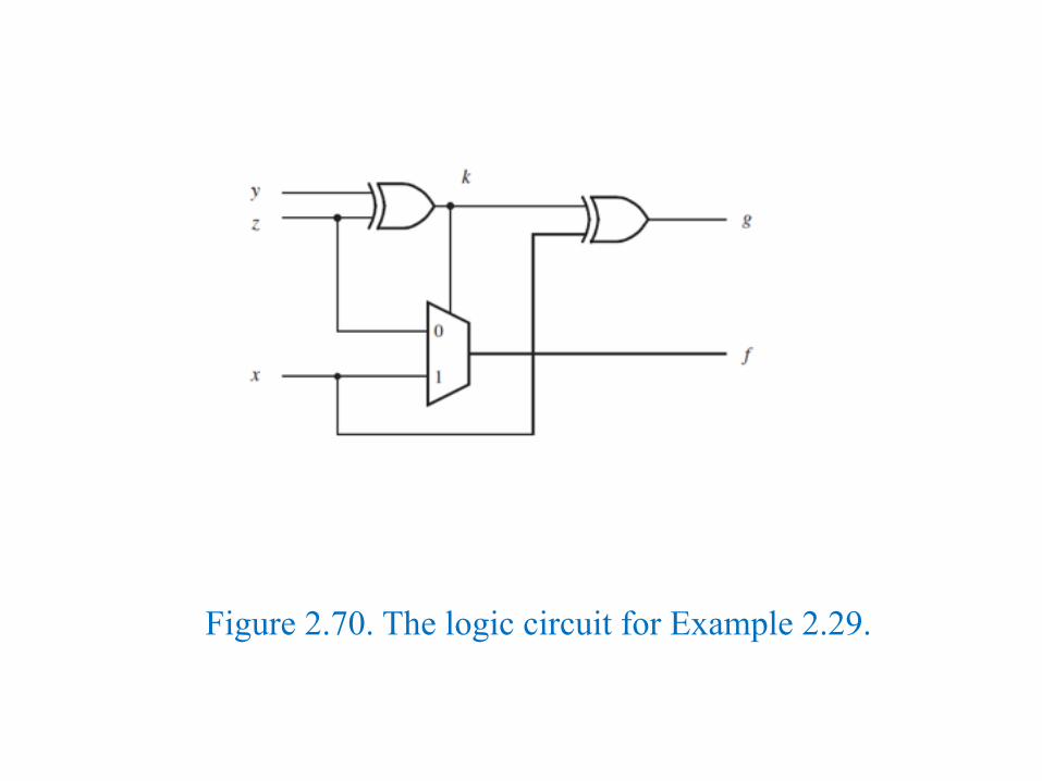
Figure 2.70. The logic circuit for Example 2.29.

Figure 2.70. Verilog code for Example 2.29.

Figure 2.72. The circuit for Example 2.30.

Figure 2.73. Verilog code for Example 2.30.

x 1 x 2
x 3
x 4
(a)
x 1 x 2
x 3
x 4
(b)
Figure P2.1. Two attempts to draw a four-variable Venn diagram.

x 3
x 2 x 1
x 4
x 3
x 2 x 1
m 0
m 1 m 2
Figure P2.2. A four-variable Venn diagram.

Figure P2.3. A timing diagram representing a logic function.
1 0
1 0
1 0
1 0
x 1
x 2
Time
x 3
f

1 0
1 0
1 0
1 0
x 1
x 2
Time
x 3
f
Figure P2.4. A timing diagram representing a logic function.

Figure P2.5. Circuit for problem 2.78.
Please see “portrait orientation” PowerPoint file for Chapter 2

Figure P2.6. Circuit for problem 2.79.
Please see “portrait orientation” PowerPoint file for Chapter 2