Chapter 14 Inductor Designecee.colorado.edu/~ecen5797/course_material/Ch14slides.pdf ·...
42
Fundamentals of Power Electronics Chapter 14: Inductor design 1 Chapter 14 Inductor Design 14.1 Filter inductor design constraints 14.2 A step-by-step design procedure 14.3 Multiple-winding magnetics design using the K g method 14.4 Examples 14.5 Summary of key points
Transcript of Chapter 14 Inductor Designecee.colorado.edu/~ecen5797/course_material/Ch14slides.pdf ·...

Fundamentals of Power Electronics Chapter 14: Inductor design1
Chapter 14 Inductor Design
14.1 Filter inductor design constraints
14.2 A step-by-step design procedure
14.3 Multiple-winding magnetics design using theKg method
14.4 Examples
14.5 Summary of key points
Fundamentals of Power Electronics Chapter 14: Inductor design2
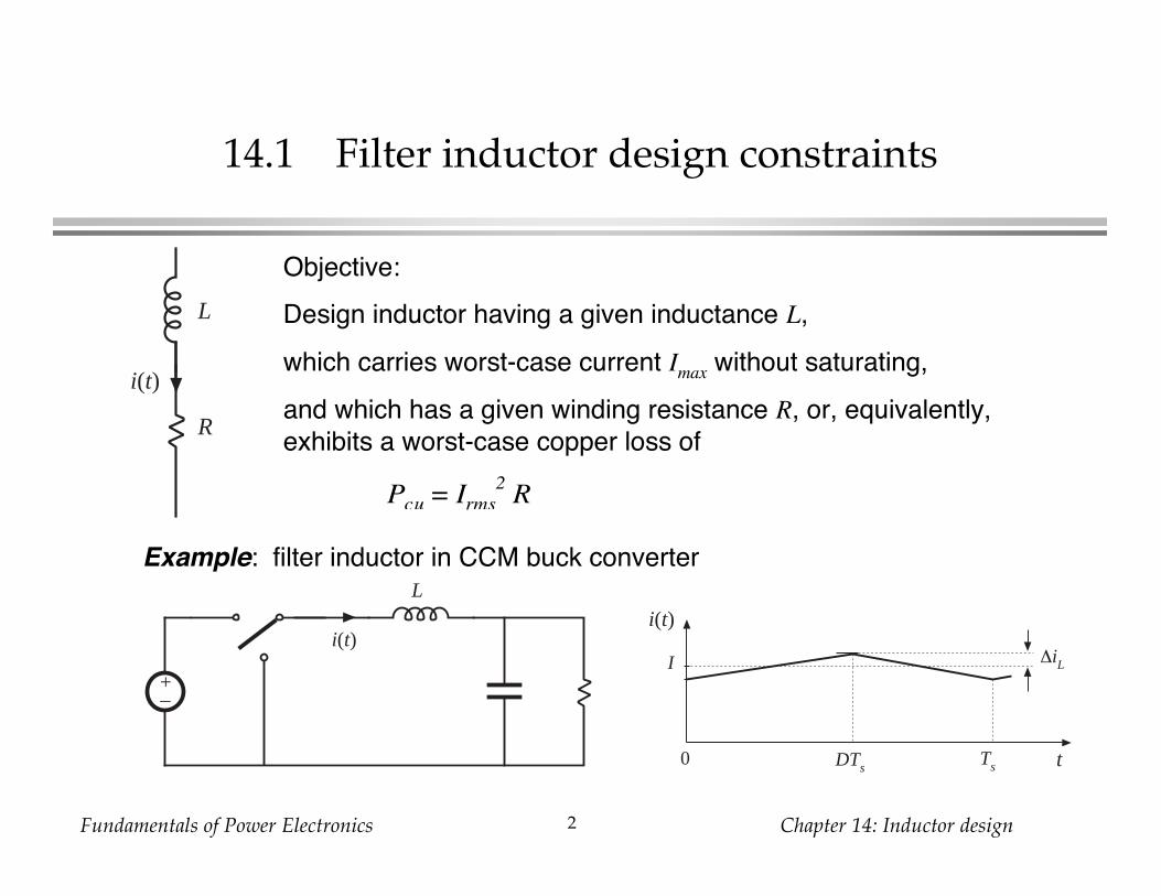
14.1 Filter inductor design constraints
Pcu
= Irms
2 R
Objective:
Design inductor having a given inductance L,
which carries worst-case current Imax without saturating,
and which has a given winding resistance R, or, equivalently,
exhibits a worst-case copper loss of
L
R
i(t)
+–
L
i(t)i(t)
t0 DTsTs
I ∆iL
Example: filter inductor in CCM buck converter
Fundamentals of Power Electronics Chapter 14: Inductor design3
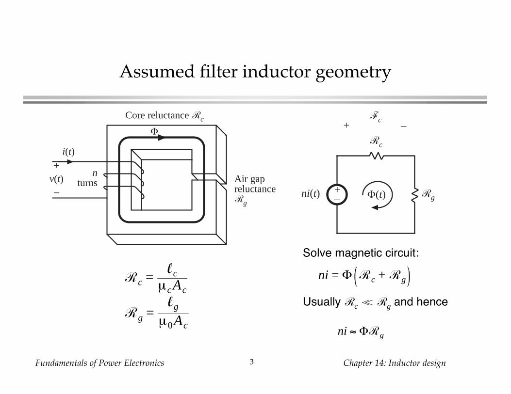
Assumed filter inductor geometry
Solve magnetic circuit:
Air gapreluctanceRg
nturns
i(t)
Φ
Core reluctance Rc
+v(t)– +
–ni(t) Φ(t)
Rc
Rg
Fc+ –
Rc =lc
µcAc
Rg =lg
µ0Ac
ni = Φ Rc + Rg
ni ≈ ΦRg
Usually Rc < Rg and hence
Fundamentals of Power Electronics Chapter 14: Inductor design4
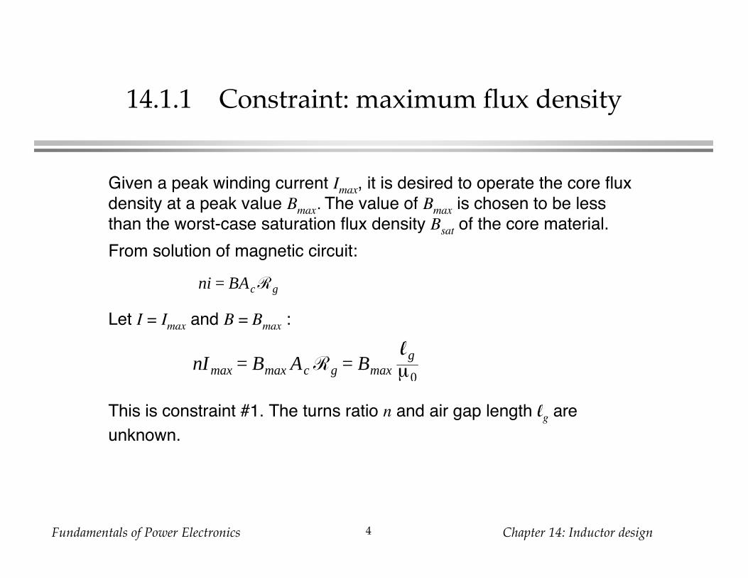
14.1.1 Constraint: maximum flux density
Given a peak winding current Imax, it is desired to operate the core flux
density at a peak value Bmax. The value of Bmax is chosen to be less
than the worst-case saturation flux density Bsat of the core material.
From solution of magnetic circuit:
Let I = Imax and B = Bmax :
This is constraint #1. The turns ratio n and air gap length lg are
unknown.
ni = BAcRg
nImax = Bmax AcRg = Bmax
lgµ0
Fundamentals of Power Electronics Chapter 14: Inductor design5
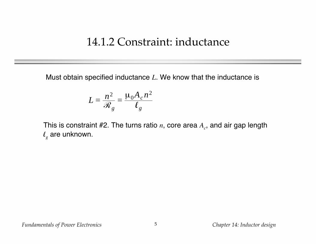
14.1.2 Constraint: inductance
Must obtain specified inductance L. We know that the inductance is
This is constraint #2. The turns ratio n, core area Ac, and air gap length
lg are unknown.
L = n2
Rg=µ0Ac n2
lg
Fundamentals of Power Electronics Chapter 14: Inductor design6
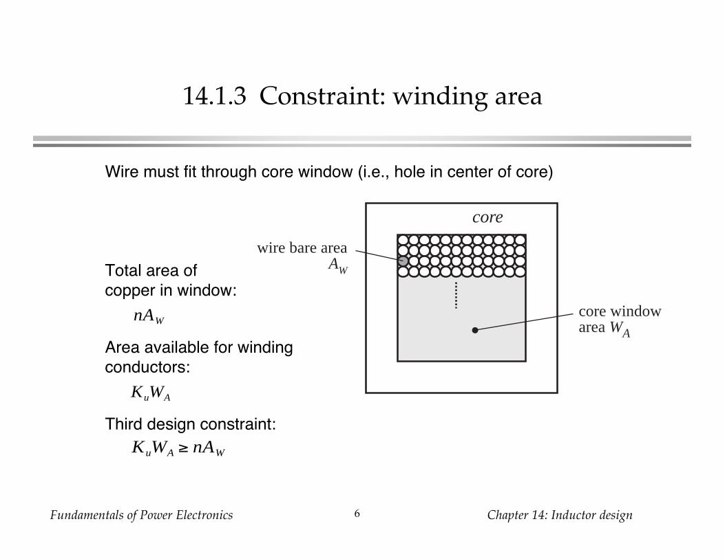
14.1.3 Constraint: winding area
core windowarea WA
wire bare areaAW
core
Wire must fit through core window (i.e., hole in center of core)
nAW
Total area of
copper in window:
KuWA
Area available for winding
conductors:
Third design constraint:
KuWA ≥ nAW

Fundamentals of Power Electronics Chapter 14: Inductor design7
The window utilization factor Kualso called the “fill factor”
Ku is the fraction of the core window area that is filled by copper
Mechanisms that cause Ku to be less than 1:
• Round wire does not pack perfectly, which reduces Ku by a
factor of 0.7 to 0.55 depending on winding technique
• Insulation reduces Ku by a factor of 0.95 to 0.65, depending on
wire size and type of insulation
• Bobbin uses some window area
• Additional insulation may be required between windings
Typical values of Ku :
0.5 for simple low-voltage inductor
0.25 to 0.3 for off-line transformer
0.05 to 0.2 for high-voltage transformer (multiple kV)
0.65 for low-voltage foil-winding inductor
Fundamentals of Power Electronics Chapter 14: Inductor design8
14.1.4 Winding resistance
The resistance of the winding is
where is the resistivity of the conductor material, lb is the length of
the wire, and AW is the wire bare area. The resistivity of copper atroom temperature is 1.724 10–6 -cm. The length of the wire comprising
an n-turn winding can be expressed as
where (MLT) is the mean-length-per-turn of the winding. The mean-
length-per-turn is a function of the core geometry. The above
equations can be combined to obtain the fourth constraint:
R = ρn (MLT)
AW
R = ρlb
AW
lb = n (MLT )
Fundamentals of Power Electronics Chapter 14: Inductor design9
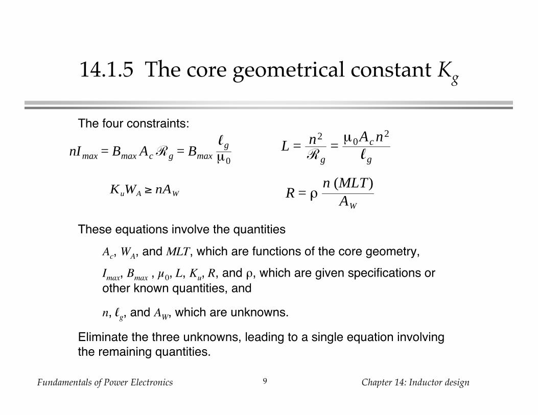
14.1.5 The core geometrical constant Kg
The four constraints:
R = ρn (MLT)
AW
KuWA ≥ nAW
These equations involve the quantities
Ac, WA, and MLT, which are functions of the core geometry,
Imax, Bmax , µ0, L, Ku, R, and , which are given specifications or
other known quantities, and
n, lg, and AW, which are unknowns.
Eliminate the three unknowns, leading to a single equation involving
the remaining quantities.
nImax = Bmax AcRg = Bmax
lgµ0
L = n2
Rg=µ0Ac n2
lg

Fundamentals of Power Electronics Chapter 14: Inductor design10
Core geometrical constant Kg
Ac2WA
(MLT)≥
ρL2I max2
Bmax2 RKu
Elimination of n, lg, and AW leads to
• Right-hand side: specifications or other known quantities
• Left-hand side: function of only core geometry
So we must choose a core whose geometry satisfies the above
equation.
The core geometrical constant Kg is defined as
Kg =Ac
2WA
(MLT)
Fundamentals of Power Electronics Chapter 14: Inductor design11
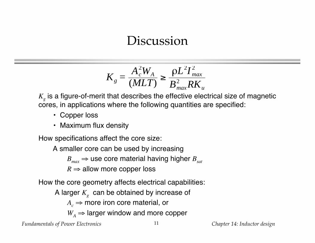
Discussion
Kg =Ac
2WA
(MLT)≥
ρL2I max2
Bmax2 RKu
Kg is a figure-of-merit that describes the effective electrical size of magnetic
cores, in applications where the following quantities are specified:
• Copper loss
• Maximum flux density
How specifications affect the core size:
A smaller core can be used by increasing
Bmax use core material having higher Bsat
R allow more copper loss
How the core geometry affects electrical capabilities:
A larger Kg can be obtained by increase of
Ac more iron core material, or
WA larger window and more copper
Fundamentals of Power Electronics Chapter 14: Inductor design12
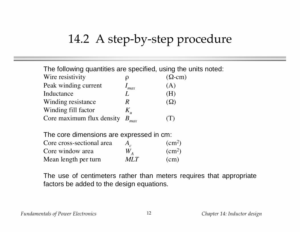
14.2 A step-by-step procedure
The following quantities are specified, using the units noted:Wire resistivity ( -cm)
Peak winding current Imax (A)
Inductance L (H)
Winding resistance R ( )
Winding fill factor Ku
Core maximum flux density Bmax (T)
The core dimensions are expressed in cm:Core cross-sectional area Ac (cm2)
Core window area WA (cm2)
Mean length per turn MLT (cm)
The use of centimeters rather than meters requires that appropriatefactors be added to the design equations.
Fundamentals of Power Electronics Chapter 14: Inductor design13
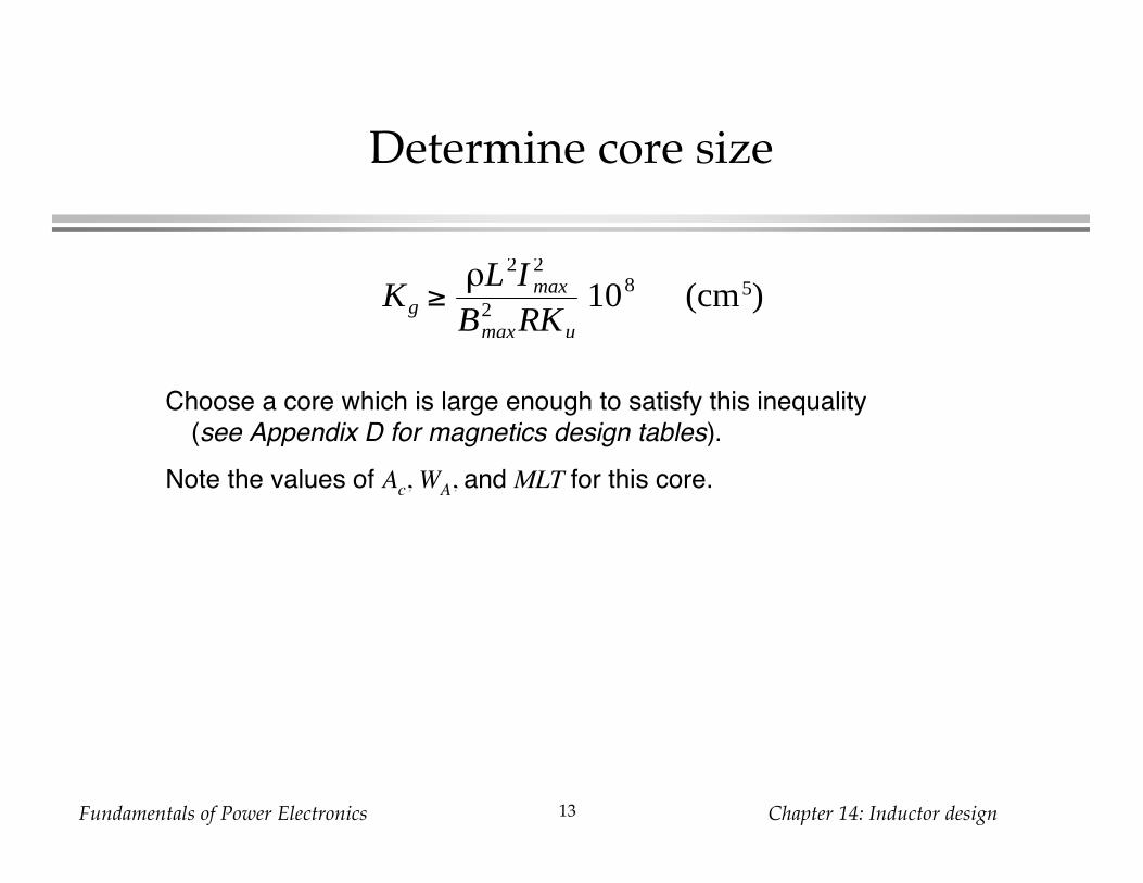
Determine core size
Kg ≥ρL2I max
2
Bmax2 RKu
108 (cm5)
Choose a core which is large enough to satisfy this inequality
(see Appendix D for magnetics design tables).
Note the values of Ac, WA, and MLT for this core.
Fundamentals of Power Electronics Chapter 14: Inductor design14
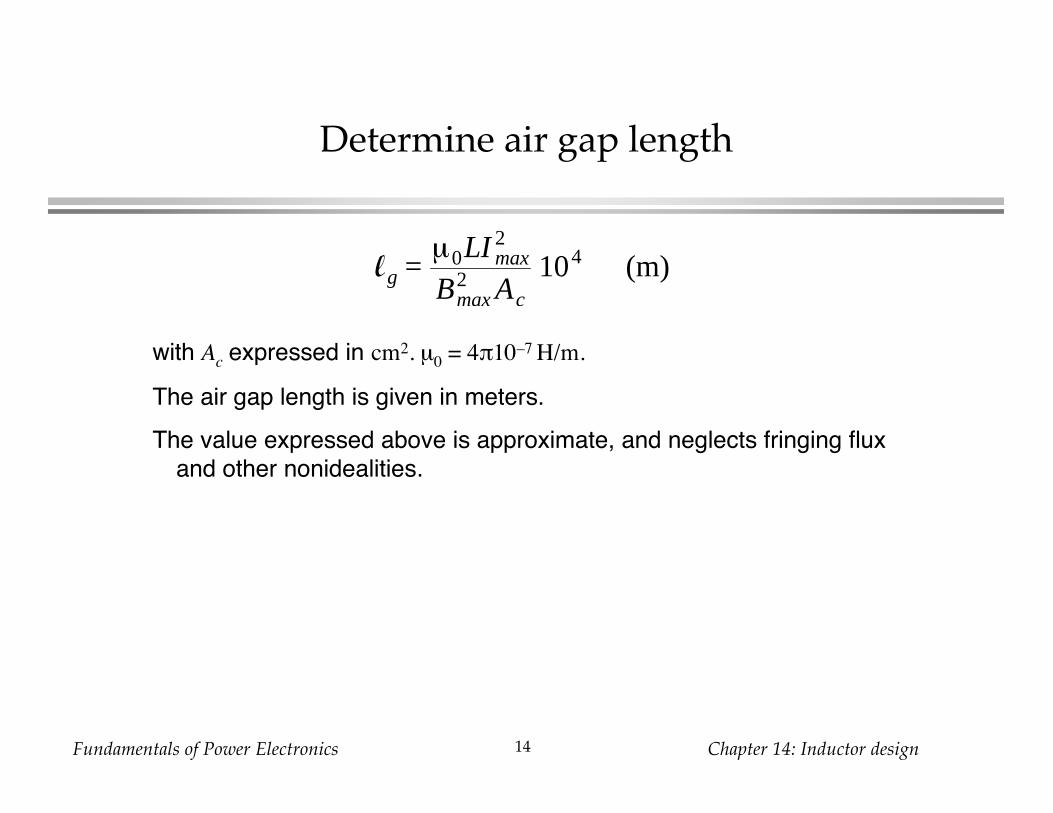
Determine air gap length
with Ac expressed in cm2. µ0 = 4 10–7 H/m.
The air gap length is given in meters.
The value expressed above is approximate, and neglects fringing flux
and other nonidealities.
lg =µ0LI max
2
Bmax2 Ac
104 (m)
Fundamentals of Power Electronics Chapter 14: Inductor design15
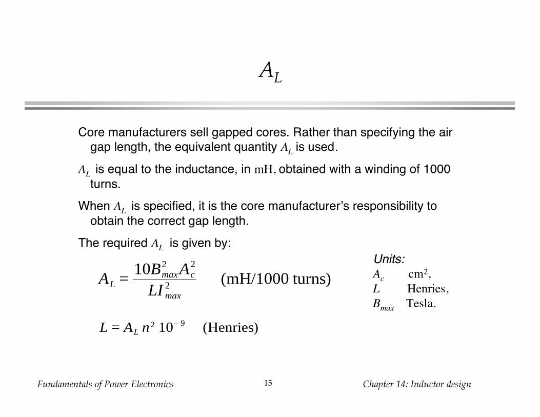
AL
Core manufacturers sell gapped cores. Rather than specifying the airgap length, the equivalent quantity AL is used.
AL is equal to the inductance, in mH, obtained with a winding of 1000
turns.
When AL is specified, it is the core manufacturer’s responsibility to
obtain the correct gap length.
The required AL is given by:
AL =10Bmax
2 Ac2
LI max2 (mH/1000 turns)
L = AL n2 10– 9 (Henries)
Units:Ac cm2,
L Henries,
Bmax Tesla.
Fundamentals of Power Electronics Chapter 14: Inductor design16
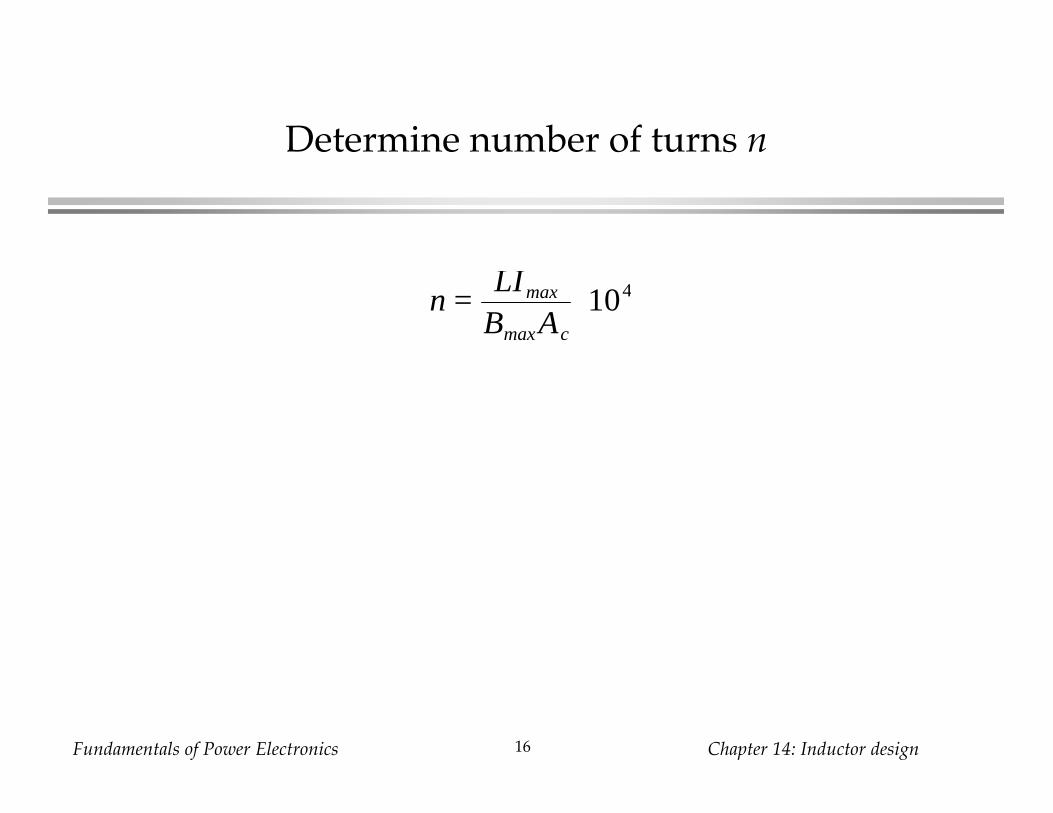
Determine number of turns n
n =LImax
BmaxAc
104
Fundamentals of Power Electronics Chapter 14: Inductor design17
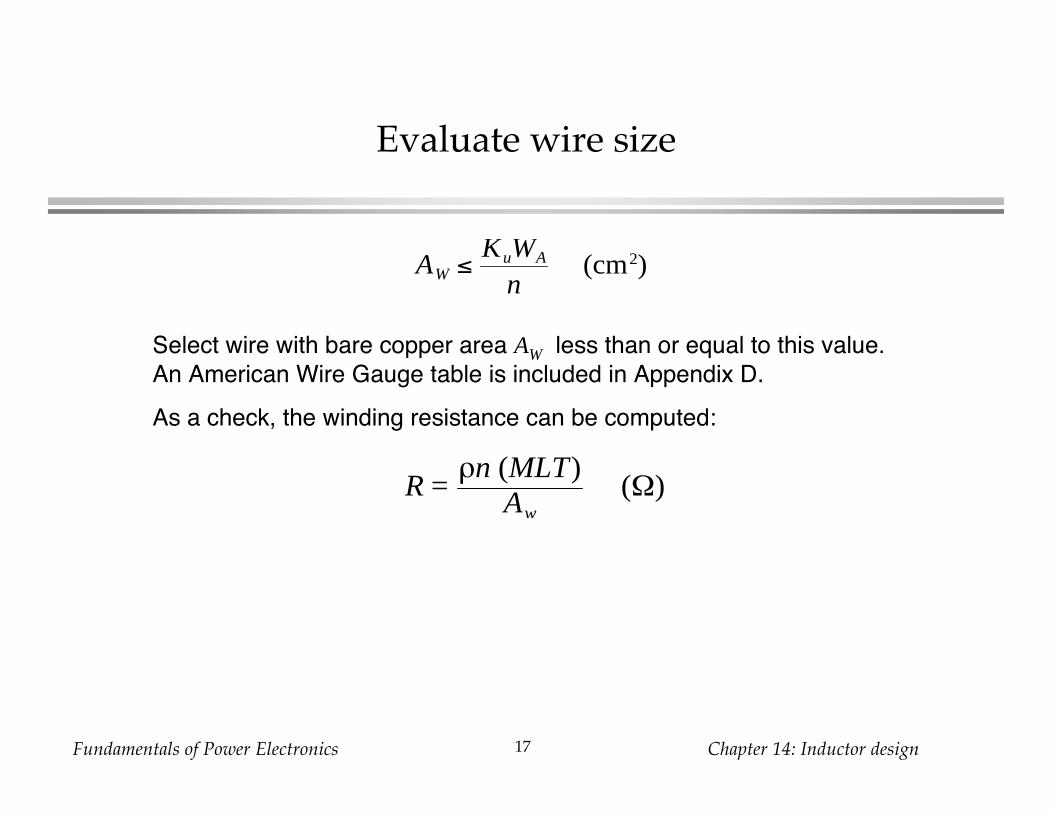
Evaluate wire size
AW ≤KuWA
n(cm2)
Select wire with bare copper area AW less than or equal to this value.
An American Wire Gauge table is included in Appendix D.
As a check, the winding resistance can be computed:
R =ρn (MLT)
Aw(Ω)
Fundamentals of Power Electronics Chapter 14: Inductor design18
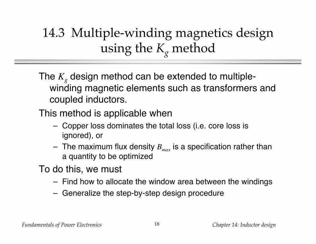
14.3 Multiple-winding magnetics designusing the Kg method
The Kg design method can be extended to multiple-
winding magnetic elements such as transformers andcoupled inductors.
This method is applicable when
– Copper loss dominates the total loss (i.e. core loss is
ignored), or
– The maximum flux density Bmax is a specification rather than
a quantity to be optimized
To do this, we must
– Find how to allocate the window area between the windings
– Generalize the step-by-step design procedure
Fundamentals of Power Electronics Chapter 14: Inductor design19
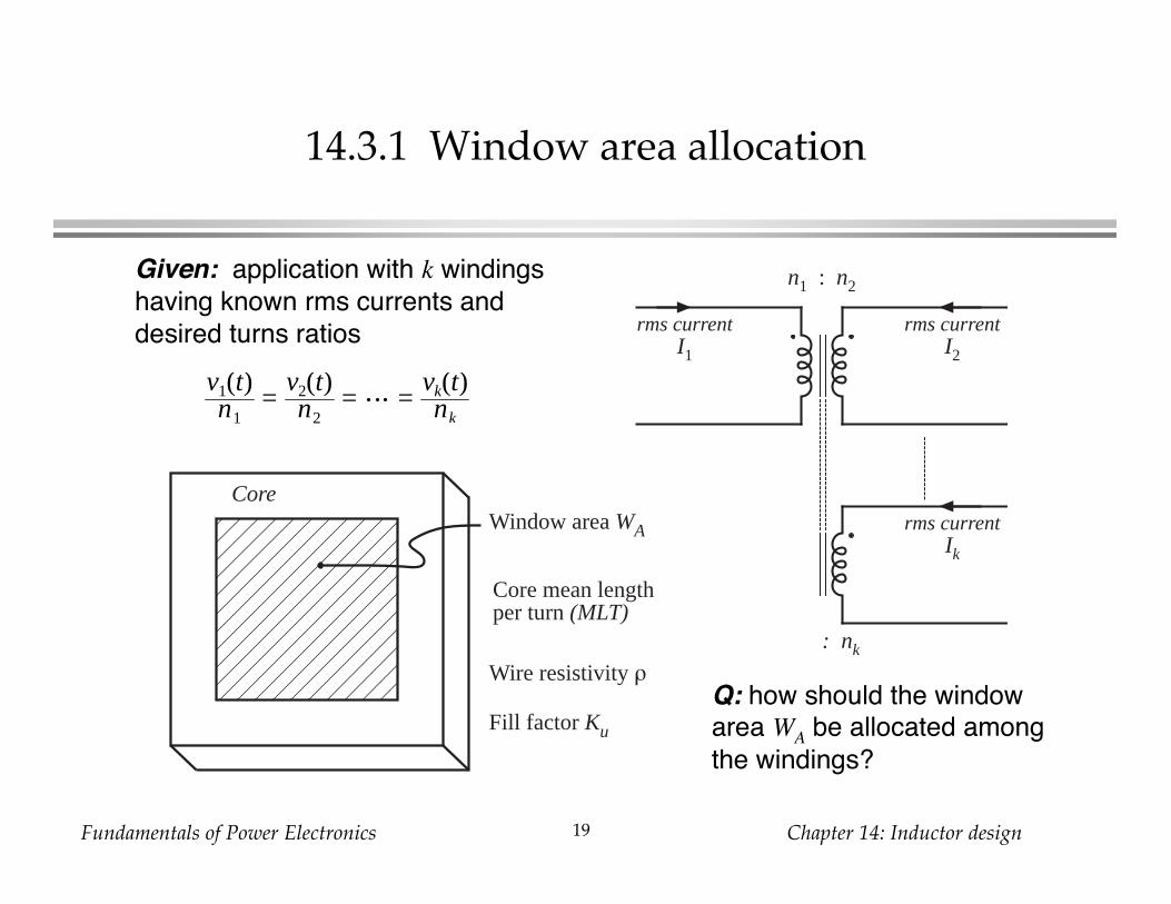
14.3.1 Window area allocation
n1 : n2
: nk
rms currentI1
rms currentI2
rms currentIk
v1(t)n1
=v2(t)n2
= =vk(t)nk
CoreWindow area WA
Core mean lengthper turn (MLT)
Wire resistivity ρ
Fill factor Ku
Given: application with k windings
having known rms currents and
desired turns ratios
Q: how should the windowarea WA be allocated among
the windings?

Fundamentals of Power Electronics Chapter 14: Inductor design20
Allocation of winding area
Total windowarea WA
Winding 1 allocationα1WA
Winding 2 allocationα2WA
etc.
0 < α j < 1
α1 + α2 + + αk = 1
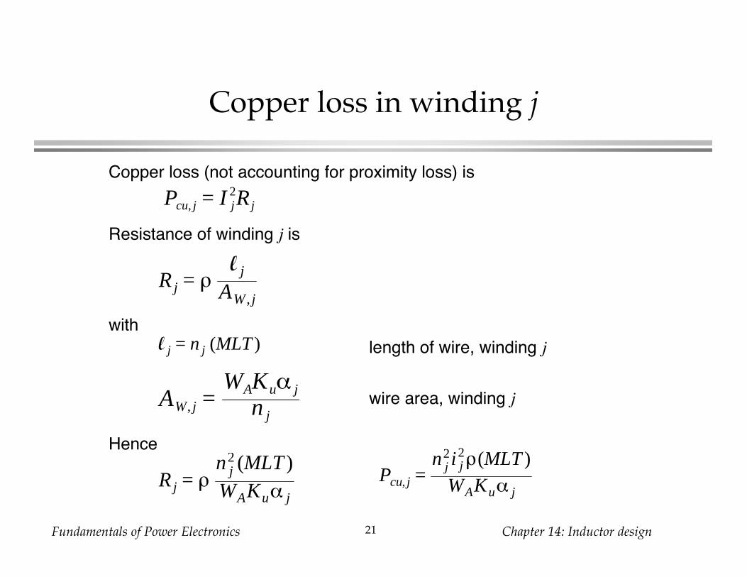
Fundamentals of Power Electronics Chapter 14: Inductor design21
Copper loss in winding j
Copper loss (not accounting for proximity loss) is
Pcu, j = I j2Rj
Resistance of winding j is
with
AW, j =WAKuα j
n j
length of wire, winding j
wire area, winding j
Hence
Rj = ρl j
AW , j
l j = n j (MLT )
Rj = ρn j
2 (MLT )WAKuα j
Pcu, j =n j
2i j2ρ(MLT )
WAKuα j
Fundamentals of Power Electronics Chapter 14: Inductor design22
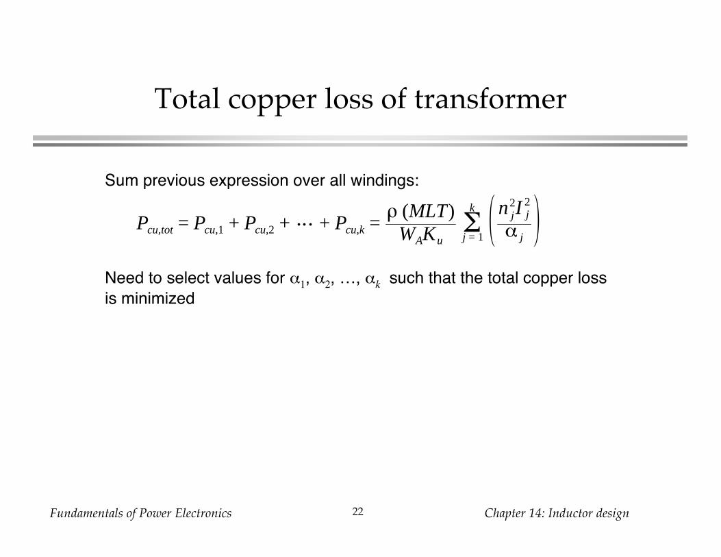
Total copper loss of transformer
Sum previous expression over all windings:
Pcu,tot = Pcu,1 + Pcu,2 + + Pcu,k =ρ (MLT)
WAKu
n j2I j
2
α jΣj = 1
k
Need to select values for 1, 2, …, k such that the total copper loss
is minimized
Fundamentals of Power Electronics Chapter 14: Inductor design23
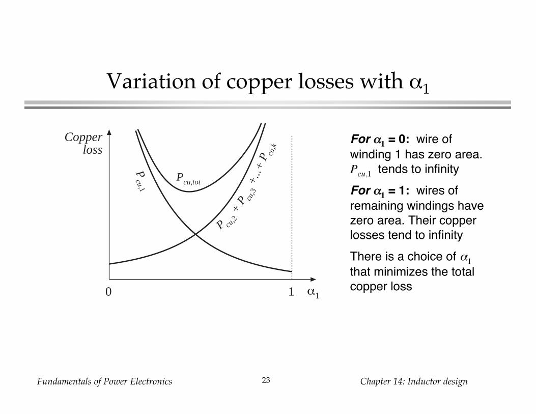
Variation of copper losses with 1
For 1 = 0: wire of
winding 1 has zero area.
Pcu,1 tends to infinity
For 1 = 1: wires of
remaining windings have
zero area. Their copper
losses tend to infinity
There is a choice of 1
that minimizes the total
copper lossα1
Copperloss
0 1
Pcu,tot
Pcu,1
P cu,2+
P cu,3
+...
+P cu
,k
Fundamentals of Power Electronics Chapter 14: Inductor design24
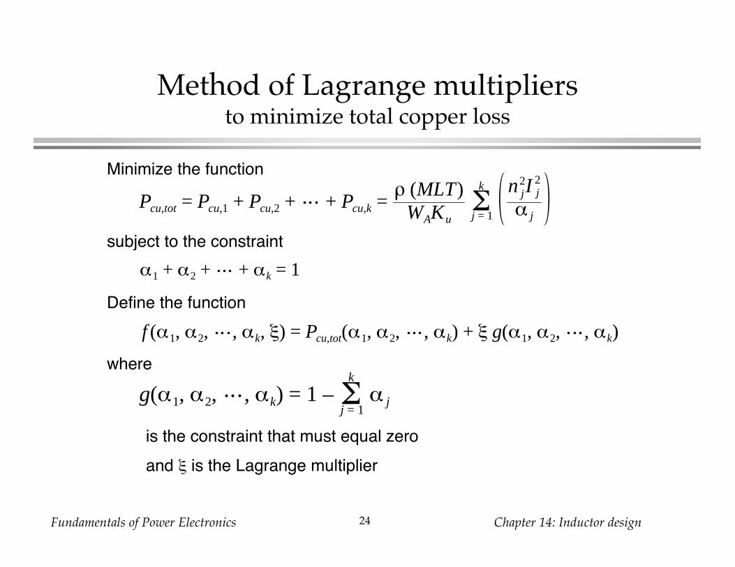
Method of Lagrange multipliersto minimize total copper loss
Pcu,tot = Pcu,1 + Pcu,2 + + Pcu,k =ρ (MLT)
WAKu
n j2I j
2
α jΣj = 1
k
subject to the constraint
α1 + α2 + + αk = 1
Define the function
f (α1, α2, , αk, ξ) = Pcu,tot(α1, α2, , αk) + ξ g(α1, α2, , αk)
Minimize the function
where
g(α1, α2, , αk) = 1 – α jΣj = 1
k
is the constraint that must equal zero
and is the Lagrange multiplier
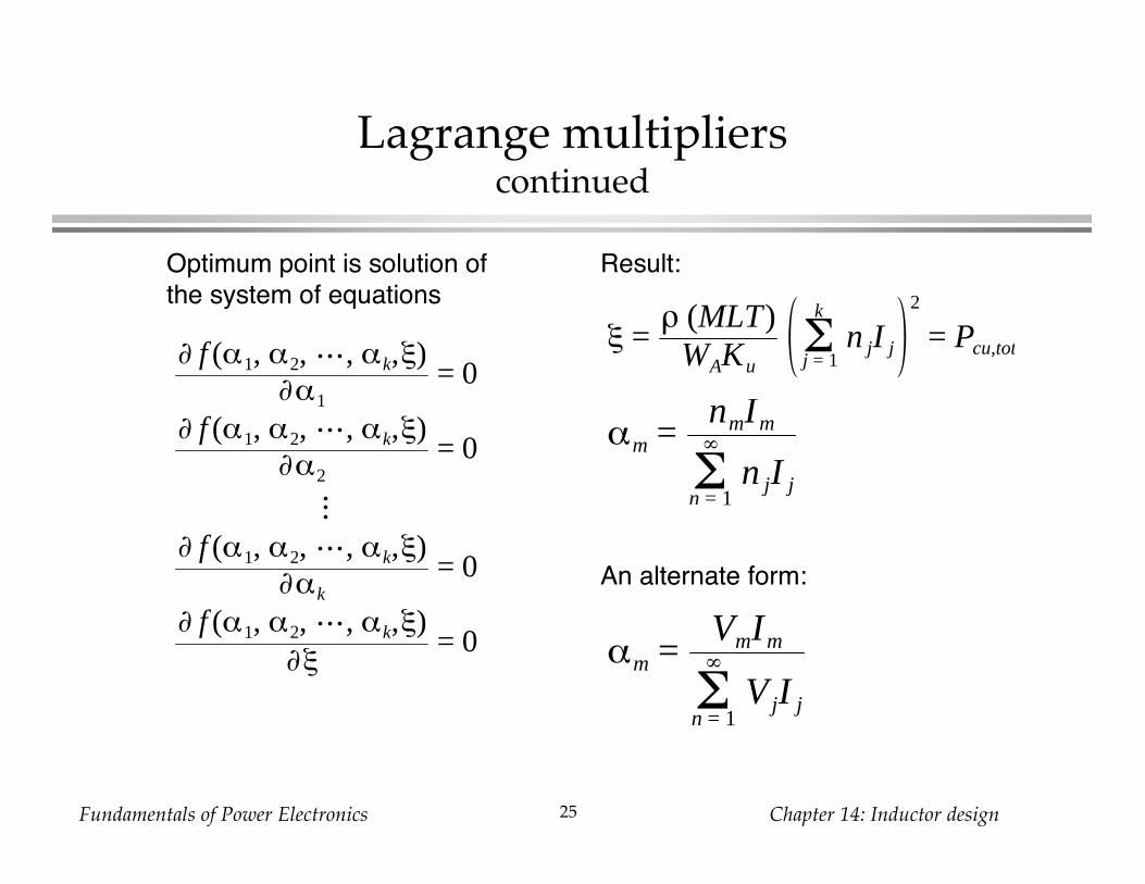
Fundamentals of Power Electronics Chapter 14: Inductor design25
Lagrange multiplierscontinued
Optimum point is solution of
the system of equations
∂ f (α1, α2, , αk,ξ)∂α1
= 0
∂ f (α1, α2, , αk,ξ)∂α2
= 0
∂ f (α1, α2, , αk,ξ)∂αk
= 0
∂ f (α1, α2, , αk,ξ)∂ξ
= 0
Result:
ξ =ρ (MLT)
WAKun jI jΣ
j = 1
k 2
= Pcu,tot
αm =nmIm
n jI jΣn = 1
∞
An alternate form:
αm =VmIm
VjI jΣn = 1
∞
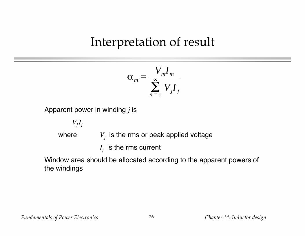
Fundamentals of Power Electronics Chapter 14: Inductor design26
Interpretation of result
αm =VmIm
VjI jΣn = 1
∞
Apparent power in winding j is
Vj Ij
where Vj is the rms or peak applied voltage
Ij is the rms current
Window area should be allocated according to the apparent powers of
the windings
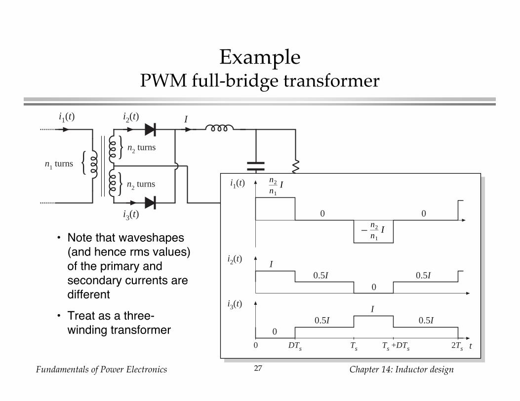
Fundamentals of Power Electronics Chapter 14: Inductor design27
Ii1(t)
n1 turns n2 turns
n2 turns
i2(t)
i3(t)
ExamplePWM full-bridge transformer
• Note that waveshapes
(and hence rms values)
of the primary and
secondary currents are
different
• Treat as a three-
winding transformer
– n2
n1I
t
i1(t)
0 0
n2
n1I
i2(t) I0.5I 0.5I
0
i3(t) I0.5I 0.5I
0
0 DTs Ts 2TsTs +DTs
Fundamentals of Power Electronics Chapter 14: Inductor design28
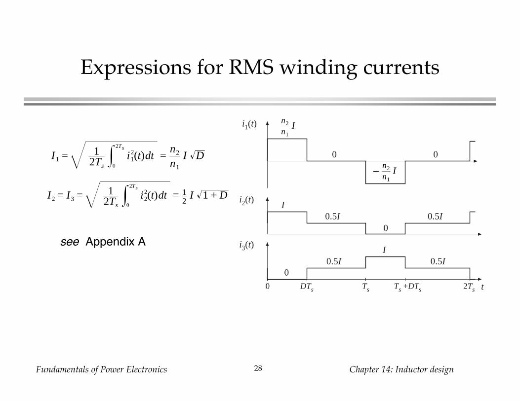
Expressions for RMS winding currents
I1 = 12Ts
i12(t)dt
0
2Ts
=n2
n1
I D
I2 = I3 = 12Ts
i22(t)dt
0
2Ts
= 12
I 1 + D
see Appendix A
– n2
n1I
t
i1(t)
0 0
n2
n1I
i2(t) I0.5I 0.5I
0
i3(t) I0.5I 0.5I
0
0 DTs Ts 2TsTs +DTs
Fundamentals of Power Electronics Chapter 14: Inductor design29
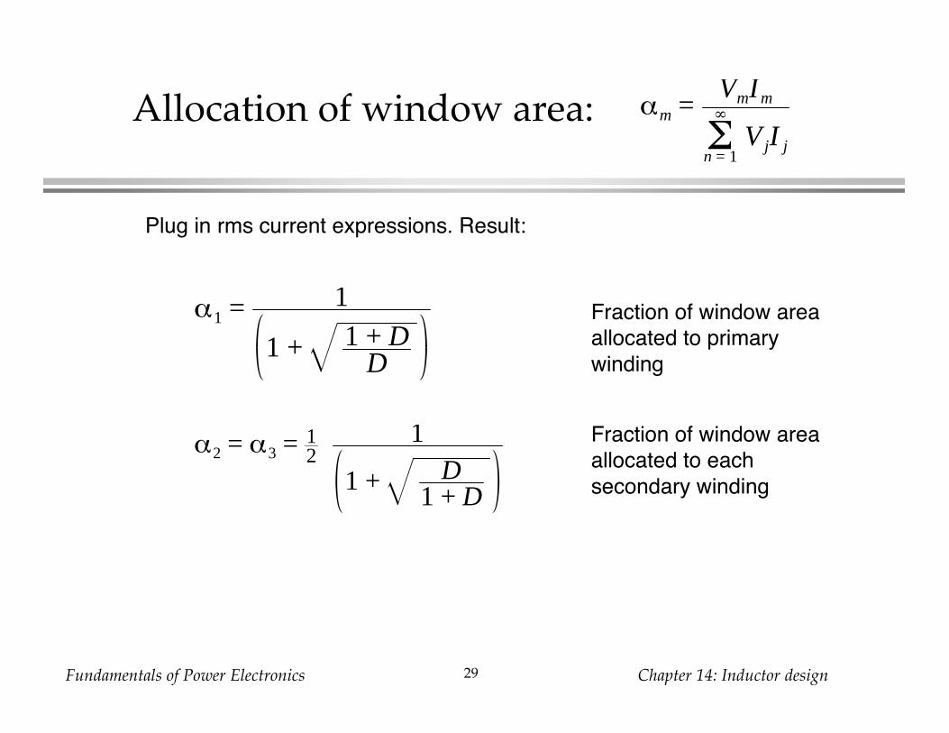
Allocation of window area: αm =VmIm
VjI jΣn = 1
∞
α1 = 1
1 + 1 + DD
α2 = α3 = 12
1
1 + D1 + D
Plug in rms current expressions. Result:
Fraction of window area
allocated to primary
winding
Fraction of window area
allocated to each
secondary winding

Fundamentals of Power Electronics Chapter 14: Inductor design30
Numerical example
Suppose that we decide to optimize the transformer design at theworst-case operating point D = 0.75. Then we obtain
α1 = 0.396α2 = 0.302α3 = 0.302
The total copper loss is then given by
Pcu,tot =ρ(MLT)
WAKun jI jΣ
j = 1
3 2
=ρ(MLT)n2
2I 2
WAKu1 + 2D + 2 D(1 + D)
Fundamentals of Power Electronics Chapter 14: Inductor design31
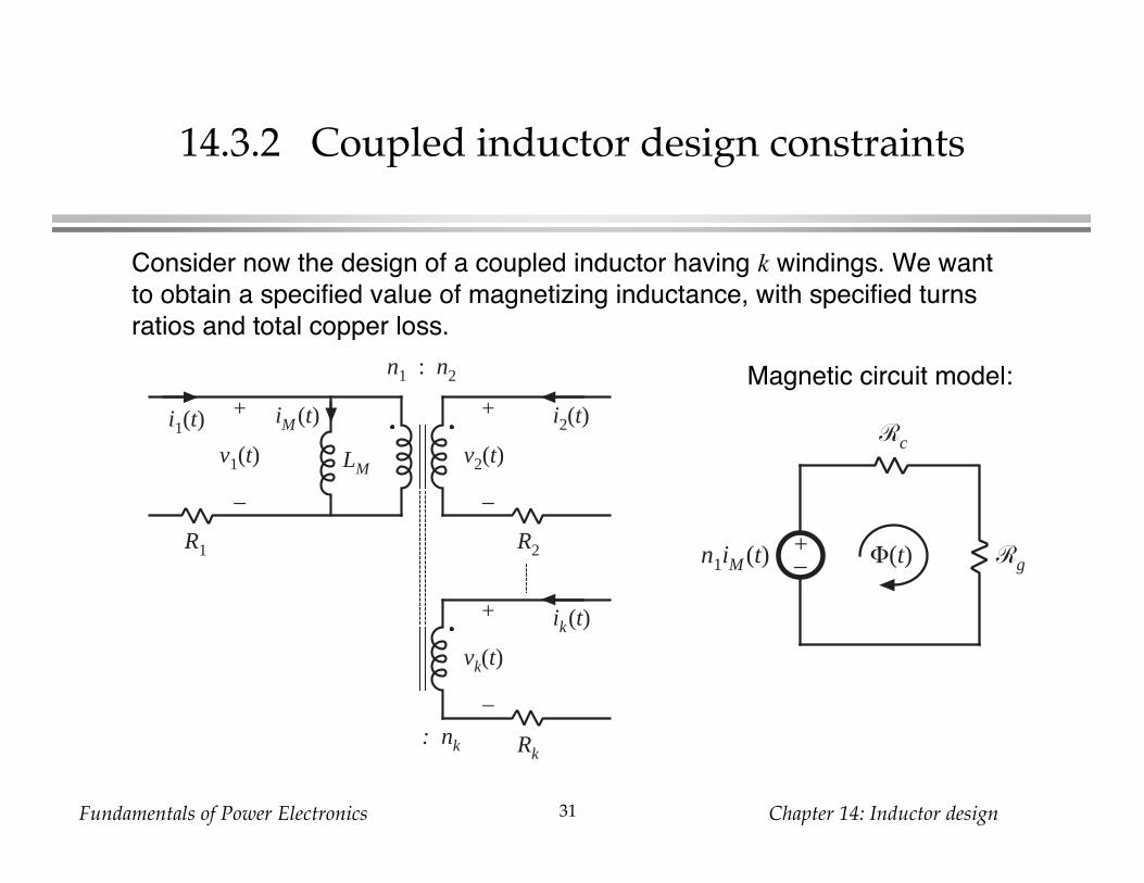
14.3.2 Coupled inductor design constraints
n1 : n2
: nk
R1 R2
Rk
+
v1(t)
–
+
v2(t)
–
+
vk(t)
–
i1(t) i2(t)
ik(t)
LM
iM (t)
+–n1iM (t) Φ(t)
Rc
Rg
Consider now the design of a coupled inductor having k windings. We want
to obtain a specified value of magnetizing inductance, with specified turns
ratios and total copper loss.
Magnetic circuit model:
Fundamentals of Power Electronics Chapter 14: Inductor design32
14.4 Examples
14.4.1 Coupled Inductor for a Two-Output Forward
Converter
14.4.2 CCM Flyback Transformer
Fundamentals of Power Electronics Chapter 14: Inductor design33
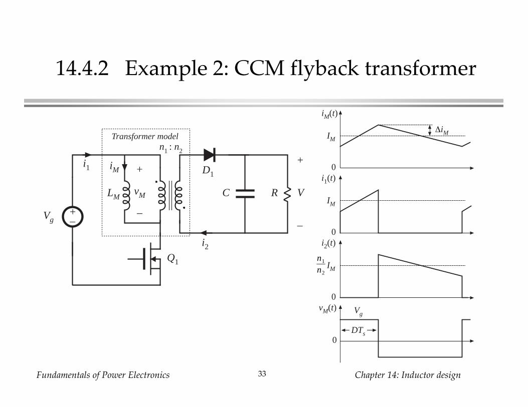
14.4.2 Example 2: CCM flyback transformer
+–
LM
+
V
–Vg
Q1
D1
n1 : n2
C
Transformer model
iMi1
R
+
vM
–
i2
vM(t)
0
Vg
DTs
iM(t)
IM
0
∆iM
i1(t)
IM
0i2(t)
IM
0
n1
n2

Fundamentals of Power Electronics Chapter 14: Inductor design34
Specifications
Input voltage Vg = 200V
Output (full load) 20 V at 5 A
Switching frequency 150 kHz
Magnetizing current ripple 20% of dc magnetizing current
Duty cycle D = 0.4
Turns ratio n2/n1 = 0.15
Copper loss 1.5 W
Fill factor Ku = 0.3
Maximum flux density Bmax = 0.25 T
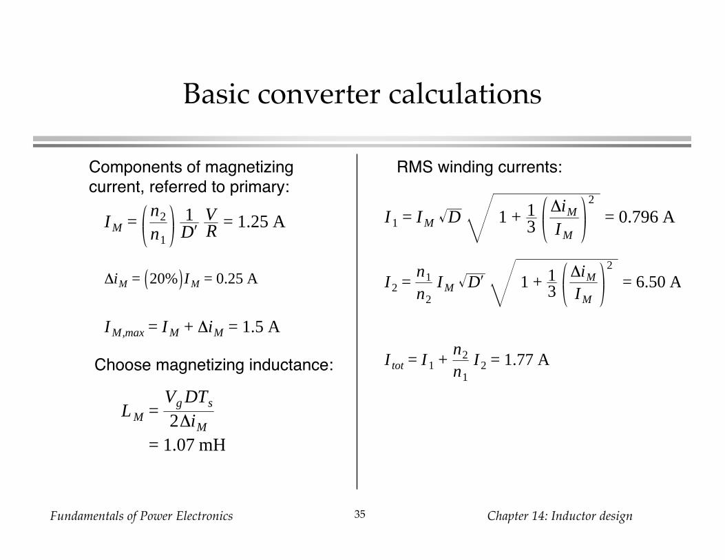
Fundamentals of Power Electronics Chapter 14: Inductor design35
Basic converter calculations
I M =n2
n1
1D′
VR = 1.25 A
∆iM = 20% I M = 0.25 A
I M,max = I M + ∆iM = 1.5 A
Components of magnetizing
current, referred to primary:
Choose magnetizing inductance:
L M =Vg DTs
2∆iM
= 1.07 mH
RMS winding currents:
I1 = I M D 1 + 13
∆iM
I M
2
= 0.796 A
I2 =n1
n2
I M D′ 1 + 13
∆iM
I M
2
= 6.50 A
I tot = I1 +n2
n1
I2 = 1.77 A
Fundamentals of Power Electronics Chapter 14: Inductor design36
Choose core size
Kg ≥ρLM
2 I tot2 I M,max
2
Bmax2 Pcu Ku
108
=1.724 ⋅ 10– 6Ω-cm 1.07 ⋅ 10– 3 H
21.77 A
21.5 A
2
0.25 T2
1.5 W 0.3108
= 0.049 cm5
The smallest EE core that satisfies this inequality (Appendix D) is the
EE30.
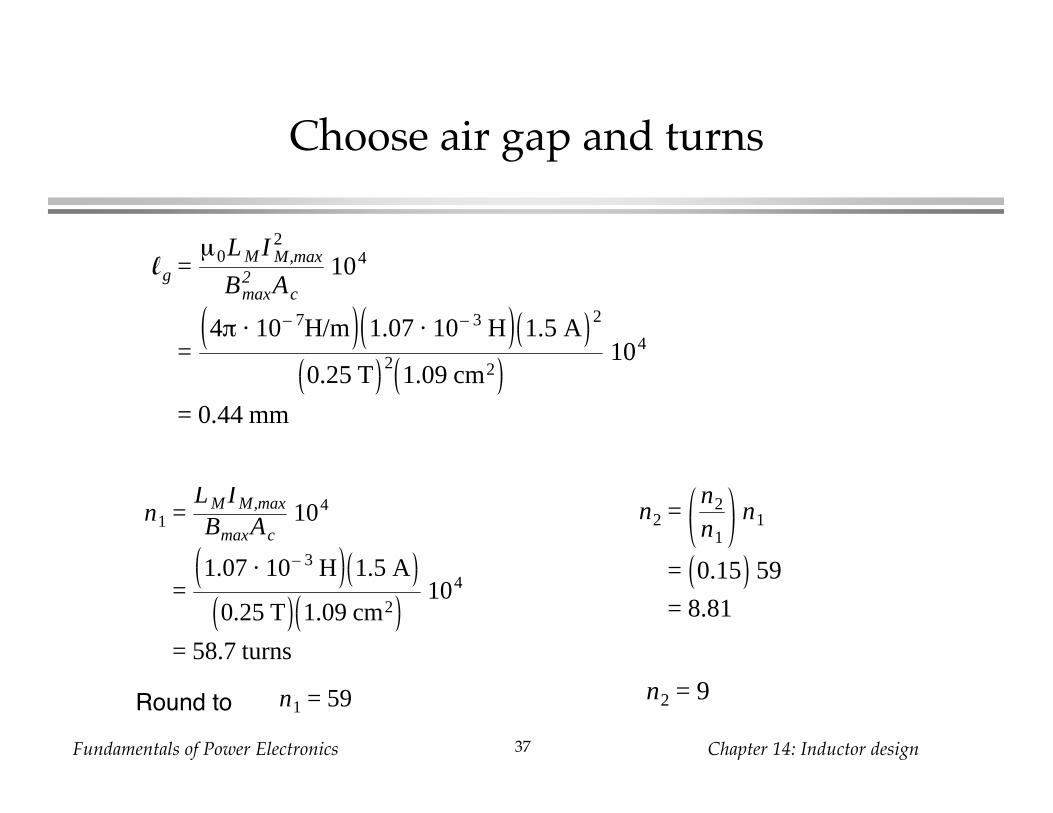
Fundamentals of Power Electronics Chapter 14: Inductor design37
Choose air gap and turns
lg =µ0L M I M,max
2
Bmax2 Ac
104
=4π ⋅ 10– 7H/m 1.07 ⋅ 10– 3 H 1.5 A
2
0.25 T2
1.09 cm2104
= 0.44 mm
n1 =L M I M,max
BmaxAc104
=1.07 ⋅ 10– 3 H 1.5 A
0.25 T 1.09 cm2104
= 58.7 turns
n1 = 59Round to
n2 =n2
n1
n1
= 0.15 59
= 8.81
n2 = 9
Fundamentals of Power Electronics Chapter 14: Inductor design38
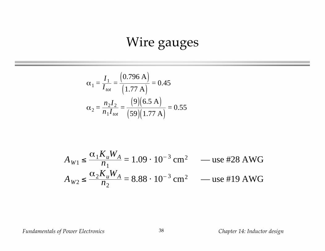
Wire gauges
α1 =I1I tot
=0.796 A
1.77 A= 0.45
α2 =n2I2n1I tot
=9 6.5 A
59 1.77 A= 0.55
AW1 ≤α1KuWA
n1= 1.09 ⋅ 10– 3 cm2 — use #28 AWG
AW2 ≤α2KuWA
n2= 8.88 ⋅ 10– 3 cm2 — use #19 AWG
Fundamentals of Power Electronics Chapter 14: Inductor design39
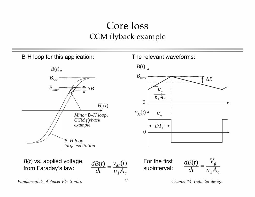
Core lossCCM flyback example
dB(t)dt
=vM (t)n1Ac
dB(t)dt
=Vg
n1Ac
B(t)
Hc(t)
Minor B–H loop,CCM flybackexample
B–H loop,large excitation
Bsat
∆BBmax
vM(t)
0
Vg
DTs
B(t)
Bmax
0
∆B
Vg
n1Ac
B-H loop for this application: The relevant waveforms:
B(t) vs. applied voltage,
from Faraday’s law:
For the first
subinterval:
Fundamentals of Power Electronics Chapter 14: Inductor design40
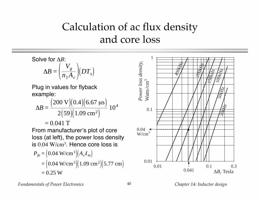
Calculation of ac flux densityand core loss
Solve for B:
∆B =Vg
n1AcDTs
Plug in values for flyback
example:
∆B =200 V 0.4 6.67 µs
2 59 1.09 cm2104
= 0.041 T
∆B, Tesla0.01 0.1 0.3
Pow
er lo
ss d
ensi
ty,
Wat
ts/c
m3
0.01
0.1
1
20kH
z50
kHz
100k
Hz
200k
Hz
400k
Hz
150k
Hz
0.04W/cm3
0.041
From manufacturer’s plot of core
loss (at left), the power loss density
is 0.04 W/cm3. Hence core loss is
Pfe = 0.04 W/cm3 Ac lm
= 0.04 W/cm3 1.09 cm2 5.77 cm
= 0.25 W
Fundamentals of Power Electronics Chapter 14: Inductor design41
Comparison of core and copper loss
• Copper loss is 1.5 W
– does not include proximity losses, which could substantially increase
total copper loss
• Core loss is 0.25 W
– Core loss is small because ripple and B are small
– It is not a bad approximation to ignore core losses for ferrite in CCM
filter inductors
– Could consider use of a less expensive core material having higher
core loss
– Neglecting core loss is a reasonable approximation for this
application
• Design is dominated by copper loss
– The dominant constraint on flux density is saturation of the core,
rather than core loss
Fundamentals of Power Electronics Chapter 14: Inductor design42
14.5 Summary of key points
1. A variety of magnetic devices are commonly used in switching
converters. These devices differ in their core flux density
variations, as well as in the magnitudes of the ac winding
currents. When the flux density variations are small, core loss can
be neglected. Alternatively, a low-frequency material can be used,
having higher saturation flux density.
2. The core geometrical constant Kg is a measure of the magnetic
size of a core, for applications in which copper loss is dominant.In the Kg design method, flux density and total copper loss are
specified.