Chapter 12 - ADC Testing
87
Chapter 12 - ADC Testing
-
Upload
monal-bhoyar -
Category
Documents
-
view
237 -
download
3
Transcript of Chapter 12 - ADC Testing

8/13/2019 Chapter 12 - ADC Testing
http://slidepdf.com/reader/full/chapter-12-adc-testing 1/87
Chapter 12 - ADC Testing
8/13/2019 Chapter 12 - ADC Testing
http://slidepdf.com/reader/full/chapter-12-adc-testing 2/87
8/13/2019 Chapter 12 - ADC Testing
http://slidepdf.com/reader/full/chapter-12-adc-testing 3/87
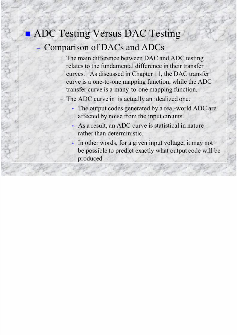
ADC Testing Versus DAC Testing
– Statistical Behavior of ADCs
– To understand the statistical nature of ADCs, we have to
model the ADC as a combination of a perfect ADC and a
noise source with no DC offset.
• The noise source represents the combination of the
noise portion of the real-world input signal plus the
self-generated noise of the ADCs input circuits.
Input
Signal
Noise
Source
Noise-
Free
ADC
8/13/2019 Chapter 12 - ADC Testing
http://slidepdf.com/reader/full/chapter-12-adc-testing 4/87
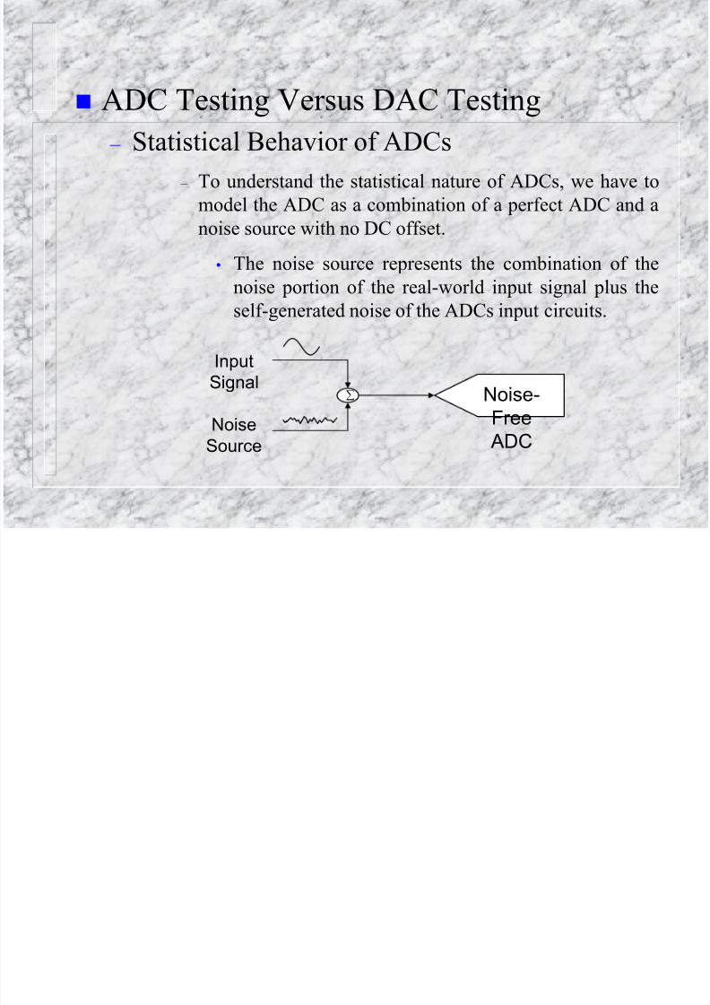
ADC Testing Versus DAC Testing
– Statistical Behavior of ADCs
– Applying a DC level to the noisy ADC, we can begin to
understand the statistical nature of ADC decision levels.
A noise-free ADC might be described by a simple
output/input relationship such as:
– Output code = Quantize( Input Voltage )
– where the function Quantize( ) represents the noise-free
ADC’s quantization process. The noisy ADC can be
described using a similar equation:
– Output code = Quantize ( Input Voltage + Noise Voltage )
8/13/2019 Chapter 12 - ADC Testing
http://slidepdf.com/reader/full/chapter-12-adc-testing 5/87
ADC Testing Versus DAC Testing
– Statistical Behavior of ADCs
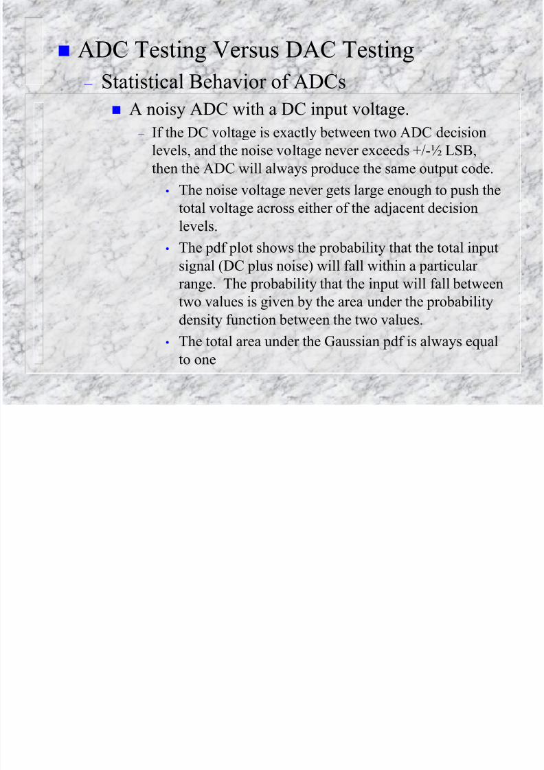
A noisy ADC with a DC input voltage.
– If the DC voltage is exactly between two ADC decision
levels, and the noise voltage never exceeds +/-½ LSB,
then the ADC will always produce the same output code.
• The noise voltage never gets large enough to push thetotal voltage across either of the adjacent decision
levels.
• The pdf plot shows the probability that the total input
signal (DC plus noise) will fall within a particular
range. The probability that the input will fall betweentwo values is given by the area under the probability
density function between the two values.
• The total area under the Gaussian pdf is always equal
to one
8/13/2019 Chapter 12 - ADC Testing
http://slidepdf.com/reader/full/chapter-12-adc-testing 6/87
Input Voltage
(DC Plus
Noise)
ADC
Decision
LevelsCode 1 Code 2
Input VoltageProbability
Average
Voltage
(DC Input)
Gaussian
Noise pdf

8/13/2019 Chapter 12 - ADC Testing
http://slidepdf.com/reader/full/chapter-12-adc-testing 7/87
ADC Testing Versus DAC Testing
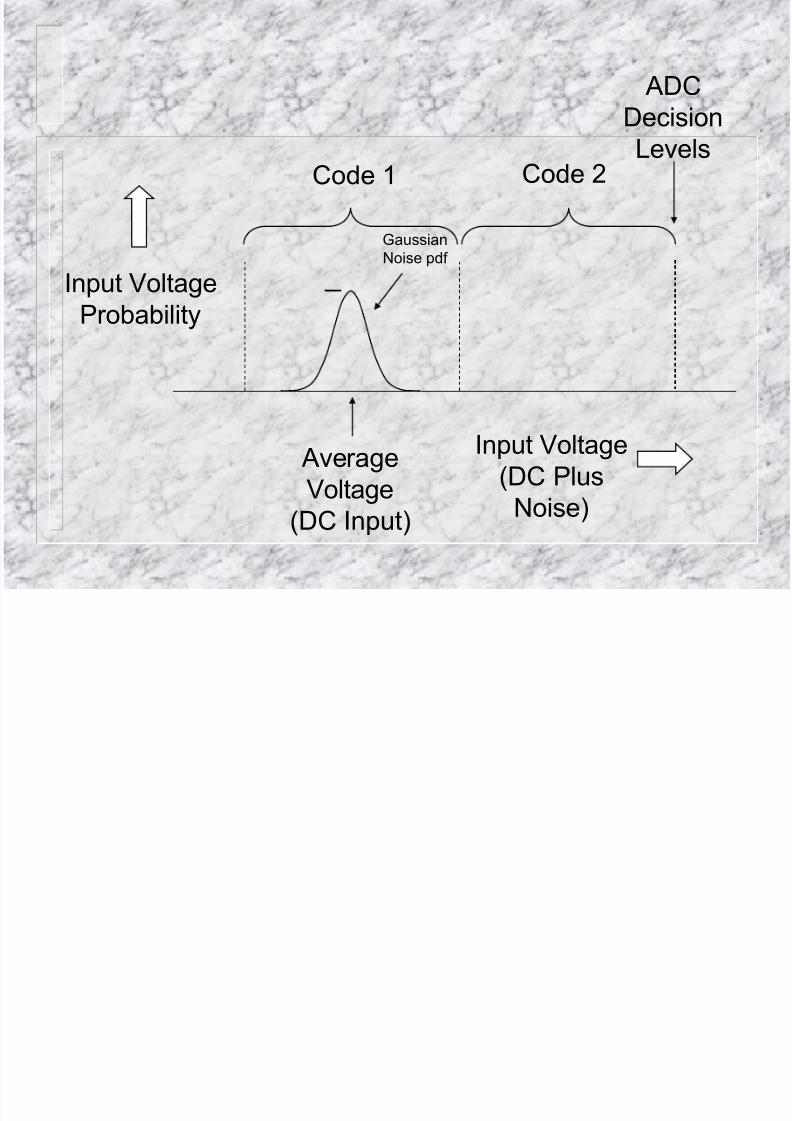
– Statistical Behavior of ADCs – On the other hand, if the DC input voltage is exactly equal
to a decision level, then even a tiny amount of noise
voltage will cause the quantization process to randomly
toggle between the two codes on either side of the decisionlevel.
– Assuming the statistical distribution of noise is
symmetrical, as in the case of the Gaussian pdf, the ADC
will produce an equal number of each of the two codes.
– The area under the pdf is equally split between code 1 andcode 2, so we would expect 50% of the ADC conversions
to produce code1 and 50% of the conversions to produce
code 2.
8/13/2019 Chapter 12 - ADC Testing
http://slidepdf.com/reader/full/chapter-12-adc-testing 8/87
Input
Voltage (DC
Plus Noise)
Code 1 Code 2
InputVoltage
Probability
50%Probability for
Code 1
50%Probability for
Code 2

8/13/2019 Chapter 12 - ADC Testing
http://slidepdf.com/reader/full/chapter-12-adc-testing 9/87
ADC Testing Versus DAC Testing
– Statistical Behavior of ADCs
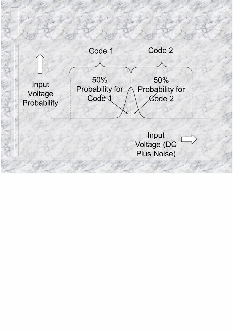
– For input voltages that are close but not equal to the
decision levels, the process gets more complicated.
• Consider an input voltage that is DV Volts below one
of the ADC’s decision levels.
• Any time the noise voltage exceeds DV, the ADC
quantizer will trip to the next highest value.
– The probability that the noise voltage will not exceed DV
and trip the quantizer into the next code is equal to the
area underneath the portion of the pdf that is less than theADC decision level.
– This area is equal to the integral from minus infinity to DV
of the probability density function of the noise.
8/13/2019 Chapter 12 - ADC Testing
http://slidepdf.com/reader/full/chapter-12-adc-testing 10/87
Input
Voltage (DC
Plus Noise)
Code 1 Code 2
InputVoltage
Probability
Area 1 =Probability
for Code 1
Area 2 =Probability
for Code 2
DV
8/13/2019 Chapter 12 - ADC Testing
http://slidepdf.com/reader/full/chapter-12-adc-testing 11/87
ADC Testing Versus DAC Testing
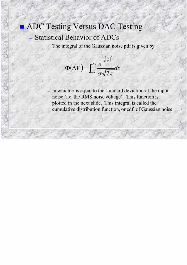
– Statistical Behavior of ADCs – The integral of the Gaussian noise pdf is given by
– in which s is equal to the standard deviation of the input
noise (i.e. the RMS noise voltage). This function is plotted in the next slide. This integral is called the
cumulative distribution function, or cdf, of Gaussian noise.
dxeV V
x
D
D s
s
2
2
2
1

8/13/2019 Chapter 12 - ADC Testing
http://slidepdf.com/reader/full/chapter-12-adc-testing 12/87
0.5
1
1.0s +1.0s
DV
DVV
Cumulative Distribution Function of Gaussian Noise

8/13/2019 Chapter 12 - ADC Testing
http://slidepdf.com/reader/full/chapter-12-adc-testing 13/87
-3.0 -2.9 -2.8 -2.7 -2.6 -2.5 -2.4 -2.3 -2.2 -2.1
0.0013 0.0019 0.0026 0.0035 0.0047 0.0062 0.0082 0.0107 0.0139 0.0179
-2.0 -1.9 -1.8 -1.7 -1.6 -1.5 -1.4 -1.3 -1.2 -1.1
0.0228 0.0287 0.0359 0.0446 0.0548 0.0668 0.0808 0.0968 0.1151 0.1357
-1.0 -0.9 -0.8 -0.7 -0.6 -0.5 -0.4 -0.3 -0.2 -0.1
0.1587 0.1841 0.2119 0.2420 0.2743 0.3085 0.3446 0.3821 0.4207 0.4602
0.0 0.1 0.2 0.3 0.4 0.5 0.6 0.7 0.8 0.9
0.5000 0.5398 0.5793 0.6179 0.6554 0.6915 0.7257 0.7580 0.7881 0.8159
1.0 1.1 1.2 1.3 1.4 1.5 1.6 1.7 1.8 1.9
0.8413 0.8643 0.8849 0.9032 0.9192 0.9332 0.9452 0.9554 0.9641 0.9713
2.0 2.1 2.2 2.3 2.4 2.5 2.6 2.7 2.8 2.9
0.9772 0.9821 0.9861 0.9893 0.9918 0.9938 0.9953 0.9965 0.9974 0.9981
Gaussian Cumulative Distribution Function (cdf) Values

8/13/2019 Chapter 12 - ADC Testing
http://slidepdf.com/reader/full/chapter-12-adc-testing 14/87
Problem
– An ADC input is set to 2.453 VDC. The noise of the
ADC and DC signal source is characterized to be 10 mV
RMS and is assumed to be perfectly Gaussian. The
transition between code 134 and 135 occurs at 2.461 VDC
for this particular ADC, therefore the value 134 is the
expected output from the ADC with a DC input of2.453V. What is the probability that the ADC will
produce code 135 instead of 134? If we collected 200
samples from the output of the ADC, how many would we
expect to be 134 and how many would be 135? How
might we determine that the transition between code 134and 135 occurs at 2.461 VDC? How might we
characterize the effective RMS input noise?

8/13/2019 Chapter 12 - ADC Testing
http://slidepdf.com/reader/full/chapter-12-adc-testing 15/87
Solution:
– With an input of 2.453 VDC, the ADC’s input noise
would have to exceed (2.461 V – 2.453 V) = +8 mV to
cause the ADC to trip to code 135. This value is equal to
+0.8s, since s = 10 mV. From the table, the Gaussian
cdf of +0.8s is equal to 0.7881. Therefore, there is a
78.81% probability that the noise will not be sufficient to
trip the ADC to code 135. Thus, 78.81% of the time we
can expect code 134 and 21.19% of the time we canexpect code 135. If we collect 200 samples from the
ADC, we would expect 78.81% of the 200 samples
(approximately 158 samples) to be code 134. We would
expect the remaining 21.19% of the samples (42 samples)
to be code 135. – To determine the transition voltage, we simply have to
adjust the input voltage up or down until 50% of the
samples are equal to 134 and 50% are equal to 135. To
determine the value of s, we can adjust the input voltage
until we get 84.13% of the samples to equal 134.

8/13/2019 Chapter 12 - ADC Testing
http://slidepdf.com/reader/full/chapter-12-adc-testing 16/87
ADC Testing Versus DAC Testing
– Statistical Behavior of ADCs – Because an ADC’s circuits generate random noise, the
ADC decision levels represent probable locations of
transitions from one code to the next.
– If we plot the average output code from a typical ADC
versus DC input levels, we will see the true transfer
characteristics of the ADC.
– The center of the transition from one code to the next (i.e.
the decision level) is often called a code edge.
• The wider the distribution of the Gaussian input noise,
the more rounded the transitions from one code to thenext will be.
• In fact, the true ADC transfer characteristic is equal to
the convolution of the Gaussian noise probability
density function with the noise-free transfer curve
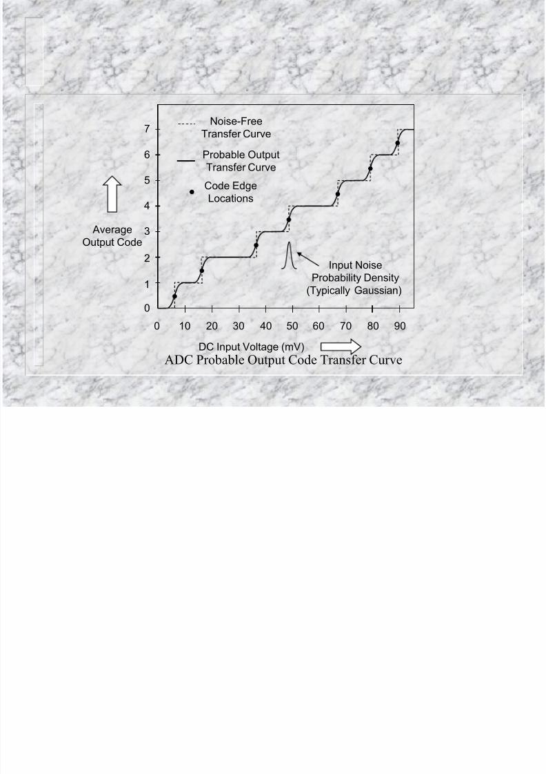
8/13/2019 Chapter 12 - ADC Testing
http://slidepdf.com/reader/full/chapter-12-adc-testing 17/87
Average
Output Code
0
1
2
3
4
5
6
7
DC Input Voltage (mV)
0 10 20 4030 50 60 70 80 90
Input Noise
Probability Density
(Typically Gaussian)
Noise-Free
Transfer Curve
Probable Output
Transfer Curve
Code Edge
Locations
ADC Probable Output Code Transfer Curve

8/13/2019 Chapter 12 - ADC Testing
http://slidepdf.com/reader/full/chapter-12-adc-testing 18/87
ADC Testing Versus DAC Testing
– Statistical Behavior of ADCs – Code edge measurement is one of the primary differences
between ADC and DAC testing.
– DAC voltages can simply be measured one at a time using
a DC voltmeter or digitizer.
– Exact ADC code edges can only be measured using an
iterative process in which the input voltage is adjusted
until the output samples toggles equally between two
codes.
– Because of the statistical nature of the ADC’s transfer
curve, each iteration of the search requires 100 or more
conversions to achieve a repeatable average value. Since
this brute-force approach would lead to very long test
times in production, a number of faster methodologies
have been developed.
8/13/2019 Chapter 12 - ADC Testing
http://slidepdf.com/reader/full/chapter-12-adc-testing 19/87
8/13/2019 Chapter 12 - ADC Testing
http://slidepdf.com/reader/full/chapter-12-adc-testing 20/87
Average
Output
Code
0
1
2
3
4
5
6
7
DC Input Voltage (mV)
0 10 20 4030 50 60 70 80 90
Code Edge
Locations
Code Edge
Locations
Code Center
Locations
Code Center
Locations
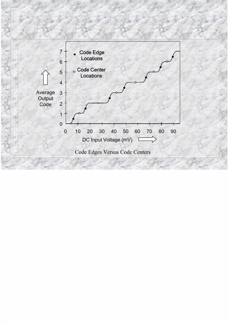
Code Edges Versus Code Centers

8/13/2019 Chapter 12 - ADC Testing
http://slidepdf.com/reader/full/chapter-12-adc-testing 21/87
ADC Code Edge Measurements
– Edge Code Testing versus Center Code Testing
– Notice that the code centers fall very nearly on a straight
line while the code edges show a much less linear transfer
curve. The averaging process in the definition of code
centers produces an artificially low DNL result compared
to edge code testing. Because the code widths alternate
between wide and narrow codes, the averaging process
effectively smoothes these variations out, leaving a
transfer characteristic that looks like it has fairly evenly
spaced steps.
– Because center code testing produces an artificially low
DNL value, this technique is not preferred. The edge code
method is a more discerning test, and is therefore the
preferred means of translating the transfer curve of an
ADC to the one-to-one mapping needed for INL and DNL
measurements.

8/13/2019 Chapter 12 - ADC Testing
http://slidepdf.com/reader/full/chapter-12-adc-testing 22/87
ADC Code Edge Measurements
– Step Search and Binary Search Methods – The most obvious method to find the edge between two
ADC codes is to simply adjust the input voltage of the
ADC up or down until the output codes are evenly divided
between the first code and the second. To achieverepeatable results, we need to collect about 50 to 100
samples from the ADC so that we have a statistically
significant number of conversions. The input voltage
adjustment could be performed using a simple step search,
but a faster method is to use a binary search to quickly
find the input voltage corresponding to the ADC code
edge.

8/13/2019 Chapter 12 - ADC Testing
http://slidepdf.com/reader/full/chapter-12-adc-testing 23/87
ADC Code Edge Measurements
– Step Search and Binary Search Methods
– Binary searches are an acceptable production test method
for comparators and slicer circuits, which are effectively
one-bit ADCs. However, if we try to apply a binary
search technique to multi-bit ADCs in production, we run
into a major problem. If we use a binary search with, say,
five iterations, we have to collect 100 samples for eachiteration. This would result in a total of 500 collected
samples per code edge. An N-bit ADC has 2 N-1 code
edges. Therefore, the test time for most ADCs would be
far too high.
• For example, a 10-bit ADC operating at a sampling
rate of 100 kHz would require a total data collection
time of 500 codes times 210-1 edges times the sample
period (1/100 kHz). Thus the total collection time
would be 500 x 1023 x 10 us = 5.115 seconds!

8/13/2019 Chapter 12 - ADC Testing
http://slidepdf.com/reader/full/chapter-12-adc-testing 24/87
ADC Code Edge Measurements
– Servo Method
– A much better method for measuring code edges in
production is the use of a servo circuit. The following is a
simplified block diagram of an ADC servo measurement
setup.
– The output codes from the ADC are compared against a
value programmed into the search register. If the ADC
output is greater than or equal to the expected value, the
integrator ramps downward. If it is less than the expected
value, the integrator ramps upward. Eventually, the
integrator finds the desired code edge and fluctuates back
and forth across the transition level. The average (low
pass filtered) voltage at the ADC input represents the
lower edge of the code under test. This voltage can easily
be measured using a DC voltmeter. The process is
repeated for each code edge in the ADC transfer curve.
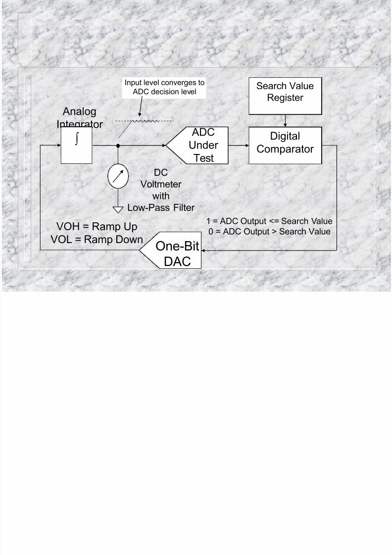
8/13/2019 Chapter 12 - ADC Testing
http://slidepdf.com/reader/full/chapter-12-adc-testing 25/87
DigitalComparator
Analog
Integrator ADC
Under
Test
Search Value
Register
DC
Voltmeter
with
Low-Pass Filter1 = ADC Output <= Search Value
0 = ADC Output > Search Value
One-Bit
DAC
VOH = Ramp Up
VOL = Ramp Down
Input level converges to
ADC decision level
8/13/2019 Chapter 12 - ADC Testing
http://slidepdf.com/reader/full/chapter-12-adc-testing 26/87
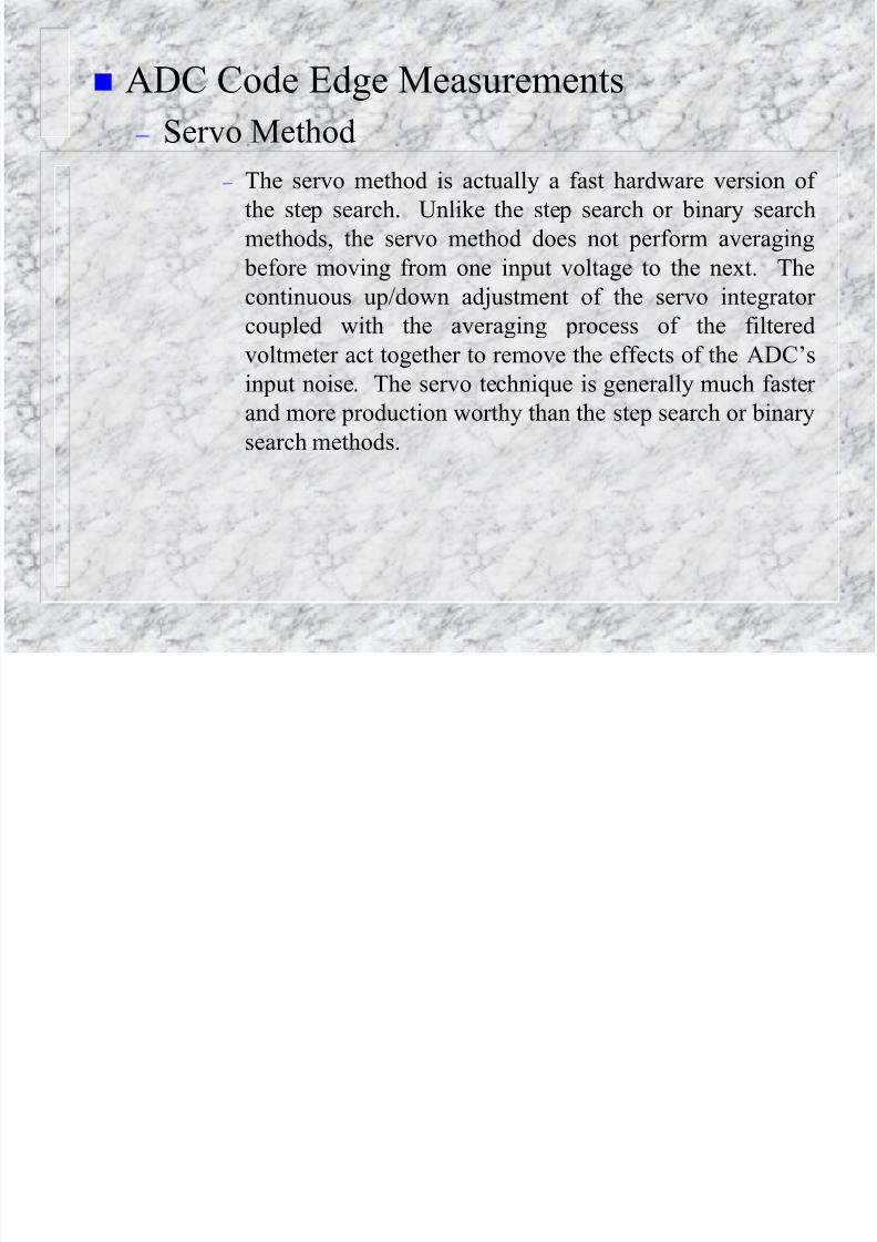
ADC Code Edge Measurements
– Servo Method
– The servo method is actually a fast hardware version of
the step search. Unlike the step search or binary search
methods, the servo method does not perform averaging
before moving from one input voltage to the next. The
continuous up/down adjustment of the servo integrator
coupled with the averaging process of the filtered
voltmeter act together to remove the effects of the ADC’s
input noise. The servo technique is generally much faster
and more production worthy than the step search or binary
search methods.
8/13/2019 Chapter 12 - ADC Testing
http://slidepdf.com/reader/full/chapter-12-adc-testing 27/87
ADC Code Edge Measurements
– Linear Ramp Histogram Method
– Servo method is faster than the binary search method, yet
it is fairly slow compared with the more common
production histogram testing technique. Histogram
testing requires an input signal with a known voltage
distribution, such as a linear ramp; two commonly used
histogram methods: linear ramp and sinusoidal method.
– The simplest way to perform a histogram test is to apply a
rising or falling linear ramp to the input of the ADC and
collect samples from the ADC at a constant sampling rate.
The ADC samples are captured as the input ramp slowly
moves from one end of the ADC conversion range to the
other. The ramp is set to rise or fall slowly enough that
each ADC code is “hit” several times. The number of
occurrences of each code is directly proportional to the
width of the code. In other words, wide codes are hit more
often than narrow codes

8/13/2019 Chapter 12 - ADC Testing
http://slidepdf.com/reader/full/chapter-12-adc-testing 28/87
ADC Code Edge Measurements
– Linear Ramp Histogram Method – For example, if the voltage spacing between the upper and
lower decision levels for code 2 are twice as wide as the
spacing for code 1, then we expect code 2 to occur twice
as often as code 1. The reason for this is that it takes thelinear ramp input signal twice as long to sweep through
code 2 as it takes to sweep through code 1. Of course, this
method assumes that the ramp is perfectly linear and that
the ADC sampling rate is constant throughout the entire
ramp

8/13/2019 Chapter 12 - ADC Testing
http://slidepdf.com/reader/full/chapter-12-adc-testing 29/87
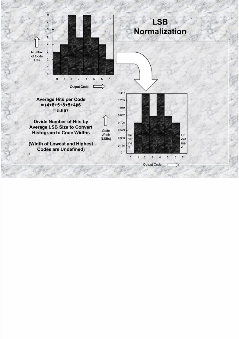
– The number of occurrences of each code is plotted as a
histogram. Ideally, each code should be hit the same
number of times, but this would only be true for a
perfectly linear ADC. The picture shows us which codes
are hit more often, indicating that they are wider codes.For example, we can see from the histogram in that codes
2 and 4 are twice as wide as codes 1 and 6.
Output Code
0
1
2
3
4
5
6
7
Input Voltage (mV)
0 10 20 4030 50 60 70 80 90
ADC Samples
8/13/2019 Chapter 12 - ADC Testing
http://slidepdf.com/reader/full/chapter-12-adc-testing 30/87
Number
of Code
Hits
0
1
2
3
4
5
6
7
Output Code
0 1 2 43 5 6 7
8
Code
Width
(LSBs)
0
0.176
0.353
0.529
0.706
0.882
1.059
1.235
0 1 2 43 5 6 7
1.412
0
1
2
3
4
5
6
7
Output Code
0 1 2 43 5 6 7
8
Un
def
ine
d
Un
def
ine
d
Average Hits per Code
= (4+8+5+8+5+4)/6
= 5.667
Divide Number of Hits by
Average LSB Size to ConvertHistogram to Code Widths
(Width of Lowest and Highest
Codes are Undefined)12
Output Code
LSB
Normalization

8/13/2019 Chapter 12 - ADC Testing
http://slidepdf.com/reader/full/chapter-12-adc-testing 31/87
ADC Code Edge Measurements
– Linear Ramp Histogram Method
– Dividing the histogram by the average number of hits for
each code normalizes the plot so that it represents ADC
code widths in LSBs.
– We can subtract one from each value in this plot to
calculate the ADC’s endpoint DNL curve. The DNLcurve can then be integrated using a running sum to
calculate the endpoint INL curve.
– Notice that the number of hits for the lowest and highest
codes is meaningless, since these two codes do not have a
defined code width. In effect, the end codes are infinitelywide. For example, code 0 in an unsigned binary ADC
has no lower decision level, since there is no such code as
-1. These meaningless hits are ignored in the linear ramp
histogram analysis.

8/13/2019 Chapter 12 - ADC Testing
http://slidepdf.com/reader/full/chapter-12-adc-testing 32/87
ADC Code Edge Measurements
– Conversion from Histograms to Code Edge
Transfer Curves
– To calculate absolute or best-fit INL and DNL curves, we
have to determine the absolute voltage for each decision
level. Unfortunately, an LSB code width plot tells us the
width of each code in LSBs rather than Volts. To convertthe code width plot into voltage units, we need to measure
the average LSB size of the ADC, in Volts. This can be
done using a binary search or servo method to find the
lowest and highest code edge voltages, V+fs and - V-fs. In
an N-bit ADC, there are 2 N
-2 LSBs between these twocode edges. Therefore, the average LSB size can be
calculated as follows:
22)(
+
N
FS FS V V VoltseWidth AverageCod

8/13/2019 Chapter 12 - ADC Testing
http://slidepdf.com/reader/full/chapter-12-adc-testing 33/87
Problem
– A binary search method is used to find the transition
between code 0 and code 1 in the previous ADC graph.
The code edge is found to be 53 mV. A second binary
search determines the code edge between codes 6 and 7 to
be 2.77 V. What is the average LSB size for this 3-bit
ADC? Based on the previous histogram, what is the width
of each of the 8 codes, in Volts?

8/13/2019 Chapter 12 - ADC Testing
http://slidepdf.com/reader/full/chapter-12-adc-testing 34/87
Solution
– The average LSB size is equal to ( 2.77 V - 53 mV) / 23-2,or 452.8 mV. Therefore, the code width for each code is:
• Code 0: Undefined (infinite width)
• Code 1: 0.706 LSBs x 452.8 mV = 319.68 mV
• Code 2: 1.412 LSBs x 452.8 mV = 639.35 mV• Code 3: 0.882 LSBs x 452.8 mV = 399.37 mV
• Code 4: 1.412 LSBs x 452.8 mV = 639.35 mV
• Code 5: 0.882 LSBs x 452.8 mV = 399.37 mV
• Code 6: 0.706 LSBs x 452.8 mV = 319.68 mV
• Code 7: Undefined (infinite width)
8/13/2019 Chapter 12 - ADC Testing
http://slidepdf.com/reader/full/chapter-12-adc-testing 35/87
ADC Code Edge Measurements
– Conversion from Histograms to Code Edge
Transfer Curves
– If we wish to calculate the absolute voltage level of each
code edge, we simply perform a running sum on the code
widths, starting with the voltage V-FS. The resulting code
edge transfer curve is equivalent to a DAC output transfercurve, except that it will only have 2 N-1 values rather than
2 N values.
– Once we know the width of each code in Volts, and we
know the location of the first transition, in Volts, we can
easily reconstruct the ADC transfer curve. We simplycalculate a running sum of all the code widths, starting
with the first code edge.

8/13/2019 Chapter 12 - ADC Testing
http://slidepdf.com/reader/full/chapter-12-adc-testing 36/87
Problem
– Using the results of the previous problem, reconstruct the 3-bitADC transfer curve for each decision level.
Solution: – The transition from Code 0 to code 1 was measured using a
binary search. It was 53 mV. The other codes edges can becalculated using a running sum:
• Code 0 to Code 1: 53 mV
• Code 1 to Code 2: 53 mV + 319.68 mV = 372.68 mV
•
Code 2 to Code 3: 372.68 mV + 639.35 mV = 959.03 mV• Code 3 to Code 4: 959.03 mV + 399.37 mV = 1358.4 mV
• Code 4 to Code 5: 1358.4 mV + 639.35 mV = 1997.75 mV
• Code 5 to Code 6: 1997.75 mV + 399.37 mV = 2397.12 mV
• Code 6 to Code 7: 2397.12 mV + 319.68 mV = 2716.8 mV

8/13/2019 Chapter 12 - ADC Testing
http://slidepdf.com/reader/full/chapter-12-adc-testing 37/87
ADC Code Edge Measurements
– Accuracy Limitations of Histogram Testing
– Notice that we have an error in Example 12-3. The
histogram method measured the code edge between code 6
and 7 to be 2.717 V, yet our binary search found the edge
to be 2.77 V. The error is caused by the fact that we onlymeasured an average of 5 hits per code, giving us only 1/5
of an LSB of resolution. 1/5 of a 452.8 mV LSB
corresponds to a possible error of +/- 90.5 mV. The
problem is that we did not collect enough samples of each
ADC code in this simple example.
8/13/2019 Chapter 12 - ADC Testing
http://slidepdf.com/reader/full/chapter-12-adc-testing 38/87
ADC Code Edge Measurements
– Accuracy Limitations of Histogram Testing
– For characterization of the ADC, we would prefer to ramp
the input very slowly, so that each code is hit hundreds of
times instead of just 5 or 6 times. This would result in
better measurement resolution and repeatability, since the
input voltage steps would be spaced much closer together.
– Also, the random nature of the ADC decision levels would
be averaged out by the large sample size.
– In production testing, we can only afford to collect a
relatively small number of samples from each code,
typically 16 or 32. Otherwise the test time becomesexcessive.
– Therefore, even a perfect ADC will not produce a flat
histogram in production testing because the limited
number of samples collected gives rise to a limited code
width resolution and repeatability

8/13/2019 Chapter 12 - ADC Testing
http://slidepdf.com/reader/full/chapter-12-adc-testing 39/87
ADC Code Edge Measurements
– Accuracy Limitations of Histogram Testing – In addition to the accuracy limitation caused by limited
resolution, we have the additional problem of
repeatability. If we look carefully, we notice that several
of the codes occur so close to a decision level that the
ADC noise will cause the results to vary from one test
execution to the next even if our input signal is exactly the same during each test execution.
Output
Code
0
1
2
3
4
5
6
7
Input Voltage (mV)
0 10 20 4030 50 60 70 80 90
Consistent ADC
Samples
ADC Samples
with Uncertainty
Caused by Noise
Possible
Transition
Sequence
8/13/2019 Chapter 12 - ADC Testing
http://slidepdf.com/reader/full/chapter-12-adc-testing 40/87
ADC Code Edge Measurements
– Accuracy Limitations of Histogram Testing – In many cases, we find that the raw data sequence from
the ADC may zigzag up and down as the output codes
near a transition from one code to the next.
• For instance, it is possible to achieve an ADC output
sequence 4, 4, 4, 4, 4, 5, 4, 5, 5, 5 rather than the ideal
sequence 4, 4, 4, 4, 4, 4, 5, 5, 5, 5.
– Unfortunately, this is the nature of histogram testing of
ADCs. The results will be variable and somewhat
unrepeatable unless we collect many samples per code.
• In histogram testing, as in many other tests, there is an
inherent tradeoff between good repeatability and lowtest time.
– It is the test engineer’s responsibility to balance the need
for low test time with the need for acceptable accuracy and
repeatability.

8/13/2019 Chapter 12 - ADC Testing
http://slidepdf.com/reader/full/chapter-12-adc-testing 41/87
ADC Code Edge Measurements
– Rising Ramp versus Falling Ramp – Most ADC architectures include one or more analog
comparators in their design. Since comparators are
subject to hysteresis, it is not uncommon to find a
discrepancy between code edges measured using a rising
ramp and code edges measured using a falling ramp. The
most complete way to test and ADC is to test parameterssuch as INL and DNL using both a rising ramp and a
falling ramp. Both methods must produce a passing result
before the ADC is considered good. However, the extra
test doubles the test time, so we prefer to use only one
ramp. – If characterization shows that either the rising ramp or
falling ramp always produces the worst-case results, then
we can use only the worst-case test condition to save test
time.

8/13/2019 Chapter 12 - ADC Testing
http://slidepdf.com/reader/full/chapter-12-adc-testing 42/87
ADC Code Edge Measurements
– Rising Ramp versus Falling Ramp
– A compromise solution is to ramp the signal up at twice
the normal rate and then ramp it down again. This triangle
waveform approach tests both the falling and rising edge
locations, averaging their results.
– It takes no longer than a single ramp technique, but it
cancels the effects of hysteresis.
– A separate test should be performed to verify that the
ADC’s hysteresis errors are within acceptable limits. Thehysteresis test could be performed at only a few codes,
saving test time compared to the two-pass ramp solution.
8/13/2019 Chapter 12 - ADC Testing
http://slidepdf.com/reader/full/chapter-12-adc-testing 43/87
ADC Code Edge Measurements
– Sinusoidal Histogram Method
– Sinusoidal histogram tests were originally used to
compensate for the relatively poor linearity of early AWG
instruments.
• It is easier to produce a pure sinusoidal waveform
than to produce a perfectly linear ramp.
• A more common reason to use the sinusoidal
histogram method is that it allows better
characterization of the dynamic performance of the
ADC. The linear histogram technique is basically a
static performance test. Sometimes we need to test theADC transition levels in a more dynamic, real-world
situation. To do this, we can use a high frequency
sinusoidal input signal so the ADC responds to a
rapidly changing input of a sinusoid rather than the
slowly varying voltages of a ramp.

8/13/2019 Chapter 12 - ADC Testing
http://slidepdf.com/reader/full/chapter-12-adc-testing 44/87
ADC Code Edge Measurements
– Sinusoidal Histogram Method
– Ramp inputs have an even distribution of voltages over the
entire ADC input range. Sinusoids, on the other hand,
have an uneven distribution of voltages. A sine wave
spends much more time near the upper and lower peakthan at the center. As a result, we would expect to get
more code hits at the upper and lower codes than at the
center of the ADC’s transfer curve, even when testing a
perfect ADC. Fortunately, the distribution of voltage
levels in a pure sinusoid is well defined, so we cancompensate for the uneven distribution of voltages
inherent to sinusoidal waveforms.
8/13/2019 Chapter 12 - ADC Testing
http://slidepdf.com/reader/full/chapter-12-adc-testing 45/87
ADC Code Edge Measurements
– Sinusoidal Histogram Method
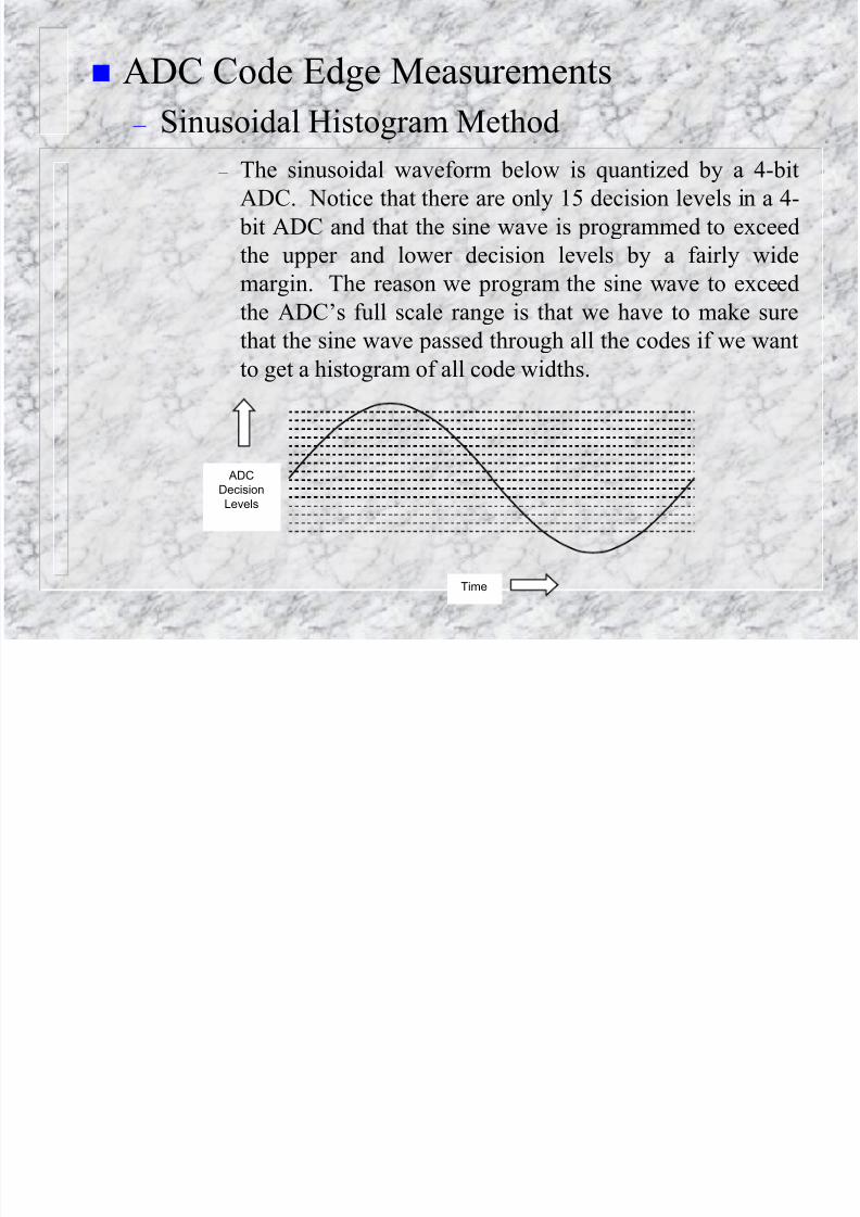
– The sinusoidal waveform below is quantized by a 4-bit
ADC. Notice that there are only 15 decision levels in a 4-
bit ADC and that the sine wave is programmed to exceed
the upper and lower decision levels by a fairly wide
margin. The reason we program the sine wave to exceed
the ADC’s full scale range is that we have to make surethat the sine wave passed through all the codes if we want
to get a histogram of all code widths.
Time
ADC
Decision
Levels

8/13/2019 Chapter 12 - ADC Testing
http://slidepdf.com/reader/full/chapter-12-adc-testing 46/87
ADC Code Edge Measurements
– Sinusoidal Histogram Method
– Clearly we get more code hits near the peaks of the sine
wave than at the center, even for this simple example. The
sinusoidal histogram of a perfect ADC appears as a
“bathtub” shape. Clearly, we need to normalize our
histogram to remove the effects of the sinusoidal
waveform’s non-uniform voltage distribution.
Numberof Code
Hits
Output Code
Lower Code Upper Code
8/13/2019 Chapter 12 - ADC Testing
http://slidepdf.com/reader/full/chapter-12-adc-testing 47/87
ADC Code Edge Measurements
– Sinusoidal Histogram Method
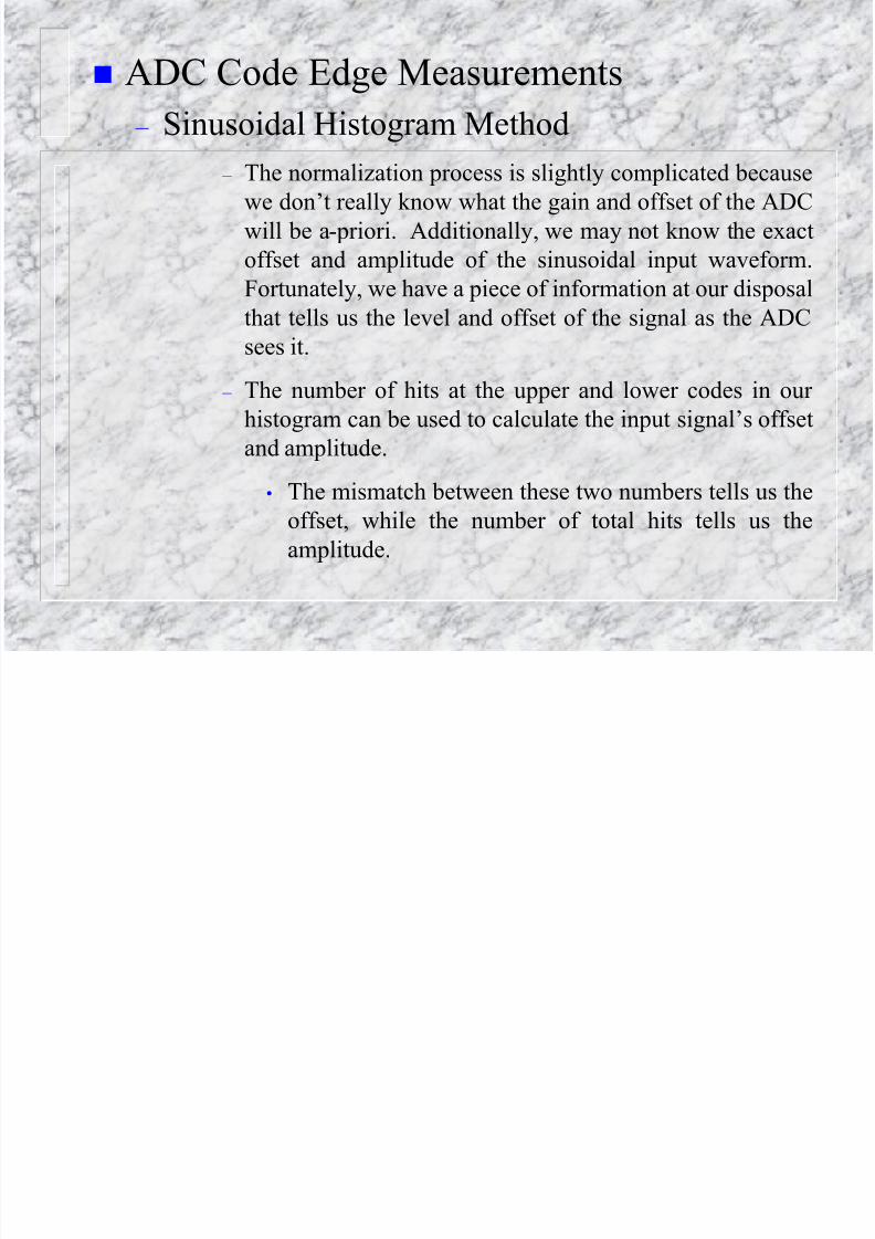
– The normalization process is slightly complicated because
we don’t really know what the gain and offset of the ADC
will be a-priori. Additionally, we may not know the exact
offset and amplitude of the sinusoidal input waveform.
Fortunately, we have a piece of information at our disposal
that tells us the level and offset of the signal as the ADCsees it.
– The number of hits at the upper and lower codes in our
histogram can be used to calculate the input signal’s offset
and amplitude.
• The mismatch between these two numbers tells us the
offset, while the number of total hits tells us the
amplitude.

8/13/2019 Chapter 12 - ADC Testing
http://slidepdf.com/reader/full/chapter-12-adc-testing 48/87
– where N1 is the number of times the upper code is hit, N2
is the number of times the lower code is hit, Ns is the
number of samples, and N is the converter resolution, in
bits.
)1
cos(1 Ns
N C )
2cos(2
Ns
N C
1212
12
)(
1
+
N
C C
C C
LSBsOffset
1
12)(
1
C
Offset LSBs Peak
N

8/13/2019 Chapter 12 - ADC Testing
http://slidepdf.com/reader/full/chapter-12-adc-testing 49/87
ADC Code Edge Measurements
– Sinusoidal Histogram Method
– Once we know the values of Peak and Offset, we can
calculate the ideal distribution of code hits we would
expect from an perfectly linear ADC. This calculation is
performed using equations in Mahoney’s original
publication.
– These equations have been extended for ADCs having any
number of bits of resolution. As Mahoney points out in
his book, these values represent probable numbers of hits
per code, and are therefore not necessarily integers. The
ideal hit counts for each ADC code should be calculated
using floating point calculations.
+
Peak
Offset Codea
Peak
Offset Codea
NsCode IdealCount
N N 11 2sin
21sin)(
8/13/2019 Chapter 12 - ADC Testing
http://slidepdf.com/reader/full/chapter-12-adc-testing 50/87
ADC Code Edge Measurements
– Sinusoidal Histogram Method
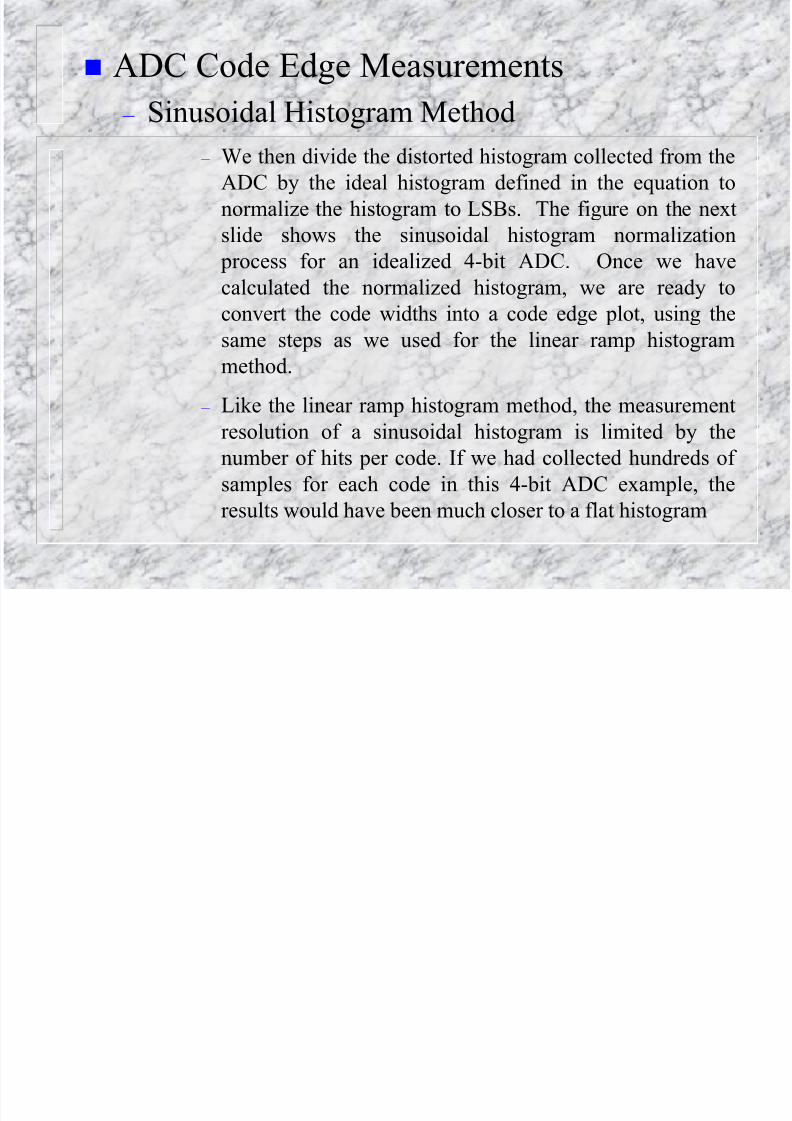
– We then divide the distorted histogram collected from the
ADC by the ideal histogram defined in the equation to
normalize the histogram to LSBs. The figure on the next
slide shows the sinusoidal histogram normalization
process for an idealized 4-bit ADC. Once we have
calculated the normalized histogram, we are ready toconvert the code widths into a code edge plot, using the
same steps as we used for the linear ramp histogram
method.
– Like the linear ramp histogram method, the measurement
resolution of a sinusoidal histogram is limited by the
number of hits per code. If we had collected hundreds of
samples for each code in this 4-bit ADC example, the
results would have been much closer to a flat histogram
80 80

8/13/2019 Chapter 12 - ADC Testing
http://slidepdf.com/reader/full/chapter-12-adc-testing 51/87
Number
of Code
Hits
0
10
20
30
40
50
60
70
Output Code
0 2 4 86 10 14
80
CodeWidth
(LSBs)
12
Divide Measured Number of Hits
by Expected Number of Hits to
Convert Sinusoidal Histogram to
Code Widths
(Width of Lowest and Highest
Codes are Undefined)12
N2
N1
0
10
20
30
40
50
60
70
Output Code
80
Expected Histogram
Undefined
Undefined
Measured Histogram
0 2 4 86 10 1412
0
0.2
0.4
0.6
0.8
1.0
1.2
1.4
Output Code
1.6
Normalized Histogram
0 2 4 86 10 1412
8/13/2019 Chapter 12 - ADC Testing
http://slidepdf.com/reader/full/chapter-12-adc-testing 52/87
DC Tests and Transfer Curve Tests
– DC Gain and Offset
– Once we have produced a code edge transfer curve for an
ADC, we can test the ADC much as we would test a DAC.
Since a code edge transfer curve is a one-to-one mapping
function, we can apply all the same DC and transfer curvetests outlined in Chapter 11, “DAC Testing”.
– There are a few minor differences to consider. For
example, an N-bit ADC has one fewer code edges than an
N-bit DAC has outputs.
– A more important difference is that the ideal ADC transfer
curve may be ambiguously defined. The test engineer
should realize that there are several ways to define the
ideal performance of an ADC.
8/13/2019 Chapter 12 - ADC Testing
http://slidepdf.com/reader/full/chapter-12-adc-testing 53/87
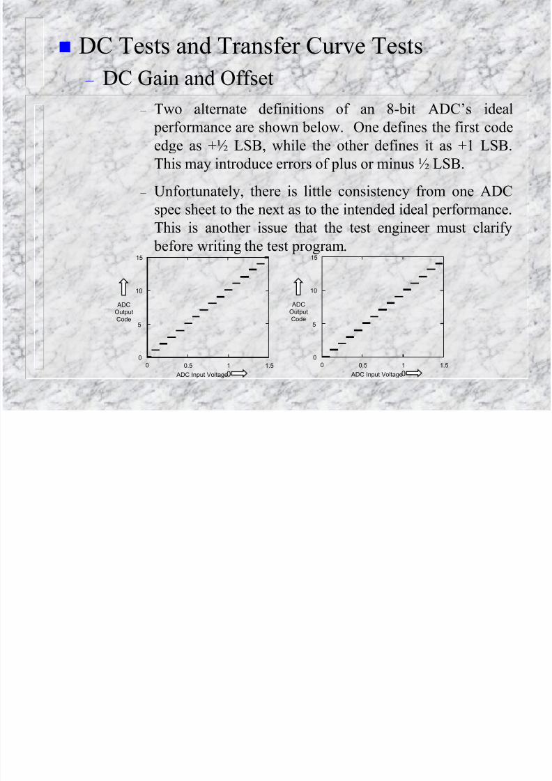
DC Tests and Transfer Curve Tests
– DC Gain and Offset
– Two alternate definitions of an 8-bit ADC’s ideal
performance are shown below. One defines the first code
edge as +½ LSB, while the other defines it as +1 LSB.
This may introduce errors of plus or minus ½ LSB.
– Unfortunately, there is little consistency from one ADCspec sheet to the next as to the intended ideal performance.
This is another issue that the test engineer must clarify
before writing the test program.
ADC
Output
Code
ADC Input Voltage
1.51
00.50
0
5
10
15
ADC
Output
Code
ADC Input Voltage
1.51
00.50
0
5
10
15

8/13/2019 Chapter 12 - ADC Testing
http://slidepdf.com/reader/full/chapter-12-adc-testing 54/87
DC Tests and Transfer Curve Tests
– DC Gain and Offset
– Once the ideal curve has been established, DC gain and offsetcan be measured in a manner similar to DAC DC gain and
offset. The gain and offset are measured by calculating the
slope and offset of the best-fit line. If the converter is defined
using the +1/2 LSB first code edge, we have to remember
that the ideal line has an offset of – ½ LSB.
– Unfortunately, there are many other ways to define gain and
offset. In some spec sheets, the offset is defined simply as
the offset of the first code edge from its ideal position and the
gain is defined as the ratio of the actual voltage range divided
by the ideal voltage range from V-FS to V+FS. Otherdefinitions abound, so the test engineer is responsible for
determining the correct methodology for each ADC to be
tested. Of course, ambiguities in the spec sheet should be
clarified to prevent correlation headaches caused by
misunderstandings in spec definitions.

8/13/2019 Chapter 12 - ADC Testing
http://slidepdf.com/reader/full/chapter-12-adc-testing 55/87
DC Tests and Transfer Curve Tests
– INL and DNL
– Except for the fact that an ADC code edge transfer curve
has one fewer values than an equivalent DAC curve, we
can calculate ADC INL and DNL exactly the same way as
DAC INL and DNL.
– If we use a histogram method, we can take a shortcut inmeasuring INL and DNL. Notice that the LSB sizes in the
normalized histogram are only one computational step
away from an endpoint DNL curve. Subtracting 1 from
each value in the normalized histogram yields the endpoint
DNL curve. – Integrating this curve with a running sum gives us the
endpoint INL curve. Using this shortcut method, we never
even have to compute the absolute voltage level for each
code edge, unless we need that information for a separate
test, like gain of offset.

8/13/2019 Chapter 12 - ADC Testing
http://slidepdf.com/reader/full/chapter-12-adc-testing 56/87
DC Tests and Transfer Curve Tests
– INL and DNL
– As with DAC INL and DNL testing, a best-fit approach is
the preferred method for calculating ADC INL and DNL.
As discussed in Chapter 11, “DAC Testing”, best-fit INL
and DNL testing results in a more meaningful, repeatable
reference line than endpoint testing, since the best-fit
reference line is less dependent on any one code’s value.
– We can convert an endpoint INL curve to a best-fit INL
curve by first calculating the best-fit line for the endpoint
INL curve.
– Subtracting the best-fit line from the endpoint INL curveyields the best-fit INL curve. Then the best-fit DNL curve
is calculated by taking the discrete time first derivative of
the best-fit INL curve.
8/13/2019 Chapter 12 - ADC Testing
http://slidepdf.com/reader/full/chapter-12-adc-testing 57/87
DC Tests and Transfer Curve Tests
– INL and DNL
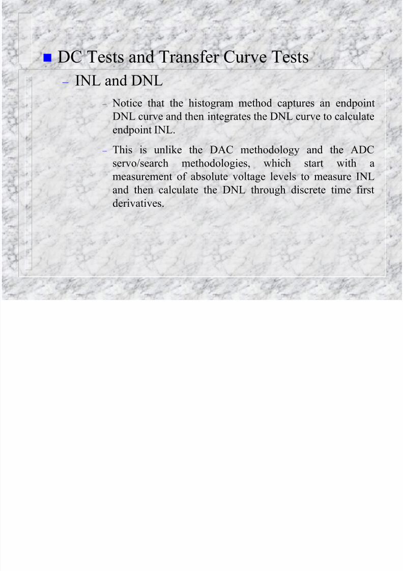
– Notice that the histogram method captures an endpoint
DNL curve and then integrates the DNL curve to calculate
endpoint INL.
– This is unlike the DAC methodology and the ADC
servo/search methodologies, which start with a
measurement of absolute voltage levels to measure INL
and then calculate the DNL through discrete time first
derivatives.
8/13/2019 Chapter 12 - ADC Testing
http://slidepdf.com/reader/full/chapter-12-adc-testing 58/87
DC Tests and Transfer Curve Tests
– Monotonicity and Missing Codes
– One final difference between ADC testing and DAC
testing relates to differences in their weaknesses. For
example, a DAC may be non-monotonic, while an ADC
will always be monotonic if it is tested statically.
– For an ADC to be non-monotonic, one of its code widthswould have to be negative. However, an ADC can appear
to be non-monotonic when its input is changing rapidly.
Therefore, we do not typically test ADCs for monotonicity
when we use slowly changing inputs (as in search or linear
ramp INL and DNL tests).
– However, when testing ADCs with rapidly changing
inputs, the ADC may behave as if it were non-monotonic
due to slew rate limitations in its comparator(s). These
monotonicity errors show up as signal to noise ratio
failures in some ADCs and as sparkling in others.
8/13/2019 Chapter 12 - ADC Testing
http://slidepdf.com/reader/full/chapter-12-adc-testing 59/87
DC Tests and Transfer Curve Tests
– Monotonicity and Missing Codes
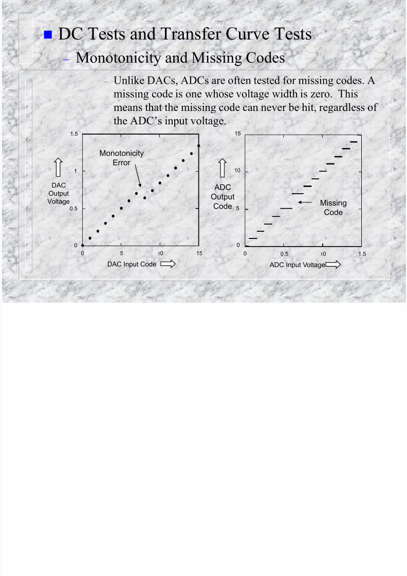
– Unlike DACs, ADCs are often tested for missing codes. A
missing code is one whose voltage width is zero. This
means that the missing code can never be hit, regardless of
the ADC’s input voltage.
DAC
Output
Voltage
DAC Input Code
151050
0
0.5
1
1.5
ADC
Output
Code
ADC Input Voltage
1.5100.50
0
5
10
15
Monotonicity
Error
Missing
Code

8/13/2019 Chapter 12 - ADC Testing
http://slidepdf.com/reader/full/chapter-12-adc-testing 60/87
DC Tests and Transfer Curve Tests
– Monotonicity and Missing Codes
– A missing code shows up as a missing step on an ADC
transfer curve.
– Since DACs always produce a voltage for each input code,
DACs cannot have missing codes.
– Although a true missing code is one that has zero width,
missing codes are often defined as any code having a code
width smaller than some specified value, such as 1/10
LSB. Technically, a code having a width of 1/10 LSB is
not missing, but the chances of it being hit are low enough
that it is considered to be missing from the transfer curve.

8/13/2019 Chapter 12 - ADC Testing
http://slidepdf.com/reader/full/chapter-12-adc-testing 61/87
Dynamic ADC Tests
– Conversion Time, Recovery Time, and
Sampling Frequency – DACs have many dynamic tests such as settling time, rise
and fall time, overshoot and undershoot.
– ADCs do not exhibit these same features, since they donot have an analog output. Instead, an ADC may have any
or all of the following timing specifications:
• maximum sampling frequency
• maximum conversion time
• minimum recovery time
– There are many ways to design ADCs and ADC digital
interfaces

8/13/2019 Chapter 12 - ADC Testing
http://slidepdf.com/reader/full/chapter-12-adc-testing 62/87
Dynamic ADC Tests
– Conversion Time, Recovery Time, and
Sampling Frequency
– The ADC begins a conversion cycle when the CONVERT
signal is asserted high. After the conversion cycle iscompleted, the ADC asserts a DATA_READY signal that
indicates the conversion is complete. Then the data is read
from the ADC using a READ signal.
8/13/2019 Chapter 12 - ADC Testing
http://slidepdf.com/reader/full/chapter-12-adc-testing 63/87
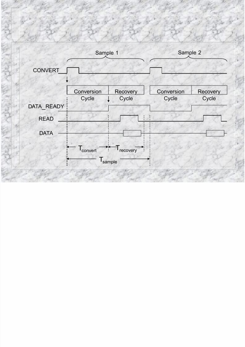
Conversion Cycle
Recovery Cycle
Conversion Cycle
Recovery Cycle
CONVERT
Sample 1
READ
DATA
Tconvert Trecovery
Tsample
Sample 2
DATA _ READY
Dynamic ADC Tests

8/13/2019 Chapter 12 - ADC Testing
http://slidepdf.com/reader/full/chapter-12-adc-testing 64/87
y
– Conversion Time, Recovery Time, and
Sampling Frequency – Maximum conversion time is the maximum amount of
time it takes an ADC to produce a digital output after the
CONVERT signal is asserted. The ADC is guaranteed to
produce a valid output within the maximum conversion
time.
– It is tempting to say that an ADC’s maximum samplingfrequency is simply the inverse of the maximum
conversion time. In many cases this is true. Some ADCs
require a minimum recovery time, which is the minimum
amount of time the system must wait before asserting the
next CONVERT signal. The maximum samplingfrequency is therefore given by the equation:
eryreconvert T T F
cov
max
1
+
8/13/2019 Chapter 12 - ADC Testing
http://slidepdf.com/reader/full/chapter-12-adc-testing 65/87
8/13/2019 Chapter 12 - ADC Testing
http://slidepdf.com/reader/full/chapter-12-adc-testing 66/87
Dynamic ADC Tests
– Conversion Time, Recovery Time, andSampling Frequency
– In many ADC designs, the CONVERT signal is generated
automatically after the ADC output data is read. This type
of converter requires no externally supplied CONVERTsignal.
– Sometimes ADCs simply perform continuous conversions
at a constant sampling rate. The CONVERT signal is
generated at a fixed frequency derived from the device
master clock. This architecture is very common in ADCchannels such as those in a cellular telephone voice band
interface or multimedia audio device.
8/13/2019 Chapter 12 - ADC Testing
http://slidepdf.com/reader/full/chapter-12-adc-testing 67/87
Dynamic ADC Tests
– Sparkling
– Sparkling is a phenomenon that happens most often in
high speed flash converters due to digital timing race
conditions. It is the tendency for an ADC to occasionally
produce a conversion that has a larger than expected offset
from the expected value.
– We can think of a sparkle sample as one that is a statistical
outlier from the Gaussian distribution.
– Sparkling shows up in a time domain plot as sudden
variations from the expected values. It got its name from
early flash ADC applications, in which the sample outliers produced white sparkles on a video display.

8/13/2019 Chapter 12 - ADC Testing
http://slidepdf.com/reader/full/chapter-12-adc-testing 68/87
Dynamic ADC Tests
– Sparkling
– Sparkling is specified as a maximum acceptable deviationfrom the expected conversion result. For example, we
might see a specification that states sparkling will be less
than 2 LSBs, meaning that we will never see a sample that
is more than 2 LSBs from the expected value.
Output
Code
0
1
2
3
4
5
6
7
Input Voltage
(mV)
0 10 20 4030 50 60 70 80 90

8/13/2019 Chapter 12 - ADC Testing
http://slidepdf.com/reader/full/chapter-12-adc-testing 69/87
Dynamic ADC Tests
– Sparkling
– Test methodologies for sparkling vary, mainly in the
choice of input signal. We might look for sparkling in our
ramp histogram raw data. We might also apply a very
high frequency sine wave to the ADC and look for time
domain spikes in the collected samples.
– Since it is a random digital failure process, sparkling often
produces intermittent test results.
– Sparkling is generally caused by a weakness in the ADC
design that must be eliminated through good design
margin rather than being screened out by testing.
– Nevertheless, ADC sparkling tests are sometimes added
to a program as a quick sanity check, making use of
samples collected for one of the required parametric tests.

8/13/2019 Chapter 12 - ADC Testing
http://slidepdf.com/reader/full/chapter-12-adc-testing 70/87
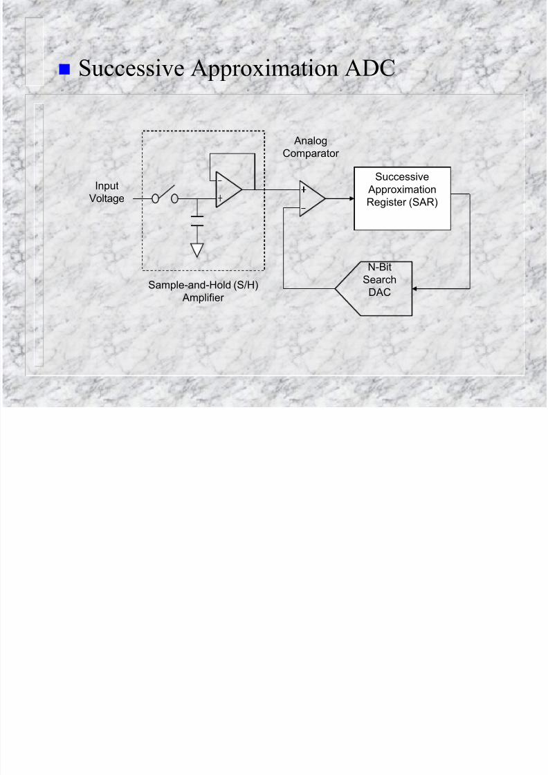
ADC Architectures
– Successive Approximation Architectures – Many ADCs are designed using a successive
approximation architecture, in which a DAC output is
adjusted with a binary search algorithm until it is
substantially equal to the ADC input voltage.
– The comparison between the input voltage and the DAC’s
binary search voltage is performed by an analog
comparator.
– Successive approximation register (SAR) logic controls
the binary search process, moving the DAC value up ordown depending on the result of the comparison.
– Once the binary search process is complete, the SAR value
(i.e. the DAC’s input code) represents the ADC’s
conversion result.
8/13/2019 Chapter 12 - ADC Testing
http://slidepdf.com/reader/full/chapter-12-adc-testing 71/87
Successive Approximation ADC
Successive
Approximation
Register (SAR)
N-Bit
Search
DAC
Input
Voltage
Sample-and-Hold (S/H)
Amplifier
Analog
Comparator
8/13/2019 Chapter 12 - ADC Testing
http://slidepdf.com/reader/full/chapter-12-adc-testing 72/87
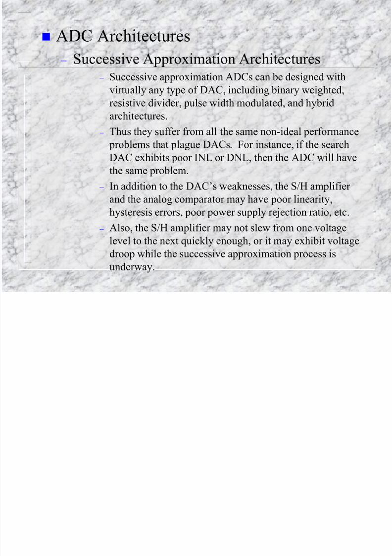
ADC Architectures
– Successive Approximation Architectures – Successive approximation ADCs can be designed with
virtually any type of DAC, including binary weighted,
resistive divider, pulse width modulated, and hybrid
architectures.
– Thus they suffer from all the same non-ideal performance
problems that plague DACs. For instance, if the searchDAC exhibits poor INL or DNL, then the ADC will have
the same problem.
– In addition to the DAC’s weaknesses, the S/H amplifier
and the analog comparator may have poor linearity,
hysteresis errors, poor power supply rejection ratio, etc. – Also, the S/H amplifier may not slew from one voltage
level to the next quickly enough, or it may exhibit voltage
droop while the successive approximation process is
underway.

8/13/2019 Chapter 12 - ADC Testing
http://slidepdf.com/reader/full/chapter-12-adc-testing 73/87
ADC Architectures
– Integrating ADCs (Dual Slope and Single
Slope)
– If a successive approximation ADC is analogous to a
binary search, then a dual-slope ADC is analogous to a
step search.
– A dual-slope ADC is much simpler but much slower thana successive approximation ADC in the same way that a
step search is much slower than a binary search.
– Instead of a search DAC, it uses a simple integrator to
ramp upward for a fixed amount of time, TIntegration, starting
from the time it crosses a fixed threshold voltage
– The slope of integration is directly proportional to the
analog input voltage.

8/13/2019 Chapter 12 - ADC Testing
http://slidepdf.com/reader/full/chapter-12-adc-testing 74/87
ADC Architectures
– Integrating ADCs – Therefore, the larger the input voltage, the higher the
integration voltage will be at the end of the fixed time
period. Then the integrator is ramped downward at a fixed
slope until it reaches the threshold voltage again. The
time it takes to discharge is directly proportional to the
integrator’s peak voltage, which in turn is proportional tothe ADC input voltage.
– The time period Tcount is measured by a digital counter,
whose output therefore represents the ADC conversion
result. Because the integrator ramps up and then down,
this type of converter is called a dual-slope ADC.

8/13/2019 Chapter 12 - ADC Testing
http://slidepdf.com/reader/full/chapter-12-adc-testing 75/87
Conversion
Result
Threshold
Voltage
N-Bit Counter
and
Control Logic
Input
Voltage
AnalogIntegrator
Analog
Comparator
Threshold
Voltage
Integration Control
Fixed Slope
TIntegration
(Fixed)
Reset Reset
Tcount
(Proportional to
Vin)
Slope Proportional to
Input Voltage, Vin
8/13/2019 Chapter 12 - ADC Testing
http://slidepdf.com/reader/full/chapter-12-adc-testing 76/87
ADC Architectures
– Integrating ADCs – Single-slope ADCs work in a similar manner, but only
count the time it takes the integrator output to ramp from
an initial voltage to a threshold voltage. The integrator
only ramps in one direction. Single-slope ADCs are
simpler in nature than dual-slope ADCs, but they typically
suffer from worse offset errors. Dual-slope ADCs are also
more immune to linearity errors in the integrator because
the linearity errors in the upward ramp cancel the linearity
errors in the downward ramp.
ADC A hi

8/13/2019 Chapter 12 - ADC Testing
http://slidepdf.com/reader/full/chapter-12-adc-testing 77/87
ADC Architectures
– Integrating ADCs - Testing
– The conversion time of a single- or dual-slope ADC istypically quite long, perhaps 100 ms or more. Therefore,
all-codes testing would be prohibitively expensive for
production testing of most integrating ADCs.
– By their nature, integrating ADCs have excellent DNL
characteristics, since each code width is dependent on asmoothly ramping analog integrator rather than a binary
weighted sum of electrical components.
– However, integrating ADCs may be susceptible to INL
errors. The INL curve is dominated by the linearity of the
comparator and the linearity of the integrator’s ramp, bothof which tend to have simple bends rather than complex
shapes

8/13/2019 Chapter 12 - ADC Testing
http://slidepdf.com/reader/full/chapter-12-adc-testing 78/87
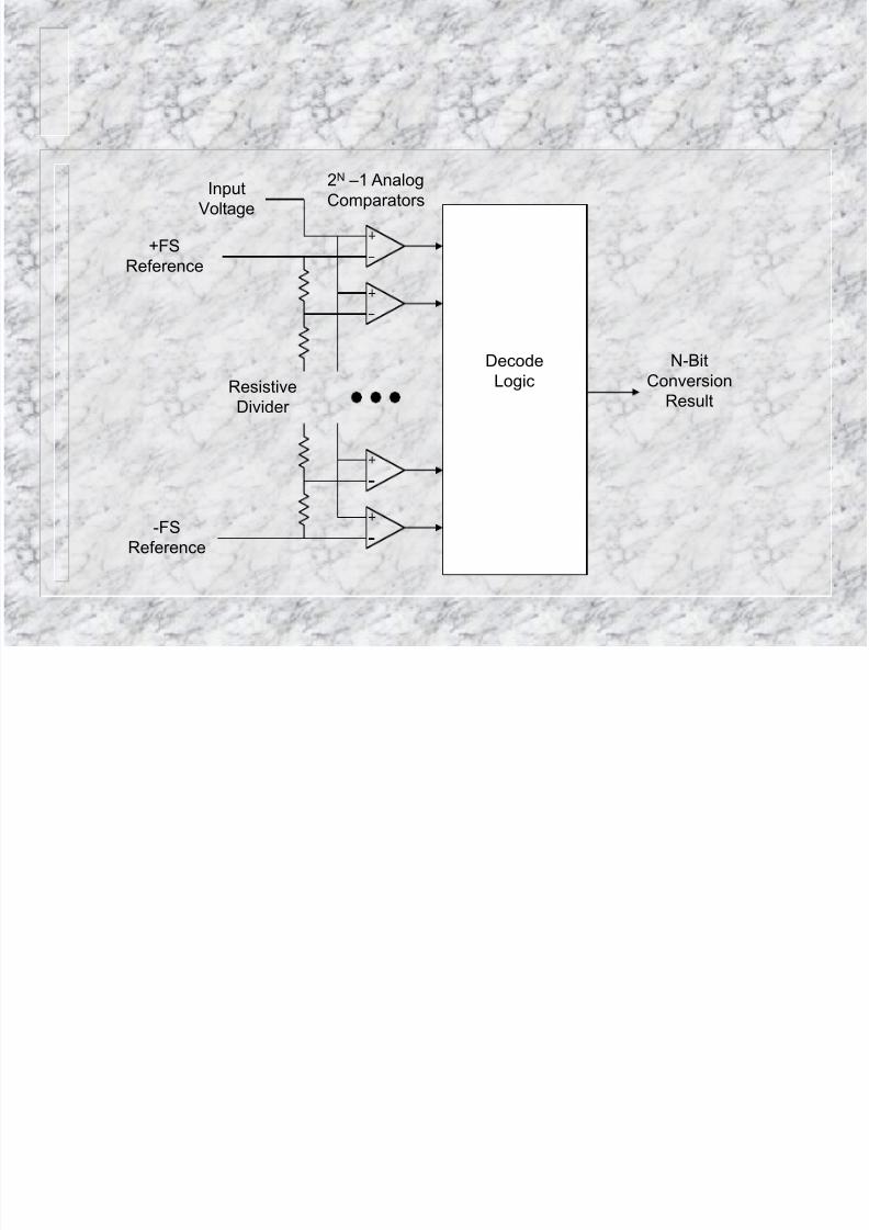
ADC Architectures
– Flash ADCs – Flash ADCs are somewhat analogous to resistive divider
DACs. A flash conversion is a brute force means of
comparing the input signal against all possible decision
levels, simultaneously. This requires 2 N – 1 comparators
for an N-bit ADC. Digital decode logic determines which
of the comparators producing a logic one has the highest
threshold voltage. The number of the comparator
represents the ADC output code. Like the resistive divider
DAC, the flash converter must be tested for all codes,
since any resistor or any comparator may be defective
8/13/2019 Chapter 12 - ADC Testing
http://slidepdf.com/reader/full/chapter-12-adc-testing 79/87
N-Bit
Conversion
Result
Decode
Logic
Input
Voltage
Resistive
Divider
2N –1 Analog
Comparators
+FS
Reference
-FS
Reference
8/13/2019 Chapter 12 - ADC Testing
http://slidepdf.com/reader/full/chapter-12-adc-testing 80/87
ADC Architectures
– Flash ADCs – The flash ADC is much faster than a successive
approximation ADC because the decision levels are
compared all at once.
–
No S/H amplifier is required for a flash ADC becausethere is no need to hold the input constant. Since a
separate comparator is required for each decision level, the
flash ADC becomes prohibitively expensive as resolution
increases beyond a few bits.
– The flash ADC architecture is mostly used in very high
frequency applications that can tolerate the high silicon
area required by the many comparators.

8/13/2019 Chapter 12 - ADC Testing
http://slidepdf.com/reader/full/chapter-12-adc-testing 81/87
ADC Architectures
– PDM (Sigma Delta) ADCs – Sigma-delta ADCs are similar to sigma-delta DACs in
terms of their operating theory.
– Sigma-delta analog-to-digital converters use a crude ADC
(typically an analog comparator) combined with a noiseshaping process to produce an oversampled pulse density
modulated (PDM) data stream.
– This data stream is then digitally filtered and decimated to
produce high resolution ADC samples.
– The high resolution and excellent linearity of sigma-deltaADCs make them ideal for audio and modulated data
applications like modems, PC sound cards, and cellular
telephones.
8/13/2019 Chapter 12 - ADC Testing
http://slidepdf.com/reader/full/chapter-12-adc-testing 82/87
Tests for Common ADC Applications
– DC Measurements
– An ADC may be used to measure absolute voltage levels,
as in a DC voltmeter or battery monitor.
– Don’t usually care about transmission parameters like
signal to noise ratio.
– We will typically only need to know the DC gain, DCoffset, INL, DNL, and worst-case absolute voltage errors
in decision levels, relative to the ideal decision levels. Idle
channel noise will sometimes be specified, to insure that
results obtained from the ADC are not unrepeatable due to
excessive noise.
– Successive approximation ADCs and integrating ADCs
are the most common converter type used for DC
measurements.
f li i

8/13/2019 Chapter 12 - ADC Testing
http://slidepdf.com/reader/full/chapter-12-adc-testing 83/87
Tests for Common ADC Applications
– Audio Digitization
– Audio digitization is a very common application for
ADCs, especially high resolution ADCs.
– When the resolution exceeds 12 or 13 bits, it becomes
very expensive to perform transfer curve tests such as INL
and DNL because of all the code edges that must bemeasured.
– Transmission parameters such as frequency response,
signal to distortion ratio, idle channel noise, etc. are more
meaningful measures of audio digitizer performance.
These sampled channel tests are much less time-consuming to measure than INL and DNL.
– Sigma delta ADCs have become the most common
architecture for audio digitization application.
T f C ADC A li i

8/13/2019 Chapter 12 - ADC Testing
http://slidepdf.com/reader/full/chapter-12-adc-testing 84/87
Tests for Common ADC Applications
– Data Transmission
– Data transmission applications differ from audio
applications mainly in terms of the sampling rates and the
frequency range of the transmitted signals.
– Data transmission ADCs, such as those found in modems,
hard disk drive read channels, and cellular telephoneintermediate frequency (IF) sections, often digitize signals
that are well above the audio band.
– Typically require lower resolution ADCs, but may require
much higher sampling rates. Aperture jitter is often a
prime concern for these applications, especially if thesignal frequency band extends past a few tens of
megahertz. Excessive aperture jitter can introduce
apparent noise in the digitized signal, ruining the
performance of the ADC.
8/13/2019 Chapter 12 - ADC Testing
http://slidepdf.com/reader/full/chapter-12-adc-testing 85/87
Tests for Common ADC Applications
– Data Transmission
– Signal to noise ratio, group delay distortion, and other
transmission parameters are often specified in data
transmission applications. Also, data transmission
specifications such as error vector magnitude (EVM), phase trajectory error (PTE), and bit error rate (BER) may
also need to be tested.
– Most ADC architectures are well suited for low frequency
data transmission applications (with the exception of
integrating converters). High frequency applications mayrequire fast successive approximation ADCs, semi-flash
ADCs, or even full flash ADCs, depending on the required
sampling rates.
8/13/2019 Chapter 12 - ADC Testing
http://slidepdf.com/reader/full/chapter-12-adc-testing 86/87
Tests for Common ADC Applications
– Video Digitization
– NTSC video signal digitization is another key application
for high speed ADCs.
– These applications require the faster ADC types (flash,
semi-flash, or pipelined successive approximation ADCs).
– The test list for these types of converters usually includes
transmission parameters as well as differential gain and
differential phase measurements. Like other high speed
applications, aperture jitter is a key performance
specification for video digitization applications. Sparkling
is particularly noticeable in video applications, so this
potential weakness should be thoroughly characterized
and/or tested in production.
8/13/2019 Chapter 12 - ADC Testing
http://slidepdf.com/reader/full/chapter-12-adc-testing 87/87
Summary
ADC testing is very closely related to DAC testing.
Many of the DC and intrinsic tests defined in this
chapter are very similar to those performed on
DACs. The most important difference is that the
ADC code edge transfer curve is harder and muchmore time consuming to measure than the DAC
transfer curve. However, once the many-to-one
statistical mapping of an ADC has been converted to
a one-to-one code edge transfer curve, the DC and
transfer curve tests are very similar in nature to
those encountered in DAC testing.