
Chapter 1 Introduction - Home - IOE Notes Chapter 1 : Introduction Compiled by: Er. Hari Aryal...
15
Microprocessors Chapter 1 : Introduction Compiled by: Er. Hari Aryal Email: [email protected] Reference: Ramesh S. Gaonkar | 1 Chapter – 1 Introduction 1.1 Introduction A Microprocessor is a multipurpose programmable, clock driven, register based electronic device that reads binary instructions from a storage device called memory, accepts binary data as input, processes data according to those instructions and provide result s as output. The microprocessor operates in binary 0 and 1 known as bits are represented in terms of electrical voltages in the machine that means 0 represents low voltage level and 1 represents high voltage level. Each microprocessor recognizes and processes a group of bits called the word and microprocessors are classified according to their word length such as 8 bits microprocessor with 8 bit word and 32 bit microprocessor with 32 bit word etc. Fig 1.1: A Programmable Machine Terms used CPU: - Central processing unit which consists of ALU and control unit. Microprocessor: - Single chip containing all units of CPU. Microcomputer: - Computer having microprocessor as CPU. Microcontroller: single chip consisting of MPU, memory, I/O and interfacing circuits. MPU: - Microprocessing unit – complete processing unit with the necessary control signals. 1.2 Basic Block Diagram of a Computer Traditionally, the computer is represented with four components such as memory, input, output and central processing unit (CPU) which consists of arithmetic logic unit (ALU) and control unit (CU).
Transcript of Chapter 1 Introduction - Home - IOE Notes Chapter 1 : Introduction Compiled by: Er. Hari Aryal...

Microprocessors Chapter 1 : Introduction
Compiled by: Er. Hari Aryal Email: [email protected] Reference: Ramesh S. Gaonkar | 1
Chapter – 1
Introduction
1.1 Introduction
A Microprocessor is a multipurpose programmable, clock driven, register based electronic device that reads binary instructions from a storage device called memory, accepts binary data as input, processes data according to those instructions and provide result s as output. The microprocessor operates in binary 0 and 1 known as bits are represented in terms of electrical voltages in the machine that means 0 represents low voltage level and 1 represents high voltage level. Each microprocessor recognizes and processes a group of bits called the word and microprocessors are classified according to their word length such as 8 bits microprocessor with 8 bit word and 32 bit microprocessor with 32 bit word etc.
Fig 1.1: A Programmable Machine
Terms used
CPU: - Central processing unit which consists of ALU and control unit.
Microprocessor: - Single chip containing all units of CPU.
Microcomputer: - Computer having microprocessor as CPU.
Microcontroller: single chip consisting of MPU, memory, I/O and interfacing circuits.
MPU: - Microprocessing unit – complete processing unit with the necessary control signals.
1.2 Basic Block Diagram of a Computer
Traditionally, the computer is represented with four components such as memory, input,
output and central processing unit (CPU) which consists of arithmetic logic unit (ALU) and
control unit (CU).

Microprocessors Chapter 1 : Introduction
Compiled by: Er. Hari Aryal Email: [email protected] Reference: Ramesh S. Gaonkar | 2
Fig 1.2 (a): Traditional Block diagram of a computer
The CPU contains various registers to store data, the ALU to perform arithmetic and logical
operations, instruction decoders, counters and control lines.
The CPU reads instructions from memory and performs the tasks specified. It communicates
with input/output (I/O) devices either to accept or to send data, the I/O devices is known as
peripherals.
Later on around late 1960’s, traditional block diagram can be replaced with computer having
microprocessor as CPU which is known as microcomputer. Here CPU was designed using
integrated circuit technology (IC’s) which provided the possibility to build the CPU on a single
chip.
Fig 1.2 (b): Block Diagram of a computer with the Microprocessor as CPU
Later on semiconductor fabrication technology became more advanced, manufacturers were
able to place not only MPU but also memory and I/O interfacing circuits on a single chip known
as microcontroller, which also includes additional devices such as A/D converter, serial I/O,
timer etc.

Microprocessors Chapter 1 : Introduction
Compiled by: Er. Hari Aryal Email: [email protected] Reference: Ramesh S. Gaonkar | 3
Fig 1.2 (c): Block Diagram of a Microcontroller
1.3 Organization of a microprocessor based system
Microprocessor based system includes there components microprocessor, input/output and
memory (read only and read/write). These components are organized around a common
communication path called a bus.
Fig 1.3: Microprocessor Based System with Bus Architecture
Microprocessor:
It is clock driven semiconductor device consisting of electronic logic circuits manufactured by
using either a large scale integration (LSI) or very large scale integration (VLSI) technique. It is
capable of performing various computing functions and making decisions to change the
sequence of program execution. It can be divided in to three segments.
A. Arithmetic/Logic unit: It performs arithmetic operations as addition and subtraction and
logic operations as AND, OR & XOR.
Microprocessors Chapter 1 : Introduction
Compiled by: Er. Hari Aryal Email: [email protected] Reference: Ramesh S. Gaonkar | 4
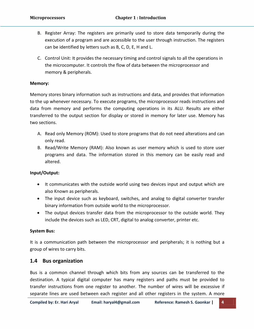
B. Register Array: The registers are primarily used to store data temporarily during the
execution of a program and are accessible to the user through instruction. The registers
can be identified by letters such as B, C, D, E, H and L.
C. Control Unit: It provides the necessary timing and control signals to all the operations in
the microcomputer. It controls the flow of data between the microprocessor and
memory & peripherals.
Memory:
Memory stores binary information such as instructions and data, and provides that information
to the up whenever necessary. To execute programs, the microprocessor reads instructions and
data from memory and performs the computing operations in its ALU. Results are either
transferred to the output section for display or stored in memory for later use. Memory has
two sections.
A. Read only Memory (ROM): Used to store programs that do not need alterations and can
only read.
B. Read/Write Memory (RAM): Also known as user memory which is used to store user
programs and data. The information stored in this memory can be easily read and
altered.
Input/Output:
It communicates with the outside world using two devices input and output which are
also Known as peripherals.
The input device such as keyboard, switches, and analog to digital converter transfer
binary information from outside world to the microprocessor.
The output devices transfer data from the microprocessor to the outside world. They
include the devices such as LED, CRT, digital to analog converter, printer etc.
System Bus:
It is a communication path between the microprocessor and peripherals; it is nothing but a
group of wires to carry bits.
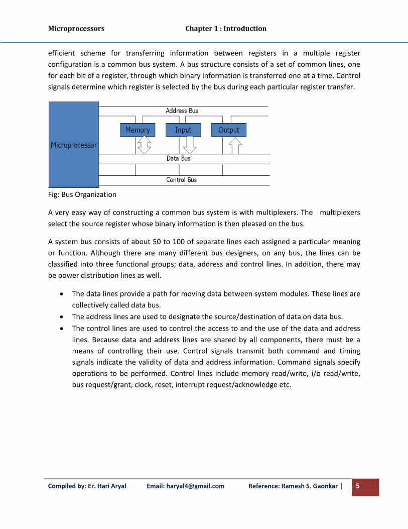
1.4 Bus organization
Bus is a common channel through which bits from any sources can be transferred to the
destination. A typical digital computer has many registers and paths must be provided to
transfer instructions from one register to another. The number of wires will be excessive if
separate lines are used between each register and all other registers in the system. A more
Microprocessors Chapter 1 : Introduction
Compiled by: Er. Hari Aryal Email: [email protected] Reference: Ramesh S. Gaonkar | 5
efficient scheme for transferring information between registers in a multiple register
configuration is a common bus system. A bus structure consists of a set of common lines, one
for each bit of a register, through which binary information is transferred one at a time. Control
signals determine which register is selected by the bus during each particular register transfer.
Fig: Bus Organization
A very easy way of constructing a common bus system is with multiplexers. The multiplexers
select the source register whose binary information is then pleased on the bus.
A system bus consists of about 50 to 100 of separate lines each assigned a particular meaning
or function. Although there are many different bus designers, on any bus, the lines can be
classified into three functional groups; data, address and control lines. In addition, there may
be power distribution lines as well.
The data lines provide a path for moving data between system modules. These lines are
collectively called data bus.
The address lines are used to designate the source/destination of data on data bus.
The control lines are used to control the access to and the use of the data and address
lines. Because data and address lines are shared by all components, there must be a
means of controlling their use. Control signals transmit both command and timing
signals indicate the validity of data and address information. Command signals specify
operations to be performed. Control lines include memory read/write, i/o read/write,
bus request/grant, clock, reset, interrupt request/acknowledge etc.

Microprocessors Chapter 1 : Introduction
Compiled by: Er. Hari Aryal Email: [email protected] Reference: Ramesh S. Gaonkar | 6
Historical Background of the Development of Computers:
The most efficient and versatile electronic machine computer is basically a development of a calculator which leads to the development of the computer. The older computer were mechanical and newer are digital. The mechanical computer namely difference engine and analytical engine developed by Charles Babbage the father of the computer can be considered as the forerunners of modern digital computers.
The difference engine was a mechanical device that could add and subtract and could only run a single algorithm. It’s output system was incompatible to write on punched cards and early optical disks. The ‘analytical engine’ provided more advanced features. It consisted mainly four components the store (memory), the mill (computation unit) , input section (punched card reader) and output section (punched and printed output). The store consisted of 1000s of words of 50 decimal digits used to hold variables and results. The mill could accept operands from the store, add, subtract, multiply or divide them and return a result to the store.
The evolution of the vacuum tubes led the development of computer into a new era. The world’s first general purpose electronic digital computer was ENIAC (Electronic Numerical Integrator and Calculator) built by using vacuum tubes was enormous in size and consumed very high power. However it was faster than mechanical computers. The ENIAC was decimal machine and performed only decimal numbers. Its memory consisted of 20 ‘accumulators’ each capable of holding 10 digits decimal numbers. Each digit was represented by a ring of 10 vacuum tubes. ENIAC had to be programmed manually by setting switches and plugging and unplug a cable which was the main drawback of it.
Automated calculator:
It is a data processing device that carries out logic and arithmetic operations but has limited programming capability for the user. It accepts data from a small keyboard one digit at a time performs required arithmetic and logical calculations and stores the result on visual display like LCD or LED. The calculator’s programs are stored in ROM’s while the data is stored in RAM.
Some important features of automated calculations:
The ability to interface easily with keyboards and displays.
The ability to handle decimal digits, the device is able to handle more than 4 bits at a time.
Ability to execute the standard programs stored in read only memory.
Extendibility, so that mathematical functions such as %, √, trigonometric, statistical etc. can be easily executed.
Flexibility so it can be used in engineering business or programming without a complete new design.
Low cost, small size and low power consumptions.
Microprocessors Chapter 1 : Introduction
Compiled by: Er. Hari Aryal Email: [email protected] Reference: Ramesh S. Gaonkar | 7
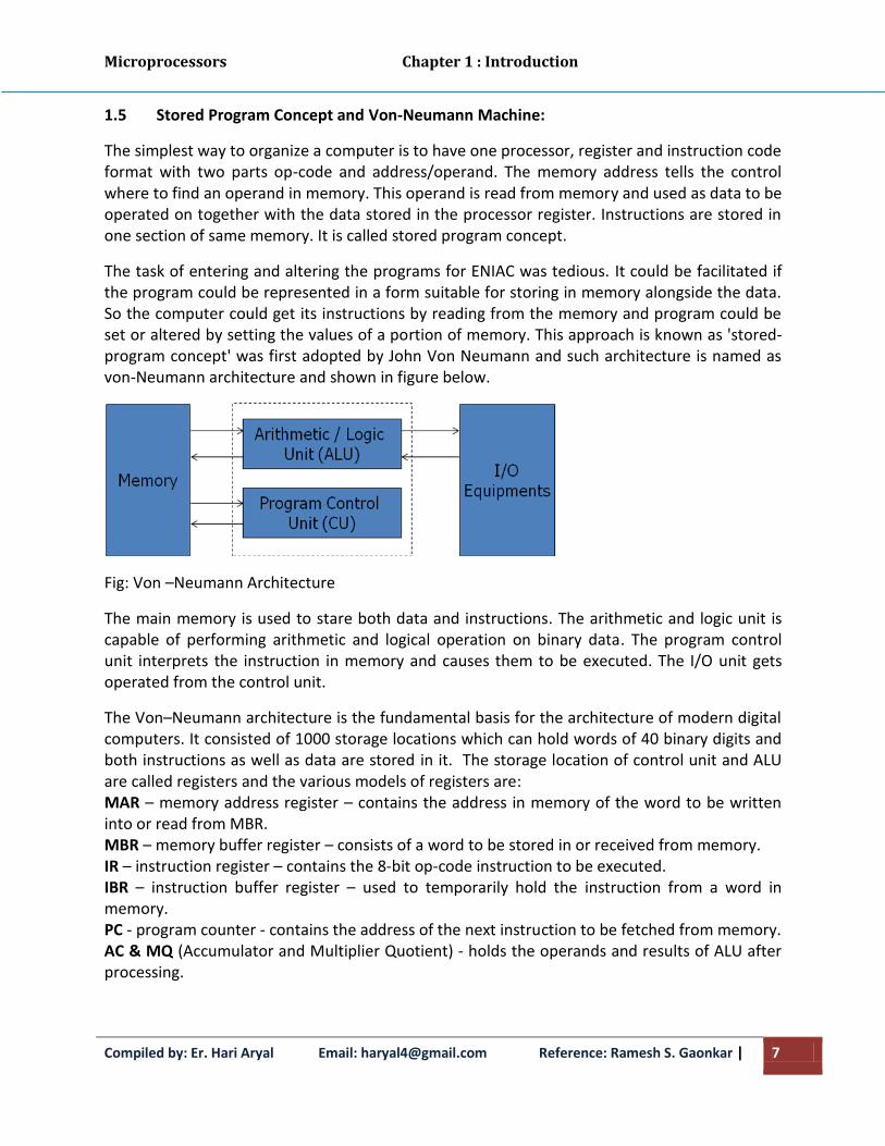
1.5 Stored Program Concept and Von-Neumann Machine:
The simplest way to organize a computer is to have one processor, register and instruction code format with two parts op-code and address/operand. The memory address tells the control where to find an operand in memory. This operand is read from memory and used as data to be operated on together with the data stored in the processor register. Instructions are stored in one section of same memory. It is called stored program concept.
The task of entering and altering the programs for ENIAC was tedious. It could be facilitated if the program could be represented in a form suitable for storing in memory alongside the data. So the computer could get its instructions by reading from the memory and program could be set or altered by setting the values of a portion of memory. This approach is known as 'stored- program concept' was first adopted by John Von Neumann and such architecture is named as von-Neumann architecture and shown in figure below.
Fig: Von –Neumann Architecture
The main memory is used to stare both data and instructions. The arithmetic and logic unit is capable of performing arithmetic and logical operation on binary data. The program control unit interprets the instruction in memory and causes them to be executed. The I/O unit gets operated from the control unit.
The Von–Neumann architecture is the fundamental basis for the architecture of modern digital computers. It consisted of 1000 storage locations which can hold words of 40 binary digits and both instructions as well as data are stored in it. The storage location of control unit and ALU are called registers and the various models of registers are: MAR – memory address register – contains the address in memory of the word to be written into or read from MBR. MBR – memory buffer register – consists of a word to be stored in or received from memory. IR – instruction register – contains the 8-bit op-code instruction to be executed. IBR – instruction buffer register – used to temporarily hold the instruction from a word in memory. PC - program counter - contains the address of the next instruction to be fetched from memory. AC & MQ (Accumulator and Multiplier Quotient) - holds the operands and results of ALU after processing.

Microprocessors Chapter 1 : Introduction
Compiled by: Er. Hari Aryal Email: [email protected] Reference: Ramesh S. Gaonkar | 8
Harvard Architecture In von-Neumann architecture, the same memory is used for storing instructions and data. Similarly, a single bus called data bus or address bus is used for reading data and instructions from or writing to memory. It also had limited the processing speed for computers. The hardvard architecture based computer consists of separate memory spaces for the programs (instructions) and data. Each space has its own address and data buses. So instructions and data can be fetched from memory concurrently and provides significance processing speed improvement. In figure below, there are two data and two address buses multiplexed for data bus and address bus. Hence, there are two blocks of RAM chips one for program memory and another for data memory addresses.
Fig: Harvard Architecture Based Microprocessor The control unit controls the sequence of operations. Central ALU consists of ALU, multiplier, accumulator and scaling chief register. The PC used to address program memory and always contains the address of next instruction to be executed. Here data and control buses are bidirectional and address bus is unidirectional. Evolution of Microprocessors (Intel series) The CPU of a computer consists of ALU, CU and memory. If all these components can be organized on a single chip by means of SSI, MSI, LSI, VLSI, ULSI, ELSI technology, then such chip is called microprocessor. It can fetch instructions from memory, decode and execute them, perform logical and arithmetic functions, accept data from input devices and send results to the output devices. The evolution of microprocessor is dependent on the development of integrated circuit technology from single scale integration (SSI) to giga scale integration (GSI).
Microprocessors Chapter 1 : Introduction
Compiled by: Er. Hari Aryal Email: [email protected] Reference: Ramesh S. Gaonkar | 9
Date Microprocessor Data bus Address Bus Memory
1971 4004 4-bit 10-bit 640 Bytes
1972 8008 8-bit 14-bit 16k
1974 8080 8bit 16bit 64k
1976 8085 8bit 16b it 64k
1978 8086 16bit 20bit 1M
1979 8088 8bit 20bit 1M
1982 80286 16bit 24bit 16M
1985 80386 32bit 32bit 4G
1989 80486 32bit 32bit 4G
1993 Pentium 32/64bit 32bit 4G
1995 Pentium pro 32/64bit 36bit 64G
1997 Pentium II 64bit 36bit 64G
1998 Celeron 64bit 36bit 64G
1999 Pentium III 64bit 36bit 64G
2000 Pentium IV 64bit 36bit 64G
2001 Itanium 128 bit 64bit 64G
2002 Itanium 2 128 bit 64bit 64G
2003 Pentium M/Centrino (wireless capability) for Mobile version e.g. Laptop
Core 2: X86 – 64 Architecture
1.6 Processing Cycle of a Stored Program Computer
Fetch
Identify
Fetch Data
Process
Write Back 1.7 Microinstructions and Hardwired/Microprogrammed Control Unit
Micro-Operations
• A computer executes a program consisting instructions. Each instruction is made up of shorter sub-cycles as fetch, indirect, execute cycle, and interrupt.
• Performance of each cycle has a number of shorter operations called micro-operations. • Called so because each step is very simple and does very little. • Thus micro-operations are functional atomic operation of CPU. • Hence events of any instruction cycle can be described as a sequence of micro-
operations.

Microprocessors Chapter 1 : Introduction
Compiled by: Er. Hari Aryal Email: [email protected] Reference: Ramesh S. Gaonkar | 10
Microinstructions
Each instruction is characterized with many machine cycles and each cycle is characterized with
many T-states. The lower instruction level patterns which are the numerous sequences for a
single instruction are known as microinstructions. Suppose we can visualize the
microinstruction with the help of fetch cycle, or read cycle or write cycle.
Fetch – Registers
• Memory Address Register (MAR) – Connected to address bus – Specifies address for read or write op
• Memory Buffer Register (MBR) – Connected to data bus – Holds data to write or last data read
• Program Counter (PC) – Holds address of next instruction to be fetched
• Instruction Register (IR) – Holds last instruction fetched
Fetch Sequence
• Address of next instruction is in PC • Address (MAR) is placed on address bus • Control unit issues READ command • Result (data from memory) appears on data bus • Data from data bus copied into MBR • PC incremented by 1 (in parallel with data fetch from memory) • Data (instruction) moved from MBR to IR • MBR is now free for further data fetches
Fetch Sequence (symbolic)
(tx = time unit/clock cycle)
• t1: MAR <- PC • t2: MBR <- (memory or MAR) • t3: PC <- PC +1 IR <- MBR
Microprocessors Chapter 1 : Introduction
Compiled by: Er. Hari Aryal Email: [email protected] Reference: Ramesh S. Gaonkar | 11
OR
• t1: MAR <- PC • t2: MBR <- (memory or MAR) PC <- PC +1
• t3: IR <- MBR
Control Unit
The control unit is the heart of CPU. It gets instruction from memory. The control unit decides
what the instructions mean and directs the necessary data to be moved from memory to ALU.
It must communicate with both ALU and main memory. It coordinates all activities of processor
unit, peripheral devices and storage devices. Two types of control unit can be implemented in
computing systems.
1. Hardwired Control Unit • This CU is essentially a combinatorial circuit. It’s i/p logic signals are transformed into set
of o/p logic signals which are control signals. • The CU performs different operations in the basis of op-codes. • We have to derive the Boolean expression for each control signal as a function of input. • Since modern processor needs a Boolean equation, it is very difficult to build a
combinational circuit that satisfies all these operations. • It has faster mode of operation. • A hardwired control unit needs rewiring if design has to be modified.
2. Micro-programmed Control Unit • An alternative to hardwired CU. • In micro-programmed control unit, the control information is stored in control memory. • The control memory is programmed to initiate required sequence of operations. • Use sequences of instructions to perform control operations performed by micro
operations. • Control address register contains the address of the next microinstruction to be read • As it is read, it is transferred to control buffer register. • Sequencing unit loads the control address register and issues a read command. • It is cheaper and simple than hardwired CU. • It is slower than hardwired CU.
1.8 Introduction to Register Transfer Language (RTL)
The symbolic notation used to describe the micro operation transfers among register is called
register transfer language. It is one of the forms of hardware description language (HDL). The
Microprocessors Chapter 1 : Introduction
Compiled by: Er. Hari Aryal Email: [email protected] Reference: Ramesh S. Gaonkar | 12
term ‘register transfer’ implies the availability of hardware logic circuits that can perform a
stated instruction and transfer the data. It also transfers result of the operation to the same or
another register. The term ‘language’ is borrowed from programmers, who apply this term to
programming language.
RTL is the convenient tool for describing the internal organization of digital computers in
concise and precise manner. It can also be used to facilitate the design process of digital
systems such as microprocessors.
Fetch and execute cycle of MOV A, B in terms of RTL specification:
Within the fetch cycle, the operations performed during execution of instruction MOV A, B are:
i) The program counter contains the address of the next instruction to be executed. If the
next instruction to be executed is MOV A, B; the program counter contains the address
of the memory location where the instruction code for MOV A, B resides.
In the first operation of fetch cycle, the contents of program counter will be transferred
to the memory address register (MAR). The memory address register then uses the
address bus to transmit its contents that specifies the address of memory location from
where that instruction code of MOV A, B is to be fetched.
Let t1 indicates the period of first operation
t1 : MAR PC
ii) When the control unit issues the memory read signal, the contents o f the address
memory location specified by MAR will be transferred to the memory buffer register
(MBR).
Suppose t2 is the time period for this operation.
t2 : MBR Memory or [MAR]
iii) Finally the contents of MBR will be transferred to the instruction register and then the
program counter gets incremented.
Let t3 be the time required by the CPU to complete these operations.
t3 : IR (MBR)
PC PC + 1

Microprocessors Chapter 1 : Introduction
Compiled by: Er. Hari Aryal Email: [email protected] Reference: Ramesh S. Gaonkar | 13
After the fetch cycle completed, the execution starts. The execute cycle steps:
i) At the start of execution cycle, the instruction register (IR) consists of instruction code
for instruction MOV A, B. The address field of instructions specifies the addresses of
the two memory locations A & B. The first step needed is to obtain the data from the
location B. For this the address field of IR indicating the address of memory location
will be transferred to address bus through the MAR.
Let t1 be this time taken
t1 : MAR (IR(Address of B))
ii) When the control unit issues a memory read signal, the contents of location B will be
output (written) to the memory buffer register (MBR). Now the content of B which is
to be written to memory location A is contained in MBR.
Let t2 be the time taken for that operation.
t2 : MBR (B)
iii) Now, we need the memory location of A because it is being written with the data of
location B. For this the address field of IR indicating the address of memory location
A. A will be transferred to MAR in time t3.
t3 : MAR (IR(Address of A))
iv) When the control unit issues the memory write signal, the contents of
MBR will be written to the memory location indicated by the contents of MAR in
time t4.
t4 : A MBR or t4 : [MAR] MBR
Note: [MAR] = A
Program consists of instructions which contains different cycles like fetch and execute.
These cycles in turn are made up of the smaller operation called micro operations.
Some RTL Examples
1) MVI A, 02H Fetch: T1: MAR PC
T2: MBR [MAR]
T3: IR MBR
PC

Microprocessors Chapter 1 : Introduction
Compiled by: Er. Hari Aryal Email: [email protected] Reference: Ramesh S. Gaonkar | 14
Execute: T4:MBR IR [address of immediate data]
T5: MAR IR [address of A]
T6: A MBR
2) LXI B, 0210H
Execute: T4:MBR IR [address of immediate data]
T5: MAR IR [address of C]
T6:C MBR
T7: MBR IR [address of immediate data (MSB)]
T8: MAR IR [address of (B)
T9:B MBR
3) LDA 2030H
Execute: T4:MAR IR [address of immediate data]
T5: MBR IR [address of C]
T6: MAR IR [address of A]
T7: A MBR
4) STA 2030H
Execute: T4:MAR IR [address of immediate A]
T5: MBR
T6: MAR IR [address of immediate data]
T7: [MAR] MBR
Advantages of Microprocessor:
Computational/Processing speed is high
Intelligence has been brought to systems
Automation of industrial process and office automation
Flexible
Compact in size
Maintenance is easier

Microprocessors Chapter 1 : Introduction
Compiled by: Er. Hari Aryal Email: [email protected] Reference: Ramesh S. Gaonkar | 15
Applications of Microprocessors:
Microcomputer: Microprocessor is the CPU of the microcomputer.
Embedded system: Used in microcontrollers.
Measurements and testing equipment: used in signal generators, oscilloscopes, counters, digital voltmeters, x-ray analyzer, blood group analyzers baby incubator, frequency synthesizers, data acquisition systems, spectrum analyzers etc.
Scientific and Engineering research.
Industry: used in data monitoring system, automatic weighting, batching systems etc.
Security systems: smart cameras, CCTV, smart doors etc.
Automatic system
Communication system Some Examples are: – Calculators – Accounting system – Games machine – Complex Industrial Controllers – Traffic light Control – Data acquisition systems – Military applications


![Chapter 5 Computer Arithmetic - IOE Notes · Computer Organization and Architecture Chapter 5 : Computer Arithmetic Compiled By: Er. Hari Aryal [haryal4@gmail.com] Reference: W. Stallings](https://static.fdocuments.us/doc/165x107/5eae4882e596fb5ef3786db2/chapter-5-computer-arithmetic-ioe-computer-organization-and-architecture-chapter.jpg)