Chapter 1 INTRODUCTION - Fleadh · Chapter 1 INTRODUCTION ... emphasis on one form of multilevel...
34
1 Chapter 1 INTRODUCTION 1.1 Electronic Power Conversion Electronic power converter technology has progressively become a key component in energy generation, transmission, distribution and point of load utilisation. Commercialisation has been driven by advances in first valve electronic and more recently semiconductor technology, opening up opportunities for processing energy far more efficiently by using switching control techniques. Power can be transmitted by either direct current or alternating current and so there are four basic forms of power conversion required to control and convert it from one form into another [1.1]. These forms of conversion are: • ac voltage to dc voltage (rectification) • dc voltage to ac voltage (inverted rectification or inversion) • dc voltage to dc voltage (dc conversion) • ac voltage to ac voltage (ac conversion) System performance as measured by efficiency, reliability and cost is dependent on the optimum selection of operating voltage. It has been accepted since the early days of power distribution that the higher the power, the higher the voltage. This philosophy is true also for electronic power conversion. Therefore as the system power is increased, it is desirable to operate at as high a voltage as possible. The main practical limitation is then set by the available power semiconductor switch technology. Presently, gate-turn-off thyristors (GTO) and diodes are commercially available with blocking voltage ratings of up to 10 kV [1.2]. These older generation devices have limited switching speed capabilities, but newer technology such as insulated gate bipolar transistor (IGBT) and insulated gate-commutated thyristor (IGCT) are becoming available with 6.5 kV voltage ratings. Intense research is on- going to improve both speed and blocking voltage capability, and wide band-gap silicon carbide devices offer promise in the future [1.3]. At present, the device options for medium voltage and high voltage applications are limited and so methods of utilising lower voltage devices in high voltage applications are needed to optimise the system performance. Series connection of power devices has enabled practical systems to be developed with high maximum operating voltages. However, there are practical problems in
Transcript of Chapter 1 INTRODUCTION - Fleadh · Chapter 1 INTRODUCTION ... emphasis on one form of multilevel...

1
Chapter 1 INTRODUCTION
1.1 Electronic Power Conversion
Electronic power converter technology has progressively become a key component in energy generation, transmission, distribution and point of load utilisation. Commercialisation has been driven by advances in first valve electronic and more recently semiconductor technology, opening up opportunities for processing energy far more efficiently by using switching control techniques.
Power can be transmitted by either direct current or alternating current and so there are four basic forms of power conversion required to control and convert it from one form into another [1.1]. These forms of conversion are:
• ac voltage to dc voltage (rectification)
• dc voltage to ac voltage (inverted rectification or inversion)
• dc voltage to dc voltage (dc conversion)
• ac voltage to ac voltage (ac conversion)
System performance as measured by efficiency, reliability and cost is dependent on the optimum selection of operating voltage. It has been accepted since the early days of power distribution that the higher the power, the higher the voltage. This philosophy is true also for electronic power conversion. Therefore as the system power is increased, it is desirable to operate at as high a voltage as possible. The main practical limitation is then set by the available power semiconductor switch technology. Presently, gate-turn-off thyristors (GTO) and diodes are commercially available with blocking voltage ratings of up to 10 kV [1.2]. These older generation devices have limited switching speed capabilities, but newer technology such as insulated gate bipolar transistor (IGBT) and insulated gate-commutated thyristor (IGCT) are becoming available with 6.5 kV voltage ratings. Intense research is on-going to improve both speed and blocking voltage capability, and wide band-gap silicon carbide devices offer promise in the future [1.3]. At present, the device options for medium voltage and high voltage applications are limited and so methods of utilising lower voltage devices in high voltage applications are needed to optimise the system performance.
Series connection of power devices has enabled practical systems to be developed with high maximum operating voltages. However, there are practical problems in

2
achieving proper voltage sharing under all conditions [1.4]. A better approach is to limit each switch voltage by clamping to a dc voltage source. Over the last 30 years, several converter topologies have been developed which make use of intermediate voltage levels within the power converter, and offer advantages over the single combined switch approach. These multilevel converter approaches have the additional advantage of offering improved waveform quality through increased voltage levels at the output. This flexibility offers component size reductions for filtering the output and allows lower operating switching frequencies in each power device. The added complexity, though, presents major practical design challenges in both component selection and optimal control.
Multilevel converters [1.5, 1.6] represent the latest developments in power electronic converter circuitry, and have opened up hitherto impractical high power applications. Electronic control of very high-power, variable speed drive systems and power conditioning systems for enhancing the quality of the existing high-voltage power distribution networks are the two main application areas where multilevel converters will play a significant role in the future. The integration of alternative renewable energy sources within the power distribution infrastructure will also be aided by these newer forms of power converter.
The work described in this thesis contributes to the understanding and resolution of some of the issues regarding higher power conversion techniques, with specific emphasis on one form of multilevel inverter, namely the flying-capacitor inverter. This chapter provides an overview of multilevel technology and identifies the key issues faced when developing an inverter for a specific application.
1.2 Multilevel Converter Topologies
Multilevel converters are a relatively new class of power switch topologies aimed at high power applications such as motor drives and static power conditioning systems. Conventional two-level inverters, such as the full-bridge inverter, operate by applying either full positive or full negative dc link voltage to the load terminal. Control of the applied voltage pulse width can then be used to modulation the mean amplitude of the output voltage with respect to time.
Multilevel converters have an increased number of power switches, configured so that an increased number of voltage levels can be applied to the load. The extra degrees of freedom in modulation strategy can be used to improve upon the performance offered by a standard inverter. In the case of a dc voltage-fed, voltage source inverter (VSI), it can then be controlled in a simple manner to synthesise an approximated sinusoid

3
from the available voltage level states. The quality of the sinusoidal load current and voltage can be further improved by the use of PWM techniques during each voltage level switching state, making filtering far more cost effective.
Achieving multilevel voltage operation in practice requires the arrangement of power switches and passive storage elements in a basic bridge configuration. There are three main types of multilevel inverter topology [1.7, 1.8], which can achieve this:
• Diode-clamped
• Flying-capacitor
• Cascaded-cell
1.2.1 Diode-Clamped Converter
The extension of a bridge inverter circuit to multiple voltage levels with diodes used to constrain the maximum voltage across the power switches to safe operating levels was first proposed independently by Baker [1.9, 1.10] and Nabae et al [1.11]. This three-level inverter circuit is commonly known as the neutral point clamped (NPC) inverter, while the general class of these multilevel inverters are referred to as diode-clamped or multipoint-clamped inverters [1.12 – 1.15].
Figure 1.2.1 shows the three-level diode-clamped converter topology in a full-bridge arrangement, offering five separate output voltage levels across the load. Fundamental to the circuit’s operation are the two capacitors which provide a mid-point voltage in the dc link, and the four diodes, Da1, Da2, Db1 and Db2, which clamp the voltage nodes between series connected switches to the dc link mid-point. The nine allowable switching states for the bridge inverter are listed in Table 1.2.1 together with the resultant voltage level across the load. A ‘1’ indicates that the switch is on and ‘0’ indicates off. The power switches in each inverter phase limb can be grouped into two complementary pairs, (Sa1, Sa3) and (Sa2, Sa4), so that when one switch is on the other must be in the off state. The state when Sa1 and Sa4 are on is not allowed since this leads to an over-voltage condition across the other two switches.
The diode-clamped inverter can be easily extended to more levels, and Figure 1.2.2 shows the four-level and five-level versions of one phase limb. An additional complementary switch pair for each extra voltage level is added to the inverter limb. Extra capacitors in the dc link are also required to increase the number of voltage points for clamping purposes. Additional diodes are then used to clamp the extra inter-switch voltage nodes. The maximum reverse blocking voltage of each clamping diode depends on its position in the circuit, and therefore the figures illustrate the use of diodes with the same voltage rating as the switches. As the number of capacitors in the

4
link increases with higher numbers of voltage levels, it is more of a problem to ensure that the capacitor voltages are balanced, and the cost of the large number of clamping diodes is a drawback.
Figure 1.2.1: Five-level diode-clamped bridge inverter
Phase A Switches Phase B Switches
Sa1 Sa2 Sa3 Sa4 Sb1 Sb2 Sb3 Sb4
Vload
1 1 0 0 0 0 1 1 +Vdc
1 1 0 0 0 1 1 0 +Vdc/2 0 1 1 0 0 0 1 1 +Vdc/2 1 1 0 0 1 1 0 0 0 0 1 1 0 0 1 1 0 0 0 0 1 1 0 0 1 1 0 0 1 1 0 1 1 0 0 -Vdc/2 0 0 1 1 0 1 1 0 -Vdc/2 0 0 1 1 1 1 0 0 -Vdc
Table 1.2.1: Five-level diode-clamped bridge inverter switching states

5
a) Four-level b) Five-level
Figure 1.2.2: Diode-clamped multilevel inverter limbs
1.2.2 Flying-Capacitor Converter
The capacitor-clamped multilevel converter is an alternative topology where the clamping diodes are removed and floating capacitors are used instead to clamp the node voltages in the series connected power switches. The floating-capacitor concept can be traced back to circuits developed in the 1960s. The single flying capacitor converter was first proposed by Simon and Bronner [1.16] and IBM researchers [1.17], and the two-level chopper using the capacitor energy transfer mechanism was disclosed by Singer et al. [1.18] in the 1970s. These charge pump circuits are still used today for low power dc voltage conversion.
Present interest in the circuit as a multilevel converter stems from the work of Meynard and Foch [1.19, 1.20] who applied the basic switched capacitor bridge principle to enable voltage clamping in multiple level power converters. The converter has been variously referred to as the imbricated-cell or multicell topology, but it is now more popularly known as the flying-capacitor multilevel converter.
Figure 1.2.3 shows the three-level flying-capacitor converter topology in a full-bridge arrangement, offering five separate output voltage levels across the load. The capacitor voltage is half the dc link voltage and therefore all the power switches block only half the dc link voltage. Table 1.2.2 lists all the switching state modes and

6
resultant synthesised load voltage for the bridge inverter circuit. There are more allowable switching states than the diode-clamped inverter, and again the switches are grouped into two complementary pairs, (Sa1, Sa4) and (Sa2, Sa3), so that when one switch is on the other must be in the off state. This is essential for avoiding a shoot-through condition in the inverter.
The topology is scaled for higher numbers of voltage levels by adding additional cells consisting of a complementary switch pair and capacitor. Figure 1.2.4 shows the four-level and five-level versions of a single phase inverter limb. The circuits illustrated use identically rated capacitors throughout, so therefore the capacitor numbers increase significantly as the number of voltage levels goes up. This is potentially a major drawback in this form of multilevel inverter, since the capacitors are likely to be bulky and costly.
Maintaining the correct voltage across the floating- or cell-capacitor is the main challenge in ensuring proper operation of the inverter. When any intermediary voltage is being synthesised, there is a current path through one or more of the cell-capacitors, which will cause charging or discharging depending on the overall state of the switches and the load current polarity. Therefore the inverter control must ensure that the cell-capacitor voltages are balanced through the proper selection of the switching state combinations.
Figure 1.2.3: Five-level flying-capacitor bridge inverter

7
Phase A Switches Phase B Switches
Sa1 Sa2 Sa3 Sa4 Sb1 Sb2 Sb3 Sb4
Vload
1 1 0 0 0 0 1 1 +Vdc
1 1 0 0 1 0 1 0 +Vdc/2 1 1 0 0 0 1 0 1 +Vdc/2 1 0 1 0 0 0 1 1 +Vdc/2 0 1 0 1 0 0 1 1 +Vdc/2 1 1 0 0 1 1 0 0 0 1 0 1 0 1 0 1 0 0 1 0 1 0 0 1 0 1 0 0 1 0 1 1 0 1 0 0 0 1 0 1 0 1 0 1 0 0 0 1 1 0 0 1 1 0 1 0 1 0 1 1 0 0 -Vdc/2 0 1 0 1 1 1 0 0 -Vdc/2 0 0 1 1 1 0 1 0 -Vdc/2 0 0 1 1 0 1 0 1 -Vdc/2 0 0 1 1 1 1 0 0 -Vdc
Table 1.2.2: Five-level flying-capacitor bridge inverter switching states
a) Four-level b) Five-level
Figure 1.2.4: Flying-capacitor multilevel inverter limbs

8
1.2.3 Cascaded-Cell Converter
The cascaded multilevel topology uses several individual full-bridge inverter elements connected in series. One the earliest proposed circuits using the series connection of inverter bridges can be found in a late 1980s paper by Marchesoni et al. [1.21]. In the mid 1990s this circuit using multiple low-voltage inverter cells connected in series was commercialised by Rubicon, notably by their engineer Hammond [1.22, 1.23], for use in high power ac drives.
The basic five-level cascaded-cell inverter is shown in Figure 1.2.5. This circuit features two conventional full-bridges serially connected together with their power rails connected to separate isolated dc voltage supplies. Each full-bridge inverter cell can apply three voltage levels to the load terminals and the complete set of operating states for this circuit are listed in Table 1.2.3, together with the resultant synthesised load voltage. The switch complementary pairs are (Sa1, Sa2) and (Sa3, Sa4) in this case to avoid a shoot-through condition.
Figure 1.2.5: Five-level cascaded-cell bridge inverter

9
Phase A Switches Phase B Switches
Sa1 Sa2 Sa3 Sa4 Sb1 Sb2 Sb3 Sb4
Vload
1 0 0 1 1 0 0 1 +Vdc
1 0 0 1 1 0 1 0 +Vdc/2 1 0 0 1 0 1 0 1 +Vdc/2 1 0 1 0 1 0 0 1 +Vdc/2 0 1 0 1 1 0 0 1 +Vdc/2 1 0 0 1 0 1 1 0 0 1 0 1 0 1 0 1 0 0 1 0 1 0 0 1 0 1 0 0 1 0 1 1 0 1 0 0 0 1 0 1 0 1 0 1 0 0 1 1 0 1 0 0 1 0 0 1 1 0 1 0 1 0 -Vdc/2 0 1 1 0 0 1 0 1 -Vdc/2 1 0 1 0 0 1 1 0 -Vdc/2 0 1 0 1 0 1 1 0 -Vdc/2 0 1 1 0 0 1 1 0 -Vdc
Table 1.2.3: Five-level cascaded-cell bridge inverter switching states
The circuit shown also represents one phase limb of an inverter where each lower inverter-cell load connection is connected together in a three-phase inverter, resulting in a nine-level line-to-line voltage waveform. The voltage level of the inverter can be increased in multiples of two by adding additional bridge inverter cells to each phase limb. Therefore, there is no direct equivalent to the four-level diode-clamped and flying-capacitor inverters.
The cascaded inverter uses the least number of power components, but requires separate isolated power sources for each inverter cell. This would normally entail using a large isolation transformer. However, the topology does look attractive for power conditioning applications where the separate dc supplies can be self-powered in the converter.
1.2.4 Alternative Multilevel Inverters
Some additional work has also been done on combining the different voltage clamping techniques to form more complex hybrid topologies. The diode- and capacitor-

10
clamped topologies can be used as the basic inverter elements in a cascaded cell topology. For example, Kumar and Kim have described the use of three-level, NPC inverters combined in a cascaded-cell arrangement [1.24]. Peng [1.25] reports a generalised multilevel inverter structure which can be fashioned with both diode clamps and flying-capacitors from which a variety of different topologies can be derived. Figure 1.2.6 illustrates a four-level generalised multilevel inverter structure.
Figure 1.2.6: Generalised four-level converter structure
An early form of multilevel inverter, suggested by Bhagwat and Stefanovic [1.26], was the use of a chain of capacitors and then selectively switching the different voltage points to the load. The main disadvantage of this circuit is the need for high blocking voltage switches connecting the load terminal to the outer capacitors.
Lipo et al. [1.27, 1.28] have reported the benefits of asymmetric voltage level circuits where the individual cell voltages in a cascaded topology are different. This adds extra flexibility in synthesising sine wave output voltages with a lower voltage level contribution made at a much higher switching frequency. The topology has the potential to make better use of low and high voltage switches such as IGBTs and GTOs together in the same inverter.
Drive systems with more than two load voltage levels were developed in the 1960s using transformer coupling of separate inverters [1.29]. A similar approach has more recently been reported by Cengelci et al. [1.30] who use standard commercial inverters with phase-shifted control and transformer coupling of the output to give

11
multilevel voltage performance. This circuit is a form of cascaded topology but the additional transformer is a disadvantage.
Sustainable Energy (formally International Power Systems) own a patent [1.31] for a multilevel inverter formed by series connection of separate transformer isolated inverters. The five-level inverter is shown in Figure 1.2.7. This circuit has also been investigated more recently by Kang et al. [1.32] who preferably control only one inverter using high-frequency PWM with the other inverters operating with a single voltage pulse per cycle.
Figure 1.2.7: Cascaded transformer multilevel inverter
1.2.5 Benefits of Increased Voltage Levels
Multilevel inverters have several advantages over the standard full-bridge inverter [1.33]. These circuits allow existing power switches to be used where the system voltages are higher than the individual switch rating. The switching losses in the power electronics can be reduced because of the increased flexibility for voltage waveform synthesis offered by the increased number of voltage levels. In motor drives, the voltage stress across the winding is reduced due to the lower voltage steps applied, and common-mode capacitive coupled noise in the earth connection is less of a problem.
Figure 1.2.8 compares the difference in the output voltage waveform and frequency spectra between a standard two-level inverter and a three-level inverter when the number of switching transitions is the same for each power switch. The three-level affectively doubles the switching frequency and reduces the harmonic content in the output voltage as seen in the spectra. In a motor drive system, this will reduce the

12
harmonic content in the winding current and lessen the torque ripple at the shaft. The size of any additional filtering required between the load and the inverter will also be reduced.
a) Two-level inverter b) Three-level inverter
Figure 1.2.8: Time and frequency domain comparison between two- and three-level inverter-limb voltage waveforms
1.3 Multilevel Converter Control Methods
The simplest control strategy for all forms of multilevel converter involves operation of the individual allowable switch state modes in order to synthesis the desired ac supply voltage from the available output voltage levels. The higher number of switches will give a greater number of voltage levels, and improve the quality of the synthesised waveform in terms of reduced total harmonic distortion (THD). More sophisticated control schemes make use of PWM control of the individual switches so that the average output voltage is more tightly regulated to follow the reference voltage. Modern hardware implementations of multilevel converter modulation systems are almost exclusively done using microelectronics such as embedded microcontrollers, digital signal processors (DSP) and field programmable gate arrays
13
(FPGA). Software/firmware designs can take various forms and will depend on the required quality of the output waveforms.
The vast majority of applications require ac voltage synthesis, and so the modulation control scheme uses some form of fundamental amplitude and frequency demand reference. The main control schemes for an ac inverter can be divided into three distinct forms. The following section provides an overview of these different schemes, with emphasis to their extension to multilevel inverters.
1.3.1 Selective Harmonic Elimination
In the majority of multilevel inverter applications such as ac drives or static power inverters, the output voltage required is a sinusoid. The selective harmonic elimination (SHE) was one of the earliest forms of control technique applied to thyristor inverters in order to control the amplitude of the fundamental component and remove some of the unwanted harmonic components in two-level inverters. The method controls the inverter phase energisation at pre-computed electrical angles to achieve the desired harmonic amplitude control. Turnbull of GE published one of earliest papers on the subject [1.34], and it was researched in depth by Patel and Hoft [1.35, 1.36]. More recently, the issue has been investigated by Chiasson et al. [1.37] who have used the mathematical theory of resultants to find more complex angle solutions.
The flexibility of the multiple voltage levels allows the synthesis of a sinusoid to be achieved by simple staircase control, whereby each voltage level is applied across the load at the optimal electrical angle in the cycle. The transition timings can be pre-computed and a sequence stored in a look-up table. Nabae et al [1.11] described in detail this approach in their seminal paper on the NPC inverter. This technique can be extended further by additional switching sequences within each voltage level, and Sirisukprasert et al. [1.38] presented a detailed paper on this approach. Chiasson et al. [1.39] have extended their theory of resultants to SHE angle computation for cascaded-cell inverters, and have also investigated the case when the dc source voltages are not the same [1.40]. Vassallo et al. [1.41] have also investigated SHE control of the cascaded-cell multilevel inverter, adopting a cell power equalizing approach in the control implementation.
To ensure the desired spectral quality and output amplitude, the angles at which each voltage level is applied need to be selected. In order to compute these angles a set of simultaneous equations can be derived and solved. The Fourier series of the waveform is first found algebraically so that the individual harmonic expressions are obtained. With an N level inverter, there are (N-1)/2 positive voltage levels in the inverter output waveform, and so the amplitudes of (N-1)/2 harmonics terms can be solved. For example, in a three-level inverter there is only one positive voltage level, so only the

14
fundamental can be controlled. The waveform is referenced to the zero-crossing and it is an odd function and so only the odd harmonic, bn, terms are finite. The amplitude of the nth harmonic has the following relationship,
( )1 / 2
1
4 cosN
leveln i
i
Vb nn
απ
−
=
= ∑ … (1.3.1)
where
iα are the control angles referenced to the fundamental sinusoid zero crossing
Vlevel is the voltage of each level
An additional pair of harmonics can be controlled by introducing a small pulse of one voltage level amplitude within the waveform. Therefore, the amplitude bn of the nth harmonic due to this extra pulse is given by,
( )2 1 21
4 cos cosS
leveln i
i
Vb nn inα απ −
=
= −∑ … (1.3.2)
where
S is the number of extra pulses
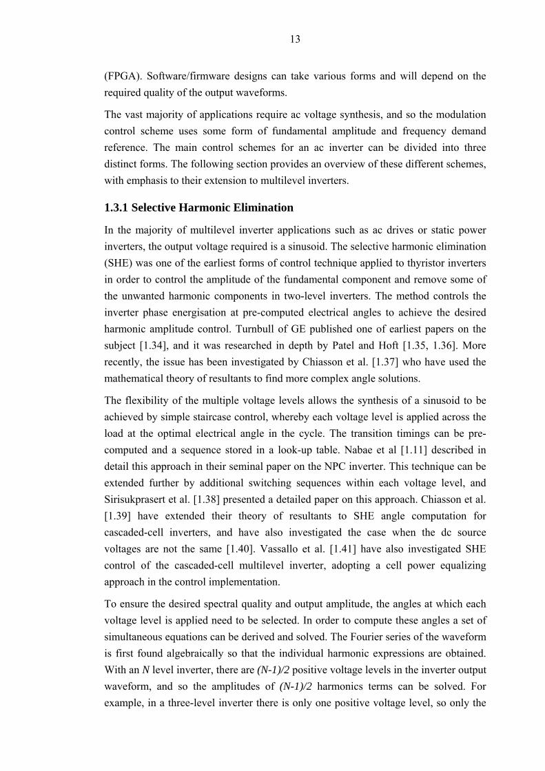
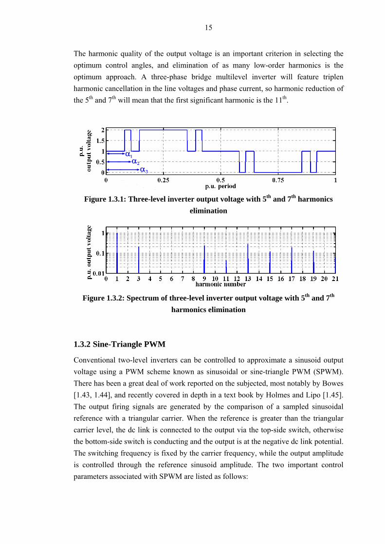
For example, the SHE control method can be applied to a three-level inverter, to regulate the fundamental and eliminate two unwanted harmonics; the 5th and 7th. Figure 1.3.1 illustrates the normalised output voltage waveform and Figure 1.3.2 the output harmonic spectrum. To compute the angles, (1.3.1) and (1.3.2) are used to get a set of three simultaneous equations,
11 1 2 3cos( ) cos( ) cos( )
4 level
VbVπα α α= − + = … (1.3.3)
5 1 2 3cos(5 ) cos(5 ) cos(5 ) 0b α α α= − + = … (1.3.4)
7 1 2 3cos(7 ) cos(7 ) cos(7 ) 0b α α α= − + = … (1.3.5)
The required firing angles can then be computed using the Newton-Raphson method for nonlinear systems of equations [1.42]. The method uses the first two terms of the Taylor series expansion of a function f(x), and an iterative process used to approach the root of the function, using the formula,
( )( )1 'n n
f xx x
f x+ = − … (1.3.6)
The method then requires the partial derivative of (1.3.1) for each angle to be solved and has the form,
4 sinn dcm
m
b V nN
αα π∂
= −∂
… (1.3.7)
15
The harmonic quality of the output voltage is an important criterion in selecting the optimum control angles, and elimination of as many low-order harmonics is the optimum approach. A three-phase bridge multilevel inverter will feature triplen harmonic cancellation in the line voltages and phase current, so harmonic reduction of the 5th and 7th will mean that the first significant harmonic is the 11th.
Figure 1.3.1: Three-level inverter output voltage with 5th and 7th harmonics elimination
Figure 1.3.2: Spectrum of three-level inverter output voltage with 5th and 7th harmonics elimination
1.3.2 Sine-Triangle PWM
Conventional two-level inverters can be controlled to approximate a sinusoid output voltage using a PWM scheme known as sinusoidal or sine-triangle PWM (SPWM). There has been a great deal of work reported on the subjected, most notably by Bowes [1.43, 1.44], and recently covered in depth in a text book by Holmes and Lipo [1.45]. The output firing signals are generated by the comparison of a sampled sinusoidal reference with a triangular carrier. When the reference is greater than the triangular carrier level, the dc link is connected to the output via the top-side switch, otherwise the bottom-side switch is conducting and the output is at the negative dc link potential. The switching frequency is fixed by the carrier frequency, while the output amplitude is controlled through the reference sinusoid amplitude. The two important control parameters associated with SPWM are listed as follows:
16
ma – amplitude modulation index (ratio of reference peak-to-peak to dc link voltage)
mf – frequency modulation index (ratio of carrier frequency to reference frequency)
In a multilevel inverter, the basic building block of an SPWM controller can be applied to produce a number of different multilevel PWM control strategies, each offering slightly different performance characteristics when applied to a multilevel inverter topology. All the control schemes use one reference sinusoid and a separate carrier for each pair of power switches associated with a voltage level. In a digital implementation carrier redundancy can be exploited to reduce the amount hardware resources required.
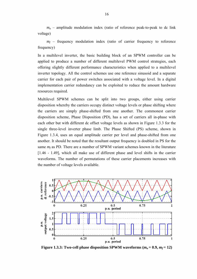
Multilevel SPWM schemes can be split into two groups, either using carrier disposition whereby the carriers occupy distinct voltage levels or phase shifting where the carriers are simply phase-shifted from one another. The commonest carrier disposition scheme, Phase Disposition (PD), has a set of carriers all in-phase with each other but with different dc offset voltage levels as shown in Figure 1.3.3 for the single three-level inverter phase limb. The Phase Shifted (PS) scheme, shown in Figure 1.3.4, uses an equal amplitude carrier per level and phase-shifted from one another. It should be noted that the resultant output frequency is doubled in PS for the same mf as PD. There are a number of SPWM variant schemes known in the literature [1.46 - 1.49], which all make use of different phase and level shifts in the carrier waveforms. The number of permutations of these carrier placements increases with the number of voltage levels available.
Figure 1.3.3: Two-cell phase disposition SPWM waveforms (ma = 0.9, mf = 12)

17
Figure 1.3.4: Two-cell phase shifted SPWM waveforms (ma = 0.9, mf = 12)
Modern digital implementations of SPWM entail sampling of the modulation scheme waveforms. Macro sampling can be applied to the reference where the value only changes at the start of carrier triangle (symmetric sampling) or at both peak and trough (asymmetric sampling). Micro sampling effects are present due to the digital controller’s clock frequency and possible lower internal sampling rates caused by interrupt servicing, computational latency, etc. These sampling effects, together with the dead-times introduced in the firing signals to avoid shoot-through failures, all influence the performance of the inverter.
1.3.3 Space Vector PWM
The space vector PWM (SVPWM) technique is an important alternative means of generating the switching pattern for a three-phase voltage-source inverter. Mapping of the three-phase stationary reference frame voltage states in the inverter to an orthogonal reference frame using the Clarke transform, allows the duty cycles for each phase to be computed relatively simply. The SVPWM method was first described for controlling NPC inverters in the 1980s [1.50, 1.51].
The Clarke transform is applied to an arbitrary set of balanced three-phase voltages to obtain the so called space vector representation in the complex α-β plane. The time-dependent vector, V, is derived from the individual phase-to-neutral voltages according to the relationship.
2 43 32
3j j
an bn cnv v e v eπ π⎛ ⎞
= + +⎜ ⎟⎝ ⎠
V … (1.3.8)
where van, vbn and vcn are the stationary node voltages with respect to the centre-point neutral of a balanced three-phase load, and the following relationship holds:

18
0 … (1.3.9) an bn cnv v v+ + =
The space vector diagram of the eight voltage states in a three-phase inverter is shown in Figure 1.3.5. The triangular sector in which the target reference vector lies is first identified and then the duty cycles for the boundary vectors are computed, giving the upper switch on-time for each phase. The two zero sequence vectors [000] and [111] are conventionally used in equal measure to complete the total switching period, and the resultant switching pattern is arranged symmetrically as shown in Figure 1.3.6. The popularity of the space vector scheme is due to its relatively low harmonic distortion and inherent increased modulation depths (ma > 1). Nowadays, commercial microcontrollers and DSPs aimed at power electronics and motion control applications have dedicated hardware implementations which simplify the use of SVPWM in conventional two-level inverter applications.
Figure 1.3.5: Space vector diagram for a conventional two-level inverter
Figure 1.3.6: Symmetric firing pattern of the SVPWM scheme

19
When the space vector concept is extended to multilevel inverters there are an increased number of space vectors in the orthogonal reference plane. Figure 1.3.7 illustrates the space vector diagram for a three-phase, five-level inverter. The vector number indicates the output voltage level for each phase. This means that there is an increase in the vector options available for synthesising the reference, and this increases the complexity of the computational algorithm required to exploit the performance of the SVPWM control scheme. The problem of optimum selection of the switching state space vectors has intrigued researchers and there have been various optimum solutions reported on the issue, notably Lee et al. [1.52] and Wei at al. [1.53]. The optimum vector selection can also improve other performance criteria such as the common voltage ripple as reported by Zhang et al. [1.54].
Figure 1.3.7: Space vector diagram for two-cell, three-level inverter
1.3.4 Hysteretic Current Control
Current-regulated control can also be employed in order to maintain the output current within a small hysteresis band. The control can employ multiple hysteresis bands for identifying the required output voltage level such as the method described by Marchesoni [1.55] and Corzine [1.56]. Alternative schemes have also been proposed such as a voltage level selection based on the derivative current error by Bode et al. [1.57].
20
Hysteretic current control is suitable in motor drive systems where a high bandwidth is required, but can only be used when the rate of change of phase current for a given applied voltage allows a realistic range of inverter switching frequencies. The main disadvantage is the variable switching frequency that results and in so hysteretic current control is not generally favoured in most mainstream applications.
1.4 Multilevel Converter Applications
1.4.1 Forms of Power Conversion
The multilevel converter circuits can be applied to all four canonical power converter forms. Their applications can be briefly categorised as follows:
• Rectification: The diode-clamped and flying-capacitor bridge topologies are suitable for use as an active front-end (AFE) for interfacing between an ac source and a system dc link. Rectification can be performed simply by control of the switches and additional benefits of low harmonic current distortion and power factor improvements can be realised. Additional regulation of the dc link can be done and a multilevel AFE will allow regenerative power in a drive system to be supplied back to the ac source. It is also possible to use a cascaded-cell inverter coupled via a transformer to an ac source as a rectifier.
• Inversion: This is the primary application for a multilevel converter circuit, where the source voltage is dc and the load is ac. All multilevel circuits can operate as inverters, but in the case of the cascaded-cell circuit, there are multiple voltage sources.
• DC/DC Conversion: The diode-clamped and flying-capacitor means of protecting the peak voltages across the power switches can be applied in a chopper circuit configuration. The flying-capacitor circuit was originally conceived for use as a multilevel chopper. In dc power supplies, boosting or bucking modes of control can be used.
• AC/AC Conversion: Unlike the matrix converter there is no direct ac to ac conversion mode available inherently in the multilevel configurations, since they use internal dc sources to protect the individual power switches. However, by combining a multilevel AFE and a multilevel inverter in an intertie configuration, connections between different ac systems can be achieved with bidirectional power flow.
21
1.4.2 Medium Voltage Drive Systems
Traditionally, medium voltage drive systems have used thyristor-based current source inverters because of the lack of available high power forced commutated electronic switches. The advent of the GTO has now shifted the balance towards voltage source inverters and large drive systems are now benefiting from improvements in performance gained from variable speed [1.58]. Multilevel inverter technology has provided even more scope for operating large drives in variable speed, since the main benefit is the improved harmonic quality and reduced switching loss [1.59]. A multilevel inverter has the benefit of operating at higher voltages with fast switching frequencies, so that the output voltage quality is sufficiently good to avoid large additional filtering. This is important with relation to cost and overall drive size.
The original NPC (three-level diode clamped inverter) was originally envisaged for drive applications and indeed it is now used extensively in higher power, medium voltage drive systems [1.60]. The cascaded-cell inverter has also found application in very high power drive systems such as gas pipeline compressors [1.61]. The flying-capacitor inverter has also been commercialised by Alstom for drive system applications [1.62].
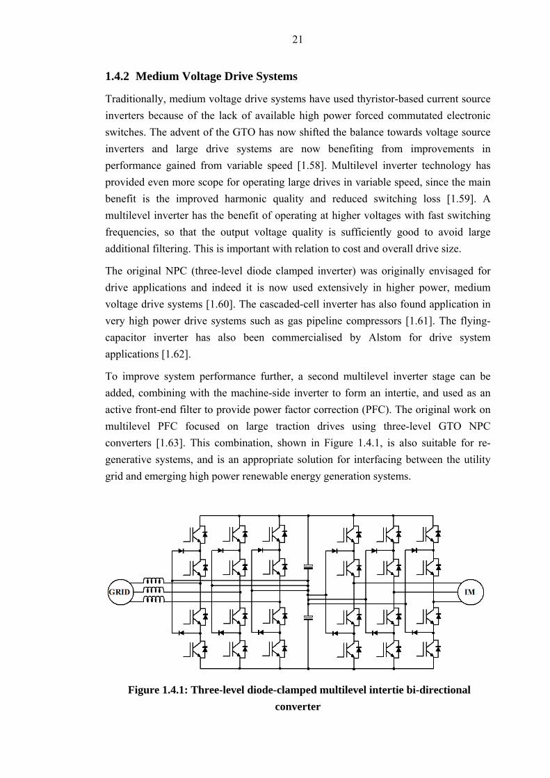
To improve system performance further, a second multilevel inverter stage can be added, combining with the machine-side inverter to form an intertie, and used as an active front-end filter to provide power factor correction (PFC). The original work on multilevel PFC focused on large traction drives using three-level GTO NPC converters [1.63]. This combination, shown in Figure 1.4.1, is also suitable for re-generative systems, and is an appropriate solution for interfacing between the utility grid and emerging high power renewable energy generation systems.
Figure 1.4.1: Three-level diode-clamped multilevel intertie bi-directional converter

22
1.4.3 Power Conditioning
The concept of a flexible ac transmission system (FACTS) provides opportunities for a number of different applications of multilevel converter circuits to be connected within a power distribution system [1.64], and through control help to improve the overall power quality and system performance.
Decoupled voltage source inverter circuits are used as static VAr compensators (STATCOM), and the benefits of the multilevel inverter make them attractive in higher voltage systems [1.65 - 1.68]. Figure 1.4.2 shows a shunt-connected three-phase inverter in an ac transmission system. The inverter is rated to supply only reactive power at the point of load, thus through optimum control compensate for poor load power factors. This reduces the level of current being supplied by the utility grid and maximises the overall system power delivery capacity.
Figure 1.4.2: Shunt-connected multilevel inverter arrangement
Active filtering is also possible with this shunt arrangement where more advanced control of the multilevel inverter can also remove unwanted harmonics from flowing in the transmission system, reducing the requirement for large passive filtering. This is done by controlling the injection of anti-phase current harmonic components which cancel those present in the load current.
Active filtering can also be achieved by series connecting the multilevel inverter via transformers as shown in Figure 1.4.3. This arrangement can de-couple the unwanted load harmonics from the transmission side, and additionally be used for maintaining the load voltage during short lived supply voltage disturbances.

23
Figure 1.4.3: Series-connected multilevel inverter arrangement
The shunt and series connected multilevel inverters can be combined in the form of an intertie to provide a power quality solution known variously as unified power flow controller (UPFC) or universal power line conditioner (UPLC) [1.69]. The series circuit compensates for source-side harmonics and voltage disturbances, while the shunt circuit deals with load dependent power quality issues.
These system concepts will become increasingly important as more distributed generation networks evolve using combinations of different localised power generation. By replacing the dc link capacitors in a shunt-connected multilevel inverter with a source of dc power such as fuel cells, batteries or other energy storage system the circuit acts as an uninterruptible power supply, providing load power for longer periods of power outage. Extending the concept further, using renewable sources of energy such as photovoltaic and wind turbines, the multilevel inverter system becomes an integral part of a supply generator in a distributed supply network.
1.5 Challenges and Practical Issues
The first challenge faced in developing a multilevel inverter solution for a specific application is selecting from wide variety of circuit topologies, numbers of voltage levels and different modulation control schemes available. There is no definitive answer as to what topology is best for an application. The different circuit topologies contain different numbers of the core constituent components. A comparison can be

24
drawn by comparing the major component requirements for a nine-level, three-phase inverter when used as a grid-connected shunt active filter. Table 1.5.1 lists the number of different components required in each case. It is assumed that all components are of equal voltage rating so the numbers of clamping capacitors and diodes reflects this.
Diode-Clamped Flying-Capacitor Cascaded-Cell Transistors 24 24 24 Diodes 60 24 24 Capacitors 4 18 12
Table 1.5.1: Comparison of the number of main power components
Not surprisingly, the diode-clamped has the largest silicon content with the lowest number of capacitors whilst the flying-capacitor inverter has the most capacitors. The cascaded-cell inverter uses the least number of components but requires smoothing capacitors for each cell which see a significant twice line frequency ripple current. The final decision has to be made by assessing the actual application requirements in terms of power rating and performance, in light of the available rated components to achieve the end goal.
The selection of level number again can only be decided commercially, because of the increasing circuit complexity versus better performance offered as the number of levels increases. The judgement, however, will be dictated by the available power switch technology. Advances in semiconductors are pushing the upper limits of operating breakdown voltage and reducing the switching energy loss characteristic thus increasing the potential operating frequencies of the inverter. Wide band-gap semiconductors may also play a defining role in future developments if the potential promise of these devices is realisable commercially.
Once the best topology has been identified, then the optimum control of the inverter is a major challenge faced by the system designer. Voltage modulation of the fundamental frequency component in ac systems is relatively straightforward and can be achieved easily with modern microelectronics. However, the specific topological requirements for maintaining balanced system operation in terms of equal power loss distribution in all the power electronic switches and ensuring that capacitor voltages are at the required levels is a major issue. Selecting the type of control scheme and operating frequency needs careful thought, since it has a bearing on the size of the energy storage devices and losses in the inverter system.

25
Of most significance in all multilevel inverter applications is the minimisation of the unwanted harmonic components in the output voltage and/or current. Certain control schemes may offer improved harmonic distortion over other methods, and these issues need to be appraised thoroughly in light of the application and any legislative requirements. Increasing the available output voltage levels can play an important role in reducing the harmonic distortion and operating frequency and will have a bearing on the extra cost and size of passive filtering components. In drive systems, where the load is inductive, the phase current waveforms will be well filtered, but the control scheme must avoid introducing harmonic components which lead to significant torque perturbations at the motor shaft.
Individual drive systems may require different levels of acceptable harmonic distortion. In the case of grid-connection there are a number of international standards setting-out acceptable levels of total harmonic distortion, and allowable levels for individual harmonics of the fundamental. The most notable are IEC EN61000-3-2 [1.70] and IEEE 519-1992 [1.71]. Table 1.5.2 lists the maximum recommended amplitude of the odd current harmonics as a percentage of the supplied fundamental current in distribution systems up to 69 kV as recommended in IEEE519. The total harmonic distortion is recommended to be less than 5%. The even harmonics area limited to 25% of the odd harmonics in the specified range. These levels are for systems where the maximum load current is greater than a 20th of the maximum inverter rating.
Harmonic n < 11 11 ≤ n < 17 17 ≤ n < 23 23 ≤ n < 35 35 ≤ n THD
Limit 4% 2% 1.5% 0.6% 0.3% 5% Table 1.5.2: Maximum harmonic current as percentage of fundamental current
The maximum amplitudes specified in the table have also been incorporated into new IEEE 1547 standards regarding the interconnection of distributed power sources [1.72]. This standard is applicable to inverters for renewable energy sources such as wind, solar panels and fuel-cells.
1.6 Motivation and Objectives
The diode-clamped and cascaded-cell inverters are far more mature technologies commercially. This is partly due to intellectual property rights issues, but can also be understood when comparing the number of capacitor storage elements required, compared to the flying-capacitor circuit. There has been much academic interest in
26
multilevel control schemes which can be applied to all forms of multilevel inverter. Most work has focussed on specific control techniques and generally assumed the inverter has ideal behaviour with perfect voltage level synthesis. When investigations on system balancing have been undertaken, the effects on output power quality have largely been ignored.
The challenge in getting the flying-capacitor inverter accepted as a suitable alternative for most high power applications is to minimise the total cost of the capacitor storage elements, while maintaining high reliability and excellent power quality performance. Therefore, the focus of this investigation is to identify optimal control techniques in conjunction with system voltage balancing algorithms, and quantify the capacitor sizing against the desired operating parameters.
The main analysis tool for the investigation is a specially developed computer simulation program which incorporates the key characteristics of the overall system’s components, so that accurate predictions of behaviour of a real inverter can be assessed. Control optimisation is assessed through experimental work on a four-cell, five-level inverter, and measurements used to verify the validity of the conclusions reached through simulation.
The thesis is divided into the following major chapters:
Chapter 1:
Introduction chapter on multilevel topologies in general, their basic characteristics and major applications with reference to the present state of the art as published in the literature. The practical problems associated with implementation so setting out the motivation and objectives of the research conducted specifically on the flying-capacitor inverter topology.
Chapter 2:
This chapter focuses specifically on the flying-capacitor inverter’s characteristics, especially the issue of internal inverter balancing. The existing literature on the topology is reviewed thoroughly and major issues in its implementation highlighted. The complexity of the inverter operating modes is analysed in detail and the requirements for cell-capacitor voltage balancing are identified. Basic circuit models are introduced and a more detailed simulator, developed specifically for the work, is described.
Chapter 3:
Selective harmonic elimination (SHE) control as applied to a flying-capacitor inverter is covered in this chapter. The important issue of system balancing, introduced in Chapter 2, is addressed in the context of the simplest form of SHE,

27
staircase output voltage operation. An important contribution is made through a systematic method of selecting optimum balancing patterns and it is shown that reductions in harmonic distortion can be achieved when applied to inverters with practical sized cell-capacitors. Simulation is used throughout the chapter to support the analysis.
Chapter 4:
Sine-triangle PWM is dealt with in detail in this chapter, using simulation to analyse the system operation under different carrier placement PWM implementations. The performance of the different PWM schemes is compared, including the influence of practical sized inverter components, and digital controller implementation aspects. A novel digital hardware design of a cell-capacitor voltage balancing approach is presented which is applicable to all forms of PWM control.
Chapter 5:
This chapter repeats the analysis of the inverter when controlled using space vector PWM, and introduces a simplified implementation approach for multilevel inverters. Comparisons are drawn between space vector PWM and sinusoidal PWM, specifically third-harmonic injection.
Chapter 6:
A practical multilevel inverter designed and built for laboratory experimentation is described in this chapter. Results of operation under a variety of different control schemes are used to support the validity of the previous chapters’ simulation analysis.
Chapter 7:
The concluding chapter with a review of the major achievements of the work and recommendations on future research work.
1.7 References
[1.1] Mohan, N., Undeland, T.M. and Robbins, W.P., “Power electronics. Converters, applications, and design”, John Wiley & Sons, Inc., New York, USA, 3rd Edition, 2003.
[1.2] Akagi, H., "Trends in power electronics and motor drives", Proceedings of PEDS 2003, the 5th International Conference on Power Electronics and Drive Systems, 17 - 20 November, 2003, Vol. 1, pp. 1 - 7.

28
[1.3] Lorenz, L., "New power semiconductor components for future innovative high frequency power converters", Proceedings of ICIT 2003, IEEE International Conference on Industrial Technology, 10 - 12 December, 2003, Vol. 2, pp. 1173 - 1177.
[1.4] Chittat, V., Hongt, S. and Torrey, D.A., "Series Connection of IGBTs with Active Voltage Balancing", Conference Record of IAS '97, 32nd Industry Applications Society Annual Meeting, 5 - 9 October, 1997, Vol. 2, pp. 961 - 967.
[1.5] Special Section on Multilevel Inverters – I, IEEE Transactions on Industrial Electronics, Vol. 49, No. 4, August 2002, pp. 722 – 888.
[1.6] Special Section on Multilevel Inverters – II, IEEE Transactions on Industrial Electronics, Vol. 49, No. 5, October 2002, pp. 946 – 1100.
[1.7] Lai, J.-S. and Peng, F.Z., “Multilevel converters - a new breed of power converters”, Conference Record of IAS '95, the IEEE Industry Applications Society 30th Annual Meeting, 8 - 12 October, 1995, Vol. 3, pp. 2348 – 2356.
[1.8] Teodorescu, R., Blaabjerg, F., Pedersen, J.K., Cengelci, E.,. Sulistijo, S.U, Woo, B.W. and Enjeti, P., “Multilevel converters - a survey”, Proceedings of EPE '99, 8th European Conference on Power Electronics and Applications, 7 - 9 September 1999, CD-ROM paper.
[1.9] Baker, R.H., “High-voltage converter circuit”, US Patent No. US4203151, Filed 21st September, 1978, Granted 13th May, 1980.
[1.10] Baker, R.H., “Bridge converter circuit”, US Patent No. US4270163, Priority Filed 12th September 1978, Granted 26th May, 1981.
[1.11] Nabae, A., Takahashi, J. and Akagi, H., "A new neutral-point-clamped PWM inverter", Proceedings of IAS '80, the IEEE Industry Applications Society Annual Meeting, 29 November – 3 October 1980, pp 761 - 766.
[1.12] Andrejak, J.M. and Lescure, M., “High voltage converters promising technological developments”, Proceedings of EPE '87, 2nd European Conference on Power Electronics and Applications, 22 - 24 September, 1987, pp. 1.159 – 1.162.
[1.13] Choi, N.S., Cho, J.G. and Cho, G.H., “A general circuit topology of multilevel inverter”, PESC '91 Record. 22nd Annual IEEE Power Electronics Specialists Conference, 24 - 27 June, 1991, pp 96 – 103.

29
[1.14] Carpita, M. and Tenconi, S., “A novel multilevel structure for voltage source inverter”, Proceedings of EPE '91, 4th European Conference on Power Electronics and Applications, 3 - 6 September 1991, pp. 1.90 – 1.94.
[1.15] Peng, F.Z., Lai, J.S. and McKeever, J., “A multilevel voltage-source converter system with balanced dc voltages”, PESC '95 Record. 26th Annual IEEE Power Electronics Specialists Conference, 18 - 22 June, 1995, pp. 1144 – 1150.
[1.16] Simon, E.D. and Bonner, G., "An inductive energy storage system using Ignitron switching", IEEE Transactions on Nuclear Science, Vol. NS-14, No. 5, 1967.
[1.17] Dickerson, J.A. and Ottaway, G.H., “Transformerless power supply with line to load isolation”, US Patent No. 3596369, Filed 22 December 1969.
[1.18] Singer, Z., Emanuel, A. and Erlicki, M.S., "Power regulation by means of a switched capacitor", Proceedings of the IEE, Vol. 119, No. 2, February 1972, pp. 149 - 152.
[1.19] Meynard, T.A. and Foch, H., "Dipositif électronique de conversion d'énergie électrique", French Patent No. 2679715B1, Filed 25th July 1991, Issued 29th January 1993.
[1.20] Meynard, T.A. and Foch, H., “Multi-level choppers for high voltage applications”, EPE Journal, Vol. 2, No. 1, March 1992, pp. 45 – 50.
[1.21] Marchesoni, M., Mazzucchelli, M. and Tenconi, S., “A non conventional power converter for plasma stabilization”, PESC '88 Record, 19th Annual IEEE Power Electronics Specialists Conference, 11 - 14 April 1988, Vol. 1, pp. 122 – 129.
[1.22] Hammond, P.W., “Medium voltage PWM drive and method”, US Patent No. 5625545, Filed 1st March 1994, Issued 29th April 1997.
[1.23] Hammond, P.W., “A new approach to enhance power quality for medium voltage drives”, Record of the IEEE Industry Applications Society 42nd Annual Petroleum and Chemical Industry Conference, 11 - 13 September 1995, pp. 231 – 235.
[1.24] Kumar, M.R.P. and Kim, J.M.S., “Current control of a hybrid multilevel switching converter”, Proceedings of PEDES '96, the 1st IEEE International Conference on Power Electronics, Drives and Energy Systems for Industrial Growth, 8 - 11 January, 1996, Vol. 1, pp. 346 - 352.
30
[1.25] Peng, F.Z., “A generalized multilevel inverter topology with self voltage balancing”, Conference Record of IAS 2000, the 2000 IEEE Industry Applications Society 35th Annual Meeting, 8 - 12 October, 2000, Vol. 3, pp. 2024 – 2031.
[1.26] Bhagwat, P.M. and Stefanovic, V.R., “Generalized structure of a multilevel PWM inverter”, IEEE Transactions on Industry Applications, Vol. IA-19, No. 6, November/December 1983, pp. 1057 – 1069.
[1.27] Manjrekar, M.D., Steimer, P.K. and Lipo, T.A., “A hybrid multilevel inverter topology for drive applications”, Proceedings of APEC '98, IEEE 13th Annual Applied Power Electronics Conference and Exposition, 16 - 19 February, 1998, Vol. 2, pp. 523 - 529.
[1.28] McGrath, B.P., Holmes, D.G., Manjrekar, M. and Lipo, T.A., “An improved modulation strategy for a hybrid multilevel inverter”, Conference Record of IAS 2000, the 2000 IEEE Industry Applications Society 35th Annual Meeting, 8 - 12 October, 2000, Vol. 4, pp. 2086 – 2093.
[1.29] Flairty, C.W., “A 50 kVA adjustable-frequency 23-phase controlled rectifier inverter”, AIEE Industrial Electronics Symposium, 20 -21 September, 1961.
[1.30] Cengelci, E., Woo, B.W., Enjeti, P., Teodorescu, R. and Blaabjerg, F., "A new medium voltage PWM inverter topology for adjustable speed drives", IEEE Transactions on Industry Applications, Vol. 35, No. 3 May/June 1999, pp. 628-637.
[1.31] Schienbein, L.A., Droppo, G.W., Donnelly, M.K. and Harris, B.E., “Step wave power converter”, US Patent No. US6198178B1, Filed 21st December 1999, Granted 6th March 2001.
[1.32] Kang, F.-S., Park, S.-J. and Kim, C.-U., “Multilevel inverter employing cascaded transformers”, Proceedings of IECON ’03, 29th Annual Conference of the IEEE Industrial Electronics Society, 2 – 6 November, 2003, Vol. 3, pp. 2169 – 2174.
[1.33] Shakweh, Y., “MV inverter stack topologies”, IEE Power Engineering Journal, June 2001, pp. 139 – 149.
[1.34] Turnbull, F.G., “Selected harmonic reduction in static d-c – a-c inverters”, IEEE Transactions on Communications and Electronics, Vol. 83, July 1964, pp. 374 – 378.
[1.35] Patel, H.S. and Hoft, R.G. “Generalized harmonic elimination and voltage control in thyristor inverters – Part I – Harmonic elimination”, IEEE
31
Transactions on Industry Applications, Vol. IE-9, May/June 1973, pp. 310 – 317.
[1.36] Patel, H.S. and Hoft, R.G. “Generalized harmonic elimination and voltage control in thyristor inverters – Part II – Voltage control technique”, IEEE Transactions on Industry Applications, Vol. IE-10, September/October 1974, pp. 666 - 673.
[1.37] Chiasson, J.N., Tolbert, L.M., McKenzie, K.J. and Du, Z., “A complete solution to the harmonic elimination problem”, IEEE Transactions on Power Electronics, Vol. 19, No. 2, March 2004, pp. 491 – 499.
[1.38] Sirisukprasert, S., Lai, J.-S. and Liu, T.-H., “Optimum harmonic reduction with a wide range of modulation indexes for multilevel converters”, Conference Record of IAS 2000, the IEEE Industry Applications Society 35th Annual Meeting, 8 - 12 October, 2000, Vol. 3, pp 2094 – 2099.
[1.39] Chiasson, J.N., Tolbert, L.M., McKenzie, K.J. and Du, Z., “A unified approach to solving the harmonic elimination equations in multilevel converters”, IEEE Transactions on Power Electronics, Vol. 19, No. 2, March 2004, pp. 478 – 490.
[1.40] Tolbert, L.M., Chaisson, J.N., McKenzie, K.J. and Du, Z., “Elimination of harmonics in a multilevel converter with non equal DC sources”, Proceedings of APEC ’03, the 18th Annual IEEE Applied Power Electronics Conference and Exposition, 9 – 13 February, 2003, Vol. 1, pp. 589 – 595.
[1.41] Vassallo, J., Clare, J.C. and Wheeler, P.W., “A power-equalized harmonic-elimination scheme for utility-connected cascaded H-bridge multilevel converters”, Proceedings of IECON ’03, 29th Annual Conference of the IEEE Industrial Electronics Society, 2 – 6 November, 2003, Vol. 2, pp. 1185 – 1190.
[1.42] Press, W.H., Flannery, B.P., Teukolsky, S.A. and Vetterling, W.T., “Numerical recipes in C. The art of scientific computing”, Cambridge University Press, 1988, ISBN 0-521-35465-X, Chapter 9, pp. 270 – 275.
[1.43] Bowes, S.R., “New sinusoidal pulsewidth-modulated inverter”, IEE Proceedings, Vol. 122, No. 11, November, 1975, pp. 1279 - 1285.
[1.44] Bowes, S.R. and Mount, M.J., “Microprocessor control of PWM inverters”, IEE Proceedings, Vol. 128, Part B, No. 6, November 1981, pp. 293 – 305.
[1.45] Holmes, D.G. and Lipo, T.A., “Pulse width modulation for power converters. Principles and practice”, Wiley-IEEE Press Series on Power Engineering, 2003, ISBN 0-471-20814-0.

32
[1.46] Tolbert, L.M. and Habetler, T.G., “Novel multilevel inverter carrier-based PWM methods”, Conference Record of IAS '98, the 1998 IEEE Industry Applications Society 33rd Annual Meeting, 12 - 15 October, 1998, Vol. 2, pp. 1424 – 1431.
[1.47] Agelidis, V.G. and Calais, M., "Application specific harmonic performance evaluation of multicarrier PWM techniques", PESC '98 Record, 29th Annual IEEE Power Electronics Specialists Conference, 17 - 22 May, 1998, Vol. 1, pp 172 - 178.
[1.48] McGrath, B.P. and Holmes, D.G., “A comparison of multicarrier PWM strategies for cascaded and neutral point clamped multilevel inverters”, Proceedings of PESC 2000, 31st Annual IEEE Power Electronics Specialists Conference, 18 - 23 June, 2000, Vol. 2, pp. 674 – 679.
[1.49] Massoud, A.M., Finney, S.J. and Williams, B.W., “Control techniques for multilevel voltage source inverters”, Proceedings of PESC '03, 34th IEEE Power Electronics Specialists Conference, 15 - 19 June, 2003, Vol. 1, pp. 171 – 176.
[1.50] Steinke, J.K., "Control strategy for a three phase AC traction drive with three-level GTO PWM inverter", Proceedings of PESC '88, 19th Annual IEEE Power Electronics Specialists Conference, 11-14 April 1988, Vol. 1, pp. 431 - 438.
[1.51] Bauer, F. and Heining, H.-D., “Quick response space vector control for a high power three-level inverter drive system”, Proceedings of EPE ’89, the 3rd European Conference on Power Electronics and Applications, 9 – 12 October, 1989, Vol. 1, pp. 417 – 421.
[1.52] Lee, Y.-H., Kim, R.-Y. and Hyun, D.-S., “A novel SVPWM strategy considering DC-link balancing for a multi-level voltage source inverter”, Proceedings of APEC '99, the 14th IEEE Applied Power Electronics Conference and Exposition, 14 - 18 March, 1999, Vol. 1, pp. 509 – 514.
[1.53] Wei, S.-M., Wu, B., Li, F.-H. and Liu, C.-W., "A general space vector PWM control algorithm for multilevel inverters", Proceedings of APEC '03, the 18th IEEE Applied Power Electronics Conference and Exposition, 9 - 13 February, 2003, Vol. 1, pp. 562 - 568.
[1.54] Zhang. H.-R., von Jouanne, A. and Wallace, A. "Multilevel inverter modulation schemes to eliminate common-mode voltages", Conference Record of IAS '98, the 33rd IEEE Industry Applications Annual Meeting, 12 - 15 October, 1998, Vol. 1, pp. 752-758.

33
[1.55] Marchesoni, M., "High performance current control techniques for applications to multilevel high power voltage source inverters", Proceedings of PESC '89, the 20th IEEE Power Electronics Specialists Conference, 26 - 29 June, 1989, Vol. 2, pp. 672 - 682.
[1.56] Corzine, K.A., “A hysteresis current-regulated control for multi-level drives”, IEEE Transactions on Energy Conversion, Vol. 15, No. 2, June 2000, pp. 169 – 175.
[1.57] Bode, G.H., Zmood, D.N., Loh, P.C. and Holmes, D.G., “A novel hysteresis current controller for multilevel single phase voltage source inverters”, Proceedings of PESC 2000, 31st Annual IEEE Power Electronics Specialists Conference, 18 - 23 June, 2000, Vol. 4, pp. 1845 – 1850.
[1.58] Marchesoni, M. and Mazzucchelli, M., "Multilevel converters for high power AC drives: a review", Proceedings of ISIE '93, IEEE International Symposium on Industrial Electronics, 1 - 3 June, 1993, pp. 38 - 43.
[1.59] Newton, C. and Summer, M., “Multi-level convertors a real solution to medium/high-voltage drives?”, IEE Power Engineering Journal, Vol. 12, No. 1, February 1998, pp. 21 – 26.
[1.60] Tamai, S., Koyama, M., Fujii, T., Mizoguchi, S. and Kawabata, T., “3 level GTO converter-inverter pair system for large capacity induction motor drive”, Proceedings of EPE '93, 5th European Conference on Power Electronics and Applications, IEE Conference Publication No. 377, 13 - 16 September, 1993, Vol. 5, pp. 45 – 50.
[1.61] Hammond, P.W., “Enhancing the reliability of modular medium-voltage drives”, IEEE Transactions on Industrial Electronics, Vol. 49, No. 5, October 2002, pp. 948 – 954.
[1.62] Beinhold, G., Jakob, R. and Nahrstaedt, M., “A new range of medium voltage multilevel inverter drives with floating capacitor technology”, Proceedings of EPE '01, 9th European Conference on Power Electronics and Applications, 27 - 29 August, 2001, CDROM Paper No. PP00426.
[1.63] Ghiara, T., Marchesoni, M. and Sciutto, G., "High power factor control system in multilevel converters for AC heavy traction drives", Proceedings of APEC '90, the 5th IEEE Applied Power Electronics Conference and Exposition, 11-16 March 1990, pp. 672 - 680.
[1.64] Gyugyi, L., "Application characteristics of converter-based FACTS controllers", Proceedings of PowerCon 2000, the International Conference on Power System Technology, 4 - 7 December, 2000, Vol. 1, pp. 391 - 396.

34
[1.65] Choi, N.S., Cho, G.C. and Cho, G.H., "Modeling and analysis of a static VAR compensator using multilevel voltage source inverter", Conference Record of IAS '93, the 1993 IEEE Industry Applications Society 28th Annual Meeting, 2 - 8 October, 1993, Vol. 2, pp. 901 - 908.
[1.66] Peng, P.Z. and Lai, J.S., “A static VAr generator using a staircase waveform multilevel voltage source converter”, Proceedings of PCIM/PQ '94, the Power Quality Conference, 17 - 22 September, 1994, pp. 58 – 66.
[1.67] Liang, Y. and Nwankpa, C.O., “New type of STATCOM based on cascading voltage source inverters with phase-shifted unipolar SPWM”, Conference Record of IAS '98, the 1998 IEEE Industry Applications Society 33rd Annual Meeting, 12 - 15 October, 1998, Vol. 2, pp. 1447 – 1453.
[1.68] Min, W., Min, J. and Choi. J., “Control of STATCOM using cascade multilevel inverter for high power application”, Proceedings of PEDS '99, 3rd International Conference on Power Electronics and Drive Systems, 27 - 29 July, 1999, Vol. 2, pp 871 – 876.
[1.69] Tolbert, L.M.; Peng, F.Z.; Habetler, T.G., "A multilevel converter-based universal power conditioner", Proceedings of PESC '99, 30th IEEE Power Electronics Specialists Conference, 27 June-1 July 1999, Vol. 1, pp. 393 - 399.
[1.70] IEC Standard EN61000-3-2, “Electromagnetic compatibility (EMC) part 3: Limits – section 2: Limits for harmonic current emissions (equipment input current <= 16A per phase)”, 15th March, 2001.
[1.71] IEEE Std. 519-1992, “IEEE recommended practices and requirements for harmonic control in electrical power systems”. IEEE Inc., USA, 12 April 1993.
[1.72] IEEE Std. 1547-2003, “IEEE standard for interconnecting distributed resources with electric power systems”, IEEE Inc., USA, 26th July, 2003.