Defect Engineering During Czochralski Crystal Growth and Silicon Wafer Manufacturing
Upload
allison-meltonCategory
view
235download
6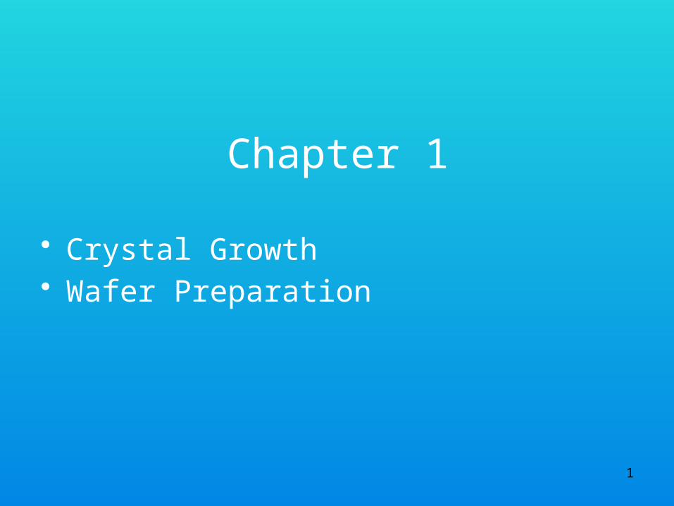
Chapter 1
• Crystal Growth• Wafer Preparation
1
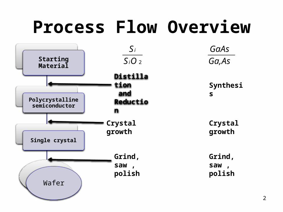
Process Flow Overview
Starting Material
Polycrystalline semiconductor
Single crystal
Wafer
2OS
S
i
i
Ga,As
GaAs
Distillation andReduction
Crystal growth
Grind, saw , polish
Synthesis
Crystal growth
Grind, saw , polish
2
Overview
• Material preparation is the beginning of the process in making an IC chip .
• The goal for this part of the process is to grow the ingot that will be sliced up into wafers.
• The wafer is a round solid silicon disc that will have all of the processing performed on it.
3
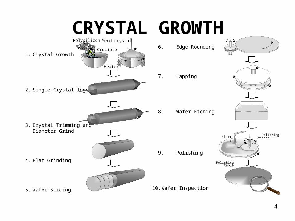
1. Crystal Growth
2. Single Crystal Ingot
3. Crystal Trimming and Diameter Grind
4. Flat Grinding
5. Wafer Slicing
6. Edge Rounding
7. Lapping
8. Wafer Etching
9. Polishing
10. Wafer Inspection
Slurry
Polishing table
Polishing head
Polysilicon Seed crystal
Heater
Crucible
CRYSTAL GROWTH
4
Starting Material Preparation
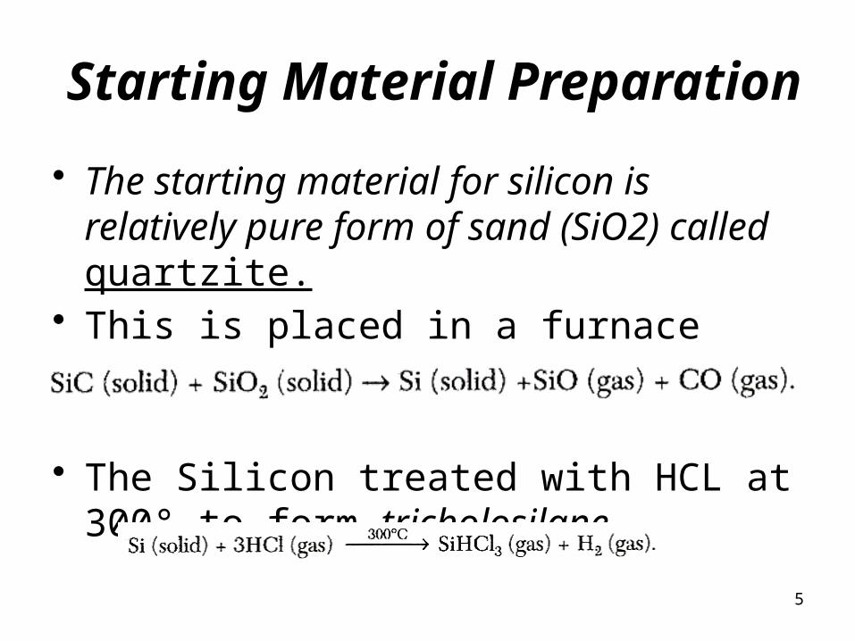
• The starting material for silicon is relatively pure form of sand (SiO2) called quartzite.
• This is placed in a furnace with various forms of Carbon.
• The Silicon treated with HCL at 300° to form tricholosilane.
5
Starting Material Preparation
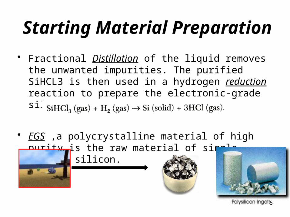
• Fractional Distillation of the liquid removes the unwanted impurities. The purified SiHCL3 is then used in a hydrogen reduction reaction to prepare the electronic-grade silicon ( EGS) .
• EGS ,a polycrystalline material of high purity is the raw material of single-crystal silicon.
6
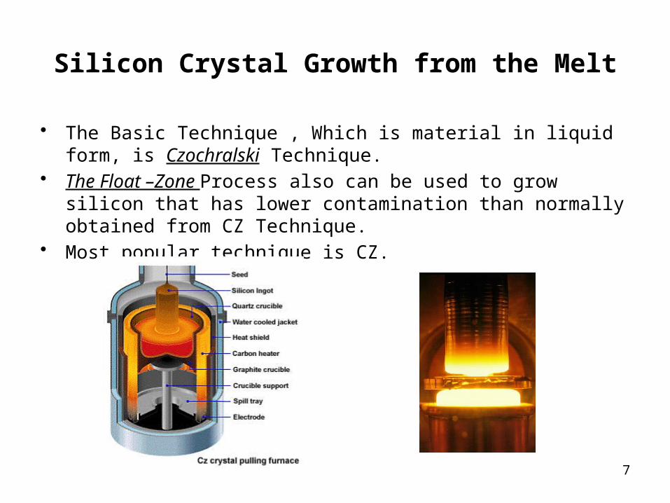
Silicon Crystal Growth from the Melt
• The Basic Technique , Which is material in liquid form, is Czochralski Technique.
• The Float –Zone Process also can be used to grow silicon that has lower contamination than normally obtained from CZ Technique.
• Most popular technique is CZ.
7
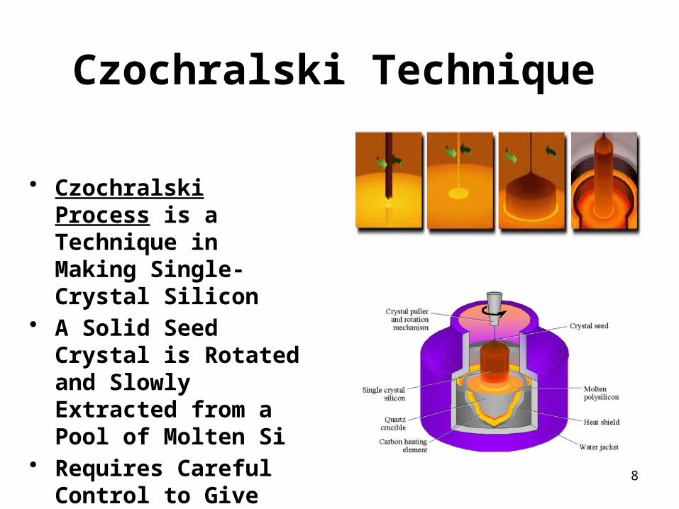
Czochralski Technique
• Czochralski Process is a Technique in Making Single-Crystal Silicon
• A Solid Seed Crystal is Rotated and Slowly Extracted from a Pool of Molten Si
• Requires Careful Control to Give Crystals Desired Purity and Dimensions 8
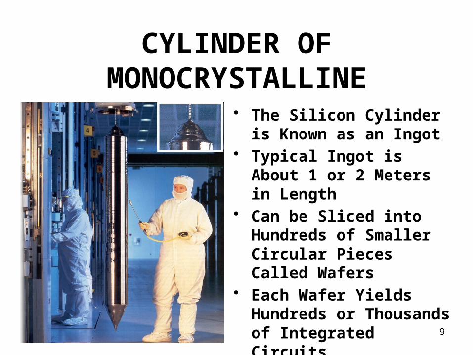
CYLINDER OF MONOCRYSTALLINE
• The Silicon Cylinder is Known as an Ingot
• Typical Ingot is About 1 or 2 Meters in Length
• Can be Sliced into Hundreds of Smaller Circular Pieces Called Wafers
• Each Wafer Yields Hundreds or Thousands of Integrated Circuits
9
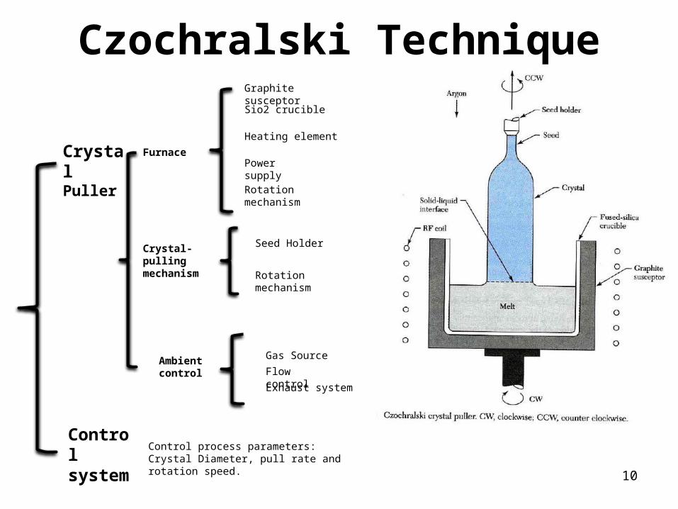
Czochralski Technique
Crystal Puller
Control system
Furnace
Graphite susceptor
Rotation mechanism
Heating element
Power supply
Crystal-pulling mechanism
Ambient control
Seed Holder
Sio2 crucible
Gas Source
Flow control
Rotation mechanism
Exhaust system
Control process parameters: Crystal Diameter, pull rate and rotation speed.
10
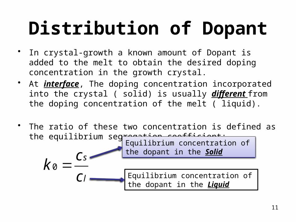
Distribution of Dopant• In crystal-growth a known amount of Dopant is added to the melt to
obtain the desired doping concentration in the growth crystal.• At interface, The doping concentration incorporated into the crystal
( solid) is usually different from the doping concentration of the melt ( liquid).
• The ratio of these two concentration is defined as the equilibrium segregation coefficient:
l
s
c
ck 0
Equilibrium concentration of the dopant in the Solid
Equilibrium concentration of the dopant in the Liquid
11
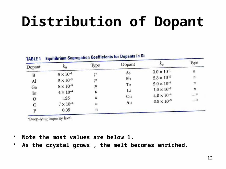
Distribution of Dopant
• Note the most values are below 1.• As the crystal grows , the melt becomes enriched.
12
Distribution of Dopant
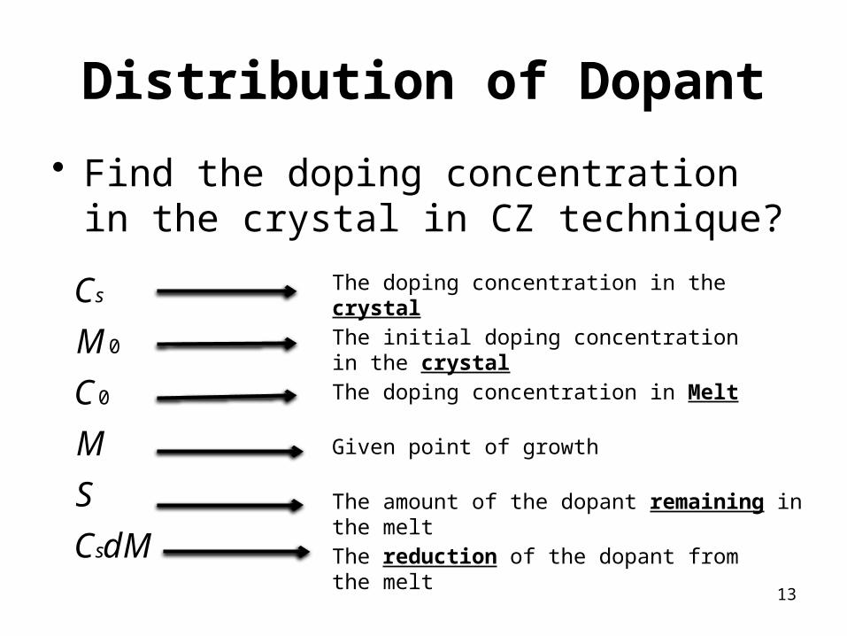
• Find the doping concentration in the crystal in CZ technique?
dMC
S
M
C
M
C
s
s
0
0
The doping concentration in the crystal
The initial doping concentration in the crystal
The doping concentration in Melt
Given point of growth
The amount of the dopant remaining in the melt
The reduction of the dopant from the melt
13
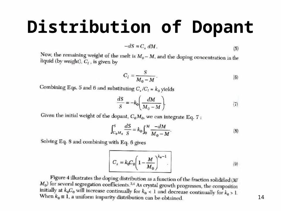
Distribution of Dopant
14
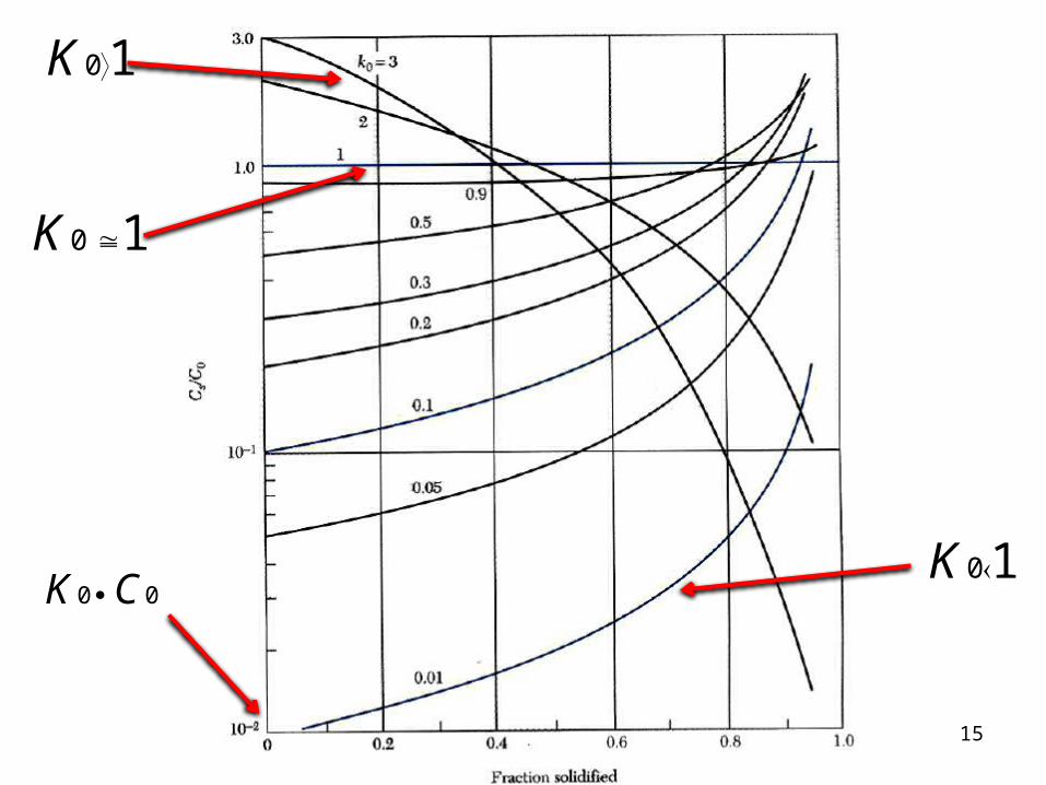
00 CK 10K
10K
10 K
15
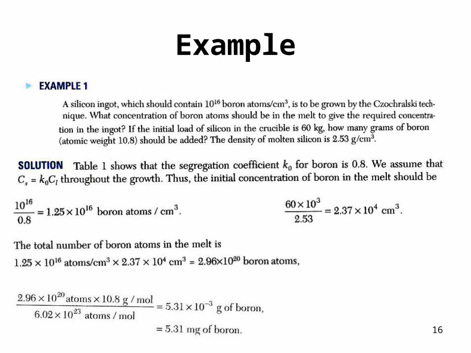
Example
16
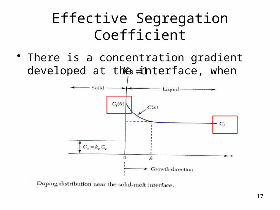
Effective Segregation Coefficient
• There is a concentration gradient developed at the interface, when . 10 K
17
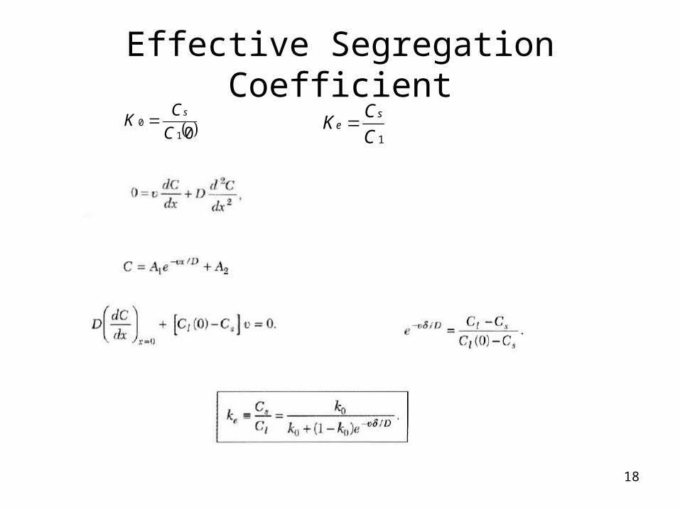
Effective Segregation Coefficient
1C
CK
se 01
0C
CK
s
18
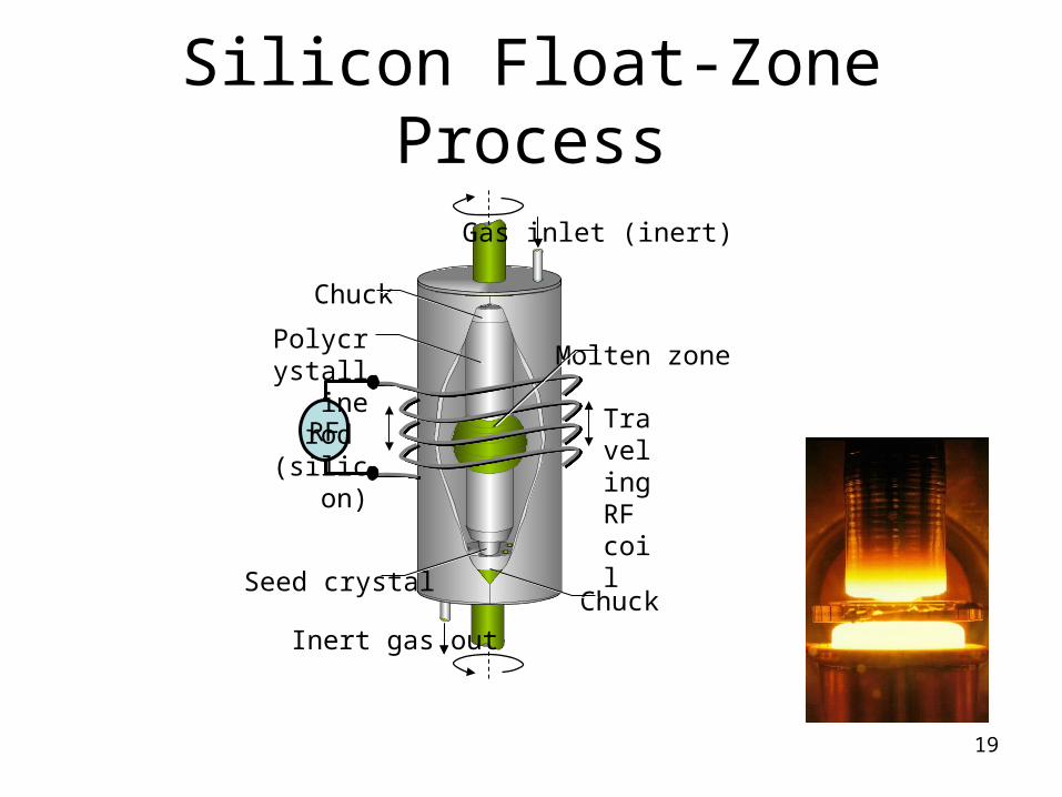
Silicon Float-Zone Process
RF
Gas inlet (inert)
Molten zone
Traveling RF coil
Polycrystalline rod (silicon)
Seed crystal
Inert gas out
Chuck
Chuck
19
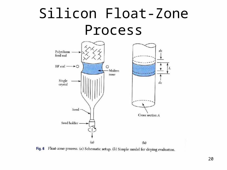
Silicon Float-Zone Process
20
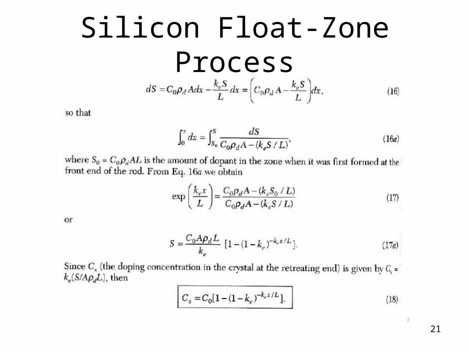
Silicon Float-Zone Process
21
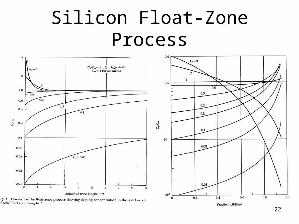
Silicon Float-Zone Process
22
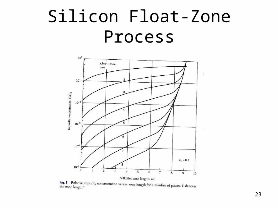
Silicon Float-Zone Process
23
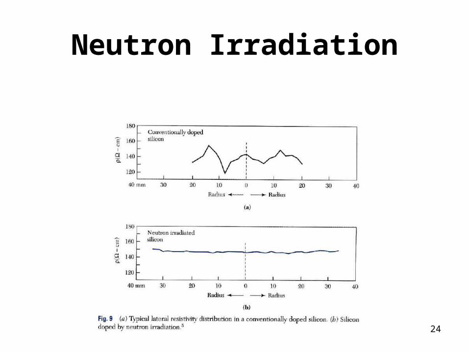
Neutron Irradiation
24
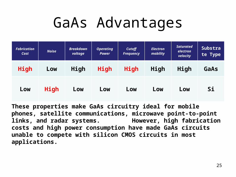
GaAs Advantages
Fabrication Cost Noise Breakdown
voltageOperating
PowerCutoff
FrequencyElectron mobility
Saturated electron velocity
Substrate Type
High Low High High High High High GaAs
Low High Low Low Low Low Low Si
25
These properties make GaAs circuitry ideal for mobile phones, satellite communications, microwave point-to-point links, and radar systems. However, high fabrication costs and high power consumption have made GaAs circuits unable to compete with silicon CMOS circuits in most applications.
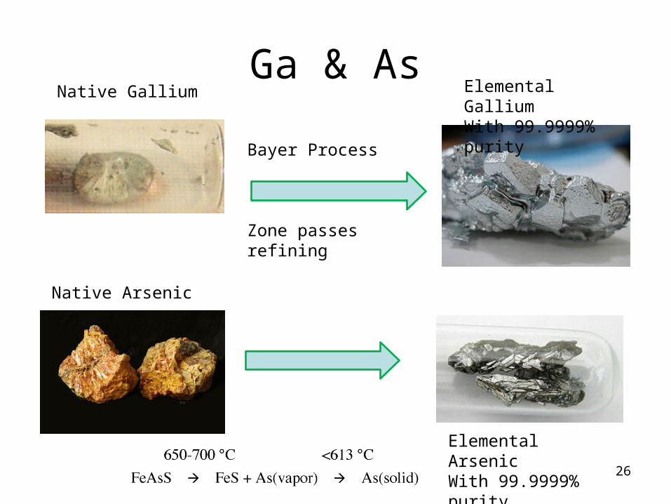
Ga & As
26
Native Gallium
Native Arsenic
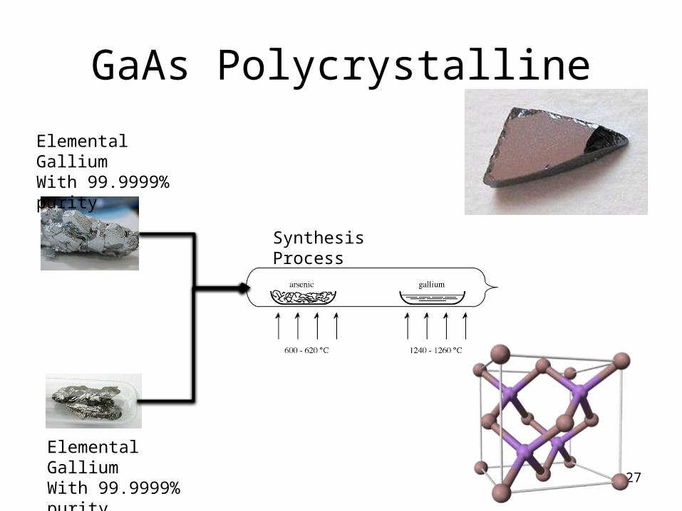
Elemental GalliumWith 99.9999% purity
Elemental ArsenicWith 99.9999% purity
Bayer Process
Zone passes refining
GaAs Polycrystalline
27
Elemental GalliumWith 99.9999% purity
Elemental GalliumWith 99.9999% purity
Synthesis Process
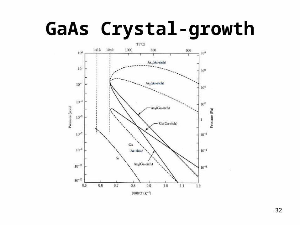
GaAs Crystal-growth
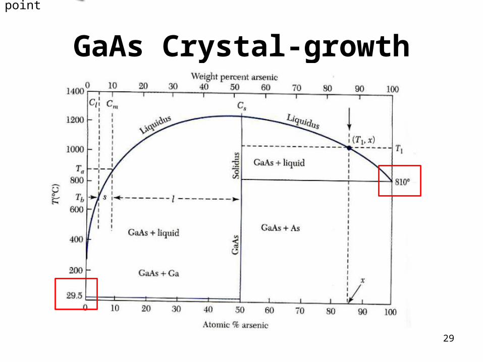
• The starting materials for the synthesis of polycrystalline gallium arsenide are the elemental , chemically pure gallium and arsenic.
• The behavior of a combination can be described by phase diagram.
28
GaAs Crystal-growth
29
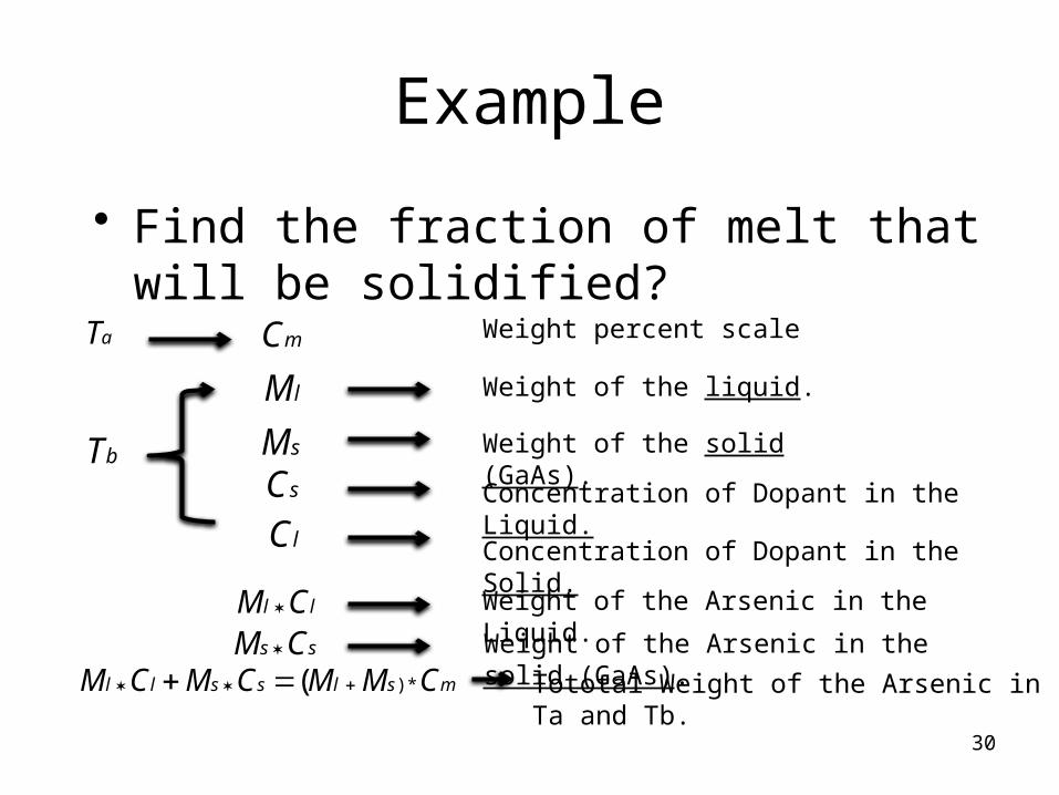
• Find the fraction of melt that will be solidified?
Example
30
aT
bT
mC
mslssll CMMCMCM *)( ss CM
ll CM
sClC
sM
lM
Weight percent scale
Weight of the liquid.
Weight of the solid (GaAs).
Concentration of Dopant in the Solid.
Concentration of Dopant in the Liquid.
Weight of the Arsenic in the Liquid.
Weight of the Arsenic in the solid (GaAs).
Tototal Weight of the Arsenic in Ta and Tb.
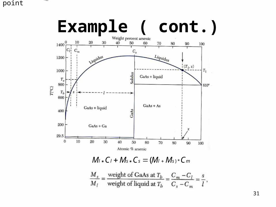
Example ( cont.)
31
mslssll CMMCMCM *)(
GaAs Crystal-growth
32
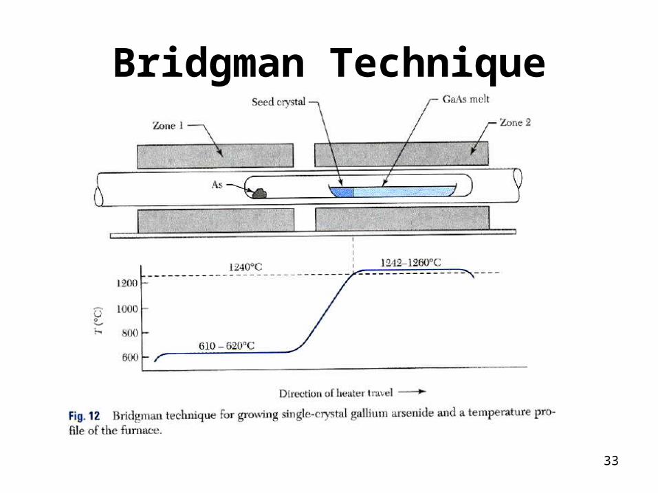
Bridgman Technique
33
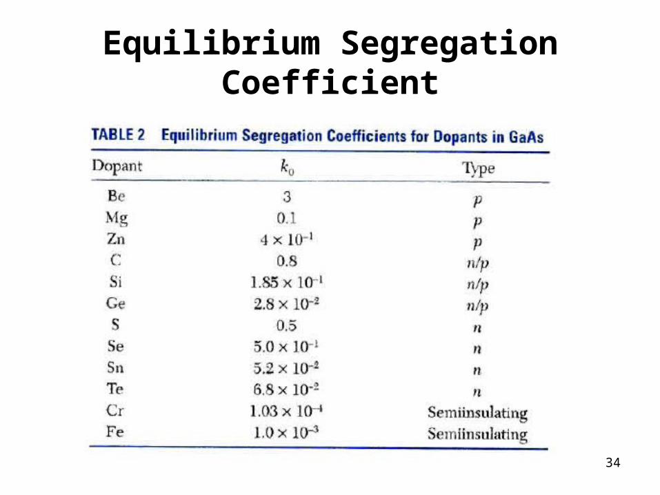
Equilibrium Segregation Coefficient
34
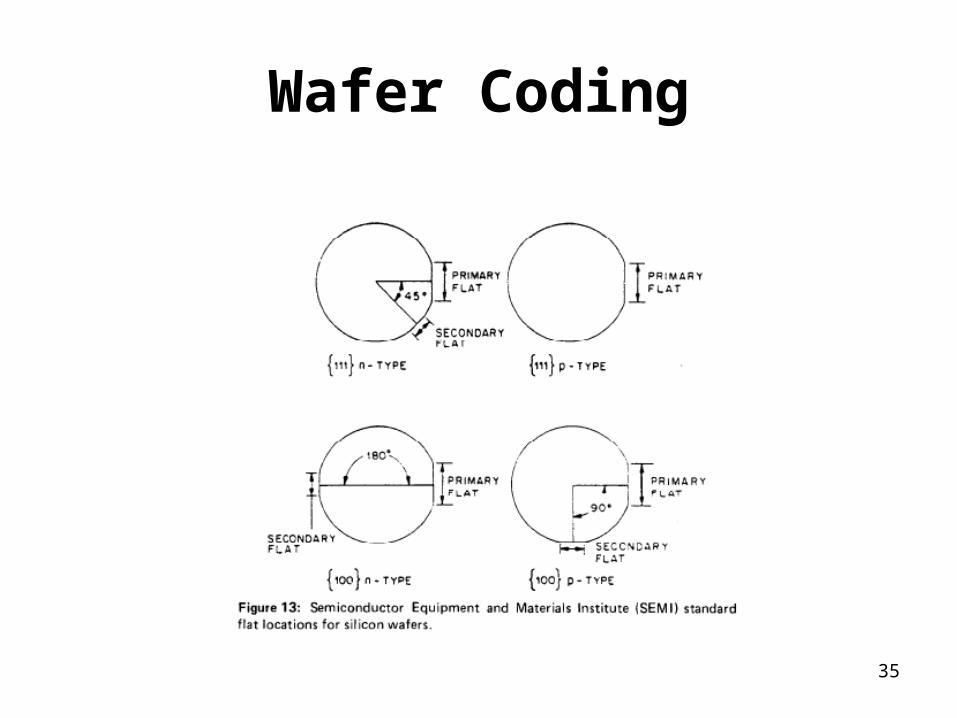
Wafer Coding
35
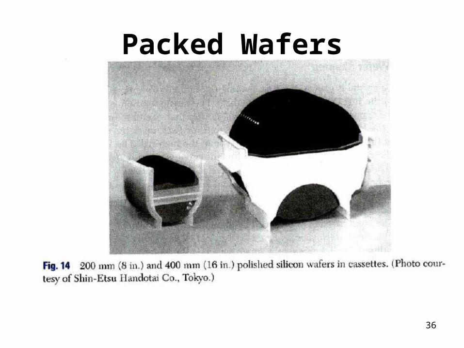
Packed Wafers
36
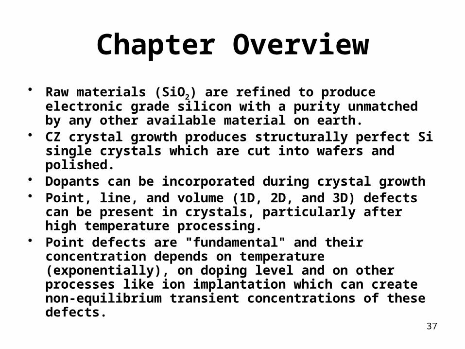
Chapter Overview• Raw materials (SiO2) are refined to produce electronic grade
silicon with a purity unmatched by any other available material on earth.
• CZ crystal growth produces structurally perfect Si single crystals which are cut into wafers and polished.
• Dopants can be incorporated during crystal growth • Point, line, and volume (1D, 2D, and 3D) defects can be present
in crystals, particularly after high temperature processing.• Point defects are "fundamental" and their concentration
depends on temperature (exponentially), on doping level and on other processes like ion implantation which can create non-equilibrium transient concentrations of these defects.
37