Chapter 1 · CHAPTER 1 INTRODUCTION 1.1 Mainboard Features CPU lSocket 7 supports Intel ® Pentium...
97
Transcript of Chapter 1 · CHAPTER 1 INTRODUCTION 1.1 Mainboard Features CPU lSocket 7 supports Intel ® Pentium...

CHAPTER 1 INTRODUCTION
Chapter 1
INTRODUCTION
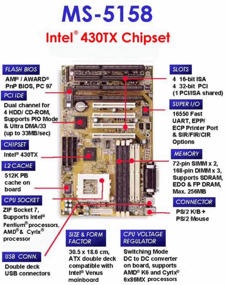
The MS-5158 is a high-performance personal computer mainboard. Thismainboard supports Intel® Pentium® /Pentium® with MMXTM technologyprocessors, Cyrix® 6x86/6x86L/6x86MX processors and AMD® K5/K6processors. The mainboard also supports four 32-bit PCI (PeripheralComponent Interconnect) Local Bus standard slots.
The mainboard uses the highly integrated Intel® 83430TX chipset to supportthe PCI/ISA and Green standards, and to provide the Host/PCI bridge. TheIntel® 82430TX chipset integrates all system control functions such as ACPI(Advanced Configuration and Power Interface). The ACPI provides moreEnergy Saving Features for the OSPM(OS Direct Power Management)function. The Intel® 82430TX chipset also improves the IDE transfer rate bysupporting Ultra DMA/33 IDE that transfer data at the rate of 33MB/s.
The mainboard also supports the LM78 Hardware Monitor Controller whichare optional functions. The LM78 function includes: CPU chassis/power fancontrol, CPU temperature detect and system voltage detect.
1-1
CHAPTER 1 INTRODUCTION
1.1 Mainboard Features
CPUl Socket 7 supports Intel® Pentium® and Pentium® with MMX™
technology processorsl The Cyrix® 6x86/6x86L/6x86MX and AMD® K5/K6 processors are also
supported.
Chipsetl Intel® 82430TX chipset.
Cache Memoryl Supports 512K pipelined burst cache memory.l Supports Direct Map Organization and Write-Back cache policy.
Main Memoryl Supports five memory banks using two 72-pin SIMM sockets and three
168-pin DIMM sockets (for unbuffered DIMM).l Up to 256 Mbytes main memory.l Supports EDO Hyper Page Mode DRAM, Standard Fast Page mode
DRAM and SDRAM(Synchronous DRAM).
Slotsl Four 32-bit PCI Bus slots (four 32-bit bus master PCI slots + four 16-bit
ISA bus slots). One shared slot can be used as ISA or PCI.
On-Board IDEl Supports Bus Master and Ultra DMA/33 IDE.l Supports up to 4 IDE drives.
On-Board Peripheralsl On-Board Peripherals include:
- 1 floppy port supports 2 FDD- 2 serial ports (COMA + COMB)- 1 parallel port supports ECP or EPP mode- USB Ports- IR (reserved)
1-2
CHAPTER 1 INTRODUCTION
1-3
Dimensionsl Standard ATX form factorl 30cm(L) x 18.6cm(W) x 4 layer PCBl Double deck I/O connectors, compatibles with Intel® Venus mainboard
Mountingl 6 mounting holes
LM78 System Hardware Monitor(optional)l CPU fan Rotation Speed Controll CPU Fan Control/Power Fan Control (the fan will automatically stop when
the system enters suspend mode)l System Voltage Detectl CPU Overheat Warning (reserved)l Chassis Intrusion Detect(reserved)l Display Actual Current Voltage
Other Featuresl Poly Fuse used by keyboard and USB devicesl Keyboard password wake up system(reserved)l CPU Vcore voltage protectl Meets ACPI specificationsl Power ON/OFF switch connector on boardl Soft Power-Offl Ring Wake-Upl Alarm Wake-Up

CHAPTER 1 INTRODUCTION
1.2 Parts of the Mainboard
1-4
A
B
C
D
EG
H
J
K
L
NOP
F
I
M
CHAPTER 1 INTRODUCTION
1-5
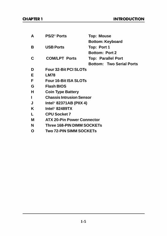
A PS/2® Ports Top: MouseBottom: Keyboard
B USB Ports T op: Port 1Bottom: Port 2
C COM/LPT Ports Top: Parallel PortBottom: Two Serial Ports
D Four 32-Bit PCI SLOTsE LM78F Four 16-Bit ISA SLOTsG Flash BIOSH Coin Type BatteryI Chassis Intrusion SensorJ Intel ® 82371AB (PIIX 4)K Intel ® 82489TXL CPU Socket 7M ATX 20-Pin Power ConnectorN Three 168-PIN DIMM SOCKETsO Two 72-PIN SIMM SOCKETs
CHAPTER 1 INTRODUCTION
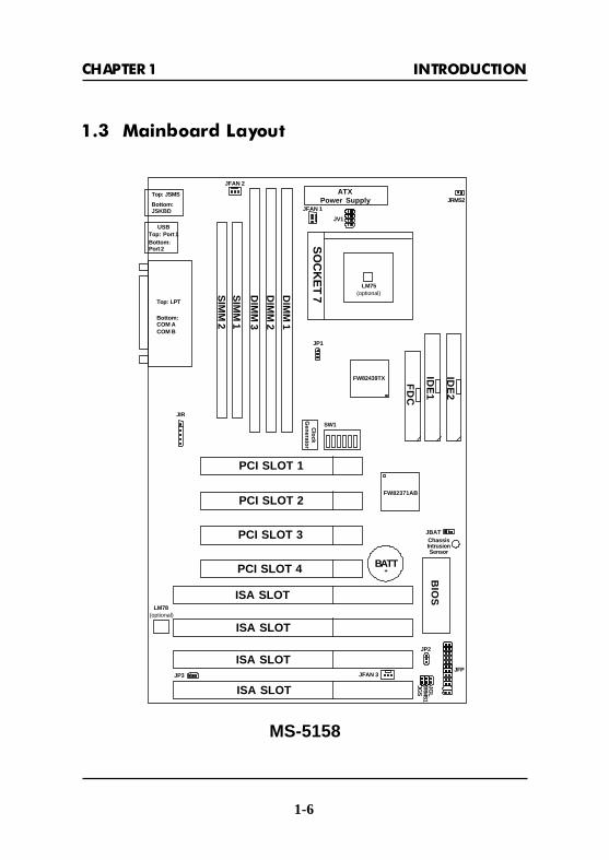
1.3 Mainboard Layout
1-6
MS-5158
ISA SLOT
ISA SLOT
ISA SLOT
PCI SLOT 4
PCI SLOT 3
PCI SLOT 2
PCI SLOT 1
DIM
M 1
SO
CK
ET
7
ISA SLOT
DIM
M 2
DIM
M 3
SIM
M 1
FD
C
BATT+
SIM
M 2
IDE
1B
IOS
ATXPower Supply
FW82371AB
FW82439TX
JGL
JFP
IDE
2
JGS
JIR
JP2
JP1
JV1
JBAT
SW1
JFAN 2
JFAN 1
JRM
S1
Top: JSMS
Bottom:JSKBD
Top: Port 1USB
Bottom:Port 2
Top: LPT
Bottom:COM ACOM B
LM75(optional)
LM78(optional)
JP3 JFAN 3
Clock
Generator
ChassisIntrusionSensor
JRMS2

CHAPTER 2 HARDWARE INSTALLATION
Chapter 2
HARDWARE INSTALLATION
2.1 Central Processing Unit: CPU
The MS-5158 system board operates with Intel ® Pentium®/Pentium® withMMX ™ technology, Cyrix ® 6x86/6x86L/6x86MX and AMD ® K5/K6processors. It could operate with 2.1V to 3.5V processors. The mainboardprovides a 321-pin ZIF Socket 7 for easy CPU installation, a DIP switch(SW1) to set the proper speed for the CPU and a Jumper block (JV1) forsetting the CPU voltage. The CPU should always have a cooling fanattached to prevent overheating.
CPU
CPU
2.1-1 CPU Installation Procedures
2-1
3. Press the lever down tocomplete the installation.
2. Locate Pin 1 in the socketand look for the white dot orcut edge in the CPU. MatchPin 1 with the white dot/cutedge. Then, insert the CPU.It should insert easily.
Open Lever
Pin 1
SlidingPlate
White dot/Cut edge
CloseLever
1. Pull the lever sideways awayfrom the socket. Then raisethe lever up to a 90-degreeangle.
CHAPTER 2 HARDWARE INSTALLATION
4 5 6 Clock
OFF OFF ON 50MHz
ON ON OFF 55MHz
ON OFF OFF 60MHz
OFF OFF OFF 66.8MHz
OFF ON OFF 75MHz
ON ON ON 83MHz
4 5 6 Clock
ON ON ON 50MHz
ON OFF OFF 60MHz
OFF OFF OFF 66.6MHz
OFF ON OFF 75MHz
ON OFF ON 83MHz
SW1 CPU
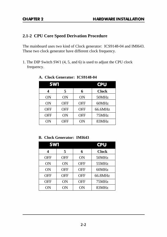
2.1-2 CPU Core Speed Derivation Procedure
The mainboard uses two kind of Clock generator: ICS9148-04 and IMI643.These two clock generator have different clock frequency.
1. The DIP Switch SW1 (4, 5, and 6) is used to adjust the CPU clockfrequency.
A. Clock Generator: ICS9148-04
SW1 CPU
B. Clock Generator: IMI643
2-2

CHAPTER 2 HARDWARE INSTALLATION
1 2 3 Core/Bus Ratio
OFF OFF OFF 1.5 /3.5
ON OFF OFF 2
ON ON OFF 2.5
OFF ON OFF 3
ON OFF ON 4
ON ON ON 4.5
2. The DIP Switch SW1 (1, 2, and 3) is used to set the Core/Bus(Fraction) ratio of the CPU. The actual core speed of the CPU is theHost Clock Frequency multiplied by the Core/Bus ratio. For example:
If CPU Clock = 66MHzCore/Bus ratio = 3/2
then CPU core speed = Host Clock x Core/Bus ratio
= 66MHz x 3/2= 100MHz
3. The PCI Bus Clock is the CPU Clock Frequency divided by 2.
SW1 CPU
2-3

CHAPTER 2 HARDWARE INSTALLATION
2-4
2.1-3 CPU Voltage Setting: JV1
JV1
VcoreV I/O
3.5 3.5
3.3 3.3
3.3 3.2
3.3 2.9
JV1
1
2
3
4
1
2
3
4
1
2
3
4
1
2
3
4
1
2
3
4
CHAPTER 2 HARDWARE INSTALLATION
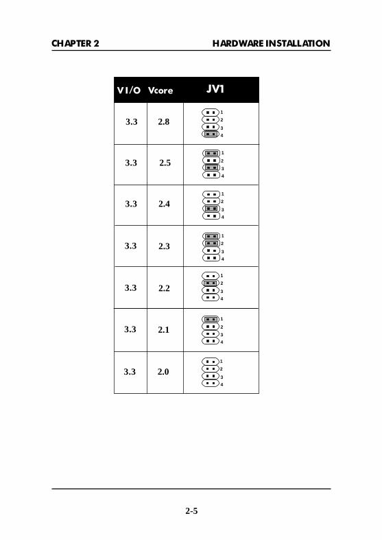
VcoreV I/O
3.3 2.8
3.3 2.5
3.3 2.4
3.3 2.3
3.3 2.2
JV1
1
2
3
4
1
2
3
4
1
2
3
4
1
2
3
4
3.3 2.11
2
3
4
2-5
1
2
3
4
3.3 2.01
2
3
4
CHAPTER 2 HARDWARE INSTALLATION
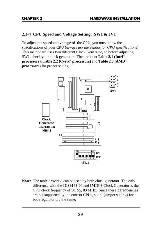
To adjust the speed and voltage of the CPU, you must know thespecifications of your CPU (always ask the vendor for CPU specifications).This mainboard uses two different Clock Generator, so before adjustingSW1, check your clock generator. Then refer to Table 2.1 (Intel®
processors), Table 2.2 (Cyrix® processors) and Table 2.3 (AMD®
processors) for proper setting.
2.1-4 CPU Speed and Voltage Setting: SW1 & JV1
2-6
SW1
1 2 3 4 5 6
ON DIPON
OFF
1
2
3
4
JV1
ClockGenerator
ICS9148-04/IMI643
Note: The table provided can be used by both clock generator. The onlydifference with the ICS9148-04 and IMI643 Clock Generator is theCPU clock frequency of 50, 55, 83 MHz. Since these 3 frequenciesare not supported by the current CPUs, so the jumper settings forboth regulator are the same.
CHAPTER 2 HARDWARE INSTALLATION
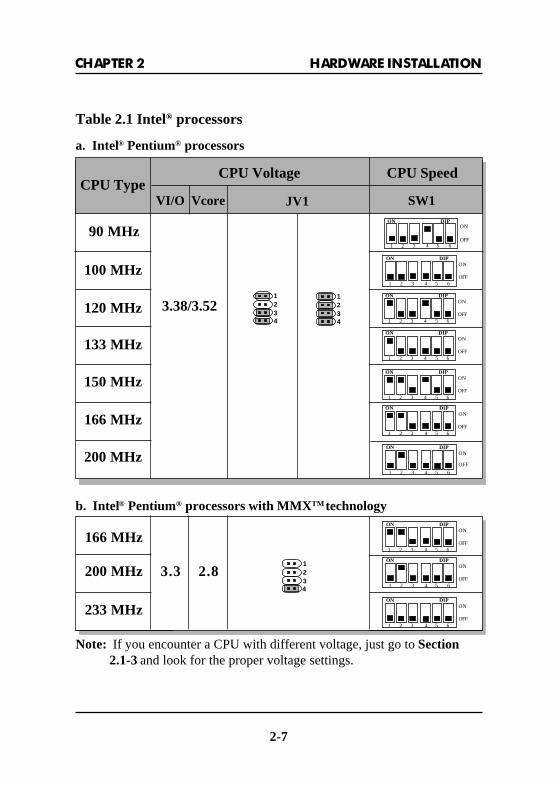
Table 2.1 Intel® processors
90 MHz
100 MHz
120 MHz
133 MHz
150 MHz
166 MHz
200 MHz
3.38/3.52
CPU TypeCPU SpeedCPU Voltage
SW1VI/O Vcore
2-7
JV1
ON DIP
1 2 3 4 5 6
ON
OFF
ON DIP
1 2 3 4 5 6
ON
OFF
ON DIP
1 2 3 4 5 6
ON
OFF
166 MHz
200 MHz 3.3 2.8
233 MHz
b. Intel® Pentium® processors with MMXTM technology
a. Intel® Pentium® processors
1234
1234
1234
Note: If you encounter a CPU with different voltage, just go to Section2.1-3 and look for the proper voltage settings.
ON DIP
1 2 3 4 5 6
ON
OFF
ON DIP
1 2 3 4 5 6
ON
OFF
ON DIP
1 2 3 4 5 6
ON
OFF
ON DIP
1 2 3 4 5 6
ON
OFF
ON DIP
1 2 3 4 5 6
ON
OFF
ON DIP
1 2 3 4 5 6
ON
OFF
ON DIP
1 2 3 4 5 6
ON
OFF

CHAPTER 2 HARDWARE INSTALLATION
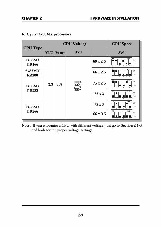
Table 2.2 Cyrix® 6x86/6x86L/6x86MX processors
Cyrix® CPU uses PR to rate the speed of their processors based on Intel®
processor core speed. For example PR150 (120MHz) has 150MHz corespeed of Intel® processors but has 120MHz core speed in Cyrix®. Cyrix®
CPU should always uses a more powerful fan (ask vendor for propercooling fan).
3.5
CPU TypeCPU SpeedCPU Voltage
SW1VI/O Vcore
6x86PR150
6x86PR166
6x86PR200
2-8
3.3 2.8
JV1
6x86LPR166
3.5
1234
1234
1234
6x86LPR200
ON DIP
1 2 3 4 5 6
ON
OFF
ON DIP
1 2 3 4 5 6
ON
OFF
ON DIP
1 2 3 4 5 6
ON
OFF
3.3 2.8
1234
a. Cyrix® 6x86/6x86L processors
CHAPTER 2 HARDWARE INSTALLATION
CPU TypeCPU SpeedCPU Voltage
SW1VI/O Vcore
6x86MXPR166
6x86MXPR233
3.3 2.9
JV1
6x86MXPR200
6x86MXPR266
60 x 2.5
75 x 2.5
66 x 3
75 x 3
b. Cyrix® 6x86MX processors
Note: If you encounter a CPU with different voltage, just go to Section 2.1-3and look for the proper voltage settings.
2-9
ON DIP
1 2 3 4 5 6
ON
OFF
ON DIP
1 2 3 4 5 6
ON
OFF
ON DIP
1 2 3 4 5 6
ON
OFF
ON DIP
1 2 3 4 5 6
ON
OFF
ON DIP
1 2 3 4 5 6
ON
OFF
ON DIP
1 2 3 4 5 6
ON
OFF66 x 3.5
66 x 2.5
1234

CHAPTER 2 HARDWARE INSTALLATION
Table 2.3 AMD® processorsAMD® K5/K6 CPU uses PR to rate the speed of their processors based onIntel® processor core speed . For example PR133(100MHz) has 133MHzcore speed of Intel® processors but has 100MHz core speed in AMD® K5processor.
ON DIP
1 2 3 4 5 6
ON
OFF
3.52
ON DIP
1 2 3 4 5 6
ON
OFF
1 2 3 4 5 6
CPU TypeCPU SpeedCPU Voltage
SW1VI/O Vcore
PR100
PR120ON DIP
1 2 3 4 5 6
ON
OFF
2-10
PR133/PR150
JV1
PR90
PR166
ON DIPON
OFF
ON DIPON
OFF
ON DIP
1 2 3 4 5 6
ON
OFF
3.3ON DIP
1 2 3 4 5 6
ON
OFFPR200
PR233ON DIP
1 2 3 4 5 6
ON
OFF
PR1662.9
b. AMD® K6 processors
3.3 3.2
Note: If you encounter a CPU with different voltage, just go to Section2.1-3 and look for the proper voltage settings.
a. AMD® K5 processors
1234
1234
1234

CHAPTER 2 HARDWARE INSTALLATION
2.1-5 CPU Fan Power Connector: JFAN1 / JFAN2 &JFAN3 (Reserved)
These connectors support system cooling fan with +12V. It supports threepin head connector. When connecting the wire to the connector, alwaystake note that the red wire is the positive and should be connected to the+12V, the black wire is Ground and should be connected to GND. If yourmainboard has LM78 on board, you need to use a specially designed fanwith speed sensor to take advantage of LM78’s CPU fan control function.
Note: 1. JFAN2 & JFAN3 are the Power and Chassis Cooling Fan SpeedConnectors (reserved for LM78 System Hardware Monitor Option.)2. Always consult vendor for proper CPU cooling fan.
2-11
JFAN2
SPEED
+12V
GND
JFAN1
+12V
SPEED
GND
JFAN3
SPEED
+12V
GND
JFAN1: CPU FANJFAN2: POWER FANJFAN3: CHASSIS FAN
For fans with fan speed sensor, every rotation of the fan will send out 2pulses. LM78 will count and report the fan rotation speed.
CHAPTER 2 HARDWARE INSTALLATION
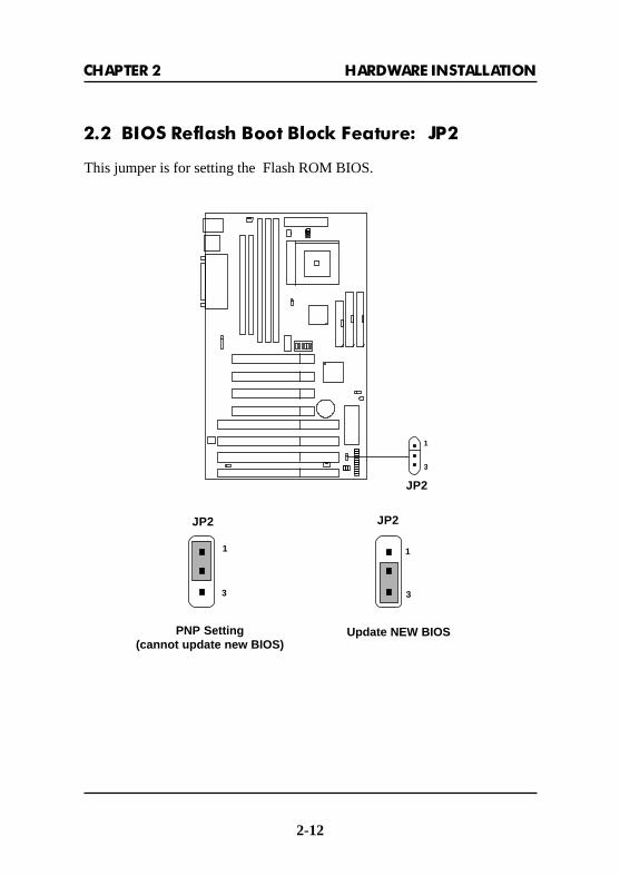
2.2 BIOS Reflash Boot Block Feature: JP2
This jumper is for setting the Flash ROM BIOS.
JP2
1
3
JP2 JP2
Update NEW BIOSPNP Setting(cannot update new BIOS)
1 1
33
2-12

CHAPTER 2 HARDWARE INSTALLATION
2.3 Internal Modem Ring Wake-up Connector: JP3
The JP3 connector is used for special internal modem that has 3 pins thatsupport the ring power on function. The 3 pins of the internal modemshould have the same pin definition with JP3.
JP31 3
Pin 1: Standby 5V
Pin 2: Ring Single Input
Pin 3: Ground
2-13
CHAPTER 2 HARDWARE INSTALLATION
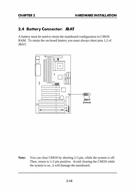
2.4 Battery Connector: JBAT
A battery must be used to retain the mainboard configuration in CMOSRAM. To retain the on-board battery you must always short pins 1,2 ofJBAT.
2-14
Note: You can clear CMOS by shorting 2-3 pin, while the system is off.Then, return to 1-2 pin position. Avoid clearing the CMOS whilethe system is on , it will damage the mainboard.
JBAT(Default)
1 3
CHAPTER 2 HARDWARE INSTALLATION
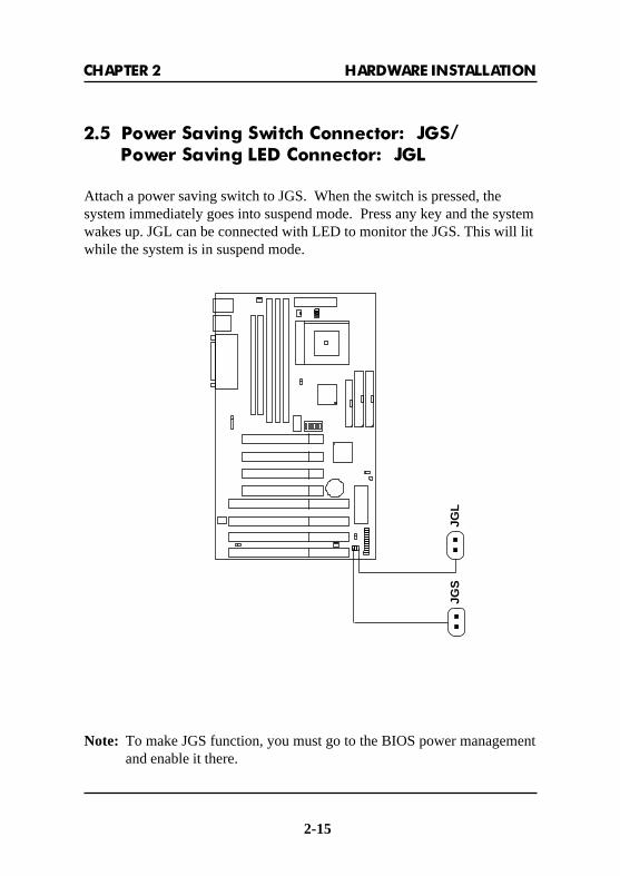
2.5 Power Saving Switch Connector: JGS/ Power Saving LED Connector: JGL
Attach a power saving switch to JGS. When the switch is pressed, thesystem immediately goes into suspend mode. Press any key and the systemwakes up. JGL can be connected with LED to monitor the JGS. This will litwhile the system is in suspend mode.
JGS
2-15
Note: To make JGS function, you must go to the BIOS power managementand enable it there.
JGL
CHAPTER 2 HARDWARE INSTALLATION
2-16
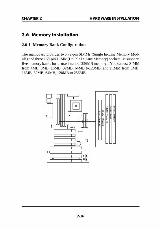
2.6 Memory Installation
2.6-1 Memory Bank Configuration
The mainboard provides two 72-pin SIMMs (Single In-Line Memory Mod-ule) and three 168-pin DIMM(Double In-Line Memory) sockets. It supportsfive memory banks for a maximum of 256MB memory. You can use SIMMfrom 4MB, 8MB, 16MB, 32MB, 64MB to128MB, and DIMM from 8MB,16MB, 32MB, 64MB, 128MB to 256MB.
SIM
M1(B
ank 3)
SIM
M2(B
ank3)
DIM
M2(B
ank 1)
DIM
M3 (B
ank 2)
DIM
M1(B
ank 0)

CHAPTER 2 HARDWARE INSTALLATION
2.6-2 Memory Installation Procedures:
1. The SIMM slot has a “Plastic SafetyTab” and the SIMM memory modulehas a “Notched End”, so the SIMMmemory module can only fit in onedirection.
2. Insert the SIMM memory modules intothe socket at 45-degree angle. Then,push into a vertical position so that itwill snap into place.
3. The Mounting Holes and Metal Clipsshould fit over the edge and hold theSIMM memory modules in place.
A. How to install SIMM Module
Single Sided SIMM
Double Sided SIMM
Notched End
2-17

CHAPTER 2 HARDWARE INSTALLATION
B. How to install DIMM Module
1. The DIMM slot has two keys marked “VOLT and DRAM” , so theDIMM memory module can only fit in one direction.
2. Insert the DIMM memory module vertically into the DIMM slot.Then, push it in.
3. Close the plastic clip at the side of the DIMM slot.
Single Sided DIMM
Double Sided DIMM
2-18
DRAM VOLT
CHAPTER 2 HARDWARE INSTALLATION
2-19
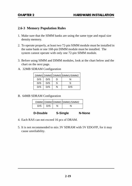
1. Make sure that the SIMM banks are using the same type and equal sizedensity memory.
2. To operate properly, at least two 72-pin SIMM module must be installed inthe same bank or one 168-pin DIMM module must be installed. Thesystem cannot operate with only one 72-pin SIMM module.
3. Before using SIMM and DIMM modules, look at the chart below and thechart on the next page.
2.6-3 Memory Population Rules
A. 32MB SDRAM Configuration
DIMM1 DIMM2 DIMM3 SIMM1/SIMM2
D/S D/S D N
D/S D/S S S
D/S D/S N D/S
B. 64MB SDRAM Configuration
DIMM1 DIMM2 DIMM3 SIMM1/SIMM2
D/S D/S N N
D-Double S-Single N-None
4. Each RAS can not exceed 16 pcs of DRAM.
5. It is not recommended to mix 3V SDRAM with 5V EDO/FP, for it maycause unreliability.
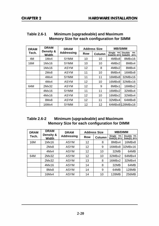
CHAPTER 2 HARDWARE INSTALLATION
4M 1Mx4 SYMM 10 10 4MBx8 8MBx16
16M 1Mx16 SYMM 10 10 4MBx2 8MBx4
1Mx16 ASYM 12 8 4MBx2 8MBx4
2Mx8 ASYM 11 10 8MBx4 16MBx8
4Mx4 SYMM 11 11 16MBx8 32MBx16
4Mx4 ASYM 12 10 16MBx8 32MBx16
64M 2Mx32 ASYM 12 9 8MBx1 16MBx2
4Mx16 SYMM 11 11 16MBx2 32MBx4
4Mx16 ASYM 12 10 16MBx2 32MBx4
8Mx8 ASYM 12 11 32MBx4 64MBx8
16Mx4 SYMM 12 12 64MBx8 128MBx16
16M 1Mx16 ASYM 12 8 8MBx4 16MBx8
2Mx8 ASYM 12 9 16MBx8 32MBx16
4Mx4 ASYM 12 10 32MB 64MB
64M 2Mx32 ASYM 12 10 32MBx2 64MBx4
2Mx32 ASYM 13 8 16MBx2 32MBx4
4Mx16 ASYM 14 8 32MB 64MB
8Mx8 ASYM 14 9 64MB 128MB
16Mx4 ASYM 14 10 128MB 256MB
DRAMTech.
DRAMDensity &
Width
DRAMAddressing
Address Size MB/SIMM
Row Column SingleSide(S)
DoubleSide(D)
DRAMTech.
DRAMDensity &
Width
DRAMAddressing
Address Size MB/DIMM
Row Column SingleSide(S)
DoubleSide(D)
Table 2.6-1 Minimum (upgradeable) and Maximum Memory Size for each configuration for SIMM
Table 2.6-2 Minimum (upgradeable) and Maximum Memory Size for each configuration for DIMM
no.pcs.
no.pcs.
no.pcs.
no.pcs.
2-20

CHAPTER 2 HARDWARE INSTALLATION
2.7 Case Connector: JFP
The Turbo LED, Hardware Reset, Key Lock, Power LED, Power SavingLED, Sleep Switch, Speaker and HDD LED are all grouped in JFP connec-tor block for easy installation.
1xx
1122
21
SpeakerPower LED
Keylock
Turbo LEDReset Switch
HDD LED
10
20
+
++
+
PowerSavingLED
Figure 2.1
2-21
JFP
1
10
21

CHAPTER 2 HARDWARE INSTALLATION
2.7-1 Turbo LED
This mainboard is always on Turbo speed. Connecting a Turbo LED will justlit the LED. (See Figure 2.1)
2.7-2 Hardware Reset
Reset switch are used to reboot the system rather than turning the powerON/OFF. Avoid rebooting the system when the HDD LED is lit. You canconnect the Reset switch from the system case to this pin. (See Figure 2.1)
2.7-3 Keylock
Keylock allows you to disable the keyboard for security purposes. You canconnect the keylock to this pin. (See Figure 2.1)
2.7-4 Power LED
The Power LED is always lit while the system power is on. You can connectthe Power LED from the system case to this pin. (See Figure 2.1)
2.7-5 Speaker
Speaker from the system case are connected to this pin. (See Figure 2.1)
2.7-6 HDD LED
HDD LED shows the activity of a hard disk drive. Avoid turning thepower off while the HDD led is lit. You can connect the HDD LED fromthe system case to this pin. (See Figure 2.1).
2-22

CHAPTER 2 HARDWARE INSTALLATION
2.8 Floppy Disk Connector: FDC
The mainboard also provides a standard floppy disk connector, FDC thatsupports 360K, 720K, 1.2M, 1.44M and 2.88M floppy disk types. You canattach a floppy disk cable directly to this connector.
FDC
1
2-23

CHAPTER 2 HARDWARE INSTALLATION
2.9 Hard Disk Connectors: IDE1 & IDE2
The mainboard has a 32-bit Enhanced PCI IDE Controller that provides fortwo HDD connectors IDE1 (primary) and IDE2 (secondary). You canconnect up to four hard disk drives, CD-ROM, 120MB Floppy (reserved forfuture BIOS) and other devices to IDE1 and IDE2.
IDE1(primary IDE connector)
The first hard disk should always be connected to IDE1. IDE1 canconnect a Master and a Slave drive.
IDE2(secondary IDE connector)
IDE2 can connect a Master and a Slave drive.
2-24
Prim
ary
IDE
Con
nect
or
Sec
onda
ry I
DE
Con
nect
or
11

CHAPTER 2 HARDWARE INSTALLATION
2.10 ATX 20-pin Power Connector: JWR1
This type of connector already supports the remote ON/OFF function.However, you need to connect the Remote Power On/OFF switch(JRMS1 or JRMS2).
5V 5V -5V
5V5V
3.3V-12V
12V 5V_SB 3.3V3.3V
GND GND GNDGND
GNDGNDGNDPW_OK
PS_ON
12345678910
11121314151617181920
ATX Power Connector Pin Description
ATXPower Connector
2-25
101
11 20
CHAPTER 2 HARDWARE INSTALLATION
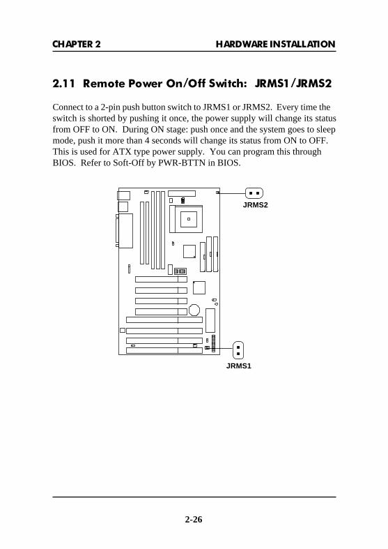
2.11 Remote Power On/Off Switch: JRMS1/JRMS2
Connect to a 2-pin push button switch to JRMS1 or JRMS2. Every time theswitch is shorted by pushing it once, the power supply will change its statusfrom OFF to ON. During ON stage: push once and the system goes to sleepmode, push it more than 4 seconds will change its status from ON to OFF.This is used for ATX type power supply. You can program this throughBIOS. Refer to Soft-Off by PWR-BTTN in BIOS.
JRMS2
2-26
JRMS1
CHAPTER 2 HARDWARE INSTALLATION
TX
GND
RX
NC
VCC
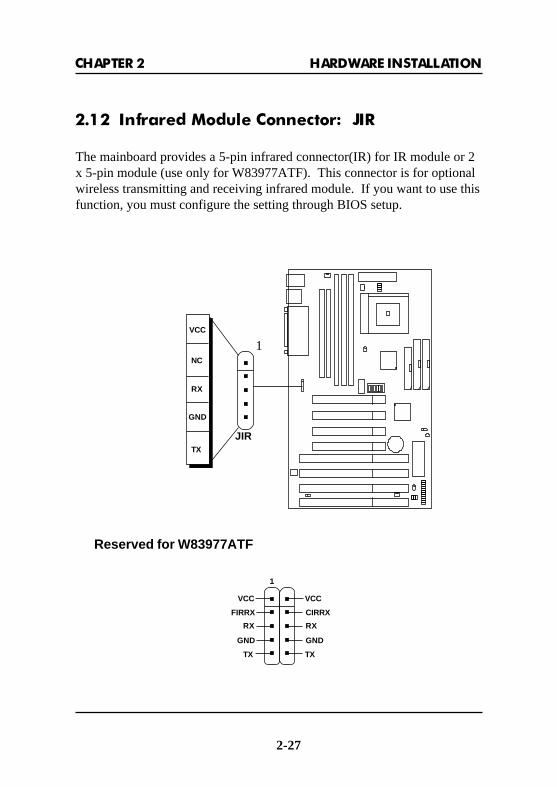
2.12 Infrared Module Connector: JIR
The mainboard provides a 5-pin infrared connector(IR) for IR module or 2x 5-pin module (use only for W83977ATF). This connector is for optionalwireless transmitting and receiving infrared module. If you want to use thisfunction, you must configure the setting through BIOS setup.
2-27
JIR
1
Reserved for W83977ATF
VCC
CIRRX
RX
GND
TX
VCC
FIRRX
RX
GND
TX
1

CHAPTER 2 HARDWARE INSTALLATION
2.13 Serial Port Connectors: COM A & COM B
The mainboard has two serial ports COMA and COMB. These two portsare 16550A high speed communication ports that send/receive 16 bytesFIFOs. You can attach a mouse or a modem cable directly into theseconnectors.
PIN DEFINITION
Pin # Definition
1 DCD(Data Carry Detect)
2 SIN(Serial In or Receive Data)
3 SOUT(Serial Out or Transmit Data)
4 DTR(Data Terminal Ready)
5 GND
6 DSR(Data Set Ready)
7 RTS(Request To Send)
8 CTS(Clear To Send)
9 RI(Ring Indicate)
1 2 3 4 5
6 7 8 9
COM A COM B
Serial Ports (9-pin Male)
2-28
CHAPTER 2 HARDWARE INSTALLATION
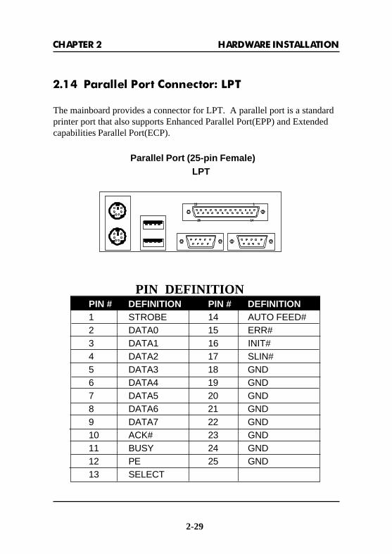
2.14 Parallel Port Connector: LPT
The mainboard provides a connector for LPT. A parallel port is a standardprinter port that also supports Enhanced Parallel Port(EPP) and Extendedcapabilities Parallel Port(ECP).
PIN # DEFINITION PIN # DEFINITION1 STROBE 14 AUTO FEED#2 DATA0 15 ERR#3 DATA1 16 INIT#4 DATA2 17 SLIN#5 DATA3 18 GND6 DATA4 19 GND7 DATA5 20 GND8 DATA6 21 GND9 DATA7 22 GND10 ACK# 23 GND11 BUSY 24 GND12 PE 25 GND13 SELECT
PIN DEFINITION
LPTParallel Port (25-pin Female)
1
25 14
13
2-29

CHAPTER 2 HARDWARE INSTALLATION
2.15 Keyboard Connector: PSKBC Mouse Connector: PSMSC
The mainboard provides a standard PS/2® keyboard mini DIN connector forattaching a keyboard. You can plug a keyboard cable directly to thisconnector.
It also provides a standard PS/2® mouse mini DIN connector for attaching aPS/2® mouse. You can plug a PS/2® mouse directly into this connector.The connector location and are shown below:
PS/2® Mouse (6-pin Female)
PS/2® Keyboard (6-pinFemale)
2.16 USB Connectors: USB
The mainboard provide USB(Universal Serial Bus) connectors forattaching USB devices like keyboard, mouse or etc. You can plug it directlyto this connector.
USB port 1
2-30
USB port 2

CHAPTER 3 AWARD® BIOS SETUP
3-1
Chapter 3
AWARD® BIOS SETUP
Award’s® BIOS ROM has a built-in Setup program that allows users tomodify the basic system configuration. This type of information is stored inbattery-backed RAM (CMOS RAM), so that it retains the Setup informationwhen the power is turned off.

CHAPTER 3 AWARD® BIOS SETUP
3-2
3.1 Entering Setup
Power on the computer and press <Del> immediately to allow youto enter Setup. The other way to enter Setup is to power on the computer.When the below message appears briefly at the bottom of the screen duringthe POST (Power On Self Test), press <Del> key or simultaneously press<Ctrl>, <Alt>, and <Esc> keys.
TO ENTER SETUP BEFORE BOOT PRESS <CTRL-ALT-ESC>OR <DEL> KEY
If the message disappears before you respond and you still wish toenter Setup, restart the system to try again by turning it OFF then ON orpressing the “RESET” button on the system case. You may also restart bysimultaneously pressing <Ctrl>, <Alt>, and <Delete> keys. If you do notpress the keys at the correct time and the system does not boot, an errormessage will be displayed and you will again be asked to,
PRESS <F1> TO CONTINUE, <CTRL-ALT-ESC>OR <DEL> TO ENTER SETUP
3.2 Getting Help
Main MenuThe on-line description of the highlighted setup function is
displayed at the bottom of the screen.
Status Page Setup Menu/Option Page Setup MenuPress F1 to pop up a small help window that describes the appropri-
ate keys to use and the possible selections for the highlighted item. To exitthe Help Window press <F1> or <Esc>.
CHAPTER 3 AWARD® BIOS SETUP
3-3
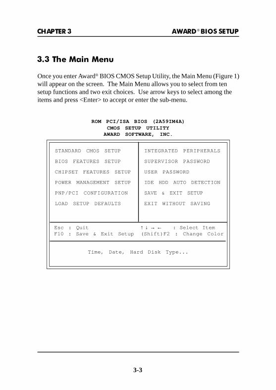
3.3 The Main Menu
Once you enter Award® BIOS CMOS Setup Utility, the Main Menu (Figure 1)will appear on the screen. The Main Menu allows you to select from tensetup functions and two exit choices. Use arrow keys to select among theitems and press <Enter> to accept or enter the sub-menu.
ROM PCI/ISA BIOS (2A59IM4A)CMOS SETUP UTILITY
AWARD SOFTWARE, INC.
STANDARD CMOS SETUP
BIOS FEATURES SETUP
CHIPSET FEATURES SETUP
POWER MANAGEMENT SETUP
PNP/PCI CONFIGURATION
LOAD SETUP DEFAULTS
INTEGRATED PERIPHERALS
SUPERVISOR PASSWORD
USER PASSWORD
IDE HDD AUTO DETECTION
SAVE & EXIT SETUP
EXIT WITHOUT SAVING
Esc : QuitF10 : Save & Exit Setup
Time, Date, Hard Disk Type...
↑ ↓ → ← : Select Item(Shift)F2 : Change Color

CHAPTER 3 AWARD® BIOS SETUP
3-4
Standard CMOS SetupThis setup page includes all the items in a standard compatible
BIOS.
BIOS Features SetupThis setup page includes all the items of Award® special enhanced
features.
Chipset Features SetupThis setup page includes all the items of chipset special features.
Power Management SetupThis category determines the power consumption for system after
setting the specified items. Default value is Disable.
PCI Configuration SetupThis category specifies the IRQ level for PCI and ISA devices.
Supervisor Password/User PasswordChange set or disable password. This function allows the user
access to the system and setup or just setup.
Load Setup DefaultsChipset defaults indicates the values required by the system for the
maximum performance.
IDE HDD Auto DetectionAutomatically configure hard disk parameters.
Save & Exit SetupSave CMOS value changes to CMOS and exit setup.
Exit Without SavingAbandon all CMOS value changes and exit setup.

CHAPTER 3 AWARD® BIOS SETUP
3.4 Standard CMOS Setup
The items in Standard CMOS Setup Menu are divided into 10categories. Each category includes no, one or more than one setup items.Use the arrow keys to highlight the item and then use the <PgUp> or<PgDn> keys to select the value you want in each item.
ROM PCI/ISA BIOS (2A59IM4A)STANDARD CMOS SETUP
AWARD SOFTWARE, INC.
HARD DISKS TYPE SIZE CYLS HEADS PRECOMP LANDZONE SECTORMODE
Primary Master: Auto 0 0 0 0 0 0 AUTO
Primary Slave : Auto 0 0 0 0 0 0 AUTO
Secondary Master : Auto 0 0 0 0 0 0 AUTO
Secondary Slave : Auto 0 0 0 0 0 0 AUTO
Drive A : 1.44M,3.5in. Base Memory: 640KDrive B : None Extended Base Memory:15360K
Other Memory: 384KVideo : EGA/VGAHalt On : All, but Keyboard Total Memory: 16384K
Date(mm:dd:yy): Fri, Feb 28,1997Time(hh:mm:ss): 00:00:00
ESC : Quit ↑ ↓ → ← : Select Item PU/PD/+/- : Modify
F1 : Help (Shift)F2 : Change Color
3-5

CHAPTER 3 AWARD® BIOS SETUP
DateThe date format is <day><month> <date> <year>.
Day Day of the week, from Sun to Sat, determined byBIOS. Read-only.
month The month from Jan. through Dec.date The date from 1 to 31 can be keyed by numeric
function keys.year The year, depends on the year of the BIOS
TimeThe time format is <hour> <minute> <second>.
PrimaryMaster/PrimarySlaveSecondaryMaster/Secondary Slave
These categories identify the types of 2 channels that have beeninstalled in the computer. There are 45 pre-defined types and 4 user defin-able types for Enhanced IDE BIOS. Type 1 to Type 45 are pre-defined. TypeUser is user-definable.
Press PgUp/<+> or PgDn/<-> to select a numbered hard disk type ortype the number and press <Enter>. Note that the specifications of yourdrive must match with the drive table. The hard disk will not work properly ifyou enter improper information for this category. If your hard disk drivetype is not matched or listed, you can use Type User to define your owndrive type manually.
If you select Type User, related information is asked to be entered tothe following items. Enter the information directly from the keyboard andpress <Enter>. This information should be provided in the documentationfrom your hard disk vendor or the system manufacturer.
3-6

CHAPTER 3 AWARD® BIOS SETUP
If the controller of HDD interface is ESDI, the selection shall be“Type 1”.
If the controller of HDD interface is SCSI, the selection shall be“None”.
If the controller of HDD interface is CD-ROM, the selection shall be“None”.
CYLS. number of cylindersHEADS number of headsPRECOMP write precomLANDZONE landing zoneSECTORS number of sectorsMODEHDD access mode
3-7

CHAPTER 3 AWARD® BIOS SETUP
3.5 BIOS Features Setup
ROM PCI/ISA BIOS (2A59IM4A)BIOS FEATURES SETUP
AWARD SOFTWARE, INC.
Virus WarningDuring and after the system boots up, any attempt to write to the
boot sector or partition table of the hard disk drive will halt the system andthe following error message will appear. For the meantime, you can run ananti-virus program to locate the problem.
!WARNING!Disk Boot Sector is to be modified
Type “Y” to accept write or “N” to abort writeAward Software, Inc.
Virus Warning : Disabled Video BIOS Shadow :EnabledCPU Internal Cache : Enabled C8000-CBFFF Shadow :DisabledExternal Cache : Enabled CC000-CFFFF Shadow :DisabledQuick Power on Self Test : Disabled D0000-D3FFF Shadow :DisabledBoot Sequence : A,C,SCSI D4000-D7FFF Shadow :DisabledSwap Floppy Drive : Disabled D8000-DBFFF Shadow :DisabledBoot up Floppy Seek : Enabled DC000-DFFFF Shadow :DisabledBoot up NumLock status : OnBoot up System Speed : HighTypematic Rate Setting : DisabledTypematic Rate(char/sec) : 6Typematic Delay(Msec) : 250Security Option : SetupPCI/VGA palette snoop : DisabledOS select for DRAM>64MB : Non-OS2
Esc : Quit ↑ ↓ → ← : Select item
F1 : Help PU/PD/+/- : modify
F5 : Old Value(Shift) F2 : Color
F6 : Load BIOS Defaults
F7 : Load Setup Defaults
3-8

CHAPTER 3 AWARD® BIOS SETUP
Disabled (default) No warning message to appear when anythingattempts to access the boot sector or hard diskpartition table.
Enabled Activates automatically when the system bootsup causing a warning message to appear whenanything attempts to access the boot sector ofhard disk partition table.
Note: This function is available only for DOS and other OS that do nottrap INT13.
CPU Internal CacheThe default value is Enabled. If your CPU is without Internal Cache
then this item “CPU Internal Cache” will not be shown.
Enabled (default) Enable cacheDisabled Disable cache
Note: The internal cache is built in the processor.
CPU External CacheChoose Enabled or Disabled. This option enables the level 2 cache
memory.
Quick Power On Self TestThis category speeds up Power On Self Test (POST) after you
power on the computer. If this is set to Enabled, BIOS will shorten or skipsome check items during POST.
Enabled Enable quick POSTDisabled (default) Normal POST
3-9

CHAPTER 3 AWARD® BIOS SETUP
Boot SequenceThis category determines which drive the computer searches first
for the disk operating system (i.e., DOS). The settings are A,C,SCSI/C,A,SCSI/C,CD-ROM,A/CD-ROM,C,A/D,A,SCSI/E,A,SCSI/F,A,SCSI/SCSI,A,C/SCSI,C,A/C only. Default value is A,C,SCSI.
Swap Floppy DriveSwitches the floppy disk drives between being designated as A
and B. Default is Disabled.
Boot Up Floppy SeekDuring POST, BIOS will determine if the floppy disk drive installed
is 40 or 80 tracks. 360K type is 40 tracks while 720K, 1.2M and 1.44M are all80 tracks.
Enabled(default) BIOS searches for floppy disk drive to determineif it is 40 or 80 tracks. Note that BIOS cannot tell from 720K, 1.2M or 1.44M drive type asthey are all 80 tracks.
Disabled BIOS will not search for the type of floppy diskdrive by track number. Note that there will notbe any warning message if the drive installed is360K.
Boot Up NumLock StatusThe default value is On.
On (default) Keypad is numeric keys.Off Keypad is arrow keys.
Boot Up System SpeedThis selects the speed that the system will run at immediately after
power up.
High (default) Sets the speed to high.Low Sets the speed to low.
3-10

CHAPTER 3 AWARD® BIOS SETUP
Gate A20 OptionNormal The A20 signal is controlled by keyboard
controller or chipset hardware.Fast(default) Default : Fast. The A20 signal is controlled by
Port 92 or chipset specific method.
Typematic Rate SettingThis determines the typematic rate.
Enabled Enable typematic rate and typematic delayprogramming.
Disabled(default)Disable typematic rate and typematic delayprogramming. The system BIOS will use defaultvalue of this 2 items and the default is controlledby keyboard.
Typematic Rate (Chars/Sec)6 (default) 6 characters per second8 8 characters per second10 10 characters per second12 12 characters per second15 15 characters per second20 20 characters per second24 24 characters per second30 30 characters per second
Typematic DelayChoose the length of delay from the time you press a key and the
character starts repeating. (Units are mil-secs)
3-11

CHAPTER 3 AWARD® BIOS SETUP
3-12
Security OptionThis category allows you to limit access to the system and Setup,
or just to Setup.
System The system will not boot and access to Setupwill be denied if the correct password is notentered at the prompt.
Setup(default) The system will boot, but access to Setup willbe denied if the correct password is not enteredat the prompt.
PCI VGA Palette SnoopingChoose Disabled or Enabled. Some graphic controllers which are
not VGA compatible, take the output from a VGA controller and map it totheir display as a way to provide the boot information and the VGAcompatibility.
However, the color information coming from the VGA controller isdrawn from the palette table inside the VGA controller to generate the propercolors, and the graphic controller needs to know what is in the palette of theVGA controller. To do this, the non-VGA graphic controller watches for theWrite access to the VGA palette and registers the snoop data. In PCI basedsystems, where the VGA controller is on the PCI bus and a non-VGA graphiccontroller is on an ISA bus, the Write Access to the palette will not show upon the ISA bus if the PCI VGA controller responds to the Writes.
In this case, the PCI VGA controller should not respond to the Write.It should only snoop the data and permit the access to be forwarded to the ISAbus. The non-VGA ISA graphic controller can then snoop the data on the ISAbus. Unless you have the above situation, you should disable this option.
Disabled (default) Disables the functionEnabled Enables the function
OS Selection for DRAM > 64MBAllows OS/2® to be used with > 64 MB of DRAM. Settings are
Non-OS/2® (default) and OS/2®. Set to OS/2® if using more than 64MB andrunning OS/2®.
CHAPTER 3 AWARD® BIOS SETUP
Video BIOS ShadowDetermines whether video BIOS will be copied to RAM for faster
execution. Video shadow will increase the video performance.
Enabled (default) Video shadow is enabledDisabled Video shadow is disabled
C8000 - CFFFF Shadow/E8000 - EFFFF ShadowDetermines whether the optional ROM will be copied to RAM for
faster execution.
Enabled Optional shadow is enabledDisabled (default) Optional shadow is disabled
Note: For C8000-DFFFF optional-ROM on PCI BIOS , BIOS will automati-cally enable the shadow RAM. User does not have to select theitem.
3-13

CHAPTER 3 AWARD® BIOS SETUP
Auto Configuration :Enabled
DRAM Timing : 70ns
DRAM Leadoff Timing : 10/6/4
DRAM Read Burst (EDO/FP) : x333/x444
DRAM Write Burst Timing : x333
Fast EDO Lead Off : Disabled
Refresh RAS# Assertion :3
Fast RAS to CAS Delay :3
DRAM Page IDLE Timer :2
DRAM Enhanced Paging : Enabled
Fast MA to RAS# Delay :2 Clks
SDRAM (CAS Lat/RAS-to-CAS):3/3
SDRAM Speculative Read : Disabled
System BIOS Cacheable : Disabled
Video BIOS Cacheable : Disabled
8 Bit I/O Recovery Time :1
16 Bit I/O Recovery Time :2
Memory Hole at 15M-16M : Disabled
PCI 2.1 compliance :Disabled
3.6 Chipset Features Setup
The Chipset Features Setup option is used to change the values ofthe chipset registers. These registers control most of the system options inthe computer.
Choose the “CHIPSET FEATURES SETUP” from the Main Menuand the following screen will appear.
ROM PCI/ISA BIOS(2A59IM4A)CMOS SETUP UTILITY
CHIPSET FEATURES SETUP
Note: Change these settings only if you are familiar with the chipset.
Esc : Quit ↑ ↓ → ← : Select item
F1 : Help PU/PD/+/- : modify
F5 : Old Value(Shift) F2 : Color
F6 : Load BIOS Defaults
F7 : Load Setup Defaults
3-14

CHAPTER 3 AWARD® BIOS SETUP
Auto ConfigurationChoosing Enabled (default) will automatically configure chipset
features using default settings. Choose Disable to customize setup.
DRAM TimingSets the DRAM speed at 70ns (default) or 60ns. It will set the
speed of the EDO/FP DRAM.
DRAM Leadoff TimingTo be able to change the setting, Auto configuration must be
disable. If the Bus Clock is 75MHz set it to 11/7/4, and if the Bus Clock is 66/60/55 MHz set it to 10/6/4. Default setting is 10/6/4.
DRAM Read Burst (EDO/FP)Under Auto config. the BIOS will identify which type of DRAM is
being used. Choose the setting accordingly. To customize, use this optionwhich sets the Read Burst time for accessing the DRAM. The timing useddepends on the type of DRAM and access time being used. The settings arex222/x333, x333/x444, or x444/x444.
Note: If the user chooses DRAM Read Burst (EDO/FP): x333/x444 it signi-fies that:a. 60ns EDO with 75 MHz Bus Clock is set at x333, if the Bus Clock is 66/60/55 MHz, then it is set at x222.b. 60ns FP with 75 MHz is set at x444, if the Bus Clock is 66/60/55,
then it is set at x333.c. 70ns EDO and FP DRAM must increase the burst time. So you must set x222 to x333 and x333 to x444.
DRAM Write Burst TimingThis option chooses the Write Burst Timing for accessing DRAM.
See: DRAM Read Burst Option. Choose x222/x333/x444.
3-15

CHAPTER 3 AWARD® BIOS SETUP
Fast EDO Lead OffUnder Auto config. the BIOS will identify which type of DRAM is
being used. Choose the setting accordingly. To customize, use this option.Choose Enable or Disable. If the system is using EDO DRAM, chooseenable. But if the system is using both EDO and FP DRAM, choose Disable.
Refresh RAS# AssertionThe settings are 4 Clks or 5 Clks. Using 60 ns DRAM at 75 Mhz Bus
Clock must be set to 5 Clks, while 66/60/55 Mhz Bus Clock must be set to 4Clks. But if you use 70 ns DRAM, it must be set to 5 Clks.
Fast RAS to CAS DelayThe settings are 2 or 3. 2 RAS to CAS delay is set to 2 clock, while
3 RAS to CAS delay is set to 3 clock. The clock is dependent with theDRAM Timing and Bus Clock.
DRAM Page IDLE TimerThe settings are 2 Clks, 4 Clks, 6Clks, or 8 Clks. Default settings is 2
Clks.
DRAM Enhanced PagingChoose Enable(default) or Disable.
Fast MA to RAS# DelayThe settings are 1 Clks or 2 Clks(default). During 1T, one bus clock
is allowed, while 2T allows two bus clock for MA address setup time toRAS assertion. This is also dependent on DRAM Timing.
SDRAM (CAS Lat/RAS-to-CAS)The settings are 3/3 or 2/2. This option is for SDRAM CAS latency
time and RAS# to CAS# delay time. The default setting is 3/3.
3-16

CHAPTER 3 AWARD® BIOS SETUP
SDRAM Speculative ReadThe settings are enable or disable. If you only use One Bank for
SDRAM and there’s no EDO or FP mix together, the setting is Enable. If twobanks are used by SDRAM, it will automatically be set to disable. Thedefault setting is enable.
System BIOS CacheableBy choosing Disabled (default) the system BIOS will be shadowed
into DRAM only. Enabled will have the system BIOS shadowed andcacheable.
Video RAM CacheableSame as system BIOS Cacheable
8-bit I/O recovery time: 1/2/3/4/5/6/7/NA16-bit I/O recovery time: 1/2/3/NA
Choose the recovery time for 8-bit and 16-bit I/O cyclesrespectively.
Note: NA is not available and so the recovery time of 3.5 SYSCLK will beinserted.
Memory Hole At 15M-16MChoosing Enabled will enable a memory hole in the DRAM space.
The CPU cycle matching the enabled hole will be passed on to the PCI. PCIcycles matching an enabled hole are ignored. Disabled (default) will disablethis function.
Note: A selected (Enabled) hole is not remapped.
PCI 2.1 ComplianceThe Settings are Enable or Disable. During Enable, those PCI add-
on cards with PCI 2.1 compliance will perform better. But some PCI carddoes not meet PCI 2.1 compliance, so the default setting is Disabled.
3-17

CHAPTER 3 AWARD® BIOS SETUP
3.7 Power Management Setup
The Power Management Setup will appear on your screen like this:
ROM PCI/ISA BIOS (2A59IM4A)POWER MANAGEMENT SETUP
AWARD SOFTWARE, INC.
Power ManagementThis category determines the power consumption for system after
selecting below items. Default value is Disable. The following pages tellyou the options of each item & describe the meanings of each options.
** Reload Global Timer Events **IRQ [3-7,9-15],NMI : EnabledPrimary IDE 0 : EnabledPrimary IDE 1 : DisabledSecondary IDE 0 : DisabledSecondary IDE 1 : DisabledFloppy Disk : EnabledSerial Port : EnabledParallel Port : Enabled
Power Management :User DefinePM Control by APM :YesVideo Off Method :DPMSVideo Off After :StandbyDoze Mode :DisabledStandby Mode :DisabledSuspend Mode :DisabledHDD Power Down :DisabledThrottle Duty Cycle :62.5%VGA Active Monitor :EnabledSoft-Off by PWR-BTTN :Delay 4secCPUFAN Off In Suspend :EnabledResume by Ring :DisabledResume by Alarm :DisalbedDate(of Month) Alarm :5Time(hh:mm:ss) Alarm :11:00:00
** Break Event From Suspend **
IRQ 8 Clock Event : Disabled
Esc : Quit ↑ ↓ → ← : Select item
F1 : Help PU/PD/+/- : modify
F5 : Old Value(Shift) F2 : Color
F6 : Load BIOS Defaults
F7 : Load Setup Defaults
3-18

CHAPTER 3 AWARD® BIOS SETUP
Power ManagementDisable Global Power Management will be
disabled.User Define Users can configure their own power
management.Min Saving Pre-defined timer values are used such
that all timers are in their MAX value.Max Saving Pre-defined timer values are used such
that all timers are in their MIN value.
PM Control by APMNo System BIOS will ignore APM when
power managing the system.Yes System BIOS will wait for APM’s
prompt before it enter any PM mode
Note :Enable this for O.S. with APM like Windows® 95, Windows® NT, etc.
Video Off MethodBlank Screen The system BIOS will only blank off
the screen when disabling video.V/H SYN C+Blank In addition to (1), BIOS will also turn
off the V-SYNC & H-SYNC signalsfrom VGA card to monitor.
DPMS This function is enabled only for VGAcard supporting DPMS.
Note: Green monitors detect the V/H SYNC signals to turn off its electrongun.
3-19

CHAPTER 3 AWARD® BIOS SETUP
Doze ModeDisable System will never enter DOZE mode.
1 Min/2 Min/4 Min/6 Min/8 Min/10 Min/20 Min/30 Min/40 Min/1 Hr
Standby Mode Disable System will never enter STANDBY mode.
1 Min/2 Min/4 Min/6 Min/8 Min/10 Min/20 Min/30 Min/40 Min/1 Hr
Video Off AfterThe settings are N/A, Standby, Doze, or Suspend. This option is for
choosing the setting in which the monitor will turn off.N/A Always turn on.Doze During Doze mode, the monitor will be turned off.Standby During Standby mode, the monitor will be turned off.Suspend During Suspend mode, the monitor will be turned off.The default setting is Standby.
Defines the continuous idle time before thesystem enters STANDBY mode.If any item defined in the options of “PowerDown and Resume events” is enabled & active,STANDBY timer will be reloaded. When thesystem has entered Standby mode , any of theitems that are enabled in “Wake Up Events ofDoze and Standby” will trigger the system towake up.
Defines the continuous idle time before thesystem enters DOZE mode.If any item defined in the options of “PowerDown and Resume events” is enabled & active,DOZE timer will be reloaded. When the systemhave entered Doze mode, any of the itemsenabled in “Wake Up Events in Doze andStandby” will trigger the system to wake up.
3-20

CHAPTER 3 AWARD® BIOS SETUP
HDD Power DownDisable HDD’s motor will not shut off.
1 Min/2 Min/3 Min/4 Min/5 Min/6 Min/7 Min/8 Min/ 9 Min/10 Min/11 Min/12 Min/13 Min/14 Min/15 Min
Throttle Duty CycleThis option will determine how much power will be used by the
CPU , if the system goes into suspend mode.
VGA Active MonitorDuring Enabled, if there’s no activity in the monitor screen the
system will go into Power Saving Mode. During Disabled, the system willgo into Power Saving Mode, whether there is activity in the monitor screenor not. The settings are Disabled and Enabled.
Suspend ModeDisable System will never enter SUSPEND mode.
1 Min/2 Min/4 Min/6 Min/8 Min/10 Min/20 Min/30 Min/40 Min/1 Hr
Defines the continuous idle time before thesystem enters SUSPEND mode.If any item defined in the options of “PowerDown & Resume Events” is enabled & active,SUSPEND timer will be reloaded. When thesystem has entered SUSPEND mode, any of theitems enabled in the “Power Down & ResumeEvents” will trigger the system to wake up.
Defines the continuous HDD idle time beforethe HDD enters the power saving mode (motoroff). BIOS will turn off the HDD’s motor whentime is out.
3-21
CHAPTER 3 AWARD® BIOS SETUP
Soft-Off by PWR-BTTNThe settings are Delay 4 sec or Instant-off. During Delay 4 sec, if
you push the switch one time, the system goes into suspend mode and ifyou push it more than 4 second, the system will be turned off. Duringinstant-off, the system will turn off once you push the switch.
CPUFAN Off In SuspendDuring Enabled, if the system goes into suspend mode, the CPU
fan will stop. During Disabled, if the system goes into suspend mode theCPU fan will not stop.
Note: Only JFAN1 has this function.
Resume by RingDuring Disabled, the system will ignore any incoming call from the
modem. During Enabled, the system will boot up if there’s an incoming callfrom the modem.
Note: If you have change the setting, you must let the system boot up untilit goes to the operating system, before this function will work.
Resume by AlarmThis function is for setting date and time for your computer to boot
up. During Disabled, you cannot use this function. During Enabled, choosethe Date and Time Alarm:
Date(of month) Alarm You can choose which month thesystem will boot up.
Time(hh:mm:ss) Alarm You can choose what hour, minute andsecond the system will boot up.
Note: If you have change the setting, you must let the system boot up untilit goes to the operating system, before this function will work.
3-22

CHAPTER 3 AWARD® BIOS SETUP
IRQ 8 Clock EventIRQ[3-7,9-15], NMI : EnabledPrimary IDE 0 : EnabledPrimary IDE 1 : DisabledSecondary IDE 0 : DisabledSecondary IDE 1 : DisabledFloppy Disk : EnabledSerial Port : EnabledParallel Port : Enabled
During Enabled, if any interrupt event occurs, the system will wake-up from suspend mode. During Disabled, the system will not monitor anyinterrupt event.
3-23

CHAPTER 3 AWARD® BIOS SETUP
3.8 PNP/PCI Configuration Setup
You can manually configure the PCI Device’s IRQ. The followingpages tell you the options of each item & describe the meanings of eachoptions.
ROM PCI/ISA BIOS (2A69HM4D)PNP/PCI CONFIGURATION SETUP
AWARD SOFTWARE, INC.
PnP OS InstalledWhen set to YES, BIOS will only initialize the PnP cards used for
booting (VGA, IDE, SCSI). The rest of the cards will be initialized by the PnPoperating system like Windows® 95. When set to NO, BIOS will initialize allthe PnP cards. So, for non-PnP operating system (DOS, Netware®), thisoption must set to NO.
PnP OS Installed :No
Resources Controlled By :Auto
Reset Configuration Data :Disabled
IRQ-3 assigned to :Legacy ISA
IRQ-4 assigned to :Legacy ISA
IRQ-5 assigned to :PCI/ISA PnP
IRQ-7 assigned to :PCI/ISA PnP
IRQ-9 assigned to :PCI/ISA PnP
IRQ-10assigned to :PCI/ISA PnP
IRQ-11assigned to :PCI/ISA PnP
IRQ-12assigned to :PCI/ISA PnP
IRQ-14assigned to :PCI/ISA PnP
IRQ-15assigned to :PCI/ISA PnP
DMA-0assigned to :PCI/ISA PnP
DMA-1assigned to :PCI/ISA PnP
DMA-3assigned to :PCI/ISA PnP
DMA-5assigned to :PCI/ISA PnP
DMA-6assigned to :PCI/ISA PnP
DMA-7assigned to :PCI/ISA PnP
PCI IDE IRQ Map To : PCI-Auto
Primary IDE INT# : A
Secondary IDE INT# : B
Assign IRQ for VGA : Disabled
Used MEM base addr : C800
Used MEM Length : 8K
Esc : Quit ↑ ↓ → ← : Select item
F1 : Help PU/PD/+/- : modify
F5 : Old Value(Shift) F2 : Color
F6 : Load BIOS Defaults
F7 : Load Setup Defaults
3-24
CHAPTER 3 AWARD® BIOS SETUP
Resources Controlled ByBy Choosing “Auto”, the system BIOS will detect the system
resource and automatically assign the relative IRQ and DMA Channel foreach peripheral.
By Choosing “Manual”(default), the user will need to assign IRQ &DMA for add-on cards. Be sure that there is no conflict for IRQ/DMA and I/O ports.
Note: When choosing “Auto” you must be sure that all of the systemadd-on cards are PnP type.
Reset Configuration DataThe system BIOS supports the PnP feature so the system needs to
record which resource is assigned and protect resources from conflict.Every peripheral device has a node which is called ESCD. This node recordswhich resources are assigned to it. The system needs to record and updateESCD to the memory locations. These locations (4K) are reserved at thesystem BIOS.
If Disabled (default) is chosen the system’s ESCD will update onlywhen the new configuration varies from the last one.
If Enabled is chosen the system will be forced to update thesystem’s ESCD. Then, this option willbe auto-set to Disable.
IRQ-3 assigned to : Legacy ISAIRQ-4 assigned to : Legacy ISAIRQ-5 assigned to : PCI/ISA PnPIRQ-7 assigned to : Legacy ISAIRQ-9 assigned to : PCI/ISA PnPIRQ-10 assigned to : PCI/ISA PnPIRQ-11 assigned to : PCI/ISA PnPIRQ-12 assigned to : PCI/ISA PnPIRQ-14 assigned to : PCI/ISA PnP
3-25

CHAPTER 3 AWARD® BIOS SETUP
3-26
IRQ-15 assigned to : PCI/ISA PnPDMA-0 assigned to : PCI/ISA PnPDMA-1 assigned to : PCI/ISA PnPDMA-3 assigned to : PCI/ISA PnPDMA-5 assigned to : PCI/ISA PnPDMA-6 assigned to : PCI/ISA PnPDMA-7 assigned to : PCI/ISA PnP
The above settings will be shown on the screen only if “Manual” ischosen for the Resources Controlled By function.
Legacy is the term which signifies that a resource is assigned to theISA Bus and provides for non PnP ISA add-on card. PCI/ISA PnP signifiesthat a resource is assigned to the PCI Bus or provides for ISA PnP add-oncards and peripherals.
PCI IDE IRQ Map ToPCI-Auto: This setting is for off-board PCI IDE card and is
fully compatible with PCI specifications.
PCI-Slot 1-5: This setting is used if off-board PCI IDE card isnot fully compatible with PCI specifications.You must specify which PCI slot the PCI IDECard is installed in.
ISA: This setting is used if the off-board PCI IDEcard uses an edge trigger and IRQ routesdirectly to the ISA Bus.
Note: The user will need to disable the on-board on-chipset PCI IDEcontroller when installing off-board PCI IDE add-on cards. (See theINTEGRATED PERIPHERALS SETUP) These two options choosethe primary and secondary IDE Channel interrupts when the userinstalls off-board PCI IDE add-on cards.

CHAPTER 3 AWARD® BIOS SETUP
Assign IRQ for VGALets the user choose which IRQ to assign for VGA card.
Used MEM base addrLets the user choose the Legacy ISA addr. The settings are NA#,
C800, CC00, D000, D400, D800 OR DC00.
Used MEM LengthChoose 8K, 16K, 32K, or 64K MEM length for the MEM used by
the Legacy ISA address.
3-27
3.9 Load BIOS/Setup Defaults
This Main Menu item loads the default system values. If the CMOSis corrupted the defaults are loaded automatically. Choose this item and thefollowing message appears:
“ Load Setup Defaults (Y / N) ? N “
To use the Setup defaults, change the prompt to “Y” and press < Enter >
Note: The Setup defaults can be customized to increase performance.However the BIOS defaults can always be used as a back up if there
is some problem with the mainboard operation.

CHAPTER 3 AWARD® BIOS SETUP
3.10 Integrated Peripherals
ROM PCI/ISA BIOS (2A69HM4D)INTEGRATED PERIPHERALS
AWARD SOFTWARE, INC.
IDE HDD Block ModeEnabled/DisabledEnabled allows the Block mode access for the
IDE HDD.
IDE Primary Master PIOAuto/Mode0/Mode1-4
IDE Primary Slave PIOAuto/Mode0/Mode1-4
IDE Secondary Master PIOAuto/Mode0/Mode1-4
IDE HDD Block Mode : Enabled
IDE Primary Master PIO : Auto
IDE Primary Slave PIO : Auto
IDE Secondary Master PIO : Auto
IDE Secondary Slave PIO : Auto
IDE Primary Master UDMA : Auto
IDE Primary Slave UDMA : Auto
IDE Secondary Master UDMA: Auto
IDE Secondary Slave UDMA : Auto
On-Chip Primary PCI IDE : Enabled
On-Chip Primary PCI IDE : Enabled
USB Keyboard Controller :Disabled
Onboard FDD controller : Enabled
Onboard Serial Port 1 : 3F8/IRQ4
Onboard Serial Port 2 : 2F8/IRQ3
UART 2 Mode : ASKIR
IR Function Duplex : Half
RxD , TxD Active :Hi , Hi
Onboard Parallel Port : 378H/IRQ7
Esc : Quit ↑ ↓ → ← : Select item
F1 : Help PU/PD/+/- : modify
F5 : Old Value(Shift) F2 : Color
F6 : Load BIOS Defaults
F7 : Load Setup Defaults
Onboard Parallel Mode : ECP/EPP
ECP Mode Use DMA :3
Parallel Port EPP Type :EPP1
3-28
CHAPTER 3 AWARD® BIOS SETUP
IDE Secondary Slave PIOAuto/Mode0/Mode1-4
For these 4 IDE options, choose “Auto” to have the system BIOSauto detect the IDE HDD operation mode for PIO access.
Note: Some IDE HDD can not operate at the responding HDD’s mode.When the user has selected “Auto” and the system BIOS hasaccepted the HDD response mode, the user may degrade theHDD’s operation mode. Ex: IF the HDD reported it can operate inmode 4 but it is not operating properly, the user will have tomanually change the operation mode to mode 3.
Choosing Mode 1-4 will have the system ignore the HDD’s reportedoperation mode and use the selected mode instead.
Note: According to ATA specs. Mode 4 transfer rate is > Mode 3 > Mode 2> Mode 1 > Mode 0. If the user ’s HDD can operate at Mode 3 theuser can also select a slower Mode (i.e. Mode 0-2) but not a fasterMode (ie Mode 4).
On-Chip Primary PCI IDEEnabled/Disabled
On-Chip Secondary PCI IDEEnabled/Disabled The system provides for a On-Board
On-Chipset PCI IDE controller thatsupports Dual Channel IDE (Primaryand Secondary). A maximum of 4 IDEdevices can be supported. If the userinstall the Off-Board PCI IDE controller(i.e. add-on cards), the user mustchoose which channels will be disabled.This will depend on which channel willbe used for the Off-Board PCI IDE add-on card.
3-29

CHAPTER 3 AWARD® BIOS SETUP
PCI Slot IDE 2nd ChannelEnabled/Disabled Choosing Enabled will allow the system
to access the 2nd IDE channel without adevice driver. If the Off-Board PCI IDEadd-on card is installed, the 2nd IDEchannel will need to be used.
Onboard FDD ControllerEnabled/Disabled The system has an on-board Super I/O
chip with a FDD controller that supports2 FDDs for 360K/720K/1.2M/1.44M/2.8M. Choose “Enabled” to use the on-board FDD controller for accessing theFDD. Otherwise choose “Disabled” touse the off-board FDD controller.
Onboard Serial Port 1Disabled/(3F8/IRQ4)/(2F8/IRQ3)/ (3E8/IRQ4)/(2E8/IRQ3)
Onboard Serial Port 2Disabled/(3F8/IRQ4)/(2F8/IRQ3)/(3E8/IRQ4)/(2E8/IRQ3)The system has an On-board Super I/O chipset with 2 serial ports.
The On-board serial ports can be selected as:
Disabled3F8/IRQ4 COM 1 uses IRQ42F8/IRQ3 COM 2 uses IRQ33E8/IRQ4 COM 3 uses IRQ42E8/IRQ3 COM 4 uses IRQ4
Note: Because the ISA Bus Interrupt accepts low to high edge trigger, theinterrupt request line cannot be shared by multiple sources. If an off-board ISA add-on card with a serial port is installed the user may haveto disable the on-board serial port because it will conflict with IRQrequest line for the off-board serial port.
3-30
CHAPTER 3 AWARD® BIOS SETUP
UART 2 MODEStandard/ASKIR/ The system’s built-in IR (Infrared) is on
the on-board Super I/O chipset and itshares serial port 2 with UART 2. Onlyone option can be selected for serial port2, either the IR or UART. Selecting theIR mode will prompt the followingmessage:
IR Function DuplexHalf/Full Users can choose between operating
the IR in Half duplex or Full duplexmode. Half duplex designates one IR asa receiver and one as a transmitter.Fullduplex mode designates that the twoIRs receive and transmit data togethersimultaneously.
RxD , TxD ActiveHi-Hi/Hi-Lo/ The user can choose between the
preceding RxD (Receive Data), TxD(Transmit Data) activity levels.
Onboard Parallel PortDisabled/ There is a built-in parallel port on the
on-board Super I/O chipset thatprovides Standard, ECP, and EPPfeatures. It has the following options:
Disable3BCH/IRQ7 Line Printer port 0278H/IRQ5 Line Printer port 2378H/IRQ5 Line Printer port 1
3-31
Lo-Hi/Lo-Lo
(3BCH/IRQ7)/(278H/IRQ5)/(378H/IRQ5)

CHAPTER 3 AWARD® BIOS SETUP
SPP/(EPP/SPP)/ECP(ECP/EPP)
Onboard Parallel ModeSPP : Standard Parallel PortEPP : Enhanced Parallel PortECP : Extended Capability Port
To operate the onboard parallel port asStandardParallel Port only, choose“SPP.” To operate the onboard parallelport in the ECP and SPP modes simulta-neously choose “ECP/SPP.” Bychoosing “ECP”, the onboard parallelport will operate in ECP mode only.Choosing “ECP/EPP” will allow theonboard parallel port to support both theECP and EPP modes simultaneously.The ECP mode has to use the DMAchannel, so choose the onboard parallelport with the ECP feature. After select-ing it, the following message will appear:“ECP Mode Use DMA” At this time theuser can choose between DMAchannels 3 or 1. The onboard parallelport is EPP Spec. compliant, so after theuser chooses the onboard parallel portwith the EPP function, the followingmessage will be displayed on the screen:“Parallel Port EPP Type.” At this timeeither EPP 1.7 spec. or EPP 1.9 spec. canbe chosen.
USB Controller Enabled/Disabled Choosing Enabled, will enable the on-
board USB port.
3-32

CHAPTER 3 AWARD® BIOS SETUP
3.11 Supervisor/User Password Setting
This Main Menu item lets you configure the system so that apassword is required each time the system boots or an attempt is made toenter the Setup program. Supervisor Password allows you to change allCMOS settings but the User Password setting doesn’t have this function.The way to set up the passwords for both Supervisor and User are as follow:
1. Choose “Change Password” in the Main Menu and press <Enter>.The following message appears:
“Enter Password:”
2. The first time you run this option, enter your password up to only 8characters and press <Enter>. The screen does not display the enteredcharacters. For no password just press <Enter>.
3. After you enter the password, the following message appears promptingyou to confirm the password:
“Confirm Password:”
4. Enter exactly the same password you just typed in to confirm the pass-word and press <Enter>.
5. Move the cursor to Save & Exit Setup to save the password.
6. If you need to delete the password you entered before, choose theSupervisor Password and press <Enter>. It will delete the password thatyou had before.
7. Move the cursor to Save & Exit Setup to save the option you did. Other-wise, the old password will still be there when you turn on your machinenext time.
3-33

CHAPTER 3 AWARD® BIOS SETUP
3.12 IDE HDD Auto Detection
You can use this utility to automatically detect the characteristics ofmost hard drives.
When you enter this utility, the screen asks you to select a specifichard disk for Primary Master. If you accept a hard disk detected by the BIOS,you can enter “Y” to confirm and then press <Enter> to check next hard disk.This function allows you to check four hard disks and you may press the<Esc> after the <Enter> to skip this function and go back to the Main Menu.
3-34
ROM ISA BIOSCMOS SETUP UTILITY
AWARD SOFTWARE, INC.
HARD DISKS TYPE SIZE CYLS HEADS PRECOMP LANDZONE SECTORMODE
Primary Master: Auto 0 0 0 0 0 0 AUTO
Primary Slave : Auto 0 0 0 0 0 0 AUTO
Secondary Master : Auto 0 0 0 0 0 0 AUTO
Secondary Slave : Auto 0 0 0 0 0 0 AUTO
Select Primary Master Option (N=Skip) : N
OPTIONS SIZE CYLS HEAD PRECOMP LANDZ SECTOR MODE
2 2112 1023 64 0 4094 63 LBA1 2113 4095 16 65535 4094 63 NORMAL3 2113 2047 32 65535 4094 63 LARGE
[ESC: Skip]

CHAPTER 4 AMI® BIOS USER�S GUIDE
Chapter 4
AMI® BIOS USER’s GUIDE
The system configuration information and chipset register information isstored in the CMOS RAM. This information is retained by a battery whenthe power is off. Enter the BIOS setup (if needed) to modify this information.
The following pages will describe how to enter BIOS setup, and all aboutoptions.
4-1
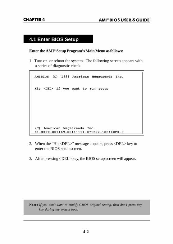
CHAPTER 4 AMI® BIOS USER�S GUIDE
2. When the “Hit <DEL>” message appears, press <DEL> key toenter the BIOS setup screen.
3. After pressing <DEL> key, the BIOS setup screen will appear.
AMIBIOS (C) 1996 American Megatrends Inc.
Hit <DEL> if you want to run setup
(C) American Megatrends Inc.61-XXXX-001169-00111111-071592-i82440FX-H
4.1 Enter BIOS Setup
Enter the AMI ® Setup Program’s Main Menu as follows:
1. Turn on or reboot the system. The following screen appears witha series of diagnostic check.
Note: If you don’t want to modify CMOS original setting, then don’t press any
key during the system boot.
4-2

CHAPTER 4 AMI® BIOS USER�S GUIDE
4. Use the <UP> and <DOWN> key to move the highlight scroll upor down.
5. Use the <ENTER> key to select the option.
6. To exit, press <ESC>. To save and exit, press <F10>.
7. Section 4.2 to 4.8 will explain the option in more details.
AMIBIOS HIFLEX SETUP UTILITIES - VERSION 1.07(C) 1996 American Megatrends, Inc. All Rights Reserved
Standard CMOS SetupAdvanced CMOS Setup
Advanced Chipset SetupPower Management Setup
PCI/Plug and Play SetupPeripheral Setup
Hardware Monitor SetupAuto-Detect Hard Disks
Change User PasswordChange Supervisor Password
Auto Configuration with Optimal SettingsAuto Configuration with Fail Safe Settings
Save Settings and ExitExit without Saving
Standard CMOS setup for changing time, hard disk type, etc.
4-3

CHAPTER 4 AMI® BIOS USER�S GUIDE
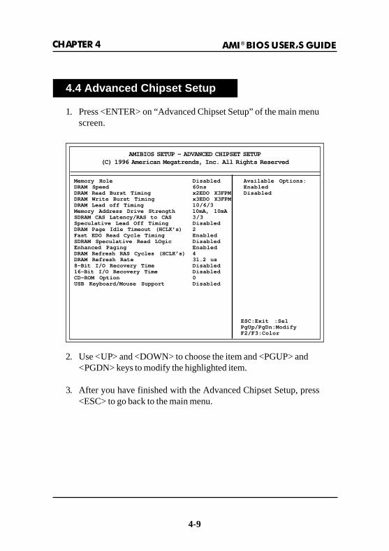
2. Use <UP> and <DOWN> to choose the item and <PGUP> and<PGDN> keys to modify the highlighted item.
3. After you have finished with the Standard CMOS Setup,press<ESC> to go back to the main menu.
4.2 Standard CMOS Setup
1. Press <ENTER> on “Standard CMOS Setup” of the main menuscreen .
AMIBIOS SETUP - STANDARD CMOS SETUP(C)1996 American Megatrends,Inc.All Rights Reserved
Date (mm/dd/yyyy): Fri June 20, 1997Time (hh/mm/ss): 17:09:25
Floppy Drive A: 1.44 MB 3 1/2Floppy Drive B: Not Installed
LBA Blk PIO 32BitType Size Cyln Head WPcom Sec Mode Mode Mode Mode
Pri Master : Auto ON ON AUTO ONPri Slave : Auto ON ON AUTO ONSec Master : Auto ON ON AUTO ONSec Slave : Auto ON ON AUTO ON
Boot Sector Virus Protection Disabled
ESC:Exit :SelPgUp/PgDn:ModifyF2/F3:Color
Time is 24 hour format:Hour: 00-23 Minute: 00-59 Second: 00-59(1:30AM = 01:30:00, 1:30PM = 13:30:00)
4-4
CHAPTER 4 AMI® BIOS USER�S GUIDE
2. Use <UP> and <DOWN> to choose the item and <PGUP> and<PGDN> keys to modify the highlighted item.
3. After you have finished with the Advanced CMOS Setup, press<ESC> to go back to the main menu.
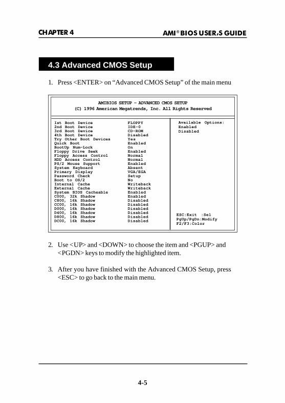
AMIBIOS SETUP - ADVANCED CMOS SETUP(C) 1996 American Megatrends, Inc. All Rights Reserved
Ist Boot Device FLOPPY2nd Boot Device IDE-03rd Boot Device CD-ROM4th Boot Device DisabledTry Other Boot Devices YesQuick Boot EnabledBootUp Num-Lock OnFloppy Drive Seek EnabledFloppy Access Control NormalHDD Access Control NormalPS/2 Mouse Support EnabledSystem Keyboard AbsentPrimary Display VGA/EGAPassword Check SetupBoot to OS/2 NoInternal Cache WritebackExternal Cache WritebackSystem BIOS Cacheable EnabledC000, 32k Shadow EnabledC800, 16k Shadow DisabledCC00, 16k Shadow DisabledD000, 16k Shadow DisabledD400, 16k Shadow DisabledD800, 16k Shadow DisabledDC00, 16k Shadow Disabled
Available Options:EnabledDisabled
ESC:Exit :SelPgUp/PgDn:ModifyF2/F3:Color
4.3 Advanced CMOS Setup
1. Press <ENTER> on “Advanced CMOS Setup” of the main menu
4-5

CHAPTER 4 AMI® BIOS USER�S GUIDE
Description of the item on screen follows:
1st Boot Device/2nd Boot Device/3rd Boot Device/4th Boot Device
This option sets the sequence of boot drives.The settings are:IDE0 The system will boot from the first HDD.IDE1 The system will boot from the Second HDD.IDE2 The system will boot from the Third HDD.IDE3 The system will boot from the Fourth HDD.F(optical) The system will boot from LS-120(120M Floppy).SCSI The system will boot from the SCSI.Network The system will boot from the Network drive.CD-ROM The system will boot from the CD-ROM.Disable Disable this sequence.
Try other Boot DevicesThis option sets the device boot, if all the Four Boot Devices failed.
Quick BootSet this option to Enabled to permit AMI® BIOS to boot within 5
seconds. This option replaces the old ABOVE 1 MB Memory Test option.The Optimal default setting is Enabled. The Fail-Safe default setting isDisabled.
Boot up Num LockWhen this option is set to Off, AMI® BIOS turns off the Num Lock
key when the system is powered on so the end user can use the arrow keyson both the numeric keypad and the keyboard. The settings are On or Off.The optimal default and Fail-Safe default settings are On.
Floppy Drive SeekWhen this option is set to Enabled, AMI® BIOS performs a Seek
command on floppy drive A: before booting the system. The settings areEnabled and Disabled. The Optimal and Fail-Safe default settings areDisabled.
4-6

CHAPTER 4 AMI® BIOS USER�S GUIDE
Floppy Access ControlThis option sets the Floppy to Read-only or Normal(Full Access).
HDD Access ControlThis option sets the HDD to Read-only or Normal(Full Access).
During Read-only, if you try to write on the HDD, the system will halt.
PS/2® Mouse SupportWhen this option is set to Enabled, AMI® BIOS will auto-detect the
presence of a PS/2® mouse and reserved an IRQ for the mouse. The settingsare Enabled and Disabled. The Optimal and Fail-Safe default settings areEnabled.
System Keyboard (leave on the default setting of Absent)
Primary DisplayThis option configures the primary display subsytem in the
computer. The settings are Mono(monochrome), 40CGA, 80CGA or VGA/EGA. The optimal and Fail-Safe default settings are VGA/EGA.
Password CheckThis option specifies the type of AMI® BIOS password protection
that is implemented. The Optimal and Fail-Safe default settings are Setup.
Boot to OS/2®
Set this option to Enabled only if your using an OS/2® and thememory size is 64MB.
Internal Cache/External CacheThis option Enabled or Disabled the Internal and the External
Cache.
4-7
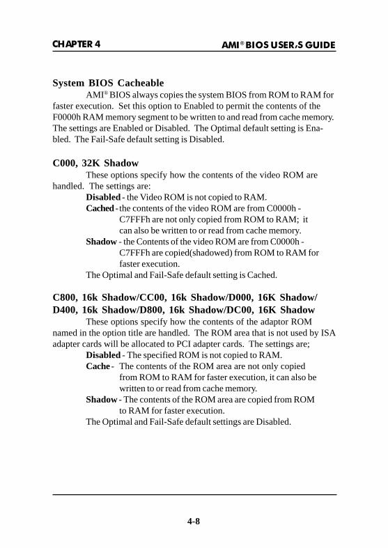
CHAPTER 4 AMI® BIOS USER�S GUIDE
System BIOS CacheableAMI ® BIOS always copies the system BIOS from ROM to RAM for
faster execution. Set this option to Enabled to permit the contents of theF0000h RAM memory segment to be written to and read from cache memory.The settings are Enabled or Disabled. The Optimal default setting is Ena-bled. The Fail-Safe default setting is Disabled.
C000, 32K ShadowThese options specify how the contents of the video ROM are
handled. The settings are:Disabled - the Video ROM is not copied to RAM.Cached - the contents of the video ROM are from C0000h -
C7FFFh are not only copied from ROM to RAM; itcan also be written to or read from cache memory.
Shadow - the Contents of the video ROM are from C0000h -C7FFFh are copied(shadowed) from ROM to RAM forfaster execution.
The Optimal and Fail-Safe default setting is Cached.
C800, 16k Shadow/CC00, 16k Shadow/D000, 16K Shadow/D400, 16k Shadow/D800, 16k Shadow/DC00, 16K Shadow
These options specify how the contents of the adaptor ROMnamed in the option title are handled. The ROM area that is not used by ISAadapter cards will be allocated to PCI adapter cards. The settings are;
Disabled - The specified ROM is not copied to RAM.Cache - The contents of the ROM area are not only copied
from ROM to RAM for faster execution, it can also bewritten to or read from cache memory.
Shadow - The contents of the ROM area are copied from ROMto RAM for faster execution.
The Optimal and Fail-Safe default settings are Disabled.
4-8
CHAPTER 4 AMI® BIOS USER�S GUIDE
2. Use <UP> and <DOWN> to choose the item and <PGUP> and<PGDN> keys to modify the highlighted item.
3. After you have finished with the Advanced Chipset Setup, press<ESC> to go back to the main menu.
4.4 Advanced Chipset Setup
1. Press <ENTER> on “Advanced Chipset Setup” of the main menuscreen.
AMIBIOS SETUP - ADVANCED CHIPSET SETUP(C) 1996 American Megatrends, Inc. All Rights Reserved
Available Options:EnabledDisabled
ESC:Exit :SelPgUp/PgDn:ModifyF2/F3:Color
4-9
Memory Hole DisabledDRAM Speed 60nsDRAM Read Burst Timing x2EDO X3FPMDRAM Write Burst Timing x3EDO X3FPMDRAM Lead off Timing 10/6/3Memory Address Drive Strength 10mA, 10mASDRAM CAS Latency/RAS to CAS 3/3Speculative Lead Off Timing DisabledDRAM Page Idle Timeout (HCLK’s) 2Fast EDO Read Cycle Timing EnabledSDRAM Speculative Read LOgic DisabledEnhanced Paging EnabledDRAM Refresh RAS Cycles (HCLK’s) 4DRAM Refresh Rate 31.2 us8-Bit I/O Recovery Time Disabled16-Bit I/O Recovery Time DisabledCD-ROM Option 0USB Keyboard/Mouse Support Disabled

CHAPTER 4 AMI® BIOS USER�S GUIDE
4-10
Description of the item on screen follows:
Memory HoleChoosing Enabled, will enable a memory hole in the DRAM space.
The CPU cycle matching the enabled hole will be passed on the PCI. PCIcycles matching an Enabled hole are ignored. Disabled(default) will disablethis function.
DRAM SpeedThis option specifies the speed for the DRAM used in the
computer for system memory. Sets the DRAM speed at 70ns (default) or60ns. It will set the speed of the EDO/FP DRAM.
DRAM Read Burst TimingUnder Auto config. the BIOS will identify which type of DRAM is
being used. Choose the setting accordingly. To customize, use this optionwhich sets the Read Burst time for accessing the DRAM. The timing useddepends on the type of DRAM and access time being used.
DRAM Write Burst TimingThis option chooses the Write Burst Timing for accessing DRAM.
DRAM Lead off TimingTo be able to change the setting, Auto configuration must be
disable. If the Bus Clock is 75MHz set it to 11/7/4, and if the Bus Clock is 66/60/55 MHz set it to 10/6/4. Default setting is 10/6/3.
Memory Address Drive StrengthLeave on the default setting of 10mA, 10mA.
SDRAM CAS Latency/RAS to CASThe settings are 3/3 or 2/2. This option is for SDRAM CAS latency
time and RAS# to CAS# delay time. The default setting is 3/3.
CHAPTER 4 AMI® BIOS USER�S GUIDE
4-11
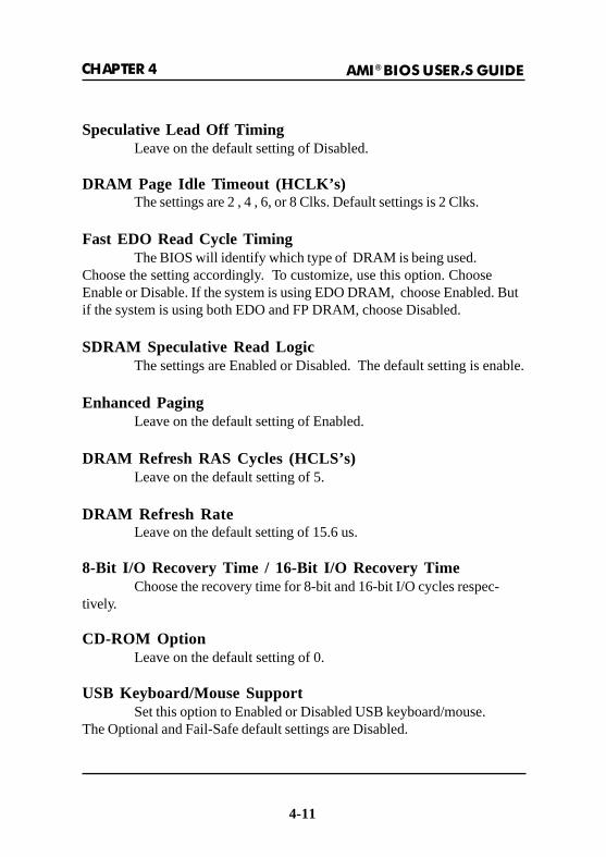
Speculative Lead Off TimingLeave on the default setting of Disabled.
DRAM Page Idle Timeout (HCLK’s)The settings are 2 , 4 , 6, or 8 Clks. Default settings is 2 Clks.
Fast EDO Read Cycle TimingThe BIOS will identify which type of DRAM is being used.
Choose the setting accordingly. To customize, use this option. ChooseEnable or Disable. If the system is using EDO DRAM, choose Enabled. Butif the system is using both EDO and FP DRAM, choose Disabled.
SDRAM Speculative Read LogicThe settings are Enabled or Disabled. The default setting is enable.
Enhanced PagingLeave on the default setting of Enabled.
DRAM Refresh RAS Cycles (HCLS’s)Leave on the default setting of 5.
DRAM Refresh RateLeave on the default setting of 15.6 us.
8-Bit I/O Recovery Time / 16-Bit I/O Recovery TimeChoose the recovery time for 8-bit and 16-bit I/O cycles respec-
tively.
CD-ROM OptionLeave on the default setting of 0.
USB Keyboard/Mouse SupportSet this option to Enabled or Disabled USB keyboard/mouse.
The Optional and Fail-Safe default settings are Disabled.

CHAPTER 4 AMI® BIOS USER�S GUIDE
4.5 Power Management Setup
1. Press <ENTER> on “Power Management Setup” of the main menuscreen.
2. Use <UP> and <DOWN> to choose the item and <PGUP> and<PGDN> keys to modify the highlighted item.
3. After you have finished with the Power Management Setup, press<ESC> to go back to the main menu.
AMIBIOS SETUP - POWER MANAGEMENT SETUP(C) 1996 American Megatrends, Inc. All Rights Reserved
Power Management / APM EnabledInstant On Support DisabledGreen PC Monitor Power State Stand ByVideo Power Down Mode SuspendHard Disk Power Down Mode Stand ByHard Disk Time Out (Minute) DisabledStandby Time Out (Minute) 10Suspend Time Out (Minute) 10Slow Clock Ratio 37.5-50%Display Activity IgnoreSerial port 1 MonitorSerial port 2 MonitorParallel port IgnoreFloppy disk IgnorePrimary IDE 0 MonitorPrimary IDE 1 MonitorSecondary IDE 0 IgnoreSecondary IDE 1 IgnoreResume on Ring DisabledModem Use IO Port N/AModem Use IRQ N/ASoft-Off by PWR-BTTN Instant-offRTC Alarm Resume From Soft Off DisabledRTC Alarm Date N/A
Available Options:EnabledDisabled
ESC:Exit :SelPgUp/PgDn:ModifyF2/F3:Color
4-12
RTC Alarm Hour N/ARTC Alarm Minute N/ARTC Alarm Second N/A

CHAPTER 4 AMI® BIOS USER�S GUIDE
Description of the item on screen follows:
Power Management/APMSet this option to Enabled to enable the Intel® 82371AB ISA power
management features and APM(Advanced Power Management). Thesettings are Enabled, Inst-On(instant-on) or Disabled. The Optimal and Fail-Safe default settings are Disabled.
Instant On Support (leave on the default setting of Disabled)
Green PC Monitor Power StateThis option specifies the power state that the green PC-compliant
video monitor enters when AMI® BIOS places it in a power savings stateafter the specified period of display inactivity has expired. The settings areOff, Standby, Suspend or Disabled. The Optimal and Fail-Safe defaultsettings are Standby.
Video Power Down ModeThis option specifies the power conserving state that the VESA
VGA video subsystem enters after the specified period of display inactivityhas expired. The settings are Disabled, Standby or Suspend. The Optimaland Fail-Safe default settings are Standby.
Hard Disk Power Down ModeThis option specifies the power conserving state that the hard disk
drive enters after the specified period of hard drive inactivity has expired.The settings are Disabled, Standby or Suspend. The Optimal and Fail-Safedefault settings are Disabled.
Hard Disk Timeout (Minute)This option specifies the length of a period of hard disk drive
inactivity. When this length of time expires, the computer enters power-conserving state specified in the Hard Disk Power Down mode option (seethe previous page). The settings are Disabled, 1 min, 2 min, 3 min, 4 min, 5min, 6 min, 7 min, 8 min, 9 min, 10 min, 11 min, 12 min, 13 min, 14 min or 15min. The Optimal and Fail-Safe default settings are Disabled.
4-13

CHAPTER 4 AMI® BIOS USER�S GUIDE
Standby Timeout (Minute)This option specifies the length of a period of system inactivity
while in Full power on state. When this length of time expires, the computerenters Standby power state. The settings are Disabled, 1 min, 2 min, 3 min, 4min, 5 min, 6 min, 7 min, 8 min, 9 min, 10 min, 11 min, 12 min, 13 min, 14 min or15 min. The Optimal and Fail-Safe default settings are Disabled.
Suspend Timeout (Minute)This option specifies the length of a period of system inactivity
while in Standby state. When this length of time expires, the computerenters Suspend power state. The settings are Disabled, 1 min, 2 min, 3 min, 4min, 5 min, 6 min, 7 min, 8 min, 9 min, 10 min, 11 min, 12 min, 13 min, 14 min or15 min. The Optimal and Fail-Safe default settings are Disabled.
Slow Clock RatioThis option specifies the speed at which the system clock runs in
power saving states. The settings are expressed as a ratio between thenormal CPU clock speed and the CPU clock speed when the computer is inthe power-conserving state. The settings are 1:1, 1:2, 1:4, 1:8, 1:16, 1:32, 1:64or 1:128. The Optimal and Fail-Safe defaults are 1:8.
Display Activity/Serial port 1/Serial port 2/Parallel port/Floppydisk/Primary IDE 0/Primary IDE 1/Secondary IDE 0/Secondary IDE 1
When set to Monitor, these options enable event monitoring on thespecified hardware interrupt request line. If set to Monitor and the computeris in a power saving state, AMI® BIOS watches for activity on the specifiedIRQ line. The computer enters the full on power state if any activity occurs.
AMI ® BIOS reloads the Standby and Suspend timeout timers ifactivity occurs on the specified IRQ line.
The settings for each of these options are Monitor or Ignore. TheOptimal and Fail-Safe default settings are Disabled for all the above optionsexcept IRQ3, IRQ4, IRQ7, IRQ12, IRQ14 or IRQ15. The Optimal defaultsettings for these options is Monitor.
4-14
CHAPTER 4 AMI® BIOS USER�S GUIDE
4-15
Resume on RingThis function is ring wake up system, from system OFF to ON.
During Disabled, the system will not turn on from modem ring wake up. Andduring Enabled, the system will boot up if there’s an incoming call from themodem.
Modem Use IO PortLeave on default setting of N/A.
Modem Use IRQThis indicates which IRQ no. will be used by the MODEM (if there
is a MODEM). The settings are 3, 4, 5 ,7 ,9, 10, or N/A.
Soft-Off by PWR-BTTNThe settings are Delay 4 sec or Instant-off. During Delay 4 sec, if
you push the switch one time the system goes into suspend mode and ifyou push it more than 4 second, the system will turn off. And duringInstant-off, the system will shut down once you push the switch.
RTC Alarm Resume From Soft OffThis function is for setting Date, Hour, Minute , and Second for
your system to boot up. During Disabled, you can not use this function.And during Enabled, Choose the Date, Hour, Minute, and Second:
RTC Alarm Date You can choose the date that the system willboot up.
RTC Alarm Hour You can choose the hour of the day that thesystem will boot up
RTC Alarm Minute You can choose the minute that the system willboot up.
RTC Alarm Second You can choose the second that the system willboot up.

CHAPTER 4 AMI® BIOS USER�S GUIDE
4.6 PCI/Plug and Play Setup
1. Press <ENTER> on “PCI/Plug and Play Setup” of the main menuscreen.
2. Use <UP> and <DOWN> to choose the item and <PGUP> and<PGDN> keys to modify the highlighted item.
3. After you have finished with the PCI/Plug and Play Setup, press<ESC> to go back to the main menu.
AMIBIOS SETUP - PCI/PLUG AND PLAY SETUP(C) 1996 American Megatrends, Inc. All Rights Reserved
Plug and Play Aware O/S NoReset NVRAM NoPCI Latency Timer (PCI Clocks) 64PCI VGA Palette Snoop DisabledPCI IDE Busmaster DisabledOffBoard PCI IDE Card AutoOffBoard PCI IDE Primary IRQ DisabledOffBoard PCI IDE Secondary IRQ DisabledAssign IRQ to PCI VGA YesPCI Slot1 IRQ Priority AutoPCI Slot2 IRQ Priority AutoPCI Slot3 IRQ Priority AutoPCI Slot4 IRQ Priority AutoDMA Channel 0 PnPDMA Channel 1 PnPDMA Channel 3 PnPDMA Channel 5 PnPDMA Channel 6 PnPDMA Channel 7 PnPIRQ3 ISAIRQ4 ISAIRQ5 PCI/PnPIRQ7 ISAIRQ9 PCI/PnP
Available Options:EnabledDisabled
ESC:Exit :SelPgUp/PgDn:ModifyF2/F3:Color
4-16
IRQ10 PCI/PnPIRQ11 PCI/PnPIRQ14 PCI/PnPIRQ15 PCI/PnPReserved Memory Size DisabledReserved Memory Address C8000
CHAPTER 4 AMI® BIOS USER�S GUIDE
Description of the item on screen follows:
Plug and Play Aware O/SSet this option to Yes if the operating system in this computer is
aware of and follows the Plug and Play specification. Currently, onlyWindows® 95 is PnP-aware. The settings are Yes or No. The Optimal andFail-Safe default settings No.
Clear NVRAMDuring Enabled, this option will clear the NVRAM on every boot.
PCI Latency Timer (PCI Clocks)This option specifies the latency timings (in PCI clocks) for all PCI
devices on the PCI bus. The settings are 32, 64, 96, 128, 160, 192, 224 or 248.The Optimal and Fail-Safe default settings are 64.
PCI VGA Palette SnoopWhen this option is set to Enabled, multiple VGA devices operating
on different buses can handle data from the CPU on each set of paletteregisters on every video device. Bit 5 of the command register in the PCIdevice configuration space is the VGA Palette Snoop bit (0 is disabled). Forexample, if there are two VGA devices in the computer (one PCI and ISA)and the Bit settings are:
Disabled - Data read and written by the CPU is only dircted to thePCI VGA device’s palette registers.
Enabled - Data read and written by the CPU is directed to theboth the PCI VGA device’s palette registers and theISA VGA device palette registers, permitting thepalette registers of both devices to be identical.
This option must be set to Enabled if an ISA adapter card requiresVGA palette snooping. The settings are Enabled or Disabled. The Optimaland Fail-Safe default settings are Disabled.
4-17

CHAPTER 4 AMI® BIOS USER�S GUIDE
PCI IDE BusMasterSet this option to Enabled to specify that the IDE controller on the
PCI local bus includes a bus mastering capability. The settings are Enabledor Disabled. The Optimal and Fail-Safe default settings are Disabled.
Offboard PCI IDE CardThis option specifies if an offboard PCI IDE controller adapter card
is installed in the computer. You must specify the PCI expansion slot on themainboard where the offboard PCI IDE controller is installed. If an offboardPCI IDE controller is used, the onboard IDE controller is automaticallydisabled. The settings are Auto (AMI® BIOS automatically determineswhere the offboard PCI IDE controller adaper card is installed), Slot1, Slot2,Slot3 or Slot4. The Optimal and Fail-Safe settings are Auto.
If an offboard PCI IDE controller adapter card is installed in thecomputer, you must also set the Offboard PCI IDE Primary IRQ and OffboardPCI IDE Secondary IRQ options.
Offboard PCI IDE Primary IRQ/Offboard PCI IDE Secondary IRQ
These options specify the PCI interrupt used by the Primary (orSecondary) IDE channel on the offboard PCI IDE controller. The settings areDisabled, Hardwired, INTA, INTB, INTC or INTD. The Optimal and Fail-Safedefault settings are Disabled.
Assign IRQ to PCI VGAChoose the IRQ to be assigned to the PCI VGA display adapter card.
The Optimal and Fail-Safe default settings No.
4-18

CHAPTER 4 AMI® BIOS USER�S GUIDE
DMA Channel 0/DMA Channel 1/DMA Channel 3/DMAChannel 5/DMA Channel 6/DMA Channel 7
These options specify the bus that the specified DMA channel isused. These options allow you to reserve DMAs for legacy ISA adaptercards.
These options determine if AMI® BIOS should remove a DMA fromthe available DMAs passed to devices that are configurable by the systemBIOS. The available DMA pool is determined by reading the ESCDNVRAM. If more DMAs must be removed from the pool, the end user canuse these options to reserve the DMA by assigning an ISA/EISA setting toit.
IRQ3/IRQ4/IRQ5/RQ7/IRQ9/IRQ10/IRQ11/IRQ14/IRQ15These options specify the bus that the specified IRQ line is used
on. These options allow you to reserve IRQs for legacy ISA adapter cards.These options determine if AMI® BIOS should remove an IRQ from
the pool of available IRQs passed to devices that are configurable by thesystem BIOS. The available IRQ pool is determined by reading the ESCDNVRAM. If more IRQs must be removed from the pool, the end user can usethese options to reserve the IRQ by assigning an ISA/EISA setting to it.Onboard I/O is configured by AMI® BIOS. All IRQs used by onboard I/Oare configured as PCI/PnP. If all IRQs are set to ISA/EISA and IRQ14 and 15are allocated to the onboard PCI IDE, IRQ9 will still be available for PCI andPnP devices, because at least one IRQ must be available for PCI and PnPdevices. The settings are ISA/EISA or PCI/PnP. The Optimal and Fail-Safedefault settings are IRQ3 through 7 are ISA/EISA. The Optimal and Fail-Safedefault settings PCI/PnP.
4-19

CHAPTER 4 AMI® BIOS USER�S GUIDE
Reserved Memory SizeThis option specifies the size of the memory area reserved for
legacy ISA adapter cards. The settings are Disabled, 16K, 32K, or 64K.The Optimal and Fail-Safe default settings are Disabled.
Reserved Memory AddressThis option specifies the beginning address (in hex) of the
reserved memory area. The specified ROM memory area is reserved foruse by legacy ISA adapter cards.
4-20

CHAPTER 4 AMI® BIOS USER�S GUIDE
4.7 Peripheral Setup
1. Press <ENTER> on “Peripheral Setup” of the main menu screen.
2. Use <up> and <down> to choose the item and <PgUp> and<PgDn> keys to modify the highlighted item.
3. After you have finished with the Peripheral Setup, press <ESC> togo back to the main menu.
AMIBIOS SETUP - PERIPHERAL SETUP(C) 1996 American Megatrends, Inc. All Rights Reserved
OnBoard FDC EnabledOnBoard Serial PortA 3F8h/COM1OnBoard Serial PortB 2F8h/COM2IR Port Support Disabled IR Base Address Select 2E8 IR IRQ Select 10OnBoard Parallel Port 378 Parallel Port Mode Normal EPP Version N/A Parallel Port IRQ 7 Parallel Port DMA Channel N/AOnboard IDE Both
Available Options:EnabledDisabled
ESC:Exit :SelPgUp/PgDn:ModifyF2/F3:Color
4-21

CHAPTER 4 AMI® BIOS USER�S GUIDE
Description of the item on screen follows:
Onboard FDCChoose Auto, for the BIOS to automatically detect the device
Choose Enabled, Enabling onboard FDC.Choose Disabled, Disabling onboard FDC.The Optimal and Fail-Safe default settings are Auto.
Onboard Serial Port A/Onboard Serial Port BChoose Enabled, for the BIOS to automatically detect the device.
If the ISA add-on card has Onboard FDC to be set at
FDC exist
none FDC exist
Disabled
Enabled
ü ü ü ü DISABLED X DISABLED X
ü ü X X COM3 4 COM4 3
X X ü ü COM1 4 COM2 3
ü X X ü COM2 3 COM3 4
X ü ü X COM1 4 COM4 3
ü ü ü X COM4 3 DISABLED X
ü ü X ü COM3 4 DISABLED X
ü X ü ü COM2 3 DISABLED X
X ü ü ü COM1 4 DISABLED X
X X X X COM1 4 COM2 3
ü X X X COM2 3 COM3 4
X ü X X COM1 4 COM3 4
X X ü X COM1 4 COM2 3
X X X ü COM1 4 COM2 3
If the ISA add-on card has Onboard Serial port to be set at
COM1(I/O:3F8H)
COM2(I/O:3F8H)
COM3(I/O:3E8H)
COM4(I/O:2E8H)
PORT1 PORT2IRQ
ASSIGNEDIRQ
ASSIGNED
Note: If the onboard serial port interrupt and ISA add-on cardinterrupt are in conflict, the serial port will not work properly. Pleasedisable one of the devices.
4-22

CHAPTER 4 AMI® BIOS USER�S GUIDE
IR Port Support (leave on the default setting of Disabled)
Onboard Parallel PortChoose Auto, for the BIOS to automatically assigned onboard
parallel port to available parallel port or disabled
If the ISA add-on card has Onboard parallel port
ü ü ü Disabled X
ü ü X LPT3 5
ü X ü LPT2 5
X ü ü LPT1 7
ü X X LPT2 5
X ü X LPT1 7
X X ü LPT1 7
X X X LPT1 7
LPT1I/O:378H
LPT2I/O:278H
LPT3I/O:3BCH
PORTASSIGNED
IRQASSIGNED
Note: If the onboard parallel port interrupt and ISA add-on card interrupt arein conflict, the parallel port will not work properly. Please disable one ofthe devices.
4-23
Parallel Port ModeThis option allows user to choose the operating mode of the
onbaord parallel port. The settings are Normal, SPP/EPP or ECP mode.
EPP Version(leave on the default setting of N/A)

CHAPTER 4 AMI® BIOS USER�S GUIDE
Parallel Port IRQIf the onboard parallel mode is not on auto mode, the user can
select the interrupt line for onboard parallel port. We suggest that the userselect the interrupt for the onboard parallel port as shown below:
Parallel Port DMA ChannelThis option allows user to choose DMA channel 1 to 3 for the
onboard parallel port on ECP mode.
Onboard IDESet this option to enable or disable on board IDE controller.
Onboard parallel port set at Parallel Port IRQ
LPT1(378H)
LPT2(278H)
LPT3(3BCH)
7
5
5
4-24

CHAPTER 4 AMI® BIOS USER�S GUIDE
4.8 Hardware Monitor Setup
This settings are use by LM78 chipset which is an optionalfunction. To enable the best performance, leave all the setting on thedefault mode.
AMIBIOS SETUP - PERIPHERAL SETUP(C) 1996 American Megatrends, Inc. All Rights Reserved
CPU Type PentiumCPU Current Voltage (V) 3.3
--- LM78 Setup ---CPU Thermal Setup ( oC) 60CPU Current Temperature ( oC) 30Thermal Slow Clock Ratio 75%CPU Temperature Display yesSystem Temperature Set ( oC) 50System Current Temperature ( oC) 29Chassis Intrusion DisabledPower FAN Message Display NoCPU FAN Message Display YesSystem Temperature Display Yes
Available Options:
ESC:Exit :SelPgUp/PgDn:ModifyF2/F3:Color
4-25

CHAPTER 4 AMI® BIOS USER�S GUIDE
Description of the item on screen follows:
CPU Thermal SetupThis is for setting the CPU temperature. You must leave this on the
default setting of 60.
CPU Current TemperatureThis will show the CPU Current temperature.
Thermal Slow Clock RatioThis will show the thermal slow clock ratio
CPU Temperature DisplayIf set to yes, during boot-up this will show the CPU temperature.
System Temperature SetThis is for setting the system temperature. You must leave this on
the default setting of 50.
System Current TemperatureThis wil show the current temperaure of the system.
Chassis IntrusionDuring Enabled, the on-board chassis intrusion sensor will monitor
any intrusion on the chassis.
Power FAN Message Display/CPU FAN Message DisplayIf set to yes, if any of the fan malfunction then it will show warning
messages.
System Temperature DisplayIf set to yes, if the temperature gets to high or to low, this will show
warning messages.
4-26