Chap 4. Sequential Circuits. Sequential Circuit Definitions sequential circuit –combinational...
20
Chap 4. Sequential Circuits Chap 4. Sequential Circuits
-
Upload
johnathan-thomas -
Category
Documents
-
view
259 -
download
0
Transcript of Chap 4. Sequential Circuits. Sequential Circuit Definitions sequential circuit –combinational...

Chap 4. Sequential CircuitsChap 4. Sequential Circuits

Sequential Circuit DefinitionsSequential Circuit Definitions sequential circuit
– combinational circuit + storage elements– storage elements
• store binary information state of the sequential circuit at given state
– outputs are a function of the inputs & present state of the storage elements
– next state of storage elements is also a function of the inputs & the present state

Sequential Circuit DefinitionsSequential Circuit Definitions
flip-flop– storage elements employed in clocked sequential circuits– a binary storage device capable of storing one bit of info– Normally, a sequential circuit uses many flip-flops – the transition from one state to the other occurs only at
predetermined time intervals dictated by the clock pulses– two outputs: normal & complemented values
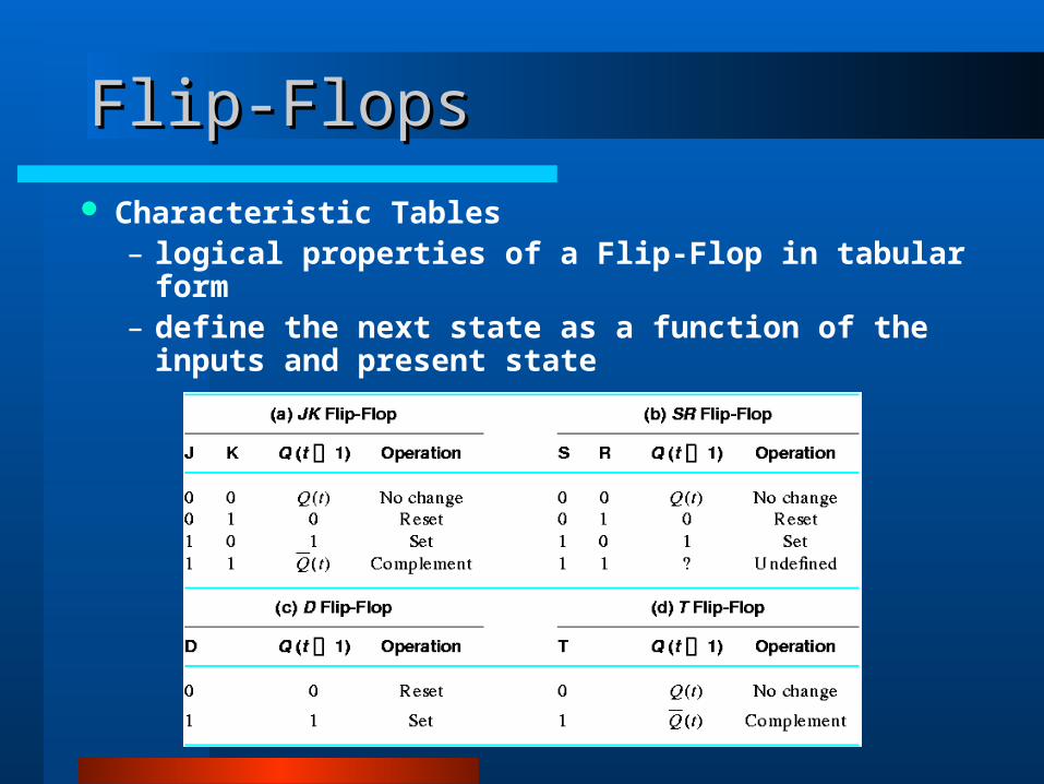
Flip-FlopsFlip-Flops
Characteristic Tables– logical properties of a Flip-Flop in tabular form– define the next state as a function of the inputs and
present state

Sequential Circuit Analysis
behavior of a sequential circuit– is determined from inputs, outputs, & present
state of the circuit– outputs & the next state are function of inputs
& present state
Input Equations– a logic diagram of sequential circuit includes
F-Fs (any type), or combinational circuit– the part of the combinational circuit can be
described by a set of Boolean functions, called input equations

Sequential Circuit Analysis
(ex) JA = XB + Y'C, KA = YB' + C- J & K are the inputs of a JK F/F
- A is the name of the F/F output
• F/F input equations constitute a convenient algebraic expressions for specifying the logic diagram of a sequential circuit

Sequential Circuit Analysis
(ex) DA = AX + BX, DB = A'X, Y = (A+B) X'
(input equations for F-F) (eqs for output Y)

Sequential Circuit Analysis
State Table– functional relationship between inputs, outputs, & flip-flop
state
– consist of 4 sections: present state, input, next state, output• list all possible combinations of present state and inputs• next state shows states of F-F one clock period later at time t+1
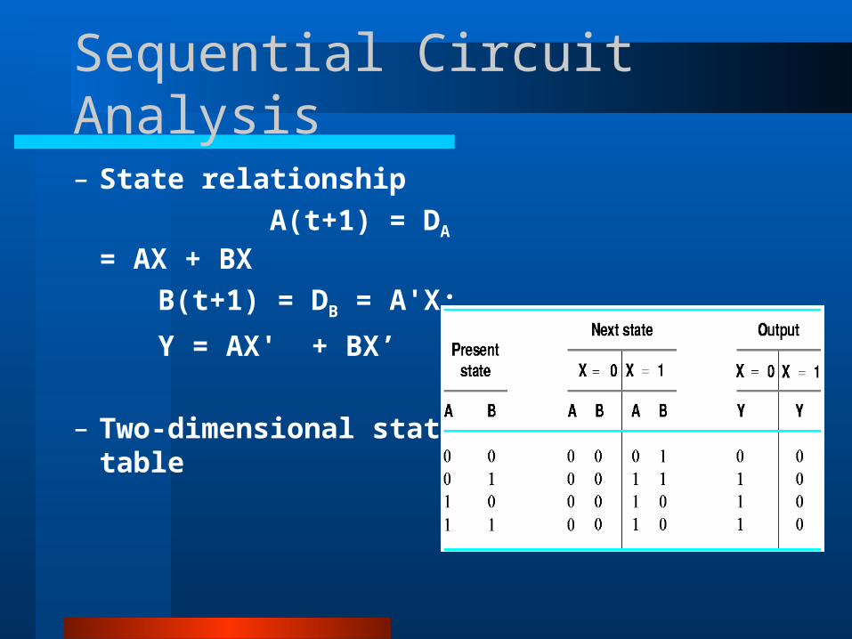
Sequential Circuit Analysis
– State relationship
A(t+1) = DA = AX + BX
B(t+1) = DB = A'X;
Y = AX' + BX’
– Two-dimensional state table

Sequential Circuit Analysis
Analysis with JK Flip-flops– next state values are obtained by a 2 step procedure:
1) Obtain the binary values of each F/F input equation
in terms of the present state & input variables
2) Use the corresponding F/F characteristic (Table 4.1)
to determine the next state
(Ex) A sequential circuit with 2 JK F/F
JA = B, KA = B'X
JB = X', KB = AX' + A'X

Sequential Circuit Analysis- state diagram
binary number inside circle = state of F-F directed lines are labeled with (input/output) value

Sequential Circuit DesignSequential Circuit Design
– Combinational circuit: fully specified by a truth table– Sequential circuit requires a state table for its specification
• first step is to obtain a state table (or state diagram)
– Number of F/F is determined from the number of states (up to 2n)
Design Procedure with D F/Fs 1) Obtain the state diagram
(from problem statement, or state diagram) 2) Obtain the state table 3) Assign binary codes to the states 4) Derive F-F input eqs from next state conditions in table 5) Derive the output functions if needed 6) Simplify the input equations & output functions 7) Draw the logic diagram with D F-Fs & combinational gates
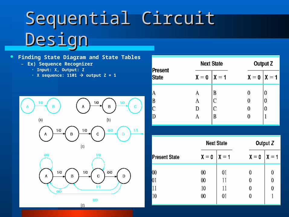
Sequential Circuit DesignSequential Circuit Design Finding State Diagram and State Tables
– Ex) Sequence Recognizer• Input: X, Output: Z• X sequence: 1101 output Z = 1

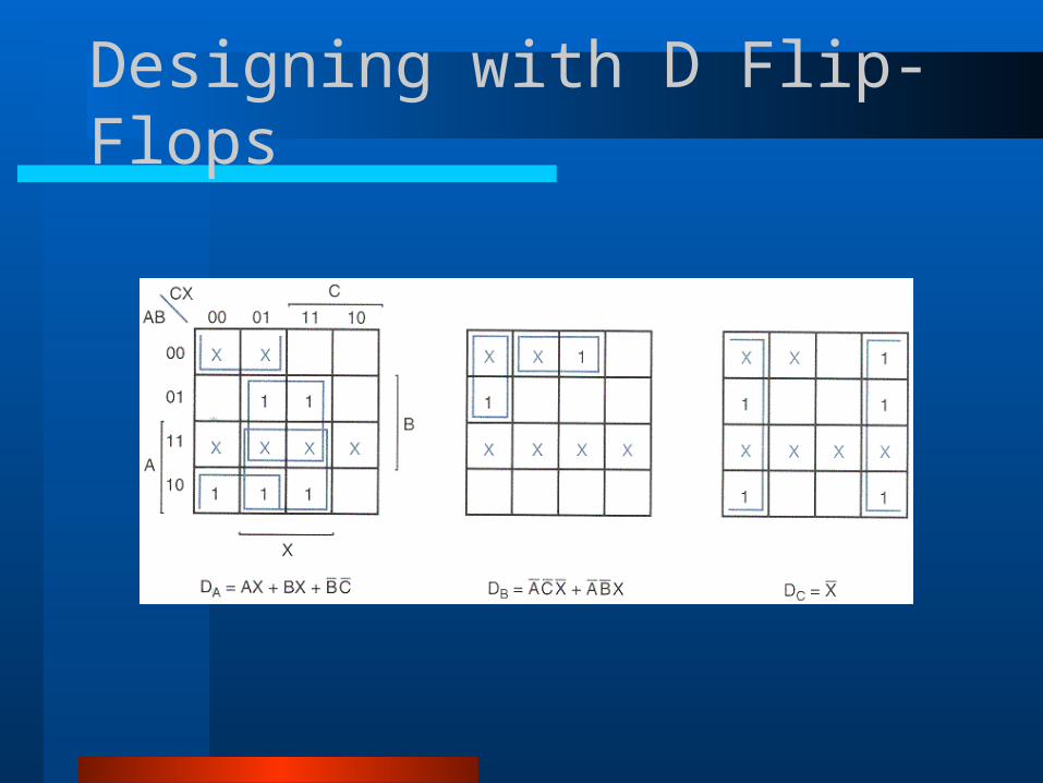
Designing with D Flip-Flops
A(t+1) = DA(A,B,X) = m(2,4,5,6)
B(t+1) = DB(A,B,X) = m(1,3,5,6)
Y(A,B,X) = m(1,5)
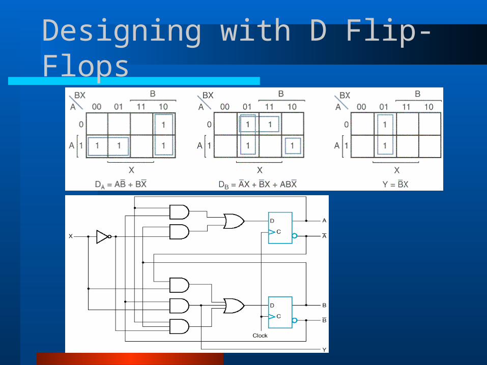
Designing with D Flip-Flops
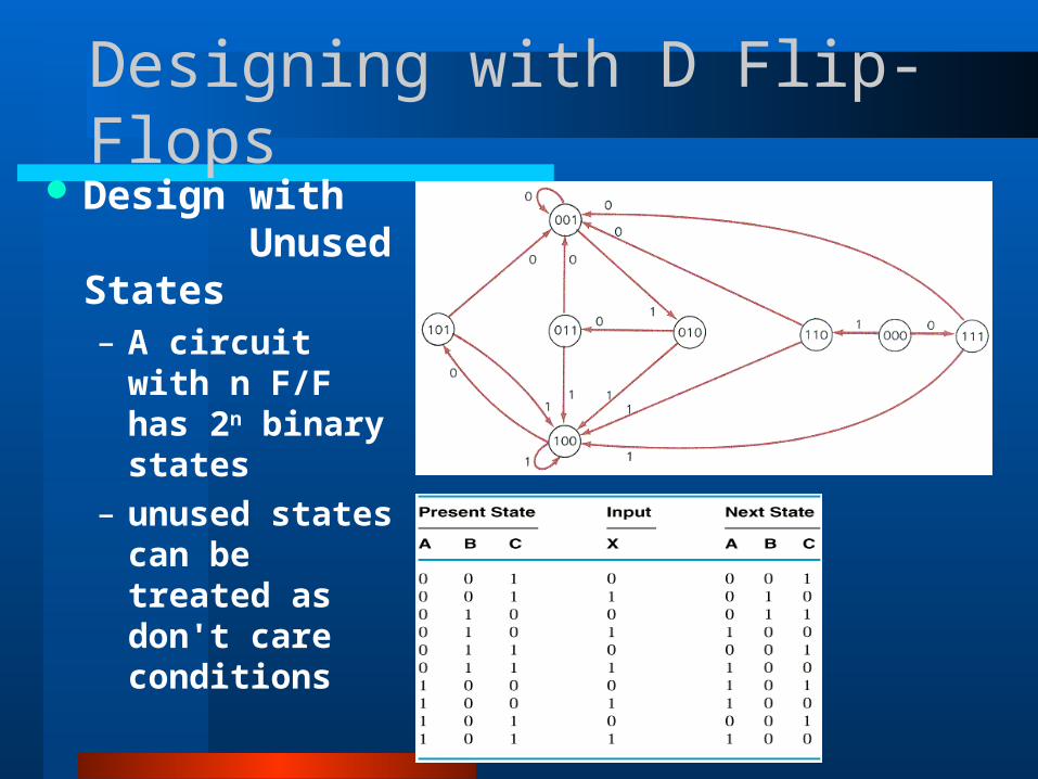
Designing with D Flip-Flops Design with
Unused States– A circuit with n
F/F has 2n binary states
– unused states can be treated as don't care conditions
Designing with D Flip-Flops

Design with JK Flip-flops
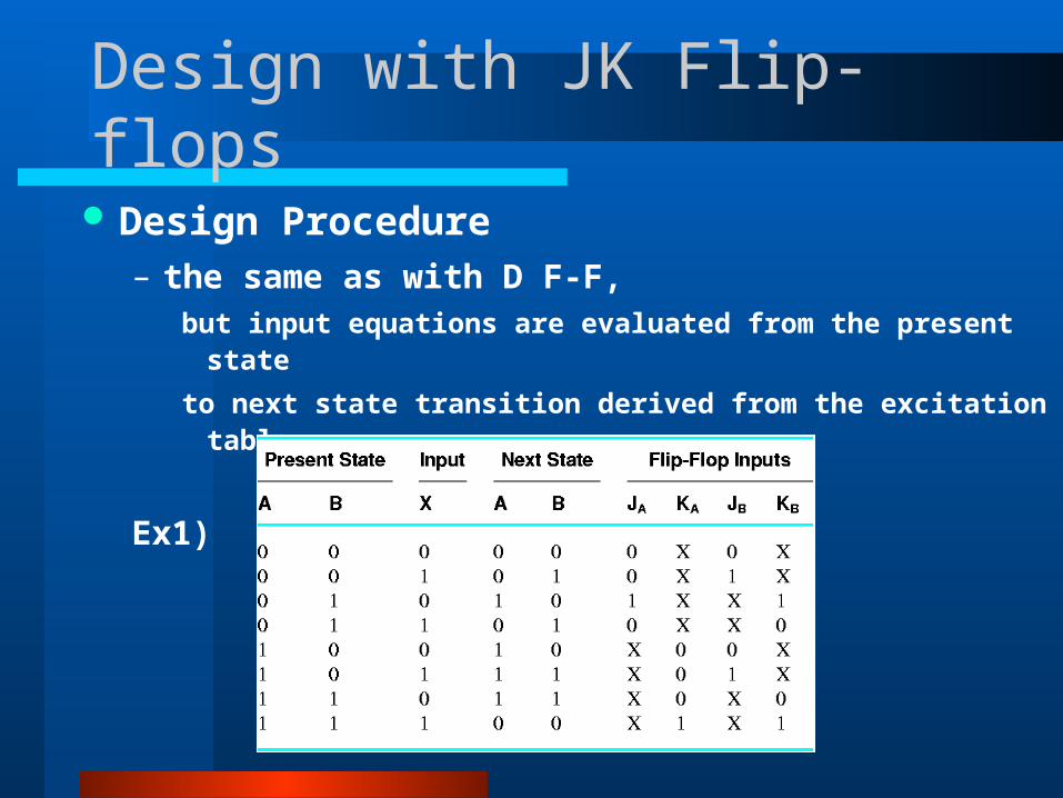
Design with JK Flip-flops
Design Procedure– the same as with D F-F,
but input equations are evaluated from the present state
to next state transition derived from the excitation table
Ex1)

Design with JK Flip-flops
• specify the truth table for input equations as a function of present state A, B & X• simplify using k-map