Chalcogenide electronic materials research: … CSRA - Lany... · First principles calculations of...
47
First principles calculations of electronic structure, defects, disorder Stephan Lany, National Renewable Energy Laboratory, Golden, CO Thin film growth Rafael Jaramillo, Massachusetts Institute of Technology, Cambridge, MA High-throughput computation and thermoelectrics Prashun Gorai, Colorado School of Mines and NREL, Golden, CO Thin film characterization Rafael Jaramillo Symposium F.1 Chalcogenide Semiconductor Research and Applications Tutorial Chalcogenide electronic materials research: Computation, synthesis, characterization
Transcript of Chalcogenide electronic materials research: … CSRA - Lany... · First principles calculations of...
First principles calculations of electronic structure, defects, disorder
Stephan Lany, National Renewable Energy Laboratory, Golden, CO
Thin film growth Rafael Jaramillo, Massachusetts Institute of Technology, Cambridge, MA
High-throughput computation and thermoelectrics Prashun Gorai, Colorado School of Mines and NREL, Golden, CO
Thin film characterization
Rafael Jaramillo
Symposium F.1 Chalcogenide Semiconductor Research and Applications Tutorial
Chalcogenide electronic materials research: Computation, synthesis, characterization
First principles calculations: Electronic structure, defects, disorder
Stephan Lany
National Renewable Energy Laboratory,
Golden, CO
Tutorial

What do we want to predict by theory?
Properties of semiconductors
• Structure (total-energy)
Inter-atomic potentials (Lennard-Jones, Morse, VFF)
Electrostatic interactions
Quantum-mechanical (DFT)
• Thermodynamic stability (total-energy)
Quantum-mechanical (DFT)
• Defects and doping (total-energy)
Cavity model for vacancies
Model potentials (e.g., Morse)
Quantum-mechanical (DFT)
• Band-structure (quasi-particle energies)
Empirical (tight-binding, k∙p, EPM, NLEP)
Quantum-mechanical (Hartree-Fock CI, CC, MCSCF)
Quantum-mechanical (DFT GW)

Working horse of electronic structure theory:
Local Density Approximation (LDA)
Schrödinger’s equation:
General Quantum mechanics:
Density Functional Theory: SVe includes self-interaction
VXC corrects for SI,
many-particle effects
Hohenberg-Kohn 1964, applications ~70s, Perdew–Zunger LDA 1981
• High accuracy for electronic density and total-energies
• Usually not sufficiently accurate for single-particle energies

5
Electronic structure and optical properties

Empirical approaches
Empirical approaches for band structure calculation
Tight-binding (LCAO), k∙p, empirical pseudopotentials
(1) Fit parameters to reference data
(experiment, accurate theory)
(2) Assuming transferability,
apply to more complex cases
Full BZ, alloys, nanostructures, ...
Energy-band interpolation scheme based on a pseudopotential
J.C. Phillips, Phys. Rev. 112, 685 (1958)
Nonlocal pseudopotential calculations for the electronic structure
of eleven diamond and zinc-blende semiconductors
J.R. Chelikowsky, M.L. Cohen, Phys. Rev. B 14, 556 (1976)

7
Properties for energy materials: Band structure calculation
Band-structures and band gaps with DFT starting point
• Starting from DFT, calculate electron self energy Σ, get quasiparticle energy correction to DFT
GW approximation for self energy Σ
G: Green’s function, W: screened Coulomb interaction
• GW uses the screened Coulomb potential (cf. “screened exchange”) For main group compounds, GW
calculations give band gaps in very good agreement with experiment
M. van Schilfgaarde et al., PRL 96, 226402 (2006)
Importance of electronic-structure
• Band-gaps, band-structure, optical properties (α, ε), transport: effective masses
• Energy materials: Photovoltaics, solar fuels, thermoelectrics, electronic materials, battery materials

GW calculation of band-structure and optical properties
Implementation and performance of the frequency-dependent GW
method within the PAW framework, M. Shishkin, G. Kresse, Phys.
Rev. B 74, 035101 (2006)
Dielectric properties and excitons for extended systems from
hybrid functionals, J. Paier, M. Marsman, and G. Kresse, Phys. Rev.
B 78, 121201(R) (2008)
Many-body perturbation theory in GW
approximation implemented in numerous codes
(VASP, BerkeleyGW, Questaal, Yambo)
More demanding than DFT calculations:
- CPU and memory requirements
- Convergence, self-consistency, vertex-corrections
- 3d transition metals
Optical properties from dielectric function
e(w) + ie2(w)
- independent particle approximation
- Bethe-Salpeter equation (excitonic effects)
SnS
expt.
GW GW+exc.
J. Vidal et al., Appl. Phys. Lett. 100, 032104 (2012)
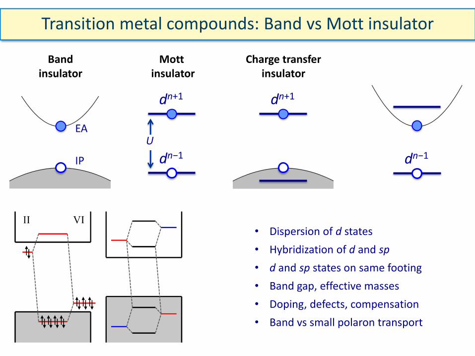
Transition metal compounds: Band vs Mott insulator
EA
Band insulator
IP
Mott insulator
dn+1
dn−1
Charge transfer insulator
dn+1
• Dispersion of d states
• Hybridization of d and sp
• d and sp states on same footing
• Band gap, effective masses
• Doping, defects, compensation
• Band vs small polaron transport
dn−1
U
10
d
GW(RPA) GW+Vd GGA+U
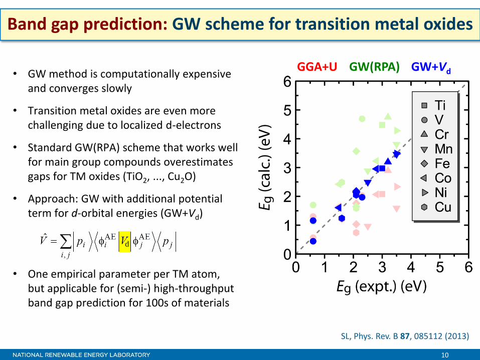
Band gap prediction: GW scheme for transition metal oxides
• GW method is computationally expensive and converges slowly
• Transition metal oxides are even more challenging due to localized d-electrons
• Standard GW(RPA) scheme that works well for main group compounds overestimates gaps for TM oxides (TiO2, ..., Cu2O)
• Approach: GW with additional potential term for d-orbital energies (GW+Vd)
• One empirical parameter per TM atom, but applicable for (semi-) high-throughput band gap prediction for 100s of materials
SL, Phys. Rev. B 87, 085112 (2013)
11
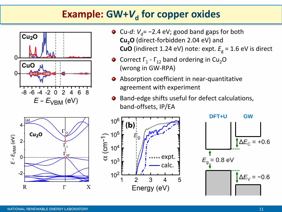
Example: GW+Vd for copper oxides
Cu-d: Vd= −2.4 eV; good band gaps for both Cu2O (direct-forbidden 2.04 eV) and CuO (indirect 1.24 eV) note: expt. Eg = 1.6 eV is direct
Correct Γ1 - Γ12 band ordering in Cu2O (wrong in GW-RPA)
Absorption coefficient in near-quantitative agreement with experiment
Band-edge shifts useful for defect calculations, band-offsets, IP/EA
Eg = 0.8 eV
ΔEV = −0.6
ΔEC = +0.6
DFT+U GW
expt. calc.
12
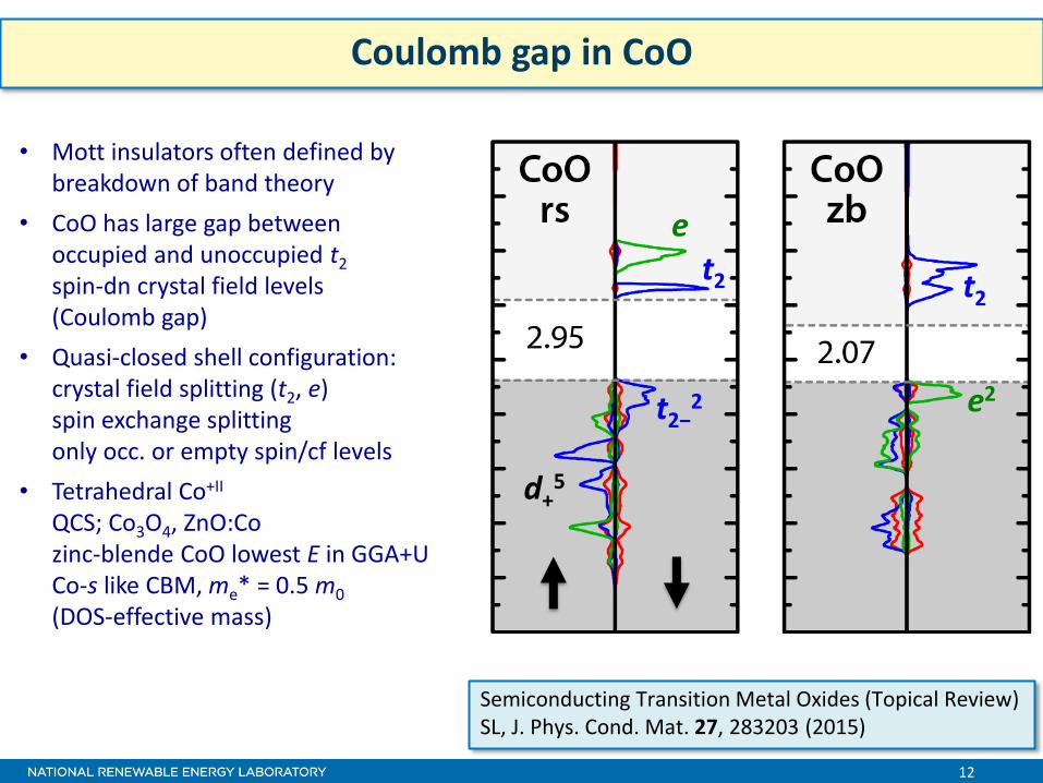
Coulomb gap in CoO
e
t2−2
• Mott insulators often defined by breakdown of band theory
• CoO has large gap between occupied and unoccupied t2 spin-dn crystal field levels (Coulomb gap)
• Quasi-closed shell configuration: crystal field splitting (t2, e) spin exchange splitting only occ. or empty spin/cf levels
• Tetrahedral Co+II QCS; Co3O4, ZnO:Co zinc-blende CoO lowest E in GGA+U Co-s like CBM, me* = 0.5 m0 (DOS-effective mass)
d+5
t2 t2 t2
e2
Semiconducting Transition Metal Oxides (Topical Review) SL, J. Phys. Cond. Mat. 27, 283203 (2015)
13
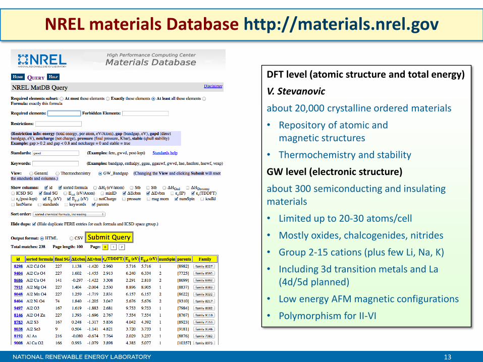
NREL materials Database http://materials.nrel.gov
DFT level (atomic structure and total energy)
V. Stevanovic
about 20,000 crystalline ordered materials
• Repository of atomic and magnetic structures
• Thermochemistry and stability
GW level (electronic structure)
about 300 semiconducting and insulating materials
• Limited up to 20-30 atoms/cell
• Mostly oxides, chalcogenides, nitrides
• Group 2-15 cations (plus few Li, Na, K)
• Including 3d transition metals and La (4d/5d planned)
• Low energy AFM magnetic configurations
• Polymorphism for II-VI
14
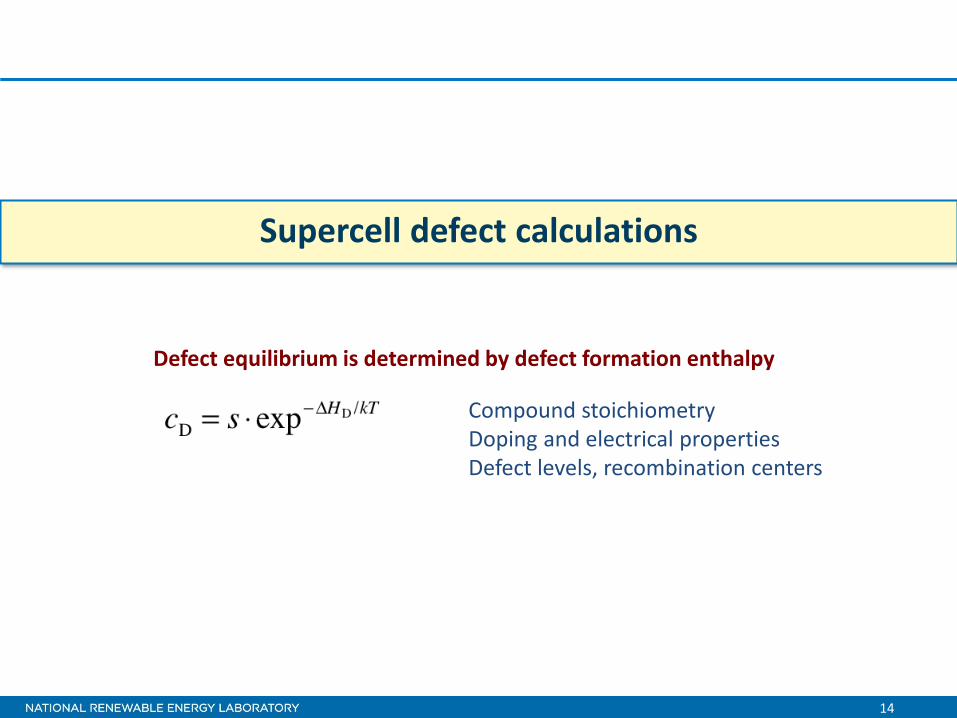
Supercell defect calculations
Defect equilibrium is determined by defect formation enthalpy
Compound stoichiometry Doping and electrical properties Defect levels, recombination centers

15
Defect formation energy
ΔμX ΔEF ΔμA = 0 (A metal)
ΔμX = 0 (elem. X)
CBM VBM
supercell energies electron reservoir atomic reservoir

Supercell corrections vs. finite-size scaling
DH(L)=DH()
DH(L)=DH() + g1/L + g3/L3
DH(L)=DH() + g1/L
Finite-size scaling
Form
ation e
nerg
y D
H [
eV
]
Conclusions
• image charge + pot. alignment
correction give accurate DH
• Avoid FCC symmetries!
• Simple but accurate corrections
available
FCC
S. Lany, A. Zunger, Phys. Rev. B 78, 235104 (2008); Modelling Simul. Mater. Sci. Eng. 17 084002 (2009)
C. Freysoldt, J. Neugebauer, C.G. van de Walle, Phys. Rev. Lett. 102, 016402 (2009)
17
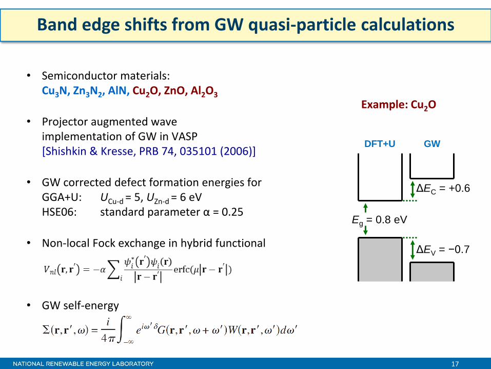
Band edge shifts from GW quasi-particle calculations
• Semiconductor materials: Cu3N, Zn3N2, AlN, Cu2O, ZnO, Al2O3
• Projector augmented wave implementation of GW in VASP [Shishkin & Kresse, PRB 74, 035101 (2006)]
• GW corrected defect formation energies for GGA+U: UCu-d = 5, UZn-d = 6 eV HSE06: standard parameter α = 0.25
• Non-local Fock exchange in hybrid functional
• GW self-energy
Eg = 0.8 eV
ΔEV = −0.7
ΔEC = +0.6
DFT+U GW
Example: Cu2O

18
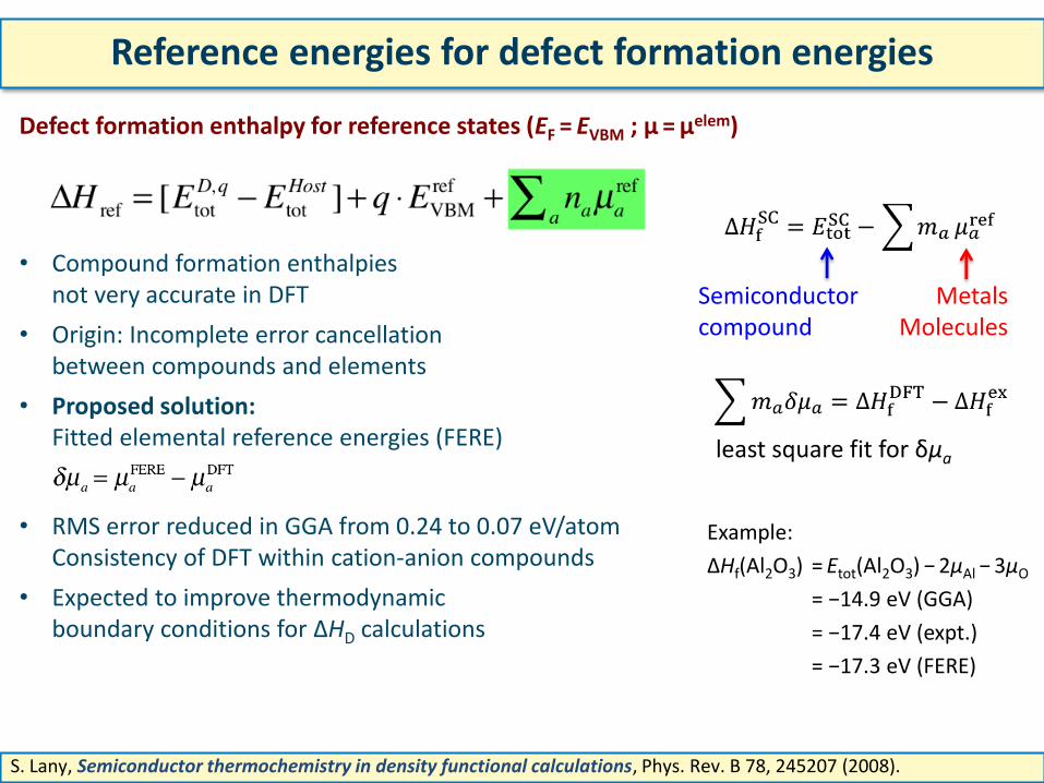
Reference energies for defect formation energies
H. Peng, D.O. Scanlon, V. Stevanovic, J. Vidal, G.W. Watson, S. Lany, Convergence of density and hybrid functional defect calculations for compound semiconductors, Phys. Rev. B 88, 115201 (2013).
Defect formation enthalpy for reference states (EF = EVBM ; μ = μelem)
• “Band gap problem of DFT” affects EVBM
• Proposed solution: Anchor ΔHD at the average potential, use band edge shifts from GW
• Compare standard DFT (GGA+U) with hybrid functional (HSE06) calculations
19
Reference energies for defect formation energies
Defect formation enthalpy for reference states (EF = EVBM ; μ = μelem)
• Compound formation enthalpies not very accurate in DFT
• Origin: Incomplete error cancellation between compounds and elements
• Proposed solution: Fitted elemental reference energies (FERE)
• RMS error reduced in GGA from 0.24 to 0.07 eV/atom Consistency of DFT within cation-anion compounds
• Expected to improve thermodynamic boundary conditions for ΔHD calculations
Semiconductor compound
Metals Molecules
least square fit for δμa
Example:
ΔHf(Al2O3) = Etot(Al2O3) − 2μAl − 3μO
= −14.9 eV (GGA)
= −17.4 eV (expt.)
= −17.3 eV (FERE)
S. Lany, Semiconductor thermochemistry in density functional calculations, Phys. Rev. B 78, 245207 (2008).

20
Comparison of density and hybrid functionals
FERE δμ PBE+U
eV HSE eV
Cu −0.02 ±0.00
Zn −0.08 +0.24
Al +0.66 +0.35
N −0.03 −0.04
O +0.34 +0.32
Eg
PBE+U eV
HSE eV
GW eV
Cu3N 0.8 1.0 1.0
Zn3N2 0.2 0.9 1.1
AlN 4.2 5.6 6.4
Cu2O 0.8 2.0 2.2
ZnO 1.5 2.5 3.5
Al2O3 6.3 8.1 9.9
ΔEVBM
PBE+U eV
HSE eV
Cu3N −0.4 −0.3
Zn3N2 −0.4 −0.1
AlN −1.3 −0.5
Cu2O −0.7 −0.4
ZnO −1.1 −0.6
Al2O3 −1.9 −0.7
H. Peng, D.O. Scanlon, V. Stevanovic, J. Vidal, G.W. Watson, S. Lany, Convergence of density and hybrid functional defect calculations for compound semiconductors, Phys. Rev. B 88, 115201 (2013).
Band gaps VBM energy Elemental energy
21
Defect equilibria and “defect phase diagrams”

Thermodynamic modeling
Temperature dependence of band gap (CBM)
Dopant-defect association / dissociation within law of mass action
K. Biswas and S. Lany, Phys. Rev. B 80, 115206 (2009)

23
Example: n-type doping in ZnO
Formation energies of dopants, defects and defect pairs 192 atoms supercells, GGA+U, ΔEV (GW), fitted elemental reference energies (FERE) [1]
Active players:
Isolated dopants/defects: GaZn1+, VZn
2−, VO0/2+
Pairs and complexes: (GaZn - VZn)1−
(2GaZn - VZn)0 Law of mass action
[(GaZn-VZn)] = [GaZn]×[VZn]×exp(−Eb1/kT)
[(2GaZn-VZn)] = [GaZn]2×[VZn]×exp(−Eb2/kT)
Ga Ga VZn
Eb1 = −1.1 eV
Eb2 = −1.8 eV

24
Solubility limit of Al, Ga, In in ZnO
Solubility in the per cent range only at high temperatures above 1000oC At equilibrium conditions, moderate compensation (up to ~10%)
pO2 = 1 atm pO2 = 10−8 atm
“Oxidizing” “Reducing”
Limiting competing oxide-phases: Al2ZnO4, Ga2ZnO4, In2O3
Equilibrium of ZnO: ΔμZn + ΔμO = ΔHf(ZnO)
dopant: 2ΔμAl + ΔμZn +4 ΔμO = ΔHf(Al2ZnO4)
InZn
GaZn
AlZn InZn
GaZn
AlZn In-metal

25
Influence of band edge shift and defect pairs
“2007” model
incl. GW band edge shifts increases n
incl. defect pair binding reduces n
Strong compensation at high (supersaturated) Ga dopant concentrations,
most compensating defects (VZn) occur as fully passivated complexes (2GaZn - VZn)
Constrained equilibrium: c(GaZn) is constant, but compensation by VZn is equilibrated
Large, counteracting effects

26
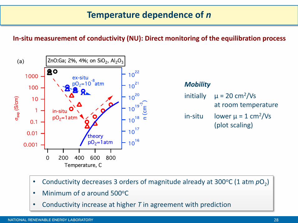
Temperature dependence of n
Why does n increase with T?
- reduction of ΔμO with T at given pO2 respective increase of ΔμZn and ΔHD(VZn)
- reduction of band gap (ECBM) ΔEg/ΔT = 0.6 meV/K
F.J. Manjon et al, Sol. Stat. Comm. 128, 35 (2003)
EVBM ECBM EFermi
DH
D
VZn2−
ΔEg
ΔμZn
1 atm
10−8 atm
Constrained equilibrium (2% cat. Ga)

27
Comparison with as-grown doped ZnO
Highly doped ZnO:Al, ZnO:Ga only as thin-films Typical literature growth methods and results • PLD, Sputtering, MOCVD • Tsub ≈ 200-300 oC • pO2 ≤ 10−6 atm • c(Al,Ga) up to 5% cat. • n ≈ 1021 cm−3
As-grown films have much higher dopant concentration than predicted equilibrium solubility limit (not so surprising) As-grown films have much higher carrier concentration than predicted for constrained equilibrium at moderate T (surprising?)
ZnO:Ga, PLD (pO2 = 10−8 atm)
28
Temperature dependence of n
Mobility
initially μ = 20 cm2/Vs at room temperature
in-situ lower μ = 1 cm2/Vs (plot scaling)
• Conductivity decreases 3 orders of magnitude already at 300oC (1 atm pO2)
• Minimum of σ around 500oC
• Conductivity increase at higher T in agreement with prediction
In-situ measurement of conductivity (NU): Direct monitoring of the equilibration process

29
pO2 dependence of n
• Fast equilibration at high pO2 (1 atm) around 500oC
• Slow equilibration at low pO2 (10−8 atm)
• Observation of expected p−1/4 dependence at high pO2
A. Zakutayev, N.H. Perry, T.O. Mason, D.S. Ginley, S. Lany, Non-equilibrium origin of high electrical conductivity in gallium zinc oxide thin films, Appl. Phys. Lett. 103, 232106 (2013).

30
Compensating defects in Ga2O3 polymorphs
• Similar band gaps in all polymorphs
• Ga vacancies are the dominant defect (unlike Oi in In2O3)
• PAS experiments [Korhonen et al. APL 106, 242103 (20150]
• Highest ΔHD in ground state β-Ga2O3
O1
O2 O3
Ga1Td
Ga2Oh
Ga2O3 polymorphs β (GS) α (Al2O3) δ (In2O3)
E – EGS (meV/at.) - DFT 0 +28 +30
Eg (eV) - GW 4.96 5.28 4.89
α δ β
VGa3− Oi
2−
ΔμO = −2.0 eV
5 non-equivalent sites in β-Ga2O3
ΔH
D (
eV)
EF − ECBM (eV)
31
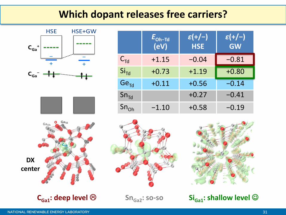
Which dopant releases free carriers?
EOh−Td
(eV) ε(+/−)
HSE ε(+/−)
GW
CTd +1.15 −0.04 −0.81
SiTd +0.73 +1.19 +0.80
GeTd +0.11 +0.56 −0.14
SnTd +0.27 −0.41
SnOh −1.10 +0.58 −0.19
CGa1: deep level SnGa2: so-so SiGa1: shallow level
DX center
32
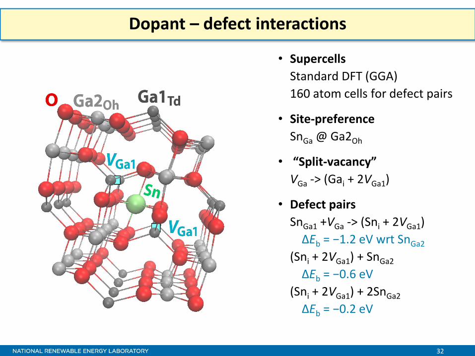
Dopant – defect interactions
• Supercells
Standard DFT (GGA)
160 atom cells for defect pairs
• Site-preference
SnGa @ Ga2Oh
• “Split-vacancy”
VGa -> (Gai + 2VGa1)
• Defect pairs
SnGa1 +VGa -> (Sni + 2VGa1)
ΔEb = −1.2 eV wrt SnGa2
(Sni + 2VGa1) + SnGa2
ΔEb = −0.6 eV
(Sni + 2VGa1) + 2SnGa2
ΔEb = −0.2 eV

33
Defect equilibria
• Net doping (ND − NA) vs. pO2 and c(Sn)
• Solubility limits
• Activated vs. compensated doping
• Isolated defects vs. defect-pairs

34
Sn vs Si and temperature
trends
Dopant choice
• Si slightly less compensated than Sn
Increasing T causes
• Higher solubility limits
• Lower compensation ratio
• Higher limit of dopant conc.
• Higher ND − NA

35
Optimizing experimental conditions
T (C)
log(pO2) (atm)
ND – NA (1020 cm-3)
Si/Si+Ga (1020 cm-3)
in Si cat%
600 -29.2 1.4 11.0 2.9%
700 -22.6 1.0 6.9 1.8%
800 -17.4 0.8 4.5 1.2%
900 -13.0 0.6 3.0 0.8%
1000 -9.2 0.4 2.2 0.6%
DPD: High T, low pO2, optimal dopant conc.
Thermodynamics: High pGa2O causes material loss
Maximal doping: Lower T, optimize pO2 and Si conc.

36
Disordered multinary compounds

37
Multinary compounds: Cu2ZnSnS4 (CZTS) and Cu2SnS3 (CTS)
Cu, Sn
Zn, Cu
Sn, Cu
Cu, Zn
Cu, Sn
S. Chen et al., PRB 81, 245204 (2010) A. Nagoya, PRB 79, 115126 (2009)
• Experiment: Order – disorder phenomena
• Theory: CuZn – ZnCu defect pair
• Description beyond the defect model?

38
Model Hamiltonian: CZTS and Cu2SnS3 (CTS)
Cu Sn S
S-CuiSnjZn4-i-j motifs
S-Cu3Sn
S-Cu2Sn2
D fH = 2 e f ((i, j )
å i, j) n(i, j)
• Motif based Hamiltonian emphasizes local order and octet rule
• Good fit even thought long range order effects are excluded
• Simple Hamiltonian allows efficient Monte-Carlo simulations

39
Entropy-driven clustering in CTS
P. Zawadzki, A. Zakutayev, and S. Lany, Entropy-driven clustering in tetrahedrally bonded multinary materials, Phys. Rev. Appl. 3, 034007 (2015).
Monte Carlo simulations
ordered disordered
S-Cu2Sn2 S-Cu3Sn1
CTS
• Disorder induced clustering
• Weakly temperature dependent

40
Order-disorder transition in CZTS
P. Zawadzki, A. Zakutayev, and S. Lany, Entropy-driven clustering in tetrahedrally bonded multinary materials, Phys. Rev. Appl. 3, 034007 (2015).
Monte Carlo simulations
• Entropy driven clustering amplifies potential fluctuations
S-Cu2SnZn S-Cu2Sn S-CuSnZn2

41
Implication for point defects: “Extended anti-sites”
S-Cu4
CuSn
S-Cu2Sn2
• Formation energy of CuSn reduced by 1.5 eV in disordered CTS
• Point defect model in ordered crystal does not capture energetics of off-stoichiometry
P. Zawadzki, A. Zakutayev, S. Lany, Extended antisite defects in tetrahedrally bonded semiconductors, Phys. Rev. B 92, 201204(R) (2015)
S-Cu3Sn1

42
Cation ordering in ZnSnN2
Zn Sn N
Crystal structure of ordered ZnSnN2 (ZTN)
• Orthorhombic (ORC) cell is supercell of Wurtzite (WZ)
• All N atoms coordinated by 2 Zn and 2 Sn
Zn Sn
N
Zn3Sn1 Sn4 Zn2Sn2
octet-rule conserving

43
ZTN disorder: Phase transition and energies
Disorder vs temperature (model H)
• Ordered ground state: only Zn2Sn2 motifs (octet)
• Around 2000C transition to phase with 40% of Zn3Sn1+Zn1Sn3 motifs
• Zn4 and Sn4 stay below 1%
Energies (DFT)
• Disordered octet-conserving: Essentially degenerate, DH = 0.5 meV/atom, occurs at any temperature
• Average energy is linear in concentration x31 = x13 of Zn3Sn1 motifs

44
Band gap calculations
Approach
• Need to avoid “DFT band gap error”
• Full-fledged GW calculations not feasible for supercells of disordered ZTN
• Use “single-shot” hybrid functional, plus on-site potential U for Zn-d
• Fitting to GW calculation for ZnSnN2, Zn3N2, and Sn3N4
Screening in GW: W = W(r,r’,w)
Hybrid functional: scaling by a < 1
Fit result: a = 0.14, UZn-d = 4 eV
Eg within 0.1 eV, VBM, CBM, Zn-d within 0.2 eV
Eg = 1.41 eV
Eg = 1.45 eV

45
Disorder effects on electronic structure
Band gaps and optical properties
• Valence conserving disorder (only Zn2Sn2 motifs) has virtually no effect, as compared to the perfectly ordered ORC structure
• Band gap shrinks with increasing x31
• Absorption edge becomes less steep

46
Inverse Participation Ratio: Measure of localization
pi(E): atomic density of states For example, IPR=10 means DOS is localized on 1 out of 10 atoms
• Octet-rule conserving disorder is benign
• “31” disorder causes only moderate localization
• Zn4 motifs create localized VB derived gap states
• Total random disorder fills gap with localized defect states

Conclusions
• Electronic structure Many-body perturbation theory in GW approximation Band-gaps, band-structure, optical properties
• Defects Defect formation energies, dopant-defect pair interaction Thermodynamic modeling, “defect phase diagrams”
• Disorder Model-Hamiltonian for total energy: Motif expansion Monte-Carlo simulations for atomic structure Electronic structure for disordered compounds
• http://materials.nrel.gov Database for DFT and GW calculations