
Ch1_figs
34
Figures from CMOS Circuit Design, Layout, and Simulation, Second Edition By R. Jacob Baker, Copyright Wiley-IEEE Define circuit inputs and outputs (Circuit specifications) Hand calculations and schematics Circuit simulations Layout Re-simulate with parasitics Does the circuit meet specs? Does the circuit meet specs? Prototype fabrication Test and evaluate Does the circuit meet specs? Production No Yes Yes No No, spec problem Yes No, fab problem Flowchart for the CMOS IC design process. Figure 1.1
description
baker chapter1 figs
Transcript of Ch1_figs

Figures from CMOS Circuit Design, Layout, and Simulation, Second Edition
By R. Jacob Baker, Copyright Wiley-IEEE
Define circuit inputsand outputs
(Circuit specifications)
Hand calculationsand schematics
Circuit simulations
Layout
Re-simulate with parasitics
Does the circuitmeet specs?
Does the circuitmeet specs?
Prototype fabrication
Test and evaluate
Does the circuitmeet specs?
Production
No
Yes
Yes
No
No, spec problem
Yes
No, fab problem
Flowchart for the CMOS IC design process.Figure 1.1

Figures from CMOS Circuit Design, Layout, and Simulation, Second Edition
By R. Jacob Baker, Copyright Wiley-IEEE
A dice fabricated with other die on the silicon wafer
Top (layout) view
Side (cross-section) view
Enlarged
Wafer diameter is typically 100 to 300 mm.
CMOS integrated circuits are fabricated on and in a silicon wafer.Figure 1.2
200 mm wafer(8 inches)
Figure 1.3 How a chip is packaged (a) and (b) a closer view.
Chip Bond wire Epoxy to holdchip in placeBonding pad(a) (b)

Figures from CMOS Circuit Design, Layout, and Simulation, Second Edition
By R. Jacob Baker, Copyright Wiley-IEEE
Figure 1.4 Plastic packages are used (generally) when the chip is mass produced.
Chips placed on a lead frame.
A plastic "puck"melted to form a package.
Packaged parts prior to bending the pins into place.Final parts sent to customer.
Detail Chip
Figure 1.5 Layout and cross sectional view of a pie (minus pie tin).
Cut pie here
(b) Cross-sectional view
(a) Layout view

Figures from CMOS Circuit Design, Layout, and Simulation, Second Edition
By R. Jacob Baker, Copyright Wiley-IEEE
Figure 1.6 Starting LASI using the MOSIS setups.

Figures from CMOS Circuit Design, Layout, and Simulation, Second Edition
By R. Jacob Baker, Copyright Wiley-IEEE
Figure 1.7 Screen after making a cell called "test" with a rank of 1.
Load or create a cellCell name and rank (clicking on the word or
picture results in the same action)
Reference marker (drawings origin)
Location of the mouse
The mouse can be toggled between a cross andand crosshairs by pressing the tab button.
Toggles displayof the referencemarker

Figures from CMOS Circuit Design, Layout, and Simulation, Second Edition
By R. Jacob Baker, Copyright Wiley-IEEE
Figure 1.8 Navigating in LASI (see text).

Figures from CMOS Circuit Design, Layout, and Simulation, Second Edition
By R. Jacob Baker, Copyright Wiley-IEEE
Figure 1.9 Drawing a box using LASI.

Figures from CMOS Circuit Design, Layout, and Simulation, Second Edition
By R. Jacob Baker, Copyright Wiley-IEEE
Figure 1.10 Showing how the working and dot grids are set in LASI using theCnfg command.
Figure 1.11 Adding the test cell with a rank of 1 to the test2 cell with a rank of 2.
Test cell outline (notice it's small)
Object indicates the test cell

Figures from CMOS Circuit Design, Layout, and Simulation, Second Edition
Figure 1.12 Adding several "test" cells with a rank of 1 to the "test2" cell witha rank of 2.
Figure 1.13 Going back to the "test" cell and adding a additional n-well box.

Figures from CMOS Circuit Design, Layout, and Simulation, Second Edition
By R. Jacob Baker, Copyright Wiley-IEEE
Figure 1.14 How the change to the "test" cell propagates up through the hierarchy.

Figures from CMOS Circuit Design, Layout, and Simulation, Second Edition
By R. Jacob Baker, Copyright Wiley-IEEE
Figure 1.15 Drawing a polygon in LASI on the POL1 (polysilicon) layer.
Vertices of the polygon
Notice

Figures from CMOS Circuit Design, Layout, and Simulation, Second Edition
By R. Jacob Baker, Copyright Wiley-IEEE
Figure 1.16 Closing the polygon in Fig. 1.15 and drawing a path object with a width of 4.
Closing the polygon in Fig. 1.15
Drawing a path with awidth of 4.
Vertices

Figures from CMOS Circuit Design, Layout, and Simulation, Second Edition
By R. Jacob Baker, Copyright Wiley-IEEE
Figure 1.17 Adding text to a layout.
Text vertex

Figures from CMOS Circuit Design, Layout, and Simulation, Second Edition
By R. Jacob Baker, Copyright Wiley-IEEE
Figure 1.18 Setting up the Fkeys to speed up layout.
Figures from CMOS Circuit Design, Layout, and Simulation, Second Edition
By R. Jacob Baker, Copyright Wiley-IEEE
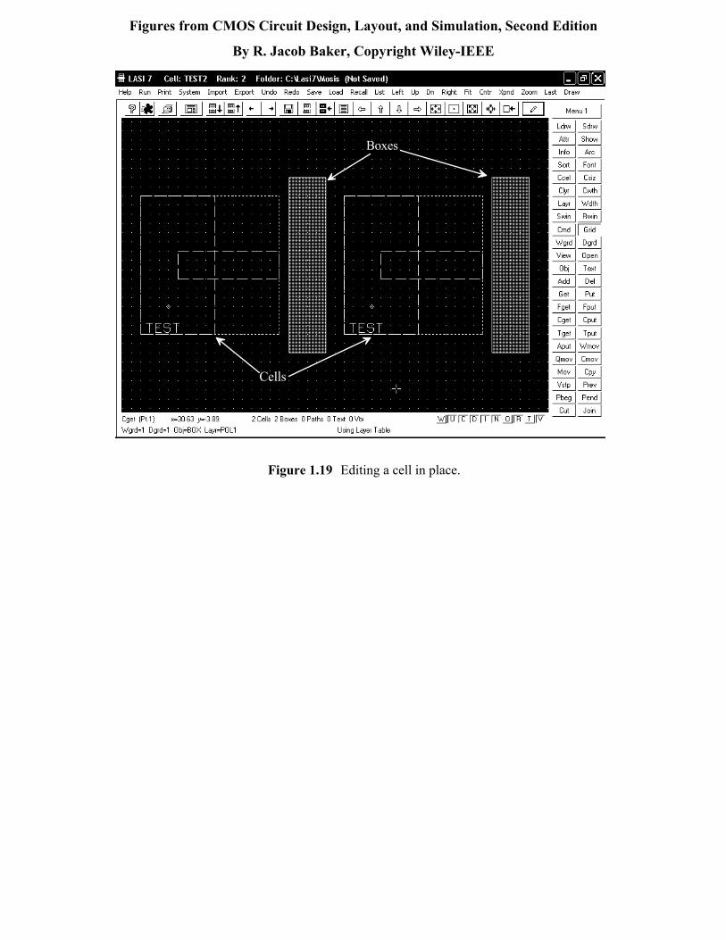
Figure 1.19 Editing a cell in place.
Boxes
Cells

Figures from CMOS Circuit Design, Layout, and Simulation, Second Edition
By R. Jacob Baker, Copyright Wiley-IEEE
Figure 1.20 The LASI System Screen.
Figure 1.21 Generating a GDS file from a TLC file.
Scale factor
Figures from CMOS Circuit Design, Layout, and Simulation, Second Edition
By R. Jacob Baker, Copyright Wiley-IEEE
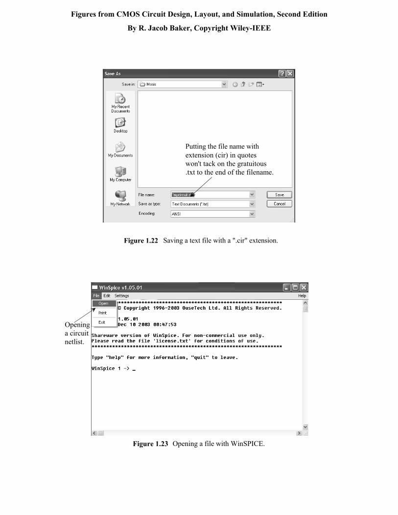
Figure 1.22 Saving a text file with a ".cir" extension.
Putting the file name with extension (cir) in quoteswon't tack on the gratuitous.txt to the end of the filename.
Figure 1.23 Opening a file with WinSPICE.
Openinga circuitnetlist.

Figures from CMOS Circuit Design, Layout, and Simulation, Second Edition
By R. Jacob Baker, Copyright Wiley-IEEE
R1, 1k
R2, 2kVin, 1 V
Vout
Figure 1.24 Simulating the operation of a resistive divider.
Vin
Figure 1.25 Simulating the circuit in Fig. 1.24.
Vin
Vout
Figure 1.26 Simulating the operation of a resistive divider with a sinewave input.
R1, 1k
R2, 2k
VoutVin
Vin1V (peak) at
1 MHz

Figures from CMOS Circuit Design, Layout, and Simulation, Second Edition
By R. Jacob Baker, Copyright Wiley-IEEE
R1, 1k VoutVin
C1,1p
0 to 1 Vdelay 6nstime at 1 V = 3 nsperiod = 10 ns
Figure 1.27 Simulating the step response of an RC circuit using a pulsed source voltage.
1k
1p 1kAn input pulse.
Figure 1.28 Circuit used in Problem 1.16

Figures from CMOS Circuit Design, Layout, and Simulation, Second Edition
By R. Jacob Baker, Copyright Wiley-IEEE
Figure 1.6 Discrete NMOS device from US Patent 3,356,858 [1]. Note the metalgate and the connection to the MOSFET's body on the bottom of the device. Also note that the source and body are tied together.
Figure 1.7 Discrete PMOS device from US Patent 3,356,858 [1].

Figures from CMOS Circuit Design, Layout, and Simulation, Second Edition
By R. Jacob Baker, Copyright Wiley-IEEE
Figure 1.8 Inverter schematic from US Patent 3,356,858 [1].
Figure 1.9 Saving a text file with a ".cir" extension.
Putting the file name with extension (cir) in quoteswon't tack on the gratuitous.txt to the end of the filename.
Figures from CMOS Circuit Design, Layout, and Simulation, Second Edition
By R. Jacob Baker, Copyright Wiley-IEEE
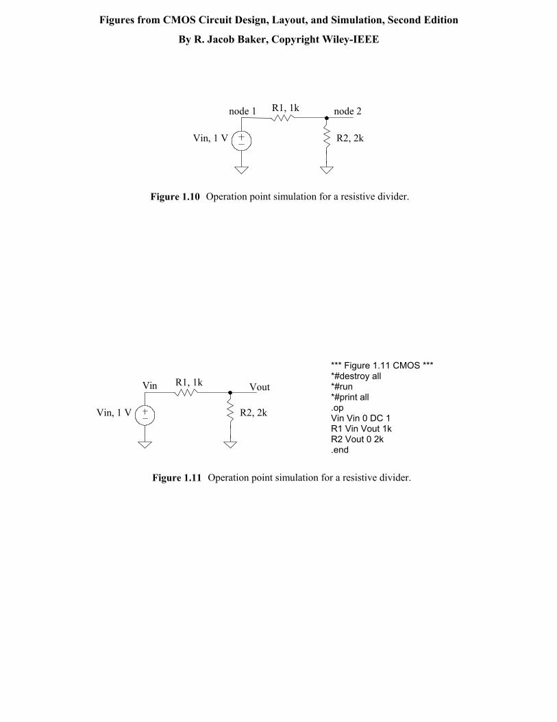
R1, 1k
R2, 2kVin, 1 V
node 2node 1
Figure 1.10 Operation point simulation for a resistive divider.
R1, 1k
R2, 2kVin, 1 V
VoutVin
Figure 1.11 Operation point simulation for a resistive divider.
*** Figure 1.11 CMOS ****#destroy all*#run*#print all.opVin Vin 0 DC 1R1 Vin Vout 1kR2 Vout 0 2k.end

Figures from CMOS Circuit Design, Layout, and Simulation, Second Edition
By R. Jacob Baker, Copyright Wiley-IEEE
R1, 1k
R2, 2kVin, 1 V
Vin
Figure 1.12 Measuring the transfer function in a resistive divider when the outputvariable is the current through R2 and the input is Vin.
Vmeas, 0 V
Vout
I(Vmeas)
*** Figure 1.12 CMOS ****#destroy all*#run*#print all.TF I(Vmeas) VinVin Vin 0 DC 1R1 Vin Vout 1kR2 Vout Vmeas 2kVmeas Vmeas 0 DC 0.end
23
1k
3k
2k
Figure 1.13 Example using a voltage-controlled voltage source.
1V
VinVoutVt
Vb

Figures from CMOS Circuit Design, Layout, and Simulation, Second Edition
By R. Jacob Baker, Copyright Wiley-IEEE
Figure 1.14 Voltage-controlled current source in SPICE.
G, gainn1n2
n3
n4Voltage-Controlled Current Source (VCCS)
G1 n3 n4 n1 n2 G
Figure 1.15 An op-amp simulation example.
VoutVin, 1V
Rin, 1k
Rf, 3k
Vout
Vin, 1V
Rin, 1k
Ideal op-amp
Rf, 3k
1MEG 1 ohm
Figures from CMOS Circuit Design, Layout, and Simulation, Second Edition
By R. Jacob Baker, Copyright Wiley-IEEE
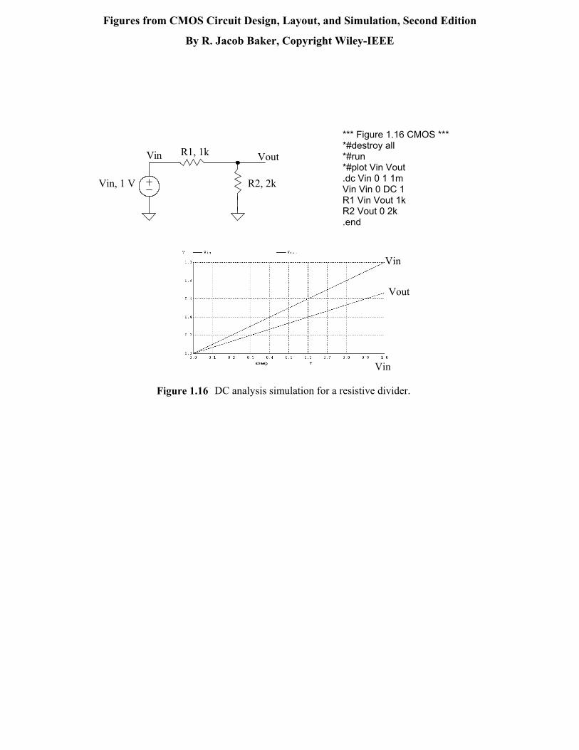
R1, 1k
R2, 2kVin, 1 V
VoutVin
Figure 1.16 DC analysis simulation for a resistive divider.
Vin
Vout
Vin
*** Figure 1.16 CMOS ****#destroy all*#run*#plot Vin Vout.dc Vin 0 1 1mVin Vin 0 DC 1R1 Vin Vout 1kR2 Vout 0 2k.end

Figures from CMOS Circuit Design, Layout, and Simulation, Second Edition
By R. Jacob Baker, Copyright Wiley-IEEE
1k
Vin
Vin
Figure 1.17 Plotting the current-voltage curve for a diode.
VdId
Vd
Id
Vd
*** Figure 1.17 CMOS ****#destroy all*#run*#let ID=-Vin#branch*#plot ID.dc Vin 0 1 1mVin Vin 0 DC 1R1 Vin Vd 1kD1 Vd 0 mydiode.model mydiode D.end
Figure 1.18 Plotting the current-voltage curves for an NPN BJT.
Vce
Vce
Ib
Vb
Ib=15uIb=20uIb=25u
Ib=10uIb=5u
*** Figure 1.18 CMOS ****#destroy all*#run*#let Ic=-Vce#branch*#plot Ic.dc Vce 0 5 1m Ib 5u 25u 5uVce Vce 0 DC 0Ib 0 Vb DC 0Q1 Vce Vb 0 myNPN.model myNPN NPN.end

Figures from CMOS Circuit Design, Layout, and Simulation, Second Edition
By R. Jacob Baker, Copyright Wiley-IEEE
Figure 1.19 Transient simulation for the circuit in Fig. 1.11.
Vin
Vout
Figure 1.20 Simulating a resistive divider with a sinusoidal input.
R1, 1k
R2, 2k
VoutVin
Vin1V (peak) at
1 MHz
*** Figure 1.20 ****#destroy all*#run*#plot vin vout.tran 1n 3u Vin Vin 0 DC 0 SIN 0 1 1MEGR1 Vin Vout 1kR2 Vout 0 2k.end

Figures from CMOS Circuit Design, Layout, and Simulation, Second Edition
By R. Jacob Baker, Copyright Wiley-IEEE
Figure 1.21 Simulating the operation of an RC circuit using a .tran analysis.
R, 1k VoutVin
Vin1V (peak) at
200 Hz
C, 1uF
Vin Vout
*** Figure 1.21 ****#destroy all*#run*#plot vin vout.tran 10u 30mVin Vin 0 DC 0 SIN 0 1 200R1 Vin Vout 1kCL Vout 0 1u.end
Figure 1.22 Another RC circuit example.
R, 1k
VoutVin
Vin1V (peak) at
200 Hz
C2, 1uF
C1, 2uF
*** Figure 1.22 ****#destroy all*#run*#plot vin vout.tran 10u 30mVin Vin 0 DC 0 SIN 0 1 200R1 Vin Vout 1kC1 Vin Vout 2uC2 Vout 0 1u.end
Figures from CMOS Circuit Design, Layout, and Simulation, Second Edition
By R. Jacob Baker, Copyright Wiley-IEEE
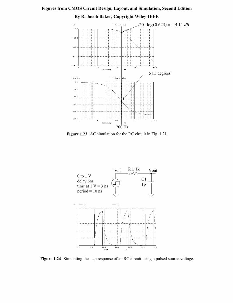
Figure 1.23 AC simulation for the RC circuit in Fig. 1.21.
51.5 degrees
200 Hz
20 ⋅ log (0.623) = − 4.11 dB
R1, 1k VoutVin
C1,1p
0 to 1 Vdelay 6nstime at 1 V = 3 nsperiod = 10 ns
Figure 1.24 Simulating the step response of an RC circuit using a pulsed source voltage.

Figures from CMOS Circuit Design, Layout, and Simulation, Second Edition
By R. Jacob Baker, Copyright Wiley-IEEE
Figure 1.25 Specifying a rise time in the pulse statement to avoid slow rise times(rise times set by the maximum step size in the .tran statement.)
Figure 1.26 Step response of an RC circuit.
Figure 1.27 Another step response (negative going) of an RC circuit.

Figures from CMOS Circuit Design, Layout, and Simulation, Second Edition
By R. Jacob Baker, Copyright Wiley-IEEE
Figure 1.28 Using a PWL source to drive an RC circuit.
R1, 1k VoutVin
C1,1pPWLPWL 0 0.5 3n 1 5n 1 5.5n 0 7n 0
VinVout
s1 node1 node2 controlp controlm switmod
The switch is closed when the node voltage controlp is greater than the node voltage controlm
Figure 1.29 Modeling a switch in SPICE.
node1 node2s1 ron

Figures from CMOS Circuit Design, Layout, and Simulation, Second Edition
By R. Jacob Baker, Copyright Wiley-IEEE
Figure 1.30 Using initial conditions and a switch in an RC circuit simulation.
R1, 1k VoutVin
C1,1p Initially at 2V
At t=2ns switch closes
5 V
*** Figure 1.30 ***
*#destroy all*#run*#plot vout
.tran 100p 8n UIC
Vclk clk 0 pulse -1 1 2nVin Vin 0 DC 5S1 Vin Vouts clk 0 switmodelR1 Vouts Vout 1k C1 Vout 0 1p IC=2
.model switmodel sw ron=0.1
.end
Figure 1.31 Using initial conditions in an inductive circuit.
R1, 1k VoutVin
At t=2ns switch opens
5 V 10 uH
(assume switch was closed for a long time.)
1k
*** Figure 1.31 ***
*#destroy all*#run*#plot vout
.tran 100p 8n UIC
Vclk clk 0 pulse -1 1 2nVin Vin 0 DC 5S1 Vin Vouts 0 clk switmodelR1 Vouts Vout 1k R2 Vout 0 1kL1 Vout 0 10u IC=5m
.model switmodel sw ron=0.1
.end

Figures from CMOS Circuit Design, Layout, and Simulation, Second Edition
By R. Jacob Baker, Copyright Wiley-IEEE
Figure 1.32 Determining the Q, or quality factor, of an LC tank.
Vout
AC 1 10 nH1k 10 pF
*** Figure 1.32 ***
*#destroy all*#run*#plot db(vout)
.AC lin 100 400MEG 600MEG
Iin Vout 0 DC 0 AC 1R1 Vout 0 1k L1 Vout 0 10nC1 Vout 0 10p
.end
Figure 1.33 An integrator example.
Vout
1k
1uF
Vin
*** Figure 1.33 ***
*#destroy all*#run*#plot db(vout/vin)*#set units=degrees*#plot ph(vout/vin)
.ac dec 100 1 10k
Vin Vin 0 DC 1 AC 1Rin Vin vm 1kCf Vout vm 1u
X1 Vout 0 vm Ideal_op_amp.subckt Ideal_op_amp Vout Vp VmG1 Vout 0 Vm Vp 1MEGRL Vout 0 1.ends.end

Figures from CMOS Circuit Design, Layout, and Simulation, Second Edition
By R. Jacob Baker, Copyright Wiley-IEEE
Figure 1.34 Time-domain integrator example.
Vout
1k
1uF
Vin
*** Figure 1.34 ***
*#destroy all*#run*#plot vout vin
.tran 10u 10m
.ic v(vout)=0
Vin Vin 0 DC 1 + pulse -1 1 0 1u 1u 2m 4mRin Vin vm 1kCf Vout vm 1u
X1 Vout 0 vm Ideal_op_amp.subckt Ideal_op_amp Vout Vp VmG1 Vout 0 Vm Vp 1MEGRL Vout 0 1.ends.end


