Ceramic Capacitor Technology - TDK Electronics · 15,8 0,00 15,8 Ceramic Capacitor Technology...
30
Ceramic Capacitor Technology CeraLink™ Opens New Dimensions in Power Electronics EPCOS AG A TDK Group Company PPD Business Group Germany September 2018
Transcript of Ceramic Capacitor Technology - TDK Electronics · 15,8 0,00 15,8 Ceramic Capacitor Technology...
15,815,8 0,00
Ceramic Capacitor Technology
CeraLink™ Opens New Dimensions
in Power Electronics
EPCOS AG
A TDK Group Company
PPD Business Group
Germany
September 2018
Ceramic Capacitor Technology CeraLinkTM
15,815,8 0,00
© EPCOS AG A TDK Group Company 2018
PPD 08/18 2
5,60
Ceramic Capacitor Technology

Ceramic Capacitor Technology CeraLinkTM
15,815,8 0,00
© EPCOS AG A TDK Group Company 2018
PPD 08/18 3
5,60
PLZT – a highly flexible ceramic material class
5,60
Piezo actuators Capacitors
Ceramic Capacitor Technology CeraLinkTM
15,815,8 0,00
© EPCOS AG A TDK Group Company 2018
PPD 08/18 4
5,60
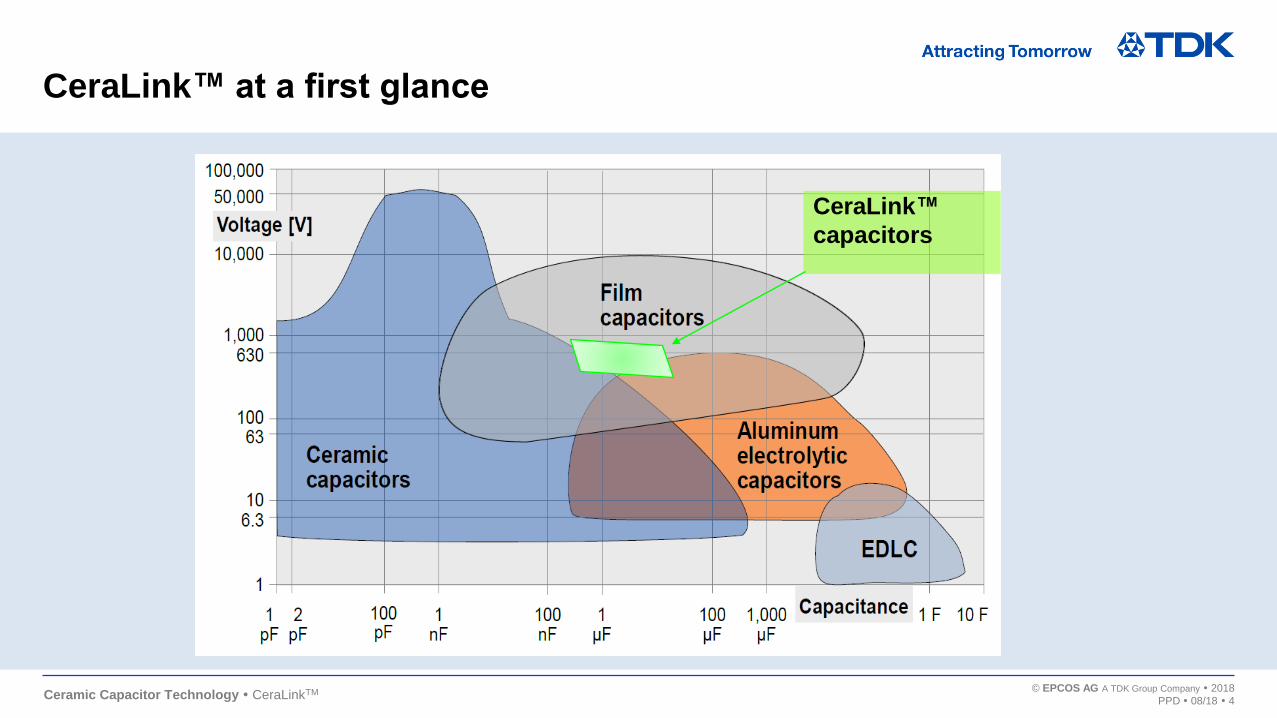
CeraLink™ at a first glance
CeraLink™
capacitors

Ceramic Capacitor Technology CeraLinkTM
15,815,8 0,00
© EPCOS AG A TDK Group Company 2018
PPD 08/18 5
5,60
CeraLink™ at a first glance
Ceramic Capacitor Technology CeraLinkTM
15,815,8 0,00
© EPCOS AG A TDK Group Company 2018
PPD 08/18 6
5,60
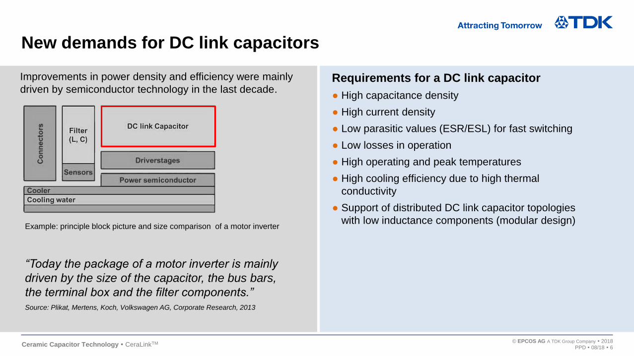
New demands for DC link capacitors
Requirements for a DC link capacitor
High capacitance density
High current density
Low parasitic values (ESR/ESL) for fast switching
Low losses in operation
High operating and peak temperatures
High cooling efficiency due to high thermal
conductivity
Support of distributed DC link capacitor topologies
with low inductance components (modular design)
Improvements in power density and efficiency were mainly
driven by semiconductor technology in the last decade.
Example: principle block picture and size comparison of a motor inverter
“Today the package of a motor inverter is mainly
driven by the size of the capacitor, the bus bars,
the terminal box and the filter components.”Source: Plikat, Mertens, Koch, Volkswagen AG, Corporate Research, 2013

Ceramic Capacitor Technology CeraLinkTM
15,815,8 0,00
© EPCOS AG A TDK Group Company 2018
PPD 08/18 7
5,60
Technology guideline
5,60
Film Capacitor Large MLCC Chips Stacked MLCC CeraLink
• more compact
• higher operating
temperature
• lower ESL
• higher frequency
• SMD
• higher ripple
current ratings
• more compact
/ less footprint
• lower ESL
• more robust
• higher cap-density
at Vop
• higher operating
temperature
• lower ESL
• higher ripple
current ratings
Standard semiconductor
technologyStandard semiconductor
technology
Enhanced technologies / modular
ceramic designs possible /
automotive
High-end and high-temperature
applications / fast switching (SiC) / full
cermic DC-link solutions

Ceramic Capacitor Technology CeraLinkTM
15,815,8 0,00
© EPCOS AG A TDK Group Company 2018
PPD 08/18 8
5,60
How does CeraLink™ meet these requirements?
Material Ceramic chip
features
Packaging
High capacitance
density
High current
densityLow parasitic
values
Low losses
High operating and
peak temperatures
High cooling
efficiency
Modular design

Ceramic Capacitor Technology CeraLinkTM
15,815,8 0,00
© EPCOS AG A TDK Group Company 2018
PPD 08/18 9
5,60
Material
PLZT – an antiferroelectric material
P Dielectric polarization
E Electrical field strength
ε Permittivity
P
E
E
ε
P
E
E
ε
P
E
E
ε
Linear Ferroelectric Antiferroelectric
Nature of electrical
polarizationElectronic, ionic
Permanent dipoles form
ferroelectric domains
Permanent dipoles form
antiparallel zones
Material class (Ba,Nd)TiO, typ. NP0, C0G BaTiO3 (BTO), typ. X7R (Pb,La)(Zr,Ti)O3 (PLZT)
Advantagesε constant over electric field
and temperatureε up to 10,000 is possible
ε increases with field
Disadvantages ε < 100ε decreases strongly with
electrical fieldε low at zero bias

Ceramic Capacitor Technology CeraLinkTM
15,815,8 0,00
© EPCOS AG A TDK Group Company 2018
PPD 08/18 10
5,60
High capacitance density at operating condition
Due to antiferroelectic behavior, the
characteristics of CeraLink™ are strongly
non-linear and optimized for conditions
under operation in power electronics
Film capacitors and class 1 ceramics have
a dielectric constant (nearly) independent
on the electrical field. (ε < 100)
The permittivity of ferroelectric (e.g. X7R)
MLCC capacitors is decreasing with
electrical field
CeraLink™ features an increasing dielecric
constant up to the operating voltage
At higher AC voltage (peaks), the material
is able to provide even higher permittivies
DC bias characteristics at room temperature
4000
3000
2000
1,000
0
Die
ele
ctr
icc
on
sta
nt
Electric
field [V/µm]0 2 4 6 8 10 12
Film
capacitor
Class 2
MLCCCeraLink™
Nominal / rated capacitance 100 % 100 % 100 %
No bias voltage 0.5 VRMS 100% 100 % 35 %
DC link voltage 0.5 VRMS 100 % 35 % 60 %
DC link voltage 20 VRMS 100 % 35 % 100 %
DC link (energy)
Snubber

Ceramic Capacitor Technology CeraLinkTM
15,815,8 0,00
© EPCOS AG A TDK Group Company 2018
PPD 08/18 11
5,60
CeraLink™ is ideal for fast switching
Device characteristics lead to a low inductive
commutation loop
High capacitance density of 2 to 5 µF/cm³
Low self-inductance (ESL) of 2.5 to 4 nH
High thermal robustness allows CeraLink™ to be
placed very close to the semi-conductor with
operation up to 150 °C permissible
No limitation of dV/dt
<<ESL
<<Lσ
0
10
20
30
40
50
60
70
80
90
100
0
100
200
300
400
500
600
Time [ns]
CeraLink™
Se
mic
on
du
cto
r s
wit
ch
ing
vo
lta
ge
[V
]
Se
mic
on
co
llec
tor
cu
rren
t[A
]
0 1600 3200 4800 6400 8000 9600
Semiconductor overshoot principle

Ceramic Capacitor Technology CeraLinkTM
15,815,8 0,00
© EPCOS AG A TDK Group Company 2018
PPD 08/18 12
Ceramic Chip Features
Design for robustness against ceramic cracks
MLSC design
Series connection of two MLCC geometries in
one component.
MLSC design prevents short circuits caused
by cracks from mechanical overstress
99
80
60
40
20
10
5
3
2
1
Failu
re [
%]
Rated
voltage
500 V
Voltage [V DC]15001000900800700600500400
Breakdown voltage measurement
Weibull – 95% CI
Shape 21.62
Scale 1331
N 30
AD 0.175
P value >0.250
500 V Chip
zero bias maximum bias
stress in corner
area scales with
height of chip
MFD design
Chip is segmented in height to reduce piezoelectric stress
between active and inactive area

Ceramic Capacitor Technology CeraLinkTM
15,815,8 0,00
© EPCOS AG A TDK Group Company 2018
PPD 08/18 13
5,60
Ceramic chip design for high current capability
and high thermal conductivity
Copper inner electrodes
Co-firing of PLZT ceramic material together with Cu is difficult, but possible
Cu – process is one core competence of the piezo mother factory in Deutschlandsberg, Austria
Cross section of the CeraLink™ multilayer chip consisting of appr. 80 dielectric ceramic layers

Ceramic Capacitor Technology CeraLinkTM
15,815,8 0,00
© EPCOS AG A TDK Group Company 2018
PPD 08/18 14
5,60
Packaging
Robust interconnection of metallic contacts
Lead frame
10,000 cycles thermal
shock test
(-55 °C to +150 °C)
Silver sinter connection between ceramic body and lead frame
Outer contacts made of CIC (copper invar* copper), to combine high
electrical and thermal conductivity with low coefficient of thermal expansion
All materials are excellent thermal and electrical conductors (lowest thermal
and electrical resistance)
Silver layer prevents cracking of the ceramic in case of mechanical
overstress or solder shock open mode!
No crack or damage
after thermal cycles
*Invar: 36Ni-Fe
Ceramic with inner
electrodes (Cu)
Ag galvanic layer
Sintered silver layer

Ceramic Capacitor Technology CeraLinkTM
15,815,8 0,00
© EPCOS AG A TDK Group Company 2018
PPD 08/18 15
5,60
Low losses at high temperatures and frequencies
Low dielectric loss at high temperatures Minimal ESR due to low-loss
copper electrodes and HF-suited backend
Comparison @ 0.1 VAC, 0 VDC, 25 °CComparison @ 1 VAC, 1 kHz, 400 VDC, 25 °C
1µF
MLCC 1µF
extrapolated
ESR @ 100°C,
400VDC
Temperature (°C)
Dis
sip
ati
on
fa
cto
rta
n δ
[10
-3]
Frequency (Hz)
Eq
uiv
ale
nt
se
rie
sre
sis
tan
ce
[Ω]
100500-50 1500
20
40
60
80 10-0
104
10-1
10-2
10-3
105 106 107
BTO = barium titanate oxide = standard MLCC material
Ceramic Capacitor Technology CeraLinkTM
15,815,8 0,00
© EPCOS AG A TDK Group Company 2018
PPD 08/18 16
5,60
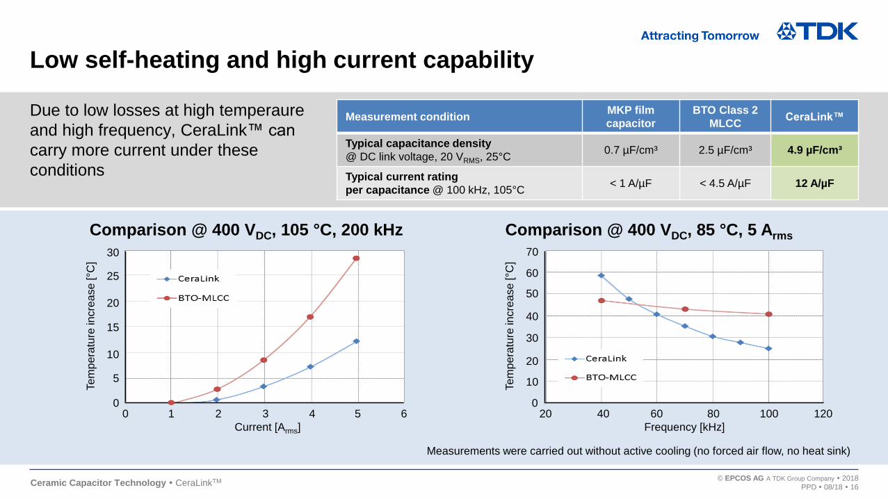
Low self-heating and high current capability
Due to low losses at high temperaure
and high frequency, CeraLink™ can
carry more current under these
conditions
Measurement conditionMKP film
capacitor
BTO Class 2
MLCCCeraLink™
Typical capacitance density
@ DC link voltage, 20 VRMS, 25°C0.7 µF/cm³ 2.5 µF/cm³ 4.9 µF/cm³
Typical current rating
per capacitance @ 100 kHz, 105°C< 1 A/µF < 4.5 A/µF 12 A/µF
Comparison @ 400 VDC, 105 °C, 200 kHz Comparison @ 400 VDC, 85 °C, 5 Arms
5
0 0
Te
mp
era
ture
incre
ase
[°C
]
Te
mp
era
ture
incre
ase
[°C
]
Frequency [kHz]Current [Arms]
0 1 2 3 4 5 6 20 40 60 80 120100
10
15
20
25
30
10
20
30
40
50
60
70
Measurements were carried out without active cooling (no forced air flow, no heat sink)

Ceramic Capacitor Technology CeraLinkTM
15,815,8 0,00
© EPCOS AG A TDK Group Company 2018
PPD 08/18 17
5,60
Exceptional lifetime at high temperatures
Lifetime @ 200 °C three orders of magnitude higher than
that of conventional ceramic capacitors

Ceramic Capacitor Technology CeraLinkTM
15,815,8 0,00
© EPCOS AG A TDK Group Company 2018
PPD 08/18 18
5,60
Lifetime at high temperatures –
comparison of ceramic capacitors
CeraLink™
CeraLink™ offers highest lifetime and capacitance density
compared to conventional ceramic capacitors

Ceramic Capacitor Technology CeraLinkTM
15,815,8 0,00
© EPCOS AG A TDK Group Company 2018
PPD 08/18 19
5,60
Low leakage current at high temperatures
CeraLink™ shows stable and outstanding high
isolation properties compared to all existing
capacitor technologies
low leakage current at elevated temperatures
even above 150°C
No thermal runaway observed for CeraLink™
ceramic material
Comparison @ 400 VDC
1µF
1µF
Temperature [°C]
ρ[Ω
m]
1013
1012
1011
1010
20 40 60 80 120100 140 160
Ceramic Capacitor Technology CeraLinkTM
15,815,8 0,00
© EPCOS AG A TDK Group Company 2018
PPD 08/18 20
5,60
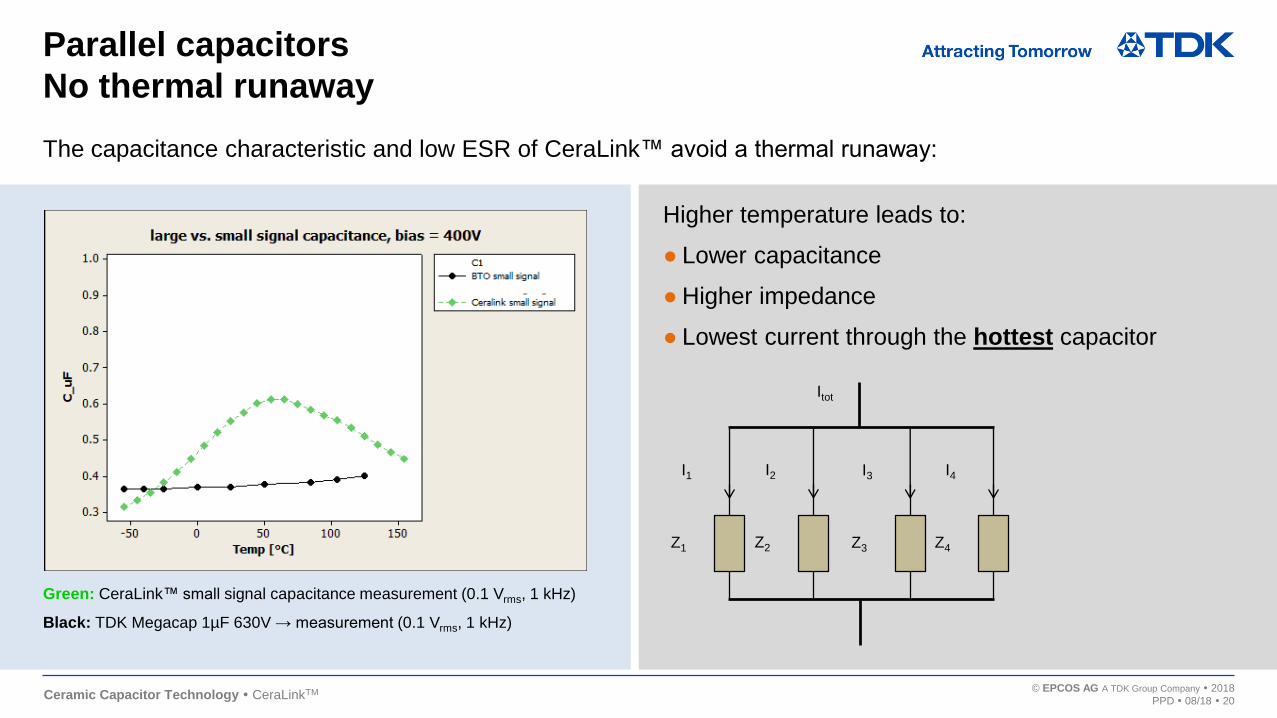
Parallel capacitors
No thermal runaway
The capacitance characteristic and low ESR of CeraLink™ avoid a thermal runaway:
Itot
Z4
I4
Z1
I1
Z2
I2
Z3
I3
Green: CeraLink™ small signal capacitance measurement (0.1 Vrms, 1 kHz)
Black: TDK Megacap 1µF 630V → measurement (0.1 Vrms, 1 kHz)
Higher temperature leads to:
Lower capacitance
Higher impedance
Lowest current through the hottest capacitor

Ceramic Capacitor Technology CeraLinkTM
15,815,8 0,00
© EPCOS AG A TDK Group Company 2018
PPD 08/18 21
5,60
CeraLink™ Product portfolio – modular design
500 V(for 650 V semiconductors)
700 V(for 900 V semiconductors)
900 V(for 1300 V semiconductors)
SP
(20 chips)
LPLP
J-leads
Basic element (chip)
7.85 mm x 6.84 mm x 2.65 mm
Released / To be released soon
FA
(2-10 chips)
Ceramic Capacitor Technology CeraLinkTM
15,815,8 0,00
© EPCOS AG A TDK Group Company 2018
PPD 08/18 22
5,60
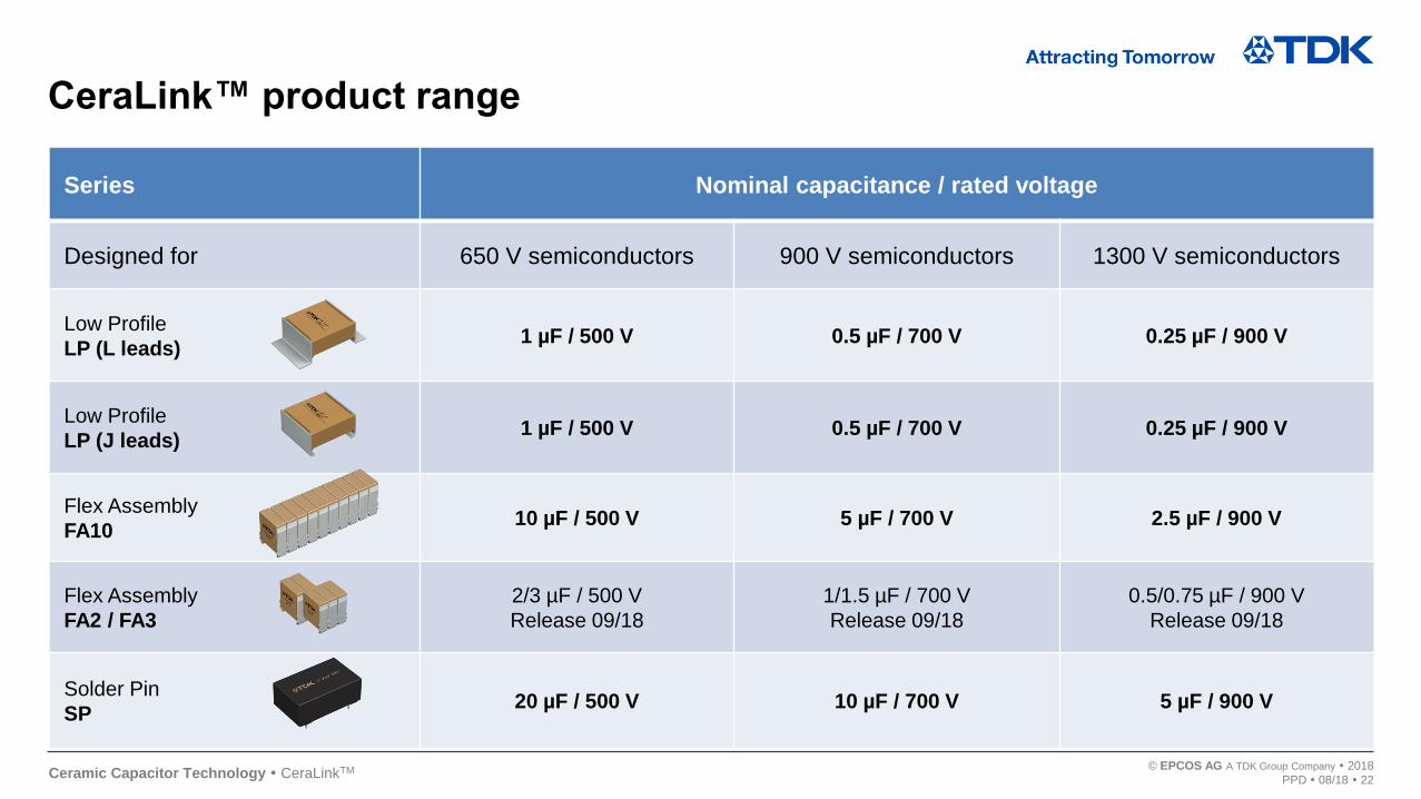
CeraLink™ product range
Series Nominal capacitance / rated voltage
Designed for 650 V semiconductors 900 V semiconductors 1300 V semiconductors
Low Profile
LP (L leads)1 µF / 500 V 0.5 µF / 700 V 0.25 µF / 900 V
Low Profile
LP (J leads)1 µF / 500 V 0.5 µF / 700 V 0.25 µF / 900 V
Flex Assembly
FA1010 µF / 500 V 5 µF / 700 V 2.5 µF / 900 V
Flex Assembly
FA2 / FA3
2/3 µF / 500 V
Release 09/18
1/1.5 µF / 700 V
Release 09/18
0.5/0.75 µF / 900 V
Release 09/18
Solder Pin
SP20 µF / 500 V 10 µF / 700 V 5 µF / 900 V
Ceramic Capacitor Technology CeraLinkTM
15,815,8 0,00
© EPCOS AG A TDK Group Company 2018
PPD 08/18 23
5,60
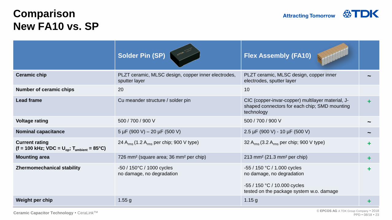
Comparison
New FA10 vs. SP
Solder Pin (SP) Flex Assembly (FA10)
Ceramic chip PLZT ceramic, MLSC design, copper inner electrodes,
sputter layer
PLZT ceramic, MLSC design, copper inner
electrodes, sputter layer~
Number of ceramic chips 20 10
Lead frame Cu meander structure / solder pin CIC (copper-invar-copper) multilayer material, J-
shaped connectors for each chip; SMD mounting
technology
+
Voltage rating 500 / 700 / 900 V 500 / 700 / 900 V ~
Nominal capacitance 5 µF (900 V) – 20 µF (500 V) 2.5 µF (900 V) - 10 µF (500 V) ~
Current rating
(f = 100 kHz; VDC = Uop; Tambient = 85°C)
24 Arms (1.2 Arms per chip; 900 V type) 32 Arms (3.2 Arms per chip; 900 V type) +
Mounting area 726 mm² (square area; 36 mm² per chip) 213 mm² (21.3 mm² per chip) +
Zhermomechanical stability -50 / 150°C / 1000 cycles
no damage, no degradation
-55 / 150 °C / 1.000 cycles
no damage, no degradation
-55 / 150 °C / 10.000 cycles
tested on the package system w.o. damage
+
Weight per chip 1.55 g 1.15 g +
Ceramic Capacitor Technology CeraLinkTM
15,815,8 0,00
© EPCOS AG A TDK Group Company 2018
PPD 08/18 24
5,60
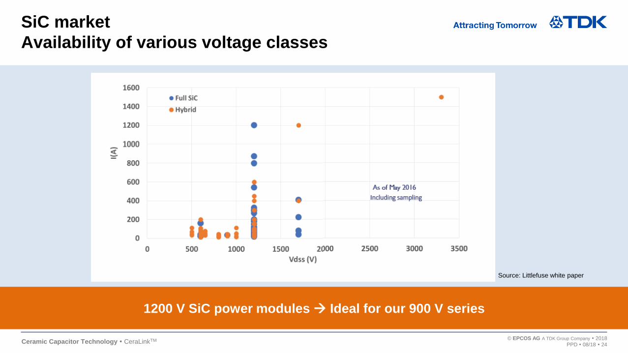
1200 V SiC power modules Ideal for our 900 V series
SiC market
Availability of various voltage classes
Source: Littlefuse white paper

Ceramic Capacitor Technology CeraLinkTM
15,815,8 0,00
© EPCOS AG A TDK Group Company 2018
PPD 08/18 25
5,60
Application example - Industry
Integrated servo drive
Temperature Low ESL
Traditional design Integrated servo drive
… electronics is integrated
into the motor housing
… SiC for new designs

Ceramic Capacitor Technology CeraLinkTM
15,815,8 0,00
© EPCOS AG A TDK Group Company 2018
PPD 08/18 26
5,60 5,60
Application example - Automotive
Onboard chargers
Recommended products (selection)
1. Chip NTCs (thermal sensing against overheating)
- B57232V5103+360
- B57332V5103+360
- NTCG164LH104H
2. Chip varistors (ESD protection for data lines)
- CT0402S17AG
- CT0603L25HSG
- AVRM1608C270MT*
3. Chip varistors (low voltage surge protection)
- CT0805S14BAUTOG
- CT1206S14BAUTOG
- CT2220K30G
- AVRM2012C390KT6AB
4. Leaded varistors (high voltage surge protection)
- SNF14K***E2K1
- SNF20K***E2K1
5. Surge arresters (high voltage protection)
- EHV6*-H…B1-B7
- EHV60-H…SMD
6. PTC ICLs (inrush current protection)
- J21x series
7. CeraLink™ (DC link capacitor or output filtering)
- B58031*
- Flex Assembly FA2 or FA3
CeraLink™
capacitor
Chip varistors
for data-lines
ESD protection
Chip varistors
for battery lines
for surge protection
Chip NTCs for
temperature
sensing
Leaded varistors
for high-voltage
surge protection
PTC ICLs for
inrush current
protection
Surge arresters
for high voltage
protection
CeraLink™ as DC
link capacitor or
output filtering
Example
Ceramic Capacitor Technology CeraLinkTM
15,815,8 0,00
© EPCOS AG A TDK Group Company 2018
PPD 08/18 27
5,60
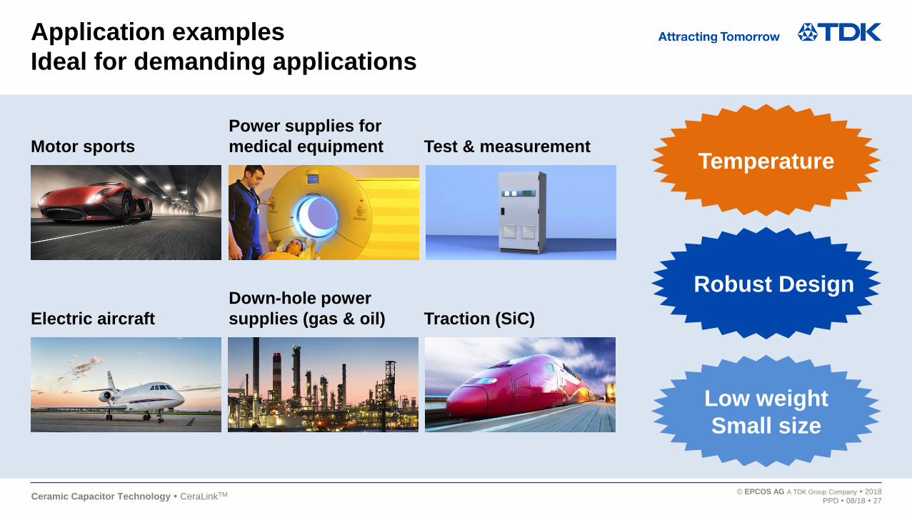
Application examples
Ideal for demanding applications
Motor sportsTemperature
Robust Design
Low weight
Small size
Electric aircraft
Power supplies for
medical equipment
Down-hole power
supplies (gas & oil)
Test & measurement
Traction (SiC)
Ceramic Capacitor Technology CeraLinkTM
15,815,8 0,00
© EPCOS AG A TDK Group Company 2018
PPD 08/18 28
5,60
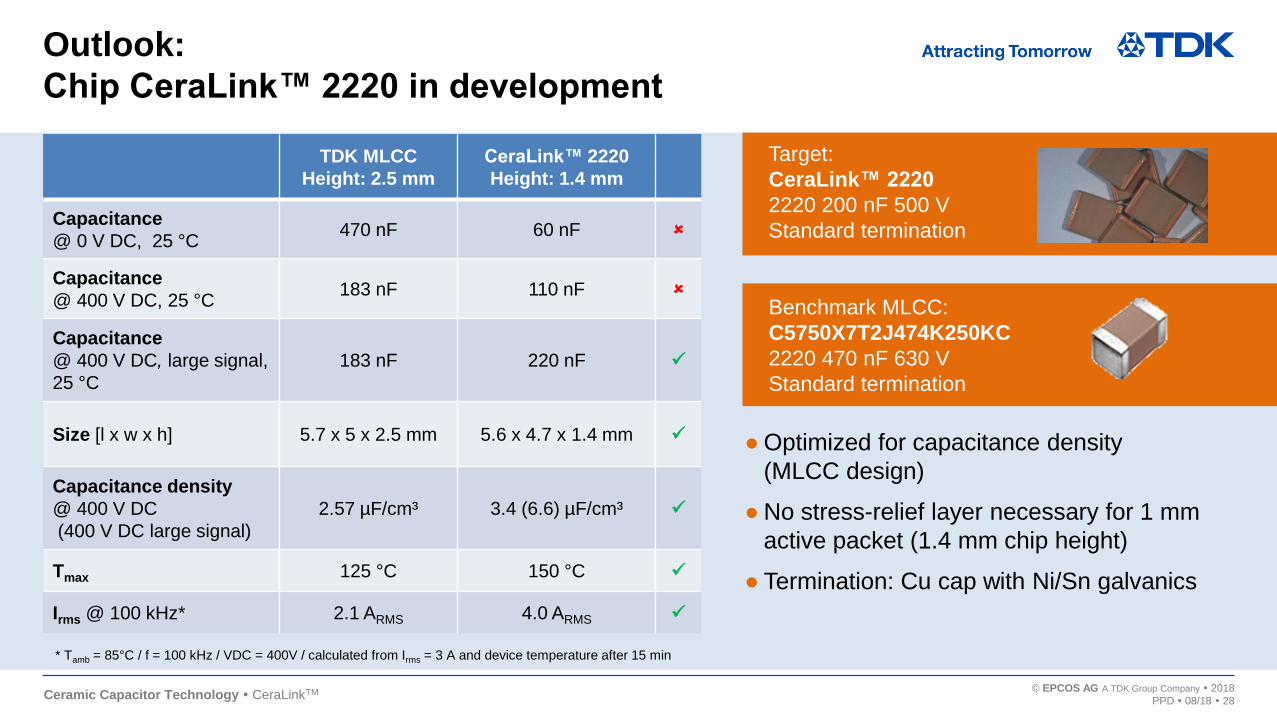
Outlook:
Chip CeraLink™ 2220 in development
TDK MLCC
Height: 2.5 mm
CeraLink™ 2220
Height: 1.4 mm
Capacitance
@ 0 V DC, 25 °C470 nF 60 nF
Capacitance
@ 400 V DC, 25 °C183 nF 110 nF
Capacitance
@ 400 V DC, large signal,
25 °C
183 nF 220 nF
Size [l x w x h] 5.7 x 5 x 2.5 mm 5.6 x 4.7 x 1.4 mm
Capacitance density
@ 400 V DC
(400 V DC large signal)
2.57 µF/cm³ 3.4 (6.6) µF/cm³
Tmax 125 °C 150 °C
Irms @ 100 kHz* 2.1 ARMS 4.0 ARMS
Benchmark MLCC:
C5750X7T2J474K250KC
2220 470 nF 630 V
Standard termination
Target:
CeraLink™ 2220
2220 200 nF 500 V
Standard termination
* Tamb = 85°C / f = 100 kHz / VDC = 400V / calculated from Irms = 3 A and device temperature after 15 min
Optimized for capacitance density
(MLCC design)
No stress-relief layer necessary for 1 mm
active packet (1.4 mm chip height)
Termination: Cu cap with Ni/Sn galvanics
Ceramic Capacitor Technology CeraLinkTM
15,815,8 0,00
© EPCOS AG A TDK Group Company 2018
PPD 08/18 29
5,60
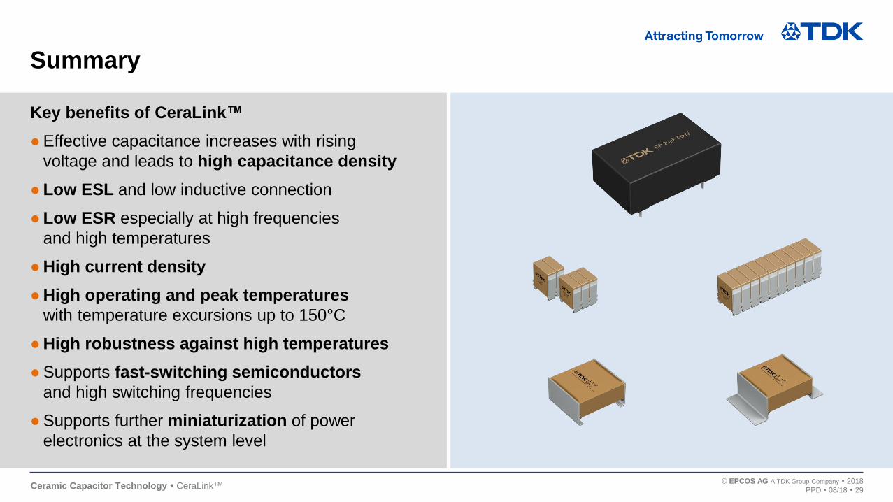
Key benefits of CeraLink™
Effective capacitance increases with rising
voltage and leads to high capacitance density
Low ESL and low inductive connection
Low ESR especially at high frequencies
and high temperatures
High current density
High operating and peak temperatures
with temperature excursions up to 150°C
High robustness against high temperatures
Supports fast-switching semiconductors
and high switching frequencies
Supports further miniaturization of power
electronics at the system level
Summary

15,815,8 0,00
www.global.tdk.com • www.epcos.com