CEO Welcome and NANIUM Overview - SEMI.ORG | CEO...CEO Welcome and NANIUM Overview JUNE 2015 Nanium...
21
CEO Welcome and NANIUM Overview JUNE 2015
Transcript of CEO Welcome and NANIUM Overview - SEMI.ORG | CEO...CEO Welcome and NANIUM Overview JUNE 2015 Nanium...

CEO Welcome and
NANIUM Overview
JUNE 2015

Nanium · SEMI Tech Seminar, June 2015 - Confidential
Located halfway between the US and Asia, we offer all
the European advantages at competitive cost
2
Located in the west coast of Portugal,
NANIUM is the largest OSAT in Europe

Nanium · SEMI Tech Seminar, June 2015 - Confidential
In-house services to enable products from concept
to market
3
Nanium · SEMI Tech Seminar, June 2015 - Confidential
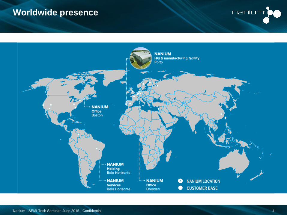
Worldwide presence
4
NANIUM LOCATION
CUSTOMER BASE
NANIUM LOCATION
CUSTOMER BASE

Nanium · SEMI Tech Seminar, June 2015 - Confidential
Service offer and strengths
5
THE WAFER-LEVEL
PACKAGE SOLUTION
PROVIDER
WLCSP
WL3D WLSiP
WLFO

Nanium · SEMI Tech Seminar, June 2015 - Confidential 6
WLP is growing faster than industry

Nanium · SEMI Tech Seminar, June 2015 - Confidential 7
An increasingly connected World

Nanium · SEMI Tech Seminar, June 2015 - Confidential
Key Diff.
factors Why Example of products
Feature Size
Wafer Level Package (both WLCSP and
WLFO) offers the smallest package form-factor
Frequency
Speed Capable of operating at Very High Frequency
Fab Location
Secure and Safe environment
Highest level of IP protection
Encryption, Biometric Validation…….
Integration
WLSiP, WL3D:
Heterogeneous integration (Silicon, GaN, GaAs)
Passives integration, die partitioning, sensors
NANIUM Differentiating in Target Markets
8

Nanium · SEMI Tech Seminar, June 2015 - Confidential
PAST 2014 2015 2016-18
WB-SD-wBGA
WLCSP
WLPOP/ WL3D-1
WB-MD-wBGA
WLCSP+
WLSIP/ WLPIP
WLMCM
WL3D-F2F
WLFO-POP
SS-ML-WLFO SS-SL-WLFO-BGA
SS-SL-WLFO-LGA WB-SD-BGA
WB-MD-BGA
DS-WLFO/ WLSIP
WLPOP/ WL3D-2
WB-RDL
WLSTACK
Fan-In WLP
Fan-Out WLP/ Embedding
NANIUM Package Roadmap
9

Nanium · SEMI Tech Seminar, June 2015 - Confidential
9x8mm² 8x8mm²
5x5mm²
Sensor Integration
Embedded Wafer-Level System Integration
10

Nanium · SEMI Tech Seminar, June 2015 - Confidential
The Worlds Largest WLCSP in Volume
Main Features:
- 25mm x 23mm, 28nm CMOS GF (5.5 bn transistors)
- ASIC, consumes in peak load hundreds of Watt
- 1,188 BGA I/O-Matrix 380um balls w/ 700um pitch
- Special TCoB optimized solder ball alloy
- Reliability tests w/ fully connected Daisy Chain, no UF
- Tested with 2 dielectric materials (PBO and PI)
- PBO: Passed 400 TCoB (IPC-9701 – TC2)
- PI: Passed 600 TCoB (IPC-9701 – TC2)
11

Thank you for
your attention
NANIUM S.A.
Avenida 1º de Maio 801
4485-629 Vila do Conde
Portugal
Nanium · SEMI Tech Seminar, June 2015 - Confidential
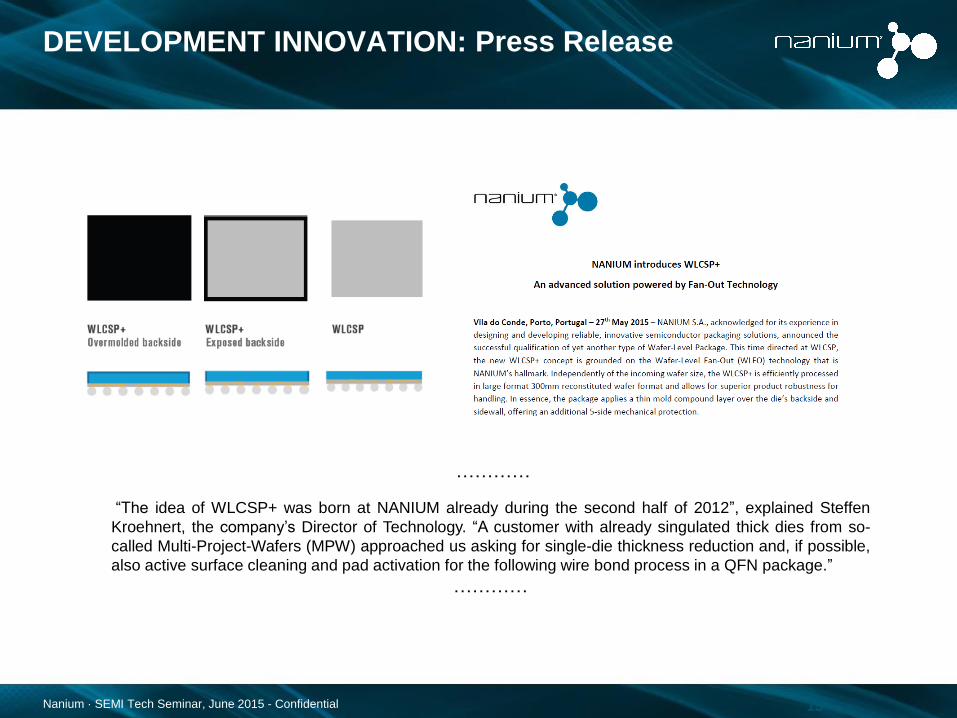
DEVELOPMENT INNOVATION: Press Release
13
…………
“The idea of WLCSP+ was born at NANIUM already during the second half of 2012”, explained Steffen
Kroehnert, the company’s Director of Technology. “A customer with already singulated thick dies from so-
called Multi-Project-Wafers (MPW) approached us asking for single-die thickness reduction and, if possible,
also active surface cleaning and pad activation for the following wire bond process in a QFN package.”
…………

Nanium · SEMI Tech Seminar, June 2015 - Confidential
MEDICAL MARKET: Press Release
14
…………
“The ultra-compact, pocket-sized, Sonic Window is unlike any portable ultrasound device
available on the market today,” said Jim Green, Analogic’s president and chief executive
officer. “We are addressing an unmet need to bring clinicians better vascular access and
care to challenging patients in their practices. Integrating all this processing capacity in such
an extremely small space was a critical requirement. We were impressed with NANIUM’s
capabilities in core areas such as package research, development, test and manufacture.”
………..

Nanium · SEMI Tech Seminar, June 2015 - Confidential 15
…………
““We are investing significant resources and effort to advance our flagship packaging technology,” said
Armando Tavares, president and CEO of NANIUM. “Achieving this higher reliability level gives eWLB
technology access to new applications and markets, presenting us with a wide range of opportunities.”
………..
DEVELOPMENT INNOVATION: Press Release

Nanium · SEMI Tech Seminar, June 2015 - Confidential
Full 12”/300mm production capabilities
16
Wafer-level services
including Wafer-
Prep, Recon,
Lithography, Solder
Ball Attach and
Wafer Test.
Our package offer
includes
WLCSP, WLFO,
WLSiP and WL3D.

Nanium · SEMI Tech Seminar, June 2015 - Confidential
WLP solutions beyond our customers’
expectations
17
THE WAFER-LEVEL
PACKAGE SOLUTION
PROVIDER

Nanium · SEMI Tech Seminar, June 2015 - Confidential 18
WLCSP WLFO
WL3D WLSiP
WLCSP (WAFER-LEVEL CHIP SCALE PACKAGE)
WLCSP enable low-cost Manufacturing of
small die sizes, with low I/O density and high
performance. They cover a wide range of die
sizes, bump height and pitch and Si-die
thickness
Our offer includes WLCSP+, an application of
WLFO Technology know-how to WLCSP that
provides additional edge protection
WLP solutions beyond our customers’
expectations

Nanium · SEMI Tech Seminar, June 2015 - Confidential 19
WLCSP WLFO
WL3D WLSiP
WLFO (WAFER-LEVEL FAN-OUT)
> 550 MILLION UNITS SHIPPED
WLFO allows for system integration on
wafer-level with the highest integration
density, while also ensuring top
performance.
WLP solutions beyond our customers’
expectations

Nanium · SEMI Tech Seminar, June 2015 - Confidential 20
WLCSP
WL3D WLSiP
WLSIP (WAFER-LEVEL SYSTEM-IN-PACKAGE)
Our embedded integration solutions
include Multi-Chip Modules with or
without passives integration.
WLFO
Relevant markets for WLSiP
include Wearables and IoT
WLP solutions beyond our customers’
expectations

Nanium · SEMI Tech Seminar, June 2015 - Confidential 21
WLCSP
WL3D WLSiP
WL3D (WAFER-LEVEL 3D INTEGRATION)
Cutting-edge package solutions that
integrate several packages into a single one.
Includes Wafer-Level Package-on-Package
and Face-to-Face (F2F) package assembly
WLFO
Relevant markets for WL3D
include Wearables and IoT
WLP solutions beyond our customers’
expectations