CDP1802A, CDP1802AC, CDP1802BC - RCA CDP1802 … · •8-Bit Parallel Organization With...
27
3-3 Features • Maximum Input Clock Maximum Frequency Options At V DD = 5V - CDP1802A, AC . . . . . . . . . . . . . . . . . . . . . . . . . 3.2MHz - CDP1802BC. . . . . . . . . . . . . . . . . . . . . . . . . . . . 5.0MHz • Maximum Input Clock Maximum Frequency Options At V DD = 10V - CDP1802A, AC . . . . . . . . . . . . . . . . . . . . . . . . . 6.4MHz • Minimum Instruction Fetch-Execute Times At V DD = 5V - CDP1802A, AC . . . . . . . . . . . . . . . . . . . . . . . . . . 5.0μs - CDP1802BC. . . . . . . . . . . . . . . . . . . . . . . . . . . . . 3.2μs • Any Combination of Standard RAM and ROM Up to 65,536 Bytes •8-Bit Parallel Organization With Bidirectional Data Bus and Multiplexed Address Bus • 16 x 16 Matrix of Registers for Use as Multiple Program Counters, Data Pointers, or Data Registers • On-Chip DMA, Interrupt, and Flag Inputs • Programmable Single-Bit Output Port • 91 Easy-to-Use Instructions Description The CDP1802 family of CMOS microprocessors are 8-bit register oriented central processing units (CPUs) designed for use as general purpose computing or control elements in a wide range of stored program systems or products. The CDP1802 types include all of the circuits required for fetching, interpreting, and executing instructions which have been stored in standard types of memories. Extensive input/output (I/O) control features are also provided to facili- tate system design. The 1800 series architecture is designed with emphasis on the total microcomputer system as an integral entity so that systems having maximum flexibility and minimum cost can be realized. The 1800 series CPU also provides a synchro- nous interface to memories and external controllers for I/O devices, and minimizes the cost of interface controllers. Fur- ther, the I/O interface is capable of supporting devices oper- ating in polled, interrupt driven, or direct memory access modes. The CDP1802A and CDP1802AC have a maximum input clock frequency of 3.2MHz at V DD = 5V. The CDP1802A and CDP1802AC are functionally identical. They differ in that the CDP1802A has a recommended operating voltage range of 4V to 10.5V, and the CDP1802AC a recommended operat- ing voltage range of 4V to 6.5V. The CDP1802BC is a higher speed version of the CDP1802AC, having a maximum input clock frequency of 5.0MHz at V DD = 5V, and a recommended operating voltage range of 4V to 6.5V. Ordering Information PART NUMBER TEMPERATURE RANGE PACKAGE PKG. NO. 5V - 3.2MHz 5V - 5MHz CDP1802ACE CDP1802BCE -40 o C to +85 o C PDIP E40.6 CDP1802ACEX CDP1802BCEX Burn-In E40.6 CDP1802ACQ CDP1802BCQ -40 o C to +85 o C PLCC N44.65 CDP1802ACD - -40 o C to +85 o C SBDIP D40.6 CDP1802ACDX CDP1802BCDX Burn-In D40.6 March 1997 File Number 1305.2 CDP1802A, CDP1802AC, CDP1802BC CMOS 8-Bit Microprocessors CAUTION: These devices are sensitive to electrostatic discharge; follow proper IC Handling Procedures. http://www.intersil.com or 407-727-9207 | Copyright © Intersil Corporation 1999 [ /Title (CDP1 802A, CDP18 02AC, CDP18 02BC) /Sub- ject (CMO S 8- Bit Micro- proces- sors) /Autho r () /Key- words (Inter- sil Corpo- ration, 8-bit micro- proces- sors, 8 bit micro- proces- sors, periph- erals) /Cre- ator () /DOCI NFO pdf- mark
Transcript of CDP1802A, CDP1802AC, CDP1802BC - RCA CDP1802 … · •8-Bit Parallel Organization With...

3-3
Features• Maximum Input Clock Maximum Frequency Options
At VDD = 5V- CDP1802A, AC . . . . . . . . . . . . . . . . . . . . . . . . . 3.2MHz- CDP1802BC. . . . . . . . . . . . . . . . . . . . . . . . . . . . 5.0MHz
• Maximum Input Clock Maximum Frequency OptionsAt VDD = 10V- CDP1802A, AC . . . . . . . . . . . . . . . . . . . . . . . . . 6.4MHz
• Minimum Instruction Fetch-Execute TimesAt VDD = 5V- CDP1802A, AC . . . . . . . . . . . . . . . . . . . . . . . . . . 5.0µs- CDP1802BC. . . . . . . . . . . . . . . . . . . . . . . . . . . . . 3.2µs
• Any Combination of Standard RAM and ROM Up to65,536 Bytes
• 8-Bit Parallel Organization With Bidirectional Data Busand Multiplexed Address Bus
• 16 x 16 Matrix of Registers for Use as MultipleProgram Counters, Data Pointers, or Data Registers
• On-Chip DMA, Interrupt, and Flag Inputs
• Programmable Single-Bit Output Port
• 91 Easy-to-Use Instructions
DescriptionThe CDP1802 family of CMOS microprocessors are 8-bitregister oriented central processing units (CPUs) designedfor use as general purpose computing or control elements ina wide range of stored program systems or products.
The CDP1802 types include all of the circuits required forfetching, interpreting, and executing instructions which havebeen stored in standard types of memories. Extensiveinput/output (I/O) control features are also provided to facili-tate system design.
The 1800 series architecture is designed with emphasis onthe total microcomputer system as an integral entity so thatsystems having maximum flexibility and minimum cost canbe realized. The 1800 series CPU also provides a synchro-nous interface to memories and external controllers for I/Odevices, and minimizes the cost of interface controllers. Fur-ther, the I/O interface is capable of supporting devices oper-ating in polled, interrupt driven, or direct memory accessmodes.
The CDP1802A and CDP1802AC have a maximum inputclock frequency of 3.2MHz at VDD = 5V. The CDP1802A andCDP1802AC are functionally identical. They differ in that theCDP1802A has a recommended operating voltage range of4V to 10.5V, and the CDP1802AC a recommended operat-ing voltage range of 4V to 6.5V.
The CDP1802BC is a higher speed version of theCDP1802AC, having a maximum input clock frequency of5.0MHz at VDD = 5V, and a recommended operating voltagerange of 4V to 6.5V.
Ordering InformationPART NUMBER
TEMPERATURE RANGE PACKAGE PKG. NO.5V - 3.2MHz 5V - 5MHz
CDP1802ACE CDP1802BCE -40oC to +85oC PDIP E40.6
CDP1802ACEX CDP1802BCEX Burn-In E40.6
CDP1802ACQ CDP1802BCQ -40oC to +85oC PLCC N44.65
CDP1802ACD - -40oC to +85oC SBDIP D40.6
CDP1802ACDX CDP1802BCDX Burn-In D40.6
March 1997
File Number 1305.2
CDP1802A, CDP1802AC,CDP1802BC
CMOS 8-Bit Microprocessors
CAUTION: These devices are sensitive to electrostatic discharge; follow proper IC Handling Procedures.http://www.intersil.com or 407-727-9207 | Copyright © Intersil Corporation 1999
[ /Title(CDP1802A,CDP1802AC,CDP1802BC)/Sub-ject(CMOS 8-BitMicro-proces-sors)/Author ()/Key-words(Inter-silCorpo-ration,8-bitmicro-proces-sors, 8bitmicro-proces-sors,periph-erals)/Cre-ator ()/DOCINFOpdf-mark
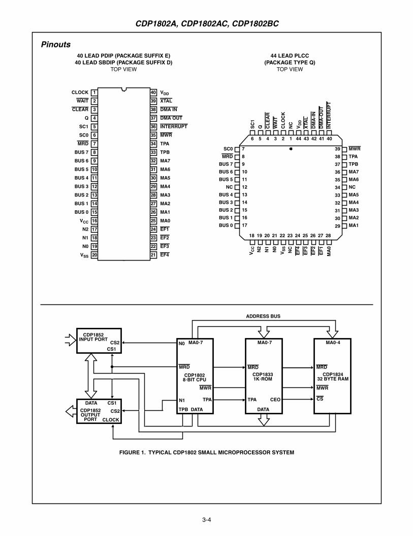
3-4
Pinouts40 LEAD PDIP (PACKAGE SUFFIX E)
40 LEAD SBDIP (PACKAGE SUFFIX D)TOP VIEW
44 LEAD PLCC(PACKAGE TYPE Q)
TOP VIEW
FIGURE 1. TYPICAL CDP1802 SMALL MICROPROCESSOR SYSTEM
13
1
2
3
4
5
6
7
8
9
10
11
12
14
15
16
17
18
19
20
CLOCK
WAIT
CLEAR
Q
SC1
SC0
MRD
BUS 7
BUS 6
BUS 5
BUS 4
BUS 3
BUS 2
BUS 1
BUS 0
VCC
N2
N1
N0
VSS
28
40
39
38
37
36
35
34
33
32
31
30
29
27
26
25
24
23
22
21
VDD
XTAL
DMA IN
DMA OUT
INTERRUPT
MWR
TPA
TPB
MA7
MA6
MA5
MA4
MA3
MA2
MA1
MA0
EF1
EF2
EF3
EF4
44 43 42 41 40
3938373635343332313029
2827
123456
262524232221201918
7891011121314151617
SC0MRD
BUS 7BUS 6BUS 5
NCBUS 4BUS 3BUS 2BUS 1BUS 0
SC1
Q CLE
AR
WA
ITC
LOC
KN
CV D
DXT
AL
DM
A-IN
DM
A-O
UT
INTE
RRU
PT
V CC N2
N1
N0
V SS
NC
EF4
EF3
EF2
EF1
MA
0
MWRTPATPBMA7MA6NCMA5MA4MA3MA2MA1
CDP1852INPUT PORT
DATA CS1CS2CDP1852
OUTPUTPORT CLOCK
CS1CS2 MA0-7N0
MRD
MWR
N1
TPB DATA
TPA
CDP18028-BIT CPU
MRD
MA0-4
MWR
CS
CDP182432 BYTE RAM
MA0-7
DATA
CDP18331K-ROM
CEOTPA
MRD
ADDRESS BUS
CDP1802A, CDP1802AC, CDP1802BC

3-5
Block Diagram
FIGURE 2.
MUX
MA7 MA5 MA3 MA1MA0MA2MA4MA6
MEMORY ADDRESS LINES I/O FLAGS
ALUB
D
DFINCR/DECR
A
R(0).1 R(0).0R(1).0R(1).1
R(2).1 R(2).0
R(9).0R(A).0R(A).1
R(9).1
R(E).1R(F).1 R(F).0
R(E).0
REGISTERARRAY
8-BIT BIDIRECTIONAL DATA BUS
LATCHAND
DECODE
R
X T P I N N1
N0
N2
I/OCOMMANDS
BUS 0
BUS 1
BUS 2
BUS 3
BUS 4
BUS 5
BUS 6
BUS 7
TO INSTRUCTIONDECODE
CONTROL ANDTIMING LOGIC
CLOCKLOGIC
I/O REQUESTS
CONTROL
EF1 EF3EF2 EF4
DMAOUT
DMAIN INT
CLEARWAIT
CLOCK
XTALSCOSCIQ LOGICTPATPBMWRMRD
SYSTEM
STATECODES
TIMING
CDP1802A, CDP1802AC, CDP1802BC
3-6
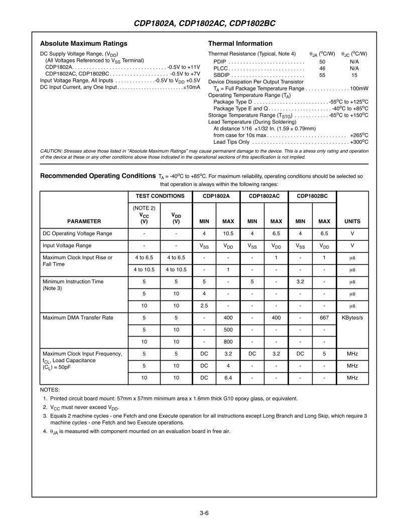
Absolute Maximum Ratings Thermal InformationDC Supply Voltage Range, (VDD)
(All Voltages Referenced to VSS Terminal)CDP1802A. . . . . . . . . . . . . . . . . . . . . . . . . . . . . . . . . -0.5V to +11VCDP1802AC, CDP1802BC. . . . . . . . . . . . . . . . . . . . -0.5V to +7V
Input Voltage Range, All Inputs . . . . . . . . . . . . . .-0.5V to VDD +0.5VDC Input Current, any One Input . . . . . . . . . . . . . . . . . . . . . . . . .±10mA
Thermal Resistance (Typical, Note 4) θJA (oC/W) θJC (oC/W)PDIP . . . . . . . . . . . . . . . . . . . . . . . . . . 50 N/APLCC . . . . . . . . . . . . . . . . . . . . . . . . . . 46 N/ASBDIP . . . . . . . . . . . . . . . . . . . . . . . . . 55 15
Device Dissipation Per Output TransistorTA = Full Package Temperature Range . . . . . . . . . . . . . . . 100mW
Operating Temperature Range (TA)Package Type D . . . . . . . . . . . . . . . . . . . . . . . . . . -55oC to +125oCPackage Type E and Q . . . . . . . . . . . . . . . . . . . . . . -40oC to +85oC
Storage Temperature Range (TSTG) . . . . . . . . . . . . -65oC to +150oCLead Temperature (During Soldering)
At distance 1/16 ±1/32 In. (1.59 ± 0.79mm)from case for 10s max . . . . . . . . . . . . . . . . . . . . . . . . . . . +265oCLead Tips Only . . . . . . . . . . . . . . . . . . . . . . . . . . . . . . . . . +300oC
CAUTION: Stresses above those listed in “Absolute Maximum Ratings” may cause permanent damage to the device. This is a stress only rating and operationof the device at these or any other conditions above those indicated in the operational sections of this specification is not implied.
Recommended Operating Conditions TA = -40oC to +85oC. For maximum reliability, operating conditions should be selected sothat operation is always within the following ranges:
PARAMETER
TEST CONDITIONS CDP1802A CDP1802AC CDP1802BC
UNITS
(NOTE 2)VCC(V)
VDD(V) MIN MAX MIN MAX MIN MAX
DC Operating Voltage Range - - 4 10.5 4 6.5 4 6.5 V
Input Voltage Range - - VSS VDD VSS VDD VSS VDD V
Maximum Clock Input Rise orFall Time
4 to 6.5 4 to 6.5 - - - 1 - 1 µs
4 to 10.5 4 to 10.5 - 1 - - - - µs
Minimum Instruction Time(Note 3)
5 5 5 - 5 - 3.2 - µs
5 10 4 - - - - - µs
10 10 2.5 - - - - - µs
Maximum DMA Transfer Rate 5 5 - 400 - 400 - 667 KBytes/s
5 10 - 500 - - - -
10 10 - 800 - - - -
Maximum Clock Input Frequency,fCL, Load Capacitance(CL) = 50pF
5 5 DC 3.2 DC 3.2 DC 5 MHz
5 10 DC 4 - - - - MHz
10 10 DC 6.4 - - - - MHz
NOTES:1. Printed circuit board mount: 57mm x 57mm minimum area x 1.6mm thick G10 epoxy glass, or equivalent.2. VCC must never exceed VDD.3. Equals 2 machine cycles - one Fetch and one Execute operation for all instructions except Long Branch and Long Skip, which require 3
machine cycles - one Fetch and two Execute operations.4. θJA is measured with component mounted on an evaluation board in free air.
CDP1802A, CDP1802AC, CDP1802BC

3-7
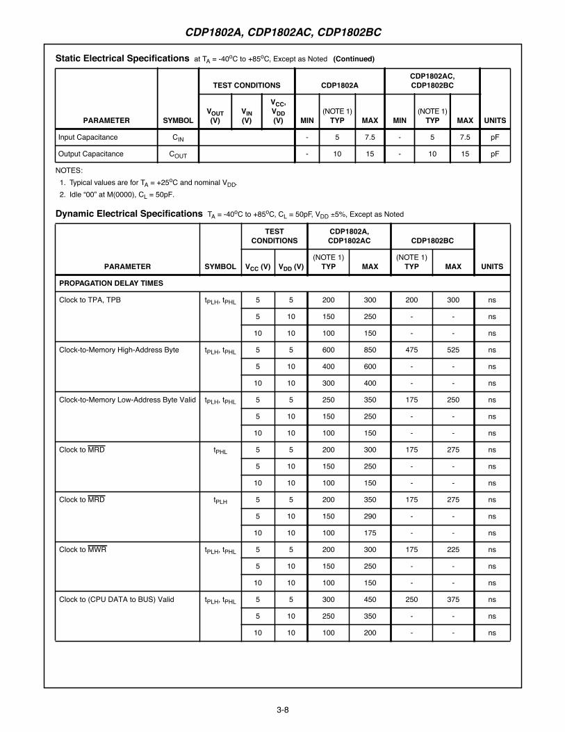
Static Electrical Specifications at TA = -40oC to +85oC, Except as Noted
PARAMETER SYMBOL
TEST CONDITIONS CDP1802ACDP1802AC,CDP1802BC
UNITSVOUT(V)
VIN(V)
VCC,VDD(V) MIN
(NOTE 1)TYP MAX MIN
(NOTE 1)TYP MAX
Quiescent Device Current IDD - - 5 - 0.1 50 - 1 200 µA
- - 10 - 1 200 - - - µA
Output Low Drive (Sink)Current IOL 0.4 0, 5 5 1.1 2.2 - 1.1 2.2 - mA
(Except XTAL) 0.5 0, 10 10 2.2 4.4 - - - - mA
XTAL 0.4 5 5 170 350 - 170 350 - µA
Output High Drive (Source)Current IOH 4.6 0, 5 5 -0.27 -0.55 - -0.27 -0.55 - mA
(Except XTAL) 9.5 0, 10 10 -0.55 -1.1 - - - - mA
XTAL 4.6 0 5 -125 -250 - -125 -250 - µA
Output Voltage - 0, 5 5 - 0 0.1 - 0 0.1 VLow Level VOL - 0, 10 10 - 0 0.1 - - - V
Output Voltage - 0, 5 5 4.9 5 - 4.9 5 - VHigh Level VOH - 0, 10 10 9.9 10 - - - - V
Input Low Voltage VIL 0.5, 4.5 - 5 - - 1.5 - - 1.5 V
0.5, 4.5 - 5, 10 - - 1 - - - V
1, 9 - 10 - - 3 - - - V
Input High Voltage VIH 0.5, 4.5 - 5 3.5 - - 3.5 - - V
0.5, 4.5 - 5, 10 4 - - - - - V
1, 9 - 10 7 - - - - - V
CLEAR Input Voltage VH - - 5 0.4 0.5 - 0.4 0.5 - V
Schmitt Hysteresis - - 5, 10 0.3 0.4 - - - - V
- - 10 1.5 2 - - - - V
Input Leakage Current IIN AnyInput
0, 5 5 - ±10-4 ±1 - ±10-4 ±1 µA
0, 10 10 - ±10-4 ±1 - - - µA
Three-State Output Leakage IOUT 0, 5 0, 5 5 - ±10-4 ±1 - ±10-4 ±1 µA
Current 0, 10 0, 10 10 - ±10-4 ±1 - - - µA
Operating CurrentCDP1802A, ACat f = 3.2MHz
IDDI(Note 2)
- - 5 - 2 4 - 2 4 mA
CDP1802BCat f = 5.0MHz
- - 5 - - - - 3 6 mA
Minimum Data RetentionVoltage
VDR VDD = VDR - 2 2.4 - 2 2.4 V
Data Retention Current IDR VDD = 2.4V - 0.05 - - 0.5 - µA
CDP1802A, CDP1802AC, CDP1802BC
3-8
Input Capacitance CIN - 5 7.5 - 5 7.5 pF
Output Capacitance COUT - 10 15 - 10 15 pF
NOTES:1. Typical values are for TA = +25oC and nominal VDD.2. Idle “00” at M(0000), CL = 50pF.
Dynamic Electrical Specifications TA = -40oC to +85oC, CL = 50pF, VDD ±5%, Except as Noted
PARAMETER SYMBOL
TESTCONDITIONS
CDP1802A,CDP1802AC CDP1802BC
UNITSVCC (V) VDD (V)(NOTE 1)
TYP MAX(NOTE 1)
TYP MAX
PROPAGATION DELAY TIMES
Clock to TPA, TPB tPLH, tPHL 5 5 200 300 200 300 ns
5 10 150 250 - - ns
10 10 100 150 - - ns
Clock-to-Memory High-Address Byte tPLH, tPHL 5 5 600 850 475 525 ns
5 10 400 600 - - ns
10 10 300 400 - - ns
Clock-to-Memory Low-Address Byte Valid tPLH, tPHL 5 5 250 350 175 250 ns
5 10 150 250 - - ns
10 10 100 150 - - ns
Clock to MRD tPHL 5 5 200 300 175 275 ns
5 10 150 250 - - ns
10 10 100 150 - - ns
Clock to MRD tPLH 5 5 200 350 175 275 ns
5 10 150 290 - - ns
10 10 100 175 - - ns
Clock to MWR tPLH, tPHL 5 5 200 300 175 225 ns
5 10 150 250 - - ns
10 10 100 150 - - ns
Clock to (CPU DATA to BUS) Valid tPLH, tPHL 5 5 300 450 250 375 ns
5 10 250 350 - - ns
10 10 100 200 - - ns
Static Electrical Specifications at TA = -40oC to +85oC, Except as Noted (Continued)
PARAMETER SYMBOL
TEST CONDITIONS CDP1802ACDP1802AC,CDP1802BC
UNITSVOUT(V)
VIN(V)
VCC,VDD(V) MIN
(NOTE 1)TYP MAX MIN
(NOTE 1)TYP MAX
CDP1802A, CDP1802AC, CDP1802BC

3-9
Clock to State Code tPLH, tPHL 5 5 300 450 250 400 ns
5 10 250 350 - - ns
10 10 150 250 - - ns
Clock to Q tPLH, tPHL 5 5 250 400 200 300 ns
5 10 150 250 - - ns
10 10 100 150 - - ns
Clock to N (0 - 2) tPLH, tPHL 5 5 300 550 275 350 ns
5 10 200 350 - - ns
10 10 150 250 - - ns
MINIMUM SET UP AND HOLD TIMES
Data Bus Input Set Up tSU 5 5 -20 25 -20 0 ns
5 10 0 50 - - ns
10 10 -10 40 - - ns
Data Bus Input Hold tH(Note 2)
5 5 150 200 125 150 ns
5 10 100 125 - - ns
10 10 75 100 - - ns
DMA Set Up tSU 5 5 0 30 0 30 ns
5 10 0 20 - - ns
10 10 0 10 - - ns
DMA Hold tH(Note 2)
5 5 150 250 100 150 ns
5 10 100 200 - - ns
10 10 75 125 - - ns
Interrupt Set Up tSU 5 5 -75 0 -75 0 ns
5 10 -50 0 - - ns
10 10 -25 0 - - ns
Interrupt Hold tH(Note 2)
5 5 100 150 75 125 ns
5 10 75 100 - - ns
10 10 50 75 - - ns
WAIT Set Up tSU 5 5 10 50 20 40 ns
5 10 -10 15 - - ns
10 10 0 25 - - ns
Dynamic Electrical Specifications TA = -40oC to +85oC, CL = 50pF, VDD ±5%, Except as Noted (Continued)
PARAMETER SYMBOL
TESTCONDITIONS
CDP1802A,CDP1802AC CDP1802BC
UNITSVCC (V) VDD (V)(NOTE 1)
TYP MAX(NOTE 1)
TYP MAX
CDP1802A, CDP1802AC, CDP1802BC

3-10
EF1-4 Set Up tSU 5 5 -30 20 -30 0 ns
5 10 -20 30 - - ns
10 10 -10 40 - - ns
EF1-4 Hold tH(Note 2)
5 5 150 200 100 150 ns
5 10 100 150 - - ns
10 10 75 100 - - ns
Minimum Pulse Width TimesCLEAR Pulse Width tWL
(Note 2)5 5 150 300 100 150 ns
5 10 100 200 - - ns
10 10 75 150 - - ns
CLOCK Pulse Width tWL 5 5 125 150 90 100 ns
5 10 100 125 - - ns
10 10 60 75 - - ns
NOTES:1. Typical values are for TA = +25oC and nominal VDD.2. Maximum limits of minimum characteristics are the values above which all devices function.
Timing Specifications as a function of T(T = 1/fCLOCK) at TA = -40 to +85oC, Except as Noted
PARAMETERS SYMBOL
TEST CONDITIONSCDP1802A,CDP1802AC CDP1802BC
UNITSVCC (V) VDD (V) MIN(NOTE 1)
TYP MIN(NOTE 1)
TYP
High-Order Memory-Address ByteSet Up to TPA Time
tSU 5 5 2T-550 2T-400 2T-325 2T-275 ns
5 10 2T-350 2T250 - - ns
10 10 2T-250 2T-200 - - ns
High-Order Memory-Address ByteHold After TPA Time
tH 5 5 t/2-25 T/2-15 T/2-25 T/2-15 ns
5 10 T/2-35 T/2-25 - - ns
10 10 T/2-10 T/2-+0 - - ns
Low-Order Memory-Address ByteHold After WR Time
tH 5 5 T-30 T+0 T-30 T+0 ns
5 10 T-20 T+0 - - ns
10 10 T-10 T+0 - - ns
CPU Data to Bus Hold After WRTime
tH 5 5 T-200 T-150 T-175 T-125 ns
5 10 T-150 T-100 - - ns
10 10 T-100 T-50 - - ns
Dynamic Electrical Specifications TA = -40oC to +85oC, CL = 50pF, VDD ±5%, Except as Noted (Continued)
PARAMETER SYMBOL
TESTCONDITIONS
CDP1802A,CDP1802AC CDP1802BC
UNITSVCC (V) VDD (V)(NOTE 1)
TYP MAX(NOTE 1)
TYP MAX
CDP1802A, CDP1802AC, CDP1802BC

3-11
Required Memory Access TimeAddress to Data
tACC 5 5 5T-375 5T-250 5T-225 5T-175 ns
5 10 5T-250 5T-150 - - ns
10 10 5T-190 5T-100 - - ns
MRD to TPA tSU 5 5 T/2-25 T/2-18 T/2-20 T/2-15 ns
5 10 T/2-20 T/2-15 - - ns
10 10 T/2-15 T/2-10 - - ns
NOTE:1. Typical values are for TA = +25oC and nominal VDD.
Timing Specifications as a function of T(T = 1/fCLOCK) at TA = -40 to +85oC, Except as Noted
PARAMETERS SYMBOL
TEST CONDITIONSCDP1802A,CDP1802AC CDP1802BC
UNITSVCC (V) VDD (V) MIN(NOTE 1)
TYP MIN(NOTE 1)
TYP
Timing Waveforms
FIGURE 3. BASIC DC TIMING WAVEFORM, ONE INSTRUCTION CYCLE
FETCH (READ) EXECUTE (WRITE)
00 01 10 11 20 21 30 31 40 41 50 51 60 61 70 71 00 01 10 11 20 21 30 31 40 41 50 51 60 61 70 71 00
HI BYTE LOW BYTEHI BYTE LOW BYTE
CLOCK
ADDRESS
TPA
TPB
MRD
MWR
DATA VALID INPUT DATA VALID OUTPUT DATA
CDP1802A, CDP1802AC, CDP1802BC

3-12
NOTES:1. This timing diagram is used to show signal relationships only and does not represent any specific machine cycle.2. All measurements are referenced to 50% point of the waveforms.3. Shaded areas indicate “Don’t Care” or undefined state. Multiple transitions may occur during this period.
FIGURE 4. TIMING WAVEFORM
Timing Waveforms (Continued)
CLOCK
TPA
TPB
MEMORY
MRD
MWR
(I/O EXECUTION
Q
DATA FROM
DMA
INTERRUPT
EF 1-4
WAIT
CLEAR
REQUEST
REQUEST
BUS TO CPU
N0, N1, N2
STATE
DATA FROMCPU TO BUS
(MEMORYWRITE CYCLE)
(MEMORY
ADDRESS
READ CYCLE)
CODES
CYCLE)
tW
00 10 20 30 40 50 60 70 0001 11 21 31 41 51 61 71 01
0 1 2 3 4 5 6 7 0
tPLH tPHL
tPLH tPHL
tPLH, tPHL
tSU
DMA SAMPLED (S1, S2, S3)
tH
ADDRESS BYTEHIGH ORDER
tPHLtPLH tSU
tPLH, tPHL tPLH, tPHL
tPLH
tH
tPLH
tH
tPLH, tPHL
tPLH, tPHL
tPLH, tPHL
ADDRESS BYTELOW ORDER
tPHLtPLHtPHL
tPLH
tPHL
tPLH
tPLH
DATALATCHED IN CPU
tSU tH
tSU tH
tSU tH
INTERRUPTSAMPLED (S1, S2)
FLAG LINESSAMPLED (IN S1)
ANY NEGATIVETRANSITION
tSU
tW
tSU tH
CDP1802A, CDP1802AC, CDP1802BC

3-13
Machine Cycle Timing Waveforms (Propagation Delays Not Shown)
FIGURE 5. GENERAL TIMING WAVEFORMS
FIGURE 6. NON-MEMORY CYCLE TIMING WAVEFORMS
FIGURE 7. MEMORY WRITE CYCLE TIMING WAVEFORMS
CLOCK
TPA
TPB
MACHINE
MA
CYCLE
0 1 2 3 4 5 6 7 0 1 2 3 4 5 6 7 0 1 2 3 4 5 6 7 0
CYCLE n CYCLE (n + 1) CYCLE (n + 2)
LOW ADDRESSHIGH ADDLOW ADDRESSHIGH ADDLOW ADDRESSHIGH ADD
MEMORY READ CYCLENON MEMORY CYCLEMEMORY READ CYCLE
INSTRUCTION
MRD
MWR (HIGH)
MEMORYOUTPUT
FETCH (S0) EXECUTE (S1) FETCH (S0) EXECUTE
ALLOWABLE MEMORY ACCESS VALID OUTPUT VALIDOUTPUT
“DON’T CARE” OR INTERNAL DELAYS HIGH IMPEDANCE STATE
MEMORYOUTPUT
ALLOWABLE MEMORY ACCESS VALID OUTPUT VALIDOUTPUT
MEMORY READ CYCLEMEMORY WRITE CYCLEMEMORY READ CYCLE
INSTRUCTION FETCH (S0) EXECUTE (S1) FETCH (S0) EXECUTE
CPU OUTPUT OFF VALID DATA OFF VALID
MWR
MRD
TO MEMORY
“DON’T CARE” OR INTERNAL DELAYS HIGH IMPEDANCE STATE
CDP1802A, CDP1802AC, CDP1802BC

3-14
FIGURE 8. MEMORY READ CYCLE TIMING WAVEFORMS
FIGURE 9. LONG BRANCH OR LONG SKIP CYCLE TIMING WAVEFORMS
Machine Cycle Timing Waveforms (Propagation Delays Not Shown) (Continued)
MEMORY READ CYCLEMEMORY READ CYCLEMEMORY READ CYCLE
INSTRUCTION FETCH (S0) EXECUTE (S1) FETCH (S0) EXECUTE
MEMORYOUTPUT
ALLOWABLE MEMORY ACCESS VALID OUTPUT VALIDOUTPUT
MRD
MWR (HIGH)
“DON’T CARE” OR INTERNAL DELAYS HIGH IMPEDANCE STATE
VALIDOUTPUT
MEMORYOUTPUT
ALLOWABLE MEMORY ACCESS VALID OUTPUT VALIDOUTPUT
MEMORY READ CYCLEMEMORY READ CYCLEMEMORY READ CYCLE
INSTRUCTION FETCH (S0) EXECUTE (S1) EXECUTE (S1) FETCH (S0)
MRD
MWR (HIGH)
“DON’T CARE” OR INTERNAL DELAYS HIGH IMPEDANCE STATE
VALID OUTPUT
CDP1802A, CDP1802AC, CDP1802BC

3-15
FIGURE 10. INPUT CYCLE TIMING WAVEFORMS
FIGURE 11. OUTPUT CYCLE TIMING WAVEFORMS
Machine Cycle Timing Waveforms (Propagation Delays Not Shown) (Continued)
CLOCK0 1 2 3 4 5 6 7 0 1 2 3 4 5 6 7
MEMORYOUTPUT
ALLOWABLE MEMORY ACCESS VALID OUTPUT
TPA
TPB
MACHINE
INSTRUCTION
MRD
N0 - N2
DATA
MWR
CYCLE
BUS
MEMORY READ CYCLE MEMORY WRITE CYCLE
VALID DATA FROM INPUT DEVICE
N = 9 - F
EXECUTE (S1)
CYCLE (n + 1)CYCLE n
FETCH (S0)
NOTE 1“DON’T CARE” OR INTERNAL DELAYS HIGH IMPEDANCE STATE
(NOTE 1)
USER GENERATED SIGNAL
0
CLOCK0 1 2 3 4 5 6 7 0 1 2 3 4 5 6 7
TPA
TPB
MACHINE
INSTRUCTION
CYCLE
EXECUTE (S1)
CYCLE (n + 1)CYCLE n
FETCH (S0)
DATA BUS
ALLOWABLE MEMORY ACCESS VALID OUTPUTVALID DATA FROM MEMORY
ALLOWABLE MEMORY ACCESS
MEMORY READ CYCLEMEMORY READ CYCLE
MRD
N0 - N2
DATA STROBE(MRD • TPB • N)
NOTE 1“DON’T CARE” OR INTERNAL DELAYS HIGH IMPEDANCE STATE
(NOTE 1)
USER GENERATED SIGNAL
0
N = 1 - 9
CDP1802A, CDP1802AC, CDP1802BC

3-16
FIGURE 12. DMA IN CYCLE TIMING WAVEFORMS
FIGURE 13. DMA OUT CYCLE TIMING WAVEFORMS
Machine Cycle Timing Waveforms (Propagation Delays Not Shown) (Continued)
CLOCK0 1 2 3 4 5 6 7 0 1 2 3 4 5 6 7 0 1 2 3
TPA
TPBMACHINE
INSTRUCTION
DMA-IN
MRD
MWR
MEMORY
DATA BUS
CYCLE
OUTPUT
4 5 6 7
NOTE 1
MEMORY READ CYCLE MEMORY READ, WRITE MEMORY WRITE CYCLEOR NON-MEMORY CYCLE
“DON’T CARE” OR INTERNAL DELAYS HIGH IMPEDANCE STATE
(NOTE 1)
USER GENERATED SIGNAL
VALID DATA FROM INPUT DEVICE
CYCLE n
FETCH (S0)
CYCLE (n+1)
EXECUTE (S1)
CYCLE (n+2)
DMA (S2)
VALID OUTPUT
0 1 2 3 4 5 6 7 0 1 2 3 4 5 6 7 0 1 2 3 4 5 6
CLOCK
TPA
TPB
MACHINECYCLE
INSTRUCTION
DMA OUT
MRD
MWR
MEMORYOUTPUT
DATASTROBE
(S2 • TPB)
CYCLE n CYCLE (n + 1) CYCLE (n + 2)
DMA (S2)EXECUTE (S1)FETCH (S0)
VALID OUTPUT VALID DATA FROM MEMORY
NOTE 1
MEMORY READ CYCLE MEMORY READ, WRITE MEMORY READ CYCLEOR NON-MEMORY CYCLE
“DON’T CARE” OR INTERNAL DELAYS HIGH IMPEDANCE STATEUSER GENERATED SIGNAL
(NOTE 1)
(NOTE 1)
CDP1802A, CDP1802AC, CDP1802BC

3-17
FIGURE 14. INTERRUPT CYCLE TIMING WAVEFORMS
Performance Curves
FIGURE 15. CDP1802A, AC TYPICAL MAXIMUM CLOCKFREQUENCY AS A FUNCTION OF TEMPERATURE
FIGURE 16. CDP1802BC TYPICAL MAXIMUM CLOCKFREQUENCY AS A FUNCTION OF TEMPERATURE
Machine Cycle Timing Waveforms (Propagation Delays Not Shown) (Continued)
0 1 2 3 4 5 6 7 0 1 2 3 4 5 6 7 0 1 2 3 4 5 6
CLOCK
TPA
TPB
MACHINECYCLE
INSTRUCTION
CYCLE n CYCLE (n + 1) CYCLE (n + 2)
INTERRUPT (S3)EXECUTE (S1)FETCH (S0)
MRD
MWR
INTERRUPT
MEMORYOUTPUT
VALID OUTPUT
NOTE 1
MEMORY READ CYCLE MEMORY READ, WRITE NON-MEMORY CYCLEOR NON-MEMORY CYCLE
“DON’T CARE” OR INTERNAL DELAYS HIGH IMPEDANCE STATE
(NOTE 1)
(INTERNAL) IE
USER GENERATED SIGNAL
8
7
6
5
4
3
2
1
025 35 45 55 65 75 85 95 105 115 125
f CL,
SYS
TEM
MA
XIM
UM
CLO
CK
FREQ
UEN
CY
(MH
z)
TA, AMBIENT TEMPERATURE (oC)
CL, LOAD CAPACITANCE = 50pF
VCC = VDD = 10V
VCC = 5V, VDD = 10V
VCC = VDD = 5V
CL, LOAD CAPACITANCE = 50pF
VCC = VDD = 5V
8
7
6
5
4
3
2
1
025 35 45 55 65 75 85 95 105 115 125
f CL,
SYS
TEM
MA
XIM
UM
CLO
CK
FREQ
UEN
CY
(MH
z)
TA, AMBIENT TEMPERATURE (oC)
CDP1802A, CDP1802AC, CDP1802BC

3-18
FIGURE 17. TYPICAL TRANSITION TIME vs LOAD CAPACI-TANCE FOR ALL TYPES
FIGURE 18. CDP1802A, AC MINIMUM OUTPUT HIGH (SOURCE)CURRENT CHARACTERISTICS
FIGURE 19. CDP1802A, AC MINIMUM OUTPUT LOW (SINK)CURRENT CHARACTERISTICS
FIGURE 20. CDP1802BC MINIMUM OUTPUT HIGH (SOURCE)CURRENT CHARACTERISTICS
FIGURE 21. CDP1802BC MINIMUM OUTPUT LOW (SINK)CURRENT CHARACTERISTICS
FIGURE 22. TYPICAL CHANGE IN PROPAGATION DELAY AS AFUNCTION OF A CHANGE IN LOAD CAPACITANCEFOR ALL TYPES
Performance Curves (Continued)
400
350
300
250
200
150
100
50
00 25 50 75 100 125 150 175 200
t TH
L, t T
LH, T
RA
NSI
TIO
N T
IME
(ns)
CL, LOAD CAPACITANCE (pF)
TA = 25oC
VCC = VDD = 10V
VCC = VDD = 5V
VCC = VDD = 5V
VCC = VDD = 10V
tTLH
tTHL
VGS, GATE-TO-VOLTAGE = -5V
TA, AMBIENT TEMPERATURE = -40oC TO +85oC
-10V
VDS, DRAIN-TO-SOURCE VOLTAGE (V)-10 -9 -8 -7 -6 -5 -4 -3 -2 -1 0
1
2
3
4
5
6
7
I OH
, OU
TPU
T H
IGH
(SO
UR
CE)
CU
RR
ENT
(mA
)
VGS, GATE-TO-SOURCE = 10V
TA = -40oC TO +85oC
5V
VDS, DRAIN-TO-SOURCE VOLTAGE (V)
I OL,
OU
TPU
T LO
W (S
INK
) CU
RR
ENT
(mA
)
0 1 2 3 4 5 6 7 8 9 10
5
10
15
20
25
30
35
VGS, GATE-TO-VOLTAGE = -5V
VDS, DRAIN-TO-SOURCE VOLTAGE (V)-5 -4 -3 -2 -1 0
1
2
3
4 I OH
, OU
TPU
T H
IGH
(SO
UR
CE)
CU
RR
ENT
(mA
)
VGS, GATE-TO-SOURCE = 5V
TA = -40oC TO +85oC
VDS, DRAIN-TO-SOURCE VOLTAGE (V)
I OL,
OU
TPU
T LO
W (S
INK
) CU
RR
ENT
(mA
)
0 1 2 3 4 5
5
10
20
150
125
100
75
50
25
025 50 100 150 200
Δt P
LH,Δ
t PH
L,Δ
PRO
PAG
ATIO
N D
ELAY
TIM
E (n
s)
ΔCL, Δ LOAD CAPACITANCE (pF)
TA = 25oC
VCC = VDD = 10V
VCC = VDD = 5V
VCC = VDD = 5V
VCC = VDD = 10V
ΔtPLH
ΔtPHL
NOTE: ANY OUTPUT EXCEPT XTAL
CDP1802A, CDP1802AC, CDP1802BC

3-19
Signal DescriptionsBus 0 to Bus 7 (Data Bus)
8-bit bidirectional DATA BUS lines. These lines are used fortransferring data between the memory, the microprocessor,and I/O devices.
N0 to N2 (I/O Control Lines)
Activated by an I/O instruction to signal the I/O control logic ofa data transfer between memory and I/O interface. Theselines can be used to issue command codes or device selec-tion codes to the I/O devices (independently or combined withthe memory byte on the data bus when an I/O instruction isbeing executed). The N bits are low at all times except whenan I/O instruction is being executed. During this time theirstate is the same as the corresponding bits in the N register.
The direction of data flow is defined in the I/O instruction by bitN3 (internally) and is indicated by the level of the MRD signal.
MRD = VCC: Data from I/O to CPU and Memory
MRD = VSS: Data from Memory to I/O
EF1 to EF4 (4 Flags)
These inputs enable the I/O controllers to transfer statusinformation to the processor. The levels can be tested by theconditional branch instructions. They can be used in con-junction with the INTERRUPT request line to establish inter-rupt priorities. These flags can also be used by I/O devicesto “call the attention” of the processor, in which case the pro-gram must routinely test the status of these flag(s). Theflag(s) are sampled at the beginning of every S1 cycle.
INTERRUPT, DMA-lN, DMA-OUT (3 I/O Requests)
These inputs are sampled by the CPU during the intervalbetween the leading edge of TPB and the leading edge ofTPA.
Interrupt Action - X and P are stored in T after executingcurrent instruction; designator X is set to 2; designator P isset to 1; interrupt enable is reset to 0 (inhibit); and instructionexecution is resumed. The interrupt action requires onemachine cycle (S3).
DMA Action - Finish executing current instruction; R(0)points to memory area for data transfer; data is loaded intoor read out of memory; and increment R(0).
NOTE: In the event of concurrent DMA and Interrupt requests,DMA-lN has priority followed by DMA-OUT and then Interrupt.
SC0, SC1, (2 State Code Lines)
These outputs indicate that the CPU is: 1) fetching aninstruction, or 2) executing an instruction, or 3) processing aDMA request, or 4) acknowledging an interrupt request. Thelevels of state code are tabulated below. All states are validat TPA. H = VCC, L = VSS.
TPA, TPB (2 Timing Pulses)
Positive pulses that occur once in each machine cycle (TPBfollows TPA). They are used by I/O controllers to interpretcodes and to time interaction with the data bus. The trailingedge of TPA is used by the memory system to latch thehigher-order byte of the 16-bit memory address. TPA is sup-pressed in IDLE when the CPU is in the load mode.
NOTE: IDLE = “00” AT M(0000), BRANCH = “3707” AT M(8107), CL = 50pFFIGURE 23. TYPICAL POWER DISSIPATION AS A FUNCTION OF CLOCK FREQUENCY FOR BRANCH INSTRUCTION AND IDLE
INSTRUCTION FOR ALL TYPES
Performance Curves (Continued)
TA = 25oC
P D, T
YPIC
AL
POW
ER D
ISSI
PATI
ON
FOR
CD
P180
2D (m
W)
fCL, CLOCK INPUT FREQUENCY (MHz)0.01 0.1 1 10
0.1
1
10
100
1000
VCC = VDD = 10V
BRANCH
IDLE
VCC = VDD = 5V
STATE TYPE
STATE CODE LINES
SC1 SC0
S0 (Fetch) L L
S1 (Execute) L H
S2 (DMA) H L
S3 (Interrupt) H H
CDP1802A, CDP1802AC, CDP1802BC

3-20
MA0 to MA7 (8 Memory Address Lines)
In each cycle, the higher-order byte of a 16-bit CPU memoryaddress appears on the memory address lines MA0-7 first.Those bits required by the memory system can be strobedinto external address latches by timing pulse TPA. The loworder byte of the 16-bit address appears on the address linesafter the termination of TPA. Latching of all 8 higher-orderaddress bits would permit a memory system of 64K bytes.
MWR (Write Pulse)
A negative pulse appearing in a memory-write cycle, afterthe address lines have stabilized.
MRD (Read Level)
A low level on MRD indicates a memory read cycle. It can beused to control three-state outputs from the addressed mem-ory which may have a common data input and output bus. If amemory does not have a three-state high-impedance output,MRD is useful for driving memory/bus separator gates. It isalso used to indicate the direction of data transfer during anI/O instruction. For additional information see Table 1.
Q
Single bit output from the CPU which can be set or resetunder program control. During SEQ or REQ instruction exe-cution, Q is set or reset between the trailing edge of TPA andthe leading edge of TPB.
CLOCK
Input for externally generated single-phase clock. The clock iscounted down internally to 8 clock pulses per machine cycle.
XTAL
Connection to be used with clock input terminal, for an exter-nal crystal, if the on-chip oscillator is utilized. The crystal isconnected between terminals 1 and 39 (CLOCK and XTAL)in parallel with a resistance (10MΩ typ). Frequency trimmingcapacitors may be required at terminals 1 and 39. For addi-tional information, see Application Note AN6565.
WAIT, CLEAR (2 Control Lines)
Provide four control modes as listed in the following truth table:
VDD, VSS, VCC (Power Levels)
The internal voltage supply VDD is isolated from theInput/Output voltage supply VCC so that the processor mayoperate at maximum speed while interfacing with peripheraldevices operating at lower voltage. VCC must be less than orequal to VDD. All outputs swing from VSS to VCC. The recom-mended input voltage swing is VSS to VCC.
ArchitectureThe CPU block diagram is shown in Figure 2. The principalfeature of this system is a register array (R) consisting of six-teen 16-bit scratchpad registers. Individual registers in thearray (R) are designated (selected) by a 4-bit binary codefrom one of the 4-bit registers labeled N, P and X. The con-tents of any register can be directed to any one of the follow-ing three paths:
1. The external memory (multiplexed, higher-order byte first,on to 8 memory address lines).
2. The D register (either of the two bytes can be gated to D).
3. The increment/decrement circuit where it is increased ordecreased by one and stored back in the selected 16-bitregister.
The three paths, depending on the nature of the instruction,may operate independently or in various combinations in thesame machine cycle.
With two exceptions, CPU instruction consists of two 8-clock-pulse machine cycles. The first cycle is the fetch cycle,and the second - and third if necessary - are execute cycles.During the fetch cycle the four bits in the P designator selectone of the 16 registers R(P) as the current program counter.The selected register R(P) contains the address of the mem-ory location from which the instruction is to be fetched.When the instruction is read out from the memory, the higherorder 4 bits of the instruction byte are loaded into the registerand the lower order 4 bits into the N register. The content ofthe program counter is automatically incremented by one sothat R(P) is now “pointing” to the next byte in the memory.
The X designator selects one of the 16 registers R(X) to“point” to the memory for an operand (or data) in certain ALUor I/O operations.
The N designator can perform the following five functionsdepending on the type of instruction fetched:
1. Designate one of the 16 registers in R to be acted uponduring register operations.
2. Indicate to the I/O devices a command code or deviceselection code for peripherals.
3. Indicate the specific operation to be executed during theALU instructions, types of test to be performed during theBranch instruction, or the specific operation required in aclass of miscellaneous instructions (70 - 73 and 78 - 7B).
4. Indicate the value to be loaded into P to designate a newregister to be used as the program counter R(P).
5. Indicate the value to be loaded into X to designate a newregister to be used as data pointer R(X).
The registers in R can be assigned by a programmer in threedifferent ways: as program counters, as data pointers, or asscratchpad locations (data registers) to hold two bytes of data.
Program Counters
Any register can be the main program counter; the addressof the selected register is held in the P designator. Other reg-
CLEAR WAIT MODE
L L LOAD
L H RESET
H L PAUSE
H H RUN
CDP1802A, CDP1802AC, CDP1802BC

3-21
isters in R can be used as subroutine program counters. Bysingle instruction the contents of the P register can bechanged to effect a “call” to a subroutine. When interruptsare being serviced, register R(1) is used as the programcounter for the user's interrupt servicing routine. After reset,and during a DMA operation, R(0) is used as the programcounter. At all other times the register designated as pro-gram counter is at the discretion of the user.
Data Pointers
The registers in R may be used as data pointers to indicate alocation in memory. The register designated by X (i.e., R(X))points to memory for the following instructions (see Table 1).
1. ALU operations F1 - F5, F7, 74, 75, 77
2. Output instructions 61 through 67
3. Input instructions 69 through 6F
4. Certain miscellaneous instructions - 70 - 73, 78, 60, F0
The register designated by N (i.e., R(N)) points to memoryfor the “load D from memory” instructions 0N and 4N and the“Store D” instruction 5N. The register designated by P (i.e.,the program counter) is used as the data pointer for ALUinstructions F8 - FD, FF, 7C, 7D, 7F. During these instructionexecutions, the operation is referred to as “data immediate”.
Another important use of R as a data pointer supports thebuilt-in Direct-Memory-Access (DMA) function. When aDMA-ln or DMA-Out request is received, one machine cycleis “stolen”. This operation occurs at the end of the executemachine cycle in the current instruction. Register R(0) isalways used as the data pointer during the DMA operation.The data is read from (DMA-Out) or written into (DMA-ln) thememory location pointed to by the R(0) register. At the endof the transfer, R(0) is incremented by one so that the pro-cessor is ready to act upon the next DMA byte transferrequest. This feature in the 1800-series architecture saves asubstantial amount of logic when fast exchanges of blocks ofdata are required, such as with magnetic discs or duringCRT-display-refresh cycles.
Data Registers
When registers in R are used to store bytes of data, fourinstructions are provided which allow D to receive from orwrite into either the higher-order or lower-order byte portionsof the register designated by N. By this mechanism (togetherwith loading by data immediate) program pointer and datapointer designations are initialized. Also, this techniqueallows scratchpad registers in R to be used to hold generaldata. By employing increment or decrement instructions,such registers may be used as loop counters.
The Q Flip-Flop
An internal flip-flop, Q, can be set or reset by instruction andcan be sensed by conditional branch instructions. The outputof Q is also available as a microprocessor output.
Interrupt Servicing
Register R(1) is always used as the program counter when-ever interrupt servicing is initiated. When an interruptrequest occurs and the interrupt is allowed by the program(again, nothing takes place until the completion of the cur-rent instruction), the contents of the X and P registers arestored in the temporary register T, and X and P are set tonew values; hex digit 2 in X and hex digit 1 in P. InterruptEnable is automatically deactivated to inhibit further inter-rupts. The user's interrupt routine is now in control; the con-tents of T may be saved by means of a single instruction (78)in the memory location pointed to by R(X). At the conclusionof the interrupt, the user's routine may restore the pre-inter-rupted value of X and P with a single instruction (70 or 71).The Interrupt Enable flip-flop can be activated to permit fur-ther interrupts or can be disabled to prevent them.
CPU Register Summary
CDP1802 Control Modes
The WAIT and CLEAR lines provide four control modes aslisted in the following truth table:
The function of the modes are defined as follows:
Load
Holds the CPU in the IDLE execution state and allows an I/Odevice to load the memory without the need for a “bootstrap”loader. It modifies the IDLE condition so that DMA-lN opera-tion does not force execution of the next instruction.
Reset
Registers l, N, Q are reset, lE is set and 0’s (VSS) are placedon the data bus. TPA and TPB are suppressed while reset isheld and the CPU is placed in S1. The first machine cycle aftertermination of reset is an initialization cycle which requires 9clock pulses. During this cycle the CPU remains in S1 and reg-ister X, P, and R(0) are reset. Interrupt and DMA servicing are
D 8 Bits Data Register (Accumulator)DF 1-Bit Data Flag (ALU Carry)B 8 Bits Auxiliary Holding RegisterR 16 Bits 1 of 16 Scratchpad RegistersP 4 Bits Designates which register is Program CounterX 4 Bits Designates which register is Data PointerN 4 Bits Holds Low-Order Instruction DigitI 4 Bits Holds High-Order Instruction DigitT 8 Bits Holds old X, P after Interrupt (X is high nibble)lE 1-Bit Interrupt EnableQ 1-Bit Output Flip-Flop
CLEAR WAIT MODEL L LOADL H RESETH L PAUSEH H RUN
CDP1802A, CDP1802AC, CDP1802BC

3-22
suppressed during the initialization cycle. The next cycle is anS0, S1, or an S2 but never an S3. With the use of a 71 instruc-tion followed by 00 at memory locations 0000 and 0001, thisfeature may be used to reset IE, so as to preclude interruptsuntil ready for them. Power-up reset can be realized by con-necting an RC network directly to the CLEAR pin, since it has aSchmitt triggered input, see Figure 24.
Pause
Stops the internal CPU timing generator on the first negativehigh-to-low transition of the input clock. The oscillator contin-ues to operate, but subsequent clock transitions are ignored.
Run
May be initiated from the Pause or Reset mode functions. Ifinitiated from Pause, the CPU resumes operation on the firstnegative high-to-low transition of the input clock. When initi-ated from the Reset operation, the first machine cycle follow-ing Reset is always the initialization cycle. The initializationcycle is then followed by a DMA (S2) cycle or fetch (S0) fromlocation 0000 in memory.
Run-Mode State Transitions
The CPU state transitions when in the RUN and RESETmodes are shown in Figure 25. Each machine cycle requiresthe same period of time, 8 clock pulses, except the initializa-tion cycle, which requires 9 clock pulses. The execution ofan instruction requires either two or three machine cycles,S0 followed by a single S1 cycle or two S1 cycles. S2 is theresponse to a DMA request and S3 is the interrupt response.Table 2 shows the conditions on Data Bus and MemoryAddress lines during all machine states.
Instruction Set
The CPU instruction summary is given in Table 1. Hexadeci-mal notation is used to refer to the 4-bit binary codes.
In all registers bits are numbered from the least significantbit (LSB) to the most significant bit (MSB) starting with 0.
R(W): Register designated by W, where
W = N or X, or P
R(W).0: Lower order byte of R(W)
R(W).1: Higher order byte of R(W)
Operation Notation
M(R(N)) → D; R(N) + 1 → R(N)
This notation means: The memory byte pointed to by R(N) isloaded into D, and R(N) is incremented by 1.
CLEAR
VCC
RS
C
CDP1802
3
THE RC TIME CONSTANTSHOULD BE GREATER THANTHE OSCILLATOR START-UPTIME (TYPICALLY 20ms)
FIGURE 24. RESET DIAGRAM
FIGURE 25. STATE TRANSITION DIAGRAM
S2 DMA
S1 RESET
S1 EXECUTE
S0 FETCH S3 INT
S1 INIT
DMA DMA
DMA • INT
DMA
DMA
IDLE • DMA • INT
FORCE S1
(LONG BRANCH,
DMA • IDLE • INT
DMA
DMA
INT • DMA
LONG SKIP, NOP, ETC.)
PRIORITY: FORCE S0, S1DMA INDMA OUTINT
INT • DMA
CDP1802A, CDP1802AC, CDP1802BC

3-23
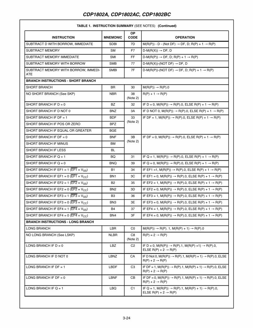
TABLE 1. INSTRUCTION SUMMARY (SEE NOTES)
INSTRUCTION MNEMONICOP
CODE OPERATION
MEMORY REFERENCE
LOAD VIA N LDN 0N M(R(N)) → D; FOR N not 0
LOAD ADVANCE LDA 4N M(R(N)) → D; R(N) + 1 → R(N)
LOAD VIA X LDX F0 M(R(X)) → D
LOAD VIA X AND ADVANCE LDXA 72 M(R(X)) → D; R(X) + 1 → R(X)
LOAD IMMEDIATE LDl F8 M(R(P)) → D; R(P) + 1 → R(P)
STORE VIA N STR 5N D → M(R(N))
STORE VIA X AND DECREMENT STXD 73 D → M(R(X)); R(X) - 1 → R(X)
REGISTER OPERATIONS
INCREMENT REG N INC 1N R(N) + 1 → R(N)
DECREMENT REG N DEC 2N R(N) - 1 → R(N)
INCREMENT REG X IRX 60 R(X) + 1 → R(X)
GET LOW REG N GLO 8N R(N).0 → D
PUT LOW REG N PLO AN D → R(N).0
GET HIGH REG N GHl 9N R(N).1 → D
PUT HIGH REG N PHI BN D → R(N).1
LOGIC OPERATIONS (Note 1)
OR OR F1 M(R(X)) OR D → D
OR IMMEDIATE ORl F9 M(R(P)) OR D → D; R(P) + 1 → R(P)
EXCLUSIVE OR XOR F3 M(R(X)) XOR D → D
EXCLUSIVE OR IMMEDIATE XRI FB M(R(P)) XOR D → D; R(P) + 1 → R(P)
AND AND F2 M(R(X)) AND D → D
AND IMMEDIATE ANl FA M(R(P)) AND D → D; R(P) + 1 → R(P)
SHIFT RIGHT SHR F6 SHIFT D RIGHT, LSB(D) → DF, 0 → MSB(D)
SHIFT RIGHT WITH CARRY SHRC 76(Note 2)
SHIFT D RIGHT, LSB(D) → DF, DF → MSB(D)
RING SHIFT RIGHT RSHR 76(Note 2)
SHIFT D RIGHT, LSB(D) → DF, DF → MSB(D)
SHIFT LEFT SHL FE SHIFT D LEFT, MSB(D) → DF, 0 → LSB(D)
SHIFT LEFT WITH CARRY SHLC 7E(Note 2)
SHIFT D LEFT, MSB(D) → DF, DF → LSB(D)
RING SHIFT LEFT RSHL 7E(Note 2)
SHIFT D LEFT, MSB(D) → DF, DF → LSB(D)
ARITHMETIC OPERATIONS (Note 1)
ADD ADD F4 M(R(X)) + D → DF, D
ADD IMMEDIATE ADl FC M(R(P)) + D → DF, D; R(P) + 1 → R(P)
ADD WITH CARRY ADC 74 M(R(X)) + D + DF → DF, D
ADD WITH CARRY, IMMEDIATE ADCl 7C M(R(P)) + D + DF → DF, D; R(P) + 1 → R(P)
SUBTRACT D SD F5 M(R(X)) - D → DF, D
SUBTRACT D IMMEDIATE SDl FD M(R(P)) - D → DF, D; R(P) + 1 → R(P)
SUBTRACT D WITH BORROW SDB 75 M(R(X)) - D - (NOT DF) → DF, D
CDP1802A, CDP1802AC, CDP1802BC
3-24
SUBTRACT D WITH BORROW, IMMEDIATE SDBl 7D M(R(P)) - D - (Not DF) → DF, D; R(P) + 1 → R(P)
SUBTRACT MEMORY SM F7 D-M(R(X)) → DF, D
SUBTRACT MEMORY IMMEDIATE SMl FF D-M(R(P)) → DF, D; R(P) + 1 → R(P)
SUBTRACT MEMORY WITH BORROW SMB 77 D-M(R(X))-(NOT DF) → DF, D
SUBTRACT MEMORY WITH BORROW, IMMEDI-ATE
SMBl 7F D-M(R(P))-(NOT DF) → DF, D; R(P) + 1 → R(P)
BRANCH INSTRUCTIONS - SHORT BRANCH
SHORT BRANCH BR 30 M(R(P)) → R(P).0
NO SHORT BRANCH (See SKP) NBR 38(Note 2)
R(P) + 1 → R(P)
SHORT BRANCH IF D = 0 BZ 32 IF D = 0, M(R(P)) → R(P).0, ELSE R(P) + 1 → R(P)
SHORT BRANCH IF D NOT 0 BNZ 3A IF D NOT 0, M(R(P)) → R(P).0, ELSE R(P) + 1 → R(P)
SHORT BRANCH IF DF = 1 BDF 33(Note 2)
IF DF = 1, M(R(P)) → R(P).0, ELSE R(P) + 1 → R(P)
SHORT BRANCH IF POS OR ZERO BPZ
SHORT BRANCH IF EQUAL OR GREATER BGE
SHORT BRANCH IF DF = 0 BNF 3B(Note 2)
IF DF = 0, M(R(P)) → R(P).0, ELSE R(P) + 1 → R(P)
SHORT BRANCH IF MINUS BM
SHORT BRANCH IF LESS BL
SHORT BRANCH IF Q = 1 BQ 31 IF Q = 1, M(R(P)) → R(P).0, ELSE R(P) + 1 → R(P)
SHORT BRANCH IF Q = 0 BNQ 39 IF Q = 0, M(R(P)) → R(P).0, ELSE R(P) + 1 → R(P)
SHORT BRANCH IF EF1 = 1 (EF1 = VSS) B1 34 IF EF1 =1, M(R(P)) → R(P).0, ELSE R(P) + 1 → R(P)
SHORT BRANCH IF EF1 = 0 (EF1 = VCC) BN1 3C IF EF1 = 0, M(R(P)) → R(P).0, ELSE R(P) + 1 → R(P)
SHORT BRANCH IF EF2 = 1 (EF2 = VSS) B2 35 IF EF2 = 1, M(R(P)) → R(P).0, ELSE R(P) + 1 → R(P)
SHORT BRANCH IF EF2 = 0 (EF2 = VCC) BN2 3D IF EF2 = 0, M(R(P)) → R(P).0, ELSE R(P) + 1 → R(P)
SHORT BRANCH IF EF3 = 1 (EF3 = VSS) B3 36 IF EF3 = 1, M(R(P)) → R(P).0, ELSE R(P) + 1 → R(P)
SHORT BRANCH IF EF3 = 0 (EF3 = VCC) BN3 3E IF EF3 = 0, M(R(P)) → R(P).0, ELSE R(P) + 1 → R(P)
SHORT BRANCH IF EF4 = 1 (EF4 = VSS) B4 37 IF EF4 = 1, M(R(P)) → R(P).0, ELSE R(P) + 1 → R(P)
SHORT BRANCH IF EF4 = 0 (EF4 = VCC) BN4 3F IF EF4 = 0, M(R(P)) → R(P).0, ELSE R(P) + 1 → R(P)
BRANCH INSTRUCTIONS - LONG BRANCH
LONG BRANCH LBR C0 M(R(P)) → R(P). 1, M(R(P) + 1) → R(P).0
NO LONG BRANCH (See LSKP) NLBR C8(Note 2)
R(P) = 2 → R(P)
LONG BRANCH IF D = 0 LBZ C2 lF D = 0, M(R(P)) → R(P).1, M(R(P) +1) → R(P).0,ELSE R(P) + 2 → R(P)
LONG BRANCH IF D NOT 0 LBNZ CA IF D Not 0, M(R(P))→ R(P).1, M(R(P) + 1)→ R(P).0, ELSER(P) + 2 → R(P)
LONG BRANCH IF DF = 1 LBDF C3 lF DF = 1, M(R(P))→ R(P).1, M(R(P) + 1)→ R(P).0, ELSER(P) + 2 → R(P)
LONG BRANCH IF DF = 0 LBNF CB IF DF = 0, M(R(P))→ R(P).1, M(R(P) + 1)→ R(P).0, ELSER(P) + 2 → R(P)
LONG BRANCH IF Q = 1 LBQ C1 IF Q = 1, M(R(P)) → R(P).1, M(R(P) + 1) → R(P).0,ELSE R(P) + 2 → R(P)
TABLE 1. INSTRUCTION SUMMARY (SEE NOTES) (Continued)
INSTRUCTION MNEMONICOP
CODE OPERATION
CDP1802A, CDP1802AC, CDP1802BC

3-25
LONG BRANCH lF Q = 0 LBNQ C9 lF Q = 0, M(R(P)) → R(P).1, M(R(P) + 1) → R(P).0EISE R(P) + 2 → R(P)
SKIP INSTRUCTIONS
SHORT SKIP (See NBR) SKP 38(Note 2)
R(P) + 1 → R(P)
LONG SKIP (See NLBR) LSKP C8(Note 2)
R(P) + 2 → R(P)
LONG SKIP IF D = 0 LSZ CE IF D = 0, R(P) + 2 → R(P), ELSE CONTINUE
LONG SKIP IF D NOT 0 LSNZ C6 IF D Not 0, R(P) + 2 → R(P), ELSE CONTINUE
LONG SKIP IF DF = 1 LSDF CF IF DF = 1, R(P) + 2 → R(P), ELSE CONTINUE
LONG SKIP IF DF = 0 LSNF C7 IF DF = 0, R(P) + 2 → R(P), ELSE CONTINUE
LONG SKIP lF Q = 1 LSQ CD IF Q = 1, R(P) + 2 → R(P), ELSE CONTINUE
LONG SKIP IF Q = 0 LSNQ C5 IF Q = 0, R(P) + 2 → R(P), ELSE CONTINUE
LONG SKIP IF lE = 1 LSlE CC IF IE = 1, R(P) + 2 → R(P), ELSE CONTINUE
CONTROL INSTRUCTIONS
IDLE lDL 00(Note 3)
WAIT FOR DMA OR INTERRUPT; M(R(0)) → BUS
NO OPERATION NOP C4 CONTINUE
SET P SEP DN N → P
SET X SEX EN N → X
SET Q SEQ 7B 1 → Q
RESET Q REQ 7A 0 → Q
SAVE SAV 78 T → M(R(X))
PUSH X, P TO STACK MARK 79 (X, P) → T; (X, P) → M(R(2)), THEN P → X; R(2) - 1 → R(2)
RETURN RET 70 M(R(X)) → (X, P); R(X) + 1 → R(X), 1 → lE
DISABLE DlS 71 M(R(X)) → (X, P); R(X) + 1 → R(X), 0 → lE
INPUT - OUTPUT BYTE TRANSFER
OUTPUT 1 OUT 1 61 M(R(X)) → BUS; R(X) + 1 → R(X); N LINES = 1
OUTPUT 2 OUT 2 62 M(R(X)) → BUS; R(X) + 1 → R(X); N LINES = 2
OUTPUT 3 OUT 3 63 M(R(X)) → BUS; R(X) + 1 → R(X); N LINES = 3
OUTPUT 4 OUT 4 64 M(R(X)) → BUS; R(X) + 1 → R(X); N LINES = 4
OUTPUT 5 OUT 5 65 M(R(X)) → BUS; R(X) + 1 → R(X); N LINES = 5
OUTPUT 6 OUT 6 66 M(R(X)) → BUS; R(X) + 1 → R(X); N LINES = 6
OUTPUT 7 OUT 7 67 M(R(X)) → BUS; R(X) + 1 → R(X); N LINES = 7
INPUT 1 INP 1 69 BUS → M(R(X)); BUS → D; N LINES = 1
INPUT 2 INP 2 6A BUS → M(R(X)); BUS → D; N LINES = 2
INPUT 3 INP 3 6B BUS → M(R(X)); BUS → D; N LINES = 3
INPUT 4 INP 4 6C BUS → M(R(X)); BUS → D; N LINES = 4
INPUT 5 INP 5 6D BUS → M(R(X)); BUS → D; N LINES = 5
INPUT 6 INP 6 6E BUS → M(R(X)); BUS → D; N LINES = 6
INPUT 7 INP 7 6F BUS → M(R(X)); BUS → D; N LINES = 7
TABLE 1. INSTRUCTION SUMMARY (SEE NOTES) (Continued)
INSTRUCTION MNEMONICOP
CODE OPERATION
CDP1802A, CDP1802AC, CDP1802BC
Dave Ruske

3-26
NOTES: (For Table 1)1. The arithmetic operations and the shift instructions are the only instructions that can alter the DF.
After an add instruction:DF = 1 denotes a carry has occurredDF = 0 Denotes a carry has not occurredAfter a subtract instruction:DF = 1 denotes no borrow. D is a true positive numberDF = 0 denotes a borrow. D is two’s complementThe syntax “-(not DF)” denotes the subtraction of the borrow.
2. This instruction is associated with more than one mnemonic. Each mnemonic is individually listed.3. An idle instruction initiates a repeating S1 cycle. The processor will continue to idle until an I/O request (INTERRUPT, DMA-lN, or DMA- OUT) is
activated. When the request is acknowledged, the idle cycle is terminated and the I/O request is serviced, and then normal operation is resumed.4. Long-Branch, Long-Skip and No Op instructions require three cycles to complete (1 fetch + 2 execute).
Long-Branch instructions are three bytes long. The first byte specifies the condition to be tested; and the second and third byte, thebranching address.The long-branch instructions can:a. Branch unconditionallyb. Test for D = 0 or D ≠ 0c. Test for DF = 0 or DF = 1d. Test for Q = 0 or Q = 1e. Effect an unconditional no branchIf the tested condition is met, then branching takes place; the branching address bytes are loaded in the high-and-low order bytes of thecurrent program counter, respectively. This operation effects a branch to any memory location.If the tested condition is not met, the branching address bytes are skipped over, and the next instruction in sequence is fetched and exe-cuted. This operation is taken for the case of unconditional no branch (NLBR).
5. The short-branch instructions are two bytes long. The first byte specifies the condition to be tested, and the second specifies the branching address.The short branch instruction can:a. Branch unconditionallyb. Test for D = 0 or D ≠ 0c. Test for DF = 0 or DF = 1d. Test for Q = 0 or Q = 1e. Test the status (1 or 0) of the four EF flagsf. Effect an unconditional no branchIf the tested condition is met, then branching takes place; the branching address byte is loaded into the low-order byte position of thecurrent program counter. This effects a branch within the current 256-byte page of the memory, i.e., the page which holds the branchingaddress. If the tested condition is not met, the branching address byte is skipped over, and the next instruction in sequence is fetchedand executed. This same action is taken in the case of unconditional no branch (NBR).
6. The skip instructions are one byte long. There is one Unconditional Short-Skip (SKP) and eight Long-Skip instructions.
The Unconditional Short-Skip instruction takes 2 cycles to complete (1 fetch + 1 execute). Its action is to skip over the byte following it.Then the next instruction in sequence is fetched and executed. This SKP instruction is identical to the unconditional no-branch instruc-tion (NBR) except that the skipped-over byte is not considered part of the program.The Long-Skip instructions take three cycles to complete (1 fetch + 2 execute).
They can:a. Skip unconditionallyb. Test for D = 0 or D ≠ 0c. Test for DF = 0 or DF = 1d. Test for Q = 0 or Q = 1e. Test for IE = 1
If the tested condition is met, then Long Skip takes place; the current program counter is incremented twice. Thus two bytes are skippedover, and the next instruction in sequence is fetched and executed. If the tested condition is not met, then no action is taken. Executionis continued by fetching the next instruction in sequence.
TABLE 1. INSTRUCTION SUMMARY (SEE NOTES) (Continued)
INSTRUCTION MNEMONICOP
CODE OPERATION
CDP1802A, CDP1802AC, CDP1802BC

3-27
TABLE 2. CONDITIONS ON DATA BUS AND MEMORY ADDRESS LINES DURING ALL MACHINE STATES
STATE I N SYMBOL OPERATIONDATABUS
MEMORYADDRESS MRD MWR
NLINES NOTES
S1 RESET 0 → I, N, Q, X, P; 1 → lE 00 XXXX 1 1 0 1
Initialize, Not ProgrammerAccessible
0000 → R 00 XXXX 1 1 0 2
S0 FETCH MRP → l, N; RP + 1 → RP MRP RP 0 1 0 3
S1 0 0 lDL IDLE MR0 RO 0 1 0 4, Fig. 8
0 1 - F LDN MRN → D MRN RN 0 1 0 Fig. 8
1 0 - F INC RN + 1 → RN Float RN 1 1 0 Fig. 6
2 0 - F DEC RN - 1 → RN Float RN 1 1 0 Fig. 6
3 0 - F Short Branch Taken: MRP → RP.0Not Taken; RP + 1 → RP
MRP RP 0 1 0 Fig. 8
4 0 - F LDA MRN → D; RN + 1 → RN MRN RN 0 1 0 Fig. 8
5 0 - F STR D → MRN D RN 1 0 0 Fig. 7
6 0 IRX RX + 1 → RX MRX RX 0 1 0 Fig. 7
6 1 OUT 1 MRX → BUS; RX + 1 → RX MRX RX 0 1 1 Fig. 11
2 OUT 2 2 Fig. 11
3 OUT 3 3 Fig. 11
4 OUT 4 4 Fig. 11
5 OUT 5 5 Fig. 11
6 OUT 6 6 Fig. 11
7 OUT 7 7 Fig. 11
9 INP 1 BUS → MRX, D Data fromI/O Device
RX 1 0 1 Fig. 10
A INP 2 2 Fig. 10
B INP 3 3 Fig. 10
C INP 4 4 Fig. 10
D INP5 5 Fig. 10
E INP6 6 Fig. 10
F INP7 7 Fig. 10
7 0 RET MRX → (X, P); RX + 1 → RX;1 → lE
MRX RX 0 1 0 Fig. 8
1 DlS MRX → (X, P); RX + 1 → RX;0 → lE
MRX RX 0 1 0 Fig. 8
2 LDXA MRX → D; RX + 1 → RX MRX RX 0 1 0 Fig. 8
3 STXD D → MRX; RX - 1 → RX D RX 1 0 0 Fig. 7
4 ADC MRX + D + DF → DF, D MRX RX 0 1 0 Fig. 8
5 SDB MRX - D - DFN → DF, D MRX RX 0 1 0 Fig. 8
6 SHRC LSB(D) → DF; DF → MSB(D) Float RX 1 1 0 Fig. 6
7 SMB D - MRX - DFN → DF, D MRX RX 0 1 0 Fig. 8
8 SAV T → MRX T RX 1 0 0 Fig. 7
CDP1802A, CDP1802AC, CDP1802BC

3-28
S1 7 9 MARK (X, P) → T, MR2; P → X;R2 - 1 → R2
T R2 1 0 0 Fig. 7
A REQ 0 → Q Float RP 1 1 0 Fig. 6
B SEQ 1 → Q Float RP 1 1 0 Fig. 6
C ADCl MRP + D + DF → DF, D;RP + 1
MRP RP 0 1 0 Fig. 8
D SDBl MRP - D - DFN → DF, D;RP + 1
MRP RP 0 1 0 Fig. 8
E SHLC MSB(D) → DF; DF → LSB(D) Float RP 1 1 0 Fig. 6
F SMBl D - MRP - DFN → DF, D;RP + 1
MRP RP 0 1 0 Fig. 8
8 0 - F GLO RN.0 → D RN.0 RN 1 1 0 Fig. 6
9 0 - F GHl RN.1 → D RN.1 RN 1 1 0 Fig. 6
A 0 - F PLO D → RN.0 D RN 1 1 0 Fig. 6
B 0 - F PHI D → RN.1 D RN 1 1 0 Fig. 6
S1#1 C 0 - 3,8 - B
Long Branch Taken: MRP → B; RP + 1 →RP
MRP RP 0 1 0 Fig. 9
#2 Taken: B → RP.1;MRP → RP.0
M(RP + 1) RP + 1 0 1 0 Fig. 9
S1#1 Not Taken: RP + 1 → RP MRP RP 0 1 0 Fig. 9
#2 Not Taken: RP + 1 → RP M(RP + 1) RP + 1 0 1 0 Fig. 9
S1#1 567CDEF
Long Skip Taken: RP + 1 → RP MRP RP 0 1 0 Fig. 9
#2 Taken: RP + 1 → RP M(RP + 1) RP + 1 0 1 0 Fig. 9
S1#1 Not Taken: No Operation MRP RP 0 1 0 Fig. 9
#2 Not Taken: No Operation MRP RP 0 1 0 Fig. 9
S1#1 4 NOP No Operation MRP RP 0 1 0 Fig. 9
#2 No Operation MRP RP 0 1 0 Fig. 9
S1 D 0 - F SEP N → P NN RN 1 1 0 Fig. 6
E 0 - F SEX N → X NN RN 1 1 0 Fig. 6
S1 F 0 LDX MRX → D MRX RX 0 1 0 Fig. 8
123457
ORANDXORADDSDSM
MRX OR D → DMRX AND D → DMRX XOR D → DMRX + D → DF, DMRX - D → DF, DD - MRX → DF, D
MRX RX 0 1 0 Fig. 8
6 SHR LSB(D) → DF; 0 → MSB(D) Float RX 1 1 0 Fig. 6
TABLE 2. CONDITIONS ON DATA BUS AND MEMORY ADDRESS LINES DURING ALL MACHINE STATES (Continued)
STATE I N SYMBOL OPERATIONDATABUS
MEMORYADDRESS MRD MWR
NLINES NOTES
CDP1802A, CDP1802AC, CDP1802BC

3-29
All Intersil semiconductor products are manufactured, assembled and tested under ISO9000 quality systems certification.Intersil products are sold by description only. Intersil Corporation reserves the right to make changes in circuit design and/or specifications at any time withoutnotice. Accordingly, the reader is cautioned to verify that data sheets are current before placing orders. Information furnished by Intersil is believed to be accurateand reliable. However, no responsibility is assumed by Intersil or its subsidiaries for its use; nor for any infringements of patents or other rights of third parties whichmay result from its use. No license is granted by implication or otherwise under any patent or patent rights of Intersil or its subsidiaries.
For information regarding Intersil Corporation and its products, see web site http://www.intersil.com
Operating and Handling ConsiderationsHandling
All inputs and outputs of Intersil CMOS devices have a net-work for electrostatic protection during handling.
Operating
Operating Voltage - During operation near the maximumsupply voltage limit care should be taken to avoid or suppresspower supply turn-on and turn-off transients, power supply rip-ple, or ground noise; any of these conditions must not causeVDD - VSS to exceed the absolute maximum rating.
Input Signals - To prevent damage to the input protectioncircuit, input signals should never be greater than VDD norless than VSS. Input currents must not exceed 10mA evenwhen the power supply is off.
Unused Inputs - A connection must be provided at everyinput terminal. All unused input terminals must be connectedto either VDD or VSS, whichever is appropriate.
Output Short Circuits - Shorting of outputs to VDD or VSSmay damage CMOS devices by exceeding the maximumdevice dissipation.
S1 F 8 LDl MRP → D; RP + 1 → RP MRP RP 0 1 0 Fig. 8
9 ORl MRP OR D→ D; RP + 1→ RP
A ANl MRP AND D→ D; RP + 1→ RP
B XRl MRP XOR D→ D; RP + 1→RP
C ADl MRP + D→ DF, D; RP + 1→RP
D SDl MRP - D → DF, D; RP + 1 →RP
F SMl D - MRP → DF, D; RP +1 →RP
E SHL MSB(D) → DF; 0 → LSB(D) Float RP 1 1 0 Fig. 6
S2 DMA IN BUS → MR0; R0 + 1 → R0 Data fromI/O Device
R0 1 0 0 6, Fig. 12
DMAOUT MR0 → BUS; R0 + 1 → R0 MR0 R0 0 1 0 6, Fig. 13
S3 INTERRUPT X, P → T; 0 → lE, 1 → P;2 → X
Float RN 1 1 0 Fig. 14
S1 LOAD IDLE (CLEAR, WAlT = 0) M(R0 - 1) R0 - 1 0 1 0 5, Fig. 8
NOTES:1. lE = 1, TPA, TPB suppressed, state = S1.2. BUS = 0 for entire cycle.3. Next state always S1.4. Wait for DMA or INTERRUPT.5. Suppress TPA, wait for DMA.6. IN REQUEST has priority over OUT REQUEST.7. See Timing Waveforms, Figure 5 through Figure 14 for machine cycles.
TABLE 2. CONDITIONS ON DATA BUS AND MEMORY ADDRESS LINES DURING ALL MACHINE STATES (Continued)
STATE I N SYMBOL OPERATIONDATABUS
MEMORYADDRESS MRD MWR
NLINES NOTES
CDP1802A, CDP1802AC, CDP1802BC