CCDFundamentals RefDoc PS-0046 r1.0
22
CCD FUNDAMENTALS AUGUST 3, 2012 REFERENCE DOCUMENT REVISION 1.0 PS-0046
-
Upload
rocketzhen -
Category
Documents
-
view
233 -
download
1
Transcript of CCDFundamentals RefDoc PS-0046 r1.0

CCD FUNDAMENTALS
AUGUST 3, 2012
REFERENCE DOCUMENT
REVISION 1.0 PS-0046

CCD Fundamentals
www.truesenseimaging.com Revision 1.0 PS-0046 Pg 2
TABLE OF CONTENTS
Introduction ............................................................................................................................................................................................................... 4 CCD Formats .............................................................................................................................................................................................................. 4
Point Scanning .............................................................................................................................................................................................. 4
Line Scanning ................................................................................................................................................................................................ 5 Area Scanning ............................................................................................................................................................................................... 6
CCD Architectures .................................................................................................................................................................................................. 6 Full-Frame (FF) ............................................................................................................................................................................................. 6 Frame-Transfer (FT) .................................................................................................................................................................................... 7 Interline (IL) ................................................................................................................................................................................................... 8
CCD Basics .................................................................................................................................................................................................................. 9 Converting Light (Photons) to Electronic Charge ............................................................................................................................... 9 Potential Wells and Barriers .................................................................................................................................................................. 10 Charge Transfer Techniques .................................................................................................................................................................. 10 Four-Phase (4φ) CCD ............................................................................................................................................................................... 10 Three-Phase (3φ) CCD ............................................................................................................................................................................. 12 Pseudo Two-Phase (P2φ) CCD .............................................................................................................................................................. 13 True Two-Phase (T2φ) CCD .................................................................................................................................................................... 14 Virtual Phase (Vφ) CCD ........................................................................................................................................................................... 15
Readout Techniques ................................................................................................................................................................................ 16 Related CCD Enhancing Technologies ......................................................................................................................................................... 17
Color CCD Imaging ................................................................................................................................................................................... 17
Color Sequential ....................................................................................................................................................................................... 17 Three-Chip Color ....................................................................................................................................................................................... 17 Integral Color Filter Arrays (CFA) ......................................................................................................................................................... 18 Anti-blooming ............................................................................................................................................................................................ 18 Vertical Overflow Drain (VOD) .............................................................................................................................................................. 19 Lateral Overflow Drain (LOD) ................................................................................................................................................................ 19 Silicon Thinning ......................................................................................................................................................................................... 20 UV Enhancement Coatings ..................................................................................................................................................................... 20 Microlenticular Arrays ............................................................................................................................................................................. 21
High Speed CCDs ...................................................................................................................................................................................... 21 Revision Changes................................................................................................................................................................................................... 22
MTD/PS-0218 ............................................................................................................................................................................................. 22 PS-0046 ....................................................................................................................................................................................................... 22
CCD Fundamentals
www.truesenseimaging.com Revision 1.0 PS-0046 Pg 3
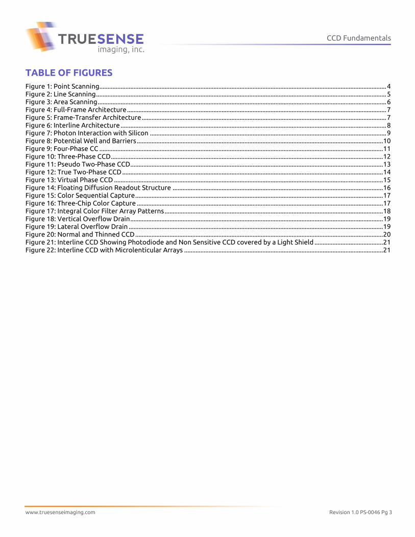
TABLE OF FIGURES
Figure 1: Point Scanning ................................................................................................................................................................................ 4 Figure 2: Line Scanning .................................................................................................................................................................................. 5 Figure 3: Area Scanning ................................................................................................................................................................................. 6 Figure 4: Full-Frame Architecture ............................................................................................................................................................... 7 Figure 5: Frame-Transfer Architecture ...................................................................................................................................................... 7 Figure 6: Interline Architecture ................................................................................................................................................................... 8 Figure 7: Photon Interaction with Silicon ................................................................................................................................................. 9 Figure 8: Potential Well and Barriers ....................................................................................................................................................... 10 Figure 9: Four-Phase CC .............................................................................................................................................................................. 11 Figure 10: Three-Phase CCD ....................................................................................................................................................................... 12 Figure 11: Pseudo Two-Phase CCD ........................................................................................................................................................... 13 Figure 12: True Two-Phase CCD ................................................................................................................................................................ 14 Figure 13: Virtual Phase CCD ..................................................................................................................................................................... 15 Figure 14: Floating Diffusion Readout Structure ................................................................................................................................. 16 Figure 15: Color Sequential Capture ........................................................................................................................................................ 17 Figure 16: Three-Chip Color Capture ....................................................................................................................................................... 17 Figure 17: Integral Color Filter Array Patterns ...................................................................................................................................... 18 Figure 18: Vertical Overflow Drain ........................................................................................................................................................... 19 Figure 19: Lateral Overflow Drain ............................................................................................................................................................ 19 Figure 20: Normal and Thinned CCD ........................................................................................................................................................ 20 Figure 21: Interline CCD Showing Photodiode and Non Sensitive CCD covered by a Light Shield .......................................... 21 Figure 22: Interline CCD with Microlenticular Arrays .......................................................................................................................... 21

CCD Fundamentals
www.truesenseimaging.com Revision 1.0 PS-0046 Pg 4
Introduction This primer is intended for those involved with CCD image sensing applications wishing to obtain additional insight into
the mechanisms of CCD sensor principles and operations. It is not intended to provide an exhaustive study into the
detailed theory behind the subject and it is assumed that a silicon based CCD is used unless otherwise stated. It is also
assumed that a conventional front illuminated detector system is employed. Some references are listed at the
conclusion.
Like many technologies, the Charge-Coupled Device (CCD) started out as one kind of creature and wound up as
something completely different. Invented in the late 1960's by researchers at Bell Labs, it was initially conceived as a
new type of computer memory circuit, and it was demonstrated in 1970 for that facility. It soon became apparent that
the CCD had many other potential applications, including signal processing and imaging, the latter because of silicon's
light sensitivity that responds to wavelengths less than 1.1 µm (the visible spectrum falls between 0.4 µm and 0.7 µm).
The CCD's early promise as a memory element has since disappeared, but its superb ability to detect light has turned
the CCD into the premier image sensor technology.
Similarly to integrated circuits (IC), CCDs begin on thin silicon wafers that are processed with a series of elaborate
steps, which define the various functions within the circuit. Each wafer contains several identical devices (“chips”), each
capable of yielding a functional device. Selected chips, based on a variety of preliminary screening tests, are then cut
from the wafer and packaged into a carrier for use in a system.
The scope of this primer is to introduce the reader to the basics of CCD imaging. The qualitative discussions described
herein reflect silicon based imaging applications in the visible spectrum.
CCD Formats Image sensing can be performed using three basic techniques: point scanning, line scanning and area scanning. CCDs,
by their definition, can take the form of line and area scanning formats.
POINT SCANNING Using a single cell detector or pixel (picture element), an image can be scanned by sequentially detecting scene
information at discrete XY coordinates. Advantages to this approach are high resolution, uniformity of measurement
from one site to another, and the cost/simplicity of the detector. Disadvantages include registration errors from the
XY movement of scene or detector, frame-scanning rates because of the repeated number of exposures, and system
complexity due to the X-Y movement (see Figure 1).
Figure 1: Point Scanning
IMAGE SCENE
POINT SCANNER
CCD Fundamentals
www.truesenseimaging.com Revision 1.0 PS-0046 Pg 5
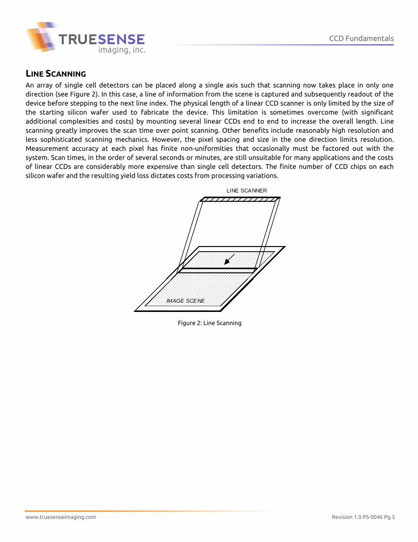
LINE SCANNING An array of single cell detectors can be placed along a single axis such that scanning now takes place in only one
direction (see Figure 2). In this case, a line of information from the scene is captured and subsequently readout of the
device before stepping to the next line index. The physical length of a linear CCD scanner is only limited by the size of
the starting silicon wafer used to fabricate the device. This limitation is sometimes overcome (with significant
additional complexities and costs) by mounting several linear CCDs end to end to increase the overall length. Line
scanning greatly improves the scan time over point scanning. Other benefits include reasonably high resolution and
less sophisticated scanning mechanics. However, the pixel spacing and size in the one direction limits resolution.
Measurement accuracy at each pixel has finite non-uniformities that occasionally must be factored out with the
system. Scan times, in the order of several seconds or minutes, are still unsuitable for many applications and the costs
of linear CCDs are considerably more expensive than single cell detectors. The finite number of CCD chips on each
silicon wafer and the resulting yield loss dictates costs from processing variations.
Figure 2: Line Scanning
IMAGE SCENE
LINE SCANNER

CCD Fundamentals
www.truesenseimaging.com Revision 1.0 PS-0046 Pg 6
AREA SCANNING A two dimensional array of detectors can be created such that the entire image can be captured with one exposure
eliminating the need for any movement by detector or scene (see Figure 3). Area scanners are capable of producing
the highest frame rates with the greatest amount of registration accuracy between pixels. System complexities are
also kept to a minimum. However, resolution is now limited in two directions. Other disadvantages include generally
lower signal-to-noise performance and cost because fewer devices can be placed on a wafer and yield is inherently
lower for a number of reasons.
Figure 3: Area Scanning
CCD Architectures CCDs can take on various architectures. The primary CCDs in use today are Full-Frame Transfer and Frame-Transfer
devices, which use MOS photocapacitors as detectors, and Interline Transfer devices which use photodiodes and
photocapacitors as the detector. Each is described below as applied to area CCD sensors but the concepts also apply to
linear CCDs. Other image sensing architectures, which will not be discussed here, include Frame-Interline Transfer,
Accordion, Charge Injection and MOS XY addressable among others.
FULL-FRAME (FF) Full-Frame CCDs have the simplest architecture and are the easiest to fabricate and operate. They consist of a parallel
CCD shift register, a serial CCD shift register and a signal sensing output amplifier (see Figure 4). Images are optically
projected onto the parallel array that acts as the image plane. The device takes the scene information and partitions
the image into discrete elements that are defined by the number of pixels thus "quantizing" the scene. The resulting
rows of scene information are then shifted in a parallel fashion to the serial register that subsequently shifts the row
of information to the output as a serial stream of data. The process repeats until all rows are transferred off chip. The
image is then reconstructed as dictated by the system. Since the parallel register is used for both scene detection and
readout, a mechanical shutter or synchronized strobe illumination must be used to preserve scene integrity. The
simplicity of the FF design yields CCD imagers with the highest resolution and highest density.
IMAGE SCENE
AREA SCANNER

CCD Fundamentals
www.truesenseimaging.com Revision 1.0 PS-0046 Pg 7
ONE
PIXEL
PARALLEL
CLOCKS
PARALLEL REGISTER
SERIAL REGISTERSERIAL
CLOCKS
OUTPUT
AMPLIFIER
DIRECTION
OF
PARALLEL
SHIFT
Figure 4: Full-Frame Architecture
FRAME-TRANSFER (FT) FT CCDs are very much like Full-Frame architectures (see Figure 5). The difference is that a separate and identical
parallel register, called a storage array, is added which is not light sensitive. The idea is to shift a captured scene from
the photosensitive, or image array, very quickly to the storage array. Readout off chip from the storage register is then
performed as previously described in the Full-Frame device while the storage array is integrating the next frame. The
advantage of this architecture is that a continuous or shutterless/strobeless operation is achieved resulting in faster
frame rates. The resulting performance is compromised, however, because integration is still occurring during the
image dump to the storage array resulting in image "smear". Since twice the silicon area is required to implement this
architecture, FT CCDs have lower resolutions and much higher costs than FF CCDs.
ONE
PIXELPIXEL
IMAGE ARRAY
PARALLEL
CLOCKS
DIRECTION
OF
PARALLEL
SHIFT
SERIAL REGISTERSERIAL
CLOCKS
OUTPUT
AMPLIFIER
STORAGE ARRAY
PARALLEL
CLOCKS
IMAGE ARRAY
STORAGE ARRAY
Figure 5: Frame-Transfer Architecture
CCD Fundamentals
www.truesenseimaging.com Revision 1.0 PS-0046 Pg 8
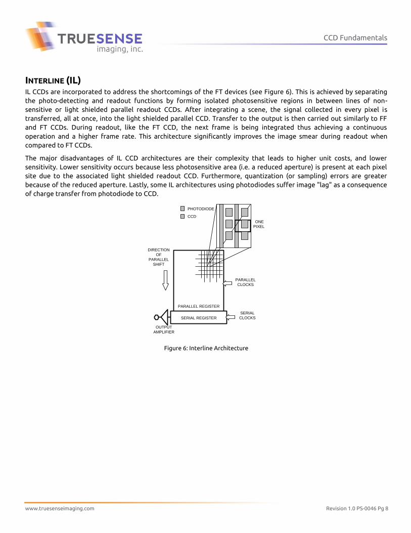
INTERLINE (IL) IL CCDs are incorporated to address the shortcomings of the FT devices (see Figure 6). This is achieved by separating
the photo-detecting and readout functions by forming isolated photosensitive regions in between lines of non-
sensitive or light shielded parallel readout CCDs. After integrating a scene, the signal collected in every pixel is
transferred, all at once, into the light shielded parallel CCD. Transfer to the output is then carried out similarly to FF
and FT CCDs. During readout, like the FT CCD, the next frame is being integrated thus achieving a continuous
operation and a higher frame rate. This architecture significantly improves the image smear during readout when
compared to FT CCDs.
The major disadvantages of IL CCD architectures are their complexity that leads to higher unit costs, and lower
sensitivity. Lower sensitivity occurs because less photosensitive area (i.e. a reduced aperture) is present at each pixel
site due to the associated light shielded readout CCD. Furthermore, quantization (or sampling) errors are greater
because of the reduced aperture. Lastly, some IL architectures using photodiodes suffer image "lag" as a consequence
of charge transfer from photodiode to CCD.
PARALLEL REGISTER
ONE
PIXEL
PARALLEL
CLOCKS
SERIAL REGISTER
SERIAL
CLOCKS
OUTPUT
AMPLIFIER
DIRECTION
OF
PARALLEL
SHIFT
PHOTODIODE
CCD
Figure 6: Interline Architecture
CCD Fundamentals
www.truesenseimaging.com Revision 1.0 PS-0046 Pg 9
CCD Basics CCD imaging is performed in a three step process:
(1) Exposure which converts light into an electronic charge at discrete sites called pixels;
(2) Charge transfer which moves the packets of charge within the silicon substrate; and,
(3) Charge to voltage conversion and output amplification.
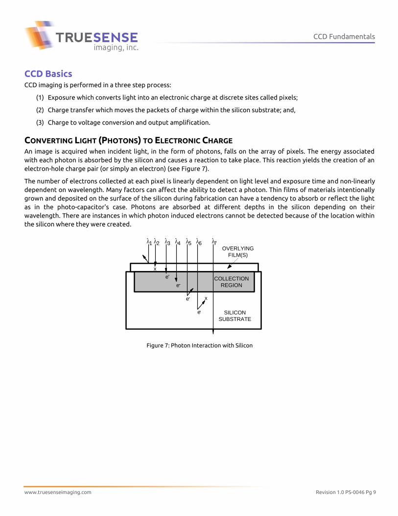
CONVERTING LIGHT (PHOTONS) TO ELECTRONIC CHARGE An image is acquired when incident light, in the form of photons, falls on the array of pixels. The energy associated
with each photon is absorbed by the silicon and causes a reaction to take place. This reaction yields the creation of an
electron-hole charge pair (or simply an electron) (see Figure 7).
The number of electrons collected at each pixel is linearly dependent on light level and exposure time and non-linearly
dependent on wavelength. Many factors can affect the ability to detect a photon. Thin films of materials intentionally
grown and deposited on the surface of the silicon during fabrication can have a tendency to absorb or reflect the light
as in the photo-capacitor's case. Photons are absorbed at different depths in the silicon depending on their
wavelength. There are instances in which photon induced electrons cannot be detected because of the location within
the silicon where they were created.
COLLECTION
REGION
e-
e-
e-
e-
x
x
OVERLYING
FILM(S)
SILICON
SUBSTRATE
l1 l2 l3 l4 l5 l6 l7
Figure 7: Photon Interaction with Silicon

CCD Fundamentals
www.truesenseimaging.com Revision 1.0 PS-0046 Pg 10
POTENTIAL WELLS AND BARRIERS CCDs follow the principles of basic Metal Oxide Semiconductor (MOS) device physics. A CCD MOS structure simply
consists of a vertically stacked conductive material (doped polysilicon) overlying a semiconductor (silicon) separated by
a highly insulating material (silicon dioxide). By applying a voltage potential to the polysilicon or "gate" electrode, the
electrostatic potentials within the silicon can be changed. With an appropriate voltage a potential "well" can be formed
which has the capability of collecting the localized electrons that were created by the incident light (see Figure 8). The
electrons can be confined under this gate by forming zones of higher potentials, called barriers, surrounding the well.
Depending on the voltage, each gate can be biased to form a potential well or a barrier to the integrated charge.
POTENTIAL
BARRIER
POTENTIAL
BARRIER
POTENTIAL
WELLPHOTOGENERATED
ELECTRONS
INCIDENT LIGHT
-V-V +V
POLYSILICONSILICON DIOXIDE
SILICON SUBSTRATE
Figure 8: Potential Well and Barriers
CHARGE TRANSFER TECHNIQUES Once charge has been integrated and held locally by the bounds of the pixel architecture, one must now have a means
of getting that charge to the sense amplifier which is physically separated from the pixels. The common methods used
today involve four differing charge transfer techniques that are described below. One thing to keep in mind as we walk
through these techniques is that as we move the charge associated with one pixel, we are at the same time moving all
the pixels associated with that row or column.
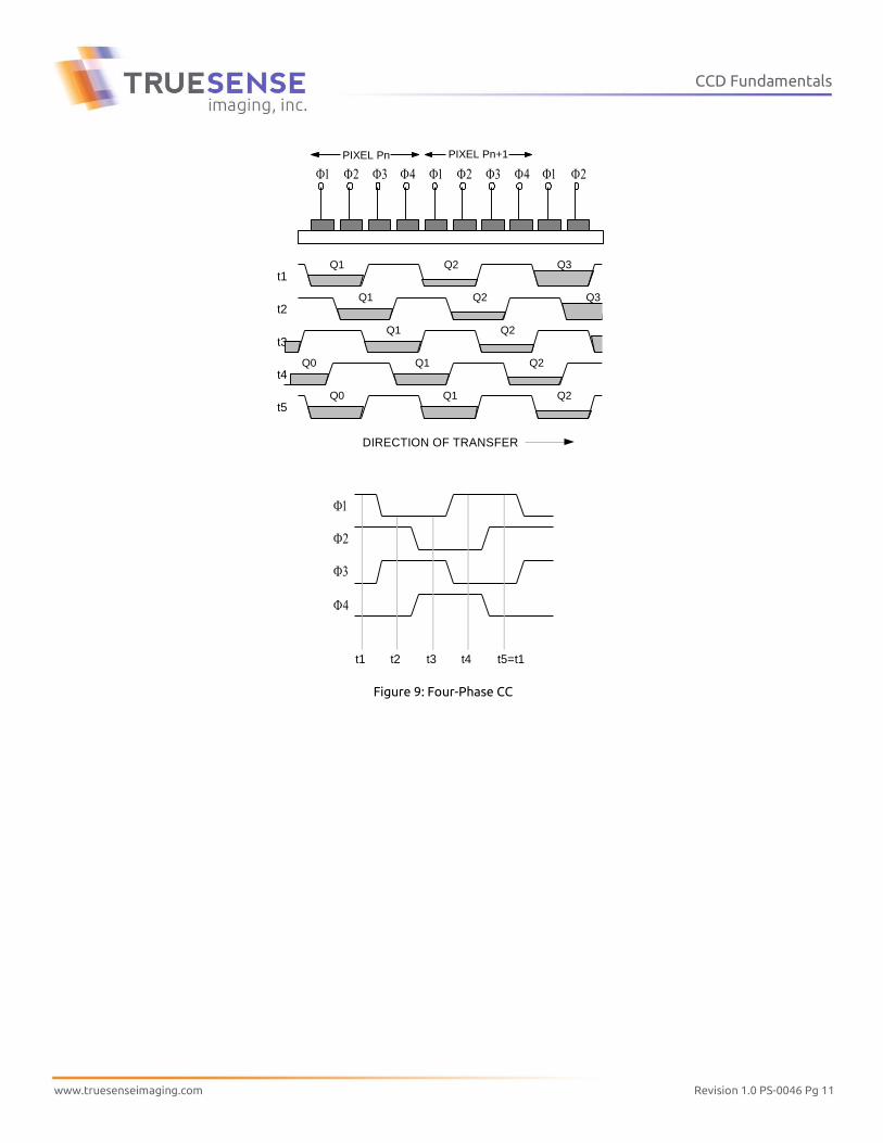
FOUR-PHASE (4Φ) CCD CCD shift registers are formed by defining polysilicon electrodes such that they form a long chain of gates along one
axis thereby forming a column. If a high level voltage is applied to one of these gates, a potential well is formed
beneath that gate while a low level voltage forms a potential barrier. Four gates are used to define a single pixel. As
the timing diagram (see Figure 9) shows during integration, if we hold the voltage on the φ1 and φ2 gates high while
keeping the voltage at the low level on the φ3 and φ4 gates, we can form a potential well which integrates and
collects photo-induced charge for pixel Pn. If φ1 and φ3 then change their polarity (i.e. φ1 goes from high to low and
φ2 goes from low to high) the charge packet is forced by electrostatics to move beneath φ2 and φ3. φ2 and φ4 now
reverse their polarity and the charge is moved further now occupying the well formed by the φ3 and φ4 electrode. This
process is carried out until the charge packet lies beneath the φ1 and φ2 gates of the next pixel, pn+1, thus completing
one transfer cycle. The cycle is repeated until all charge packets have reached the output. Thus 4 gates per pixel are
used.
CCD Fundamentals
www.truesenseimaging.com Revision 1.0 PS-0046 Pg 11
t1
t2
t3
t4
t5
F1 F2 F3 F4 F1 F2 F3 F4 F1 F2
Q1 Q2 Q3
Q2 Q3Q1
Q2Q1
Q2Q1
Q1 Q2Q0
Q0
PIXEL Pn PIXEL Pn+1
F1
F2
F3
F4
t1 t2 t3 t4 t5=t1
DIRECTION OF TRANSFER
Figure 9: Four-Phase CC
CCD Fundamentals
www.truesenseimaging.com Revision 1.0 PS-0046 Pg 12
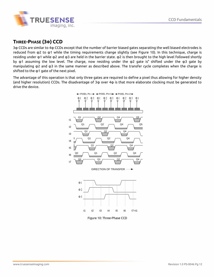
THREE-PHASE (3Φ) CCD 3φ CCDs are similar to 4φ CCDs except that the number of barrier biased gates separating the well biased electrodes is
reduced from φ2 to φ1 while the timing requirements change slightly (see Figure 10). In this technique, charge is
residing under φ1 while φ2 and φ3 are held in the barrier state. φ2 is then brought to the high level followed shortly
by φ1 assuming the low level. The charge, now residing under the φ2 gate is° shifted under the φ3 gate by
manipulating φ2 and φ3 in the same manner as described above. The transfer cycle completes when the charge is
shifted to the φ1 gate of the next pixel.
The advantage of this operation is that only three gates are required to define a pixel thus allowing for higher density
(and higher resolution) CCDs. The disadvantage of 3φ over 4φ is that more elaborate clocking must be generated to
drive the device.
F 1 F 2 F 3 F 1 F 2 F 3 F 1 F 2 F 3 F 1
Q1 Q2 Q4
PIXEL Pn PIXEL Pn+1 PIXEL Pn+2
Q5
Q1 Q2 Q4
Q1 Q2 Q4
Q1 Q2 Q4
Q1 Q2 Q4 Q5
Q1 Q2 Q4
Q1 Q2 Q4
Q0
Q0
Q0
Q0
t1
t2
t3
t4
t5
t6
t7
F 1
F 2
F 3
t1 t2 t3 t4 t5 t6 t7=t1
DIRECTION OF TRANSFER
Figure 10: Three-Phase CCD
CCD Fundamentals
www.truesenseimaging.com Revision 1.0 PS-0046 Pg 13
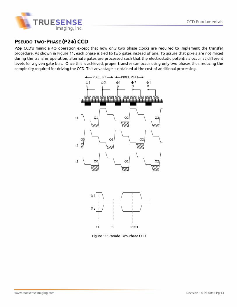
PSEUDO TWO-PHASE (P2Φ) CCD P2φ CCD's mimic a 4φ operation except that now only two phase clocks are required to implement the transfer
procedure. As shown in Figure 11, each phase is tied to two gates instead of one. To assure that pixels are not mixed
during the transfer operation, alternate gates are processed such that the electrostatic potentials occur at different
levels for a given gate bias. Once this is achieved, proper transfer can occur using only two phases thus reducing the
complexity required for driving the CCD. This advantage is obtained at the cost of additional processing.
F 1 F 2 F 1 F 2 F 1
Q1 Q2
PIXEL Pn PIXEL Pn+1
t1 Q3
Q1 Q2
Q0 Q1t3 Q2
t2
Q0
F 1
F 2
t1 t2 t3=t1
Figure 11: Pseudo Two-Phase CCD

CCD Fundamentals
www.truesenseimaging.com Revision 1.0 PS-0046 Pg 14
TRUE TWO-PHASE (T2Φ) CCD T2φ reduces the number of gates per pixel and the number of CCD drive phases to only two as shown in Figure 12. This
is achieved by creating the stepped potential beneath each gate as contrasted with the P2φ wherein two adjacent
gates are required to form the stepped potential.
T2φ is clocked just like P2φ shown earlier except that T2φ technologies have the capacity for very high densities and
very high resolutions. The disadvantage is that the processing becomes more extensive thus adding cost.
F 1 F 2 F 1 F 2 F 1 F 2 F 1 F 2 F 1 F 2
PIXEL
Pn
F 1
F 2
t1 t2 t3=t1
PIXEL
Pn+1
PIXEL
Pn+2
PIXEL
Pn+3
PIXEL
Pn+4
Q1
Q1
Q1
Q2
Q2
Q2
Q3
Q3
Q3
Q0
Q0
Q4
Q4
Q4
Q5
Q5
t1
t2
t3
Figure 12: True Two-Phase CCD

CCD Fundamentals
www.truesenseimaging.com Revision 1.0 PS-0046 Pg 15
VIRTUAL PHASE (VΦ) CCD Vφ CCDs reduce the number of gates per pixel and the number of CCD drive phases to only one as shown in Figure 13.
Characteristic to Vφ CCDs is the absence of any polysilicon electrodes between the φ1 gate. This makes the Vφ CCD
inherently more sensitive to light (especially in the blue) because of the reduced overlying topography which could
absorb or reflect the light.
Charge transfer efficiency is preserved by creating a stepped and "pinned" potential within the silicon. High pixel
densities are achievable with this architecture also. Some disadvantages are the high clock swings required by φ1 and
some yet unresolved performance degradations presumably due to the multiple implant complexities.
Q2Q1
t1
t2
t3
Q1 Q2 Q3 Q4 Q5
Q1 Q2 Q3 Q4Q0
Q1 Q2 Q3 Q4Q0
DIRECTION OF TRANSFER
F1
t1 t2 t3=t1
F1 F1 F1 F1 F1
PIXEL
Pn
PIXEL
Pn+1PIXEL
Pn+2
PIXEL
Pn+3
PIXEL
Pn+4
Figure 13: Virtual Phase CCD
CCD Fundamentals
www.truesenseimaging.com Revision 1.0 PS-0046 Pg 16
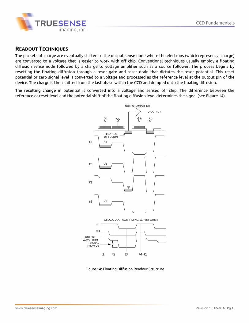
READOUT TECHNIQUES The packets of charge are eventually shifted to the output sense node where the electrons (which represent a charge)
are converted to a voltage that is easier to work with off chip. Conventional techniques usually employ a floating
diffusion sense node followed by a charge to voltage amplifier such as a source follower. The process begins by
resetting the floating diffusion through a reset gate and reset drain that dictates the reset potential. This reset
potential or zero signal level is converted to a voltage and processed as the reference level at the output pin of the
device. The charge is then shifted from the last phase within the CCD and dumped onto the floating diffusion.
The resulting change in potential is converted into a voltage and sensed off chip. The difference between the
reference or reset level and the potential shift of the floating diffusion level determines the signal (see Figure 14).
FLOATING
DIFFUSION
OUTPUT AMPLIFIER
OUTPUT
t1
t2
t3
Q1
Q1
Q1
t4 Q2
OUTPUT
WAVEFORM
CLOCK VOLTAGE TIMING WAVEFORMS
F1
FR
SIGNAL
FROM Q1
t4=t1t3t2t1
OGF1 FR RD
Figure 14: Floating Diffusion Readout Structure
CCD Fundamentals
www.truesenseimaging.com Revision 1.0 PS-0046 Pg 17
Related CCD Enhancing Technologies
COLOR CCD IMAGING Silicon based CCDs are monochrome in nature. That is they have no natural ability to determine the varying amounts of
red, green and blue (RGB) information presented to the pixels. One of three techniques may be used to extract color
information for a given scene. A common problem to any of the color imaging techniques described is that the amount
of information required triples.
COLOR SEQUENTIAL A color image can be created using a CCD by taking three successive exposures while switching in optical filters having
the desired RGB characteristics (see Figure 15). The resulting image is then reconstructed off chip. The advantage to
this technique is that resolution can remain that of the CCD itself. The disadvantage is that three exposures are
required reducing frame times by more than a factor of three. The filter switching assembly also adds to the
mechanical complexity of the system.
Figure 15: Color Sequential Capture
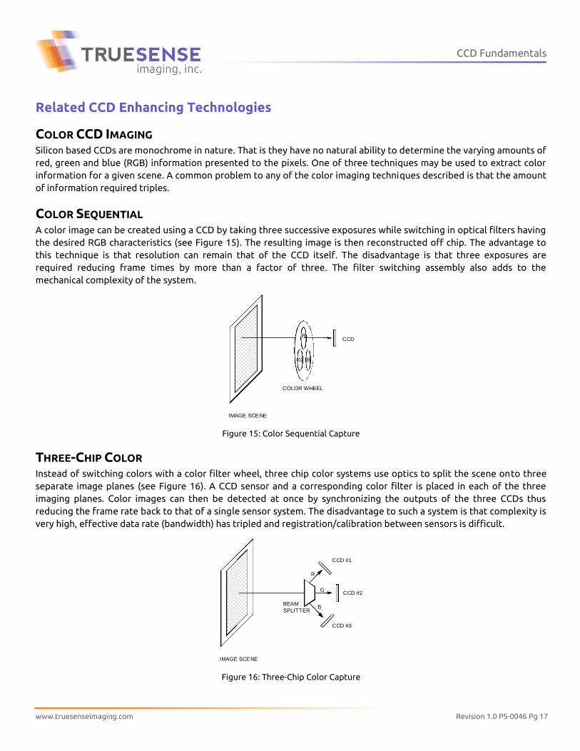
THREE-CHIP COLOR Instead of switching colors with a color filter wheel, three chip color systems use optics to split the scene onto three
separate image planes (see Figure 16). A CCD sensor and a corresponding color filter is placed in each of the three
imaging planes. Color images can then be detected at once by synchronizing the outputs of the three CCDs thus
reducing the frame rate back to that of a single sensor system. The disadvantage to such a system is that complexity is
very high, effective data rate (bandwidth) has tripled and registration/calibration between sensors is difficult.
Figure 16: Three-Chip Color Capture
R
G B
IMAGE SCENE
COLOR WHEEL
CCD
IMAGE SCENE
CCD #1
CCD #2
CCD #3
R
G
BBEAM
SPLITTER

CCD Fundamentals
www.truesenseimaging.com Revision 1.0 PS-0046 Pg 18
INTEGRAL COLOR FILTER ARRAYS (CFA) Instead of performing the color filtering off chip, filters of the appropriate characteristics can be placed on the chip
(see Figure 17). This approach can be performed during device fabrication using dyed (cyan, magenta, yellow)
photoresists in various patterns. The benefit of this approach is considerably reduced system complexity. The major
problem with this approach is that, unlike film, each pixel can only be patterned as one (primary color system RGB) or
two colors (secondary color systems CMY) or a combination. Any choice results in the loss of information leading to
reduced effective resolution and increased sampling (quantizing) artifacts. Another disadvantage is that off chip
processing is required to "fill in" the missing color information between pixels thus increasing system complexity.
IMAGE SCENE
CCD
G
G
G
G
G
G
G
G
R
R
R
R
B
B
B
BG
G
G
G
G
G
G
G
R
R
B
B
G
G
G
G
G
G
G
G
G
G
G
G
R
R
R
R
B
B
B
B
1 PIXEL
1 PIXEL
1 PIXEL
Figure 17: Integral Color Filter Array Patterns
ANTI-BLOOMING A problem with CCDs, unlike photographic film, is what happens when the device is over exposed. As mentioned
earlier, electrons are created at a linearly proportional rate of exposure. If the size of the potential wells created in the
CCD do not have the capacity to hold the integrated charge they will "bloom" or spill into adjacent pixels corrupting
scene information. This "blooming" can be alleviated by building "antiblooming" or overflow drain structures within
the device. Two common antiblooming structures are vertical overflow drains (VOD) and lateral overflow drains (LOD).
A side benefit of incorporating an overflow drain is the ability to use that feature to create a means of electronic
exposure or shutter control. Electronic exposure, which is much more accurate and reliable than mechanical shuttering,
allows very versatile operation for systems or cameras.

CCD Fundamentals
www.truesenseimaging.com Revision 1.0 PS-0046 Pg 19
VERTICAL OVERFLOW DRAIN (VOD) VOD devices have built-in electrostatic potential barriers to the biased substrate. The barrier is designed to a level that
is lower than the barriers between pixels. When collected charge exceeds this level it spills vertically through the
silicon and is swept away by the bias on the substrate (see Figure 18). Disadvantages of this structure are device
complexity, adding costs, and usually reduced well capacity leading to lower dynamic range.
Figure 18: Vertical Overflow Drain
LATERAL OVERFLOW DRAIN (LOD) One of the problems with VOD structures is that they have limited capacity in the amount of over exposure occurring.
For the most demanding situations, a LOD structure is used. LOD is implemented on the surface of the silicon where
the rest of the structures reside (see Figure 19).
In this case a barrier is created adjacent to the integrating pixels and charge spills into the drain laterally and swept off
chip. The disadvantage of such a structure is reduced fill factor or aperture leading to reduced photo-responsivity.
Figure 19: Lateral Overflow Drain
-- -- - -- - - -- - - - -- - -- - -- - - -- - - - - - -
-
-
DRAIN
- - - - - - - - - - - - - - - - - - - - - -- - - - - - - - - - - - - - - - - - - - - -- - - - - - - - - - - - - - - - - - - - - - -- - - - - - - - - - - - - - - - - - - - - - - - - - - - - - - - - - - - - - - - - - - - - - - - - - - - - - - --
-
-
DRAIN GATE F
CCD Fundamentals
www.truesenseimaging.com Revision 1.0 PS-0046 Pg 20
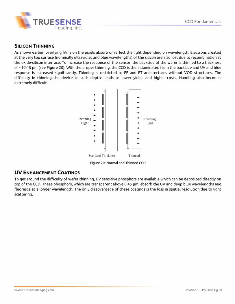
SILICON THINNING As shown earlier, overlying films on the pixels absorb or reflect the light depending on wavelength. Electrons created
at the very top surface (nominally ultraviolet and blue wavelengths) of the silicon are also lost due to recombination at
the oxide-silicon interface. To increase the response of the sensor, the backside of the wafer is thinned to a thickness
of ~10-15 µm (see Figure 20). With the proper thinning, the CCD is then illuminated from the backside and UV and blue
response is increased significantly. Thinning is restricted to FF and FT architectures without VOD structures. The
difficulty in thinning the device to such depths leads to lower yields and higher costs. Handling also becomes
extremely difficult.
Incoming
Light
Incoming
Light
Standard Thickness Thinned
Figure 20: Normal and Thinned CCD
UV ENHANCEMENT COATINGS To get around the difficulty of wafer thinning, UV sensitive phosphors are available which can be deposited directly on
top of the CCD. These phosphors, which are transparent above 0.45 µm, absorb the UV and deep blue wavelengths and
fluoresce at a longer wavelength. The only disadvantage of these coatings is the loss in spatial resolution due to light
scattering.

CCD Fundamentals
www.truesenseimaging.com Revision 1.0 PS-0046 Pg 21
MICROLENTICULAR ARRAYS IL and LOD architectures suffer from reduced aperture or optical fill-factor, as discussed earlier, resulting in lower
sensitivity. To improve the sensitivity, microlenticular arrays are formed directly over each pixel (see Figure 21 and
Figure 22). These arrays are tiny little lenses ("lenslets") which act to focus the light that would normally strike the
non-photosensitive areas into those regions which are sensitive. A three times improvement can be realized using this
technique. Disadvantages include increased processing, uniformity of the lenses across the array and increased
packaging difficulties.
Figure 21: Interline CCD Showing Photodiode and Non Sensitive CCD covered by a Light Shield
Figure 22: Interline CCD with Microlenticular Arrays
HIGH SPEED CCDS To achieve the highest frame rate, various architectures and designs are employed. The limiting factor in high speed
CCDs is designing the on-chip amplifier for the maximum speed without consuming a large amount of power. Increased
power dissipation tends to cause localized heating in the chip that degrades uniformity. To overcome this problem,
multiple outputs are used to partition the device into blocks so that data can be read in parallel. If two outputs are
used, then the effective data rate increases by a factor of two. The more parallelism used, the less bandwidth required
for each output. Of course the problem arises in processing so many outputs. Because of the capacitance associated
with the MOS based CCD device, high-speed shift registers are sometimes limited by the off chip clock driver
capability. Another problem associated with high speed CCDs is the inherent noise coupling that occurs from system to
device because of the capacitive nature of the CCD.
Incoming Light
Photodiode
CCD
Incoming Light
PhotodiodeCCD

CCD Fundamentals
www.truesenseimaging.com Revision 1.0 PS-0046 Pg 22 ©Truesense Imaging Inc., 2012. TRUESENSE is a registered trademark of Truesense Imaging, Inc.
Revision Changes
MTD/PS-0218
Revision Number Description of Changes
1.0 Initial Release.
2.0 Updated Application Note format.
PS-0046
Revision Number Description of Changes
1.0 Initial release with new document number, updated branding and document template.