
CC3200 SimpleLink Wi-Fi and Internet-of- Things Solution ... · 4.2.5 Transfer Mode ... 10.4 MCU...
572
CC3200 SimpleLink Wi-Fi and Internet-of- Things Solution, a Single Chip Wireless MCU Technical Reference Manual Literature Number: SWRU367D June 2014–Revised May 2018
-
Upload
nguyenquynh -
Category
Documents
-
view
216 -
download
0
Transcript of CC3200 SimpleLink Wi-Fi and Internet-of- Things Solution ... · 4.2.5 Transfer Mode ... 10.4 MCU...
CC3200 SimpleLink Wi-Fi and Internet-of-Things Solution, a Single Chip Wireless MCU
Technical Reference Manual
Literature Number: SWRU367DJune 2014–Revised May 2018
2 SWRU367D–June 2014–Revised May 2018Submit Documentation Feedback
Copyright © 2014–2018, Texas Instruments Incorporated
Contents
Contents
1 Architecture Overview......................................................................................................... 221.1 Introduction.................................................................................................................. 23
1.1.1 Related Documentation........................................................................................... 231.1.2 Register Bit Conventions ......................................................................................... 23
1.2 Architecture Overview ..................................................................................................... 241.3 Functional Overview ....................................................................................................... 25
1.3.1 Processor Core .................................................................................................... 251.3.2 Memory ............................................................................................................. 261.3.3 Micro Direct Memory Access Controller (µDMA).............................................................. 271.3.4 General Purpose Timer (GPT) .................................................................................. 271.3.5 Watch Dog Timer (WDT) ......................................................................................... 281.3.6 Multi-Channel Audio Serial Port (McASP) ..................................................................... 281.3.7 Serial Peripheral Interface (SPI)................................................................................. 281.3.8 Inter-Integrated Circuit Interface (I2C).......................................................................... 291.3.9 Universal Asynchronous Receiver/Transmitter (UART) ...................................................... 291.3.10 General Purpose Input / Output (GPIO)....................................................................... 301.3.11 Analog to Digital Converter (ADC) ............................................................................. 301.3.12 SD Card Host ..................................................................................................... 301.3.13 Parallel Camera Interface ....................................................................................... 301.3.14 Debug Interface .................................................................................................. 301.3.15 Hardware Cryptography Accelerator........................................................................... 311.3.16 Clock, Reset, and Power Management ....................................................................... 311.3.17 SimpleLink Subsystem .......................................................................................... 321.3.18 I/O Pads and Pin Multiplexing .................................................................................. 32
2 Cortex-M4 Processor .......................................................................................................... 332.1 Overview..................................................................................................................... 34
2.1.1 Block Diagram ..................................................................................................... 342.1.2 System-Level Interface ........................................................................................... 352.1.3 Integrated Configurable Debug.................................................................................. 352.1.4 Trace Port Interface Unit (TPIU) ................................................................................ 362.1.5 Cortex-M4 System Component Details......................................................................... 36
2.2 Functional Description ..................................................................................................... 362.2.1 Programming Model .............................................................................................. 362.2.2 Register Description .............................................................................................. 372.2.3 Memory Model ..................................................................................................... 412.2.4 Exception Model................................................................................................... 442.2.5 Fault Handling ..................................................................................................... 502.2.6 Power Management............................................................................................... 522.2.7 Instruction Set Summary ......................................................................................... 54
3 Cortex-M4 Peripherals......................................................................................................... 593.1 Overview..................................................................................................................... 603.2 Functional Description ..................................................................................................... 60
3.2.1 System Timer (SysTick) .......................................................................................... 603.2.2 Nested Vectored Interrupt Controller (NVIC) .................................................................. 613.2.3 System Control Block (SCB)..................................................................................... 62
www.ti.com
3SWRU367D–June 2014–Revised May 2018Submit Documentation Feedback
Copyright © 2014–2018, Texas Instruments Incorporated
Contents
3.3 Register Map................................................................................................................ 623.3.1 PERIPHERAL Registers ......................................................................................... 66
4 Direct Memory Access (DMA) .............................................................................................. 974.1 Overview..................................................................................................................... 984.2 Functional Description ..................................................................................................... 98
4.2.1 Channel Assignment .............................................................................................. 994.2.2 Priority ............................................................................................................. 1004.2.3 Arbitration Size ................................................................................................... 1004.2.4 Channel Configuration .......................................................................................... 1004.2.5 Transfer Mode.................................................................................................... 1014.2.6 Transfer Size and Increment ................................................................................... 1064.2.7 Peripheral Interface.............................................................................................. 1074.2.8 Interrupts and Errors ............................................................................................ 107
4.3 Register Description ...................................................................................................... 1084.3.1 DMA Register Map .............................................................................................. 1084.3.2 µDMA Channel Control Structure.............................................................................. 1094.3.3 DMA Registers ................................................................................................... 1104.3.4 DMA_(OFFSET_FROM_DMA_BASE_ADDRESS) Registers ............................................. 115
5 General-Purpose Input/Outputs (GPIOs) .............................................................................. 1395.1 Overview ................................................................................................................... 1405.2 Functional Description.................................................................................................... 140
5.2.1 Data Control ...................................................................................................... 1415.3 Interrupt Control........................................................................................................... 142
5.3.1 μDMA Trigger Source ........................................................................................... 1425.4 Initialization and Configuration .......................................................................................... 1425.5 GPIO_REGISTER_MAP Registers..................................................................................... 144
5.5.1 GPIO Register Description ..................................................................................... 144
6 Universal Asynchronous Receivers/Transmitters (UARTs) .................................................... 1566.1 Overview ................................................................................................................... 157
6.1.1 Block Diagram.................................................................................................... 1586.2 Functional Description.................................................................................................... 158
6.2.1 Transmit/Receive Logic ......................................................................................... 1586.2.2 Baud-Rate Generation .......................................................................................... 1596.2.3 Data Transmission............................................................................................... 1596.2.4 Initialization and Configuration ................................................................................. 162
6.3 Register Description ...................................................................................................... 1636.3.1 UART Registers.................................................................................................. 164
7 Inter-Integrated Circuit (I2C) Interface ................................................................................. 1867.1 Overview ................................................................................................................... 187
7.1.1 Block Diagram.................................................................................................... 1887.1.2 Signal Description ............................................................................................... 188
7.2 Functional Description.................................................................................................... 1897.2.1 I2C Bus Functional Overview .................................................................................. 1897.2.2 Supported Speed Modes ....................................................................................... 1937.2.3 Interrupts .......................................................................................................... 1947.2.4 Loopback Operation ............................................................................................. 1947.2.5 FIFO and µDMA Operation ..................................................................................... 1947.2.6 Command Sequence Flow Charts............................................................................. 1967.2.7 Initialization and Configuration ................................................................................. 203
7.3 Register Map .............................................................................................................. 2047.3.1 I2C Registers ..................................................................................................... 205
8 SPI (Serial Peripheral Interface) .......................................................................................... 244
www.ti.com
4 SWRU367D–June 2014–Revised May 2018Submit Documentation Feedback
Copyright © 2014–2018, Texas Instruments Incorporated
Contents
8.1 Overview ................................................................................................................... 2458.1.1 Features........................................................................................................... 246
8.2 Functional Description.................................................................................................... 2468.2.1 SPI interface...................................................................................................... 2468.2.2 SPI Transmission ................................................................................................ 2468.2.3 Master Mode ..................................................................................................... 2508.2.4 Slave Mode ....................................................................................................... 2588.2.5 Interrupts .......................................................................................................... 2608.2.6 DMA Requests ................................................................................................... 2608.2.7 Reset .............................................................................................................. 261
8.3 Initialization and Configuration .......................................................................................... 2618.3.1 Basic Initialization................................................................................................ 2618.3.2 Master Mode Operation Without Interrupt (Polling) ......................................................... 2618.3.3 Slave Mode Operation With Interrupt ......................................................................... 2628.3.4 Generic Interrupt Handler Implementation ................................................................... 262
8.4 Access to Data Registers ................................................................................................ 2628.5 Module Initialization....................................................................................................... 263
8.5.1 Common Transfer Sequence................................................................................... 2638.5.2 End of Transfer Sequences .................................................................................... 2648.5.3 FIFO Mode........................................................................................................ 265
8.6 SPI Registers.............................................................................................................. 2698.6.1 SPI Register Description........................................................................................ 270
9 General-Purpose Timers .................................................................................................... 2859.1 Overview ................................................................................................................... 2869.2 Block Diagram............................................................................................................. 2869.3 Functional Description.................................................................................................... 287
9.3.1 GPTM Reset Conditions ........................................................................................ 2879.3.2 Timer Modes ..................................................................................................... 2889.3.3 DMA Operation................................................................................................... 2949.3.4 Accessing Concatenated 16/32-Bit GPTM Register Values ............................................... 294
9.4 Initialization and Configuration .......................................................................................... 2949.4.1 One-Shot and Periodic Timer Mode........................................................................... 2949.4.2 Input Edge-Count Mode......................................................................................... 2959.4.3 Input Edge-Time Mode.......................................................................................... 2959.4.4 PWM Mode ....................................................................................................... 296
9.5 TIMER Registers.......................................................................................................... 2979.5.1 GPT Register Description....................................................................................... 297
10 Watchdog Timer ............................................................................................................... 32710.1 Overview ................................................................................................................... 328
10.1.1 Block Diagram................................................................................................... 32810.2 Functional Description.................................................................................................... 329
10.2.1 Initialization and Configuration ................................................................................ 32910.3 Register Map .............................................................................................................. 329
10.3.1 Register Description ............................................................................................ 33010.4 MCU Watch Dog Controller Usage Caveats .......................................................................... 338
10.4.1 System WatchDog.............................................................................................. 33810.4.2 System WatchDog Recovery Sequence..................................................................... 339
11 SD Host Controller Interface .............................................................................................. 34111.1 Overview ................................................................................................................... 34211.2 SD Host Features......................................................................................................... 34211.3 1-Bit SD Interface ......................................................................................................... 343
11.3.1 Clock and Reset Management................................................................................ 34311.4 Initialization and Configuration Using Peripheral APIs............................................................... 343
www.ti.com
5SWRU367D–June 2014–Revised May 2018Submit Documentation Feedback
Copyright © 2014–2018, Texas Instruments Incorporated
Contents
11.4.1 Basic Initialization and Configuration......................................................................... 34411.4.2 Sending Command ............................................................................................. 34411.4.3 Card Detection and Initialization .............................................................................. 34511.4.4 Block Read ...................................................................................................... 34711.4.5 Block Write ...................................................................................................... 348
11.5 Performance and Testing ................................................................................................ 34811.6 Peripheral Library APIs .................................................................................................. 34911.7 Register Description ...................................................................................................... 353
11.7.1 SD-HOST Registers ............................................................................................ 354
12 Inter-Integrated Sound (I2S) Multi-Channel Audio Serial Port ................................................. 38012.1 Overview ................................................................................................................... 381
12.1.1 I2S Format....................................................................................................... 38112.2 Functional Description.................................................................................................... 38212.3 Programming Model ...................................................................................................... 382
12.3.1 Clock and Reset Management................................................................................ 38212.3.2 I2S Data Port Interface......................................................................................... 38312.3.3 Initialization and Configuration ................................................................................ 383
12.4 Peripheral Library APIs for I2S Configuration......................................................................... 38512.4.1 Basic APIs for Enabling and Configuring the Interface .................................................... 38512.4.2 APIs for Data Access if DMA is Not Used................................................................... 38812.4.3 APIs for Setting Up, Handling Interrupts, or Getting Status from I2S Peripheral....................... 39012.4.4 APIs to Control FIFO Structures Associated with I2S Peripheral ........................................ 394
13 Analog-to-Digital Converter [ADC] ...................................................................................... 39613.1 Overview ................................................................................................................... 39713.2 Key Features .............................................................................................................. 39713.3 ADC Register Mapping................................................................................................... 39813.4 ADC_MODULE Registers ............................................................................................... 399
13.4.1 ADC Register Description ..................................................................................... 39913.5 Initialization and Configuration ......................................................................................... 42013.6 Peripheral Library APIs for ADC Operation ........................................................................... 421
13.6.1 Overview ......................................................................................................... 42113.6.2 Configuring the ADC Channels ............................................................................... 42113.6.3 Basic APIs for Enabling and Configuring the Interface .................................................... 42113.6.4 APIs for Data Transfer [Direct Access to FIFO and DMA Setup] ........................................ 42213.6.5 APIs for Interrupt Usage ....................................................................................... 42413.6.6 APIs for Setting Up ADC Timer for Time Stamping the Samples ........................................ 426
14 Parallel Camera Interface Module ....................................................................................... 42814.1 Overview ................................................................................................................... 42914.2 Image Sensor Interface .................................................................................................. 42914.3 Functional Description.................................................................................................... 430
14.3.1 Modes of Operation ............................................................................................ 43014.3.2 FIFO Buffer ...................................................................................................... 43214.3.3 Reset ............................................................................................................. 43214.3.4 Clock Generation ............................................................................................... 43314.3.5 Interrupt Generation ............................................................................................ 43314.3.6 DMA Interface ................................................................................................... 433
14.4 Programming Model ...................................................................................................... 43414.4.1 Camera Core Reset ............................................................................................ 43414.4.2 Enable the Picture Acquisition ................................................................................ 43414.4.3 Disable the Picture Acquisition................................................................................ 435
14.5 Interrupt Handling......................................................................................................... 43514.5.1 FIFO_OF_IRQ (FIFO overflow) ............................................................................... 435
www.ti.com
6 SWRU367D–June 2014–Revised May 2018Submit Documentation Feedback
Copyright © 2014–2018, Texas Instruments Incorporated
Contents
14.5.2 FIFO_UF_IRQ (FIFO underflow) ............................................................................. 43514.6 Camera Interface Module Functional Registers ...................................................................... 436
14.6.1 Functional Register Description............................................................................... 43614.6.2 Peripheral Library APIs ........................................................................................ 447
14.7 Developer’s Guide ........................................................................................................ 45014.7.1 Using Peripheral Driver APIs for Capturing an Image ..................................................... 45014.7.2 Using Peripheral Driver APIs for Communicating with Image Sensors.................................. 452
15 Power, Reset and Clock Management ................................................................................. 45415.1 Trademarks...................................................................................................................... 455
15.2 Overview ................................................................................................................... 45515.2.1 VBAT Wide-Voltage Connection.............................................................................. 45515.2.2 Pre-Regulated 1.85 V .......................................................................................... 45515.2.3 Supply Brownout and Blackout ............................................................................... 45715.2.4 Application Processor Power Modes......................................................................... 457
15.3 Power Management Control Architecture ............................................................................. 45915.3.1 Global Power-Reset-Clock Manager (GPRCM) ............................................................ 46115.3.2 Application Reset-Clock Manager (ARCM) ................................................................. 462
15.4 PRCM APIs ................................................................................................................ 46215.4.1 MCU Initialization ............................................................................................... 46215.4.2 Reset Control.................................................................................................... 46215.4.3 Peripheral Reset ................................................................................................ 46215.4.4 Reset Cause..................................................................................................... 46215.4.5 Clock Control .................................................................................................... 46315.4.6 Low Power Modes .............................................................................................. 46315.4.7 Sleep (SLEEP) .................................................................................................. 46415.4.8 Deep Sleep (DEEPSLEEP) ................................................................................... 46415.4.9 Low-Power Deep Sleep (LPDS) .............................................................................. 46415.4.10 Hibernate (HIB) ................................................................................................ 46615.4.11 Slow Clock Counter ........................................................................................... 468
15.5 Peripheral Macros ........................................................................................................ 46815.6 Power Management Framework........................................................................................ 46915.7 PRCM Registers .......................................................................................................... 470
15.7.1 PRCM Register Description ................................................................................... 471
16 I/O Pads and Pin Multiplexing............................................................................................. 52216.1 Overview ................................................................................................................... 52316.2 I/O Pad Electrical Specifications ........................................................................................ 52316.3 Analog-Digital Pin Multiplexing.......................................................................................... 52516.4 Special Ana/DIG Pins .................................................................................................... 526
16.4.1 Pin 45 and 52 ................................................................................................... 52616.4.2 Pin 29 and 30 ................................................................................................... 52816.4.3 Pin 57, 58, 59, 60 ............................................................................................... 528
16.5 Analog Mux Control Registers .......................................................................................... 52816.6 Pins Available for Applications .......................................................................................... 53016.7 Functional Pin Mux Configurations ..................................................................................... 53216.8 Pin Mapping Recommendations ........................................................................................ 546
16.8.1 Pad Configuration Registers for Application Pins .......................................................... 54716.8.2 PAD Behavior During Reset and Hibernate................................................................. 54916.8.3 Control Architecture ............................................................................................ 54916.8.4 CC3200 Pin-mux Examples ................................................................................... 55016.8.5 Wake on Pad .................................................................................................... 55316.8.6 Sense on Power ................................................................................................ 553
A Software Development Kit Examples................................................................................... 556

www.ti.com
7SWRU367D–June 2014–Revised May 2018Submit Documentation Feedback
Copyright © 2014–2018, Texas Instruments Incorporated
Contents
A.1 Software Development Kit Examples .................................................................................. 556
B CC3200 Miscellaneous Registers ........................................................................................ 557B.1 Miscellaneous Register Summary ...................................................................................... 557
B.1.1 DMA_IMR Register (offset = 8Ch) [reset = FF0Fh] ......................................................... 558B.1.2 DMA_IMS Register (offset = 90h) [reset = 0h]............................................................... 560B.1.3 DMA_IMC Register (offset = 94h) [reset = 0h]............................................................... 562B.1.4 DMA_ICR Register (offset = 9Ch) [reset = 0h] .............................................................. 564B.1.5 DMA_MIS Register (offset = A0h) [reset = 0h] .............................................................. 566B.1.6 DMA_RIS Register (offset = A4h) [reset = 0h]............................................................... 568B.1.7 GPTTRIGSEL Register (offset = B0h) [reset = 0h].......................................................... 570
Revision History ........................................................................................................................ 571
www.ti.com
8 SWRU367D–June 2014–Revised May 2018Submit Documentation Feedback
Copyright © 2014–2018, Texas Instruments Incorporated
List of Figures
List of Figures1-1. CC3200 MCU and WIFI System-on-Chip ............................................................................... 242-1. Application CPU Block Diagram.......................................................................................... 352-2. TPIU Block Diagram ....................................................................................................... 362-3. Cortex-M4 Register Set ................................................................................................... 382-4. Data Storage ................................................................................................................ 432-5. Vector Table ................................................................................................................ 482-6. Exception Stack Frame.................................................................................................... 502-7. Power Management Architecture in CC3200 SoC..................................................................... 533-1. ACTLR Register ............................................................................................................ 673-2. STCTRL Register .......................................................................................................... 683-3. STRELOAD Register ...................................................................................................... 693-4. STCURRENT Register .................................................................................................... 703-5. EN_0 to EN_6 Register.................................................................................................... 713-6. DIS_0 to DIS_6 Register .................................................................................................. 723-7. PEND_0 to PEND_6 Register ............................................................................................ 733-8. UNPEND_0 to UNPEND_6 Register .................................................................................... 743-9. ACTIVE_0 to ACTIVE_6 Register........................................................................................ 753-10. PRI_0 to PRI_49 Register................................................................................................. 763-11. CPUID Register............................................................................................................. 773-12. INTCTRL Register.......................................................................................................... 783-13. VTABLE Register........................................................................................................... 803-14. APINT Register ............................................................................................................. 813-15. SYSCTRL Register ........................................................................................................ 823-16. CFGCTRL Register ........................................................................................................ 833-17. SYSPRI1 Register.......................................................................................................... 853-18. SYSPRI2 Register.......................................................................................................... 863-19. SYSPRI3 Register.......................................................................................................... 873-20. SYSHNDCTRL Register................................................................................................... 883-21. FAULTSTAT Register ..................................................................................................... 903-22. HFAULTSTAT Register.................................................................................................... 943-23. FAULTDDR Register....................................................................................................... 953-24. SWTRIG Register .......................................................................................................... 964-1. DMA Channel Assignment ................................................................................................ 994-2. Ping-Pong Mode .......................................................................................................... 1034-3. Memory Scatter-Gather Mode .......................................................................................... 1054-4. Peripheral Scatter-Gather Mode ........................................................................................ 1064-5. DMA_SRCENDP Register............................................................................................... 1114-6. DMA_DSTENDP Register ............................................................................................... 1124-7. DMA_CHCTL Register ................................................................................................... 1134-8. DMA_STAT Register ..................................................................................................... 1164-9. DMA_CFG Register ...................................................................................................... 1174-10. DMA_CTLBASE Register................................................................................................ 1184-11. DMA_ALTBASE Register................................................................................................ 1194-12. DMA_WAITSTAT Register .............................................................................................. 1204-13. DMA_SWREQ Register.................................................................................................. 1214-14. DMA_USEBURSTSET Register ........................................................................................ 1224-15. DMA_USEBURSTCLR Register ........................................................................................ 123
www.ti.com
9SWRU367D–June 2014–Revised May 2018Submit Documentation Feedback
Copyright © 2014–2018, Texas Instruments Incorporated
List of Figures
4-16. DMA_REQMASKSET Register ......................................................................................... 1244-17. DMA_REQMASKCLR Register ......................................................................................... 1254-18. DMA_ENASET Register ................................................................................................. 1264-19. DMA_ENACLR Register ................................................................................................. 1274-20. DMA_ALTSET Register.................................................................................................. 1284-21. DMA_ALTCLR Register.................................................................................................. 1294-22. DMA_PRIOSET Register ................................................................................................ 1304-23. DMA_PRIOCLR Register ................................................................................................ 1314-24. DMA_ERRCLR Register ................................................................................................. 1324-25. DMA_CHASGN Register ................................................................................................ 1334-26. DMA_CHMAP0 Register................................................................................................. 1344-27. DMA_CHMAP1 Register................................................................................................. 1354-28. DMA_CHMAP2 Register................................................................................................. 1364-29. DMA_CHMAP3 Register................................................................................................. 1374-30. DMA_PV Register ........................................................................................................ 1385-1. Digital I/O Pads ........................................................................................................... 1405-2. GPIODATA Write Example .............................................................................................. 1415-3. GPIODATA Read Example.............................................................................................. 1415-4. GPIODATA Register ..................................................................................................... 1455-5. GPIODIR Register ........................................................................................................ 1465-6. GPIOIS Register .......................................................................................................... 1475-7. GPIOIBE Register ........................................................................................................ 1485-8. GPIOIEV Register ........................................................................................................ 1495-9. GPIOIM Register.......................................................................................................... 1505-10. GPIORIS Register ........................................................................................................ 1515-11. GPIOMIS Register ........................................................................................................ 1525-12. GPIOICR Register ........................................................................................................ 1536-1. UART Module Block Diagram ........................................................................................... 1586-2. UART Character Frame.................................................................................................. 1596-3. UARTDR Register ........................................................................................................ 1656-4. UARTRSR_UARTECR Register ........................................................................................ 1666-5. UARTFR Register ........................................................................................................ 1686-6. UARTFBRD Register..................................................................................................... 1716-7. UARTLCRH Register..................................................................................................... 1726-8. UARTCTL Register ....................................................................................................... 1746-9. UARTIFLS Register ...................................................................................................... 1766-10. UARTIM Register ......................................................................................................... 1776-11. UARTRIS Register........................................................................................................ 1796-12. UARTMIS Register ....................................................................................................... 1816-13. UARTICR Register ....................................................................................................... 1836-14. UARTDMACTL Register ................................................................................................. 1857-1. I2C Block Diagram........................................................................................................ 1887-2. I2C Bus Configuration.................................................................................................... 1897-3. START and STOP Conditions .......................................................................................... 1907-4. Complete Data Transfer with a 7-Bit Address ........................................................................ 1907-5. R/S Bit in First Byte....................................................................................................... 1907-6. Data Validity During Bit Transfer on the I2C Bus..................................................................... 1917-7. Master Single TRANSMIT ............................................................................................... 1977-8. Master Single RECEIVE ................................................................................................. 198
www.ti.com
10 SWRU367D–June 2014–Revised May 2018Submit Documentation Feedback
Copyright © 2014–2018, Texas Instruments Incorporated
List of Figures
7-9. Master TRANSMIT of Multiple Data Bytes ............................................................................ 1997-10. Master RECEIVE of Multiple Data Bytes .............................................................................. 2007-11. Master RECEIVE with Repeated START after Master TRANSMIT................................................ 2017-12. Master TRANSMIT with Repeated START after Master RECEIVE................................................ 2027-13. Slave Command Sequence ............................................................................................. 2037-14. I2CMSA Register ......................................................................................................... 2067-15. I2CMCS Register ......................................................................................................... 2077-16. I2CMDR Register ......................................................................................................... 2097-17. I2CMTPR Register........................................................................................................ 2107-18. I2CMIMR Register ........................................................................................................ 2117-19. I2CMRIS Register ........................................................................................................ 2137-20. I2CMMIS Register ........................................................................................................ 2157-21. I2CMICR Register ........................................................................................................ 2177-22. I2CMCR Register ......................................................................................................... 2197-23. I2CMCLKOCNT Register ................................................................................................ 2207-24. I2CMBMON Register ..................................................................................................... 2217-25. I2CMBLEN Register ...................................................................................................... 2227-26. I2CMBCNT Register...................................................................................................... 2237-27. I2CSOAR Register........................................................................................................ 2247-28. I2CSCSR Register........................................................................................................ 2257-29. I2CSDR Register.......................................................................................................... 2277-30. I2CSIMR Register ........................................................................................................ 2287-31. I2CSRIS Register ......................................................................................................... 2307-32. I2CSMIS Register......................................................................................................... 2327-33. I2CSICR Register......................................................................................................... 2347-34. I2CSOAR2 Register ...................................................................................................... 2367-35. I2CSACKCTL Register................................................................................................... 2377-36. I2CFIFODATA Register .................................................................................................. 2387-37. I2CFIFOCTL Register .................................................................................................... 2397-38. I2CFIFOSTATUS Register .............................................................................................. 2417-39. I2CPP Register............................................................................................................ 2427-40. I2CPC Register ........................................................................................................... 2438-1. SPI Block Diagram........................................................................................................ 2458-2. SPI Full Duplex Transmission (Example).............................................................................. 2478-3. Full Duplex Single Transfer Format with PHA = 0.................................................................... 2498-4. Full Duplex Single Transfer Format with PHA = 1.................................................................... 2508-5. Contiguous Transfers with SPIEN Kept Active (2 Data Pins Interface Mode) .................................... 2528-6. Transmit/Receive Mode With no FIFO Used.......................................................................... 2548-7. Transmit/Receive Mode With Only Receive FIFO Enabled ......................................................... 2548-8. Transmit/Receive Mode With Only Transmit FIFO Used............................................................ 2558-9. Transmit/Receive Mode With Both FIFO Directions Used .......................................................... 2558-10. Buffer Almost Full Level (AFL) .......................................................................................... 2568-11. Buffer Almost Empty Level (AEL)....................................................................................... 2568-12. 3-Pin Mode System Overview........................................................................................... 2578-13. Flow Chart - Module Initialization ....................................................................................... 2638-14. Flow Chart - Common Transfer Sequence ............................................................................ 2648-15. Flow Chart - Transmit and Receive (Master and Slave)............................................................. 2658-16. Flow Chart - FIFO Mode Common Sequence (Master) ............................................................. 2678-17. Flow Chart - FIFO Mode Transmit and Receive with Word Count (Master) ...................................... 268
www.ti.com
11SWRU367D–June 2014–Revised May 2018Submit Documentation Feedback
Copyright © 2014–2018, Texas Instruments Incorporated
List of Figures
8-18. Flow Chart - FIFO Mode Transmit and Receive without Word Count (Master) .................................. 2698-19. SPI_SYSCONFIG Register.............................................................................................. 2718-20. SPI_SYSSTATUS Register.............................................................................................. 2728-21. SPI_IRQSTATUS Register .............................................................................................. 2738-22. SPI_IRQENABLE Register .............................................................................................. 2758-23. SPI_MODULCTRL Register............................................................................................. 2768-24. SPI_CHCONF Register .................................................................................................. 2778-25. SPI_CHSTAT Register................................................................................................... 2808-26. SPI_CHCTRL Register................................................................................................... 2818-27. SPI_TX Register .......................................................................................................... 2828-28. SPI_RX Register .......................................................................................................... 2838-29. SPI_XFERLEVEL Register .............................................................................................. 2849-1. GPTM Module Block Diagram .......................................................................................... 2869-2. Input Edge-Count Mode Example, Counting Down .................................................................. 2919-3. 16-Bit Input Edge-Time Mode Example................................................................................ 2929-4. 16-Bit PWM Mode Example ............................................................................................. 2939-5. GPTMCFG Register ...................................................................................................... 2989-6. GPTMTAMR Register .................................................................................................... 2999-7. GPTMTBMR Register .................................................................................................... 3019-8. GPTMCTL Register....................................................................................................... 3039-9. GPTMIMR Register....................................................................................................... 3059-10. GPTMRIS Register ....................................................................................................... 3079-11. GPTMMIS Register ....................................................................................................... 3099-12. GPTMICR Register ....................................................................................................... 3119-13. GPTMTAILR Register .................................................................................................... 3139-14. GPTMTBILR Register .................................................................................................... 3149-15. GPTMTAMATCHR Register............................................................................................. 3159-16. GPTMTBMATCHR Register............................................................................................. 3169-17. GPTMTAPR Register .................................................................................................... 3179-18. GPTMTBPR Register .................................................................................................... 3189-19. GPTMTAPMR Register .................................................................................................. 3199-20. GPTMTBPMR Register .................................................................................................. 3209-21. GPTMTAR Register ...................................................................................................... 3219-22. GPTMTBR Register ...................................................................................................... 3229-23. GPTMTAV Register ...................................................................................................... 3239-24. GPTMTBV Register ...................................................................................................... 3249-25. GPTMDMAEV Register .................................................................................................. 32510-1. WDT Module Block Diagram ............................................................................................ 32810-2. WDTLOAD Register ...................................................................................................... 33210-3. WDTVALUE Register .................................................................................................... 33310-4. WDTCTL Register ........................................................................................................ 33410-5. WDTICR Register......................................................................................................... 33510-6. WDTRIS Register......................................................................................................... 33610-7. WDTTEST Register ...................................................................................................... 33710-8. WDTLOCK Register ...................................................................................................... 33810-9. WatchDog Flow Chart.................................................................................................... 33910-10. System WatchDog Recovery Sequence............................................................................... 34011-1. SDHost Controller Interface Block Diagram........................................................................... 34311-2. MMCHS_CSRE Register ................................................................................................ 355
www.ti.com
12 SWRU367D–June 2014–Revised May 2018Submit Documentation Feedback
Copyright © 2014–2018, Texas Instruments Incorporated
List of Figures
11-3. MMCHS_CON Register.................................................................................................. 35611-4. MMCHS_BLK Register................................................................................................... 35811-5. MMCHS_ARG Register .................................................................................................. 35911-6. MMCHS_CMD Register.................................................................................................. 36011-7. MMCHS_RSP10 Register ............................................................................................... 36211-8. MMCHS_RSP32 Register ............................................................................................... 36311-9. MMCHS_RSP54 Register ............................................................................................... 36411-10. MMCHS_RSP76 Register ............................................................................................... 36511-11. MMCHS_DATA Register................................................................................................. 36611-12. MMCHS_PSTATE Register ............................................................................................. 36711-13. MMCHS_HCTL Register................................................................................................. 36911-14. MMCHS_SYSCTL Register ............................................................................................. 37011-15. MMCHS_STAT Register ................................................................................................. 37211-16. MMCHS_IE Register ..................................................................................................... 37611-17. MMCHS_ISE Register ................................................................................................... 37812-1. I2S Protocol................................................................................................................ 38112-2. MCASP Module ........................................................................................................... 38212-3. Logical Clock Path........................................................................................................ 38313-1. Architecture of the ADC Module in CC3200 .......................................................................... 39713-2. Operation of the ADC .................................................................................................... 39813-3. ADC_CTRL Register ..................................................................................................... 40013-4. ADC_CH0_IRQ_EN Register ........................................................................................... 40113-5. ADC_CH2_IRQ_EN Register ........................................................................................... 40213-6. ADC_CH4_IRQ_EN Register ........................................................................................... 40313-7. ADC_CH6_IRQ_EN Register ........................................................................................... 40413-8. ADC_CH0_IRQ_STATUS Register .................................................................................... 40513-9. ADC_CH2_IRQ_STATUS Register .................................................................................... 40613-10. ADC_CH4_IRQ_STATUS Register .................................................................................... 40713-11. ADC_CH6_IRQ_STATUS Register .................................................................................... 40813-12. ADC_DMA_MODE_EN Register ....................................................................................... 40913-13. ADC_TIMER_CONFIGURATION Register............................................................................ 41013-14. ADC_TIMER_CURRENT_COUNT Register .......................................................................... 41113-15. CHANNEL0FIFODATA Register........................................................................................ 41213-16. CHANNEL2FIFODATA Register........................................................................................ 41313-17. CHANNEL4FIFODATA Register........................................................................................ 41413-18. CHANNEL6FIFODATA Register........................................................................................ 41513-19. ADC_CH0_FIFO_LVL Register ......................................................................................... 41613-20. ADC_CH2_FIFO_LVL Register ......................................................................................... 41713-21. ADC_CH4_FIFO_LVL Register ......................................................................................... 41813-22. ADC_CH6_FIFO_LVL Register ......................................................................................... 41913-23. ADC_CH_ENABLE Register ............................................................................................ 42014-1. The Camera Module Interfaces ......................................................................................... 42914-2. Synchronization Signals and Frame Timing........................................................................... 43014-3. Synchronization Signals and Data Timing............................................................................. 43014-4. Different Scenarios of CAM_P_HS and CAM_P_VS ................................................................ 43114-5. CAM_P_HS Toggles Between Pixels in Decimation................................................................. 43114-6. Parallel Camera I/F State Machine..................................................................................... 43114-7. FIFO Image Data Format ................................................................................................ 43214-8. Assertion and De-Assertion of the DMA Request Signal............................................................ 434
www.ti.com
13SWRU367D–June 2014–Revised May 2018Submit Documentation Feedback
Copyright © 2014–2018, Texas Instruments Incorporated
List of Figures
14-9. CC_SYSCONFIG Register .............................................................................................. 43714-10. CC_SYSSTATUS Register .............................................................................................. 43814-11. CC_IRQSTATUS Register............................................................................................... 43914-12. CC_IRQENABLE Register............................................................................................... 44114-13. CC_CTRL Register ....................................................................................................... 44314-14. CC_CTRL_DMA Register ............................................................................................... 44514-15. CC_CTRL_XCLK Register .............................................................................................. 44614-16. CC_FIFODATA Register................................................................................................. 44715-1. Power Management Unit Supports Two Supply Configurations.................................................... 45615-2. Sleep Modes .............................................................................................................. 45915-3. Power Management Control Architecture in CC3200................................................................ 46115-4. CAMCLKCFG Register .................................................................................................. 47215-5. CAMCLKEN Register .................................................................................................... 47315-6. CAMSWRST Register.................................................................................................... 47415-7. MCASPCLKEN Register ................................................................................................. 47515-8. MCASPSWRST Register ................................................................................................ 47615-9. SDIOMCLKCFG Register................................................................................................ 47715-10. SDIOMCLKEN Register.................................................................................................. 47815-11. SDIOMSWRST Register ................................................................................................. 47915-12. APSPICLKCFG Register................................................................................................. 48015-13. APSPICLKEN Register .................................................................................................. 48115-14. APSPISWRST Register.................................................................................................. 48215-15. DMACLKEN Register .................................................................................................... 48315-16. DMASWRST Register.................................................................................................... 48415-17. GPIO0CLKEN Register .................................................................................................. 48515-18. GPIO0SWRST Register ................................................................................................. 48615-19. GPIO1CLKEN Register .................................................................................................. 48715-20. GPIO1SWRST Register ................................................................................................. 48815-21. GPIO2CLKEN Register .................................................................................................. 48915-22. GPIO2SWRST Register ................................................................................................. 49015-23. GPIO3CLKEN Register .................................................................................................. 49115-24. GPIO3SWRST Register ................................................................................................. 49215-25. GPIO4CLKEN Register .................................................................................................. 49315-26. GPIO4SWRST Register ................................................................................................. 49415-27. WDTCLKEN Register .................................................................................................... 49515-28. WDTSWRST Register.................................................................................................... 49615-29. UART0CLKEN Register.................................................................................................. 49715-30. UART0SWRST Register ................................................................................................. 49815-31. UART1CLKEN Register.................................................................................................. 49915-32. UART1SWRST Register ................................................................................................. 50015-33. GPT0CLKCFG Register ................................................................................................. 50115-34. GPT0SWRST Register................................................................................................... 50215-35. GPT1CLKEN Register ................................................................................................... 50315-36. GPT1SWRST Register................................................................................................... 50415-37. GPT2CLKEN Register ................................................................................................... 50515-38. GPT2SWRST Register................................................................................................... 50615-39. GPT3CLKEN Register ................................................................................................... 50715-40. GPT3SWRST Register................................................................................................... 50815-41. MCASPCLKCFG0 Register ............................................................................................. 509
www.ti.com
14 SWRU367D–June 2014–Revised May 2018Submit Documentation Feedback
Copyright © 2014–2018, Texas Instruments Incorporated
List of Figures
15-42. MCASPCLKCFG1 Register ............................................................................................. 51015-43. I2CLCKEN Register ...................................................................................................... 51115-44. I2CSWRST Register ..................................................................................................... 51215-45. LPDSREQ Register....................................................................................................... 51315-46. TURBOREQ Register .................................................................................................... 51415-47. DSLPWAKECFG Register............................................................................................... 51515-48. DSLPTIMRCFG Register ................................................................................................ 51615-49. SLPWAKEEN Register................................................................................................... 51715-50. SLPTMRCFG Register................................................................................................... 51815-51. WAKENWP Register ..................................................................................................... 51915-52. RCM_IS Register ......................................................................................................... 52015-53. RCM_IEN Register ....................................................................................................... 52116-1. Board Configuration to Use Pins 45 and 52 as Digital Signals ..................................................... 52616-2. Board Configuration to Use Pins 45 and 52 as Digital Signals ..................................................... 52716-3. I/O Pad Data and Control Path Architecture in CC3200............................................................. 55016-4. Wake on Pad for Hibernate Mode ...................................................................................... 553B-1. DMA_IMR Register ....................................................................................................... 558B-2. DMA_IMS Register ....................................................................................................... 560B-3. DMA_IMC Register ....................................................................................................... 562B-4. DMA_ICR Register ....................................................................................................... 564B-5. DMA_MIS Register ....................................................................................................... 566B-6. DMA_RIS Register ....................................................................................................... 568B-7. GPTTRIGSEL Register .................................................................................................. 570
www.ti.com
15SWRU367D–June 2014–Revised May 2018Submit Documentation Feedback
Copyright © 2014–2018, Texas Instruments Incorporated
List of Tables
List of Tables1-1. Register Bit Accessibility and Initial Condition ......................................................................... 232-1. Summary of Processor Mode, Privilege Level, and Stack Use ...................................................... 372-2. Processor Register Map................................................................................................... 382-3. PSR Register Combinations .............................................................................................. 402-4. Memory Map ................................................................................................................ 412-5. SRAM Memory Bit-Banding Regions .................................................................................... 422-6. Exception Types............................................................................................................ 462-7. CC3200 Application Processor Interrupts............................................................................... 462-8. Faults ........................................................................................................................ 502-9. Fault Status and Fault Address Registers .............................................................................. 522-10. Cortex-M4 Instruction Summary.......................................................................................... 543-1. Core Peripheral Register Regions ....................................................................................... 603-2. Peripherals Register Map ................................................................................................. 623-3. PERIPHERAL REGISTERS .............................................................................................. 663-4. ACTLR Register Field Descriptions...................................................................................... 673-5. STCTRL Register Field Descriptions .................................................................................... 683-6. STRELOAD Register Field Descriptions ................................................................................ 693-7. STCURRENT Register Field Descriptions .............................................................................. 703-8. EN_0 to EN_6 Register Field Descriptions ............................................................................. 713-9. DIS_0 to DIS_6 Register Field Descriptions............................................................................ 723-10. PEND_0 to PEND_6 Register Field Descriptions...................................................................... 733-11. UNPEND_0 to UNPEND_6 Register Field Descriptions .............................................................. 743-12. ACTIVE_0 to ACTIVE_6 Register Field Descriptions ................................................................. 753-13. PRI_0 to PRI_49 Register Field Descriptions .......................................................................... 763-14. CPUID Register Field Descriptions ...................................................................................... 773-15. INTCTRL Register Field Descriptions ................................................................................... 783-16. VTABLE Register Field Descriptions .................................................................................... 803-17. APINT Register Field Descriptions....................................................................................... 813-18. SYSCTRL Register Field Descriptions .................................................................................. 823-19. CFGCTRL Register Field Descriptions .................................................................................. 833-20. SYSPRI1 Register Field Descriptions ................................................................................... 853-21. SYSPRI2 Register Field Descriptions ................................................................................... 863-22. SYSPRI3 Register Field Descriptions ................................................................................... 873-23. SYSHNDCTRL Register Field Descriptions ............................................................................ 883-24. FAULTSTAT Register Field Descriptions ............................................................................... 903-25. HFAULTSTAT Register Field Descriptions ............................................................................. 943-26. FAULTDDR Register Field Descriptions ................................................................................ 953-27. SWTRIG Register Field Descriptions .................................................................................... 964-1. Channel Control Memory ................................................................................................ 1004-2. Individual Control Structure.............................................................................................. 1014-3. 8-bit Data Peripheral Configuration..................................................................................... 1064-4. µDMA Register Map ...................................................................................................... 1084-5. DMA Registers ............................................................................................................ 1104-6. DMA_SRCENDP Register Field Descriptions ........................................................................ 1114-7. DMA_DSTENDP Register Field Descriptions......................................................................... 1124-8. DMA_CHCTL Register Field Descriptions............................................................................. 1134-9. DMA_(OFFSET_FROM_DMA_BASE_ADDRESS) Registers ...................................................... 115
www.ti.com
16 SWRU367D–June 2014–Revised May 2018Submit Documentation Feedback
Copyright © 2014–2018, Texas Instruments Incorporated
List of Tables
4-10. DMA_STAT Register Field Descriptions............................................................................... 1164-11. DMA_CFG Register Field Descriptions ................................................................................ 1174-12. DMA_CTLBASE Register Field Descriptions ......................................................................... 1184-13. DMA_ALTBASE Register Field Descriptions ......................................................................... 1194-14. DMA_WAITSTAT Register Field Descriptions ........................................................................ 1204-15. DMA_SWREQ Register Field Descriptions ........................................................................... 1214-16. DMA_USEBURSTSET Register Field Descriptions.................................................................. 1224-17. DMA_USEBURSTCLR Register Field Descriptions.................................................................. 1234-18. DMA_REQMASKSET Register Field Descriptions ................................................................... 1244-19. DMA_REQMASKCLR Register Field Descriptions................................................................... 1254-20. DMA_ENASET Register Field Descriptions ........................................................................... 1264-21. DMA_ENACLR Register Field Descriptions........................................................................... 1274-22. DMA_ALTSET Register Field Descriptions ........................................................................... 1284-23. DMA_ALTCLR Register Field Descriptions ........................................................................... 1294-24. DMA_PRIOSET Register Field Descriptions.......................................................................... 1304-25. DMA_PRIOCLR Register Field Descriptions.......................................................................... 1314-26. DMA_ERRCLR Register Field Descriptions........................................................................... 1324-27. DMA_CHASGN Register Field Descriptions .......................................................................... 1334-28. DMA_CHMAP0 Register Field Descriptions .......................................................................... 1344-29. DMA_CHMAP1 Register Field Descriptions .......................................................................... 1354-30. DMA_CHMAP2 Register Field Descriptions .......................................................................... 1364-31. DMA_CHMAP3 Register Field Descriptions .......................................................................... 1374-32. DMA_PV Register Field Descriptions .................................................................................. 1385-1. GPIO Pad Configuration Examples .................................................................................... 1425-2. GPIO Interrupt Configuration Example................................................................................. 1435-3. GPIO_REGISTER_MAP Registers..................................................................................... 1445-4. GPIODATA Register Field Descriptions ............................................................................... 1455-5. GPIODIR Register Field Descriptions.................................................................................. 1465-6. GPIOIS Register Field Descriptions .................................................................................... 1475-7. GPIOIBE Register Field Descriptions .................................................................................. 1485-8. GPIOIEV Register Field Descriptions .................................................................................. 1495-9. GPIOIM Register Field Descriptions ................................................................................... 1505-10. GPIORIS Register Field Descriptions .................................................................................. 1515-11. GPIOMIS Register Field Descriptions.................................................................................. 1525-12. GPIOICR Register Field Descriptions.................................................................................. 1535-13. GPIO_TRIG_EN Register Field Descriptions ......................................................................... 1545-14. GPIO Mapping ............................................................................................................ 1546-1. Flow Control Mode........................................................................................................ 1606-2. UART Register Map ...................................................................................................... 1636-3. UART REGISTERS....................................................................................................... 1646-4. UARTDR Register Field Descriptions .................................................................................. 1656-5. UARTRSR_UARTECR Register Field Descriptions.................................................................. 1666-6. UARTFR Register Field Descriptions .................................................................................. 1686-7. UARTIBRD Register Field Descriptions ............................................................................... 1706-8. UARTFBRD Register Field Descriptions .............................................................................. 1716-9. UARTLCRH Register Field Descriptions .............................................................................. 1726-10. UARTCTL Register Field Descriptions................................................................................. 1746-11. UARTIFLS Register Field Descriptions ................................................................................ 1766-12. UARTIM Register Field Descriptions................................................................................... 177
www.ti.com
17SWRU367D–June 2014–Revised May 2018Submit Documentation Feedback
Copyright © 2014–2018, Texas Instruments Incorporated
List of Tables
6-13. UARTRIS Register Field Descriptions ................................................................................. 1796-14. UARTMIS Register Field Descriptions ................................................................................. 1816-15. UARTICR Register Field Descriptions ................................................................................. 1836-16. UARTDMACTL Register Field Descriptions........................................................................... 1857-1. I2C Signals (64QFN) ..................................................................................................... 1897-2. Timer Periods ............................................................................................................. 1937-3. I2C REGISTERS.......................................................................................................... 2057-4. I2CMSA Register Field Descriptions ................................................................................... 2067-5. I2CMCS Register Field Descriptions ................................................................................... 2077-6. I2CMDR Register Field Descriptions................................................................................... 2097-7. I2CMTPR Register Field Descriptions ................................................................................. 2107-8. I2CMIMR Register Field Descriptions.................................................................................. 2117-9. I2CMRIS Register Field Descriptions .................................................................................. 2137-10. I2CMMIS Register Field Descriptions .................................................................................. 2157-11. I2CMICR Register Field Descriptions .................................................................................. 2177-12. I2CMCR Register Field Descriptions................................................................................... 2197-13. I2CMCLKOCNT Register Field Descriptions.......................................................................... 2207-14. I2CMBMON Register Field Descriptions............................................................................... 2217-15. I2CMBLEN Register Field Descriptions................................................................................ 2227-16. I2CMBCNT Register Field Descriptions ............................................................................... 2237-17. I2CSOAR Register Field Descriptions ................................................................................. 2247-18. I2CSCSR Register Field Descriptions ................................................................................. 2257-19. I2CSDR Register Field Descriptions ................................................................................... 2277-20. I2CSIMR Register Field Descriptions .................................................................................. 2287-21. I2CSRIS Register Field Descriptions................................................................................... 2307-22. I2CSMIS Register Field Descriptions .................................................................................. 2327-23. I2CSICR Register Field Descriptions .................................................................................. 2347-24. I2CSOAR2 Register Field Descriptions................................................................................ 2367-25. I2CSACKCTL Register Field Descriptions ............................................................................ 2377-26. I2CFIFODATA Register Field Descriptions............................................................................ 2387-27. I2CFIFOCTL Register Field Descriptions.............................................................................. 2397-28. I2CFIFOSTATUS Register Field Descriptions ........................................................................ 2417-29. I2CPP Register Field Descriptions ..................................................................................... 2427-30. I2CPC Register Field Descriptions ..................................................................................... 2438-1. SPI Interface .............................................................................................................. 2468-2. Phase and Polarity Combinations ...................................................................................... 2488-3. Clock Ratio Granularity .................................................................................................. 2538-4. Granularity Examples .................................................................................................... 2538-5. SPI Word Length WL..................................................................................................... 2538-6. SPI Registers.............................................................................................................. 2708-7. SPI_SYSCONFIG Register Field Descriptions ....................................................................... 2718-8. SPI_SYSSTATUS Register Field Descriptions ....................................................................... 2728-9. SPI_IRQSTATUS Register Field Descriptions ........................................................................ 2738-10. SPI_IRQENABLE Register Field Descriptions ........................................................................ 2758-11. SPI_MODULCTRL Register Field Descriptions ...................................................................... 2768-12. SPI_CHCONF Register Field Descriptions............................................................................ 2778-13. SPI_CHSTAT Register Field Descriptions ............................................................................ 2808-14. SPI_CHCTRL Register Field Descriptions ............................................................................ 2818-15. SPI_TX Register Field Descriptions .................................................................................... 282
www.ti.com
18 SWRU367D–June 2014–Revised May 2018Submit Documentation Feedback
Copyright © 2014–2018, Texas Instruments Incorporated
List of Tables
8-16. SPI_RX Register Field Descriptions.................................................................................... 2838-17. SPI_XFERLEVEL Register Field Descriptions........................................................................ 2849-1. Available CCP Pins and PWM Outputs/Signals Pins ................................................................ 2869-2. General-Purpose Timer Capabilities ................................................................................... 2879-3. Counter Values When the Timer is Enabled in Periodic or One-Shot Modes .................................... 2889-4. 16-Bit Timer With Prescaler Configurations ........................................................................... 2899-5. Counter Values When the Timer is Enabled in Input Edge-Count Mode.......................................... 2909-6. Counter Values When the Timer is Enabled in Input Event-Count Mode ......................................... 2919-7. Counter Values When the Timer is Enabled in PWM Mode ........................................................ 2929-8. TIMER Registers.......................................................................................................... 2979-9. GPTMCFG Register Field Descriptions................................................................................ 2989-10. GPTMTAMR Register Field Descriptions.............................................................................. 2999-11. GPTMTBMR Register Field Descriptions.............................................................................. 3019-12. GPTMCTL Register Field Descriptions ................................................................................ 3039-13. GPTMIMR Register Field Descriptions ................................................................................ 3059-14. GPTMRIS Register Field Descriptions ................................................................................. 3079-15. GPTMMIS Register Field Descriptions................................................................................. 3099-16. GPTMICR Register Field Descriptions................................................................................. 3119-17. GPTMTAILR Register Field Descriptions.............................................................................. 3139-18. GPTMTBILR Register Field Descriptions.............................................................................. 3149-19. GPTMTAMATCHR Register Field Descriptions ...................................................................... 3159-20. GPTMTBMATCHR Register Field Descriptions ...................................................................... 3169-21. GPTMTAPR Register Field Descriptions .............................................................................. 3179-22. GPTMTBPR Register Field Descriptions .............................................................................. 3189-23. GPTMTAPMR Register Field Descriptions ............................................................................ 3199-24. GPTMTBPMR Register Field Descriptions ............................................................................ 3209-25. GPTMTAR Register Field Descriptions ................................................................................ 3219-26. GPTMTBR Register Field Descriptions ................................................................................ 3229-27. GPTMTAV Register Field Descriptions ................................................................................ 3239-28. GPTMTBV Register Field Descriptions ................................................................................ 3249-29. GPTMDMAEV Register Field Descriptions............................................................................ 32510-1. Watchdog Timers Register Map ........................................................................................ 33010-2. WATCHDOG Registers .................................................................................................. 33110-3. WDTLOAD Register Field Descriptions................................................................................ 33210-4. WDTVALUE Register Field Descriptions .............................................................................. 33310-5. WDTCTL Register Field Descriptions .................................................................................. 33410-6. WDTICR Register Field Descriptions .................................................................................. 33510-7. WDTRIS Register Field Descriptions .................................................................................. 33610-8. WDTTEST Register Field Descriptions ................................................................................ 33710-9. WDTLOCK Register Field Descriptions................................................................................ 33811-1. Card Types ................................................................................................................ 34911-2. Throughput Data .......................................................................................................... 34911-3. Base Address of SD-Host (also referred as MMCHS) ............................................................... 35411-4. SD-HOST Registers ...................................................................................................... 35411-5. MMCHS_CSRE Register Field Descriptions .......................................................................... 35511-6. MMCHS_CON Register Field Descriptions ........................................................................... 35611-7. MMCHS_BLK Register Field Descriptions ............................................................................ 35811-8. MMCHS_ARG Register Field Descriptions............................................................................ 35911-9. MMCHS_CMD Register Field Descriptions ........................................................................... 360
www.ti.com
19SWRU367D–June 2014–Revised May 2018Submit Documentation Feedback
Copyright © 2014–2018, Texas Instruments Incorporated
List of Tables
11-10. MMCHS_RSP10 Register Field Descriptions ......................................................................... 36211-11. MMCHS_RSP32 Register Field Descriptions ......................................................................... 36311-12. MMCHS_RSP54 Register Field Descriptions ......................................................................... 36411-13. MMCHS_RSP76 Register Field Descriptions ......................................................................... 36511-14. MMCHS_DATA Register Field Descriptions .......................................................................... 36611-15. MMCHS_PSTATE Register Field Descriptions ....................................................................... 36711-16. MMCHS_HCTL Register Field Descriptions .......................................................................... 36911-17. MMCHS_SYSCTL Register Field Descriptions ....................................................................... 37011-18. MMCHS_STAT Register Field Descriptions........................................................................... 37211-19. MMCHS_IE Register Field Descriptions ............................................................................... 37611-20. MMCHS_ISE Register Field Descriptions ............................................................................. 37812-1. ulIntFlags Parameter ..................................................................................................... 39212-2. ulStatFlags Parameter ................................................................................................... 39213-1. ADC Registers ............................................................................................................ 39813-2. ADC_MODULE Registers ............................................................................................... 39913-3. ADC_CTRL Register Field Descriptions ............................................................................... 40013-4. ADC_CH0_IRQ_EN Register Field Descriptions ..................................................................... 40113-5. ADC_CH2_IRQ_EN Register Field Descriptions ..................................................................... 40213-6. ADC_CH4_IRQ_EN Register Field Descriptions ..................................................................... 40313-7. ADC_CH6_IRQ_EN Register Field Descriptions ..................................................................... 40413-8. ADC_CH0_IRQ_STATUS Register Field Descriptions .............................................................. 40513-9. ADC_CH2_IRQ_STATUS Register Field Descriptions .............................................................. 40613-10. ADC_CH4_IRQ_STATUS Register Field Descriptions .............................................................. 40713-11. ADC_CH6_IRQ_STATUS Register Field Descriptions .............................................................. 40813-12. ADC_DMA_MODE_EN Register Field Descriptions ................................................................. 40913-13. ADC_TIMER_CONFIGURATION Register Field Descriptions ..................................................... 41013-14. ADC_TIMER_CURRENT_COUNT Register Field Descriptions.................................................... 41113-15. CHANNEL0FIFODATA Register Field Descriptions ................................................................. 41213-16. CHANNEL2FIFODATA Register Field Descriptions ................................................................. 41313-17. CHANNEL4FIFODATA Register Field Descriptions ................................................................. 41413-18. CHANNEL6FIFODATA Register Field Descriptions ................................................................. 41513-19. ADC_CH0_FIFO_LVL Register Field Descriptions................................................................... 41613-20. ADC_CH2_FIFO_LVL Register Field Descriptions................................................................... 41713-21. ADC_CH4_FIFO_LVL Register Field Descriptions................................................................... 41813-22. ADC_CH6_FIFO_LVL Register Field Descriptions................................................................... 41913-23. ADC_CH_ENABLE Register Field Descriptions ...................................................................... 42013-24. ulChannel Tags ........................................................................................................... 42113-25. ulIntFlags Tags............................................................................................................ 42114-1. Image Sensor Interface Signals ........................................................................................ 42914-2. Ratio of the XCLK Frequency Generator .............................................................................. 43314-3. CAMERA REGISTERS .................................................................................................. 43614-4. CC_SYSCONFIG Register Field Descriptions ........................................................................ 43714-5. CC_SYSSTATUS Register Field Descriptions........................................................................ 43814-6. CC_IRQSTATUS Register Field Descriptions ........................................................................ 43914-7. CC_IRQENABLE Register Field Descriptions ........................................................................ 44114-8. CC_CTRL Register Field Descriptions................................................................................. 44314-9. CC_CTRL_DMA Register Field Descriptions ......................................................................... 44514-10. CC_CTRL_XCLK Register Field Descriptions ........................................................................ 44614-11. CC_FIFODATA Register Field Descriptions .......................................................................... 447
www.ti.com
20 SWRU367D–June 2014–Revised May 2018Submit Documentation Feedback
Copyright © 2014–2018, Texas Instruments Incorporated
List of Tables
15-1. Possible PM State Combinations of Application Processor and Network Subsystem (NWP+WLAN) ........ 46015-2. Peripheral Macro Table .................................................................................................. 46815-3. PRCM Registers .......................................................................................................... 47015-4. CAMCLKCFG Register Field Descriptions ............................................................................ 47215-5. CAMCLKEN Register Field Descriptions .............................................................................. 47315-6. CAMSWRST Register Field Descriptions ............................................................................. 47415-7. MCASPCLKEN Register Field Descriptions........................................................................... 47515-8. MCASPSWRST Register Field Descriptions.......................................................................... 47615-9. SDIOMCLKCFG Register Field Descriptions ......................................................................... 47715-10. SDIOMCLKEN Register Field Descriptions ........................................................................... 47815-11. SDIOMSWRST Register Field Descriptions........................................................................... 47915-12. APSPICLKCFG Register Field Descriptions .......................................................................... 48015-13. APSPICLKEN Register Field Descriptions ............................................................................ 48115-14. APSPISWRST Register Field Descriptions ........................................................................... 48215-15. DMACLKEN Register Field Descriptions .............................................................................. 48315-16. DMASWRST Register Field Descriptions ............................................................................. 48415-17. GPIO0CLKEN Register Field Descriptions ............................................................................ 48515-18. GPIO0SWRST Register Field Descriptions ........................................................................... 48615-19. GPIO1CLKEN Register Field Descriptions ............................................................................ 48715-20. GPIO1SWRST Register Field Descriptions ........................................................................... 48815-21. GPIO2CLKEN Register Field Descriptions ............................................................................ 48915-22. GPIO2SWRST Register Field Descriptions ........................................................................... 49015-23. GPIO3CLKEN Register Field Descriptions ............................................................................ 49115-24. GPIO3SWRST Register Field Descriptions ........................................................................... 49215-25. GPIO4CLKEN Register Field Descriptions ............................................................................ 49315-26. GPIO4SWRST Register Field Descriptions ........................................................................... 49415-27. WDTCLKEN Register Field Descriptions .............................................................................. 49515-28. WDTSWRST Register Field Descriptions ............................................................................. 49615-29. UART0CLKEN Register Field Descriptions ........................................................................... 49715-30. UART0SWRST Register Field Descriptions........................................................................... 49815-31. UART1CLKEN Register Field Descriptions ........................................................................... 49915-32. UART1SWRST Register Field Descriptions........................................................................... 50015-33. GPT0CLKCFG Register Field Descriptions ........................................................................... 50115-34. GPT0SWRST Register Field Descriptions ............................................................................ 50215-35. GPT1CLKEN Register Field Descriptions ............................................................................. 50315-36. GPT1SWRST Register Field Descriptions ............................................................................ 50415-37. GPT2CLKEN Register Field Descriptions ............................................................................. 50515-38. GPT2SWRST Register Field Descriptions ............................................................................ 50615-39. GPT3CLKEN Register Field Descriptions ............................................................................. 50715-40. GPT3SWRST Register Field Descriptions ............................................................................ 50815-41. MCASPCLKCFG0 Register Field Descriptions ....................................................................... 50915-42. MCASPCLKCFG1 Register Field Descriptions ....................................................................... 51015-43. I2CLCKEN Register Field Descriptions ................................................................................ 51115-44. I2CSWRST Register Field Descriptions ............................................................................... 51215-45. LPDSREQ Register Field Descriptions ................................................................................ 51315-46. TURBOREQ Register Field Descriptions .............................................................................. 51415-47. DSLPWAKECFG Register Field Descriptions ........................................................................ 51515-48. DSLPTIMRCFG Register Field Descriptions.......................................................................... 51615-49. SLPWAKEEN Register Field Descriptions ............................................................................ 517
www.ti.com
21SWRU367D–June 2014–Revised May 2018Submit Documentation Feedback
Copyright © 2014–2018, Texas Instruments Incorporated
List of Tables
15-50. SLPTMRCFG Register Field Descriptions ............................................................................ 51815-51. WAKENWP Register Field Descriptions ............................................................................... 51915-52. RCM_IS Register Field Descriptions ................................................................................... 52015-53. RCM_IEN Register Field Descriptions ................................................................................. 52116-1. GPIO Pin Electrical Specifications (25 C)(Except Pin 29, 30, 45, 50, 52 , 53) ................................... 52316-2. GPIO Pin Electrical Specifications (25 C) For Pins 29, 30, 45, 50, 52 , 53 ....................................... 52416-3. Pin Internal Pullup and Pulldown Electrical Specifications (25 C).................................................. 52516-4. Analog Mux Control Registers and Bits................................................................................ 52816-5. Board Level Behavior .................................................................................................... 52916-6. GPIO/Pins Available for Application .................................................................................... 53016-7. Pin Multiplexing ........................................................................................................... 53316-8. Pin Groups for I2S ........................................................................................................ 54716-9. Pin Groups for SPI........................................................................................................ 54716-10. Pin Groups for SD-Card I/F ............................................................................................. 54716-11. Pad Configuration Registers ............................................................................................ 54716-12. GPIO_PAD_CONFIG_0 to GPIO_PAD_CONFIG_32 Register Description ...................................... 54816-13. Recommended Pin Multiplexing Configurations ...................................................................... 55116-14. Sense-on-Power Configurations ........................................................................................ 555A-1. Peripheral Samples....................................................................................................... 556B-1. Miscellaneous Register Summary ...................................................................................... 557B-2. DMA_IMR Register Field Descriptions................................................................................. 558B-3. DMA_IMS Register Field Descriptions ................................................................................. 560B-4. DMA_IMC Register Field Descriptions................................................................................. 562B-5. DMA_ICR Register Field Descriptions ................................................................................. 564B-6. DMA_MIS Register Field Descriptions ................................................................................. 566B-7. DMA_RIS Register Field Descriptions ................................................................................. 568B-8. GPTTRIGSEL Register Field Descriptions ............................................................................ 570
22 SWRU367D–June 2014–Revised May 2018Submit Documentation Feedback
Copyright © 2014–2018, Texas Instruments Incorporated
Architecture Overview
Chapter 1SWRU367D–June 2014–Revised May 2018
Architecture Overview
Topic ........................................................................................................................... Page
1.1 Introduction....................................................................................................... 231.2 Architecture Overview ........................................................................................ 241.3 Functional Overview ........................................................................................... 25
www.ti.com Introduction
23SWRU367D–June 2014–Revised May 2018Submit Documentation Feedback
Copyright © 2014–2018, Texas Instruments Incorporated
Architecture Overview
1.1 IntroductionCreated for the Internet of Things (IoT), the SimpleLink CC3200 device is a wireless MCU that integratesa high-performance ARM Cortex-M4 MCU, allowing customers to develop an entire application with asingle IC. With on-chip Wi-Fi, Internet, and robust security protocols, no prior Wi-Fi experience is requiredfor faster development.
The applications MCU subsystem contains an industry-standard ARM Cortex-M4 core running at 80 MHz.The device includes a wide variety of peripherals, including a fast parallel camera interface, I2S, SD,UART, SPI, I2C, and four-channel ADC. The CC3200 family includes flexible embedded RAM for codeand data and ROM with external serial flash bootloader and peripheral drivers.
The Wi-Fi network processor subsystem features a Wi-Fi Internet-on-a-chip, and contains an additionaldedicated ARM MCU that completely offloads the applications MCU. This subsystem includes an 802.11b/g/n radio, baseband, and MAC with a powerful crypto engine for fast, secure Internet connections with256-bit encryption. The CC3200 device supports Station, Access Point, and Wi-Fi Direct modes. Thedevice also supports WPA2 personal and enterprise security and WPS 2.0. The Wi-Fi Internet-on-a-chipincludes embedded TCP/IP and TLS/SSL stacks, HTTP server, and multiple Internet protocols.
About This ManualThis manual describes the modules and peripherals of the SimpleLink CC3200 wireless MCU. Eachdescription presents the module or peripheral in a general sense. Not all features and functions of allmodules or peripherals may be present on all devices. Pin functions, internal signal connections, andoperational parameters differ from device to device. The user should consult the device-specific datasheet for these details.
1.1.1 Related DocumentationAdditional documentation about the device can be accessed from these links from Texas Instrumentshttp://www.ti.com/simplelinkwifi and http://www.ti.com/simplelinkwifi-wiki
1.1.2 Register Bit ConventionsEach register is shown with a key indicating the accessibility of the individual bit, and the initial condition:
Table 1-1. Register Bit Accessibility and Initial Condition
Key Bit Accessibilityrw Read/writer Read onlyr0 Read as 0r1 Read as 1w Write onlyw0 Write as 0w1 Write as 1
(w) No register bit implemented; writing a 1 results in a pulse. The register bit is always readas 0.
h0 Cleared by hardwareh1 Set by hardware
-0, -1 Condition after PUC-(0), -(1) Condition after POR-[0], -[1] Condition after BOR-0,-1 Condition after Brownout
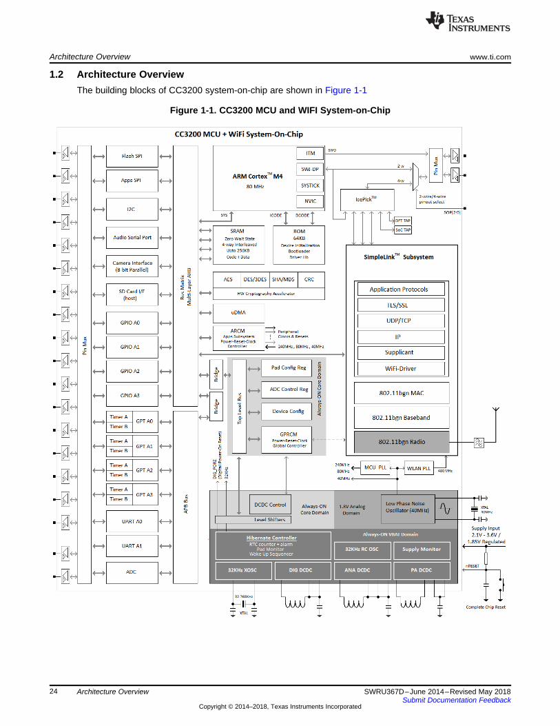
Architecture Overview www.ti.com
24 SWRU367D–June 2014–Revised May 2018Submit Documentation Feedback
Copyright © 2014–2018, Texas Instruments Incorporated
Architecture Overview
1.2 Architecture OverviewThe building blocks of CC3200 system-on-chip are shown in Figure 1-1
Figure 1-1. CC3200 MCU and WIFI System-on-Chip
www.ti.com Functional Overview
25SWRU367D–June 2014–Revised May 2018Submit Documentation Feedback
Copyright © 2014–2018, Texas Instruments Incorporated
Architecture Overview
1.3 Functional OverviewThe following sections provide an overview of the main components of the CC3200 system on chip (SoC)from a microcontroller point of view.
1.3.1 Processor Core
1.3.1.1 ARM CortexTM M4 Processor CoreThe CC3200 application MCU subsystem is built around an ARM Cortex-M4 processor core, whichprovides outstanding computational performance and exceptional system response to interrupts at lowpower consumption while optimizing memory footprint – making it an ideal fit for embedded applications.
Key features of ARM Cortex-M4 processor core are:• Thumb-2 mixed 16- and 32-bit instruction set delivers the high performance expected of a 32-bit ARM
core in a compact memory size – enabling richer applications within a given device memory size.• Single-cycle multiply instruction and hardware divide• Atomic bit manipulation (bit-banding), delivering maximum memory use and streamlined peripheral
control• Unaligned data access, enabling data to be efficiently packed into memory• Fast code execution, permitting slower processor clock or increased sleep mode time.• Hardware division and fast multiplier• Deterministic, high-performance interrupt handling for time-critical applications• Bit-band support for memory and select peripherals that includes atomic bit-band write and read
operations• Configurable 4-pin JTAG and 2-pin (SWJ-DP) debug access• Flash patch and breakpoint (FPB) unit to implement breakpoints and code patches• Ultra-low power sleep modes• Low active power consumption• 80-MHz operation
1.3.1.2 System Timer (SysTick)The ARM Cortex-M4 processor core includes an integrated system timer, SysTick. SysTick provides asimple, 24-bit, clear-on-write, decrementing, wrap-on-zero counter with a flexible control mechanism. Thecounter is clocked on the system clock.
SysTick makes OS porting between Cortex-M4 devices much easier because there is no need to changethe OS system timer code. The SysTick timer integrates with the NVIC and can generate a SysTickexception (exception type 15). In many OSes, a hardware timer generates interrupts so that the OS canperform task management (for example, to allow multiple tasks to run at different time slots and to ensurethat no single task can lock up the entire system). To perform this function, the timer must be able togenerate interrupts and, if possible, be protected from user tasks so that user applications cannot changethe timer behavior.
The counter can be used in several different ways; for example:• An RTOS tick timer that fires at a programmable rate (for example, 100 Hz) and invokes a SysTick
routine• A high-speed alarm timer using the system clock• A simple counter used to measure time to completion and time used• An internal clock-source control based on missing or meeting durations
Functional Overview www.ti.com
26 SWRU367D–June 2014–Revised May 2018Submit Documentation Feedback
Copyright © 2014–2018, Texas Instruments Incorporated
Architecture Overview
1.3.1.3 Nested Vector Interrupt Controller (NVIC)CC3200 includes the ARM NVIC. The NVIC and Cortex-M3 prioritize and handle all exceptions in handlermode. The processor state is automatically stored to the stack on an exception and automatically restoredfrom the stack at the end of the interrupt service routine (ISR). The interrupt vector is fetched in parallel tothe state saving, thus enabling efficient interrupt entry. The processor supports tail-chaining, meaning thatback-to-back interrupts can be performed without the overhead of state saving and restoration. The NVICand Cortex-M4 processor prioritize and handle all exceptions in handler mode. The NVIC and theprocessor core interface are closely coupled to enable low-latency interrupt processing and efficientprocessing of late-arriving interrupts. The NVIC maintains knowledge of the stacked, or nested, interruptsto enable tail-chaining of interrupts.
Key features are:• Exceptional interrupt handling through hardware implementation of required register manipulations• Deterministic, fast interrupt processing: always 12 cycles, or just 6 cycles with tail-chaining• Programmable priority level for each interrupt• Low-latency interrupt and exception handling• Level and pulse detection of interrupt signals• Grouping of interrupts into group priority and sub-priority interrupts• Tail chaining of interrupts
1.3.1.4 System Control BlockThe system control block (SCB) provides system implementation information and system control, includingconfiguration, control, and reporting of system exceptions.
1.3.2 Memory
1.3.2.1 On-Chip SRAMTo enable low-cost applications, the CC3200 device family follows a flash-less approach. CC3200 has upto 256KB of zero wait state, on-chip SRAM, to which application programs are downloaded and executed.The SRAM is used for both code and data, and is connected to the Multi-Layer-AHB bus-matrix of thechip. There is no restriction on relative size or partitioning of code and data.
The micro direct memory access (μDMA) controller can transfer data to and from SRAM and variousperipherals. The SRAM banks implement an advanced 4-way interleaved architecture which almosteliminates the performance penalty when DMA and processor simultaneously access the SRAM.
Internal RAM has selective retention capability during low-power deep-sleep (LPDS) mode. Based onneed, during LPDS mode the application can choose to retain 256KB, 192KB, 128KB or 64KB. Retainingthe memory during low power mode provides a faster wakeup. TI provides an easy to use powermanagement framework for processor and peripheral context save and restore mechanism based onSRAM retention. For more information, refer to the Power Management Framework User Guide inSection 15.6.
1.3.2.2 ROMCC3200 comes with factory programmed zero-wait-state ROM with the following firmware components:• Device initialization• Bootloader• Peripheral driver library (DriverLib) release for product-specific peripherals and interfaces
When CC3200 powers up, or chip reset is released or returns from hibernate mode, the deviceinitialization procedure is executed first. After the chip hardware has been correctly configured, thebootloader is executed, which loads the application code from non-volatile memory into on-chip SRAMand makes a jump to the application code entry point.
www.ti.com Functional Overview
27SWRU367D–June 2014–Revised May 2018Submit Documentation Feedback
Copyright © 2014–2018, Texas Instruments Incorporated
Architecture Overview
The CC3200 DriverLib is a software library that controls on-chip peripherals. The library performs bothperipheral initialization and control functions, with a choice of polled or interrupt-driven peripheral support.
The ROM DriverLib provides a rich set of drivers for peripheral and chip. It is aimed at reducingapplication development time and improving solution robustness. TI recommends that applications makeextensive use of the DriverLib APIs to optimize memory and MIPS requirement of end applications.
1.3.3 Micro Direct Memory Access Controller (µDMA)The CC3200 microcontroller includes a multichannel DMA controller, or μDMA. The μDMA controllerprovides a way to offload data-transfer tasks from the Cortex-M4 processor, allowing more efficient use ofthe processor and the available bus bandwidth. The μDMA controller can perform transfers betweenmemory and peripherals; it has dedicated channels for each supported on-chip module. The μDMAcontroller can be programmed to automatically perform transfers between peripherals and memory as theperipheral is ready to transfer more data.
The μDMA controller provides the following features:• 32 configurable channels• 80-MHz operation• Support for memory to memory, memory to peripheral, and peripheral to memory in multiple transfer
modes– Basic and simple transfer scenarios– Ping-Pong for continuous data flow– Scatter-gather for a programmable list of arbitrary transfers initiated from a single request
• Highly flexible and configurable channel operation– Independently configured and operated channels– Dedicated channels for supported on-chip modules– One channel each for receive and transmit path for bidirectional modules– Dedicated channel for software-initiated transfers– Per-channel configurable bus arbitration scheme– Software-initiated requests for any channel
• Two levels of priority• Design optimizations for improved bus access performance between the µDMA controller and the
processor core– µDMA controller access subordinate to core access– Simultaneous concurrent access
• Data sizes of 8, 16, and 32 bits• Transfer size is programmable in binary steps from 1 to 1024• Source and destination address increment size of byte, half-word, word, or no increment• Maskable peripheral requests• Interrupt on transfer completion, with a separate interrupt per channel
1.3.4 General Purpose Timer (GPT)The CC3200 includes 4 instances of 32-bit user-programmable general purpose timers. GPTs count ortime external events that drive the timer input pins. Each GPT module (GPTM) block provides two 16-bittimers or counters that can be configured to operate independently as timers or event counters, orconfigured to operate as one 32-bit timer. The GPTM contains GPTM blocks with the following functionaloptions:
• Operating modes:– 16- or 32-bit programmable one-shot timer– 16- or 32-bit programmable periodic timer
Functional Overview www.ti.com
28 SWRU367D–June 2014–Revised May 2018Submit Documentation Feedback
Copyright © 2014–2018, Texas Instruments Incorporated
Architecture Overview
– 16-bit general-purpose timer with an 8-bit prescaler– 16-bit input-edge count or time-capture modes– 16-bit pulse-width modulation (PWM) mode with software-programmable output inversion of the
PWM signal• Count up or down• Ability to determine the elapsed time between the assertion of the timer interrupt and entry into the ISR• Can trigger efficient transfers using the µDMA.
– Dedicated channel for each timer– Burst request generated on timer interrupt
1.3.5 Watch Dog Timer (WDT)The watchdog timer in the CC3200 restarts the system when it gets stuck due to an error and does notrespond as expected. The watchdog timer can be configured to generate an interrupt to themicrocontroller on its first time-out, and to generate a reset signal on its second time-out. Once thewatchdog timer is configured, the lock register can be written to prevent the timer configuration from beinginadvertently altered.
The watchdog timer provides the following features:• 32-bit down-counter with a programmable load register• Programmable interrupt generation logic with interrupt masking• Lock register protection from runaway software• Reset generation logic
1.3.6 Multi-Channel Audio Serial Port (McASP)CC3200 includes a configurable multichannel audio serial port for glue-less interfacing to audio CODECand DAC (speaker drivers). The audio port has two serializer / deserializers that can be individuallyenabled to either transmit or receive and operate synchronously. Key features are:• Two stereo I2S channels
– One stereo receive and one stereo transmit lines– Two stereo transmit lines
• Programmable clock and frame-sync polarity (rising or falling edge)• Programmable word length (bits per word): 16 and 24 bits• Programmable fractional divider for bit-clock generation, up to 9 MHz.
1.3.7 Serial Peripheral Interface (SPI)The serial peripheral interface (SPI) is a four-wire bidirectional communications interface that convertsdata between parallel and serial. The SPI module performs serial-to-parallel conversion on data receivedfrom a peripheral device, and parallel-to-serial conversion on data transmitted to a peripheral device. TheSPI allows a duplex serial communication between a local host and SPI-compliant external devices.
The CC3200 includes one SPI port dedicated to the application. Key features are• Programmable interface operation for Freescale SPI, MICROWIRE, or TI synchronous serial interfaces
master and slave modes• 3-pin and 4-pin mode• Full duplex and half duplex• Serial clock with programmable frequency, polarity, and phase• Up to 20-MHz operation• Programmable chip select polarity• Programmable delay before the first SPI word is transmitted• Programmable timing control between chip select and external clock generation
www.ti.com Functional Overview
29SWRU367D–June 2014–Revised May 2018Submit Documentation Feedback
Copyright © 2014–2018, Texas Instruments Incorporated
Architecture Overview
• No dead cycle between two successive words in slave mode• SPI word lengths of 8, 16, and 32 bits• Efficient transfers using the μDMA controller• Programmable interface operation for Freescale SPI, MICROWIRE, or TI-SSI
1.3.8 Inter-Integrated Circuit Interface (I2C)The inter-integrated circuit (I2C) bus provides bidirectional data transfer through a two-wire design (aserial data line SDA and a serial clock line SCL). The I2C bus interfaces to a wide variety of external I2Cdevices such as sensors, serial memory, control ports of image sensors, and audio codecs. Multiple slavedevices can be connected to the same I2C bus. The CC3200 microcontroller includes one I2C modulewith the following features:• Master and slave modes of operation• Master with arbitration and clock synchronization• Multi-master support• 7-bit addressing mode• Standard (100 Kbps) and fast (400 Kbps) modes
1.3.9 Universal Asynchronous Receiver/Transmitter (UART)A universal asynchronous receivers/transmitter (UART) is an integrated circuit used for RS-232 serialcommunications. UARTs contain a transmitter (parallel-to-serial converter) and a receiver (serial-to-parallel converter), each clocked separately.
The CC3200 device includes two fully programmable UARTs. The UART can generate individually-masked interrupts from the RX, TX, modem status, and error conditions. The module generates a singlecombined interrupt when any of the interrupts are asserted and unmasked.
The UARTs include the following features:• Programmable baud-rate generator, allowing speeds up to 3 Mbps• Separate 16 × 8 transmit (TX) and receive (RX) FIFOs to reduce CPU interrupt service loading• Programmable FIFO length, including 1-byte deep operation providing conventional double-buffered
interface• FIFO trigger levels of 1/8, 1/4, 1/2, 3/4, and 7/8• Standard asynchronous communication bits for start, stop, and parity• Line-break generation and detection• Fully programmable serial interface characteristics:
– 5, 6, 7, or 8 data bits– Even, odd, stick, or no-parity bit generation and detection– 1 or 2 stop-bit generation
• RTS and CTS modem handshake support• Standard FIFO-level and end-of-transmission interrupts• Efficient transfers using µDMA
– Separate channels for transmit and receive– Receive single request asserted when data is in the FIFO; burst request asserted at programmed
FIFO level– Transmit single request asserted when there is space in the FIFO; burst request asserted at
programmed FIFO level

Functional Overview www.ti.com
30 SWRU367D–June 2014–Revised May 2018Submit Documentation Feedback
Copyright © 2014–2018, Texas Instruments Incorporated
Architecture Overview
1.3.10 General Purpose Input / Output (GPIO)All digital pins of the CC3200 device and some of the analog pins can be used as a general-purposeinput/output (GPIO). The GPIOs are grouped as 4 instance GPIO modules, each 8-bit. Supported featuresinclude:• Up to 24 GPIOs, depending on the functional pin configuration• Interrupt capability for all GPIO pins
– Level or edge sensitive– Rising or falling edge– Selective interrupt masking
• Can trigger DMA operation• Selectable wakeup source (one out of 6 pins)• Programmable pad configuration
– Internal 5 µA pull-up and pull-down– Configurable drive strength of 2, 4, 6, 8, 10, 12, and 14 mA– Open-drain mode
• GPIO register readable through the high-speed internal bus matrix
1.3.11 Analog to Digital Converter (ADC)The ADC peripheral converts a continuous analog voltage into a discrete digital number. The CC3200device includes ADC modules with four input channels. Each ADC module features 12-bit conversionresolution for the four input channels. Features include:• Number of bits: 12-bit• Effective nominal accuracy: 10 bits• Four analog input channels• Automatic round-robin sampling• Fixed sampling interval of 16 µs per channel• Automatic 16-bit time-stamping of every ADC samples based on the system clock• Dedicated DMA channel to transfer ADC channel data to the application RAM.
1.3.12 SD Card HostThe CC3200 includes an SD-Host interface for applications that require mass storage. The SD-Hostinterface support is limited to 1-bit mode due to chip pin constraints.
1.3.13 Parallel Camera InterfaceThe CC3200 includes an 8-bit parallel camera port to enable image sensor-based applications.
1.3.14 Debug InterfaceThe CC3200 supports both IEEE Standard 1149.1 JTAG (4-wire) and the low-pin-count ARM SWD (2-wire) debug interfaces. Depending on the board level configuration of the sense-on-power pull resistors,by default the chip powers up with either the 4-wire JTAG or the 2-wire SWD interface.
As shown in Figure 1-1, the 4-wire JTAG signals from the chip pins are routed through an IcePick module.TAPs other than the application MCU are reserved for TI production testing. A TAP select sequence mustbe sent to the device to connect to the ARM Cortex M4 JTAG TAP. The 2-wire mode, however, directlyroutes the ARM SWD-TMS and SWD-TCK pins directly to the respective chip pins.
www.ti.com Functional Overview
31SWRU367D–June 2014–Revised May 2018Submit Documentation Feedback
Copyright © 2014–2018, Texas Instruments Incorporated
Architecture Overview
1.3.15 Hardware Cryptography AcceleratorThe secure variant of the CC3200 includes a suite of high-throughput, state-of-the-art hardwareaccelerators for fast computation of ciphers (AES, DES, 3-DES), hashing (SHA, MD5), and CRCalgorithms by the application. It is also referred as the data hashing and transform engine (DTHE). Furtherdetails about the hardware cryptography accelerator will be addressed in the revision of this manual.
NOTE: Present production devices have the Crypto unlocked (Fuse Farm); a user application canuse these.
NOTE: Secure MCU ensures secure booting of the user application using the crypto engines. Thisfeature will be available in future revisions of the device.
1.3.16 Clock, Reset, and Power ManagementThe CC3200 system-on-chip includes the necessary clock and power management functionalities to builda standalone battery-operated low power solution. Key features are:• Primary clocks
– Slow clock: 32.768 KHz (+/-250 ppm)• Used in RTC, Wi-Fi beacon listen timing in low power IDLE mode and some of the chip internal
sequencing• On-chip, low power 32-KHz Xtal oscillator• Support for externally-fed 32.768 KHz clock• On-chip 32-KHz RC oscillator for initial wakeup
– Fast clock: 40 MHz (+/-20 ppm)• Used in Wi-Fi radio and MCU.• On-chip low phase-noise 40-MHz Xtal oscillator• Support for externally-fed clean 40 MHz clock (such as TCXO)• System and peripheral clocks are derived from internal PLL producing 240 MHz
• Flexible reset scheme– The following resets are supported in CC3200
• External chip reset pin: the entire chip, including power management, is reset when thenRESET pin is held low.
• Reset on hibernate: the entire core is reset when the chip goes through a hibernate cycle.• Reset on watchdog: the application MCU is reset when the watchdog timer expires.• Soft-reset: the application MCU is reset by software
– Complete system recovery from any stuck-at scenario can be achieved by using a combination ofWDT reset and hibernate sleep.
• On-chip power management– The CC3200 supports two supply configurations:
• Wide voltage mode: 2.1 V to 3.6 V• Powered by battery (2×1.5 V) or a regulated 3.3-V supply.
• Regulated 1.85 V• For applications with on-board DCDC regulator
– A set of 3 on-chip high-efficiency DCDC converters produce the internal module supply voltageswhen they are needed. These switching converters and their frequency plan are optimized tominimize interference to WLAN radio.• DIG-DCDC: Produces 0.9 V to 1.2 V for the core digital logic• ANA1-DCDC: Produces low-ripple 1.8-V supply for the analog and RF. This is bypassed in the
Functional Overview www.ti.com
32 SWRU367D–June 2014–Revised May 2018Submit Documentation Feedback
Copyright © 2014–2018, Texas Instruments Incorporated
Architecture Overview
regulated 1.85-V configuration.• PA-DCDC: Produces regulated 1.8 V with extremely fast transient regulation for the WLAN RF
Transmit Power Amplifier. This is bypassed in the regulated 1.85-V configuration.– A set of low dropout regulators (LDOs) are used in the radio subsystem to further regulate and filter
the ANA1-DCDC output before being fed to the analog circuits.– On-chip factory-trimmed accurate band-gap voltage reference ensures the regulator outputs are
stable across process and temperature.
1.3.17 SimpleLink SubsystemThe SimpleLink subsystem provides fast, secured WLAN and Internet connections with 256-bit encryption.The CC3200 device supports station, AP, and Wi-Fi Direct modes. The device also supports WPA2personal and enterprise security and WPS 2.0. The Wi-Fi network processor includes an embedded IPv4TCP/IP stack.
This multi-processor subsystem consists of the following:• IPv4 network processor and Wi-Fi driver• 802.11 b/g/n MAC• 802.11 b/g/n PHY• 802.11 b/g/n Radio
The SimpleLink subsystem is accessible from the application MCU over an asynchronous link, and can becontrolled through a complete set of SimpleLink host driver APIs provided as part of the ROM driverlibrary. The mode of usage is similar to that of an external MCU using the CC3100 device.
The co-location of the Wi-Fi subsystem on the same die imposes a few restrictions on the applicationMCU. These will be covered in detail in Chapter 15.
1.3.18 I/O Pads and Pin MultiplexingThe device makes extensive use of pin multiplexing to accommodate the large number of peripheralfunctions in the smallest possible package. To achieve this configuration, pin multiplexing is controlledusing a combination of hardware configuration (at device reset) and register control.
The I/O pad and pin mux sections feature flexible wide-voltage I/Os. Supported features include:• Programmable drive strength from 2 mA to 14 mA (nominal condition) in steps of 2 mA.• Open drain mode• Output buffer isolation• Automatic output isolation during reset and hibernate• Configurable pull-up and pull-down (10 µA nominal)• Software-configurable pad state retention during LPDS• All digital I/Os are nonfail-safe.
33SWRU367D–June 2014–Revised May 2018Submit Documentation Feedback
Copyright © 2014–2018, Texas Instruments Incorporated
Cortex-M4 Processor
Chapter 2SWRU367D–June 2014–Revised May 2018
Cortex-M4 Processor
Topic ........................................................................................................................... Page
2.1 Overview ........................................................................................................... 342.2 Functional Description........................................................................................ 36
Overview www.ti.com
34 SWRU367D–June 2014–Revised May 2018Submit Documentation Feedback
Copyright © 2014–2018, Texas Instruments Incorporated
Cortex-M4 Processor
2.1 OverviewThe CC3200 incorporates a dedicated instance of the ARM Cortex-M4 CPU core for executing applicationcode with or without RTOS. This processor core is not used in any manner for running any networking ordevice management task.
This dedicated ARM Cortex-M4 core, along with large on-chip SRAM, a rich set of peripherals, andadvanced DC-DC-based power management, provides a robust, contention-free, high-performanceapplication platform at much lower power, lower cost, and smaller solution size when compared tosolutions based on discrete MCUs.
Features include:• 32-bit ARM Cortex-M4 architecture optimized for small-footprint embedded applications• 80-MHz operation• Fast interrupt handling• Thumb-2 mixed 16-/32-bit instruction set delivers the high performance expected of a 32-bit ARM core
in a compact memory size usually associated with 8- and 16-bit devices, typically in the range of a fewkilobytes of memory for microcontroller-class applications.– Single-cycle multiply instruction and hardware divide– Atomic bit manipulation (bit-banding), delivering maximum memory utilization and streamlined
peripheral control– Unaligned data access, enabling data to be efficiently packed into memory
• 16-bit SIMD vector processing unit• 3-stage pipeline Harvard architecture• Hardware division and fast digital-signal-processing orientated multiply accumulate• Saturating arithmetic for signal processing• Deterministic, high-performance interrupt handling for time-critical applications• Enhanced system debug with extensive breakpoints• Serial-wire debug and serial-wire trace reduce the number of pins required for debugging and tracing• Low-power consumption with multiple sleep modes
The ARM Cortex-M4 application processor core in the CC3200 does not include the floating point unit andmemory protection unit (FPU and MPU).
This chapter provides information on the implementation of the Cortex-M4 application processor in theCC3200, including the programming model, the memory model, the exception model, fault handling, andpower management.
For technical details on the instruction set, see the Cortex-M4 instruction set chapter in the ARM®Cortex™-M4 Devices Generic User Guide (ARM DUI 0553A).
2.1.1 Block DiagramThe block diagram is shown in Figure 2-1.
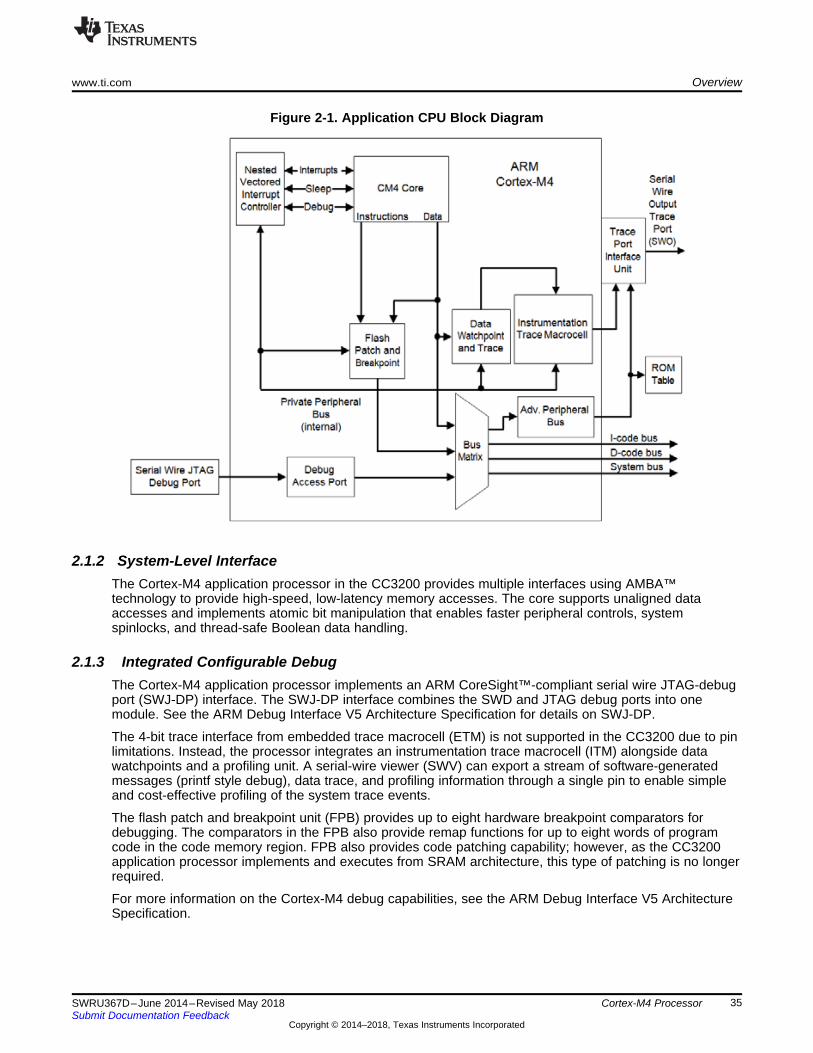
www.ti.com Overview
35SWRU367D–June 2014–Revised May 2018Submit Documentation Feedback
Copyright © 2014–2018, Texas Instruments Incorporated
Cortex-M4 Processor
Figure 2-1. Application CPU Block Diagram
2.1.2 System-Level InterfaceThe Cortex-M4 application processor in the CC3200 provides multiple interfaces using AMBA™technology to provide high-speed, low-latency memory accesses. The core supports unaligned dataaccesses and implements atomic bit manipulation that enables faster peripheral controls, systemspinlocks, and thread-safe Boolean data handling.
2.1.3 Integrated Configurable DebugThe Cortex-M4 application processor implements an ARM CoreSight™-compliant serial wire JTAG-debugport (SWJ-DP) interface. The SWJ-DP interface combines the SWD and JTAG debug ports into onemodule. See the ARM Debug Interface V5 Architecture Specification for details on SWJ-DP.
The 4-bit trace interface from embedded trace macrocell (ETM) is not supported in the CC3200 due to pinlimitations. Instead, the processor integrates an instrumentation trace macrocell (ITM) alongside datawatchpoints and a profiling unit. A serial-wire viewer (SWV) can export a stream of software-generatedmessages (printf style debug), data trace, and profiling information through a single pin to enable simpleand cost-effective profiling of the system trace events.
The flash patch and breakpoint unit (FPB) provides up to eight hardware breakpoint comparators fordebugging. The comparators in the FPB also provide remap functions for up to eight words of programcode in the code memory region. FPB also provides code patching capability; however, as the CC3200application processor implements and executes from SRAM architecture, this type of patching is no longerrequired.
For more information on the Cortex-M4 debug capabilities, see the ARM Debug Interface V5 ArchitectureSpecification.
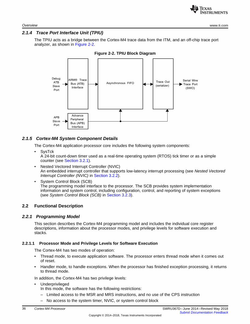
Debug
ATB
Slave
Port
ARM® Trace
Bus (ATB)
Interface
Asynchronous FIFO Trace Out
(serializer)
Serial Wire
Trace Port
(SWO)
APB
Slave
Port
Advance
Peripheral
Bus (APB)
Interface
Overview www.ti.com
36 SWRU367D–June 2014–Revised May 2018Submit Documentation Feedback
Copyright © 2014–2018, Texas Instruments Incorporated
Cortex-M4 Processor
2.1.4 Trace Port Interface Unit (TPIU)The TPIU acts as a bridge between the Cortex-M4 trace data from the ITM, and an off-chip trace portanalyzer, as shown in Figure 2-2.
Figure 2-2. TPIU Block Diagram
2.1.5 Cortex-M4 System Component DetailsThe Cortex-M4 application processor core includes the following system components:• SysTck
A 24-bit count-down timer used as a real-time operating system (RTOS) tick timer or as a simplecounter (see Section 3.2.1).
• Nested Vectored Interrupt Controller (NVIC)An embedded interrupt controller that supports low-latency interrupt processing (see Nested VectoredInterrupt Controller (NVIC) in Section 3.2.2).
• System Control Block (SCB)The programming model interface to the processor. The SCB provides system implementationinformation and system control, including configuration, control, and reporting of system exceptions(see System Control Block (SCB) in Section 3.2.3).
2.2 Functional Description
2.2.1 Programming ModelThis section describes the Cortex-M4 programming model and includes the individual core registerdescriptions, information about the processor modes, and privilege levels for software execution andstacks.
2.2.1.1 Processor Mode and Privilege Levels for Software ExecutionThe Cortex-M4 has two modes of operation:• Thread mode, to execute application software. The processor enters thread mode when it comes out
of reset.• Handler mode, to handle exceptions. When the processor has finished exception processing, it returns
to thread mode.
In addition, the Cortex-M4 has two privilege levels:• Underprivileged
In this mode, the software has the following restrictions:– Limited access to the MSR and MRS instructions, and no use of the CPS instruction– No access to the system timer, NVIC, or system control block
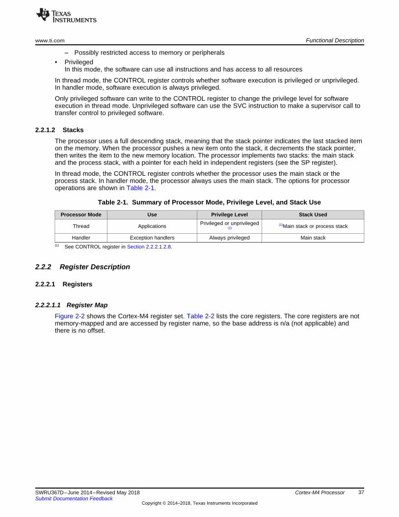
www.ti.com Functional Description
37SWRU367D–June 2014–Revised May 2018Submit Documentation Feedback
Copyright © 2014–2018, Texas Instruments Incorporated
Cortex-M4 Processor
– Possibly restricted access to memory or peripherals• Privileged
In this mode, the software can use all instructions and has access to all resources
In thread mode, the CONTROL register controls whether software execution is privileged or unprivileged.In handler mode, software execution is always privileged.
Only privileged software can write to the CONTROL register to change the privilege level for softwareexecution in thread mode. Unprivileged software can use the SVC instruction to make a supervisor call totransfer control to privileged software.
2.2.1.2 StacksThe processor uses a full descending stack, meaning that the stack pointer indicates the last stacked itemon the memory. When the processor pushes a new item onto the stack, it decrements the stack pointer,then writes the item to the new memory location. The processor implements two stacks: the main stackand the process stack, with a pointer for each held in independent registers (see the SP register).
In thread mode, the CONTROL register controls whether the processor uses the main stack or theprocess stack. In handler mode, the processor always uses the main stack. The options for processoroperations are shown in Table 2-1.
(1) See CONTROL register in Section 2.2.2.1.2.8.
Table 2-1. Summary of Processor Mode, Privilege Level, and Stack Use
Processor Mode Use Privilege Level Stack Used
Thread Applications Privileged or unprivileged(1)
(1)Main stack or process stack
Handler Exception handlers Always privileged Main stack
2.2.2 Register Description
2.2.2.1 Registers
2.2.2.1.1 Register MapFigure 2-2 shows the Cortex-M4 register set. Table 2-2 lists the core registers. The core registers are notmemory-mapped and are accessed by register name, so the base address is n/a (not applicable) andthere is no offset.
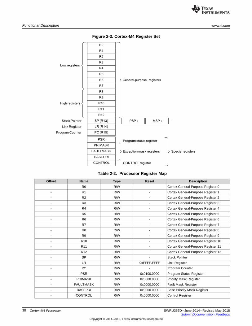
Functional Description www.ti.com
38 SWRU367D–June 2014–Revised May 2018Submit Documentation Feedback
Copyright © 2014–2018, Texas Instruments Incorporated
Cortex-M4 Processor
Figure 2-3. Cortex-M4 Register Set
Table 2-2. Processor Register Map
Offset Name Type Reset Description- R0 R/W - Cortex General-Purpose Register 0- R1 R/W - Cortex General-Purpose Register 1- R2 R/W - Cortex General-Purpose Register 2- R3 R/W - Cortex General-Purpose Register 3- R4 R/W - Cortex General-Purpose Register 4- R5 R/W - Cortex General-Purpose Register 5- R6 R/W - Cortex General-Purpose Register 6- R7 R/W - Cortex General-Purpose Register 7- R8 R/W - Cortex General-Purpose Register 8- R9 R/W - Cortex General-Purpose Register 9- R10 R/W - Cortex General-Purpose Register 10- R11 R/W - Cortex General-Purpose Register 11- R12 R/W - Cortex General-Purpose Register 12- SP R/W - Stack Pointer- LR R/W 0xFFFF.FFFF Link Register- PC R/W - Program Counter- PSR R/W 0x0100.0000 Program Status Register- PRIMASK R/W 0x0000.0000 Priority Mask Register- FAULTMASK R/W 0x0000.0000 Fault Mask Register- BASEPRI R/W 0x0000.0000 Base Priority Mask Register- CONTROL R/W 0x0000.0000 Control Register
www.ti.com Functional Description
39SWRU367D–June 2014–Revised May 2018Submit Documentation Feedback
Copyright © 2014–2018, Texas Instruments Incorporated
Cortex-M4 Processor
Table 2-2. Processor Register Map (continued)Offset Name Type Reset Description
- FPSC R/W - Floating-Point Status Control (N/A forCC3200)
2.2.2.1.2 Register DescriptionsThis section lists and describes the Cortex-M4 registers. The core registers are not memory-mapped, andare accessed by register name rather than offset.
NOTE: The register type shown in the register descriptions refers to type during program executionin thread mode and handler mode. Debug access may differ.
The Rn registers are 32-bit general-purpose registers for data operations, and can be accessed fromeither privileged or unprivileged mode.
2.2.2.1.2.1 Stack Pointer (SP)In thread mode, the function of this register changes depending on the ASP bit in the Control Register(CONTROL) register. When the ASP bit is clear, this register is the main stack pointer (MSP). When theASP bit is set, this register is the process stack pointer (PSP). On reset, the ASP bit is clear, and theprocessor loads the MSP with the value from address 0x0000 0000. The MSP can only be accessed inprivileged mode; the PSP can be accessed in either privileged or unprivileged mode.
2.2.2.1.2.2 Link Register (LR)The Link register (LR) stores the return information for subroutines, function calls, and exceptions. TheLink register can be accessed from either privileged or unprivileged mode.
EXC_RETURN is loaded into the LR on exception entry.
2.2.2.1.2.3 Program Counter (PC)The program counter (PC) contains the current program address. On reset, the processor loads the PCwith the value of the reset vector, which is at address 0x0000 0004. Bit 0 of the reset vector is loaded intothe THUMB bit of the EPSR at reset and must be 1. The PC register can be accessed in either privilegedor unprivileged mode.
2.2.2.1.2.4 Program Status Register (PSR)
NOTE: This register is also referred to as xPSR.
The Program Status (PSR) register has three functions, and the register bits are assigned to the differentfunctions:• Application Program Status (APSR) register, bits 31:27, bits 19:16• Execution Program Status (EPSR) register, bits 26:24, 15:10• Interrupt Program Status (IPSR) register, bits 7:0
The PSR, IPSR, and EPSR registers can only be accessed in privileged mode; the APSR register can beaccessed in either privileged or unprivileged mode.
APSR contains the current state of the condition flags from previous instruction executions. EPSRcontains the Thumb state bit and the execution state bits for the if-then (IT) instruction or the interruptible-continuable instruction (ICI) field for an interrupted load multiple or store multiple instruction. Attempts toread the EPSR directly through application software using the MSR instruction always return zero.Attempts to write the EPSR using the MSR instruction in application software are always ignored. Faulthandlers can examine the EPSR value in the stacked PSR to determine the operation that faulted.

Functional Description www.ti.com
40 SWRU367D–June 2014–Revised May 2018Submit Documentation Feedback
Copyright © 2014–2018, Texas Instruments Incorporated
Cortex-M4 Processor
IPSR contains the exception type number of the current interrupt service routine (ISR).
These registers can be accessed individually, or as a combination of any two or all three registers, usingthe register name as an argument to the MSR or MRS instructions. For example, all of the registers canbe read using PSR with the MRS instruction, or APSR only can be written to using APSR with the MSRinstruction. Table 2-3 shows the possible register combinations for the PSR. See the MRS and MSRinstruction descriptions in the Cortex-M4 instruction set chapter in the ARM Cortex-M4 Devices GenericUser Guide (ARM DUI 0553A) for more information about how to access the program status registers.
(1) The processor ignores writes to the IPSR bits.(2) Reads of the EPSR bits return zero, and the processor ignores writes to these bits
Table 2-3. PSR Register Combinations
Register Type CombinationPSR PSR R/W (1) (2) APSR, EPSR, and IPSR
IEPSR RO EPSR and IPSRIAPSR R/W (1) APSR and IPSREAPSR R/W (2) APSR and EPSR
2.2.2.1.2.5 Priority Mask Register (PRIMASK)The PRIMASK register prevents activation of all exceptions with programmable priority. Reset, non-maskable interrupt (NMI), and hard fault are the only exceptions with fixed priority. Exceptions should bedisabled when they might impact the timing of critical tasks. This register is only accessible in privilegedmode. The MSR and MRS instructions are used to access the PRIMASK register, and the CPS instructionmay be used to change the value of the PRIMASK register. See the Cortex-M4 instruction set chapter inthe ARM Cortex-M4 Devices Generic User Guide (ARM DUI 0553A) for more information on theseinstructions.
2.2.2.1.2.6 Fault Mask Register (FAULTMASK)The FAULTMASK register prevents activation of all exceptions except for the Non-Maskable Interrupt(NMI). Exceptions should be disabled when they might impact the timing of critical tasks. This register isonly accessible in privileged mode. The MSR and MRS instructions are used to access the FAULTMASKregister, and the CPS instruction may be used to change the value of the FAULTMASK register. See theCortex™-M4 instruction set chapter in the ARM® Cortex™-M4 Devices Generic User Guide (ARM DUI0553A) for more information on these instructions.
2.2.2.1.2.7 Base Priority Mask Register (BASEPRI)The BASEPRI register defines the minimum priority for exception processing. When BASEPRI is set to anonzero value, it prevents the activation of all exceptions with the same or lower priority level as theBASEPRI value. Exceptions should be disabled when they might impact the timing of critical tasks. Thisregister is only accessible in privileged mode.
2.2.2.1.2.8 Control Register (CONTROL)The CONTROL register controls the stack used and the privilege level for software execution when theprocessor is in thread mode, and indicates whether the FPU state is active. This register is only accessiblein privileged mode.
Handler mode always uses the MSP, so the processor ignores explicit writes to the ASP bit of theCONTROL register when in handler mode. The exception entry and return mechanisms automaticallyupdate the CONTROL register based on the EXC_RETURN value. In an OS environment, threads runningin thread mode should use the process stack, and the kernel and exception handlers should use the mainstack. By default, thread mode uses the MSP. To switch the stack pointer used in thread mode to thePSP, either use the MSR instruction to set the ASP bit, as detailed in the Cortex-M4 instruction setchapter in the ARM Cortex-M4 Devices Generic User Guide (ARM DUI 0553A), or perform an exceptionreturn to thread mode with the appropriate EXC_RETURN value.
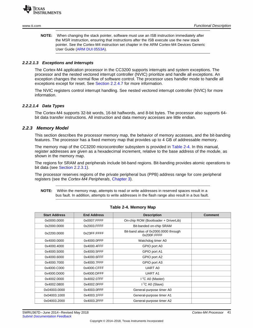
www.ti.com Functional Description
41SWRU367D–June 2014–Revised May 2018Submit Documentation Feedback
Copyright © 2014–2018, Texas Instruments Incorporated
Cortex-M4 Processor
NOTE: When changing the stack pointer, software must use an ISB instruction immediately afterthe MSR instruction, ensuring that instructions after the ISB execute use the new stackpointer. See the Cortex-M4 instruction set chapter in the ARM Cortex-M4 Devices GenericUser Guide (ARM DUI 0553A).
2.2.2.1.3 Exceptions and InterruptsThe Cortex-M4 application processor in the CC3200 supports interrupts and system exceptions. Theprocessor and the nested vectored interrupt controller (NVIC) prioritize and handle all exceptions. Anexception changes the normal flow of software control. The processor uses handler mode to handle allexceptions except for reset. See Section 2.2.4.7 for more information.
The NVIC registers control interrupt handling. See nested vectored interrupt controller (NVIC) for moreinformation.
2.2.2.1.4 Data TypesThe Cortex-M4 supports 32-bit words, 16-bit halfwords, and 8-bit bytes. The processor also supports 64-bit data transfer instructions. All instruction and data memory accesses are little endian.
2.2.3 Memory ModelThis section describes the processor memory map, the behavior of memory accesses, and the bit-bandingfeatures. The processor has a fixed memory map that provides up to 4 GB of addressable memory.
The memory map of the CC3200 microcontroller subsystem is provided in Table 2-4. In this manual,register addresses are given as a hexadecimal increment, relative to the base address of the module, asshown in the memory map.
The regions for SRAM and peripherals include bit-band regions. Bit-banding provides atomic operations tobit data (see Section 2.2.3.1).
The processor reserves regions of the private peripheral bus (PPB) address range for core peripheralregisters (see the Cortex-M4 Peripherals, Chapter 3).
NOTE: Within the memory map, attempts to read or write addresses in reserved spaces result in abus fault. In addition, attempts to write addresses in the flash range also result in a bus fault.
Table 2-4. Memory Map
Start Address End Address Description Comment0x0000.0000 0x0007.FFFF On-chip ROM (Bootloader + DriverLib)0x2000.0000 0x2003.FFFF Bit-banded on-chip SRAM
0x2200.0000 0x23FF.FFFF Bit-band alias of 0x2000.0000 through0x200F.FFFF
0x4000.0000 0x4000.0FFF Watchdog timer A00x4000.4000 0x4000.4FFF GPIO port A00x4000.5000 0x4000.5FFF GPIO port A10x4000.6000 0x4000.6FFF GPIO port A20x4000.7000 0x4000.7FFF GPIO port A30x4000.C000 0x4000.CFFF UART A00x4000.D000 0x4000.DFFF UART A10x4002.0000 0x4002.07FF I 2C A0 (Master)0x4002.0800 0x4002.0FFF I 2C A0 (Slave)0x04003.0000 0x4003.0FFF General-purpose timer A00x04003.1000 0x4003.1FFF General-purpose timer A10x04003.2000 0x4003.2FFF General-purpose timer A2
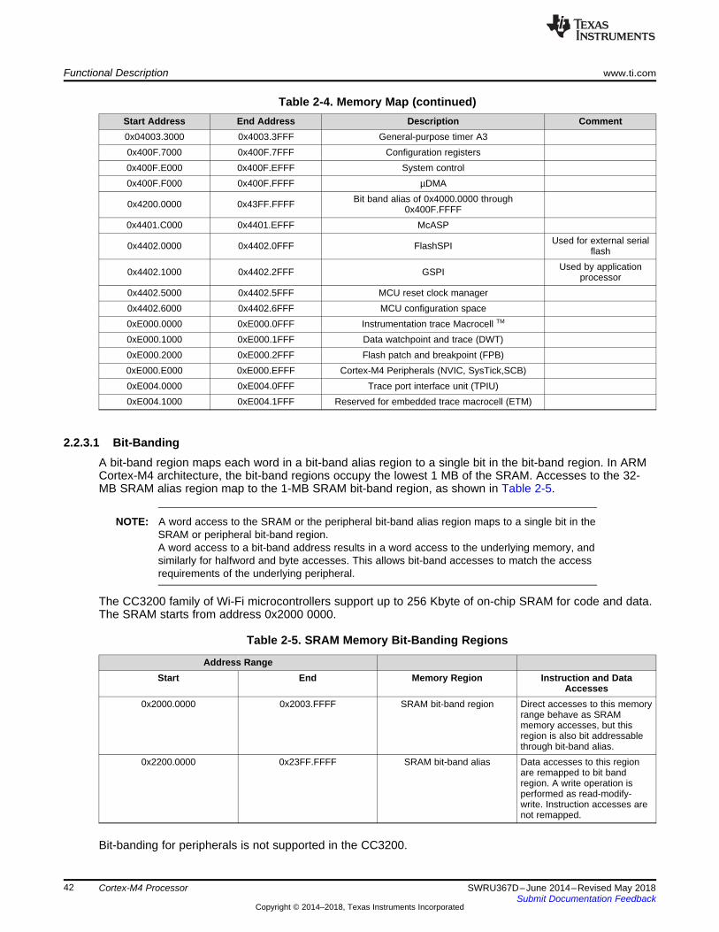
Functional Description www.ti.com
42 SWRU367D–June 2014–Revised May 2018Submit Documentation Feedback
Copyright © 2014–2018, Texas Instruments Incorporated
Cortex-M4 Processor
Table 2-4. Memory Map (continued)Start Address End Address Description Comment0x04003.3000 0x4003.3FFF General-purpose timer A30x400F.7000 0x400F.7FFF Configuration registers0x400F.E000 0x400F.EFFF System control0x400F.F000 0x400F.FFFF µDMA
0x4200.0000 0x43FF.FFFF Bit band alias of 0x4000.0000 through0x400F.FFFF
0x4401.C000 0x4401.EFFF McASP
0x4402.0000 0x4402.0FFF FlashSPI Used for external serialflash
0x4402.1000 0x4402.2FFF GSPI Used by applicationprocessor
0x4402.5000 0x4402.5FFF MCU reset clock manager0x4402.6000 0x4402.6FFF MCU configuration space0xE000.0000 0xE000.0FFF Instrumentation trace Macrocell TM
0xE000.1000 0xE000.1FFF Data watchpoint and trace (DWT)0xE000.2000 0xE000.2FFF Flash patch and breakpoint (FPB)0xE000.E000 0xE000.EFFF Cortex-M4 Peripherals (NVIC, SysTick,SCB)0xE004.0000 0xE004.0FFF Trace port interface unit (TPIU)0xE004.1000 0xE004.1FFF Reserved for embedded trace macrocell (ETM)
2.2.3.1 Bit-BandingA bit-band region maps each word in a bit-band alias region to a single bit in the bit-band region. In ARMCortex-M4 architecture, the bit-band regions occupy the lowest 1 MB of the SRAM. Accesses to the 32-MB SRAM alias region map to the 1-MB SRAM bit-band region, as shown in Table 2-5.
NOTE: A word access to the SRAM or the peripheral bit-band alias region maps to a single bit in theSRAM or peripheral bit-band region.A word access to a bit-band address results in a word access to the underlying memory, andsimilarly for halfword and byte accesses. This allows bit-band accesses to match the accessrequirements of the underlying peripheral.
The CC3200 family of Wi-Fi microcontrollers support up to 256 Kbyte of on-chip SRAM for code and data.The SRAM starts from address 0x2000 0000.
Table 2-5. SRAM Memory Bit-Banding Regions
Address RangeStart End Memory Region Instruction and Data
Accesses0x2000.0000 0x2003.FFFF SRAM bit-band region Direct accesses to this memory
range behave as SRAMmemory accesses, but thisregion is also bit addressablethrough bit-band alias.
0x2200.0000 0x23FF.FFFF SRAM bit-band alias Data accesses to this regionare remapped to bit bandregion. A write operation isperformed as read-modify-write. Instruction accesses arenot remapped.
Bit-banding for peripherals is not supported in the CC3200.
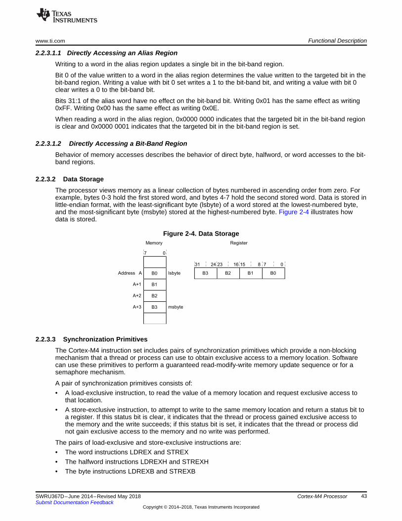
7 0
B0
B1
B2
B3
31 24 23 16 15 8 7 0
B3 B2 B1 B0
Memory Register
Address A
A+1
lsbyte
A+2
A+3 msbyte
www.ti.com Functional Description
43SWRU367D–June 2014–Revised May 2018Submit Documentation Feedback
Copyright © 2014–2018, Texas Instruments Incorporated
Cortex-M4 Processor
2.2.3.1.1 Directly Accessing an Alias RegionWriting to a word in the alias region updates a single bit in the bit-band region.
Bit 0 of the value written to a word in the alias region determines the value written to the targeted bit in thebit-band region. Writing a value with bit 0 set writes a 1 to the bit-band bit, and writing a value with bit 0clear writes a 0 to the bit-band bit.
Bits 31:1 of the alias word have no effect on the bit-band bit. Writing 0x01 has the same effect as writing0xFF. Writing 0x00 has the same effect as writing 0x0E.
When reading a word in the alias region, 0x0000 0000 indicates that the targeted bit in the bit-band regionis clear and 0x0000 0001 indicates that the targeted bit in the bit-band region is set.
2.2.3.1.2 Directly Accessing a Bit-Band RegionBehavior of memory accesses describes the behavior of direct byte, halfword, or word accesses to the bit-band regions.
2.2.3.2 Data StorageThe processor views memory as a linear collection of bytes numbered in ascending order from zero. Forexample, bytes 0-3 hold the first stored word, and bytes 4-7 hold the second stored word. Data is stored inlittle-endian format, with the least-significant byte (lsbyte) of a word stored at the lowest-numbered byte,and the most-significant byte (msbyte) stored at the highest-numbered byte. Figure 2-4 illustrates howdata is stored.
Figure 2-4. Data Storage
2.2.3.3 Synchronization PrimitivesThe Cortex-M4 instruction set includes pairs of synchronization primitives which provide a non-blockingmechanism that a thread or process can use to obtain exclusive access to a memory location. Softwarecan use these primitives to perform a guaranteed read-modify-write memory update sequence or for asemaphore mechanism.
A pair of synchronization primitives consists of:• A load-exclusive instruction, to read the value of a memory location and request exclusive access to
that location.• A store-exclusive instruction, to attempt to write to the same memory location and return a status bit to
a register. If this status bit is clear, it indicates that the thread or process gained exclusive access tothe memory and the write succeeds; if this status bit is set, it indicates that the thread or process didnot gain exclusive access to the memory and no write was performed.
The pairs of load-exclusive and store-exclusive instructions are:• The word instructions LDREX and STREX• The halfword instructions LDREXH and STREXH• The byte instructions LDREXB and STREXB
Functional Description www.ti.com
44 SWRU367D–June 2014–Revised May 2018Submit Documentation Feedback
Copyright © 2014–2018, Texas Instruments Incorporated
Cortex-M4 Processor
Software must use a load-exclusive instruction with the corresponding store-exclusive instruction. Toperform an exclusive read-modify-write of a memory location, software must:1. Use a load-exclusive instruction to read the value of the location.2. Modify the value, as required.3. Use a store-exclusive instruction to attempt to write the new value back to the memory location.4. Test the returned status bit. If the status bit is clear, the read-modify-write completed successfully. If
the status bit is set, no write was performed, which indicates that the value returned at Step 1 might beout of date. The software must retry the entire read-modify-write sequence.
Software can use the synchronization primitives to implement a semaphore as follows:1. Use a load-exclusive instruction to read from the semaphore address, to check whether the semaphore
is free.2. If the semaphore is free, use a store-exclusive to write the claim value to the semaphore address.3. If the returned status bit from Step 2 indicates that the store-exclusive succeeded, then the software
has claimed the semaphore. However, if the store-exclusive failed, another process might haveclaimed the semaphore after the software performed Step 1.
The Cortex-M4 includes an exclusive access monitor that tags the fact that the processor has executed aload-exclusive instruction. The processor removes its exclusive access tag if:• It executes a CLREX instruction.• It executes a store-exclusive instruction, regardless of whether the write succeeds.• An exception occurs, which means the processor can resolve semaphore conflicts between different
threads.
For more information about the synchronization primitive instructions, see the Cortex-M4 instruction setchapter in the ARM Cortex-M4 Devices Generic User Guide (ARM DUI 0553A).
2.2.4 Exception ModelThe ARM Cortex-M4 application processor in the CC3200 and the nested vectored interrupt controller(NVIC) prioritize and handle all exceptions in handler mode. The processor state is automatically stored tothe stack on an exception, and automatically restored from the stack at the end of the interrupt serviceroutine (ISR). The vector is fetched in parallel to the state saving, enabling efficient interrupt entry. Theprocessor supports tail-chaining, which enables back-to-back interrupts to be performed without theoverhead of state saving and restoration.
Table 2-6 lists all exception types. Software can set eight priority levels on seven of these exceptions(system handlers) as well as on 70 interrupts (listed in Table 2-6). Priorities on the system handlers areset with the NVIC System Handler Priority n (SYSPRIn) registers. Interrupts are enabled through the NVICInterrupt Set Enable n (ENn) register and prioritized with the NVIC Interrupt Priority n (PRIn) registers.Priorities can be grouped by splitting priority levels into preemption priorities and subpriorities. All theinterrupt registers are described in Section 3.2.2.
Internally, the highest user-programmable priority (0) is treated as fourth priority, after a reset, non-maskable interrupt (NMI), and a hard fault, in that order. Note that 0 is the default priority for all theprogrammable priorities.
NOTE: After a write to clear an interrupt source, it may take several processor cycles for the NVIC tosee the interrupt source de-assert. Thus, if the interrupt clear is done as the last action in aninterrupt handler, it is possible for the interrupt handler to complete while the NVIC sees theinterrupt as still asserted, causing the interrupt handler to be re-entered errantly. Thissituation can be avoided by either clearing the interrupt source at the beginning of theinterrupt handler or by performing a read or write after the write to clear the interrupt source(and flush the write buffer).
See nested vectored interrupt controller (NVIC) for more information on exceptions and interrupts.
www.ti.com Functional Description
45SWRU367D–June 2014–Revised May 2018Submit Documentation Feedback
Copyright © 2014–2018, Texas Instruments Incorporated
Cortex-M4 Processor
2.2.4.1 Exception StatesEach exception is in one of the following states:• Inactive: The exception is not active and not pending.• Pending: The exception is waiting to be serviced by the processor. An interrupt request from a
peripheral or from software can change the state of the corresponding interrupt to pending.• Active: An exception being serviced by the processor but has not completed. An exception handler can
interrupt the execution of another exception handler. In this case, both exceptions are in the activestate.
• Active and Pending: The exception is being serviced by the processor, and there is a pendingexception from the same source.
2.2.4.2 Exception TypesThe exception types are:• Reset: Reset is invoked on power up or a warm reset. The exception model treats reset as a special
form of exception. When reset is asserted, the operation of the processor stops, potentially at any pointin an instruction. When reset is deasserted, execution restarts from the address provided by the resetentry in the vector table. Execution restarts as privileged execution in thread mode.
• NMI: A non-maskable interrupt (NMI) can be signaled using the NMI signal, or triggered by softwareusing the Interrupt Control and State (INTCTRL) register. This exception has the highest priority otherthan reset. NMI is permanently enabled and has a fixed priority of –2. NMIs cannot be masked orprevented from activation by any other exception or preempted by any exception other than reset. NMIin the CC3200 is reserved for the internal system, and is not available for application usage.
• Hard Fault: A hard fault is an exception that occurs because of an error during exception processing,or because an exception cannot be managed by any other exception mechanism. Hard faults have afixed priority of –1, meaning they have higher priority than any exception with configurable priority.
• Memory Management Fault: A memory management fault is an exception that occurs because of amemory-protection-related fault, including access violation and no match. The MPU or the fixed-memory protection constraints determine this fault, for both instruction and data memory transactions.This fault is used to abort instruction accesses to Execute Never (XN) memory regions, even if theMPU is disabled.
• Bus Fault: A bus fault is an exception that occurs because of a memory-related fault for an instructionor data memory transaction such as a prefetch fault or a memory access fault. This fault can beenabled or disabled.
• Usage Fault: A usage fault is an exception that occurs because of a fault related to instructionexecution, such as:– An undefined instruction– An illegal unaligned access– Invalid state on instruction execution– An error on exception return. An unaligned address on a word or halfword memory access or
division by zero can cause a usage fault when the core is properly configured.• SVCall: A supervisor call (SVC) is an exception that is triggered by the SVC instruction. In an OS
environment, applications can use SVC instructions to access OS kernel functions and device drivers.• Debug Monitor: This exception is caused by the debug monitor (when not halting). This exception is
only active when enabled. This exception does not activate if it is a lower priority than the currentactivation.
• PendSV: PendSV is a pendable, interrupt-driven request for system-level service. In an OSenvironment, use PendSV for context switching when no other exception is active. PendSV is triggeredusing the Interrupt Control and State (INTCTRL) register.
• SysTick: A SysTick exception is an exception that the system timer generates when it reaches zerowhen enabled to generate an interrupt. Software can also generate a SysTick exception using theInterrupt Control and State (INTCTRL) register. In an OS environment, the processor can use thisexception as system tick.
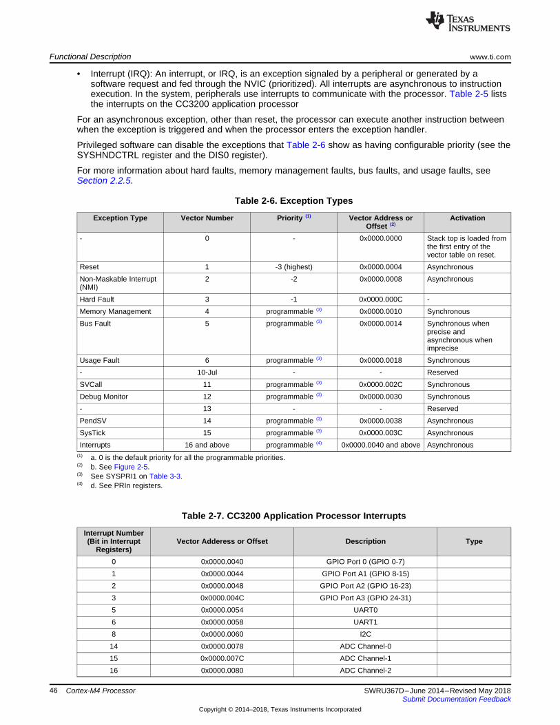
Functional Description www.ti.com
46 SWRU367D–June 2014–Revised May 2018Submit Documentation Feedback
Copyright © 2014–2018, Texas Instruments Incorporated
Cortex-M4 Processor
• Interrupt (IRQ): An interrupt, or IRQ, is an exception signaled by a peripheral or generated by asoftware request and fed through the NVIC (prioritized). All interrupts are asynchronous to instructionexecution. In the system, peripherals use interrupts to communicate with the processor. Table 2-5 liststhe interrupts on the CC3200 application processor
For an asynchronous exception, other than reset, the processor can execute another instruction betweenwhen the exception is triggered and when the processor enters the exception handler.
Privileged software can disable the exceptions that Table 2-6 show as having configurable priority (see theSYSHNDCTRL register and the DIS0 register).
For more information about hard faults, memory management faults, bus faults, and usage faults, seeSection 2.2.5.
(1) a. 0 is the default priority for all the programmable priorities.(2) b. See Figure 2-5.(3) See SYSPRI1 on Table 3-3.(4) d. See PRIn registers.
Table 2-6. Exception Types
Exception Type Vector Number Priority (1) Vector Address orOffset (2)
Activation
- 0 - 0x0000.0000 Stack top is loaded fromthe first entry of thevector table on reset.
Reset 1 -3 (highest) 0x0000.0004 AsynchronousNon-Maskable Interrupt(NMI)
2 -2 0x0000.0008 Asynchronous
Hard Fault 3 -1 0x0000.000C -Memory Management 4 programmable (3) 0x0000.0010 SynchronousBus Fault 5 programmable (3) 0x0000.0014 Synchronous when
precise andasynchronous whenimprecise
Usage Fault 6 programmable (3) 0x0000.0018 Synchronous- 10-Jul - - ReservedSVCall 11 programmable (3) 0x0000.002C SynchronousDebug Monitor 12 programmable (3) 0x0000.0030 Synchronous- 13 - - ReservedPendSV 14 programmable (3) 0x0000.0038 AsynchronousSysTick 15 programmable (3) 0x0000.003C AsynchronousInterrupts 16 and above programmable (4) 0x0000.0040 and above Asynchronous
Table 2-7. CC3200 Application Processor Interrupts
Interrupt Number(Bit in Interrupt
Registers)Vector Adderess or Offset Description Type
0 0x0000.0040 GPIO Port 0 (GPIO 0-7)1 0x0000.0044 GPIO Port A1 (GPIO 8-15)2 0x0000.0048 GPIO Port A2 (GPIO 16-23)3 0x0000.004C GPIO Port A3 (GPIO 24-31)5 0x0000.0054 UART06 0x0000.0058 UART18 0x0000.0060 I2C14 0x0000.0078 ADC Channel-015 0x0000.007C ADC Channel-116 0x0000.0080 ADC Channel-2
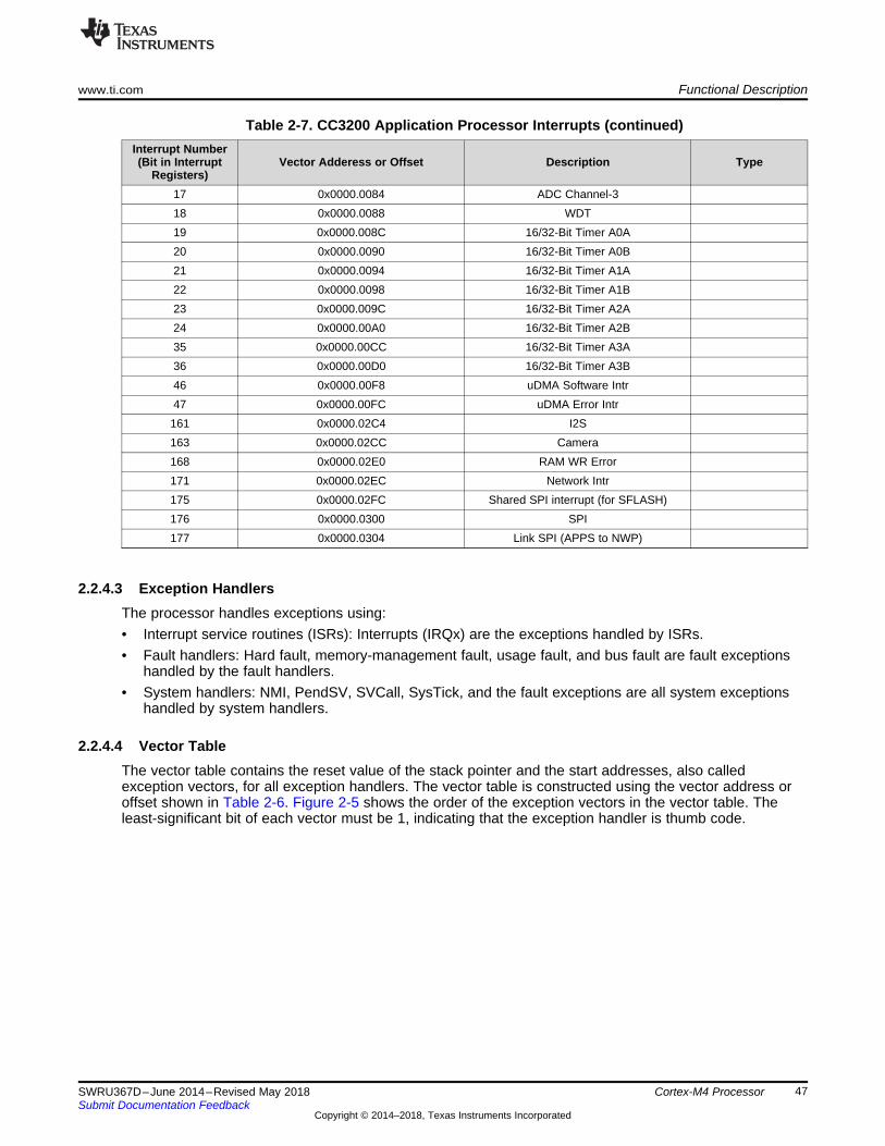
www.ti.com Functional Description
47SWRU367D–June 2014–Revised May 2018Submit Documentation Feedback
Copyright © 2014–2018, Texas Instruments Incorporated
Cortex-M4 Processor
Table 2-7. CC3200 Application Processor Interrupts (continued)Interrupt Number(Bit in Interrupt
Registers)Vector Adderess or Offset Description Type
17 0x0000.0084 ADC Channel-318 0x0000.0088 WDT19 0x0000.008C 16/32-Bit Timer A0A20 0x0000.0090 16/32-Bit Timer A0B21 0x0000.0094 16/32-Bit Timer A1A22 0x0000.0098 16/32-Bit Timer A1B23 0x0000.009C 16/32-Bit Timer A2A24 0x0000.00A0 16/32-Bit Timer A2B35 0x0000.00CC 16/32-Bit Timer A3A36 0x0000.00D0 16/32-Bit Timer A3B46 0x0000.00F8 uDMA Software Intr47 0x0000.00FC uDMA Error Intr161 0x0000.02C4 I2S163 0x0000.02CC Camera168 0x0000.02E0 RAM WR Error171 0x0000.02EC Network Intr175 0x0000.02FC Shared SPI interrupt (for SFLASH)176 0x0000.0300 SPI177 0x0000.0304 Link SPI (APPS to NWP)
2.2.4.3 Exception HandlersThe processor handles exceptions using:• Interrupt service routines (ISRs): Interrupts (IRQx) are the exceptions handled by ISRs.• Fault handlers: Hard fault, memory-management fault, usage fault, and bus fault are fault exceptions
handled by the fault handlers.• System handlers: NMI, PendSV, SVCall, SysTick, and the fault exceptions are all system exceptions
handled by system handlers.
2.2.4.4 Vector TableThe vector table contains the reset value of the stack pointer and the start addresses, also calledexception vectors, for all exception handlers. The vector table is constructed using the vector address oroffset shown in Table 2-6. Figure 2-5 shows the order of the exception vectors in the vector table. Theleast-significant bit of each vector must be 1, indicating that the exception handler is thumb code.
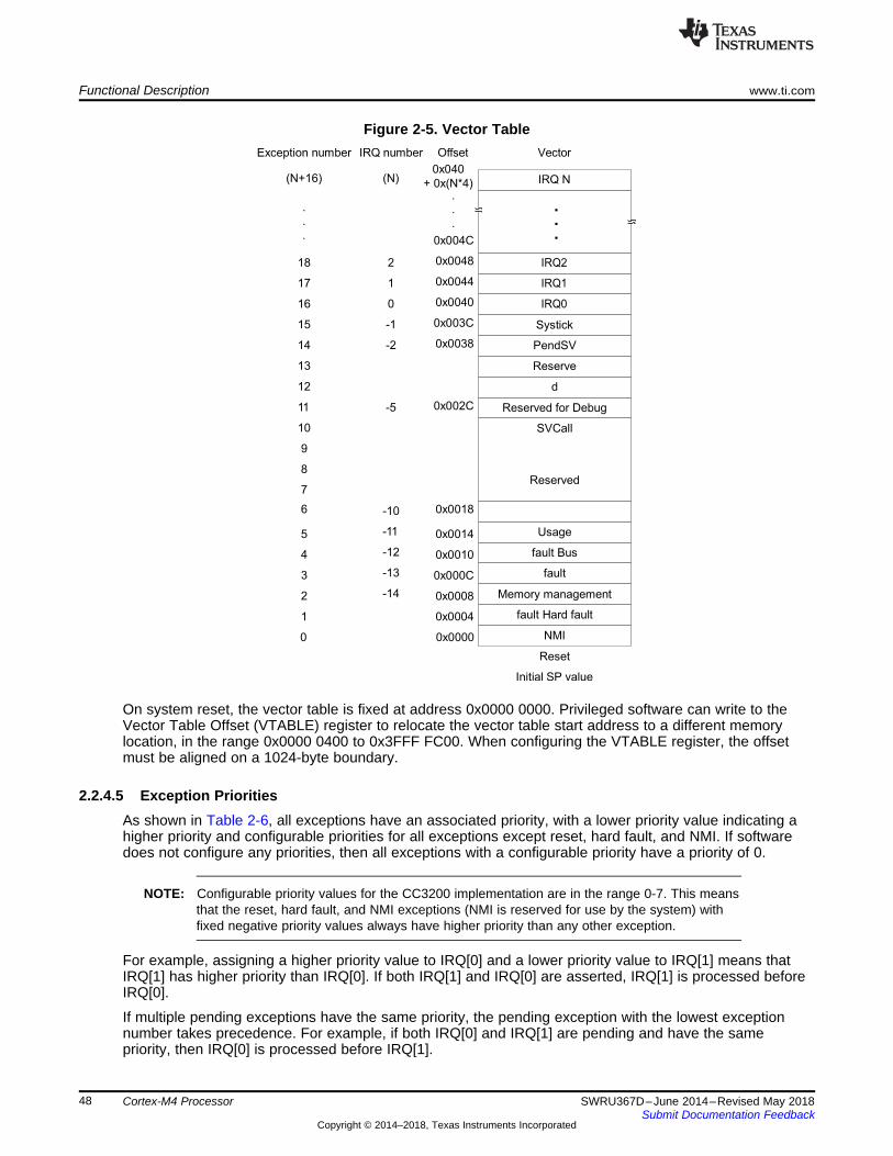
Exception number
(N+16)
.
.
.
18
17
16
15
14
13
12
11
10
9
8
7
6
5
4
3
2
1
0
IRQ number
(N)
2
1
0
-1
-2
-5
-10
-11
-12
-13
-14
Offset
0x040
+ 0x(N*4).
.
.
0x004C
0x0048
0x0044
0x0040
0x003C
0x0038
0x002C
0x0018
0x0014
0x0010
0x000C
0x0008
0x0004
0x0000
Vector
IRQ N
.
.
.
IRQ2
IRQ1
IRQ0
Systick
PendSV
Reserve
d
Reserved for Debug
SVCall
Reserved
Usage
fault Bus
fault
Memory management
fault Hard fault
NMI
Reset
Initial SP value
Functional Description www.ti.com
48 SWRU367D–June 2014–Revised May 2018Submit Documentation Feedback
Copyright © 2014–2018, Texas Instruments Incorporated
Cortex-M4 Processor
Figure 2-5. Vector Table
On system reset, the vector table is fixed at address 0x0000 0000. Privileged software can write to theVector Table Offset (VTABLE) register to relocate the vector table start address to a different memorylocation, in the range 0x0000 0400 to 0x3FFF FC00. When configuring the VTABLE register, the offsetmust be aligned on a 1024-byte boundary.
2.2.4.5 Exception PrioritiesAs shown in Table 2-6, all exceptions have an associated priority, with a lower priority value indicating ahigher priority and configurable priorities for all exceptions except reset, hard fault, and NMI. If softwaredoes not configure any priorities, then all exceptions with a configurable priority have a priority of 0.
NOTE: Configurable priority values for the CC3200 implementation are in the range 0-7. This meansthat the reset, hard fault, and NMI exceptions (NMI is reserved for use by the system) withfixed negative priority values always have higher priority than any other exception.
For example, assigning a higher priority value to IRQ[0] and a lower priority value to IRQ[1] means thatIRQ[1] has higher priority than IRQ[0]. If both IRQ[1] and IRQ[0] are asserted, IRQ[1] is processed beforeIRQ[0].
If multiple pending exceptions have the same priority, the pending exception with the lowest exceptionnumber takes precedence. For example, if both IRQ[0] and IRQ[1] are pending and have the samepriority, then IRQ[0] is processed before IRQ[1].
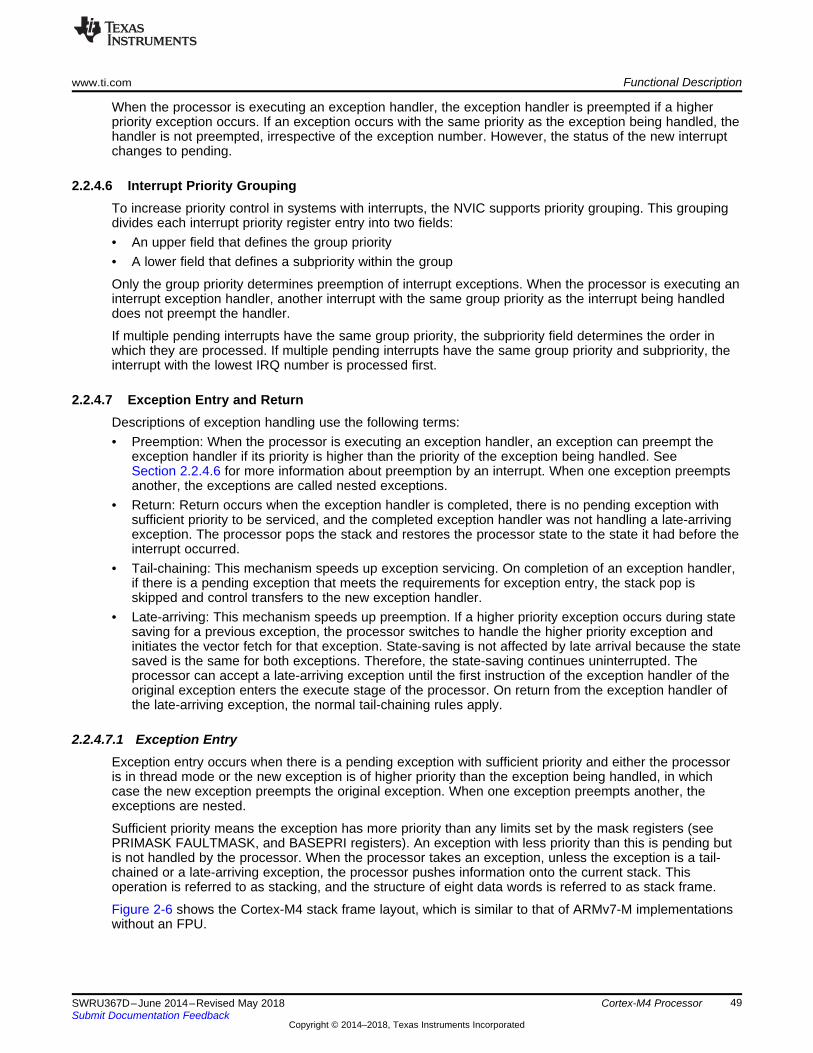
www.ti.com Functional Description
49SWRU367D–June 2014–Revised May 2018Submit Documentation Feedback
Copyright © 2014–2018, Texas Instruments Incorporated
Cortex-M4 Processor
When the processor is executing an exception handler, the exception handler is preempted if a higherpriority exception occurs. If an exception occurs with the same priority as the exception being handled, thehandler is not preempted, irrespective of the exception number. However, the status of the new interruptchanges to pending.
2.2.4.6 Interrupt Priority GroupingTo increase priority control in systems with interrupts, the NVIC supports priority grouping. This groupingdivides each interrupt priority register entry into two fields:• An upper field that defines the group priority• A lower field that defines a subpriority within the group
Only the group priority determines preemption of interrupt exceptions. When the processor is executing aninterrupt exception handler, another interrupt with the same group priority as the interrupt being handleddoes not preempt the handler.
If multiple pending interrupts have the same group priority, the subpriority field determines the order inwhich they are processed. If multiple pending interrupts have the same group priority and subpriority, theinterrupt with the lowest IRQ number is processed first.
2.2.4.7 Exception Entry and ReturnDescriptions of exception handling use the following terms:• Preemption: When the processor is executing an exception handler, an exception can preempt the
exception handler if its priority is higher than the priority of the exception being handled. SeeSection 2.2.4.6 for more information about preemption by an interrupt. When one exception preemptsanother, the exceptions are called nested exceptions.
• Return: Return occurs when the exception handler is completed, there is no pending exception withsufficient priority to be serviced, and the completed exception handler was not handling a late-arrivingexception. The processor pops the stack and restores the processor state to the state it had before theinterrupt occurred.
• Tail-chaining: This mechanism speeds up exception servicing. On completion of an exception handler,if there is a pending exception that meets the requirements for exception entry, the stack pop isskipped and control transfers to the new exception handler.
• Late-arriving: This mechanism speeds up preemption. If a higher priority exception occurs during statesaving for a previous exception, the processor switches to handle the higher priority exception andinitiates the vector fetch for that exception. State-saving is not affected by late arrival because the statesaved is the same for both exceptions. Therefore, the state-saving continues uninterrupted. Theprocessor can accept a late-arriving exception until the first instruction of the exception handler of theoriginal exception enters the execute stage of the processor. On return from the exception handler ofthe late-arriving exception, the normal tail-chaining rules apply.
2.2.4.7.1 Exception EntryException entry occurs when there is a pending exception with sufficient priority and either the processoris in thread mode or the new exception is of higher priority than the exception being handled, in whichcase the new exception preempts the original exception. When one exception preempts another, theexceptions are nested.
Sufficient priority means the exception has more priority than any limits set by the mask registers (seePRIMASK FAULTMASK, and BASEPRI registers). An exception with less priority than this is pending butis not handled by the processor. When the processor takes an exception, unless the exception is a tail-chained or a late-arriving exception, the processor pushes information onto the current stack. Thisoperation is referred to as stacking, and the structure of eight data words is referred to as stack frame.
Figure 2-6 shows the Cortex-M4 stack frame layout, which is similar to that of ARMv7-M implementationswithout an FPU.
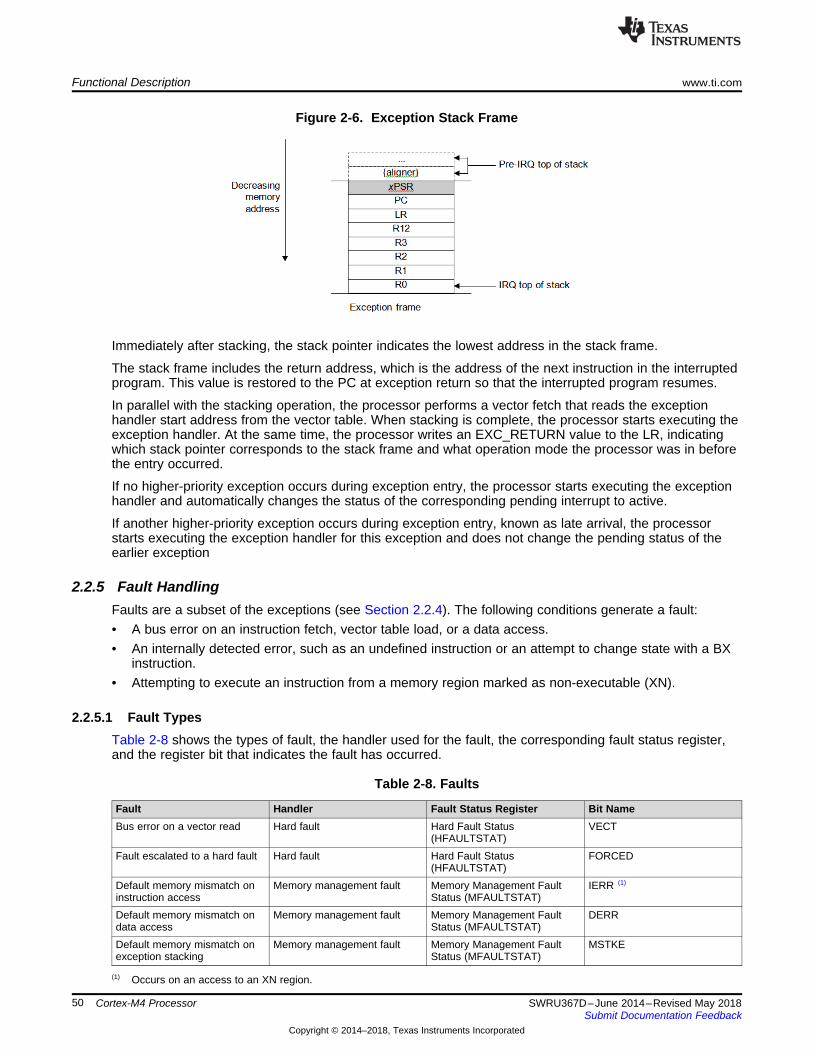
Functional Description www.ti.com
50 SWRU367D–June 2014–Revised May 2018Submit Documentation Feedback
Copyright © 2014–2018, Texas Instruments Incorporated
Cortex-M4 Processor
Figure 2-6. Exception Stack Frame
Immediately after stacking, the stack pointer indicates the lowest address in the stack frame.
The stack frame includes the return address, which is the address of the next instruction in the interruptedprogram. This value is restored to the PC at exception return so that the interrupted program resumes.
In parallel with the stacking operation, the processor performs a vector fetch that reads the exceptionhandler start address from the vector table. When stacking is complete, the processor starts executing theexception handler. At the same time, the processor writes an EXC_RETURN value to the LR, indicatingwhich stack pointer corresponds to the stack frame and what operation mode the processor was in beforethe entry occurred.
If no higher-priority exception occurs during exception entry, the processor starts executing the exceptionhandler and automatically changes the status of the corresponding pending interrupt to active.
If another higher-priority exception occurs during exception entry, known as late arrival, the processorstarts executing the exception handler for this exception and does not change the pending status of theearlier exception
2.2.5 Fault HandlingFaults are a subset of the exceptions (see Section 2.2.4). The following conditions generate a fault:• A bus error on an instruction fetch, vector table load, or a data access.• An internally detected error, such as an undefined instruction or an attempt to change state with a BX
instruction.• Attempting to execute an instruction from a memory region marked as non-executable (XN).
2.2.5.1 Fault TypesTable 2-8 shows the types of fault, the handler used for the fault, the corresponding fault status register,and the register bit that indicates the fault has occurred.
(1) Occurs on an access to an XN region.
Table 2-8. Faults
Fault Handler Fault Status Register Bit NameBus error on a vector read Hard fault Hard Fault Status
(HFAULTSTAT)VECT
Fault escalated to a hard fault Hard fault Hard Fault Status(HFAULTSTAT)
FORCED
Default memory mismatch oninstruction access
Memory management fault Memory Management FaultStatus (MFAULTSTAT)
IERR (1)
Default memory mismatch ondata access
Memory management fault Memory Management FaultStatus (MFAULTSTAT)
DERR
Default memory mismatch onexception stacking
Memory management fault Memory Management FaultStatus (MFAULTSTAT)
MSTKE
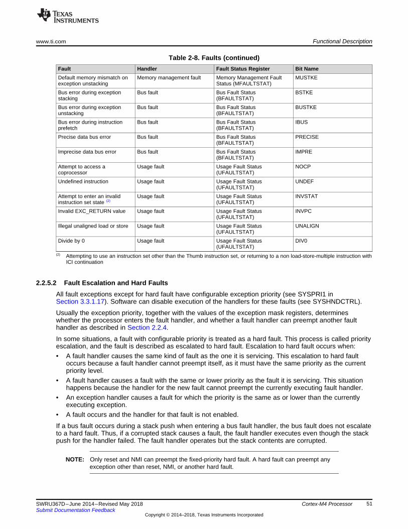
www.ti.com Functional Description
51SWRU367D–June 2014–Revised May 2018Submit Documentation Feedback
Copyright © 2014–2018, Texas Instruments Incorporated
Cortex-M4 Processor
Table 2-8. Faults (continued)Fault Handler Fault Status Register Bit Name
(2) Attempting to use an instruction set other than the Thumb instruction set, or returning to a non load-store-multiple instruction withICI continuation
Default memory mismatch onexception unstacking
Memory management fault Memory Management FaultStatus (MFAULTSTAT)
MUSTKE
Bus error during exceptionstacking
Bus fault Bus Fault Status(BFAULTSTAT)
BSTKE
Bus error during exceptionunstacking
Bus fault Bus Fault Status(BFAULTSTAT)
BUSTKE
Bus error during instructionprefetch
Bus fault Bus Fault Status(BFAULTSTAT)
IBUS
Precise data bus error Bus fault Bus Fault Status(BFAULTSTAT)
PRECISE
Imprecise data bus error Bus fault Bus Fault Status(BFAULTSTAT)
IMPRE
Attempt to access acoprocessor
Usage fault Usage Fault Status(UFAULTSTAT)
NOCP
Undefined instruction Usage fault Usage Fault Status(UFAULTSTAT)
UNDEF
Attempt to enter an invalidinstruction set state (2)
Usage fault Usage Fault Status(UFAULTSTAT)
INVSTAT
Invalid EXC_RETURN value Usage fault Usage Fault Status(UFAULTSTAT)
INVPC
Illegal unaligned load or store Usage fault Usage Fault Status(UFAULTSTAT)
UNALIGN
Divide by 0 Usage fault Usage Fault Status(UFAULTSTAT)
DIV0
2.2.5.2 Fault Escalation and Hard FaultsAll fault exceptions except for hard fault have configurable exception priority (see SYSPRI1 inSection 3.3.1.17). Software can disable execution of the handlers for these faults (see SYSHNDCTRL).
Usually the exception priority, together with the values of the exception mask registers, determineswhether the processor enters the fault handler, and whether a fault handler can preempt another faulthandler as described in Section 2.2.4.
In some situations, a fault with configurable priority is treated as a hard fault. This process is called priorityescalation, and the fault is described as escalated to hard fault. Escalation to hard fault occurs when:• A fault handler causes the same kind of fault as the one it is servicing. This escalation to hard fault
occurs because a fault handler cannot preempt itself, as it must have the same priority as the currentpriority level.
• A fault handler causes a fault with the same or lower priority as the fault it is servicing. This situationhappens because the handler for the new fault cannot preempt the currently executing fault handler.
• An exception handler causes a fault for which the priority is the same as or lower than the currentlyexecuting exception.
• A fault occurs and the handler for that fault is not enabled.
If a bus fault occurs during a stack push when entering a bus fault handler, the bus fault does not escalateto a hard fault. Thus, if a corrupted stack causes a fault, the fault handler executes even though the stackpush for the handler failed. The fault handler operates but the stack contents are corrupted.
NOTE: Only reset and NMI can preempt the fixed-priority hard fault. A hard fault can preempt anyexception other than reset, NMI, or another hard fault.
Functional Description www.ti.com
52 SWRU367D–June 2014–Revised May 2018Submit Documentation Feedback
Copyright © 2014–2018, Texas Instruments Incorporated
Cortex-M4 Processor
2.2.5.3 Fault Status Registers and Fault Address RegistersThe fault status registers indicate the cause of a fault. For bus faults and memory management faults, thefault address register indicates the address accessed by the operation that caused the fault, as shown inTable 2-9.
Table 2-9. Fault Status and Fault Address Registers
Handler Status Register Name Address Register Name Register DescriptionHard fault Hard Fault Status
(HFAULTSTAT)- Section 3.3.1.22
Memory management fault Memory Management FaultStatus (MFAULTSTAT)
Memory Management FaultAddress (MMADDR)
Section 3.3.1.23
Bus fault Bus Fault Status(BFAULTSTAT)
Bus Fault Address(FAULTADDR)
Section 3.3.1.23
Usage fault Usage Fault Status(UFAULTSTAT)
- Section 3.3.1.23
2.2.5.4 LockupThe processor enters a lockup state if a hard fault occurs when executing the NMI or hard fault handlers.When the processor is in the lockup state, it does not execute any instructions. The processor remains inlockup state until it is reset, an NMI occurs, or it is halted by a debugger.
2.2.6 Power ManagementThe CC3200 Wi-Fi microcontroller is a multi-processor system-on-chip. An advanced power managementscheme has been implemented at chip level that delivers the best-in-class energy efficiency across a wideclass of application profiles, while handling the asynchronous sleep-wake requirements of multiple highperformance processors and Wi-Fi radio subsystems. The Cortex-M4 application processor subsystem(consisting of the CM4 core and application peripherals) is a subset of this.
The chip-level power management scheme is such that the application program is unaware of the powerstate transitions of the other subsystems. This approach insulates the user from the complexities of amulti-processor system and simplifies the application development process.
From the Cortex-M4 application processor standpoint, CC3200 supports the typical SLEEP andDEEPSLEEP modes similar to those in discrete microcontrollers. The following section describe these twomodes.
In addition to SLEEP and DEEPSLEEP, two additional sleep modes are offered. These two modesconsume much lower power than the DEEPSLEEP mode in CC3200.• Low Power Deep Sleep Mode (LPDS)
– Recommended for ultra-low power always-connected cloud and Wi-Fi applications– Up to 256Kbyte of SRAM retention and fast wakeup (<5 mS)– When networking and Wi-Fi subsystems are disabled, the MCU draws less than 100 µA with
256Kbyte of SRAM retained (code and data). Total system current (incl Wi-Fi and network periodicwake-up) as low as 700 µA
– Processor and peripheral registers are not retained. Global always ON configurations at SoC levelare retained.
• Hibernate Mode (HIB)– Recommended for ultra-low power in-frequently connected cloud and Wi-Fi applications– Ultra low current of 4 µA, including RTC– Wake on RTC or selected GPIO– No SRAM or logic retention. 2 × 32 bit register retention.
LPDS and HIB modes will be covered in more detail in the Power Clock and Reset Management chapter.
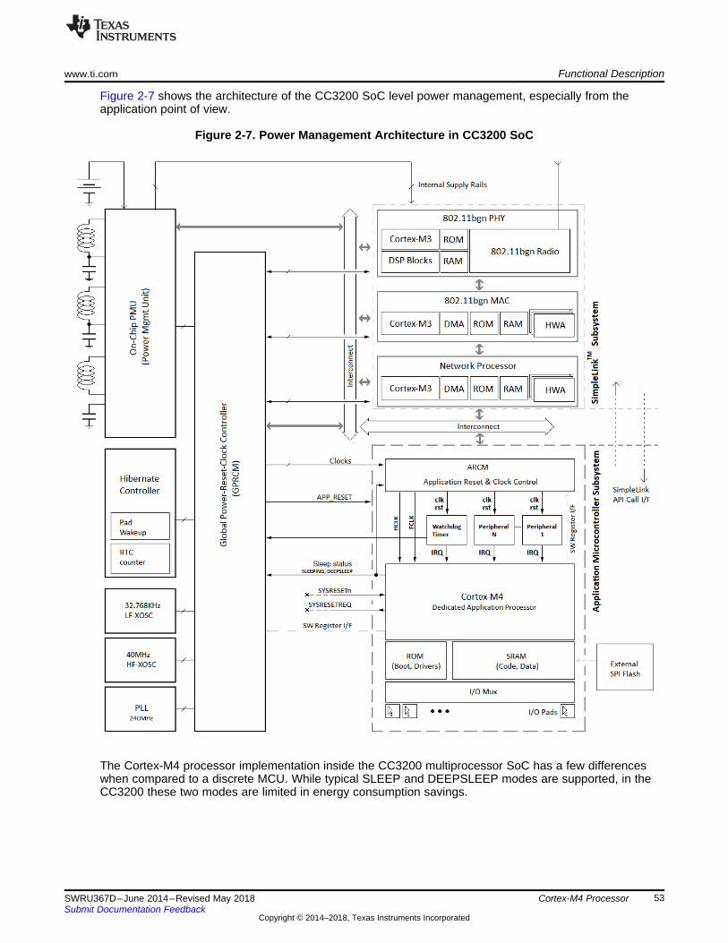
www.ti.com Functional Description
53SWRU367D–June 2014–Revised May 2018Submit Documentation Feedback
Copyright © 2014–2018, Texas Instruments Incorporated
Cortex-M4 Processor
Figure 2-7 shows the architecture of the CC3200 SoC level power management, especially from theapplication point of view.
Figure 2-7. Power Management Architecture in CC3200 SoC
The Cortex-M4 processor implementation inside the CC3200 multiprocessor SoC has a few differenceswhen compared to a discrete MCU. While typical SLEEP and DEEPSLEEP modes are supported, in theCC3200 these two modes are limited in energy consumption savings.
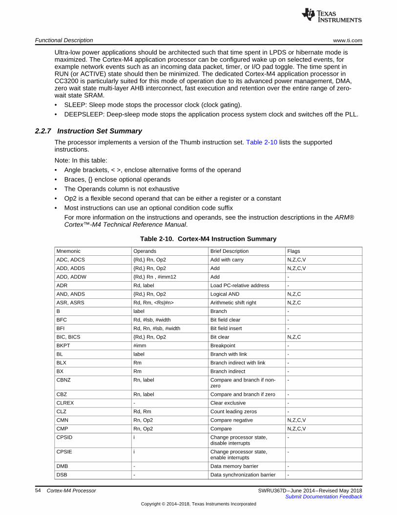
Functional Description www.ti.com
54 SWRU367D–June 2014–Revised May 2018Submit Documentation Feedback
Copyright © 2014–2018, Texas Instruments Incorporated
Cortex-M4 Processor
Ultra-low power applications should be architected such that time spent in LPDS or hibernate mode ismaximized. The Cortex-M4 application processor can be configured wake up on selected events, forexample network events such as an incoming data packet, timer, or I/O pad toggle. The time spent inRUN (or ACTIVE) state should then be minimized. The dedicated Cortex-M4 application processor inCC3200 is particularly suited for this mode of operation due to its advanced power management, DMA,zero wait state multi-layer AHB interconnect, fast execution and retention over the entire range of zero-wait state SRAM.• SLEEP: Sleep mode stops the processor clock (clock gating).• DEEPSLEEP: Deep-sleep mode stops the application process system clock and switches off the PLL.
2.2.7 Instruction Set SummaryThe processor implements a version of the Thumb instruction set. Table 2-10 lists the supportedinstructions.
Note: In this table:• Angle brackets, < >, enclose alternative forms of the operand• Braces, enclose optional operands• The Operands column is not exhaustive• Op2 is a flexible second operand that can be either a register or a constant• Most instructions can use an optional condition code suffix
For more information on the instructions and operands, see the instruction descriptions in the ARM®Cortex™-M4 Technical Reference Manual.
Table 2-10. Cortex-M4 Instruction Summary
Mnemonic Operands Brief Description FlagsADC, ADCS Rd, Rn, Op2 Add with carry N,Z,C,VADD, ADDS Rd, Rn, Op2 Add N,Z,C,VADD, ADDW Rd, Rn , #imm12 Add -ADR Rd, label Load PC-relative address -AND, ANDS Rd, Rn, Op2 Logical AND N,Z,CASR, ASRS Rd, Rm, <Rs|#n> Arithmetic shift right N,Z,CB label Branch -BFC Rd, #lsb, #width Bit field clear -BFI Rd, Rn, #lsb, #width Bit field insert -BIC, BICS Rd, Rn, Op2 Bit clear N,Z,CBKPT #imm Breakpoint -BL label Branch with link -BLX Rm Branch indirect with link -BX Rm Branch indirect -CBNZ Rn, label Compare and branch if non-
zero-
CBZ Rn, label Compare and branch if zero -CLREX - Clear exclusive -CLZ Rd, Rm Count leading zeros -CMN Rn, Op2 Compare negative N,Z,C,VCMP Rn, Op2 Compare N,Z,C,VCPSID i Change processor state,
disable interrupts-
CPSIE i Change processor state,enable interrupts
-
DMB - Data memory barrier -DSB - Data synchronization barrier -
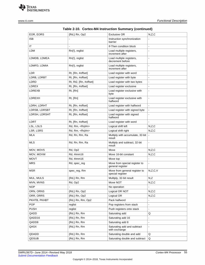
www.ti.com Functional Description
55SWRU367D–June 2014–Revised May 2018Submit Documentation Feedback
Copyright © 2014–2018, Texas Instruments Incorporated
Cortex-M4 Processor
Table 2-10. Cortex-M4 Instruction Summary (continued)EOR, EORS Rd, Rn, Op2 Exclusive OR N,Z,CISB - Instruction synchronization
barrier-
IT - If-Then condition block -LDM Rn!, reglist Load multiple registers,
increment after-
LDMDB, LDMEA Rn!, reglist Load multiple registers,decrement before
-
LDMFD, LDMIA Rn!, reglist Load multiple registers,increment after
-
LDR Rt, [Rn, #offset] Load register with word -LDRB, LDRBT Rt, [Rn, #offset] Load register with byte -LDRD Rt, Rt2, [Rn, #offset] Load register with two bytes -LDREX Rt, [Rn, #offset] Load register exclusive -LDREXB Rt, [Rn] Load register exclusive with
byte-
LDREXH Rt, [Rn] Load register exclusive withhalfword
-
LDRH, LDRHT Rt, [Rn, #offset] Load register with halfword -LDRSB, LDRSBT Rt, [Rn, #offset] Load register with signed byte -LDRSH, LDRSHT Rt, [Rn, #offset] Load register with signed
halfword-
LDRT Rt, [Rn, #offset] Load register with word -LSL, LSLS Rd, Rm, <Rs|#n> Logical shift left N,Z,CLSR, LSRS Rd, Rm, <Rs|#n> Logical shift right N,Z,CMLA Rd, Rn, Rm, Ra Multiply with accumulate, 32-bit
result-
MLS Rd, Rn, Rm, Ra Multiply and subtract, 32-bitresult
-
MOV, MOVS Rd, Op2 Move N,Z,CMOV, MOVW Rd, #imm16 Move 16-bit constant N,Z,CMOVT Rd, #imm16 Move top -MRS Rd, spec_reg Move from special register to
general register-
MSR spec_reg, Rm Move from general register tospecial register
N,Z,C,V
MUL, MULS Rd, Rn, Rm Multiply, 32-bit result N,ZMVN, MVNS Rd, Op2 Move NOT N,Z,CNOP - No operation -ORN, ORNS Rd, Rn, Op2 Logical OR NOT N,Z,CORR, ORRS Rd, Rn, Op2 Logical OR N,Z,CPKHTB, PKHBT Rd, Rn, Rm, Op2 Pack halfword -POP reglist Pop registers from stack -PUSH reglist Push registers onto stack -QADD Rd, Rn, Rm Saturating add QQADD16 Rd, Rn, Rm Saturating add 16 -QADD8 Rd, Rn, Rm Saturating add 8 -QASX Rd, Rn, Rm Saturating add and subtract
with exchange-
QDADD Rd, Rn, Rm Saturating double and add QQDSUB Rd, Rn, Rm Saturating double and subtract Q
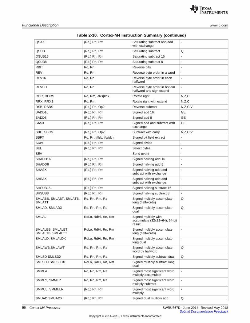
Functional Description www.ti.com
56 SWRU367D–June 2014–Revised May 2018Submit Documentation Feedback
Copyright © 2014–2018, Texas Instruments Incorporated
Cortex-M4 Processor
Table 2-10. Cortex-M4 Instruction Summary (continued)QSAX Rd, Rn, Rm Saturating subtract and add
with exchange-
QSUB Rd, Rn, Rm Saturating subtract QQSUB16 Rd, Rn, Rm Saturating subtract 16 -QSUB8 Rd, Rn, Rm Saturating subtract 8 -RBIT Rd, Rn Reverse bits -REV Rd, Rn Reverse byte order in a word -REV16 Rd, Rn Reverse byte order in each
halfword-
REVSH Rd, Rn Reverse byte order in bottomhalfword and sign extend
-
ROR, RORS Rd, Rm, <Rs|#n> Rotate right N,Z,CRRX, RRXS Rd, Rm Rotate right with extend N,Z,CRSB, RSBS Rd, Rn, Op2 Reverse subtract N,Z,C,VSADD16 Rd, Rn, Rm Signed add 16 GESADD8 Rd, Rn, Rm Signed add 8 GESASX Rd, Rn, Rm Signed add and subtract with
exchangeGE
SBC, SBCS Rd, Rn, Op2 Subtract with carry N,Z,C,VSBFX Rd, Rn, #lsb, #width Signed bit field extract -SDIV Rd, Rn, Rm Signed divide -SEL Rd, Rn, Rm Select bytes -SEV - Send event -SHADD16 Rd, Rn, Rm Signed halving add 16 -SHADD8 Rd, Rn, Rm Signed halving add 8 -SHASX Rd, Rn, Rm Signed halving add and
subtract with exchange-
SHSAX Rd, Rn, Rm Signed halving add andsubtract with exchange
-
SHSUB16 Rd, Rn, Rm Signed halving subtract 16 -SHSUB8 Rd, Rn, Rm Signed halving subtract 8 -SMLABB, SMLABT, SMLATB,SMLATT
Rd, Rn, Rm, Ra Signed multiply accumulatelong (halfwords)
Q
SMLAD, SMLADX Rd, Rn, Rm, Ra Signed multiply accumulatedual
Q
SMLAL RdLo, RdHi, Rn, Rm Signed multiply withaccumulate (32x32+64), 64-bitresult
-
SMLALBB, SMLALBT,SMLALTB, SMLALTT
RdLo, RdHi, Rn, Rm Signed multiply accumulatelong (halfwords)
-
SMLALD, SMLALDX RdLo, RdHi, Rn, Rm Signed multiply accumulatelong dual
-
SMLAWB,SMLAWT Rd, Rn, Rm, Ra Signed multiply accumulate,word by halfword
Q
SMLSD SMLSDX Rd, Rn, Rm, Ra Signed multiply subtract dual QSMLSLD SMLSLDX RdLo, RdHi, Rn, Rm Signed multiply subtract long
dualSMMLA Rd, Rn, Rm, Ra Signed most significant word
multiply accumulate-
SMMLS, SMMLR Rd, Rn, Rm, Ra Signed most significant wordmultiply subtract
-
SMMUL, SMMULR Rd, Rn, Rm Signed most significant wordmultiply
-
SMUAD SMUADX Rd, Rn, Rm Signed dual multiply add Q
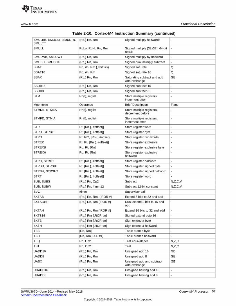
www.ti.com Functional Description
57SWRU367D–June 2014–Revised May 2018Submit Documentation Feedback
Copyright © 2014–2018, Texas Instruments Incorporated
Cortex-M4 Processor
Table 2-10. Cortex-M4 Instruction Summary (continued)SMULBB, SMULBT, SMULTB,SMULTT
Rd, Rn, Rm Signed multiply halfwords -
SMULL RdLo, RdHi, Rn, Rm Signed multiply (32x32), 64-bitresult
-
SMULWB, SMULWT Rd, Rn, Rm Signed multiply by halfword -SMUSD, SMUSDX Rd, Rn, Rm Signed dual multiply subtract -SSAT Rd, #n, Rm ,shift #s Signed saturate QSSAT16 Rd, #n, Rm Signed saturate 16 QSSAX Rd, Rn, Rm Saturating subtract and add
with exchangeGE
SSUB16 Rd, Rn, Rm Signed subtract 16 -SSUB8 Rd, Rn, Rm Signed subtract 8 -STM Rn!, reglist Store multiple registers,
increment after-
Mnemonic Operands Brief Description FlagsSTMDB, STMEA Rn!, reglist Store multiple registers,
decrement before-
STMFD, STMIA Rn!, reglist Store multiple registers,increment after
-
STR Rt, [Rn , #offset] Store register word -STRB, STRBT Rt, [Rn , #offset] Store register byte -STRD Rt, Rt2, [Rn , #offset] Store register two words -STREX Rt, Rt, [Rn , #offset] Store register exclusive -STREXB Rd, Rt, [Rn] Store register exclusive byte -STREXH Rd, Rt, [Rn] Store register exclusive
halfword-
STRH, STRHT Rt, [Rn , #offset] Store register halfword -STRSB, STRSBT Rt, [Rn , #offset] Store register signed byte -STRSH, STRSHT Rt, [Rn , #offset] Store register signed halfword -STRT Rt, [Rn , #offset] Store register word -SUB, SUBS Rd, Rn, Op2 Subtract N,Z,C,VSUB, SUBW Rd, Rn, #imm12 Subtract 12-bit constant N,Z,C,VSVC #imm Supervisor call -SXTAB Rd, Rn, Rm, ,ROR # Extend 8 bits to 32 and add -SXTAB16 Rd, Rn, Rm,,ROR # Dual extend 8 bits to 16 and
add-
SXTAH Rd, Rn, Rm,,ROR # Extend 16 bits to 32 and add -SXTB16 Rd, Rm ,ROR #n Signed extend byte 16 -SXTB Rd, Rm ,ROR #n Sign extend a byte -SXTH Rd, Rm ,ROR #n Sign extend a halfword -TBB [Rn, Rm] Table branch byte -TBH [Rn, Rm, LSL #1] Table branch halfword -TEQ Rn, Op2 Test equivalence N,Z,CTST Rn, Op2 Test N,Z,CUADD16 Rd, Rn, Rm Unsigned add 16 GEUADD8 Rd, Rn, Rm Unsigned add 8 GEUASX Rd, Rn, Rm Unsigned add and subtract
with exchangeGE
UHADD16 Rd, Rn, Rm Unsigned halving add 16 -UHADD8 Rd, Rn, Rm Unsigned halving add 8 -
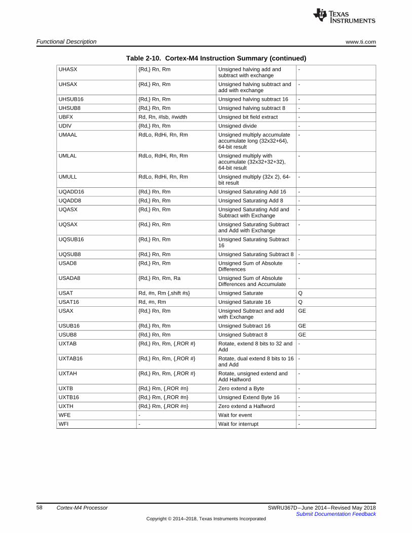
Functional Description www.ti.com
58 SWRU367D–June 2014–Revised May 2018Submit Documentation Feedback
Copyright © 2014–2018, Texas Instruments Incorporated
Cortex-M4 Processor
Table 2-10. Cortex-M4 Instruction Summary (continued)UHASX Rd, Rn, Rm Unsigned halving add and
subtract with exchange-
UHSAX Rd, Rn, Rm Unsigned halving subtract andadd with exchange
-
UHSUB16 Rd, Rn, Rm Unsigned halving subtract 16 -UHSUB8 Rd, Rn, Rm Unsigned halving subtract 8 -UBFX Rd, Rn, #lsb, #width Unsigned bit field extract -UDIV Rd, Rn, Rm Unsigned divide -UMAAL RdLo, RdHi, Rn, Rm Unsigned multiply accumulate
accumulate long (32x32+64),64-bit result
-
UMLAL RdLo, RdHi, Rn, Rm Unsigned multiply withaccumulate (32x32+32+32),64-bit result
-
UMULL RdLo, RdHi, Rn, Rm Unsigned multiply (32x 2), 64-bit result
-
UQADD16 Rd, Rn, Rm Unsigned Saturating Add 16 -UQADD8 Rd, Rn, Rm Unsigned Saturating Add 8 -UQASX Rd, Rn, Rm Unsigned Saturating Add and
Subtract with Exchange-
UQSAX Rd, Rn, Rm Unsigned Saturating Subtractand Add with Exchange
-
UQSUB16 Rd, Rn, Rm Unsigned Saturating Subtract16
-
UQSUB8 Rd, Rn, Rm Unsigned Saturating Subtract 8 -USAD8 Rd, Rn, Rm Unsigned Sum of Absolute
Differences-
USADA8 Rd, Rn, Rm, Ra Unsigned Sum of AbsoluteDifferences and Accumulate
-
USAT Rd, #n, Rm ,shift #s Unsigned Saturate QUSAT16 Rd, #n, Rm Unsigned Saturate 16 QUSAX Rd, Rn, Rm Unsigned Subtract and add
with ExchangeGE
USUB16 Rd, Rn, Rm Unsigned Subtract 16 GEUSUB8 Rd, Rn, Rm Unsigned Subtract 8 GEUXTAB Rd, Rn, Rm, ,ROR # Rotate, extend 8 bits to 32 and
Add-
UXTAB16 Rd, Rn, Rm, ,ROR # Rotate, dual extend 8 bits to 16and Add
-
UXTAH Rd, Rn, Rm, ,ROR # Rotate, unsigned extend andAdd Halfword
-
UXTB Rd, Rm, ,ROR #n Zero extend a Byte -UXTB16 Rd, Rm, ,ROR #n Unsigned Extend Byte 16 -UXTH Rd, Rm, ,ROR #n Zero extend a Halfword -WFE - Wait for event -WFI - Wait for interrupt -
59SWRU367D–June 2014–Revised May 2018Submit Documentation Feedback
Copyright © 2014–2018, Texas Instruments Incorporated
Cortex-M4 Peripherals
Chapter 3SWRU367D–June 2014–Revised May 2018
Cortex-M4 Peripherals
Topic ........................................................................................................................... Page
3.1 Overview ........................................................................................................... 603.2 Functional Description........................................................................................ 603.3 Register Map ..................................................................................................... 62
Overview www.ti.com
60 SWRU367D–June 2014–Revised May 2018Submit Documentation Feedback
Copyright © 2014–2018, Texas Instruments Incorporated
Cortex-M4 Peripherals
3.1 OverviewThis chapter provides information on the CC3200 implementation of the Cortex-M4 application processorin CC3200 peripherals, including:• SysTick (see Section 3.2.1) – Provides a simple, 24-bit clear-on-write, decrementing, wrap-on-zero
counter with a flexible control mechanism.• Nested Vectored Interrupt Controller (NVIC) (see Section 3.2.2) – Facilitates low-latency exception and
interrupt handling, controls power management, and implements system control registers.• System Control Block (SCB) (see Section 3.2.3) – Provides system implementation information and
system control, including configuration, control, and reporting of system exceptions.
Table 3-1 shows the address map of the private peripheral bus (PPB). Some peripheral register regionsare split into two address regions, as indicated by two addresses listed.
Table 3-1. Core Peripheral Register Regions
Address Core Peripheral0xE000.E010-0xE000.E01F System timer0xE000.E100-0xE000.E4EF Nested vectored interrupt controller0xE000.EF00-0xE000.EF030xE000.E008-0xE000.E00F0xE000.ED00-0xE000.ED3F
System control block
3.2 Functional DescriptionThis chapter provides information on the CC3200 implementation of the Cortex-M4 application processorin CC3200 peripherals: SysTick, NVIC, and SCB.
3.2.1 System Timer (SysTick)SysTick is an integrated system timer which provides a simple, 24-bit clear-on-write, decrementing, wrap-on-zero counter with a flexible control mechanism. The counter can be used in several different ways:• An RTOS tick timer that fires at a programmable rate (for example, 100 Hz) and invokes a SysTick
routine.• A high-speed alarm timer using the system clock.• A variable rate alarm or signal timer – The duration is range-dependent on the reference clock used
and the dynamic range of the counter.• A simple counter measuring time to completion and time used.• An internal clock source control based on missing or meeting durations. The COUNT bit in the
STCTRL control and status register can be used to determine if an action completed within a setduration, as part of a dynamic clock management control loop.
When enabled, the timer counts down on each clock from the reload value to zero, reloads (wraps) to thevalue in the STRELOAD register on the next clock edge, then decrements on subsequent clocks. Clearingthe STRELOAD register disables the counter on the next wrap. When the counter reaches zero, theCOUNT status bit is set. The COUNT bit clears on reads.
Writing to the STCURRENT register clears the register and the COUNT status bit. The write does nottrigger the SysTick exception logic. On a read, the current value is the value of the register at the time theregister is accessed.
The SysTick counter runs on the system clock. If this clock signal is stopped for low power mode, theSysTick counter stops. Ensure software uses aligned word accesses to access the SysTick registers.
The SysTick counter reload and current value are undefined at reset; the correct initialization sequence forthe SysTick counter is:1. Program the value in the STRELOAD register.2. Clear the STCURRENT register by writing to it with any value.
www.ti.com Functional Description
61SWRU367D–June 2014–Revised May 2018Submit Documentation Feedback
Copyright © 2014–2018, Texas Instruments Incorporated
Cortex-M4 Peripherals
3. Configure the STCTRL register for the required operation.
NOTE: When the processor is halted for debugging, the counter does not decrement.
3.2.2 Nested Vectored Interrupt Controller (NVIC)This section describes the nested vectored interrupt controller (NVIC) and the registers it uses. The NVICsupports:• A programmable priority level of 0-7 for each interrupt. A higher level corresponds to a lower priority,
so level 0 is the highest interrupt priority.• Low-latency exception and interrupt handling• Level and pulse detection of interrupt signals• Dynamic reprioritization of interrupts• Grouping of priority values into group priority and subpriority fields• Interrupt tail-chaining• An external non-maskable interrupt (NMI)
The processor automatically stacks its state on exception entry and unstacks this state on exception exit,with no instruction overhead, providing low latency exception handling.
3.2.2.1 Level-Sensitive and Pulse InterruptsThe processor supports both level-sensitive and pulse interrupts. Pulse interrupts are also described asedge-triggered interrupts.
A level-sensitive interrupt is held asserted until the peripheral deasserts the interrupt signal. Typically thishappens because the ISR accesses the peripheral, causing it to clear the interrupt request. A pulseinterrupt is an interrupt signal sampled synchronously on the rising edge of the processor clock. To ensurethe NVIC detects the interrupt, the peripheral must assert the interrupt signal for at least one clock cycle,during which the NVIC detects the pulse and latches the interrupt.
When the processor enters the ISR, it automatically removes the pending state from the interrupt (seeSection 3.2.2.2 for more information). For a level-sensitive interrupt, if the signal is not deasserted beforethe processor returns from the ISR, the interrupt becomes pending again, and the processor must executeits ISR again. As a result, the peripheral can hold the interrupt signal asserted until it no longer needsservicing.
3.2.2.2 Hardware and Software Control of InterruptsThe Cortex-M4 latches all interrupts. A peripheral interrupt becomes pending for one of the followingreasons:• The NVIC detects that the interrupt signal is High and the interrupt is not active.• The NVIC detects a rising edge on the interrupt signal.• Software writes to the corresponding interrupt set-pending register bit, or to the Software Trigger
Interrupt (SWTRIG) register to make a software-generated interrupt pending. See the INT bit in thePEND0 register or SWTRIG register.
A pending interrupt remains pending until one of the following:• The processor enters the ISR for the interrupt, changing the state of the interrupt from pending to
active. Then:– For a level-sensitive interrupt, when the processor returns from the ISR, the NVIC samples the
interrupt signal. If the signal is asserted, the state of the interrupt changes to pending, which mightcause the processor to immediately re-enter the ISR. Otherwise, the state of the interrupt changesto inactive.
– For a pulse interrupt, the NVIC continues to monitor the interrupt signal, and if this is pulsed, thestate of the interrupt changes to pending and active. In this case, when the processor returns fromthe ISR the state of the interrupt changes to pending, which might cause the processor to
Functional Description www.ti.com
62 SWRU367D–June 2014–Revised May 2018Submit Documentation Feedback
Copyright © 2014–2018, Texas Instruments Incorporated
Cortex-M4 Peripherals
immediately re-enter the ISR.If the interrupt signal is not pulsed while the processor is in the ISR, when the processor returnsfrom the ISR the state of the interrupt changes to inactive.
• Software writes to the corresponding interrupt clear-pending register bit– For a level-sensitive interrupt, if the interrupt signal is still asserted, the state of the interrupt does
not change. Otherwise, the state of the interrupt changes to inactive.– For a pulse interrupt, the state of the interrupt changes to inactive, if the state was pending or to
active, if the state was active and pending.
3.2.3 System Control Block (SCB)The system control block (SCB) provides system implementation information and system control, includingconfiguration, control, and reporting of the system exceptions.
3.3 Register MapTable 3-2 lists the Cortex-M4 Peripheral SysTick, NVIC, and SCB registers. The offset listed is ahexadecimal increment to the address of the register, relative to the core peripherals base address of0xE000 E000.
NOTE: Register spaces that are not used are reserved for future or internal use. Software shouldnot modify any reserved memory address.
Table 3-2. Peripherals Register Map
Offset Name Type Reset DescriptionSystem Timer (SysTick) Registers0x010 STCTRL R/W 0x0000.0000 SysTick Control and
Status Register0x014 STRELOAD R/W - SysTick Reload Value
Register0x018 STCURRENT R/WC - SysTick Current Value
RegisterNested Vectored Interrupt Controller (NVIC) Registers0x100 EN0 R/W 0x0000.0000 Interrupt 0-31 Set
Enable0x104 EN1 R/W 0x0000.0000 Interrupt 32-63 Set
Enable0x108 EN2 R/W 0x0000.0000 Interrupt 64-95 Set
Enable0x10C EN3 R/W 0x0000.0000 Interrupt 96-127 Set
Enable0x110 EN4 R/W 0x0000.0000 Interrupt 128-159 Set
Enable0x114 EN5 R/W 0x0000.0000 Interrupt 160- 191 Set
Enable0x118 EN6 R/W 0x0000.0000 Interrupt 192- 199 Set
Enable0x180 DIS0 R/W 0x0000.0000 Interrupt 0-31 Clear
Enable0x184 DIS1 R/W 0x0000.0000 Interrupt 32-63 Clear
Enable0x188 DIS2 R/W 0x0000.0000 Interrupt 64-95 Clear
Enable0x18C DIS3 R/W 0x0000.0000 Interrupt 96-127 Clear
Enable
www.ti.com Register Map
63SWRU367D–June 2014–Revised May 2018Submit Documentation Feedback
Copyright © 2014–2018, Texas Instruments Incorporated
Cortex-M4 Peripherals
Table 3-2. Peripherals Register Map (continued)Offset Name Type Reset Description0x190 DIS4 R/W 0x0000.0000 Interrupt 128-159 Clear
Enable0x194 DIS5 R/W 0x0000.0000 Interrupt 160-191 Clear
Enable0x198 DIS6 R/W 0x0000.0000 Interrupt 192 - 199 Clear
Enable0x200 PEND0 R/W 0x0000.0000 Interrupt 0-31 Set
Pending0x204 PEND1 R/W 0x0000.0000 Interrupt 32-63 Set
Pending0x208 PEND2 R/W 0x0000.0000 Interrupt 64-95 Set
Pending0x20C PEND3 R/W 0x0000.0000 Interrupt 96-127 Set
Pending0x210 PEND4 R/W 0x0000.0000 Interrupt 128-159 Set
Pending0x214 PEND5 R/W 0x0000.0000 Interrupt 160-191 Set
Pending0x218 PEND6 R/W 0x0000.0000 Interrupt 192-199 Set
Pending0x280 UNPEND0 R/W 0x0000.0000 Interrupt 0-31 Clear
Pending0x284 UNPEND1 R/W 0x0000.0000 Interrupt 32-63 Clear
Pending0x288 UNPEND2 R/W 0x0000.0000 Interrupt 64-95 Clear
Pending0x28C UNPEND3 R/W 0x0000.0000 Interrupt 96-127 Clear
Pending0x290 UNPEND4 R/W 0x0000.0000 Interrupt 128-159 Clear
Pending0x294 UNPEND5 R/W 0x0000.0000 Interrupt 160-191 Clear
Pending0x298 UNPEND6 R/W 0x0000.0000 Interrupt 192- 199 Clear
Pending0x300 ACTIVE0 RO 0x0000.0000 Interrupt 0-31 Active Bit0x304 ACTIVE1 RO 0x0000.0000 Interrupt 32-63 Active Bit0x308 ACTIVE2 RO 0x0000.0000 Interrupt 64-95 Active Bit0x30C ACTIVE3 RO 0x0000.0000 Interrupt 96-127 Active
Bit0x310 ACTIVE4 RO 0x0000.0000 Interrupt 128-159 Active
Bit0x314 ACTIVE5 RO 0x0000.0000 Interrupt 160-191 Active
Bit0x318 ACTIVE6 RO 0x0000.0000 Interrupt 192-199 Active
Bit0x400 PRI0 R/W 0x0000.0000 Interrupt 0-3 Priority0x404 PRI1 R/W 0x0000.0000 Interrupt 4-7 Priority0x408 PRI2 R/W 0x0000.0000 Interrupt 8-11 Priority0x40C PRI3 R/W 0x0000.0000 Interrupt 12-15 Priority0x410 PRI4 R/W 0x0000.0000 Interrupt 16-19 Priority0x414 PRI5 R/W 0x0000.0000 Interrupt 20-23 Priority0x418 PRI6 R/W 0x0000.0000 Interrupt 24-27 Priority0x41C PRI7 R/W 0x0000.0000 Interrupt 28-31 Priority0x420 PRI8 R/W 0x0000.0000 Interrupt 32-35 Priority
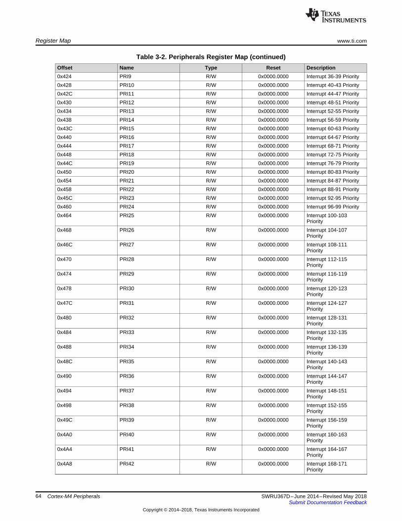
Register Map www.ti.com
64 SWRU367D–June 2014–Revised May 2018Submit Documentation Feedback
Copyright © 2014–2018, Texas Instruments Incorporated
Cortex-M4 Peripherals
Table 3-2. Peripherals Register Map (continued)Offset Name Type Reset Description0x424 PRI9 R/W 0x0000.0000 Interrupt 36-39 Priority0x428 PRI10 R/W 0x0000.0000 Interrupt 40-43 Priority0x42C PRI11 R/W 0x0000.0000 Interrupt 44-47 Priority0x430 PRI12 R/W 0x0000.0000 Interrupt 48-51 Priority0x434 PRI13 R/W 0x0000.0000 Interrupt 52-55 Priority0x438 PRI14 R/W 0x0000.0000 Interrupt 56-59 Priority0x43C PRI15 R/W 0x0000.0000 Interrupt 60-63 Priority0x440 PRI16 R/W 0x0000.0000 Interrupt 64-67 Priority0x444 PRI17 R/W 0x0000.0000 Interrupt 68-71 Priority0x448 PRI18 R/W 0x0000.0000 Interrupt 72-75 Priority0x44C PRI19 R/W 0x0000.0000 Interrupt 76-79 Priority0x450 PRI20 R/W 0x0000.0000 Interrupt 80-83 Priority0x454 PRI21 R/W 0x0000.0000 Interrupt 84-87 Priority0x458 PRI22 R/W 0x0000.0000 Interrupt 88-91 Priority0x45C PRI23 R/W 0x0000.0000 Interrupt 92-95 Priority0x460 PRI24 R/W 0x0000.0000 Interrupt 96-99 Priority0x464 PRI25 R/W 0x0000.0000 Interrupt 100-103
Priority0x468 PRI26 R/W 0x0000.0000 Interrupt 104-107
Priority0x46C PRI27 R/W 0x0000.0000 Interrupt 108-111
Priority0x470 PRI28 R/W 0x0000.0000 Interrupt 112-115
Priority0x474 PRI29 R/W 0x0000.0000 Interrupt 116-119
Priority0x478 PRI30 R/W 0x0000.0000 Interrupt 120-123
Priority0x47C PRI31 R/W 0x0000.0000 Interrupt 124-127
Priority0x480 PRI32 R/W 0x0000.0000 Interrupt 128-131
Priority0x484 PRI33 R/W 0x0000.0000 Interrupt 132-135
Priority0x488 PRI34 R/W 0x0000.0000 Interrupt 136-139
Priority0x48C PRI35 R/W 0x0000.0000 Interrupt 140-143
Priority0x490 PRI36 R/W 0x0000.0000 Interrupt 144-147
Priority0x494 PRI37 R/W 0x0000.0000 Interrupt 148-151
Priority0x498 PRI38 R/W 0x0000.0000 Interrupt 152-155
Priority0x49C PRI39 R/W 0x0000.0000 Interrupt 156-159
Priority0x4A0 PRI40 R/W 0x0000.0000 Interrupt 160-163
Priority0x4A4 PRI41 R/W 0x0000.0000 Interrupt 164-167
Priority0x4A8 PRI42 R/W 0x0000.0000 Interrupt 168-171
Priority
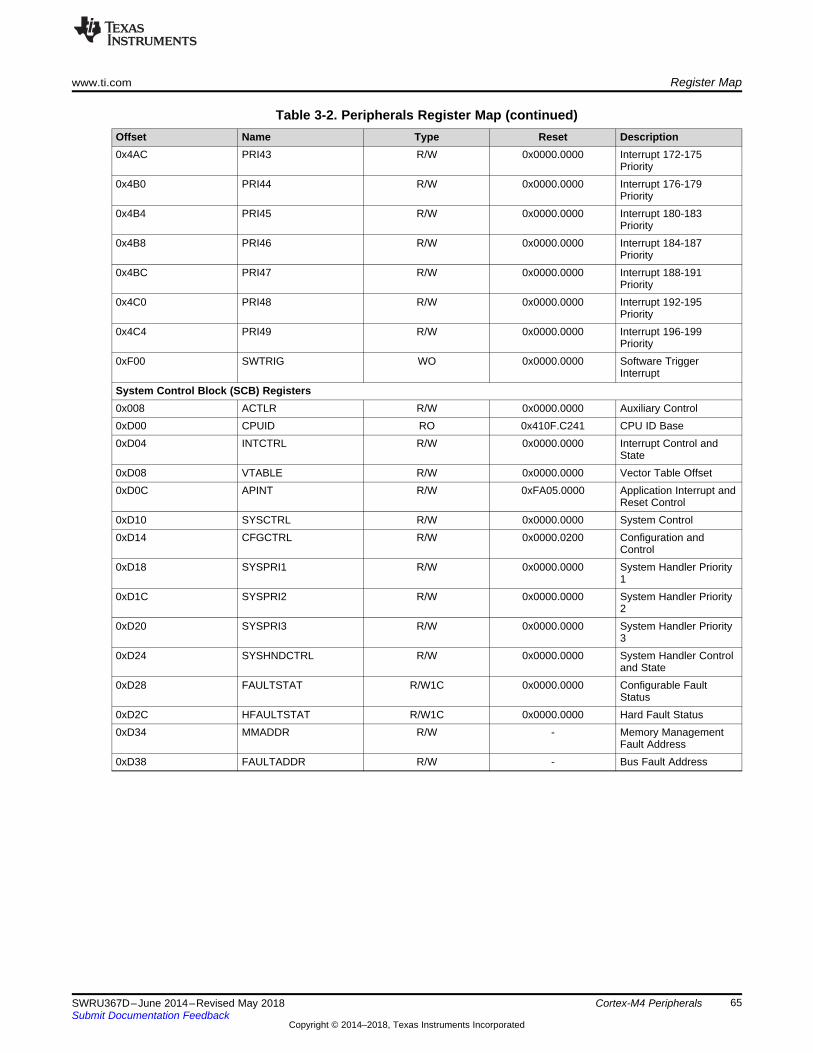
www.ti.com Register Map
65SWRU367D–June 2014–Revised May 2018Submit Documentation Feedback
Copyright © 2014–2018, Texas Instruments Incorporated
Cortex-M4 Peripherals
Table 3-2. Peripherals Register Map (continued)Offset Name Type Reset Description0x4AC PRI43 R/W 0x0000.0000 Interrupt 172-175
Priority0x4B0 PRI44 R/W 0x0000.0000 Interrupt 176-179
Priority0x4B4 PRI45 R/W 0x0000.0000 Interrupt 180-183
Priority0x4B8 PRI46 R/W 0x0000.0000 Interrupt 184-187
Priority0x4BC PRI47 R/W 0x0000.0000 Interrupt 188-191
Priority0x4C0 PRI48 R/W 0x0000.0000 Interrupt 192-195
Priority0x4C4 PRI49 R/W 0x0000.0000 Interrupt 196-199
Priority0xF00 SWTRIG WO 0x0000.0000 Software Trigger
InterruptSystem Control Block (SCB) Registers0x008 ACTLR R/W 0x0000.0000 Auxiliary Control0xD00 CPUID RO 0x410F.C241 CPU ID Base0xD04 INTCTRL R/W 0x0000.0000 Interrupt Control and
State0xD08 VTABLE R/W 0x0000.0000 Vector Table Offset0xD0C APINT R/W 0xFA05.0000 Application Interrupt and
Reset Control0xD10 SYSCTRL R/W 0x0000.0000 System Control0xD14 CFGCTRL R/W 0x0000.0200 Configuration and
Control0xD18 SYSPRI1 R/W 0x0000.0000 System Handler Priority
10xD1C SYSPRI2 R/W 0x0000.0000 System Handler Priority
20xD20 SYSPRI3 R/W 0x0000.0000 System Handler Priority
30xD24 SYSHNDCTRL R/W 0x0000.0000 System Handler Control
and State0xD28 FAULTSTAT R/W1C 0x0000.0000 Configurable Fault
Status0xD2C HFAULTSTAT R/W1C 0x0000.0000 Hard Fault Status0xD34 MMADDR R/W - Memory Management
Fault Address0xD38 FAULTADDR R/W - Bus Fault Address
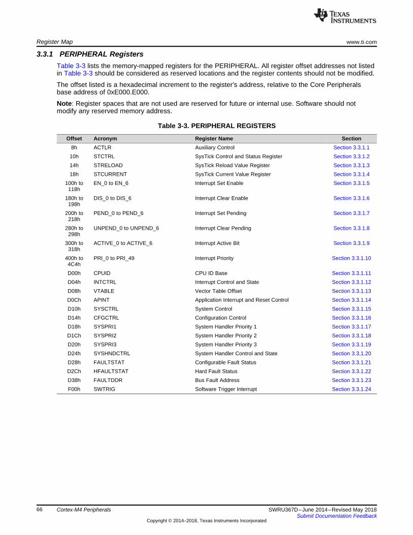
Register Map www.ti.com
66 SWRU367D–June 2014–Revised May 2018Submit Documentation Feedback
Copyright © 2014–2018, Texas Instruments Incorporated
Cortex-M4 Peripherals
3.3.1 PERIPHERAL RegistersTable 3-3 lists the memory-mapped registers for the PERIPHERAL. All register offset addresses not listedin Table 3-3 should be considered as reserved locations and the register contents should not be modified.
The offset listed is a hexadecimal increment to the register's address, relative to the Core Peripheralsbase address of 0xE000.E000.
Note: Register spaces that are not used are reserved for future or internal use. Software should notmodify any reserved memory address.
Table 3-3. PERIPHERAL REGISTERS
Offset Acronym Register Name Section8h ACTLR Auxiliary Control Section 3.3.1.110h STCTRL SysTick Control and Status Register Section 3.3.1.214h STRELOAD SysTick Reload Value Register Section 3.3.1.318h STCURRENT SysTick Current Value Register Section 3.3.1.4
100h to118h
EN_0 to EN_6 Interrupt Set Enable Section 3.3.1.5
180h to198h
DIS_0 to DIS_6 Interrupt Clear Enable Section 3.3.1.6
200h to218h
PEND_0 to PEND_6 Interrupt Set Pending Section 3.3.1.7
280h to298h
UNPEND_0 to UNPEND_6 Interrupt Clear Pending Section 3.3.1.8
300h to318h
ACTIVE_0 to ACTIVE_6 Interrupt Active Bit Section 3.3.1.9
400h to4C4h
PRI_0 to PRI_49 Interrupt Priority Section 3.3.1.10
D00h CPUID CPU ID Base Section 3.3.1.11D04h INTCTRL Interrupt Control and State Section 3.3.1.12D08h VTABLE Vector Table Offset Section 3.3.1.13D0Ch APINT Application Interrupt and Reset Control Section 3.3.1.14D10h SYSCTRL System Control Section 3.3.1.15D14h CFGCTRL Configuration Control Section 3.3.1.16D18h SYSPRI1 System Handler Priority 1 Section 3.3.1.17D1Ch SYSPRI2 System Handler Priority 2 Section 3.3.1.18D20h SYSPRI3 System Handler Priority 3 Section 3.3.1.19D24h SYSHNDCTRL System Handler Control and State Section 3.3.1.20D28h FAULTSTAT Configurable Fault Status Section 3.3.1.21D2Ch HFAULTSTAT Hard Fault Status Section 3.3.1.22D38h FAULTDDR Bus Fault Address Section 3.3.1.23F00h SWTRIG Software Trigger Interrupt Section 3.3.1.24
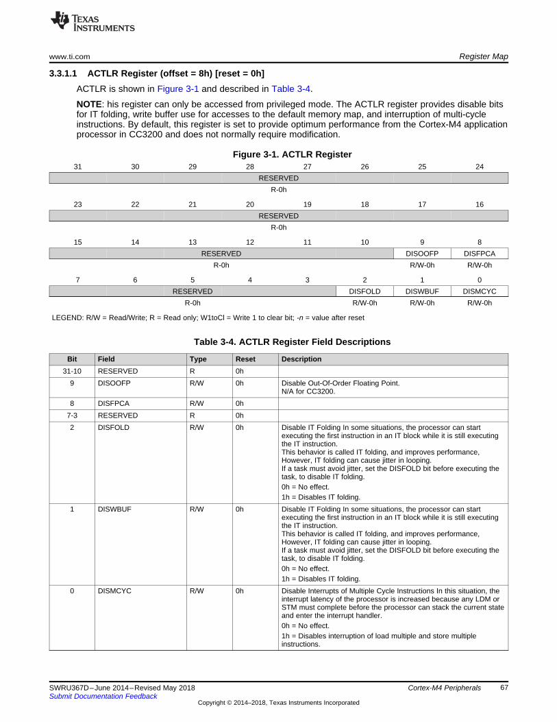
www.ti.com Register Map
67SWRU367D–June 2014–Revised May 2018Submit Documentation Feedback
Copyright © 2014–2018, Texas Instruments Incorporated
Cortex-M4 Peripherals
3.3.1.1 ACTLR Register (offset = 8h) [reset = 0h]ACTLR is shown in Figure 3-1 and described in Table 3-4.
NOTE: his register can only be accessed from privileged mode. The ACTLR register provides disable bitsfor IT folding, write buffer use for accesses to the default memory map, and interruption of multi-cycleinstructions. By default, this register is set to provide optimum performance from the Cortex-M4 applicationprocessor in CC3200 and does not normally require modification.
Figure 3-1. ACTLR Register31 30 29 28 27 26 25 24
RESERVEDR-0h
23 22 21 20 19 18 17 16RESERVED
R-0h
15 14 13 12 11 10 9 8RESERVED DISOOFP DISFPCA
R-0h R/W-0h R/W-0h
7 6 5 4 3 2 1 0RESERVED DISFOLD DISWBUF DISMCYC
R-0h R/W-0h R/W-0h R/W-0h
LEGEND: R/W = Read/Write; R = Read only; W1toCl = Write 1 to clear bit; -n = value after reset
Table 3-4. ACTLR Register Field Descriptions
Bit Field Type Reset Description31-10 RESERVED R 0h
9 DISOOFP R/W 0h Disable Out-Of-Order Floating Point.N/A for CC3200.
8 DISFPCA R/W 0h7-3 RESERVED R 0h2 DISFOLD R/W 0h Disable IT Folding In some situations, the processor can start
executing the first instruction in an IT block while it is still executingthe IT instruction.This behavior is called IT folding, and improves performance,However, IT folding can cause jitter in looping.If a task must avoid jitter, set the DISFOLD bit before executing thetask, to disable IT folding.0h = No effect.1h = Disables IT folding.
1 DISWBUF R/W 0h Disable IT Folding In some situations, the processor can startexecuting the first instruction in an IT block while it is still executingthe IT instruction.This behavior is called IT folding, and improves performance,However, IT folding can cause jitter in looping.If a task must avoid jitter, set the DISFOLD bit before executing thetask, to disable IT folding.0h = No effect.1h = Disables IT folding.
0 DISMCYC R/W 0h Disable Interrupts of Multiple Cycle Instructions In this situation, theinterrupt latency of the processor is increased because any LDM orSTM must complete before the processor can stack the current stateand enter the interrupt handler.0h = No effect.1h = Disables interruption of load multiple and store multipleinstructions.
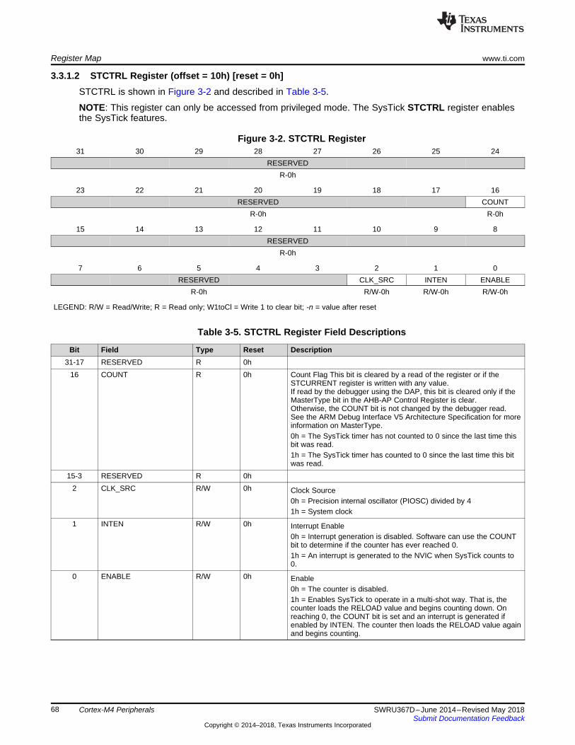
Register Map www.ti.com
68 SWRU367D–June 2014–Revised May 2018Submit Documentation Feedback
Copyright © 2014–2018, Texas Instruments Incorporated
Cortex-M4 Peripherals
3.3.1.2 STCTRL Register (offset = 10h) [reset = 0h]STCTRL is shown in Figure 3-2 and described in Table 3-5.
NOTE: This register can only be accessed from privileged mode. The SysTick STCTRL register enablesthe SysTick features.
Figure 3-2. STCTRL Register31 30 29 28 27 26 25 24
RESERVEDR-0h
23 22 21 20 19 18 17 16RESERVED COUNT
R-0h R-0h
15 14 13 12 11 10 9 8RESERVED
R-0h
7 6 5 4 3 2 1 0RESERVED CLK_SRC INTEN ENABLE
R-0h R/W-0h R/W-0h R/W-0h
LEGEND: R/W = Read/Write; R = Read only; W1toCl = Write 1 to clear bit; -n = value after reset
Table 3-5. STCTRL Register Field Descriptions
Bit Field Type Reset Description31-17 RESERVED R 0h
16 COUNT R 0h Count Flag This bit is cleared by a read of the register or if theSTCURRENT register is written with any value.If read by the debugger using the DAP, this bit is cleared only if theMasterType bit in the AHB-AP Control Register is clear.Otherwise, the COUNT bit is not changed by the debugger read.See the ARM Debug Interface V5 Architecture Specification for moreinformation on MasterType.0h = The SysTick timer has not counted to 0 since the last time thisbit was read.1h = The SysTick timer has counted to 0 since the last time this bitwas read.
15-3 RESERVED R 0h2 CLK_SRC R/W 0h Clock Source
0h = Precision internal oscillator (PIOSC) divided by 41h = System clock
1 INTEN R/W 0h Interrupt Enable0h = Interrupt generation is disabled. Software can use the COUNTbit to determine if the counter has ever reached 0.1h = An interrupt is generated to the NVIC when SysTick counts to0.
0 ENABLE R/W 0h Enable0h = The counter is disabled.1h = Enables SysTick to operate in a multi-shot way. That is, thecounter loads the RELOAD value and begins counting down. Onreaching 0, the COUNT bit is set and an interrupt is generated ifenabled by INTEN. The counter then loads the RELOAD value againand begins counting.
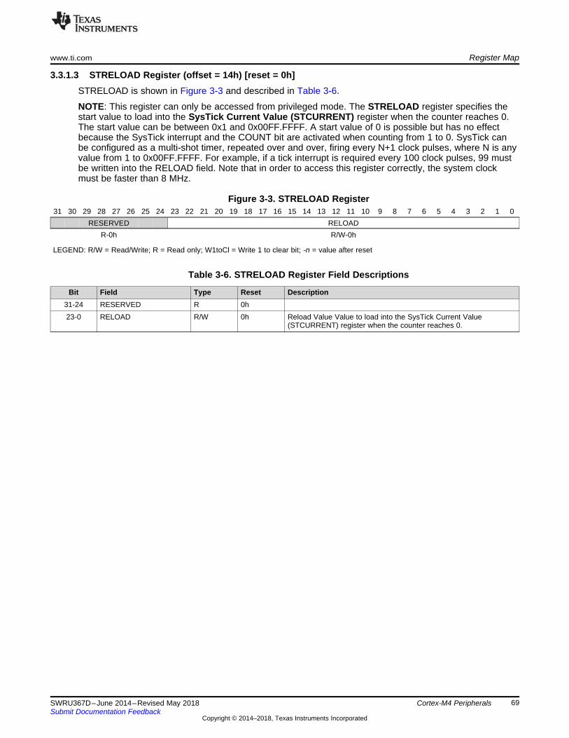
www.ti.com Register Map
69SWRU367D–June 2014–Revised May 2018Submit Documentation Feedback
Copyright © 2014–2018, Texas Instruments Incorporated
Cortex-M4 Peripherals
3.3.1.3 STRELOAD Register (offset = 14h) [reset = 0h]STRELOAD is shown in Figure 3-3 and described in Table 3-6.
NOTE: This register can only be accessed from privileged mode. The STRELOAD register specifies thestart value to load into the SysTick Current Value (STCURRENT) register when the counter reaches 0.The start value can be between 0x1 and 0x00FF.FFFF. A start value of 0 is possible but has no effectbecause the SysTick interrupt and the COUNT bit are activated when counting from 1 to 0. SysTick canbe configured as a multi-shot timer, repeated over and over, firing every N+1 clock pulses, where N is anyvalue from 1 to 0x00FF.FFFF. For example, if a tick interrupt is required every 100 clock pulses, 99 mustbe written into the RELOAD field. Note that in order to access this register correctly, the system clockmust be faster than 8 MHz.
Figure 3-3. STRELOAD Register31 30 29 28 27 26 25 24 23 22 21 20 19 18 17 16 15 14 13 12 11 10 9 8 7 6 5 4 3 2 1 0
RESERVED RELOADR-0h R/W-0h
LEGEND: R/W = Read/Write; R = Read only; W1toCl = Write 1 to clear bit; -n = value after reset
Table 3-6. STRELOAD Register Field Descriptions
Bit Field Type Reset Description31-24 RESERVED R 0h23-0 RELOAD R/W 0h Reload Value Value to load into the SysTick Current Value
(STCURRENT) register when the counter reaches 0.
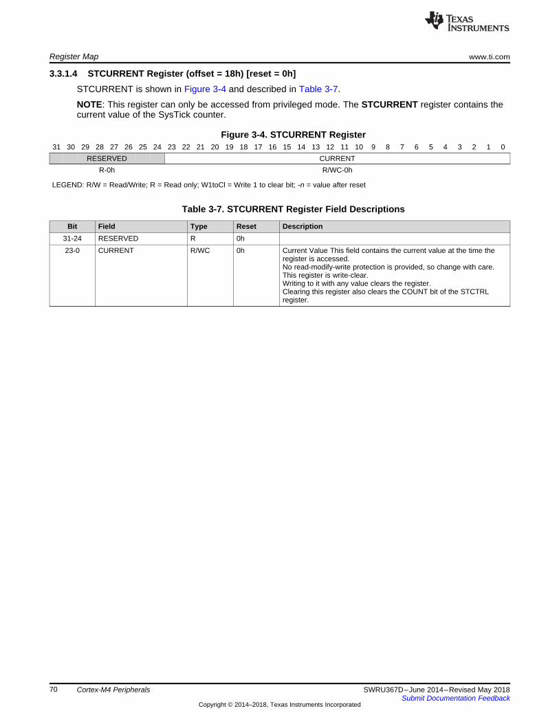
Register Map www.ti.com
70 SWRU367D–June 2014–Revised May 2018Submit Documentation Feedback
Copyright © 2014–2018, Texas Instruments Incorporated
Cortex-M4 Peripherals
3.3.1.4 STCURRENT Register (offset = 18h) [reset = 0h]STCURRENT is shown in Figure 3-4 and described in Table 3-7.
NOTE: This register can only be accessed from privileged mode. The STCURRENT register contains thecurrent value of the SysTick counter.
Figure 3-4. STCURRENT Register31 30 29 28 27 26 25 24 23 22 21 20 19 18 17 16 15 14 13 12 11 10 9 8 7 6 5 4 3 2 1 0
RESERVED CURRENTR-0h R/WC-0h
LEGEND: R/W = Read/Write; R = Read only; W1toCl = Write 1 to clear bit; -n = value after reset
Table 3-7. STCURRENT Register Field Descriptions
Bit Field Type Reset Description31-24 RESERVED R 0h23-0 CURRENT R/WC 0h Current Value This field contains the current value at the time the
register is accessed.No read-modify-write protection is provided, so change with care.This register is write-clear.Writing to it with any value clears the register.Clearing this register also clears the COUNT bit of the STCTRLregister.
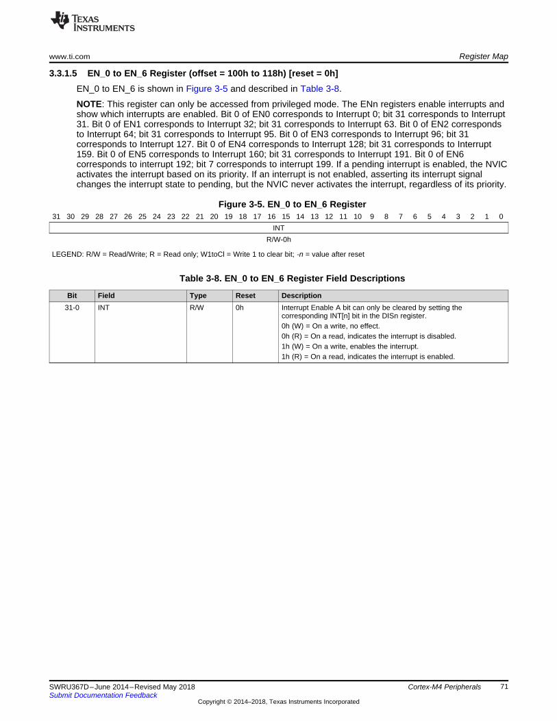
www.ti.com Register Map
71SWRU367D–June 2014–Revised May 2018Submit Documentation Feedback
Copyright © 2014–2018, Texas Instruments Incorporated
Cortex-M4 Peripherals
3.3.1.5 EN_0 to EN_6 Register (offset = 100h to 118h) [reset = 0h]EN_0 to EN_6 is shown in Figure 3-5 and described in Table 3-8.
NOTE: This register can only be accessed from privileged mode. The ENn registers enable interrupts andshow which interrupts are enabled. Bit 0 of EN0 corresponds to Interrupt 0; bit 31 corresponds to Interrupt31. Bit 0 of EN1 corresponds to Interrupt 32; bit 31 corresponds to Interrupt 63. Bit 0 of EN2 correspondsto Interrupt 64; bit 31 corresponds to Interrupt 95. Bit 0 of EN3 corresponds to Interrupt 96; bit 31corresponds to Interrupt 127. Bit 0 of EN4 corresponds to Interrupt 128; bit 31 corresponds to Interrupt159. Bit 0 of EN5 corresponds to Interrupt 160; bit 31 corresponds to Interrupt 191. Bit 0 of EN6corresponds to interrupt 192; bit 7 corresponds to interrupt 199. If a pending interrupt is enabled, the NVICactivates the interrupt based on its priority. If an interrupt is not enabled, asserting its interrupt signalchanges the interrupt state to pending, but the NVIC never activates the interrupt, regardless of its priority.
Figure 3-5. EN_0 to EN_6 Register31 30 29 28 27 26 25 24 23 22 21 20 19 18 17 16 15 14 13 12 11 10 9 8 7 6 5 4 3 2 1 0
INTR/W-0h
LEGEND: R/W = Read/Write; R = Read only; W1toCl = Write 1 to clear bit; -n = value after reset
Table 3-8. EN_0 to EN_6 Register Field Descriptions
Bit Field Type Reset Description31-0 INT R/W 0h Interrupt Enable A bit can only be cleared by setting the
corresponding INT[n] bit in the DISn register.0h (W) = On a write, no effect.0h (R) = On a read, indicates the interrupt is disabled.1h (W) = On a write, enables the interrupt.1h (R) = On a read, indicates the interrupt is enabled.
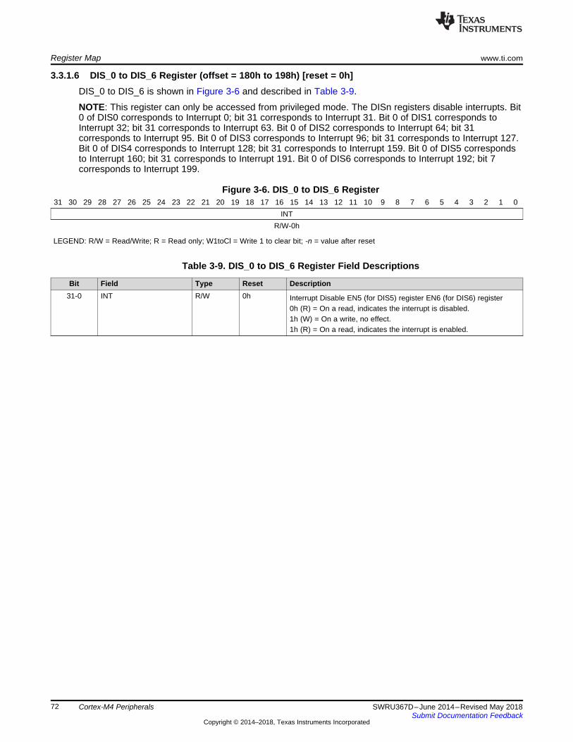
Register Map www.ti.com
72 SWRU367D–June 2014–Revised May 2018Submit Documentation Feedback
Copyright © 2014–2018, Texas Instruments Incorporated
Cortex-M4 Peripherals
3.3.1.6 DIS_0 to DIS_6 Register (offset = 180h to 198h) [reset = 0h]DIS_0 to DIS_6 is shown in Figure 3-6 and described in Table 3-9.
NOTE: This register can only be accessed from privileged mode. The DISn registers disable interrupts. Bit0 of DIS0 corresponds to Interrupt 0; bit 31 corresponds to Interrupt 31. Bit 0 of DIS1 corresponds toInterrupt 32; bit 31 corresponds to Interrupt 63. Bit 0 of DIS2 corresponds to Interrupt 64; bit 31corresponds to Interrupt 95. Bit 0 of DIS3 corresponds to Interrupt 96; bit 31 corresponds to Interrupt 127.Bit 0 of DIS4 corresponds to Interrupt 128; bit 31 corresponds to Interrupt 159. Bit 0 of DIS5 correspondsto Interrupt 160; bit 31 corresponds to Interrupt 191. Bit 0 of DIS6 corresponds to Interrupt 192; bit 7corresponds to Interrupt 199.
Figure 3-6. DIS_0 to DIS_6 Register31 30 29 28 27 26 25 24 23 22 21 20 19 18 17 16 15 14 13 12 11 10 9 8 7 6 5 4 3 2 1 0
INTR/W-0h
LEGEND: R/W = Read/Write; R = Read only; W1toCl = Write 1 to clear bit; -n = value after reset
Table 3-9. DIS_0 to DIS_6 Register Field Descriptions
Bit Field Type Reset Description31-0 INT R/W 0h Interrupt Disable EN5 (for DIS5) register EN6 (for DIS6) register
0h (R) = On a read, indicates the interrupt is disabled.1h (W) = On a write, no effect.1h (R) = On a read, indicates the interrupt is enabled.
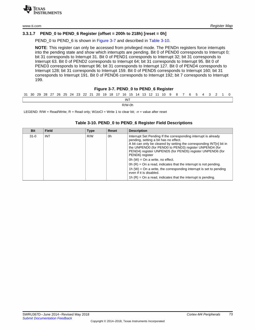
www.ti.com Register Map
73SWRU367D–June 2014–Revised May 2018Submit Documentation Feedback
Copyright © 2014–2018, Texas Instruments Incorporated
Cortex-M4 Peripherals
3.3.1.7 PEND_0 to PEND_6 Register (offset = 200h to 218h) [reset = 0h]PEND_0 to PEND_6 is shown in Figure 3-7 and described in Table 3-10.
NOTE: This register can only be accessed from privileged mode. The PENDn registers force interruptsinto the pending state and show which interrupts are pending. Bit 0 of PEND0 corresponds to Interrupt 0;bit 31 corresponds to Interrupt 31. Bit 0 of PEND1 corresponds to Interrupt 32; bit 31 corresponds toInterrupt 63. Bit 0 of PEND2 corresponds to Interrupt 64; bit 31 corresponds to Interrupt 95. Bit 0 ofPEND3 corresponds to Interrupt 96; bit 31 corresponds to Interrupt 127. Bit 0 of PEND4 corresponds toInterrupt 128; bit 31 corresponds to Interrupt 159. Bit 0 of PEND5 corresponds to Interrupt 160; bit 31corresponds to Interrupt 191. Bit 0 of PEND6 corresponds to Interrupt 192; bit 7 corresponds to Interrupt199.
Figure 3-7. PEND_0 to PEND_6 Register31 30 29 28 27 26 25 24 23 22 21 20 19 18 17 16 15 14 13 12 11 10 9 8 7 6 5 4 3 2 1 0
INTR/W-0h
LEGEND: R/W = Read/Write; R = Read only; W1toCl = Write 1 to clear bit; -n = value after reset
Table 3-10. PEND_0 to PEND_6 Register Field Descriptions
Bit Field Type Reset Description31-0 INT R/W 0h Interrupt Set Pending If the corresponding interrupt is already
pending, setting a bit has no effect.A bit can only be cleared by setting the corresponding INT[n] bit inthe UNPEND0 (for PEND0 to PEND3) register UNPEND4 (forPEND4) register UNPEND5 (for PEND5) register UNPEND6 (forPEND6) register0h (W) = On a write, no effect.0h (R) = On a read, indicates that the interrupt is not pending.1h (W) = On a write, the corresponding interrupt is set to pendingeven if it is disabled.1h (R) = On a read, indicates that the interrupt is pending.

Register Map www.ti.com
74 SWRU367D–June 2014–Revised May 2018Submit Documentation Feedback
Copyright © 2014–2018, Texas Instruments Incorporated
Cortex-M4 Peripherals
3.3.1.8 UNPEND_0 to UNPEND_6 Register (offset = 280h to 298h) [reset = 0h]UNPEND_0 to UNPEND_6 is shown in Figure 3-8 and described in Table 3-11.
NOTE: This register can only be accessed from privileged mode. The UNPENDn registers show whichinterrupts are pending and remove the pending state from interrupts. Bit 0 of UNPEND0 corresponds toInterrupt 0; bit 31 corresponds to Interrupt 31. Bit 0 of UNPEND1 corresponds to Interrupt 32; bit 31corresponds to Interrupt 63. Bit 0 of UNPEND2 corresponds to Interrupt 64; bit 31 corresponds to Interrupt95. Bit 0 of UNPEND3 corresponds to Interrupt 96; bit 31 corresponds to Interrupt 127. Bit 0 of UNPEND4corresponds to Interrupt 128; bit 10 corresponds to Interrupt 159. Bit 0 of UNPEND5 corresponds toInterrupt 160; bit 31 corresponds to interrupt 191. Bit 0 of UNPEND6 corresponds to Interrupt 192; bit 7corresponds to Interrupt 199.
Figure 3-8. UNPEND_0 to UNPEND_6 Register31 30 29 28 27 26 25 24 23 22 21 20 19 18 17 16 15 14 13 12 11 10 9 8 7 6 5 4 3 2 1 0
INTR/W-0h
LEGEND: R/W = Read/Write; R = Read only; W1toCl = Write 1 to clear bit; -n = value after reset
Table 3-11. UNPEND_0 to UNPEND_6 Register Field Descriptions
Bit Field Type Reset Description31-0 INT R/W 0h Interrupt Clear Pending Setting a bit does not affect the active state
of the corresponding interrupt.0h (W) = On a write, no effect.0h (R) = On a read, indicates that the interrupt is not pending.1h (W) = On a write, clears the corresponding INT[n] bit in thePEND0 (for UNPEND0 to UNPEND3) register PEND4 (forUNPEND4) register PEND5 (for UNPEND5) register PEND6 (forUNPEND6) register so that interrupt [n] is no longer pending.1h (R) = On a read, indicates that the interrupt is pending.
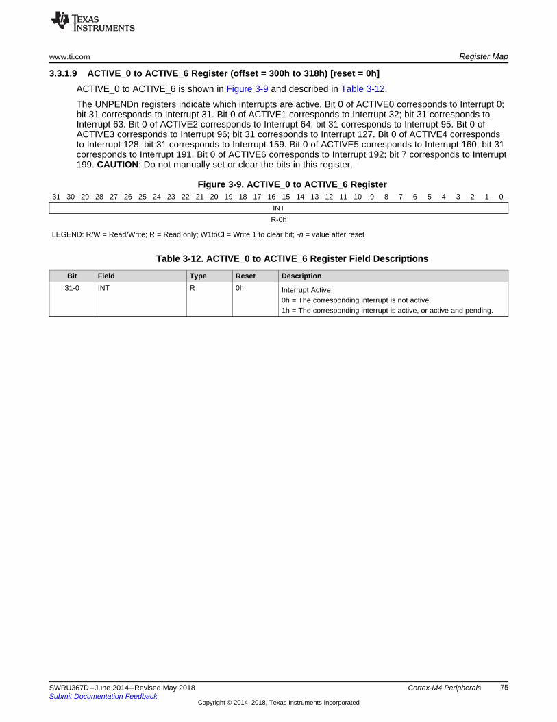
www.ti.com Register Map
75SWRU367D–June 2014–Revised May 2018Submit Documentation Feedback
Copyright © 2014–2018, Texas Instruments Incorporated
Cortex-M4 Peripherals
3.3.1.9 ACTIVE_0 to ACTIVE_6 Register (offset = 300h to 318h) [reset = 0h]ACTIVE_0 to ACTIVE_6 is shown in Figure 3-9 and described in Table 3-12.
The UNPENDn registers indicate which interrupts are active. Bit 0 of ACTIVE0 corresponds to Interrupt 0;bit 31 corresponds to Interrupt 31. Bit 0 of ACTIVE1 corresponds to Interrupt 32; bit 31 corresponds toInterrupt 63. Bit 0 of ACTIVE2 corresponds to Interrupt 64; bit 31 corresponds to Interrupt 95. Bit 0 ofACTIVE3 corresponds to Interrupt 96; bit 31 corresponds to Interrupt 127. Bit 0 of ACTIVE4 correspondsto Interrupt 128; bit 31 corresponds to Interrupt 159. Bit 0 of ACTIVE5 corresponds to Interrupt 160; bit 31corresponds to Interrupt 191. Bit 0 of ACTIVE6 corresponds to Interrupt 192; bit 7 corresponds to Interrupt199. CAUTION: Do not manually set or clear the bits in this register.
Figure 3-9. ACTIVE_0 to ACTIVE_6 Register31 30 29 28 27 26 25 24 23 22 21 20 19 18 17 16 15 14 13 12 11 10 9 8 7 6 5 4 3 2 1 0
INTR-0h
LEGEND: R/W = Read/Write; R = Read only; W1toCl = Write 1 to clear bit; -n = value after reset
Table 3-12. ACTIVE_0 to ACTIVE_6 Register Field Descriptions
Bit Field Type Reset Description31-0 INT R 0h Interrupt Active
0h = The corresponding interrupt is not active.1h = The corresponding interrupt is active, or active and pending.
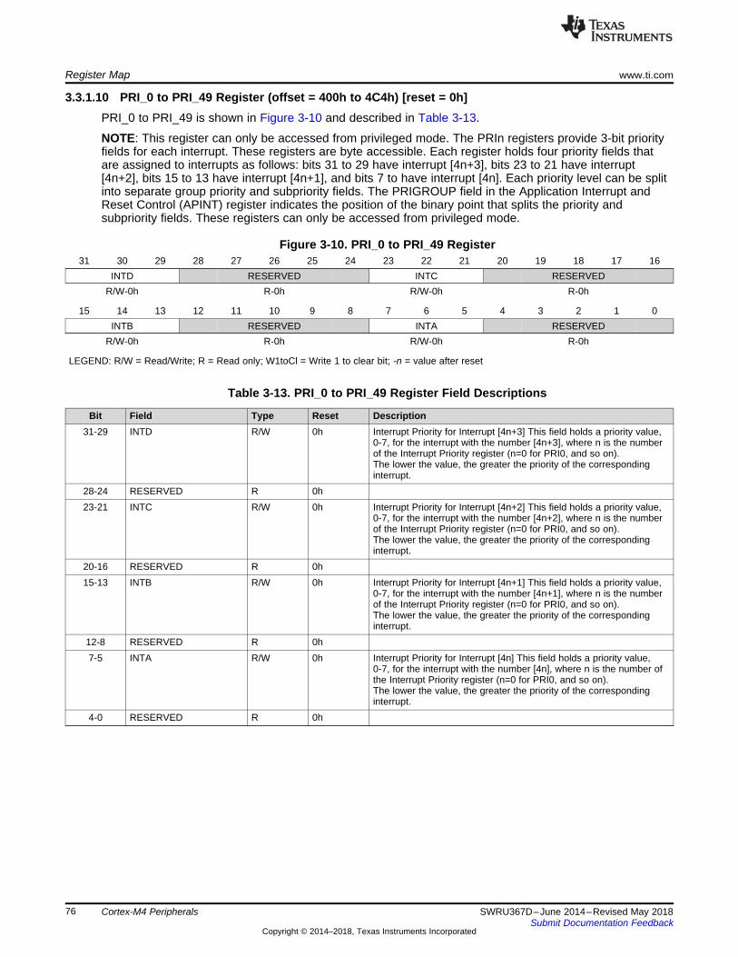
Register Map www.ti.com
76 SWRU367D–June 2014–Revised May 2018Submit Documentation Feedback
Copyright © 2014–2018, Texas Instruments Incorporated
Cortex-M4 Peripherals
3.3.1.10 PRI_0 to PRI_49 Register (offset = 400h to 4C4h) [reset = 0h]PRI_0 to PRI_49 is shown in Figure 3-10 and described in Table 3-13.
NOTE: This register can only be accessed from privileged mode. The PRIn registers provide 3-bit priorityfields for each interrupt. These registers are byte accessible. Each register holds four priority fields thatare assigned to interrupts as follows: bits 31 to 29 have interrupt [4n+3], bits 23 to 21 have interrupt[4n+2], bits 15 to 13 have interrupt [4n+1], and bits 7 to have interrupt [4n]. Each priority level can be splitinto separate group priority and subpriority fields. The PRIGROUP field in the Application Interrupt andReset Control (APINT) register indicates the position of the binary point that splits the priority andsubpriority fields. These registers can only be accessed from privileged mode.
Figure 3-10. PRI_0 to PRI_49 Register31 30 29 28 27 26 25 24 23 22 21 20 19 18 17 16
INTD RESERVED INTC RESERVEDR/W-0h R-0h R/W-0h R-0h
15 14 13 12 11 10 9 8 7 6 5 4 3 2 1 0INTB RESERVED INTA RESERVED
R/W-0h R-0h R/W-0h R-0h
LEGEND: R/W = Read/Write; R = Read only; W1toCl = Write 1 to clear bit; -n = value after reset
Table 3-13. PRI_0 to PRI_49 Register Field Descriptions
Bit Field Type Reset Description31-29 INTD R/W 0h Interrupt Priority for Interrupt [4n+3] This field holds a priority value,
0-7, for the interrupt with the number [4n+3], where n is the numberof the Interrupt Priority register (n=0 for PRI0, and so on).The lower the value, the greater the priority of the correspondinginterrupt.
28-24 RESERVED R 0h23-21 INTC R/W 0h Interrupt Priority for Interrupt [4n+2] This field holds a priority value,
0-7, for the interrupt with the number [4n+2], where n is the numberof the Interrupt Priority register (n=0 for PRI0, and so on).The lower the value, the greater the priority of the correspondinginterrupt.
20-16 RESERVED R 0h15-13 INTB R/W 0h Interrupt Priority for Interrupt [4n+1] This field holds a priority value,
0-7, for the interrupt with the number [4n+1], where n is the numberof the Interrupt Priority register (n=0 for PRI0, and so on).The lower the value, the greater the priority of the correspondinginterrupt.
12-8 RESERVED R 0h7-5 INTA R/W 0h Interrupt Priority for Interrupt [4n] This field holds a priority value,
0-7, for the interrupt with the number [4n], where n is the number ofthe Interrupt Priority register (n=0 for PRI0, and so on).The lower the value, the greater the priority of the correspondinginterrupt.
4-0 RESERVED R 0h
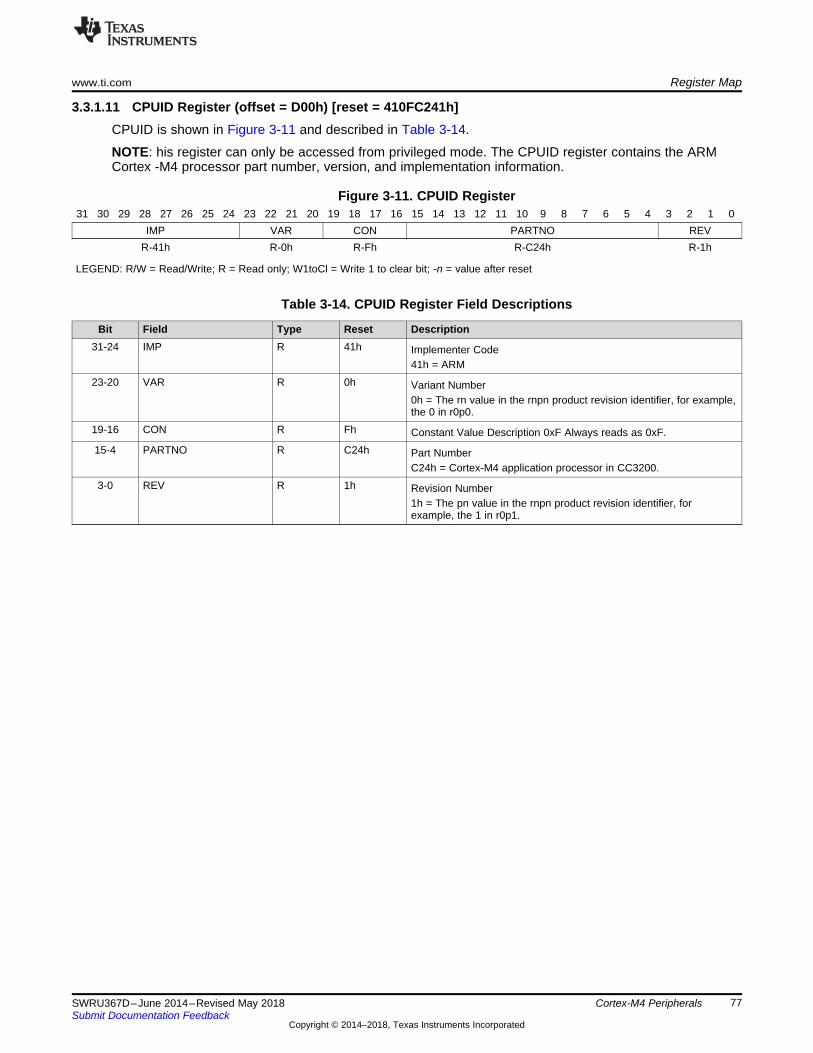
www.ti.com Register Map
77SWRU367D–June 2014–Revised May 2018Submit Documentation Feedback
Copyright © 2014–2018, Texas Instruments Incorporated
Cortex-M4 Peripherals
3.3.1.11 CPUID Register (offset = D00h) [reset = 410FC241h]CPUID is shown in Figure 3-11 and described in Table 3-14.
NOTE: his register can only be accessed from privileged mode. The CPUID register contains the ARMCortex -M4 processor part number, version, and implementation information.
Figure 3-11. CPUID Register31 30 29 28 27 26 25 24 23 22 21 20 19 18 17 16 15 14 13 12 11 10 9 8 7 6 5 4 3 2 1 0
IMP VAR CON PARTNO REVR-41h R-0h R-Fh R-C24h R-1h
LEGEND: R/W = Read/Write; R = Read only; W1toCl = Write 1 to clear bit; -n = value after reset
Table 3-14. CPUID Register Field Descriptions
Bit Field Type Reset Description31-24 IMP R 41h Implementer Code
41h = ARM23-20 VAR R 0h Variant Number
0h = The rn value in the rnpn product revision identifier, for example,the 0 in r0p0.
19-16 CON R Fh Constant Value Description 0xF Always reads as 0xF.15-4 PARTNO R C24h Part Number
C24h = Cortex-M4 application processor in CC3200.3-0 REV R 1h Revision Number
1h = The pn value in the rnpn product revision identifier, forexample, the 1 in r0p1.
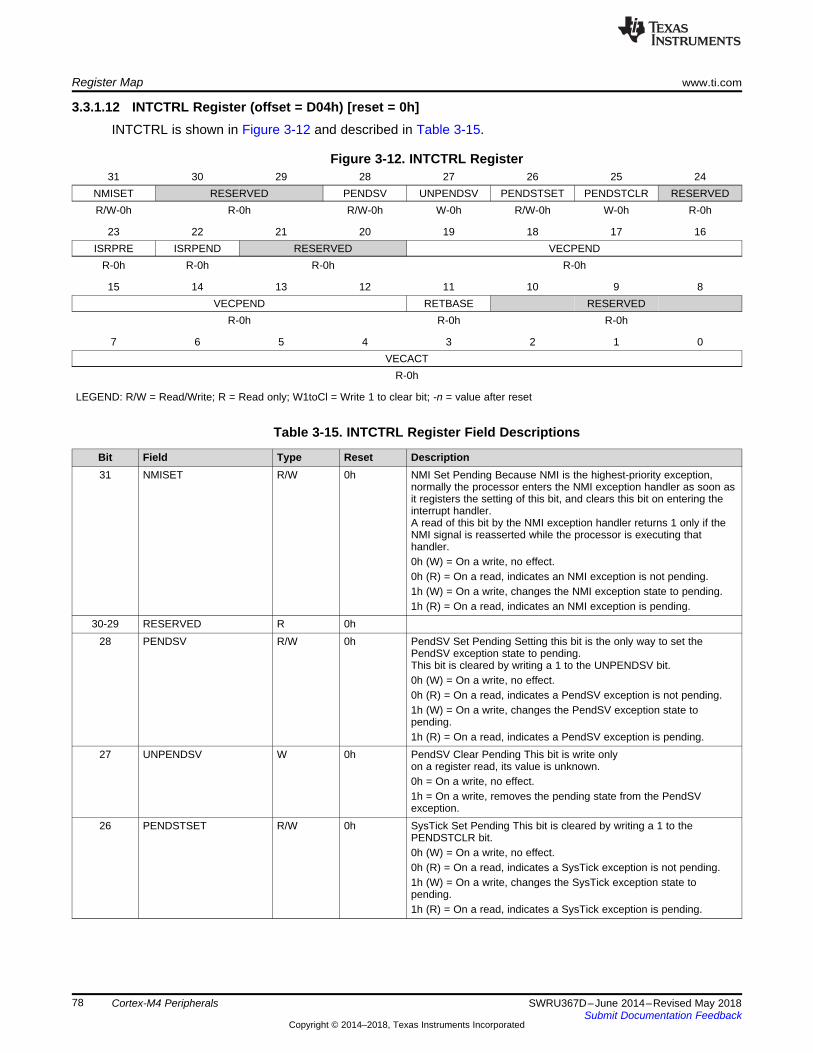
Register Map www.ti.com
78 SWRU367D–June 2014–Revised May 2018Submit Documentation Feedback
Copyright © 2014–2018, Texas Instruments Incorporated
Cortex-M4 Peripherals
3.3.1.12 INTCTRL Register (offset = D04h) [reset = 0h]INTCTRL is shown in Figure 3-12 and described in Table 3-15.
Figure 3-12. INTCTRL Register31 30 29 28 27 26 25 24
NMISET RESERVED PENDSV UNPENDSV PENDSTSET PENDSTCLR RESERVEDR/W-0h R-0h R/W-0h W-0h R/W-0h W-0h R-0h
23 22 21 20 19 18 17 16ISRPRE ISRPEND RESERVED VECPEND
R-0h R-0h R-0h R-0h
15 14 13 12 11 10 9 8VECPEND RETBASE RESERVED
R-0h R-0h R-0h
7 6 5 4 3 2 1 0VECACT
R-0h
LEGEND: R/W = Read/Write; R = Read only; W1toCl = Write 1 to clear bit; -n = value after reset
Table 3-15. INTCTRL Register Field Descriptions
Bit Field Type Reset Description31 NMISET R/W 0h NMI Set Pending Because NMI is the highest-priority exception,
normally the processor enters the NMI exception handler as soon asit registers the setting of this bit, and clears this bit on entering theinterrupt handler.A read of this bit by the NMI exception handler returns 1 only if theNMI signal is reasserted while the processor is executing thathandler.0h (W) = On a write, no effect.0h (R) = On a read, indicates an NMI exception is not pending.1h (W) = On a write, changes the NMI exception state to pending.1h (R) = On a read, indicates an NMI exception is pending.
30-29 RESERVED R 0h28 PENDSV R/W 0h PendSV Set Pending Setting this bit is the only way to set the
PendSV exception state to pending.This bit is cleared by writing a 1 to the UNPENDSV bit.0h (W) = On a write, no effect.0h (R) = On a read, indicates a PendSV exception is not pending.1h (W) = On a write, changes the PendSV exception state topending.1h (R) = On a read, indicates a PendSV exception is pending.
27 UNPENDSV W 0h PendSV Clear Pending This bit is write onlyon a register read, its value is unknown.0h = On a write, no effect.1h = On a write, removes the pending state from the PendSVexception.
26 PENDSTSET R/W 0h SysTick Set Pending This bit is cleared by writing a 1 to thePENDSTCLR bit.0h (W) = On a write, no effect.0h (R) = On a read, indicates a SysTick exception is not pending.1h (W) = On a write, changes the SysTick exception state topending.1h (R) = On a read, indicates a SysTick exception is pending.

www.ti.com Register Map
79SWRU367D–June 2014–Revised May 2018Submit Documentation Feedback
Copyright © 2014–2018, Texas Instruments Incorporated
Cortex-M4 Peripherals
Table 3-15. INTCTRL Register Field Descriptions (continued)Bit Field Type Reset Description25 PENDSTCLR W 0h SysTick Clear Pending This bit is write only
on a register read, its value is unknown.0h = On a write, no effect.1h = On a write, removes the pending state from the SysTickexception.
24 RESERVED R 0h23 ISRPRE R 0h Debug Interrupt Handling This bit is only meaningful in Debug mode
and reads as zero when the processor is not in Debug mode.0h = The release from halt does not take an interrupt.1h = The release from halt takes an interrupt.
22 ISRPEND R 0h Interrupt Pending This bit provides status for all interrupts excludingNMI and Faults.0h = No interrupt is pending.1h = An interrupt is pending.
21-20 RESERVED R 0h19-12 VECPEND R 0h Interrupt Pending Vector Number This field contains the exception
number of the highest priority pending enabled exception.The value indicated by this field includes the effect of the BASEPRIand FAULTMASK registers, but not any effect of the PRIMASKregister.7h- Ah = Reserved ...0h = No exceptions are pending1h = Reserved2h = NMI3h = Hard fault4h = Memory management fault5h = Bus fault6h = Usage faultBh = SVCallCh = Reserved for DebugDh = ReservedEh = PendSVFh = SysTick10h = Interrupt Vector 011h = Interrupt Vector 1D9h = Interrupt Vector 199
11 RETBASE R 0h Return to Base This bit provides status for all interrupts excludingNMI and Faults.This bit only has meaning if the processor is currently executing anISR (the Interrupt Program Status (IPSR) register is non-zero).0h = There are preempted active exceptions to execute.1h = There are no active exceptions, or the currently executingexception is the only active exception.
10-8 RESERVED R 0h7-0 VECACT R 0h Interrupt Pending Vector Number This field contains the active
exception number.The exception numbers can be found in the description for theVECPEND field.If this field is clear, the processor is in Thread mode.This field contains the same value as the ISRNUM field in the IPSRregister.Subtract 16 from this value to obtain the IRQ number required toindex into the Interrupt Set Enable (ENn), Interrupt Clear Enable(DISn), Interrupt Set Pending (PENDn), Interrupt Clear Pending(UNPENDn), and Interrupt Priority (PRIn) registers.
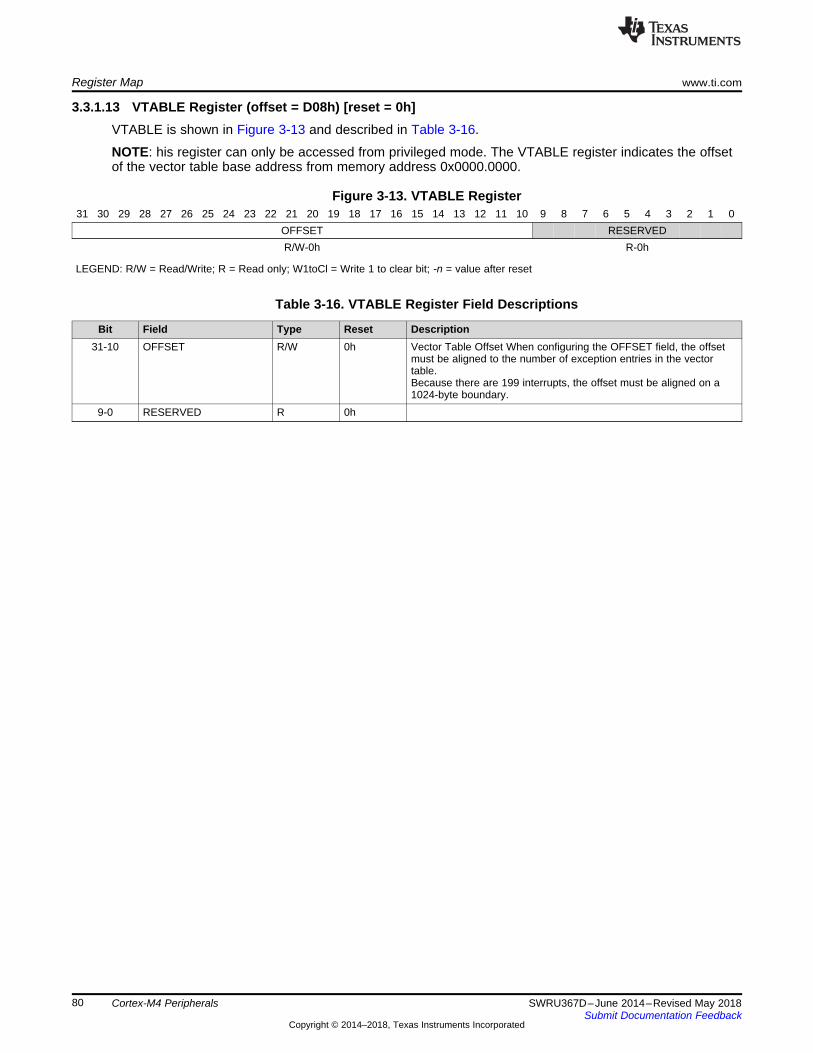
Register Map www.ti.com
80 SWRU367D–June 2014–Revised May 2018Submit Documentation Feedback
Copyright © 2014–2018, Texas Instruments Incorporated
Cortex-M4 Peripherals
3.3.1.13 VTABLE Register (offset = D08h) [reset = 0h]VTABLE is shown in Figure 3-13 and described in Table 3-16.
NOTE: his register can only be accessed from privileged mode. The VTABLE register indicates the offsetof the vector table base address from memory address 0x0000.0000.
Figure 3-13. VTABLE Register31 30 29 28 27 26 25 24 23 22 21 20 19 18 17 16 15 14 13 12 11 10 9 8 7 6 5 4 3 2 1 0
OFFSET RESERVEDR/W-0h R-0h
LEGEND: R/W = Read/Write; R = Read only; W1toCl = Write 1 to clear bit; -n = value after reset
Table 3-16. VTABLE Register Field Descriptions
Bit Field Type Reset Description31-10 OFFSET R/W 0h Vector Table Offset When configuring the OFFSET field, the offset
must be aligned to the number of exception entries in the vectortable.Because there are 199 interrupts, the offset must be aligned on a1024-byte boundary.
9-0 RESERVED R 0h
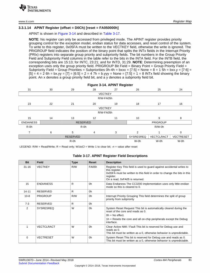
www.ti.com Register Map
81SWRU367D–June 2014–Revised May 2018Submit Documentation Feedback
Copyright © 2014–2018, Texas Instruments Incorporated
Cortex-M4 Peripherals
3.3.1.14 APINT Register (offset = D0Ch) [reset = FA050000h]APINT is shown in Figure 3-14 and described in Table 3-17.
NOTE: his register can only be accessed from privileged mode. The APINT register provides prioritygrouping control for the exception model, endian status for data accesses, and reset control of the system.To write to this register, 0x05FA must be written to the VECTKEY field, otherwise the write is ignored. ThePRIGROUP field indicates the position of the binary point that splits the INTx fields in the Interrupt Priority(PRIx) registers into separate group priority and subpriority fields. The bit numbers in the Group PriorityField and Subpriority Field columns in the table refer to the bits in the INTA field. For the INTB field, thecorresponding bits are 15:13; for INTC, 23:21; and for INTD, 31:29. NOTE: Determining preemption of anexception uses only the group priority field. PRIGROUP Bit Field = Binary Point = Group Priority Field =Subpriority Field = Group Priorities = Subpriorities 0h-4h = bxxx = [7:5] = None = 8 = 1 5h = bxx.y = [7:6] =[5] = 4 = 2 6h = bx.yy = [7] = [6:5] = 2 = 4 7h = b.yyy = None = [7:5] = 1 = 8 INTx field showing the binarypoint. An x denotes a group priority field bit, and a y denotes a subpriority field bit.
Figure 3-14. APINT Register31 30 29 28 27 26 25 24
VECTKEYR/W-FA05h
23 22 21 20 19 18 17 16VECTKEYR/W-FA05h
15 14 13 12 11 10 9 8ENDIANESS RESERVED PRIGROUP
R-0h R-0h R/W-0h
7 6 5 4 3 2 1 0RESERVED SYSRESREQ VECTCLRACT VECTRESET
R-0h W-0h W-0h W-0h
LEGEND: R/W = Read/Write; R = Read only; W1toCl = Write 1 to clear bit; -n = value after reset
Table 3-17. APINT Register Field Descriptions
Bit Field Type Reset Description31-16 VECTKEY R/W FA05h Register Key This field is used to guard against accidental writes to
this register.0x05FA must be written to this field in order to change the bits in thisregister.On a read, 0xFA05 is returned.
15 ENDIANESS R 0h Data Endianess The CC3200 implementation uses only little-endianmode so this is cleared to 0.
14-11 RESERVED R 0h10-8 PRIGROUP R/W 0h Interrupt Priority Grouping This field determines the split of group
priority from subpriority7-3 RESERVED R 0h2 SYSRESREQ W 0h System Reset Request This bit is automatically cleared during the
reset of the core and reads as 0.0h = No effect.1h = Resets the core and all on-chip peripherals except the Debuginterface.
1 VECTCLRACT W 0h Clear Active NMI / Fault This bit is reserved for Debug use andreads as 0.This bit must be written as a 0, otherwise behavior is unpredictable.
0 VECTRESET W 0h System Reset This bit is reserved for Debug use and reads as 0.This bit must be written as a 0, otherwise behavior is unpredictable.
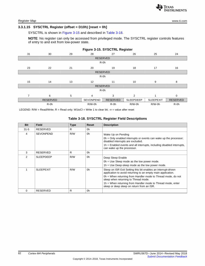
Register Map www.ti.com
82 SWRU367D–June 2014–Revised May 2018Submit Documentation Feedback
Copyright © 2014–2018, Texas Instruments Incorporated
Cortex-M4 Peripherals
3.3.1.15 SYSCTRL Register (offset = D10h) [reset = 0h]SYSCTRL is shown in Figure 3-15 and described in Table 3-18.
NOTE: his register can only be accessed from privileged mode. The SYSCTRL register controls featuresof entry to and exit from low-power state.
Figure 3-15. SYSCTRL Register31 30 29 28 27 26 25 24
RESERVEDR-0h
23 22 21 20 19 18 17 16RESERVED
R-0h
15 14 13 12 11 10 9 8RESERVED
R-0h
7 6 5 4 3 2 1 0RESERVED SEVONPEND RESERVED SLEEPDEEP SLEEPEXIT RESERVED
R-0h R/W-0h R-0h R/W-0h R/W-0h R-0h
LEGEND: R/W = Read/Write; R = Read only; W1toCl = Write 1 to clear bit; -n = value after reset
Table 3-18. SYSCTRL Register Field Descriptions
Bit Field Type Reset Description31-5 RESERVED R 0h
4 SEVONPEND R/W 0h Wake Up on Pending0h = Only enabled interrupts or events can wake up the processor;disabled interrupts are excluded.1h = Enabled events and all interrupts, including disabled interrupts,can wake up the processor.
3 RESERVED R 0h2 SLEEPDEEP R/W 0h Deep Sleep Enable
0h = Use Sleep mode as the low power mode.1h = Use Deep-sleep mode as the low power mode.
1 SLEEPEXIT R/W 0h Sleep on ISR Exit Setting this bit enables an interrupt-drivenapplication to avoid returning to an empty main application.0h = When returning from Handler mode to Thread mode, do notsleep when returning to Thread mode.1h = When returning from Handler mode to Thread mode, entersleep or deep sleep on return from an ISR.
0 RESERVED R 0h
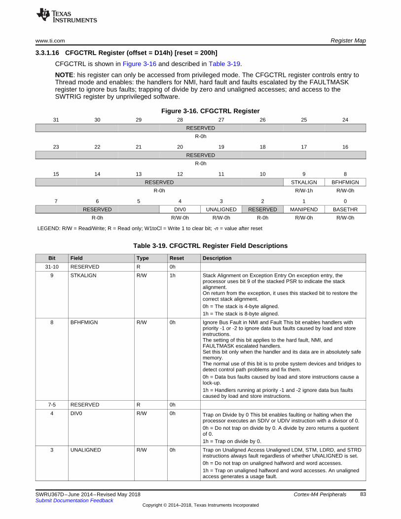
www.ti.com Register Map
83SWRU367D–June 2014–Revised May 2018Submit Documentation Feedback
Copyright © 2014–2018, Texas Instruments Incorporated
Cortex-M4 Peripherals
3.3.1.16 CFGCTRL Register (offset = D14h) [reset = 200h]CFGCTRL is shown in Figure 3-16 and described in Table 3-19.
NOTE: his register can only be accessed from privileged mode. The CFGCTRL register controls entry toThread mode and enables: the handlers for NMI, hard fault and faults escalated by the FAULTMASKregister to ignore bus faults; trapping of divide by zero and unaligned accesses; and access to theSWTRIG register by unprivileged software.
Figure 3-16. CFGCTRL Register31 30 29 28 27 26 25 24
RESERVEDR-0h
23 22 21 20 19 18 17 16RESERVED
R-0h
15 14 13 12 11 10 9 8RESERVED STKALIGN BFHFMIGN
R-0h R/W-1h R/W-0h
7 6 5 4 3 2 1 0RESERVED DIV0 UNALIGNED RESERVED MANIPEND BASETHR
R-0h R/W-0h R/W-0h R-0h R/W-0h R/W-0h
LEGEND: R/W = Read/Write; R = Read only; W1toCl = Write 1 to clear bit; -n = value after reset
Table 3-19. CFGCTRL Register Field Descriptions
Bit Field Type Reset Description31-10 RESERVED R 0h
9 STKALIGN R/W 1h Stack Alignment on Exception Entry On exception entry, theprocessor uses bit 9 of the stacked PSR to indicate the stackalignment.On return from the exception, it uses this stacked bit to restore thecorrect stack alignment.0h = The stack is 4-byte aligned.1h = The stack is 8-byte aligned.
8 BFHFMIGN R/W 0h Ignore Bus Fault in NMI and Fault This bit enables handlers withpriority -1 or -2 to ignore data bus faults caused by load and storeinstructions.The setting of this bit applies to the hard fault, NMI, andFAULTMASK escalated handlers.Set this bit only when the handler and its data are in absolutely safememory.The normal use of this bit is to probe system devices and bridges todetect control path problems and fix them.0h = Data bus faults caused by load and store instructions cause alock-up.1h = Handlers running at priority -1 and -2 ignore data bus faultscaused by load and store instructions.
7-5 RESERVED R 0h4 DIV0 R/W 0h Trap on Divide by 0 This bit enables faulting or halting when the
processor executes an SDIV or UDIV instruction with a divisor of 0.0h = Do not trap on divide by 0. A divide by zero returns a quotientof 0.1h = Trap on divide by 0.
3 UNALIGNED R/W 0h Trap on Unaligned Access Unaligned LDM, STM, LDRD, and STRDinstructions always fault regardless of whether UNALIGNED is set.0h = Do not trap on unaligned halfword and word accesses.1h = Trap on unaligned halfword and word accesses. An unalignedaccess generates a usage fault.
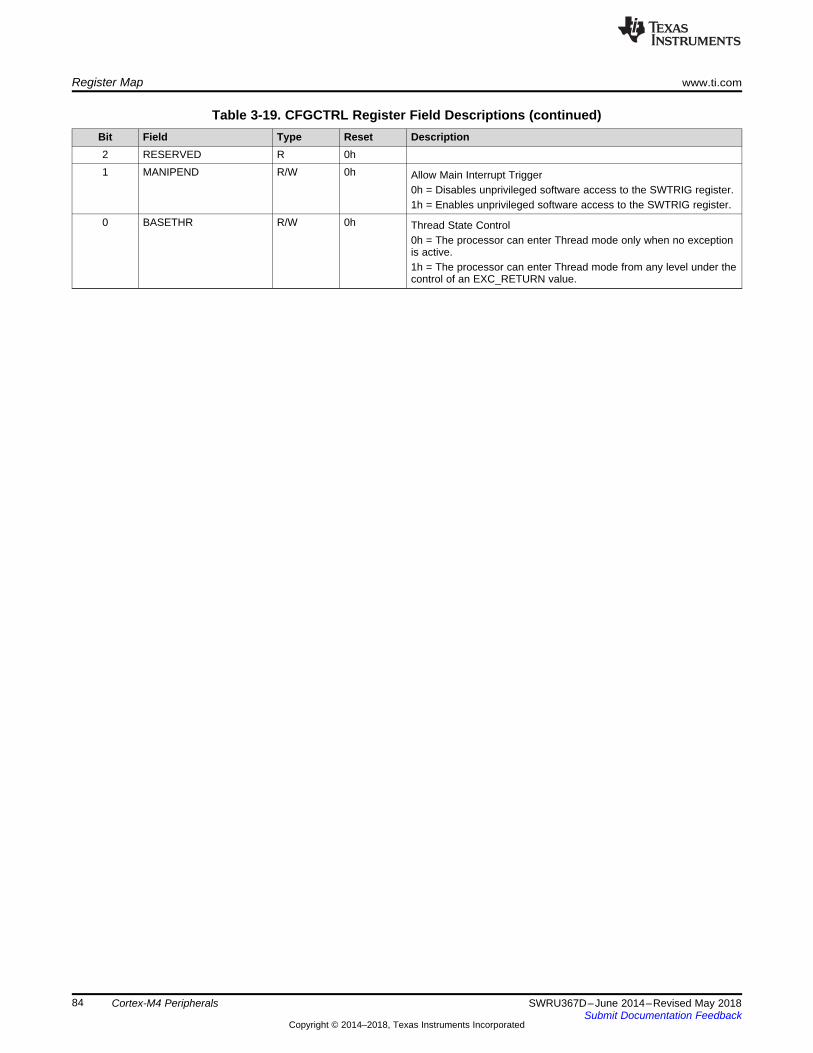
Register Map www.ti.com
84 SWRU367D–June 2014–Revised May 2018Submit Documentation Feedback
Copyright © 2014–2018, Texas Instruments Incorporated
Cortex-M4 Peripherals
Table 3-19. CFGCTRL Register Field Descriptions (continued)Bit Field Type Reset Description2 RESERVED R 0h1 MANIPEND R/W 0h Allow Main Interrupt Trigger
0h = Disables unprivileged software access to the SWTRIG register.1h = Enables unprivileged software access to the SWTRIG register.
0 BASETHR R/W 0h Thread State Control0h = The processor can enter Thread mode only when no exceptionis active.1h = The processor can enter Thread mode from any level under thecontrol of an EXC_RETURN value.
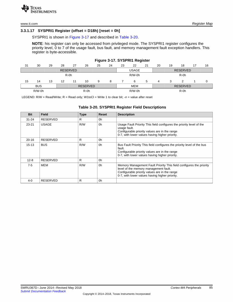
www.ti.com Register Map
85SWRU367D–June 2014–Revised May 2018Submit Documentation Feedback
Copyright © 2014–2018, Texas Instruments Incorporated
Cortex-M4 Peripherals
3.3.1.17 SYSPRI1 Register (offset = D18h) [reset = 0h]SYSPRI1 is shown in Figure 3-17 and described in Table 3-20.
NOTE: his register can only be accessed from privileged mode. The SYSPRI1 register configures thepriority level, 0 to 7 of the usage fault, bus fault, and memory management fault exception handlers. Thisregister is byte-accessible.
Figure 3-17. SYSPRI1 Register31 30 29 28 27 26 25 24 23 22 21 20 19 18 17 16
RESERVED USAGE RESERVEDR-0h R/W-0h R-0h
15 14 13 12 11 10 9 8 7 6 5 4 3 2 1 0BUS RESERVED MEM RESERVED
R/W-0h R-0h R/W-0h R-0h
LEGEND: R/W = Read/Write; R = Read only; W1toCl = Write 1 to clear bit; -n = value after reset
Table 3-20. SYSPRI1 Register Field Descriptions
Bit Field Type Reset Description31-24 RESERVED R 0h23-21 USAGE R/W 0h Usage Fault Priority This field configures the priority level of the
usage fault.Configurable priority values are in the range0-7, with lower values having higher priority.
20-16 RESERVED R 0h15-13 BUS R/W 0h Bus Fault Priority This field configures the priority level of the bus
fault.Configurable priority values are in the range0-7, with lower values having higher priority.
12-8 RESERVED R 0h7-5 MEM R/W 0h Memory Management Fault Priority This field configures the priority
level of the memory management fault.Configurable priority values are in the range0-7, with lower values having higher priority.
4-0 RESERVED R 0h
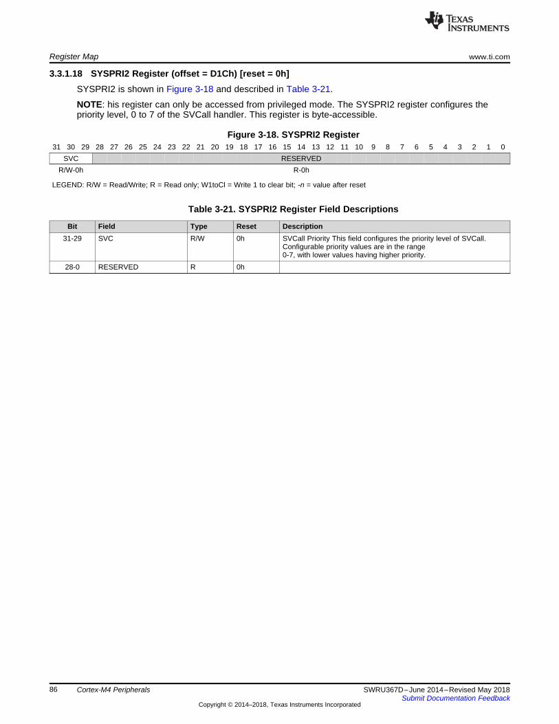
Register Map www.ti.com
86 SWRU367D–June 2014–Revised May 2018Submit Documentation Feedback
Copyright © 2014–2018, Texas Instruments Incorporated
Cortex-M4 Peripherals
3.3.1.18 SYSPRI2 Register (offset = D1Ch) [reset = 0h]SYSPRI2 is shown in Figure 3-18 and described in Table 3-21.
NOTE: his register can only be accessed from privileged mode. The SYSPRI2 register configures thepriority level, 0 to 7 of the SVCall handler. This register is byte-accessible.
Figure 3-18. SYSPRI2 Register31 30 29 28 27 26 25 24 23 22 21 20 19 18 17 16 15 14 13 12 11 10 9 8 7 6 5 4 3 2 1 0
SVC RESERVEDR/W-0h R-0h
LEGEND: R/W = Read/Write; R = Read only; W1toCl = Write 1 to clear bit; -n = value after reset
Table 3-21. SYSPRI2 Register Field Descriptions
Bit Field Type Reset Description31-29 SVC R/W 0h SVCall Priority This field configures the priority level of SVCall.
Configurable priority values are in the range0-7, with lower values having higher priority.
28-0 RESERVED R 0h
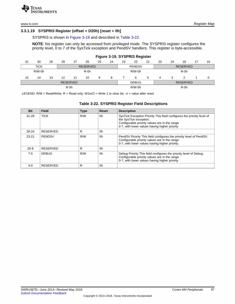
www.ti.com Register Map
87SWRU367D–June 2014–Revised May 2018Submit Documentation Feedback
Copyright © 2014–2018, Texas Instruments Incorporated
Cortex-M4 Peripherals
3.3.1.19 SYSPRI3 Register (offset = D20h) [reset = 0h]SYSPRI3 is shown in Figure 3-19 and described in Table 3-22.
NOTE: his register can only be accessed from privileged mode. The SYSPRI3 register configures thepriority level, 0 to 7 of the SysTick exception and PendSV handlers. This register is byte-accessible.
Figure 3-19. SYSPRI3 Register31 30 29 28 27 26 25 24 23 22 21 20 19 18 17 16
TICK RESERVED PENDSV RESERVEDR/W-0h R-0h R/W-0h R-0h
15 14 13 12 11 10 9 8 7 6 5 4 3 2 1 0RESERVED DEBUG RESERVED
R-0h R/W-0h R-0h
LEGEND: R/W = Read/Write; R = Read only; W1toCl = Write 1 to clear bit; -n = value after reset
Table 3-22. SYSPRI3 Register Field Descriptions
Bit Field Type Reset Description31-29 TICK R/W 0h SysTick Exception Priority This field configures the priority level of
the SysTick exception.Configurable priority values are in the range0-7, with lower values having higher priority.
28-24 RESERVED R 0h23-21 PENDSV R/W 0h PendSV Priority This field configures the priority level of PendSV.
Configurable priority values are in the range0-7, with lower values having higher priority.
20-8 RESERVED R 0h7-5 DEBUG R/W 0h Debug Priority This field configures the priority level of Debug.
Configurable priority values are in the range0-7, with lower values having higher priority.
4-0 RESERVED R 0h
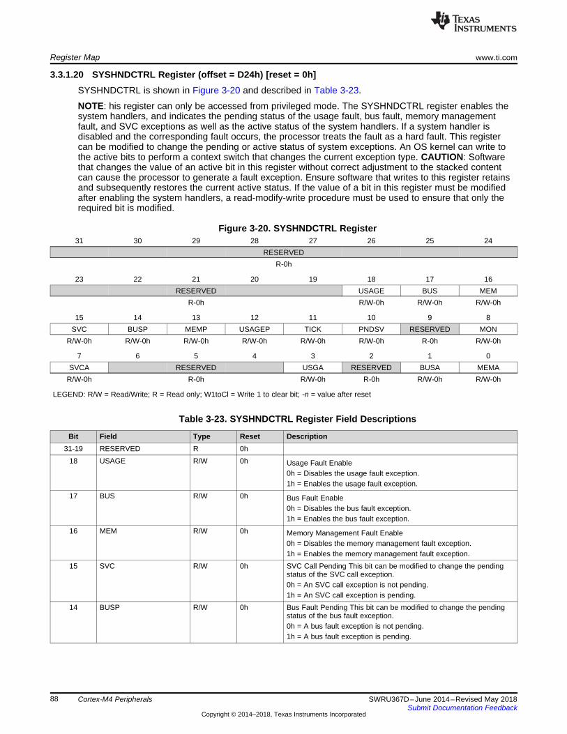
Register Map www.ti.com
88 SWRU367D–June 2014–Revised May 2018Submit Documentation Feedback
Copyright © 2014–2018, Texas Instruments Incorporated
Cortex-M4 Peripherals
3.3.1.20 SYSHNDCTRL Register (offset = D24h) [reset = 0h]SYSHNDCTRL is shown in Figure 3-20 and described in Table 3-23.
NOTE: his register can only be accessed from privileged mode. The SYSHNDCTRL register enables thesystem handlers, and indicates the pending status of the usage fault, bus fault, memory managementfault, and SVC exceptions as well as the active status of the system handlers. If a system handler isdisabled and the corresponding fault occurs, the processor treats the fault as a hard fault. This registercan be modified to change the pending or active status of system exceptions. An OS kernel can write tothe active bits to perform a context switch that changes the current exception type. CAUTION: Softwarethat changes the value of an active bit in this register without correct adjustment to the stacked contentcan cause the processor to generate a fault exception. Ensure software that writes to this register retainsand subsequently restores the current active status. If the value of a bit in this register must be modifiedafter enabling the system handlers, a read-modify-write procedure must be used to ensure that only therequired bit is modified.
Figure 3-20. SYSHNDCTRL Register31 30 29 28 27 26 25 24
RESERVEDR-0h
23 22 21 20 19 18 17 16RESERVED USAGE BUS MEM
R-0h R/W-0h R/W-0h R/W-0h
15 14 13 12 11 10 9 8SVC BUSP MEMP USAGEP TICK PNDSV RESERVED MON
R/W-0h R/W-0h R/W-0h R/W-0h R/W-0h R/W-0h R-0h R/W-0h
7 6 5 4 3 2 1 0SVCA RESERVED USGA RESERVED BUSA MEMA
R/W-0h R-0h R/W-0h R-0h R/W-0h R/W-0h
LEGEND: R/W = Read/Write; R = Read only; W1toCl = Write 1 to clear bit; -n = value after reset
Table 3-23. SYSHNDCTRL Register Field Descriptions
Bit Field Type Reset Description31-19 RESERVED R 0h
18 USAGE R/W 0h Usage Fault Enable0h = Disables the usage fault exception.1h = Enables the usage fault exception.
17 BUS R/W 0h Bus Fault Enable0h = Disables the bus fault exception.1h = Enables the bus fault exception.
16 MEM R/W 0h Memory Management Fault Enable0h = Disables the memory management fault exception.1h = Enables the memory management fault exception.
15 SVC R/W 0h SVC Call Pending This bit can be modified to change the pendingstatus of the SVC call exception.0h = An SVC call exception is not pending.1h = An SVC call exception is pending.
14 BUSP R/W 0h Bus Fault Pending This bit can be modified to change the pendingstatus of the bus fault exception.0h = A bus fault exception is not pending.1h = A bus fault exception is pending.
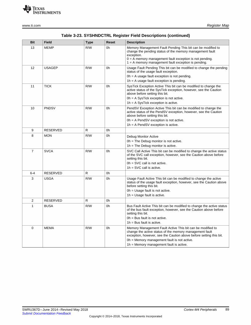
www.ti.com Register Map
89SWRU367D–June 2014–Revised May 2018Submit Documentation Feedback
Copyright © 2014–2018, Texas Instruments Incorporated
Cortex-M4 Peripherals
Table 3-23. SYSHNDCTRL Register Field Descriptions (continued)Bit Field Type Reset Description13 MEMP R/W 0h Memory Management Fault Pending This bit can be modified to
change the pending status of the memory management faultexception.0 = A memory management fault exception is not pending.1 = A memory management fault exception is pending.
12 USAGEP R/W 0h Usage Fault Pending This bit can be modified to change the pendingstatus of the usage fault exception.0h = A usage fault exception is not pending.1h = A usage fault exception is pending.
11 TICK R/W 0h SysTick Exception Active This bit can be modified to change theactive status of the SysTick exception, however, see the Cautionabove before setting this bit.0h = A SysTick exception is not active.1h = A SysTick exception is active.
10 PNDSV R/W 0h PendSV Exception Active This bit can be modified to change theactive status of the PendSV exception, however, see the Cautionabove before setting this bit.0h = A PendSV exception is not active.1h = A PendSV exception is active.
9 RESERVED R 0h8 MON R/W 0h Debug Monitor Active
0h = The Debug monitor is not active.1h = The Debug monitor is active.
7 SVCA R/W 0h SVC Call Active This bit can be modified to change the active statusof the SVC call exception, however, see the Caution above beforesetting this bit.0h = SVC call is not active.1h = SVC call is active.
6-4 RESERVED R 0h3 USGA R/W 0h Usage Fault Active This bit can be modified to change the active
status of the usage fault exception, however, see the Caution abovebefore setting this bit.0h = Usage fault is not active.1h = Usage fault is active.
2 RESERVED R 0h1 BUSA R/W 0h Bus Fault Active This bit can be modified to change the active status
of the bus fault exception, however, see the Caution above beforesetting this bit.0h = Bus fault is not active.1h = Bus fault is active.
0 MEMA R/W 0h Memory Management Fault Active This bit can be modified tochange the active status of the memory management faultexception, however, see the Caution above before setting this bit.0h = Memory management fault is not active.1h = Memory management fault is active.
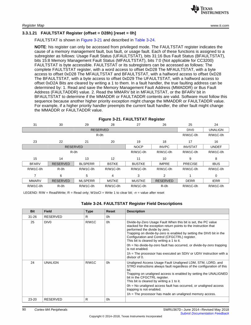
Register Map www.ti.com
90 SWRU367D–June 2014–Revised May 2018Submit Documentation Feedback
Copyright © 2014–2018, Texas Instruments Incorporated
Cortex-M4 Peripherals
3.3.1.21 FAULTSTAT Register (offset = D28h) [reset = 0h]FAULTSTAT is shown in Figure 3-21 and described in Table 3-24.
NOTE: his register can only be accessed from privileged mode. The FAULTSTAT register indicates thecause of a memory management fault, bus fault, or usage fault. Each of these functions is assigned to asubregister as follows: Usage Fault Status (UFAULTSTAT), bits 31:16 Bus Fault Status (BFAULTSTAT),bits 15:8 Memory Management Fault Status (MFAULTSTAT), bits 7:0 (Not applicable for CC3200)FAULTSTAT is byte accessible. FAULTSTAT or its subregisters can be accessed as follows: Thecomplete FAULTSTAT register, with a word access to offset 0xD28 The MFAULTSTAT, with a byteaccess to offset 0xD28 The MFAULTSTAT and BFAULTSTAT, with a halfword access to offset 0xD28The BFAULTSTAT, with a byte access to offset 0xD29 The UFAULTSTAT, with a halfword access tooffset 0xD2A Bits are cleared by writing a 1 to them. In a fault handler, the true faulting address can bedetermined by: 1. Read and save the Memory Management Fault Address (MMADDR) or Bus FaultAddress (FAULTADDR) value. 2. Read the MMARV bit in MFAULTSTAT, or the BFARV bit inBFAULTSTAT to determine if the MMADDR or FAULTADDR contents are valid. Software must follow thissequence because another higher priority exception might change the MMADDR or FAULTADDR value.For example, if a higher priority handler preempts the current fault handler, the other fault might changethe MMADDR or FAULTADDR value.
Figure 3-21. FAULTSTAT Register31 30 29 28 27 26 25 24
RESERVED DIV0 UNALIGNR-0h R/W1C-0h R/W1C-0h
23 22 21 20 19 18 17 16RESERVED NOCP INVPC INVSTAT UNDEF
R-0h R/W1C-0h R/W1C-0h R/W1C-0h R/W1C-0h
15 14 13 12 11 10 9 8BFARV RESERVED BLSPERR BSTKE BUSTKE IMPRE PRECISE IBUS
R/W1C-0h R-0h R/W1C-0h R/W1C-0h R/W1C-0h R/W1C-0h R/W1C-0h R/W1C-0h
7 6 5 4 3 2 1 0MMARV RESERVED MLSPERR MSTKE MUSTKE RESERVED DERR IERR
R/W1C-0h R-0h R/W1C-0h R/W1C-0h R/W1C-0h R-0h R/W1C-0h R/W1C-0h
LEGEND: R/W = Read/Write; R = Read only; W1toCl = Write 1 to clear bit; -n = value after reset
Table 3-24. FAULTSTAT Register Field Descriptions
Bit Field Type Reset Description31-26 RESERVED R 0h
25 DIV0 R/W1C 0h Divide-by-Zero Usage Fault When this bit is set, the PC valuestacked for the exception return points to the instruction thatperformed the divide by zero.Trapping on divide-by-zero is enabled by setting the DIV0 bit in theConfiguration and Control (CFGCTRL) register.This bit is cleared by writing a 1 to it.0h = No divide-by-zero fault has occurred, or divide-by-zero trappingis not enabled.1h = The processor has executed an SDIV or UDIV instruction with adivisor of 0.
24 UNALIGN R/W1C 0h Unaligned Access Usage Fault Unaligned LDM, STM, LDRD, andSTRD instructions always fault regardless of the configuration of thisbit.Trapping on unaligned access is enabled by setting the UNALIGNEDbit in the CFGCTRL register.This bit is cleared by writing a 1 to it.0h = No unaligned access fault has occurred, or unaligned accesstrapping is not enabled.1h = The processor has made an unaligned memory access.
23-20 RESERVED R 0h
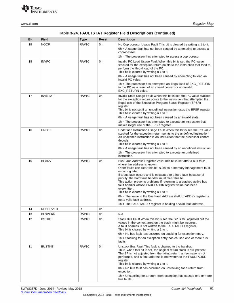
www.ti.com Register Map
91SWRU367D–June 2014–Revised May 2018Submit Documentation Feedback
Copyright © 2014–2018, Texas Instruments Incorporated
Cortex-M4 Peripherals
Table 3-24. FAULTSTAT Register Field Descriptions (continued)Bit Field Type Reset Description19 NOCP R/W1C 0h No Coprocessor Usage Fault This bit is cleared by writing a 1 to it.
0h = A usage fault has not been caused by attempting to access acoprocessor.1h = The processor has attempted to access a coprocessor.
18 INVPC R/W1C 0h Invalid PC Load Usage Fault When this bit is set, the PC valuestacked for the exception return points to the instruction that tried toperform the illegal load of the PC.This bit is cleared by writing a 1 to it.0h = A usage fault has not been caused by attempting to load aninvalid PC value.1h = The processor has attempted an illegal load of EXC_RETURNto the PC as a result of an invalid context or an invalidEXC_RETURN value.
17 INVSTAT R/W1C 0h Invalid State Usage Fault When this bit is set, the PC value stackedfor the exception return points to the instruction that attempted theillegal use of the Execution Program Status Register (EPSR)register.This bit is not set if an undefined instruction uses the EPSR register.This bit is cleared by writing a 1 to it.0h = A usage fault has not been caused by an invalid state.1h = The processor has attempted to execute an instruction thatmakes illegal use of the EPSR register.
16 UNDEF R/W1C 0h Undefined Instruction Usage Fault When this bit is set, the PC valuestacked for the exception return points to the undefined instruction.An undefined instruction is an instruction that the processor cannotdecode.This bit is cleared by writing a 1 to it.0h = A usage fault has not been caused by an undefined instruction.1h = The processor has attempted to execute an undefinedinstruction.
15 BFARV R/W1C 0h Bus Fault Address Register Valid This bit is set after a bus fault,where the address is known.Other faults can clear this bit, such as a memory management faultoccurring later.If a bus fault occurs and is escalated to a hard fault because ofpriority, the hard fault handler must clear this bit.This action prevents problems if returning to a stacked active busfault handler whose FAULTADDR register value has beenoverwritten.This bit is cleared by writing a 1 to it.0h = The value in the Bus Fault Address (FAULTADDR) register isnot a valid fault address.1h = The FAULTADDR register is holding a valid fault address.
14 RESERVED R 0h13 BLSPERR R/W1C 0h N/A12 BSTKE R/W1C 0h Stack Bus Fault When this bit is set, the SP is still adjusted but the
values in the context area on the stack might be incorrect.A fault address is not written to the FAULTADDR register.This bit is cleared by writing a 1 to it.0h = No bus fault has occurred on stacking for exception entry.1h = Stacking for an exception entry has caused one or more busfaults.
11 BUSTKE R/W1C 0h Unstack Bus Fault This fault is chained to the handler.Thus, when this bit is set, the original return stack is still present.The SP is not adjusted from the failing return, a new save is notperformed, and a fault address is not written to the FAULTADDRregister.This bit is cleared by writing a 1 to it.0h = No bus fault has occurred on unstacking for a return fromexception.1h = Unstacking for a return from exception has caused one or morebus faults.
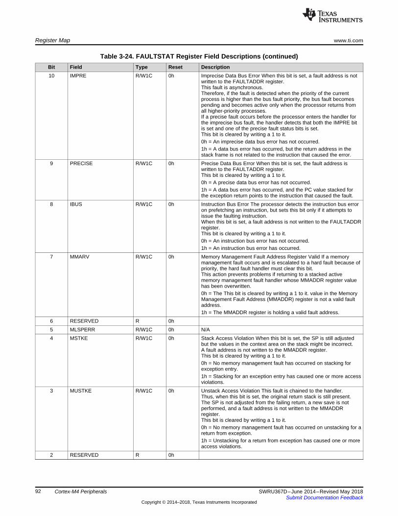
Register Map www.ti.com
92 SWRU367D–June 2014–Revised May 2018Submit Documentation Feedback
Copyright © 2014–2018, Texas Instruments Incorporated
Cortex-M4 Peripherals
Table 3-24. FAULTSTAT Register Field Descriptions (continued)Bit Field Type Reset Description10 IMPRE R/W1C 0h Imprecise Data Bus Error When this bit is set, a fault address is not
written to the FAULTADDR register.This fault is asynchronous.Therefore, if the fault is detected when the priority of the currentprocess is higher than the bus fault priority, the bus fault becomespending and becomes active only when the processor returns fromall higher-priority processes.If a precise fault occurs before the processor enters the handler forthe imprecise bus fault, the handler detects that both the IMPRE bitis set and one of the precise fault status bits is set.This bit is cleared by writing a 1 to it.0h = An imprecise data bus error has not occurred.1h = A data bus error has occurred, but the return address in thestack frame is not related to the instruction that caused the error.
9 PRECISE R/W1C 0h Precise Data Bus Error When this bit is set, the fault address iswritten to the FAULTADDR register.This bit is cleared by writing a 1 to it.0h = A precise data bus error has not occurred.1h = A data bus error has occurred, and the PC value stacked forthe exception return points to the instruction that caused the fault.
8 IBUS R/W1C 0h Instruction Bus Error The processor detects the instruction bus erroron prefetching an instruction, but sets this bit only if it attempts toissue the faulting instruction.When this bit is set, a fault address is not written to the FAULTADDRregister.This bit is cleared by writing a 1 to it.0h = An instruction bus error has not occurred.1h = An instruction bus error has occurred.
7 MMARV R/W1C 0h Memory Management Fault Address Register Valid If a memorymanagement fault occurs and is escalated to a hard fault because ofpriority, the hard fault handler must clear this bit.This action prevents problems if returning to a stacked activememory management fault handler whose MMADDR register valuehas been overwritten.0h = The This bit is cleared by writing a 1 to it. value in the MemoryManagement Fault Address (MMADDR) register is not a valid faultaddress.1h = The MMADDR register is holding a valid fault address.
6 RESERVED R 0h5 MLSPERR R/W1C 0h N/A4 MSTKE R/W1C 0h Stack Access Violation When this bit is set, the SP is still adjusted
but the values in the context area on the stack might be incorrect.A fault address is not written to the MMADDR register.This bit is cleared by writing a 1 to it.0h = No memory management fault has occurred on stacking forexception entry.1h = Stacking for an exception entry has caused one or more accessviolations.
3 MUSTKE R/W1C 0h Unstack Access Violation This fault is chained to the handler.Thus, when this bit is set, the original return stack is still present.The SP is not adjusted from the failing return, a new save is notperformed, and a fault address is not written to the MMADDRregister.This bit is cleared by writing a 1 to it.0h = No memory management fault has occurred on unstacking for areturn from exception.1h = Unstacking for a return from exception has caused one or moreaccess violations.
2 RESERVED R 0h
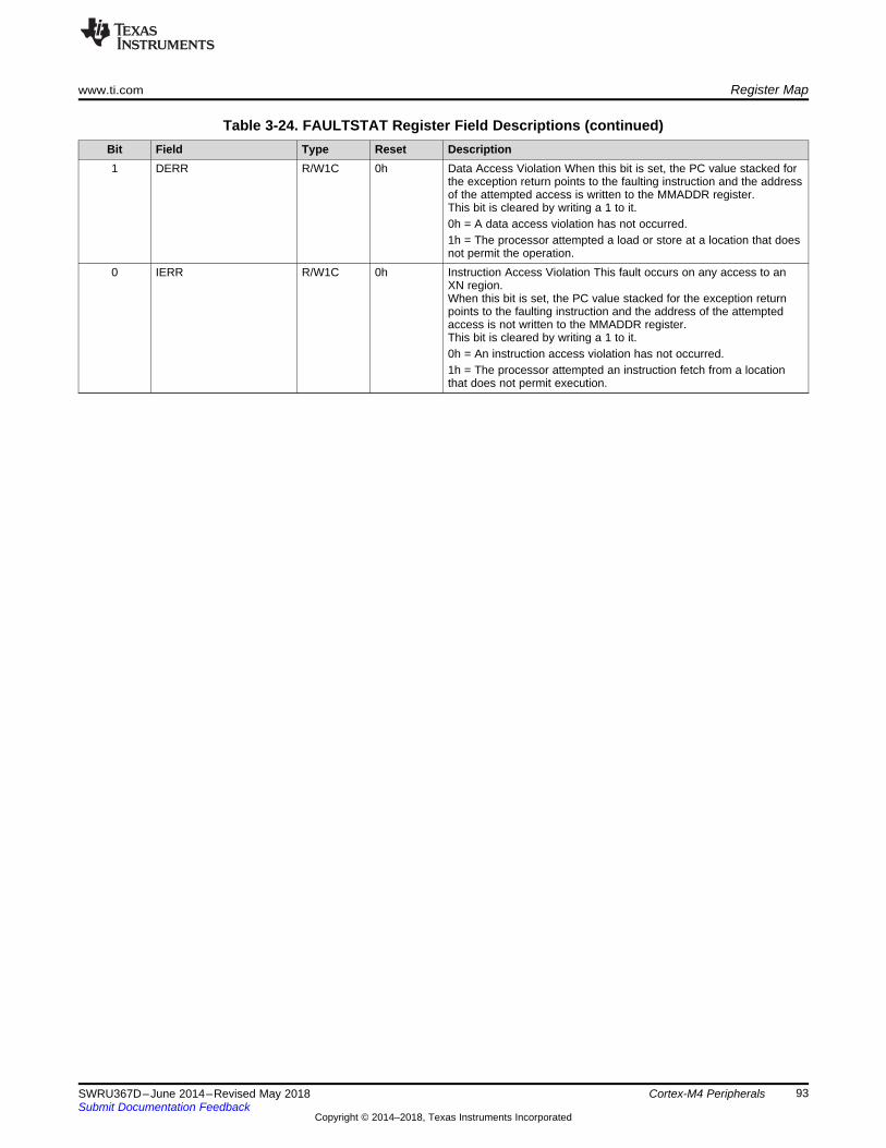
www.ti.com Register Map
93SWRU367D–June 2014–Revised May 2018Submit Documentation Feedback
Copyright © 2014–2018, Texas Instruments Incorporated
Cortex-M4 Peripherals
Table 3-24. FAULTSTAT Register Field Descriptions (continued)Bit Field Type Reset Description1 DERR R/W1C 0h Data Access Violation When this bit is set, the PC value stacked for
the exception return points to the faulting instruction and the addressof the attempted access is written to the MMADDR register.This bit is cleared by writing a 1 to it.0h = A data access violation has not occurred.1h = The processor attempted a load or store at a location that doesnot permit the operation.
0 IERR R/W1C 0h Instruction Access Violation This fault occurs on any access to anXN region.When this bit is set, the PC value stacked for the exception returnpoints to the faulting instruction and the address of the attemptedaccess is not written to the MMADDR register.This bit is cleared by writing a 1 to it.0h = An instruction access violation has not occurred.1h = The processor attempted an instruction fetch from a locationthat does not permit execution.
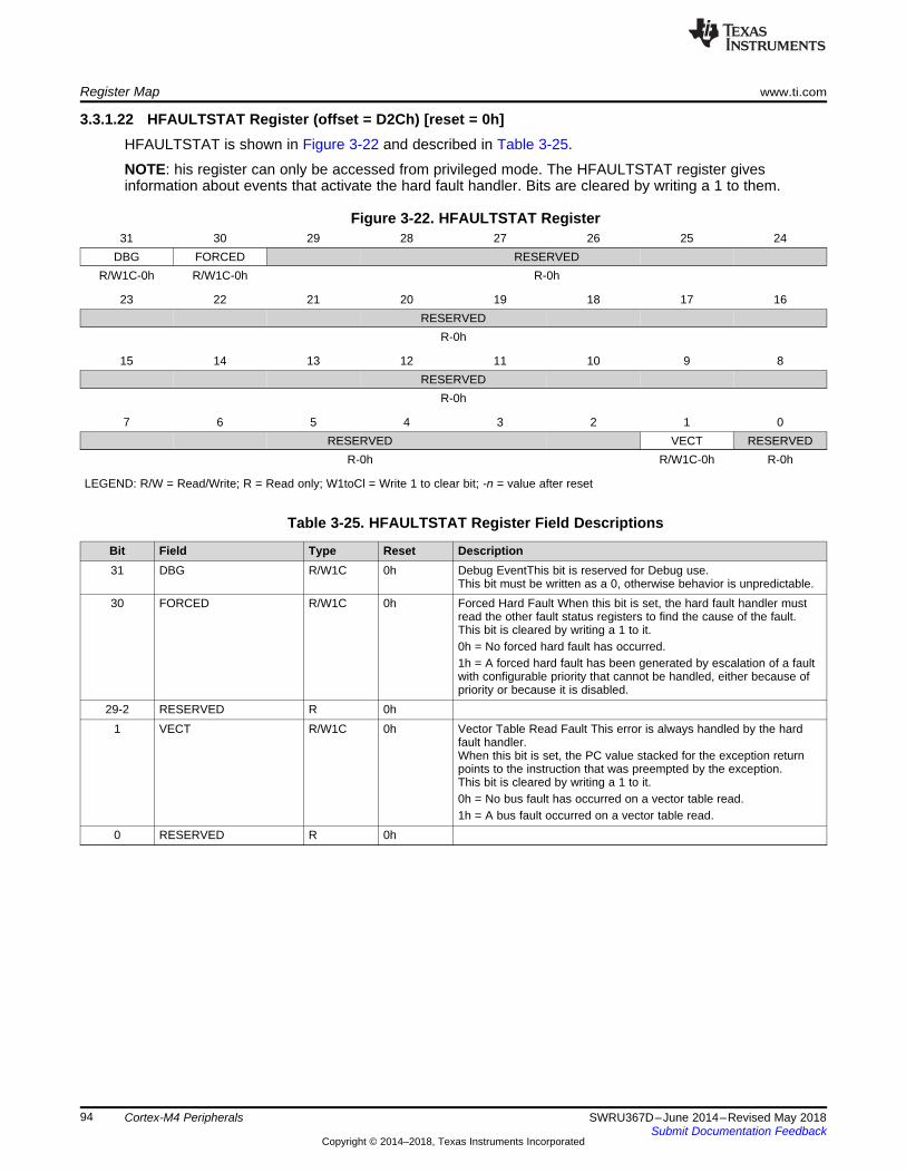
Register Map www.ti.com
94 SWRU367D–June 2014–Revised May 2018Submit Documentation Feedback
Copyright © 2014–2018, Texas Instruments Incorporated
Cortex-M4 Peripherals
3.3.1.22 HFAULTSTAT Register (offset = D2Ch) [reset = 0h]HFAULTSTAT is shown in Figure 3-22 and described in Table 3-25.
NOTE: his register can only be accessed from privileged mode. The HFAULTSTAT register givesinformation about events that activate the hard fault handler. Bits are cleared by writing a 1 to them.
Figure 3-22. HFAULTSTAT Register31 30 29 28 27 26 25 24
DBG FORCED RESERVEDR/W1C-0h R/W1C-0h R-0h
23 22 21 20 19 18 17 16RESERVED
R-0h
15 14 13 12 11 10 9 8RESERVED
R-0h
7 6 5 4 3 2 1 0RESERVED VECT RESERVED
R-0h R/W1C-0h R-0h
LEGEND: R/W = Read/Write; R = Read only; W1toCl = Write 1 to clear bit; -n = value after reset
Table 3-25. HFAULTSTAT Register Field Descriptions
Bit Field Type Reset Description31 DBG R/W1C 0h Debug EventThis bit is reserved for Debug use.
This bit must be written as a 0, otherwise behavior is unpredictable.30 FORCED R/W1C 0h Forced Hard Fault When this bit is set, the hard fault handler must
read the other fault status registers to find the cause of the fault.This bit is cleared by writing a 1 to it.0h = No forced hard fault has occurred.1h = A forced hard fault has been generated by escalation of a faultwith configurable priority that cannot be handled, either because ofpriority or because it is disabled.
29-2 RESERVED R 0h1 VECT R/W1C 0h Vector Table Read Fault This error is always handled by the hard
fault handler.When this bit is set, the PC value stacked for the exception returnpoints to the instruction that was preempted by the exception.This bit is cleared by writing a 1 to it.0h = No bus fault has occurred on a vector table read.1h = A bus fault occurred on a vector table read.
0 RESERVED R 0h
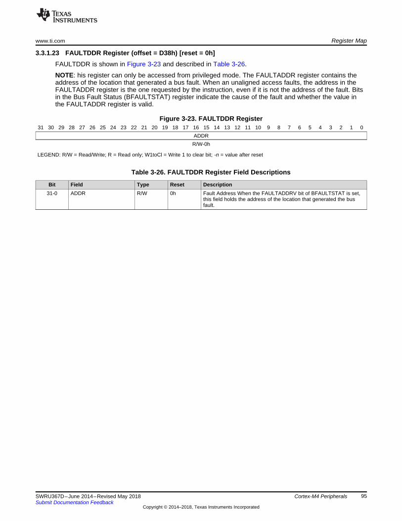
www.ti.com Register Map
95SWRU367D–June 2014–Revised May 2018Submit Documentation Feedback
Copyright © 2014–2018, Texas Instruments Incorporated
Cortex-M4 Peripherals
3.3.1.23 FAULTDDR Register (offset = D38h) [reset = 0h]FAULTDDR is shown in Figure 3-23 and described in Table 3-26.
NOTE: his register can only be accessed from privileged mode. The FAULTADDR register contains theaddress of the location that generated a bus fault. When an unaligned access faults, the address in theFAULTADDR register is the one requested by the instruction, even if it is not the address of the fault. Bitsin the Bus Fault Status (BFAULTSTAT) register indicate the cause of the fault and whether the value inthe FAULTADDR register is valid.
Figure 3-23. FAULTDDR Register31 30 29 28 27 26 25 24 23 22 21 20 19 18 17 16 15 14 13 12 11 10 9 8 7 6 5 4 3 2 1 0
ADDRR/W-0h
LEGEND: R/W = Read/Write; R = Read only; W1toCl = Write 1 to clear bit; -n = value after reset
Table 3-26. FAULTDDR Register Field Descriptions
Bit Field Type Reset Description31-0 ADDR R/W 0h Fault Address When the FAULTADDRV bit of BFAULTSTAT is set,
this field holds the address of the location that generated the busfault.
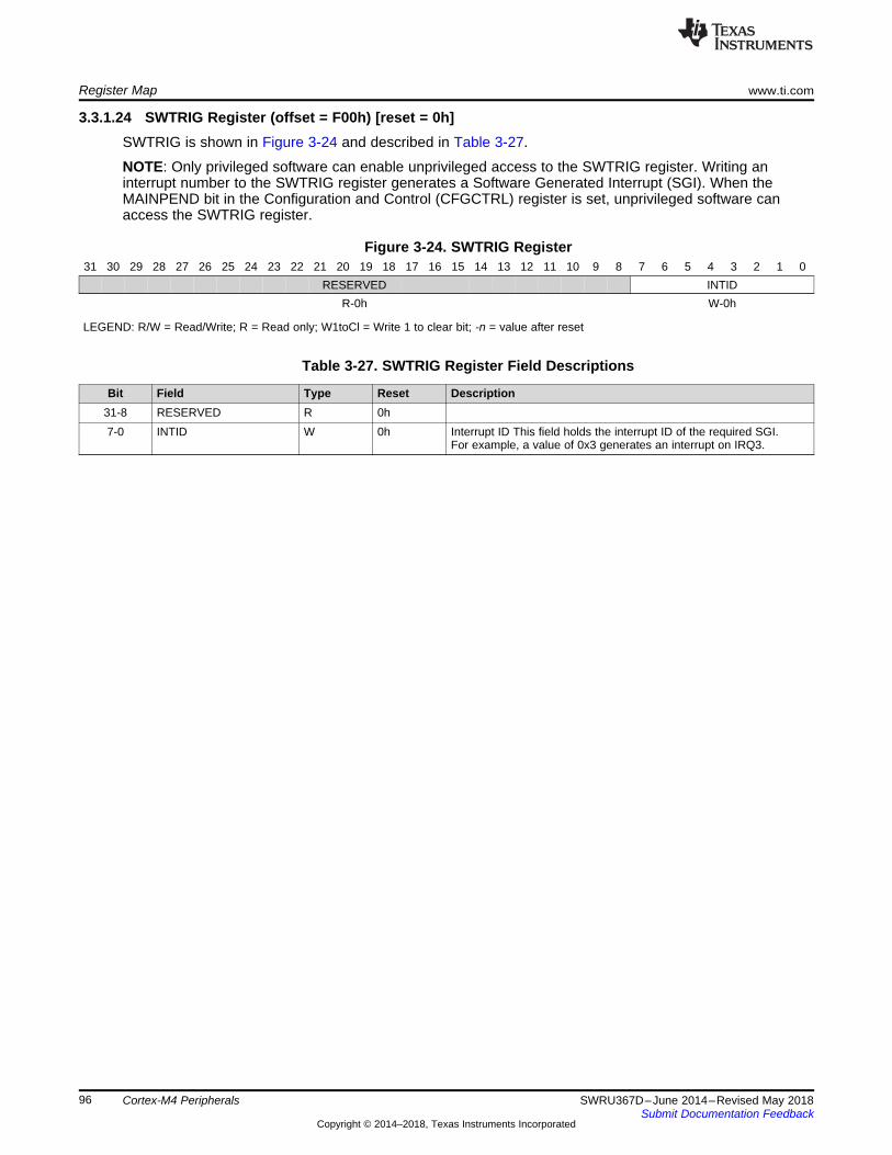
Register Map www.ti.com
96 SWRU367D–June 2014–Revised May 2018Submit Documentation Feedback
Copyright © 2014–2018, Texas Instruments Incorporated
Cortex-M4 Peripherals
3.3.1.24 SWTRIG Register (offset = F00h) [reset = 0h]SWTRIG is shown in Figure 3-24 and described in Table 3-27.
NOTE: Only privileged software can enable unprivileged access to the SWTRIG register. Writing aninterrupt number to the SWTRIG register generates a Software Generated Interrupt (SGI). When theMAINPEND bit in the Configuration and Control (CFGCTRL) register is set, unprivileged software canaccess the SWTRIG register.
Figure 3-24. SWTRIG Register31 30 29 28 27 26 25 24 23 22 21 20 19 18 17 16 15 14 13 12 11 10 9 8 7 6 5 4 3 2 1 0
RESERVED INTIDR-0h W-0h
LEGEND: R/W = Read/Write; R = Read only; W1toCl = Write 1 to clear bit; -n = value after reset
Table 3-27. SWTRIG Register Field Descriptions
Bit Field Type Reset Description31-8 RESERVED R 0h7-0 INTID W 0h Interrupt ID This field holds the interrupt ID of the required SGI.
For example, a value of 0x3 generates an interrupt on IRQ3.
97SWRU367D–June 2014–Revised May 2018Submit Documentation Feedback
Copyright © 2014–2018, Texas Instruments Incorporated
Direct Memory Access (DMA)
Chapter 4SWRU367D–June 2014–Revised May 2018
Direct Memory Access (DMA)
Topic ........................................................................................................................... Page
4.1 Overview ........................................................................................................... 984.2 Functional Description........................................................................................ 984.3 Register Description ......................................................................................... 108
Overview www.ti.com
98 SWRU367D–June 2014–Revised May 2018Submit Documentation Feedback
Copyright © 2014–2018, Texas Instruments Incorporated
Direct Memory Access (DMA)
4.1 OverviewThe CC3200 microcontroller includes a Direct Memory Access (DMA) controller, known as micro-DMA(μDMA). The μDMA controller provides a way to offload data transfer tasks from the Cortex-M4 processor,allowing for more efficient use of the processor and the available bus bandwidth. The μDMA controller canperform transfers between memory and peripherals. It has dedicated channels for each supported on-chipmodule and can be programmed to automatically perform transfers between peripherals and memory, asthe peripheral is ready to transfer more data.
The μDMA controller provides the following features:• 32-channel configurable µDMA controller• Support for memory-to-memory, memory-to-peripheral, and peripheral-to-memory in multiple transfer
modes– Basic for simple transfer scenarios– Ping-pong for continuous data flow– Scatter-gather for a programmable list of up to 256 arbitrary transfers initiated from a single request
• Highly flexible and configurable channel operation– Independently configured and operated channels– Dedicated channels for supported on-chip modules– One channel each for receive and transmit path for bidirectional modules– Dedicated channel for software-initiated transfers– Optional software-initiated requests for any channel
• Two levels of priority• Design optimizations for improved bus access performance between µDMA controller and the
processor core– µDMA controller access is subordinate to core access
• Data sizes of 8, 16, and 32 bits• Transfer size is programmable in binary steps from 1 to 1024• Source and destination address increment size of byte, half-word, word, or no increment• Interrupt on transfer completion, with a separate interrupt per channel
4.2 Functional DescriptionThe μDMA controller is a flexible and highly configurable DMA controller designed to work efficiently withthe Cortex-M4 processor core. It supports multiple data sizes and address increment schemes, multiplelevels of priority among DMA channels, and several transfer modes to allow for sophisticated programmeddata transfers. The μDMA controller's usage of the bus is always subordinate to the processor core, so itnever delays a bus transaction by the processor.
Because the μDMA controller is only using otherwise-idle bus cycles, the data transfer bandwidth itprovides is essentially free, with no impact on the rest of the system. The bus architecture has beenoptimized to greatly enhance the ability of the processor core and the μDMA controller to efficiently sharethe on-chip bus, thus improving performance. The optimizations include peripheral bus segmentation,which in many cases allow both the processor core and the μDMA controller to access the bus andperform simultaneous data transfers.
Each supported peripheral function has a dedicated channel on the μDMA controller that can beconfigured independently. The μDMA controller implements a configuration method using channel controlstructures maintained in system memory by the processor. While simple transfer modes are supported, itis also possible to build up sophisticated task lists in memory that allow the μDMA controller to performarbitrary-sized transfers to and from arbitrary locations as part of a single transfer request. The μDMAcontroller also supports the use of ping-pong buffering to accommodate constant streaming of data to orfrom a peripheral.
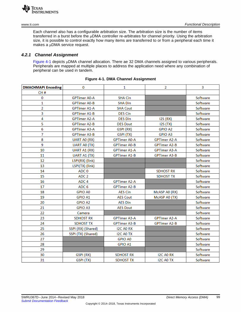
www.ti.com Functional Description
99SWRU367D–June 2014–Revised May 2018Submit Documentation Feedback
Copyright © 2014–2018, Texas Instruments Incorporated
Direct Memory Access (DMA)
Each channel also has a configurable arbitration size. The arbitration size is the number of itemstransferred in a burst before the μDMA controller re-arbitrates for channel priority. Using the arbitrationsize, it is possible to control exactly how many items are transferred to or from a peripheral each time itmakes a μDMA service request.
4.2.1 Channel AssignmentFigure 4-1 depicts μDMA channel allocation. There ae 32 DMA channels assigned to various peripherals.Peripherals are mapped at multiple places to address the application need where any combination ofperipheral can be used in tandem.
Figure 4-1. DMA Channel Assignment
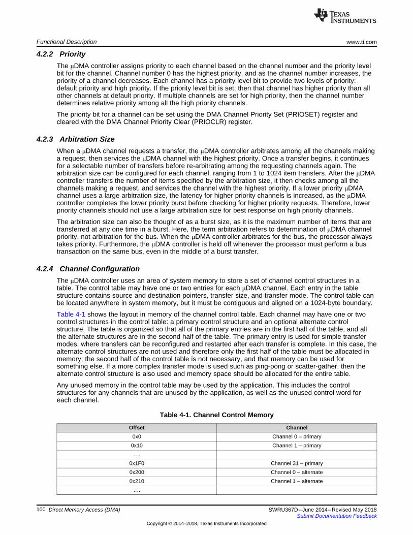
Functional Description www.ti.com
100 SWRU367D–June 2014–Revised May 2018Submit Documentation Feedback
Copyright © 2014–2018, Texas Instruments Incorporated
Direct Memory Access (DMA)
4.2.2 PriorityThe μDMA controller assigns priority to each channel based on the channel number and the priority levelbit for the channel. Channel number 0 has the highest priority, and as the channel number increases, thepriority of a channel decreases. Each channel has a priority level bit to provide two levels of priority:default priority and high priority. If the priority level bit is set, then that channel has higher priority than allother channels at default priority. If multiple channels are set for high priority, then the channel numberdetermines relative priority among all the high priority channels.
The priority bit for a channel can be set using the DMA Channel Priority Set (PRIOSET) register andcleared with the DMA Channel Priority Clear (PRIOCLR) register.
4.2.3 Arbitration SizeWhen a μDMA channel requests a transfer, the μDMA controller arbitrates among all the channels makinga request, then services the μDMA channel with the highest priority. Once a transfer begins, it continuesfor a selectable number of transfers before re-arbitrating among the requesting channels again. Thearbitration size can be configured for each channel, ranging from 1 to 1024 item transfers. After the μDMAcontroller transfers the number of items specified by the arbitration size, it then checks among all thechannels making a request, and services the channel with the highest priority. If a lower priority μDMAchannel uses a large arbitration size, the latency for higher priority channels is increased, as the μDMAcontroller completes the lower priority burst before checking for higher priority requests. Therefore, lowerpriority channels should not use a large arbitration size for best response on high priority channels.
The arbitration size can also be thought of as a burst size, as it is the maximum number of items that aretransferred at any one time in a burst. Here, the term arbitration refers to determination of μDMA channelpriority, not arbitration for the bus. When the μDMA controller arbitrates for the bus, the processor alwaystakes priority. Furthermore, the μDMA controller is held off whenever the processor must perform a bustransaction on the same bus, even in the middle of a burst transfer.
4.2.4 Channel ConfigurationThe μDMA controller uses an area of system memory to store a set of channel control structures in atable. The control table may have one or two entries for each μDMA channel. Each entry in the tablestructure contains source and destination pointers, transfer size, and transfer mode. The control table canbe located anywhere in system memory, but it must be contiguous and aligned on a 1024-byte boundary.
Table 4-1 shows the layout in memory of the channel control table. Each channel may have one or twocontrol structures in the control table: a primary control structure and an optional alternate controlstructure. The table is organized so that all of the primary entries are in the first half of the table, and allthe alternate structures are in the second half of the table. The primary entry is used for simple transfermodes, where transfers can be reconfigured and restarted after each transfer is complete. In this case, thealternate control structures are not used and therefore only the first half of the table must be allocated inmemory; the second half of the control table is not necessary, and that memory can be used forsomething else. If a more complex transfer mode is used such as ping-pong or scatter-gather, then thealternate control structure is also used and memory space should be allocated for the entire table.
Any unused memory in the control table may be used by the application. This includes the controlstructures for any channels that are unused by the application, as well as the unused control word foreach channel.
Table 4-1. Channel Control Memory
Offset Channel0x0 Channel 0 – primary0x10 Channel 1 – primary….
0x1F0 Channel 31 – primary0x200 Channel 0 – alternate0x210 Channel 1 – alternate
….
www.ti.com Functional Description
101SWRU367D–June 2014–Revised May 2018Submit Documentation Feedback
Copyright © 2014–2018, Texas Instruments Incorporated
Direct Memory Access (DMA)
Table 4-1. Channel Control Memory (continued)Offset Channel0x3F0 Channel 31 – alternate
Table 4-2 shows an individual control structure entry in the control table. Each entry is aligned on a 16-byte boundary. The entry contains four long words: the source end pointer, the destination end pointer, thecontrol word, and an unused entry. The end pointers point to the ending address of the transfer and areinclusive. If the source or destination is non-incrementing (as for a peripheral register), the pointer shouldpoint to the transfer address.
Table 4-2. Individual Control Structure
Offset Description0x000 Source end pointer0x004 Destination end pointer0x008 Control word0x00C Reserved
Transfer size is part of the control word. At the end of a transfer, the transfer size indicates 0, and thetransfer mode indicates "stopped." Because the control word is modified by the μDMA controller, it mustbe reconfigured before each new transfer. The source and destination end pointers are not modified, sothey can be left unchanged if the source or destination addresses remain the same.
Prior to starting a transfer, a μDMA channel must be enabled by setting the appropriate bit in the DMAChannel Enable Set (ENASET) register. A channel can be disabled by setting the channel bit in the DMAChannel Enable Clear (ENACLR) register. At the end of a complete μDMA transfer, the controllerautomatically disables the channel.
4.2.5 Transfer ModeThe μDMA controller supports several transfer modes. Two of the modes support simple one-timetransfers. Several complex modes support a continuous flow of data.
4.2.5.1 Stop ModeWhile stop is not actually a transfer mode, it is a valid value for the mode field of the control word. Whenthe mode field has this value, the μDMA controller does not perform any transfers, and disables thechannel if it is enabled.
4.2.5.2 Basic ModeIn basic mode, the μDMA controller performs transfers as long as there are more items to transfer, and atransfer request is present. This mode is used with peripherals that assert a μDMA request signalwhenever the peripheral is ready for a data transfer. Basic mode should not be used in any situationwhere the request is momentary, even though the entire transfer should be completed. For example, asoftware-initiated transfer creates a momentary request, and in basic mode, only the number of transfersspecified by the ARBSIZE field in the DMA Channel Control Word register are transferred on a softwarerequest, even if there is more data to transfer. When all of the items have been transferred using basicmode, the μDMA controller sets the channel to stop mode.
4.2.5.3 Auto ModeAuto mode is similar to basic mode, except that once a transfer request is received, the transfer runs tocompletion, even if the μDMA request is removed. This mode is suitable for software-triggered transfers.Generally, auto mode is not used with a peripheral. When all the items have been transferred using automode, the μDMA controller sets the mode for that channel to stop.
Functional Description www.ti.com
102 SWRU367D–June 2014–Revised May 2018Submit Documentation Feedback
Copyright © 2014–2018, Texas Instruments Incorporated
Direct Memory Access (DMA)
4.2.5.4 Ping-Pong ModePing-pong mode supports a continuous data flow to or from a peripheral. To use ping-pong mode, boththe primary and alternate data structures must be implemented. Both structures are set up by theprocessor for data transfer between memory and a peripheral. The transfer is started using the primarycontrol structure. When the transfer using the primary control structure is complete, the μDMA controllerreads the alternate control structure for that channel to continue the transfer. Each time this happens, aninterrupt is generated, and the processor can reload the control structure for the just-completed transfer.Data flow can continue indefinitely this way, using the primary and alternate control structures to switchback and forth between buffers as the data flows to or from the peripheral.
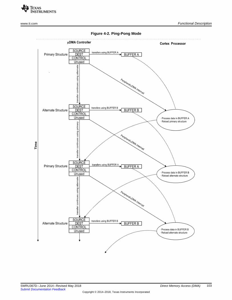
www.ti.com Functional Description
103SWRU367D–June 2014–Revised May 2018Submit Documentation Feedback
Copyright © 2014–2018, Texas Instruments Incorporated
Direct Memory Access (DMA)
Figure 4-2. Ping-Pong Mode
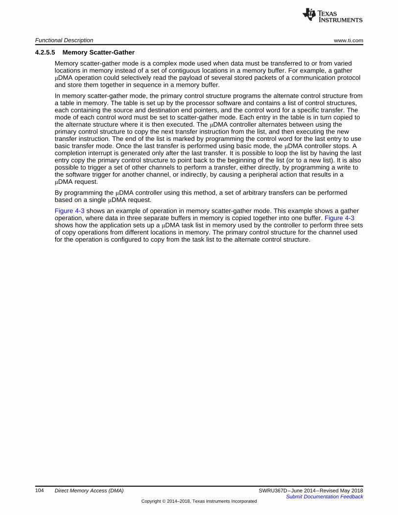
Functional Description www.ti.com
104 SWRU367D–June 2014–Revised May 2018Submit Documentation Feedback
Copyright © 2014–2018, Texas Instruments Incorporated
Direct Memory Access (DMA)
4.2.5.5 Memory Scatter-GatherMemory scatter-gather mode is a complex mode used when data must be transferred to or from variedlocations in memory instead of a set of contiguous locations in a memory buffer. For example, a gatherμDMA operation could selectively read the payload of several stored packets of a communication protocoland store them together in sequence in a memory buffer.
In memory scatter-gather mode, the primary control structure programs the alternate control structure froma table in memory. The table is set up by the processor software and contains a list of control structures,each containing the source and destination end pointers, and the control word for a specific transfer. Themode of each control word must be set to scatter-gather mode. Each entry in the table is in turn copied tothe alternate structure where it is then executed. The μDMA controller alternates between using theprimary control structure to copy the next transfer instruction from the list, and then executing the newtransfer instruction. The end of the list is marked by programming the control word for the last entry to usebasic transfer mode. Once the last transfer is performed using basic mode, the μDMA controller stops. Acompletion interrupt is generated only after the last transfer. It is possible to loop the list by having the lastentry copy the primary control structure to point back to the beginning of the list (or to a new list). It is alsopossible to trigger a set of other channels to perform a transfer, either directly, by programming a write tothe software trigger for another channel, or indirectly, by causing a peripheral action that results in aμDMA request.
By programming the μDMA controller using this method, a set of arbitrary transfers can be performedbased on a single μDMA request.
Figure 4-3 shows an example of operation in memory scatter-gather mode. This example shows a gatheroperation, where data in three separate buffers in memory is copied together into one buffer. Figure 4-3shows how the application sets up a μDMA task list in memory used by the controller to perform three setsof copy operations from different locations in memory. The primary control structure for the channel usedfor the operation is configured to copy from the task list to the alternate control structure.
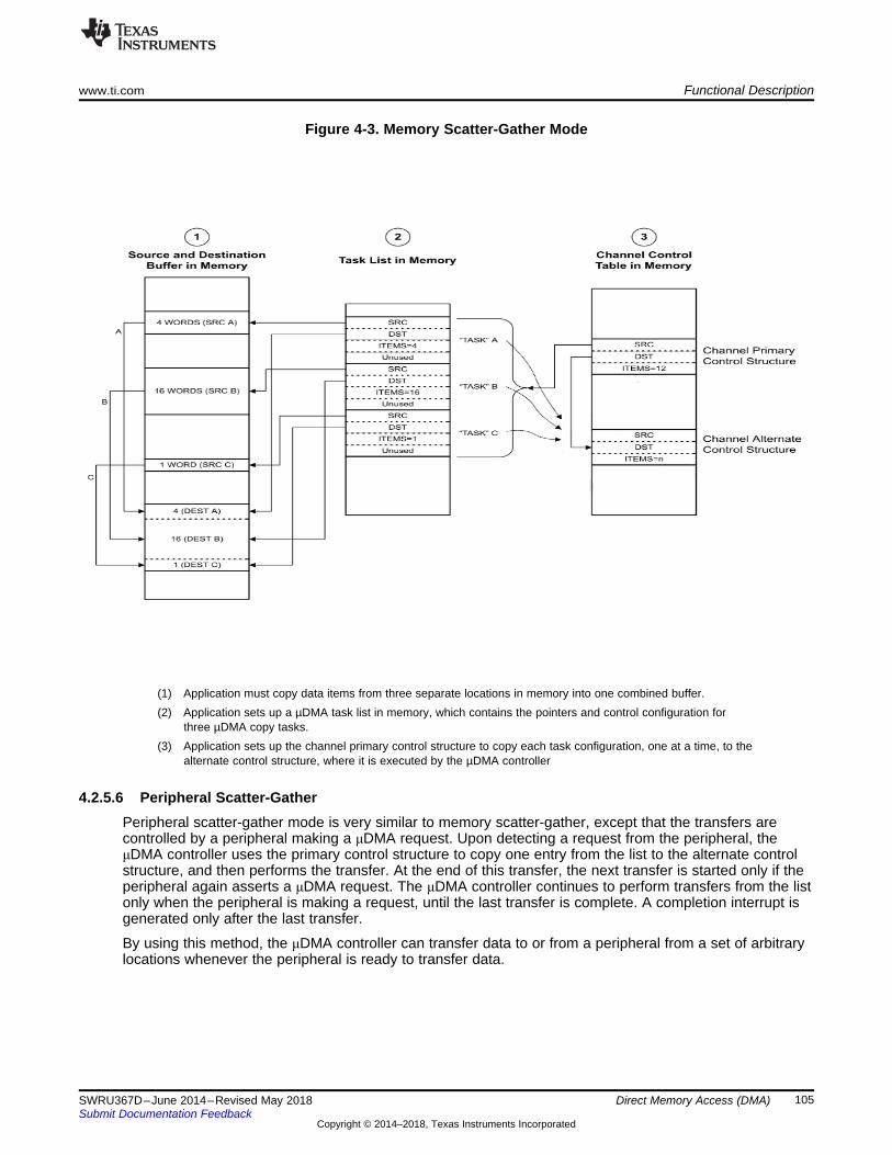
www.ti.com Functional Description
105SWRU367D–June 2014–Revised May 2018Submit Documentation Feedback
Copyright © 2014–2018, Texas Instruments Incorporated
Direct Memory Access (DMA)
Figure 4-3. Memory Scatter-Gather Mode
(1) Application must copy data items from three separate locations in memory into one combined buffer.(2) Application sets up a µDMA task list in memory, which contains the pointers and control configuration for
three µDMA copy tasks.(3) Application sets up the channel primary control structure to copy each task configuration, one at a time, to the
alternate control structure, where it is executed by the µDMA controller
4.2.5.6 Peripheral Scatter-GatherPeripheral scatter-gather mode is very similar to memory scatter-gather, except that the transfers arecontrolled by a peripheral making a μDMA request. Upon detecting a request from the peripheral, theμDMA controller uses the primary control structure to copy one entry from the list to the alternate controlstructure, and then performs the transfer. At the end of this transfer, the next transfer is started only if theperipheral again asserts a μDMA request. The μDMA controller continues to perform transfers from the listonly when the peripheral is making a request, until the last transfer is complete. A completion interrupt isgenerated only after the last transfer.
By using this method, the μDMA controller can transfer data to or from a peripheral from a set of arbitrarylocations whenever the peripheral is ready to transfer data.
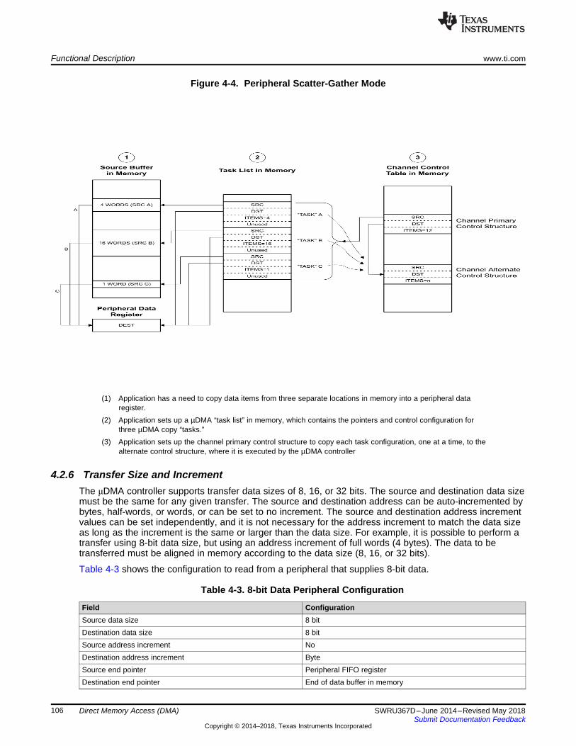
Functional Description www.ti.com
106 SWRU367D–June 2014–Revised May 2018Submit Documentation Feedback
Copyright © 2014–2018, Texas Instruments Incorporated
Direct Memory Access (DMA)
Figure 4-4. Peripheral Scatter-Gather Mode
(1) Application has a need to copy data items from three separate locations in memory into a peripheral dataregister.
(2) Application sets up a µDMA “task list” in memory, which contains the pointers and control configuration forthree µDMA copy “tasks.”
(3) Application sets up the channel primary control structure to copy each task configuration, one at a time, to thealternate control structure, where it is executed by the µDMA controller
4.2.6 Transfer Size and IncrementThe μDMA controller supports transfer data sizes of 8, 16, or 32 bits. The source and destination data sizemust be the same for any given transfer. The source and destination address can be auto-incremented bybytes, half-words, or words, or can be set to no increment. The source and destination address incrementvalues can be set independently, and it is not necessary for the address increment to match the data sizeas long as the increment is the same or larger than the data size. For example, it is possible to perform atransfer using 8-bit data size, but using an address increment of full words (4 bytes). The data to betransferred must be aligned in memory according to the data size (8, 16, or 32 bits).
Table 4-3 shows the configuration to read from a peripheral that supplies 8-bit data.
Table 4-3. 8-bit Data Peripheral Configuration
Field ConfigurationSource data size 8 bitDestination data size 8 bitSource address increment NoDestination address increment ByteSource end pointer Peripheral FIFO registerDestination end pointer End of data buffer in memory
www.ti.com Functional Description
107SWRU367D–June 2014–Revised May 2018Submit Documentation Feedback
Copyright © 2014–2018, Texas Instruments Incorporated
Direct Memory Access (DMA)
4.2.7 Peripheral InterfaceThere are two main classes of µDMA-connected peripherals:• Peripherals with FIFOs serviced by the µDMA to transmit or receive data• Peripherals that provide trigger inputs to the µDMA
4.2.7.1 FIFO PeripheralsFIFO peripherals contain a FIFO of data to be sent and a FIFO of data that has been received. The µDMAcontroller transfers data between these FIFOs and system memory. For example, when a UART FIFOcontains one or more entries, a single transfer request is sent to the µDMA for processing. If this requesthas not been processed and the UART FIFO reaches the interrupt FIFO level, another interrupt is sent tothe µDMA which is higher priority than the single-transfer request. In this instance, an ARBSIZ transfer isperformed as configured in the DMACHCTL register. After the transfer is complete, the µDMA sends areceive or transmit complete interrupt to the UART register.
If the SETn bit of the FIFO peripheral is set in the DMA Channel Useburst Set (DMAUSEBURSTSET)register, then the µDMA only performs transfers defined by the ARBSIZ bit field in the DMACHCTLregister for better bus utilization. For peripherals that tend to transmit and receive in bursts, such as theUART, TI recommends against the use of this configuration because it could cause the tail end oftransmissions to stick in the FIFO.
4.2.7.2 Trigger PeripheralsCertain peripherals, such as the general purpose timer, trigger an interrupt to the µDMA controller when aprogrammed event occurs. When a trigger event occurs, the µDMA executes a transfer defined by theARBSIZ bit field in the DMACHCTL register. If only a single transfer is needed for a µDMA trigger, thenthe ARBSIZ field is set to 0x1. If the trigger peripheral generates another µDMA request while the priorone is being serviced and that particular channel is the highest priority asserted channel, the secondrequest is processed as soon as the handling of the first is complete. If two additional trigger peripheralµDMA requests are generated prior to the completion of the first, the third request is lost.
4.2.7.3 Software RequestFew μDMA channels are dedicated to software-initiated transfers. This channel also has a dedicatedinterrupt to signal completion of a μDMA transfer. A transfer is initiated by software by first configuring andenabling the transfer, and then issuing a software request using the DMA Channel Software Request(DMASWREQ) register. For software-based transfers, use the auto transfer mode.
The DMASWREQ register can initiate a transfer on any channel. If a request is initiated by software usinga peripheral μDMA channel, then the completion interrupt occurs on the interrupt vector for the peripheralinstead of the software interrupt vector. Any channel may be used for software requests, as long as thecorresponding peripheral is not using μDMA for data transfer.
4.2.8 Interrupts and ErrorsWhen a μDMA transfer is complete, a dma_done signal is sent to the peripheral that initiated the μDMAevent. Interrupts can be enabled within the peripheral to trigger on μDMA transfer completion. If thetransfer uses the software μDMA channel, then the completion interrupt occurs on the dedicated softwareμDMA interrupt vector. If the μDMA controller encounters a bus or memory protection error as it attemptsto perform a data transfer, it disables the μDMA channel that caused the error and generates an interrupton the μDMA error interrupt vector. The processor can read the DMA Bus Error Clear (DMAERRCLR)register to determine if an error is pending. The ERRCLR bit is set if an error occurred. The error can becleared by writing a 1 to the ERRCLR bit.
Register Description www.ti.com
108 SWRU367D–June 2014–Revised May 2018Submit Documentation Feedback
Copyright © 2014–2018, Texas Instruments Incorporated
Direct Memory Access (DMA)
4.3 Register Description
4.3.1 DMA Register MapTable 4-4 lists the μDMA channel control structures and registers. The channel control structure shows thelayout of one entry in the channel control table. The channel control table is located in system memory,and the location is determined by the application; thus, the base address is n/a (not applicable) and notedas so above the register descriptions. In Table 4-4, the offset for the channel control structures is theoffset from the entry in the channel control table. See Table 4-1 for a description of how the entries in thechannel control table are located in memory. The μDMA register addresses are given as a hexadecimalincrement, relative to the μDMA base address of 0x400F.F000. Note that the μDMA module clock must beenabled before the registers can be programmed. There must be a delay of three system clocks after theμDMA module clock is enabled before any μDMA module registers are accessed.
Table 4-4. µDMA Register Map
Offset Name Type Reset DescriptionμDMA Channel Control Structure (Offset from Channel Control Table Base)
0x000 DMA_SRCENDP R/W - DMA Channel SourceAddress End Pointer
0x004 DMA_DSTENDP R/W - DMA ChannelDestination Address EndPointer
0x008 DMA_CHCTL R/W - DMA Channel ControlWord
μDMA Registers (Offset from μDMA Base Address)0x000 DMA_STAT RO 0x001F.00000x004 DMA_CFG WO - DMA Configuration0x008 DMA_CTLBASE R 0x0000.0000 DMA Channel Control
Base Pointer0x00C DMA_ALTBASE RO 0x0000.0200 DMA Alternate Channel
Control BasePointer
0x010 DMA_WAITSTAT RO 0x03C3.CF00 DMA Channel Wait-on-Request Status
0x014 DMA_SWREQ WO - DMA Channel SoftwareRequest
0x018 DMA_USEBURSTSET R/W 0x0000.0000 DMA Channel UseburstSet
0x01C DMA_USEBURSTCLR WO - DMA Channel UseburstClear
0x020 DMA_REQMASKSET R/W 0x0000.0000 DMA Channel RequestMask Set
0x024 DMA_REQMASKCLR WO - DMA Channel RequestMask Clear
0x028 DMA_ENASET R/W 0x0000.0000 DMA Channel EnableSet
0x02C DMA_ENACLR WO - DMA Channel EnableClear
0x030 DMA_ALTSET R/W 0x0000.0000 DMA Channel PrimaryAlternate Set
0x034 DMA_ALTCLR WO - DMA Channel PrimaryAlternate Clear
0x038 DMA_PRIOSET R/W 0x0000.0000 DMA Channel PrioritySet
0x03C DMA_PRIOCLR WO - DMA Channel PriorityClear
0x04C DMA_ERRCLR R/W 0x0000.0000 DMA Bus Error Clear
www.ti.com Register Description
109SWRU367D–June 2014–Revised May 2018Submit Documentation Feedback
Copyright © 2014–2018, Texas Instruments Incorporated
Direct Memory Access (DMA)
Table 4-4. µDMA Register Map (continued)Offset Name Type Reset Description0x500 DMA_CHASGN R/W 0x0000.0000 DMA Channel
Assignment0x510 DMA_CHMAP0 R/W 0x0000.0000 DMA Channel Map
Select 00x514 DMA_CHMAP1 R/W 0x0000.0000 DMA Channel Map
Select 10x518 DMA_CHMAP2 R/W 0x0000.0000 DMA Channel Map
Select 20x51C DMA_CHMAP3 R/W 0x0000.0000 DMA Channel Map
Select 30xFB0 DMA_PV RO 0x0000.0200 DMA peripheral Version
4.3.2 µDMA Channel Control StructureThe μDMA channel control structure holds the transfer settings for a μDMA channel. Each channel hastwo control structures, which are located in a table in system memory. The channel control structure is oneentry in the channel control table. Each channel has a primary and alternate structure. The primary controlstructures are located at offsets 0x0, 0x10, 0x20 and so on. The alternate control structures are located atoffsets 0x200, 0x210, 0x220, and so on.
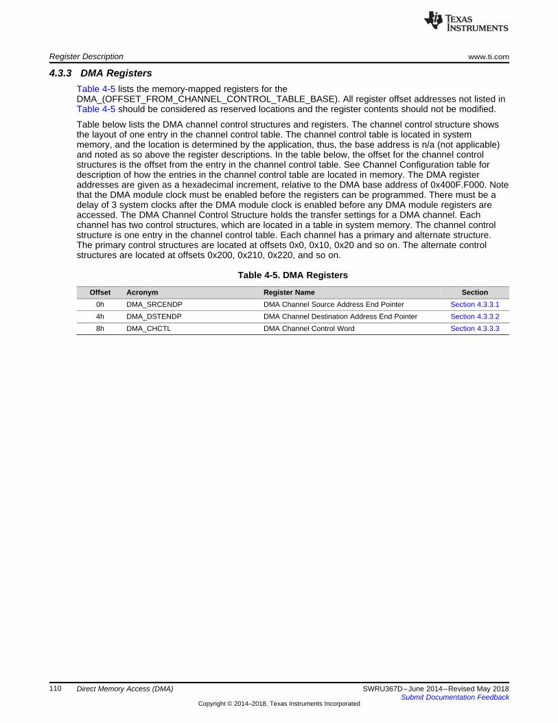
Register Description www.ti.com
110 SWRU367D–June 2014–Revised May 2018Submit Documentation Feedback
Copyright © 2014–2018, Texas Instruments Incorporated
Direct Memory Access (DMA)
4.3.3 DMA RegistersTable 4-5 lists the memory-mapped registers for theDMA_(OFFSET_FROM_CHANNEL_CONTROL_TABLE_BASE). All register offset addresses not listed inTable 4-5 should be considered as reserved locations and the register contents should not be modified.
Table below lists the DMA channel control structures and registers. The channel control structure showsthe layout of one entry in the channel control table. The channel control table is located in systemmemory, and the location is determined by the application, thus, the base address is n/a (not applicable)and noted as so above the register descriptions. In the table below, the offset for the channel controlstructures is the offset from the entry in the channel control table. See Channel Configuration table fordescription of how the entries in the channel control table are located in memory. The DMA registeraddresses are given as a hexadecimal increment, relative to the DMA base address of 0x400F.F000. Notethat the DMA module clock must be enabled before the registers can be programmed. There must be adelay of 3 system clocks after the DMA module clock is enabled before any DMA module registers areaccessed. The DMA Channel Control Structure holds the transfer settings for a DMA channel. Eachchannel has two control structures, which are located in a table in system memory. The channel controlstructure is one entry in the channel control table. Each channel has a primary and alternate structure.The primary control structures are located at offsets 0x0, 0x10, 0x20 and so on. The alternate controlstructures are located at offsets 0x200, 0x210, 0x220, and so on.
Table 4-5. DMA Registers
Offset Acronym Register Name Section0h DMA_SRCENDP DMA Channel Source Address End Pointer Section 4.3.3.14h DMA_DSTENDP DMA Channel Destination Address End Pointer Section 4.3.3.28h DMA_CHCTL DMA Channel Control Word Section 4.3.3.3
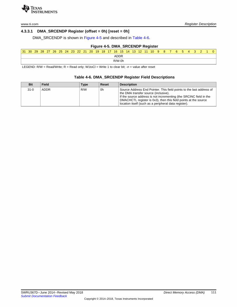
www.ti.com Register Description
111SWRU367D–June 2014–Revised May 2018Submit Documentation Feedback
Copyright © 2014–2018, Texas Instruments Incorporated
Direct Memory Access (DMA)
4.3.3.1 DMA_SRCENDP Register (offset = 0h) [reset = 0h]DMA_SRCENDP is shown in Figure 4-5 and described in Table 4-6.
Figure 4-5. DMA_SRCENDP Register31 30 29 28 27 26 25 24 23 22 21 20 19 18 17 16 15 14 13 12 11 10 9 8 7 6 5 4 3 2 1 0
ADDRR/W-0h
LEGEND: R/W = Read/Write; R = Read only; W1toCl = Write 1 to clear bit; -n = value after reset
Table 4-6. DMA_SRCENDP Register Field Descriptions
Bit Field Type Reset Description31-0 ADDR R/W 0h Source Address End Pointer. This field points to the last address of
the DMA transfer source (inclusive).If the source address is not incrementing (the SRCINC field in theDMACHCTL register is 0x3), then this field points at the sourcelocation itself (such as a peripheral data register).
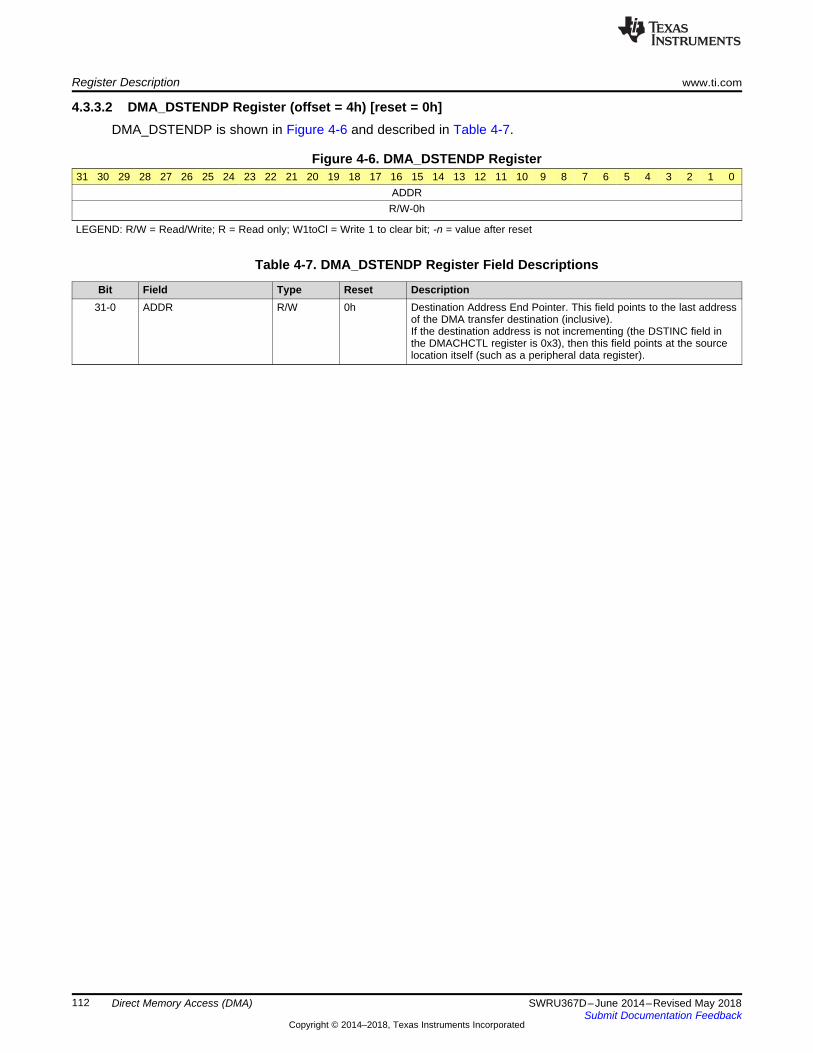
Register Description www.ti.com
112 SWRU367D–June 2014–Revised May 2018Submit Documentation Feedback
Copyright © 2014–2018, Texas Instruments Incorporated
Direct Memory Access (DMA)
4.3.3.2 DMA_DSTENDP Register (offset = 4h) [reset = 0h]DMA_DSTENDP is shown in Figure 4-6 and described in Table 4-7.
Figure 4-6. DMA_DSTENDP Register31 30 29 28 27 26 25 24 23 22 21 20 19 18 17 16 15 14 13 12 11 10 9 8 7 6 5 4 3 2 1 0
ADDRR/W-0h
LEGEND: R/W = Read/Write; R = Read only; W1toCl = Write 1 to clear bit; -n = value after reset
Table 4-7. DMA_DSTENDP Register Field Descriptions
Bit Field Type Reset Description31-0 ADDR R/W 0h Destination Address End Pointer. This field points to the last address
of the DMA transfer destination (inclusive).If the destination address is not incrementing (the DSTINC field inthe DMACHCTL register is 0x3), then this field points at the sourcelocation itself (such as a peripheral data register).
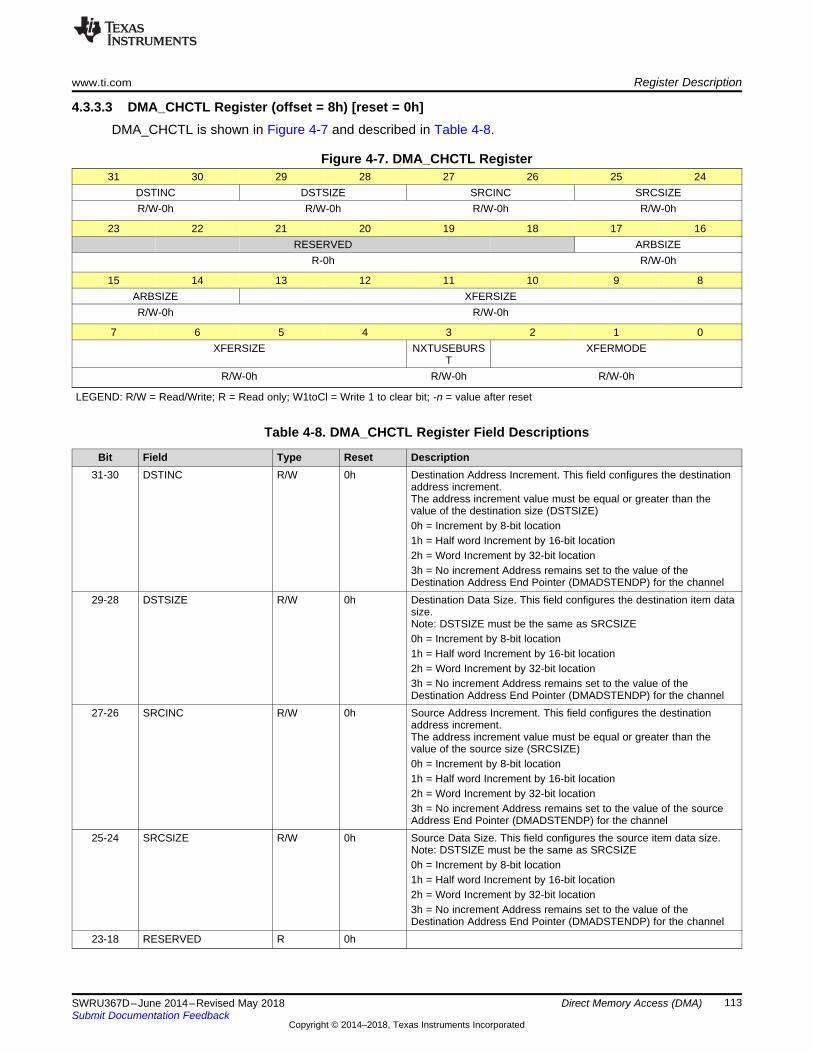
www.ti.com Register Description
113SWRU367D–June 2014–Revised May 2018Submit Documentation Feedback
Copyright © 2014–2018, Texas Instruments Incorporated
Direct Memory Access (DMA)
4.3.3.3 DMA_CHCTL Register (offset = 8h) [reset = 0h]DMA_CHCTL is shown in Figure 4-7 and described in Table 4-8.
Figure 4-7. DMA_CHCTL Register31 30 29 28 27 26 25 24
DSTINC DSTSIZE SRCINC SRCSIZER/W-0h R/W-0h R/W-0h R/W-0h
23 22 21 20 19 18 17 16RESERVED ARBSIZE
R-0h R/W-0h
15 14 13 12 11 10 9 8ARBSIZE XFERSIZER/W-0h R/W-0h
7 6 5 4 3 2 1 0XFERSIZE NXTUSEBURS
TXFERMODE
R/W-0h R/W-0h R/W-0h
LEGEND: R/W = Read/Write; R = Read only; W1toCl = Write 1 to clear bit; -n = value after reset
Table 4-8. DMA_CHCTL Register Field Descriptions
Bit Field Type Reset Description31-30 DSTINC R/W 0h Destination Address Increment. This field configures the destination
address increment.The address increment value must be equal or greater than thevalue of the destination size (DSTSIZE)0h = Increment by 8-bit location1h = Half word Increment by 16-bit location2h = Word Increment by 32-bit location3h = No increment Address remains set to the value of theDestination Address End Pointer (DMADSTENDP) for the channel
29-28 DSTSIZE R/W 0h Destination Data Size. This field configures the destination item datasize.Note: DSTSIZE must be the same as SRCSIZE0h = Increment by 8-bit location1h = Half word Increment by 16-bit location2h = Word Increment by 32-bit location3h = No increment Address remains set to the value of theDestination Address End Pointer (DMADSTENDP) for the channel
27-26 SRCINC R/W 0h Source Address Increment. This field configures the destinationaddress increment.The address increment value must be equal or greater than thevalue of the source size (SRCSIZE)0h = Increment by 8-bit location1h = Half word Increment by 16-bit location2h = Word Increment by 32-bit location3h = No increment Address remains set to the value of the sourceAddress End Pointer (DMADSTENDP) for the channel
25-24 SRCSIZE R/W 0h Source Data Size. This field configures the source item data size.Note: DSTSIZE must be the same as SRCSIZE0h = Increment by 8-bit location1h = Half word Increment by 16-bit location2h = Word Increment by 32-bit location3h = No increment Address remains set to the value of theDestination Address End Pointer (DMADSTENDP) for the channel
23-18 RESERVED R 0h
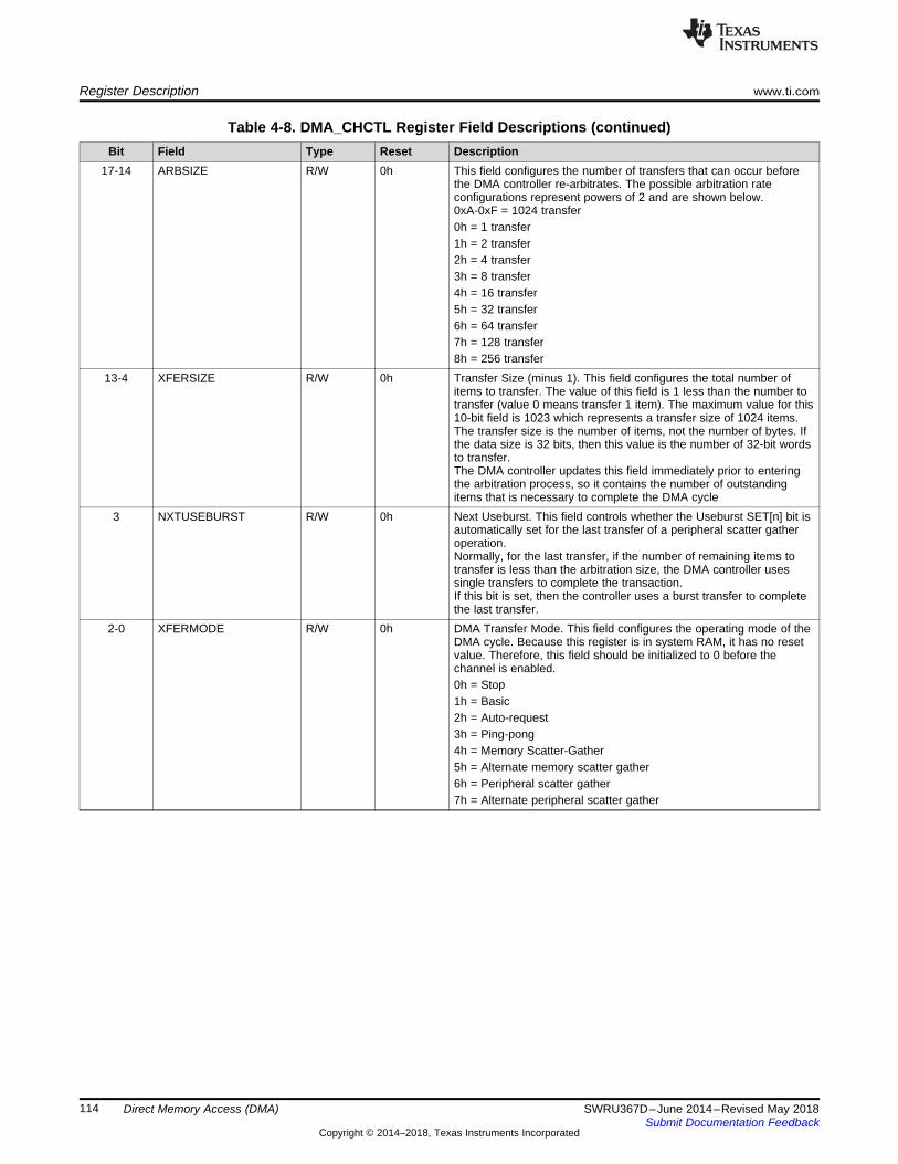
Register Description www.ti.com
114 SWRU367D–June 2014–Revised May 2018Submit Documentation Feedback
Copyright © 2014–2018, Texas Instruments Incorporated
Direct Memory Access (DMA)
Table 4-8. DMA_CHCTL Register Field Descriptions (continued)Bit Field Type Reset Description
17-14 ARBSIZE R/W 0h This field configures the number of transfers that can occur beforethe DMA controller re-arbitrates. The possible arbitration rateconfigurations represent powers of 2 and are shown below.0xA-0xF = 1024 transfer0h = 1 transfer1h = 2 transfer2h = 4 transfer3h = 8 transfer4h = 16 transfer5h = 32 transfer6h = 64 transfer7h = 128 transfer8h = 256 transfer
13-4 XFERSIZE R/W 0h Transfer Size (minus 1). This field configures the total number ofitems to transfer. The value of this field is 1 less than the number totransfer (value 0 means transfer 1 item). The maximum value for this10-bit field is 1023 which represents a transfer size of 1024 items.The transfer size is the number of items, not the number of bytes. Ifthe data size is 32 bits, then this value is the number of 32-bit wordsto transfer.The DMA controller updates this field immediately prior to enteringthe arbitration process, so it contains the number of outstandingitems that is necessary to complete the DMA cycle
3 NXTUSEBURST R/W 0h Next Useburst. This field controls whether the Useburst SET[n] bit isautomatically set for the last transfer of a peripheral scatter gatheroperation.Normally, for the last transfer, if the number of remaining items totransfer is less than the arbitration size, the DMA controller usessingle transfers to complete the transaction.If this bit is set, then the controller uses a burst transfer to completethe last transfer.
2-0 XFERMODE R/W 0h DMA Transfer Mode. This field configures the operating mode of theDMA cycle. Because this register is in system RAM, it has no resetvalue. Therefore, this field should be initialized to 0 before thechannel is enabled.0h = Stop1h = Basic2h = Auto-request3h = Ping-pong4h = Memory Scatter-Gather5h = Alternate memory scatter gather6h = Peripheral scatter gather7h = Alternate peripheral scatter gather
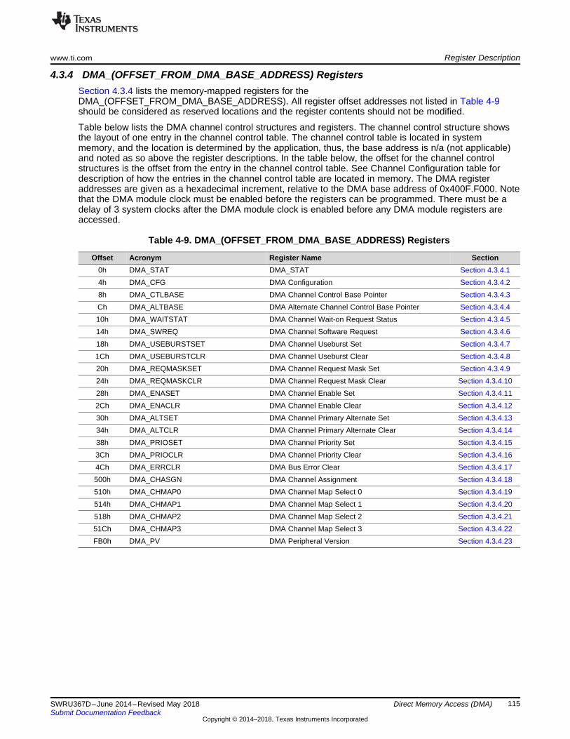
www.ti.com Register Description
115SWRU367D–June 2014–Revised May 2018Submit Documentation Feedback
Copyright © 2014–2018, Texas Instruments Incorporated
Direct Memory Access (DMA)
4.3.4 DMA_(OFFSET_FROM_DMA_BASE_ADDRESS) RegistersSection 4.3.4 lists the memory-mapped registers for theDMA_(OFFSET_FROM_DMA_BASE_ADDRESS). All register offset addresses not listed in Table 4-9should be considered as reserved locations and the register contents should not be modified.
Table below lists the DMA channel control structures and registers. The channel control structure showsthe layout of one entry in the channel control table. The channel control table is located in systemmemory, and the location is determined by the application, thus, the base address is n/a (not applicable)and noted as so above the register descriptions. In the table below, the offset for the channel controlstructures is the offset from the entry in the channel control table. See Channel Configuration table fordescription of how the entries in the channel control table are located in memory. The DMA registeraddresses are given as a hexadecimal increment, relative to the DMA base address of 0x400F.F000. Notethat the DMA module clock must be enabled before the registers can be programmed. There must be adelay of 3 system clocks after the DMA module clock is enabled before any DMA module registers areaccessed.
Table 4-9. DMA_(OFFSET_FROM_DMA_BASE_ADDRESS) Registers
Offset Acronym Register Name Section0h DMA_STAT DMA_STAT Section 4.3.4.14h DMA_CFG DMA Configuration Section 4.3.4.28h DMA_CTLBASE DMA Channel Control Base Pointer Section 4.3.4.3Ch DMA_ALTBASE DMA Alternate Channel Control Base Pointer Section 4.3.4.410h DMA_WAITSTAT DMA Channel Wait-on Request Status Section 4.3.4.514h DMA_SWREQ DMA Channel Software Request Section 4.3.4.618h DMA_USEBURSTSET DMA Channel Useburst Set Section 4.3.4.71Ch DMA_USEBURSTCLR DMA Channel Useburst Clear Section 4.3.4.820h DMA_REQMASKSET DMA Channel Request Mask Set Section 4.3.4.924h DMA_REQMASKCLR DMA Channel Request Mask Clear Section 4.3.4.1028h DMA_ENASET DMA Channel Enable Set Section 4.3.4.112Ch DMA_ENACLR DMA Channel Enable Clear Section 4.3.4.1230h DMA_ALTSET DMA Channel Primary Alternate Set Section 4.3.4.1334h DMA_ALTCLR DMA Channel Primary Alternate Clear Section 4.3.4.1438h DMA_PRIOSET DMA Channel Priority Set Section 4.3.4.153Ch DMA_PRIOCLR DMA Channel Priority Clear Section 4.3.4.164Ch DMA_ERRCLR DMA Bus Error Clear Section 4.3.4.17500h DMA_CHASGN DMA Channel Assignment Section 4.3.4.18510h DMA_CHMAP0 DMA Channel Map Select 0 Section 4.3.4.19514h DMA_CHMAP1 DMA Channel Map Select 1 Section 4.3.4.20518h DMA_CHMAP2 DMA Channel Map Select 2 Section 4.3.4.2151Ch DMA_CHMAP3 DMA Channel Map Select 3 Section 4.3.4.22FB0h DMA_PV DMA Peripheral Version Section 4.3.4.23
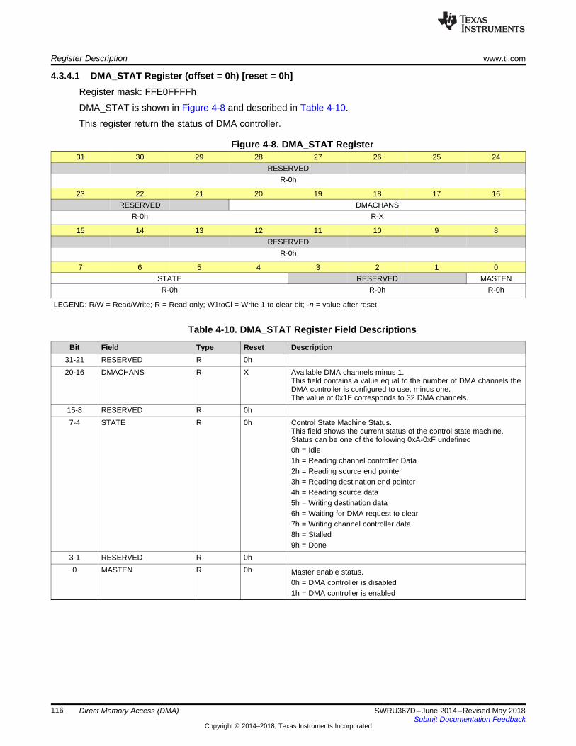
Register Description www.ti.com
116 SWRU367D–June 2014–Revised May 2018Submit Documentation Feedback
Copyright © 2014–2018, Texas Instruments Incorporated
Direct Memory Access (DMA)
4.3.4.1 DMA_STAT Register (offset = 0h) [reset = 0h]Register mask: FFE0FFFFh
DMA_STAT is shown in Figure 4-8 and described in Table 4-10.
This register return the status of DMA controller.
Figure 4-8. DMA_STAT Register31 30 29 28 27 26 25 24
RESERVEDR-0h
23 22 21 20 19 18 17 16RESERVED DMACHANS
R-0h R-X
15 14 13 12 11 10 9 8RESERVED
R-0h
7 6 5 4 3 2 1 0STATE RESERVED MASTENR-0h R-0h R-0h
LEGEND: R/W = Read/Write; R = Read only; W1toCl = Write 1 to clear bit; -n = value after reset
Table 4-10. DMA_STAT Register Field Descriptions
Bit Field Type Reset Description31-21 RESERVED R 0h20-16 DMACHANS R X Available DMA channels minus 1.
This field contains a value equal to the number of DMA channels theDMA controller is configured to use, minus one.The value of 0x1F corresponds to 32 DMA channels.
15-8 RESERVED R 0h7-4 STATE R 0h Control State Machine Status.
This field shows the current status of the control state machine.Status can be one of the following 0xA-0xF undefined0h = Idle1h = Reading channel controller Data2h = Reading source end pointer3h = Reading destination end pointer4h = Reading source data5h = Writing destination data6h = Waiting for DMA request to clear7h = Writing channel controller data8h = Stalled9h = Done
3-1 RESERVED R 0h0 MASTEN R 0h Master enable status.
0h = DMA controller is disabled1h = DMA controller is enabled
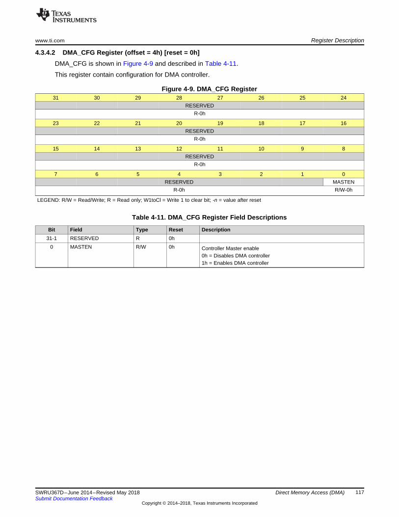
www.ti.com Register Description
117SWRU367D–June 2014–Revised May 2018Submit Documentation Feedback
Copyright © 2014–2018, Texas Instruments Incorporated
Direct Memory Access (DMA)
4.3.4.2 DMA_CFG Register (offset = 4h) [reset = 0h]DMA_CFG is shown in Figure 4-9 and described in Table 4-11.
This register contain configuration for DMA controller.
Figure 4-9. DMA_CFG Register31 30 29 28 27 26 25 24
RESERVEDR-0h
23 22 21 20 19 18 17 16RESERVED
R-0h
15 14 13 12 11 10 9 8RESERVED
R-0h
7 6 5 4 3 2 1 0RESERVED MASTEN
R-0h R/W-0h
LEGEND: R/W = Read/Write; R = Read only; W1toCl = Write 1 to clear bit; -n = value after reset
Table 4-11. DMA_CFG Register Field Descriptions
Bit Field Type Reset Description31-1 RESERVED R 0h
0 MASTEN R/W 0h Controller Master enable0h = Disables DMA controller1h = Enables DMA controller
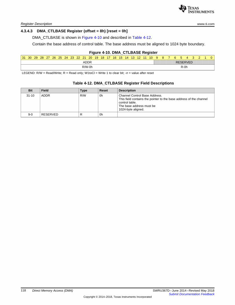
Register Description www.ti.com
118 SWRU367D–June 2014–Revised May 2018Submit Documentation Feedback
Copyright © 2014–2018, Texas Instruments Incorporated
Direct Memory Access (DMA)
4.3.4.3 DMA_CTLBASE Register (offset = 8h) [reset = 0h]DMA_CTLBASE is shown in Figure 4-10 and described in Table 4-12.
Contain the base address of control table. The base address must be aligned to 1024 byte boundary.
Figure 4-10. DMA_CTLBASE Register31 30 29 28 27 26 25 24 23 22 21 20 19 18 17 16 15 14 13 12 11 10 9 8 7 6 5 4 3 2 1 0
ADDR RESERVEDR/W-0h R-0h
LEGEND: R/W = Read/Write; R = Read only; W1toCl = Write 1 to clear bit; -n = value after reset
Table 4-12. DMA_CTLBASE Register Field Descriptions
Bit Field Type Reset Description31-10 ADDR R/W 0h Channel Control Base Address.
This field contains the pointer to the base address of the channelcontrol table.The base address must be1024-byte aligned.
9-0 RESERVED R 0h
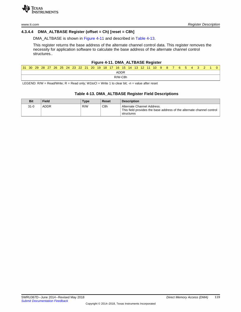
www.ti.com Register Description
119SWRU367D–June 2014–Revised May 2018Submit Documentation Feedback
Copyright © 2014–2018, Texas Instruments Incorporated
Direct Memory Access (DMA)
4.3.4.4 DMA_ALTBASE Register (offset = Ch) [reset = C8h]DMA_ALTBASE is shown in Figure 4-11 and described in Table 4-13.
This register returns the base address of the alternate channel control data. This register removes thenecessity for application software to calculate the base address of the alternate channel controlstructures..
Figure 4-11. DMA_ALTBASE Register31 30 29 28 27 26 25 24 23 22 21 20 19 18 17 16 15 14 13 12 11 10 9 8 7 6 5 4 3 2 1 0
ADDRR/W-C8h
LEGEND: R/W = Read/Write; R = Read only; W1toCl = Write 1 to clear bit; -n = value after reset
Table 4-13. DMA_ALTBASE Register Field Descriptions
Bit Field Type Reset Description31-0 ADDR R/W C8h Alternate Channel Address.
This field provides the base address of the alternate channel controlstructures
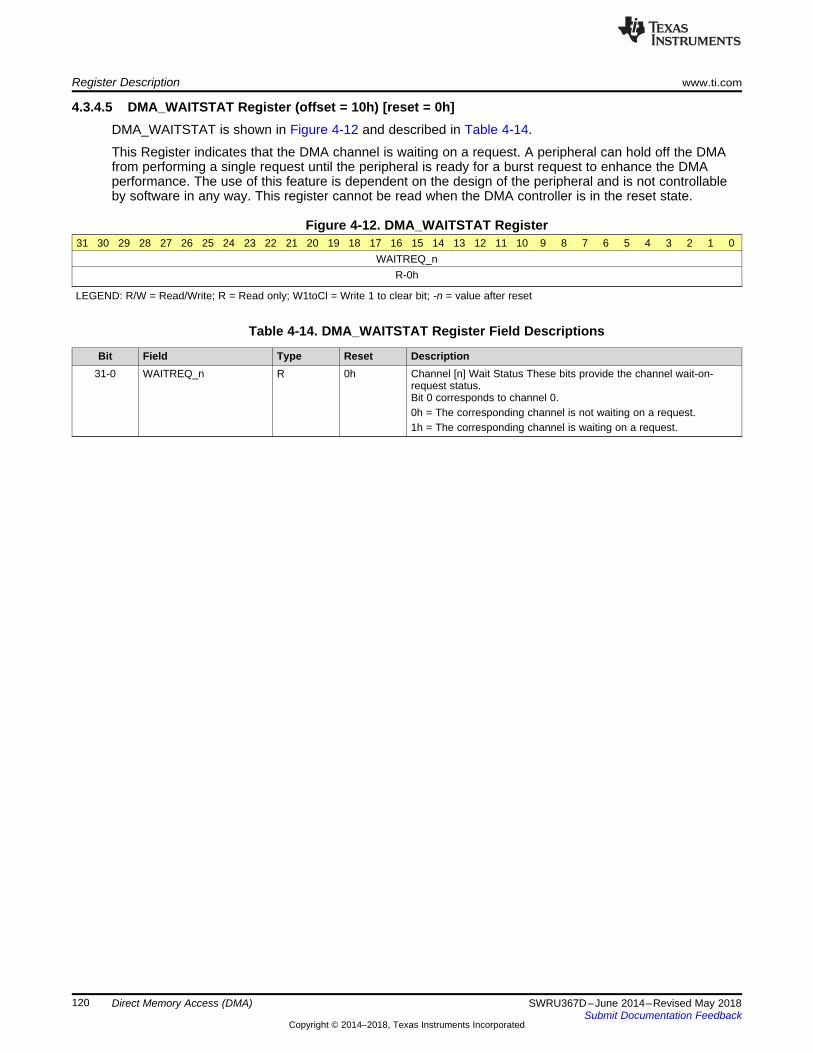
Register Description www.ti.com
120 SWRU367D–June 2014–Revised May 2018Submit Documentation Feedback
Copyright © 2014–2018, Texas Instruments Incorporated
Direct Memory Access (DMA)
4.3.4.5 DMA_WAITSTAT Register (offset = 10h) [reset = 0h]DMA_WAITSTAT is shown in Figure 4-12 and described in Table 4-14.
This Register indicates that the DMA channel is waiting on a request. A peripheral can hold off the DMAfrom performing a single request until the peripheral is ready for a burst request to enhance the DMAperformance. The use of this feature is dependent on the design of the peripheral and is not controllableby software in any way. This register cannot be read when the DMA controller is in the reset state.
Figure 4-12. DMA_WAITSTAT Register31 30 29 28 27 26 25 24 23 22 21 20 19 18 17 16 15 14 13 12 11 10 9 8 7 6 5 4 3 2 1 0
WAITREQ_nR-0h
LEGEND: R/W = Read/Write; R = Read only; W1toCl = Write 1 to clear bit; -n = value after reset
Table 4-14. DMA_WAITSTAT Register Field Descriptions
Bit Field Type Reset Description31-0 WAITREQ_n R 0h Channel [n] Wait Status These bits provide the channel wait-on-
request status.Bit 0 corresponds to channel 0.0h = The corresponding channel is not waiting on a request.1h = The corresponding channel is waiting on a request.
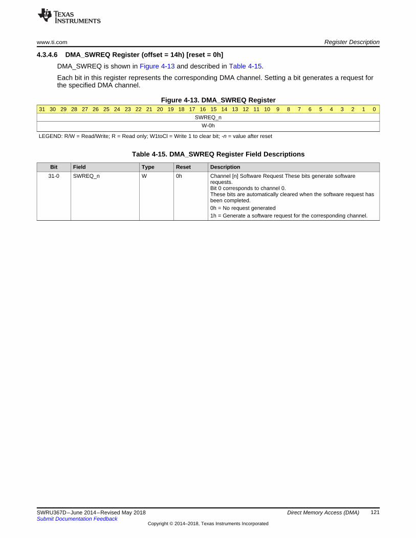
www.ti.com Register Description
121SWRU367D–June 2014–Revised May 2018Submit Documentation Feedback
Copyright © 2014–2018, Texas Instruments Incorporated
Direct Memory Access (DMA)
4.3.4.6 DMA_SWREQ Register (offset = 14h) [reset = 0h]DMA_SWREQ is shown in Figure 4-13 and described in Table 4-15.
Each bit in this register represents the corresponding DMA channel. Setting a bit generates a request forthe specified DMA channel.
Figure 4-13. DMA_SWREQ Register31 30 29 28 27 26 25 24 23 22 21 20 19 18 17 16 15 14 13 12 11 10 9 8 7 6 5 4 3 2 1 0
SWREQ_nW-0h
LEGEND: R/W = Read/Write; R = Read only; W1toCl = Write 1 to clear bit; -n = value after reset
Table 4-15. DMA_SWREQ Register Field Descriptions
Bit Field Type Reset Description31-0 SWREQ_n W 0h Channel [n] Software Request These bits generate software
requests.Bit 0 corresponds to channel 0.These bits are automatically cleared when the software request hasbeen completed.0h = No request generated1h = Generate a software request for the corresponding channel.
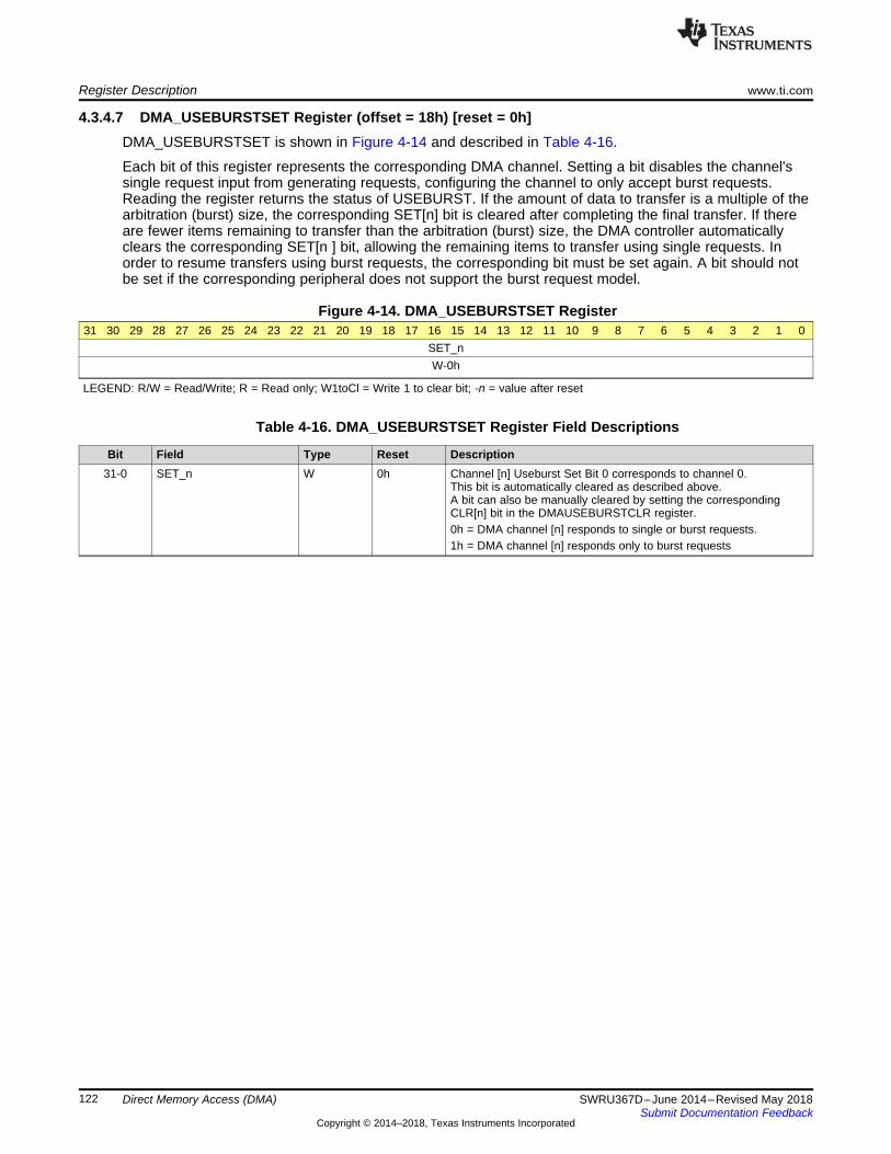
Register Description www.ti.com
122 SWRU367D–June 2014–Revised May 2018Submit Documentation Feedback
Copyright © 2014–2018, Texas Instruments Incorporated
Direct Memory Access (DMA)
4.3.4.7 DMA_USEBURSTSET Register (offset = 18h) [reset = 0h]DMA_USEBURSTSET is shown in Figure 4-14 and described in Table 4-16.
Each bit of this register represents the corresponding DMA channel. Setting a bit disables the channel'ssingle request input from generating requests, configuring the channel to only accept burst requests.Reading the register returns the status of USEBURST. If the amount of data to transfer is a multiple of thearbitration (burst) size, the corresponding SET[n] bit is cleared after completing the final transfer. If thereare fewer items remaining to transfer than the arbitration (burst) size, the DMA controller automaticallyclears the corresponding SET[n ] bit, allowing the remaining items to transfer using single requests. Inorder to resume transfers using burst requests, the corresponding bit must be set again. A bit should notbe set if the corresponding peripheral does not support the burst request model.
Figure 4-14. DMA_USEBURSTSET Register31 30 29 28 27 26 25 24 23 22 21 20 19 18 17 16 15 14 13 12 11 10 9 8 7 6 5 4 3 2 1 0
SET_nW-0h
LEGEND: R/W = Read/Write; R = Read only; W1toCl = Write 1 to clear bit; -n = value after reset
Table 4-16. DMA_USEBURSTSET Register Field Descriptions
Bit Field Type Reset Description31-0 SET_n W 0h Channel [n] Useburst Set Bit 0 corresponds to channel 0.
This bit is automatically cleared as described above.A bit can also be manually cleared by setting the correspondingCLR[n] bit in the DMAUSEBURSTCLR register.0h = DMA channel [n] responds to single or burst requests.1h = DMA channel [n] responds only to burst requests
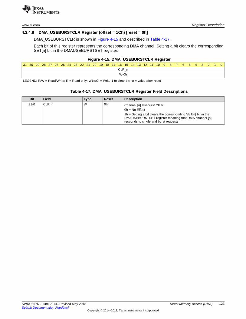
www.ti.com Register Description
123SWRU367D–June 2014–Revised May 2018Submit Documentation Feedback
Copyright © 2014–2018, Texas Instruments Incorporated
Direct Memory Access (DMA)
4.3.4.8 DMA_USEBURSTCLR Register (offset = 1Ch) [reset = 0h]DMA_USEBURSTCLR is shown in Figure 4-15 and described in Table 4-17.
Each bit of this register represents the corresponding DMA channel. Setting a bit clears the correspondingSET[n] bit in the DMAUSEBURSTSET register.
Figure 4-15. DMA_USEBURSTCLR Register31 30 29 28 27 26 25 24 23 22 21 20 19 18 17 16 15 14 13 12 11 10 9 8 7 6 5 4 3 2 1 0
CLR_nW-0h
LEGEND: R/W = Read/Write; R = Read only; W1toCl = Write 1 to clear bit; -n = value after reset
Table 4-17. DMA_USEBURSTCLR Register Field Descriptions
Bit Field Type Reset Description31-0 CLR_n W 0h Channel [n] Useburst Clear
0h = No Effect1h = Setting a bit clears the corresponding SET[n] bit in theDMAUSEBURSTSET register meaning that DMA channel [n]responds to single and burst requests
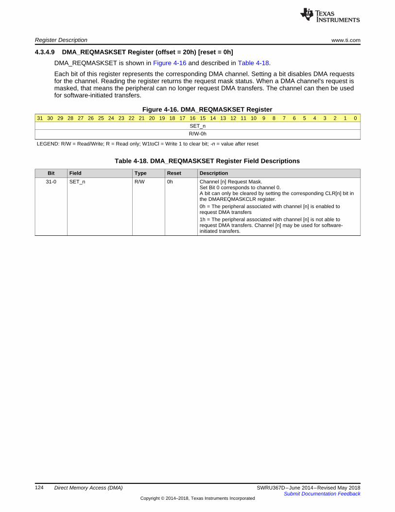
Register Description www.ti.com
124 SWRU367D–June 2014–Revised May 2018Submit Documentation Feedback
Copyright © 2014–2018, Texas Instruments Incorporated
Direct Memory Access (DMA)
4.3.4.9 DMA_REQMASKSET Register (offset = 20h) [reset = 0h]DMA_REQMASKSET is shown in Figure 4-16 and described in Table 4-18.
Each bit of this register represents the corresponding DMA channel. Setting a bit disables DMA requestsfor the channel. Reading the register returns the request mask status. When a DMA channel's request ismasked, that means the peripheral can no longer request DMA transfers. The channel can then be usedfor software-initiated transfers.
Figure 4-16. DMA_REQMASKSET Register31 30 29 28 27 26 25 24 23 22 21 20 19 18 17 16 15 14 13 12 11 10 9 8 7 6 5 4 3 2 1 0
SET_nR/W-0h
LEGEND: R/W = Read/Write; R = Read only; W1toCl = Write 1 to clear bit; -n = value after reset
Table 4-18. DMA_REQMASKSET Register Field Descriptions
Bit Field Type Reset Description31-0 SET_n R/W 0h Channel [n] Request Mask.
Set Bit 0 corresponds to channel 0.A bit can only be cleared by setting the corresponding CLR[n] bit inthe DMAREQMASKCLR register.0h = The peripheral associated with channel [n] is enabled torequest DMA transfers1h = The peripheral associated with channel [n] is not able torequest DMA transfers. Channel [n] may be used for software-initiated transfers.
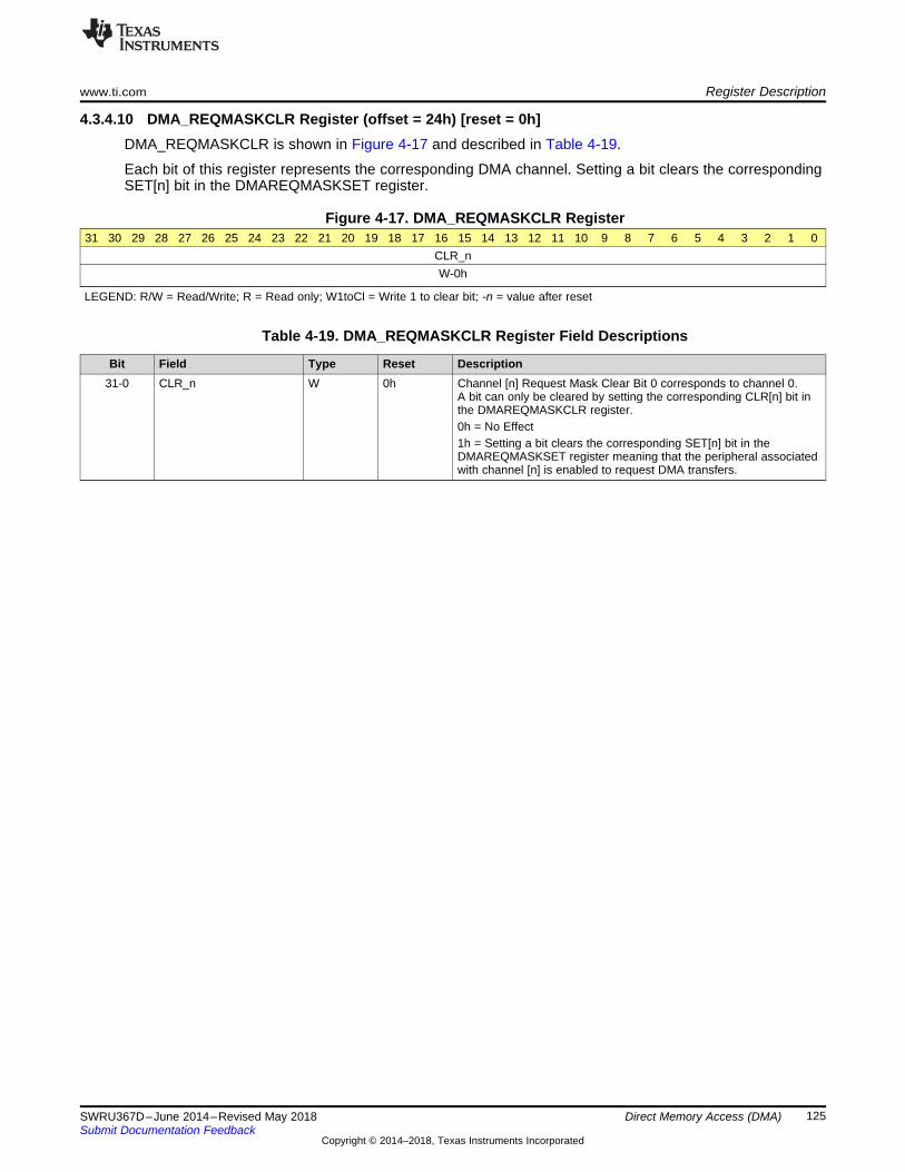
www.ti.com Register Description
125SWRU367D–June 2014–Revised May 2018Submit Documentation Feedback
Copyright © 2014–2018, Texas Instruments Incorporated
Direct Memory Access (DMA)
4.3.4.10 DMA_REQMASKCLR Register (offset = 24h) [reset = 0h]DMA_REQMASKCLR is shown in Figure 4-17 and described in Table 4-19.
Each bit of this register represents the corresponding DMA channel. Setting a bit clears the correspondingSET[n] bit in the DMAREQMASKSET register.
Figure 4-17. DMA_REQMASKCLR Register31 30 29 28 27 26 25 24 23 22 21 20 19 18 17 16 15 14 13 12 11 10 9 8 7 6 5 4 3 2 1 0
CLR_nW-0h
LEGEND: R/W = Read/Write; R = Read only; W1toCl = Write 1 to clear bit; -n = value after reset
Table 4-19. DMA_REQMASKCLR Register Field Descriptions
Bit Field Type Reset Description31-0 CLR_n W 0h Channel [n] Request Mask Clear Bit 0 corresponds to channel 0.
A bit can only be cleared by setting the corresponding CLR[n] bit inthe DMAREQMASKCLR register.0h = No Effect1h = Setting a bit clears the corresponding SET[n] bit in theDMAREQMASKSET register meaning that the peripheral associatedwith channel [n] is enabled to request DMA transfers.
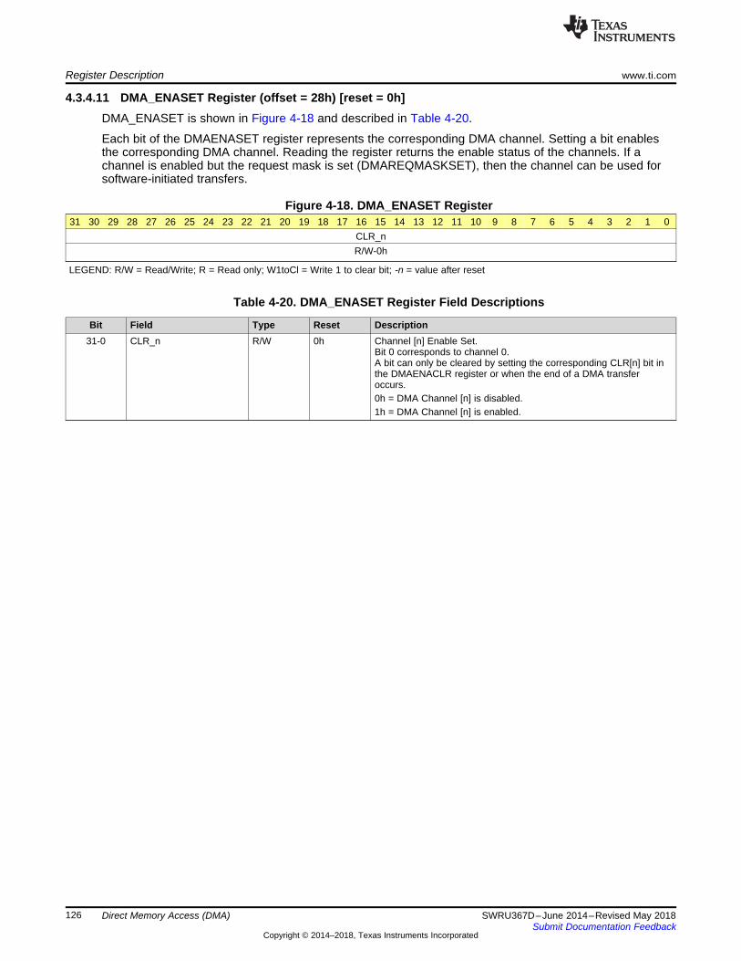
Register Description www.ti.com
126 SWRU367D–June 2014–Revised May 2018Submit Documentation Feedback
Copyright © 2014–2018, Texas Instruments Incorporated
Direct Memory Access (DMA)
4.3.4.11 DMA_ENASET Register (offset = 28h) [reset = 0h]DMA_ENASET is shown in Figure 4-18 and described in Table 4-20.
Each bit of the DMAENASET register represents the corresponding DMA channel. Setting a bit enablesthe corresponding DMA channel. Reading the register returns the enable status of the channels. If achannel is enabled but the request mask is set (DMAREQMASKSET), then the channel can be used forsoftware-initiated transfers.
Figure 4-18. DMA_ENASET Register31 30 29 28 27 26 25 24 23 22 21 20 19 18 17 16 15 14 13 12 11 10 9 8 7 6 5 4 3 2 1 0
CLR_nR/W-0h
LEGEND: R/W = Read/Write; R = Read only; W1toCl = Write 1 to clear bit; -n = value after reset
Table 4-20. DMA_ENASET Register Field Descriptions
Bit Field Type Reset Description31-0 CLR_n R/W 0h Channel [n] Enable Set.
Bit 0 corresponds to channel 0.A bit can only be cleared by setting the corresponding CLR[n] bit inthe DMAENACLR register or when the end of a DMA transferoccurs.0h = DMA Channel [n] is disabled.1h = DMA Channel [n] is enabled.
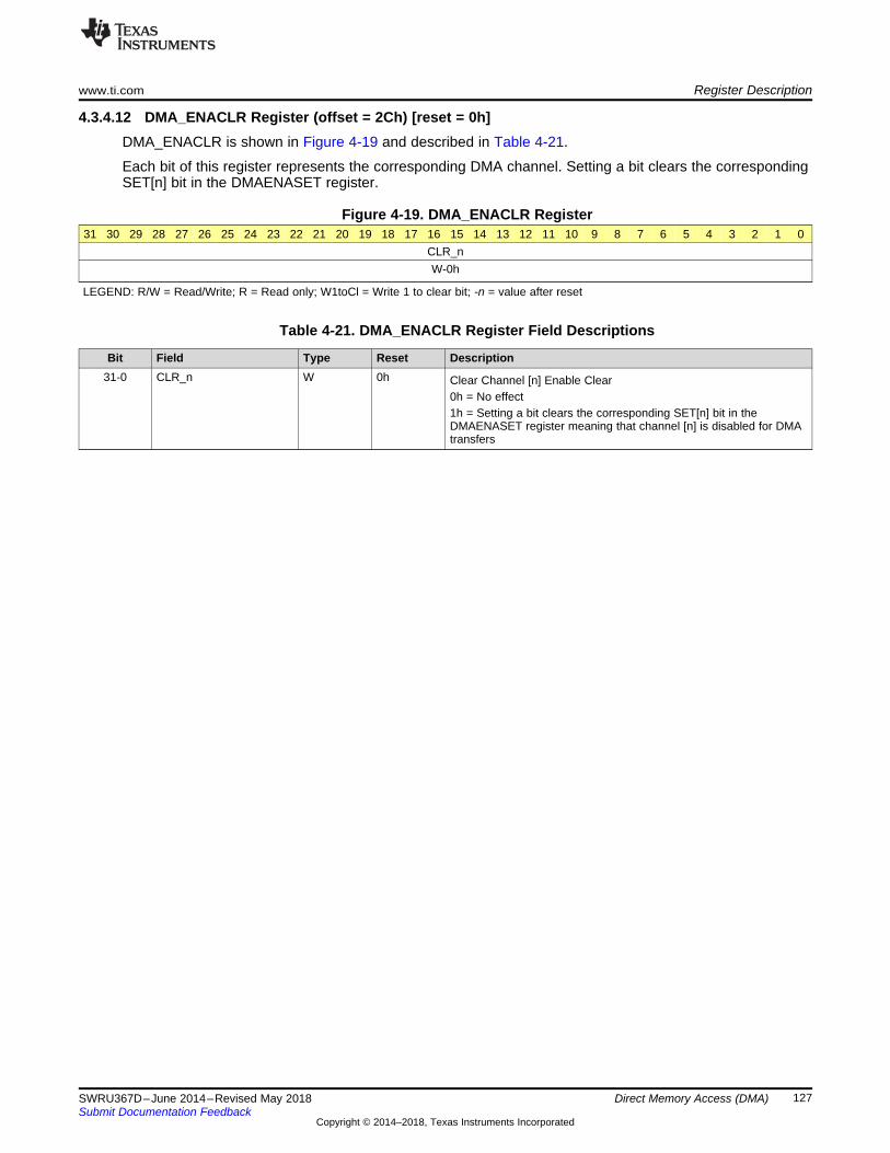
www.ti.com Register Description
127SWRU367D–June 2014–Revised May 2018Submit Documentation Feedback
Copyright © 2014–2018, Texas Instruments Incorporated
Direct Memory Access (DMA)
4.3.4.12 DMA_ENACLR Register (offset = 2Ch) [reset = 0h]DMA_ENACLR is shown in Figure 4-19 and described in Table 4-21.
Each bit of this register represents the corresponding DMA channel. Setting a bit clears the correspondingSET[n] bit in the DMAENASET register.
Figure 4-19. DMA_ENACLR Register31 30 29 28 27 26 25 24 23 22 21 20 19 18 17 16 15 14 13 12 11 10 9 8 7 6 5 4 3 2 1 0
CLR_nW-0h
LEGEND: R/W = Read/Write; R = Read only; W1toCl = Write 1 to clear bit; -n = value after reset
Table 4-21. DMA_ENACLR Register Field Descriptions
Bit Field Type Reset Description31-0 CLR_n W 0h Clear Channel [n] Enable Clear
0h = No effect1h = Setting a bit clears the corresponding SET[n] bit in theDMAENASET register meaning that channel [n] is disabled for DMAtransfers
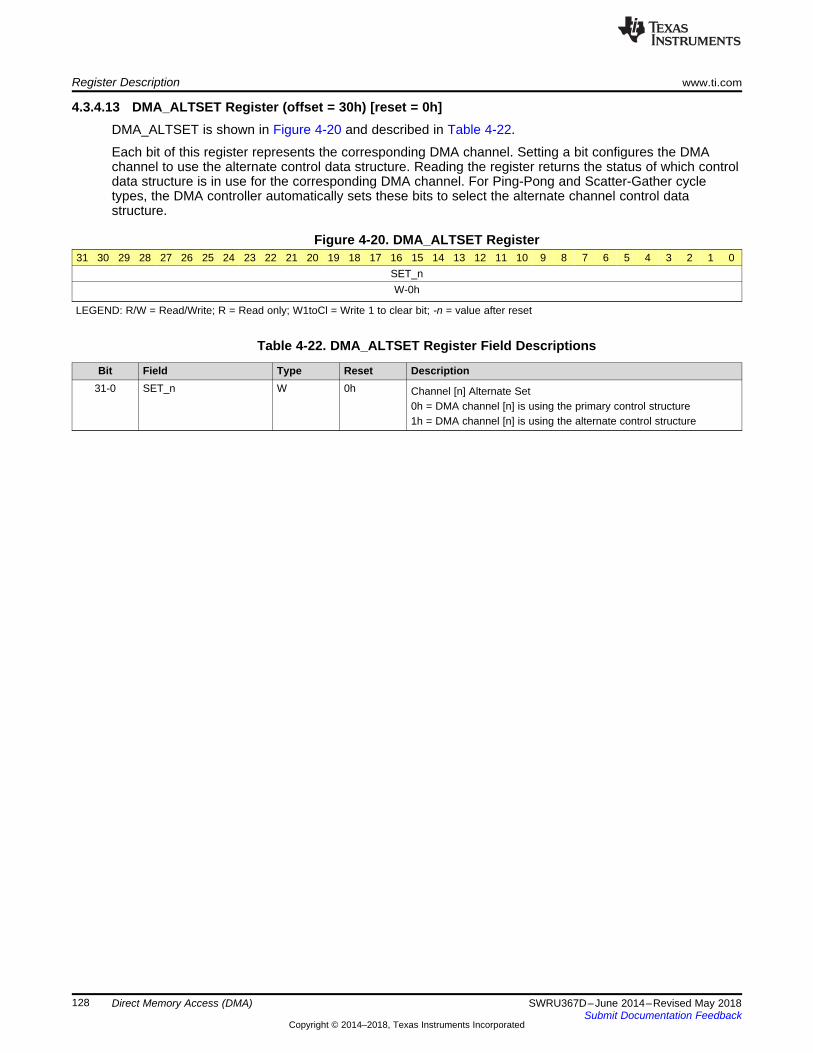
Register Description www.ti.com
128 SWRU367D–June 2014–Revised May 2018Submit Documentation Feedback
Copyright © 2014–2018, Texas Instruments Incorporated
Direct Memory Access (DMA)
4.3.4.13 DMA_ALTSET Register (offset = 30h) [reset = 0h]DMA_ALTSET is shown in Figure 4-20 and described in Table 4-22.
Each bit of this register represents the corresponding DMA channel. Setting a bit configures the DMAchannel to use the alternate control data structure. Reading the register returns the status of which controldata structure is in use for the corresponding DMA channel. For Ping-Pong and Scatter-Gather cycletypes, the DMA controller automatically sets these bits to select the alternate channel control datastructure.
Figure 4-20. DMA_ALTSET Register31 30 29 28 27 26 25 24 23 22 21 20 19 18 17 16 15 14 13 12 11 10 9 8 7 6 5 4 3 2 1 0
SET_nW-0h
LEGEND: R/W = Read/Write; R = Read only; W1toCl = Write 1 to clear bit; -n = value after reset
Table 4-22. DMA_ALTSET Register Field Descriptions
Bit Field Type Reset Description31-0 SET_n W 0h Channel [n] Alternate Set
0h = DMA channel [n] is using the primary control structure1h = DMA channel [n] is using the alternate control structure
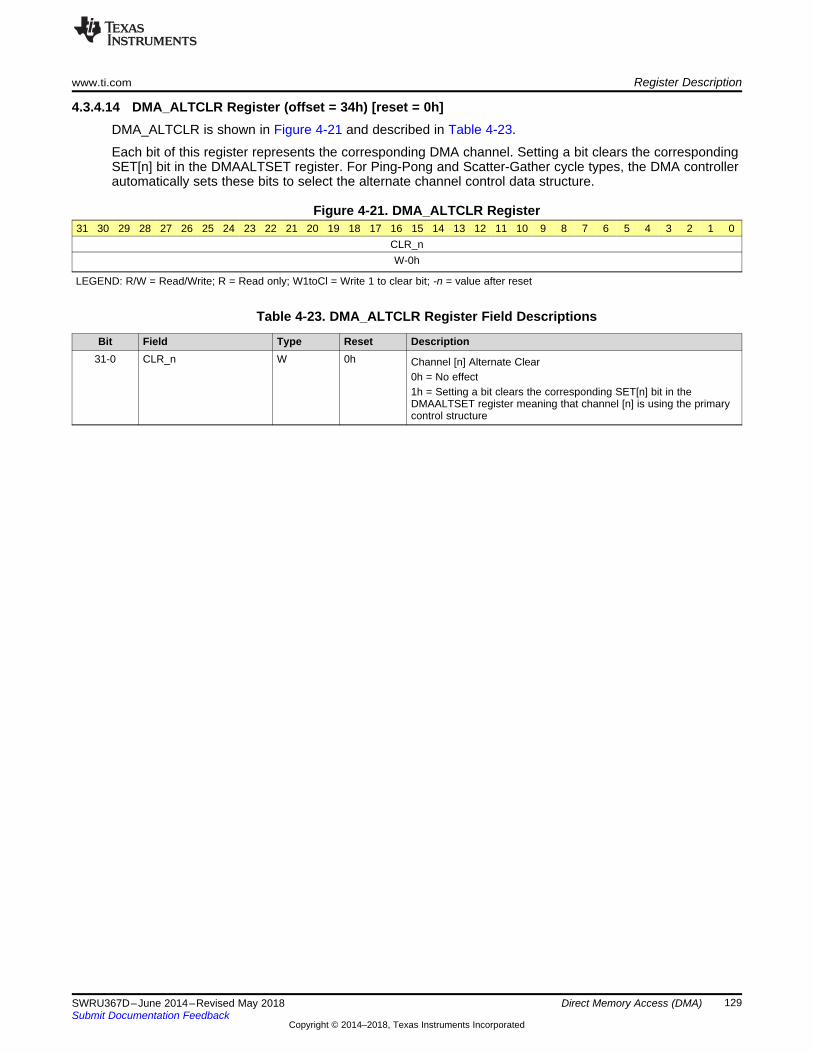
www.ti.com Register Description
129SWRU367D–June 2014–Revised May 2018Submit Documentation Feedback
Copyright © 2014–2018, Texas Instruments Incorporated
Direct Memory Access (DMA)
4.3.4.14 DMA_ALTCLR Register (offset = 34h) [reset = 0h]DMA_ALTCLR is shown in Figure 4-21 and described in Table 4-23.
Each bit of this register represents the corresponding DMA channel. Setting a bit clears the correspondingSET[n] bit in the DMAALTSET register. For Ping-Pong and Scatter-Gather cycle types, the DMA controllerautomatically sets these bits to select the alternate channel control data structure.
Figure 4-21. DMA_ALTCLR Register31 30 29 28 27 26 25 24 23 22 21 20 19 18 17 16 15 14 13 12 11 10 9 8 7 6 5 4 3 2 1 0
CLR_nW-0h
LEGEND: R/W = Read/Write; R = Read only; W1toCl = Write 1 to clear bit; -n = value after reset
Table 4-23. DMA_ALTCLR Register Field Descriptions
Bit Field Type Reset Description31-0 CLR_n W 0h Channel [n] Alternate Clear
0h = No effect1h = Setting a bit clears the corresponding SET[n] bit in theDMAALTSET register meaning that channel [n] is using the primarycontrol structure
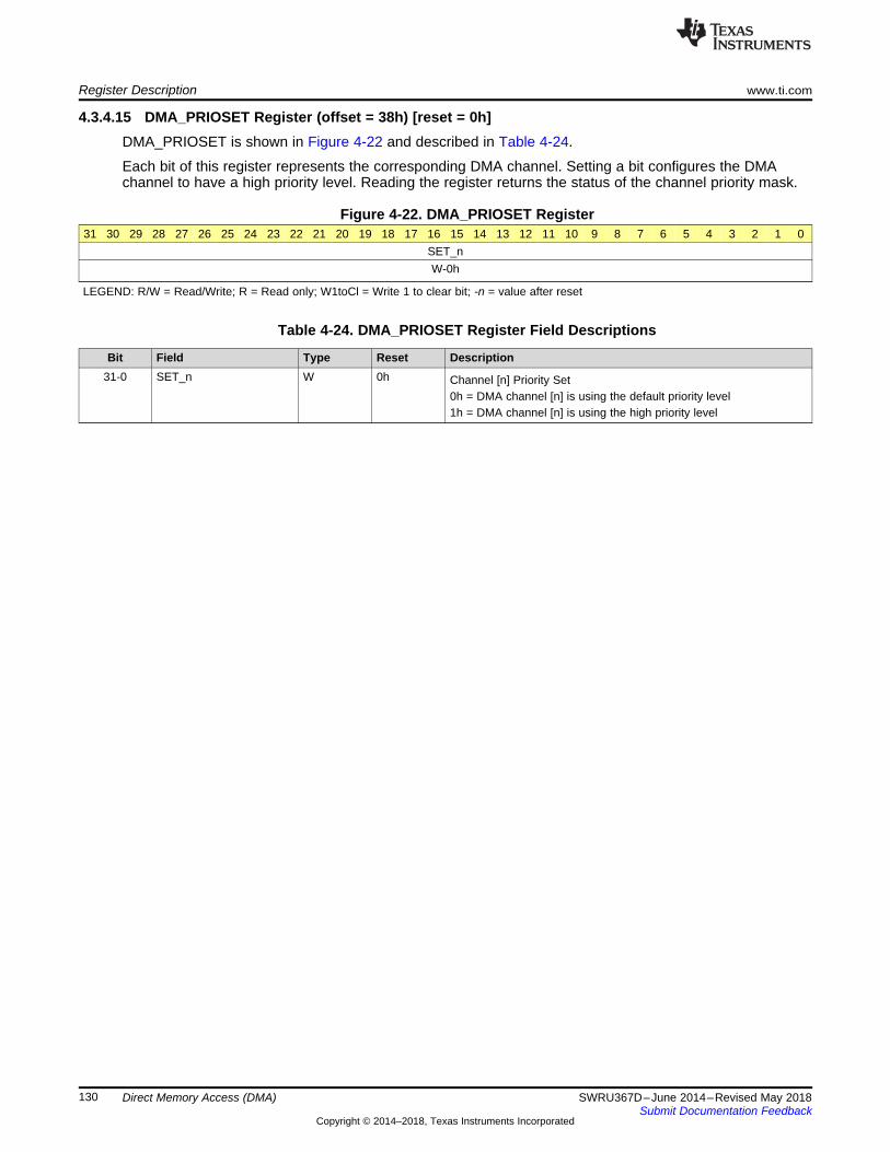
Register Description www.ti.com
130 SWRU367D–June 2014–Revised May 2018Submit Documentation Feedback
Copyright © 2014–2018, Texas Instruments Incorporated
Direct Memory Access (DMA)
4.3.4.15 DMA_PRIOSET Register (offset = 38h) [reset = 0h]DMA_PRIOSET is shown in Figure 4-22 and described in Table 4-24.
Each bit of this register represents the corresponding DMA channel. Setting a bit configures the DMAchannel to have a high priority level. Reading the register returns the status of the channel priority mask.
Figure 4-22. DMA_PRIOSET Register31 30 29 28 27 26 25 24 23 22 21 20 19 18 17 16 15 14 13 12 11 10 9 8 7 6 5 4 3 2 1 0
SET_nW-0h
LEGEND: R/W = Read/Write; R = Read only; W1toCl = Write 1 to clear bit; -n = value after reset
Table 4-24. DMA_PRIOSET Register Field Descriptions
Bit Field Type Reset Description31-0 SET_n W 0h Channel [n] Priority Set
0h = DMA channel [n] is using the default priority level1h = DMA channel [n] is using the high priority level
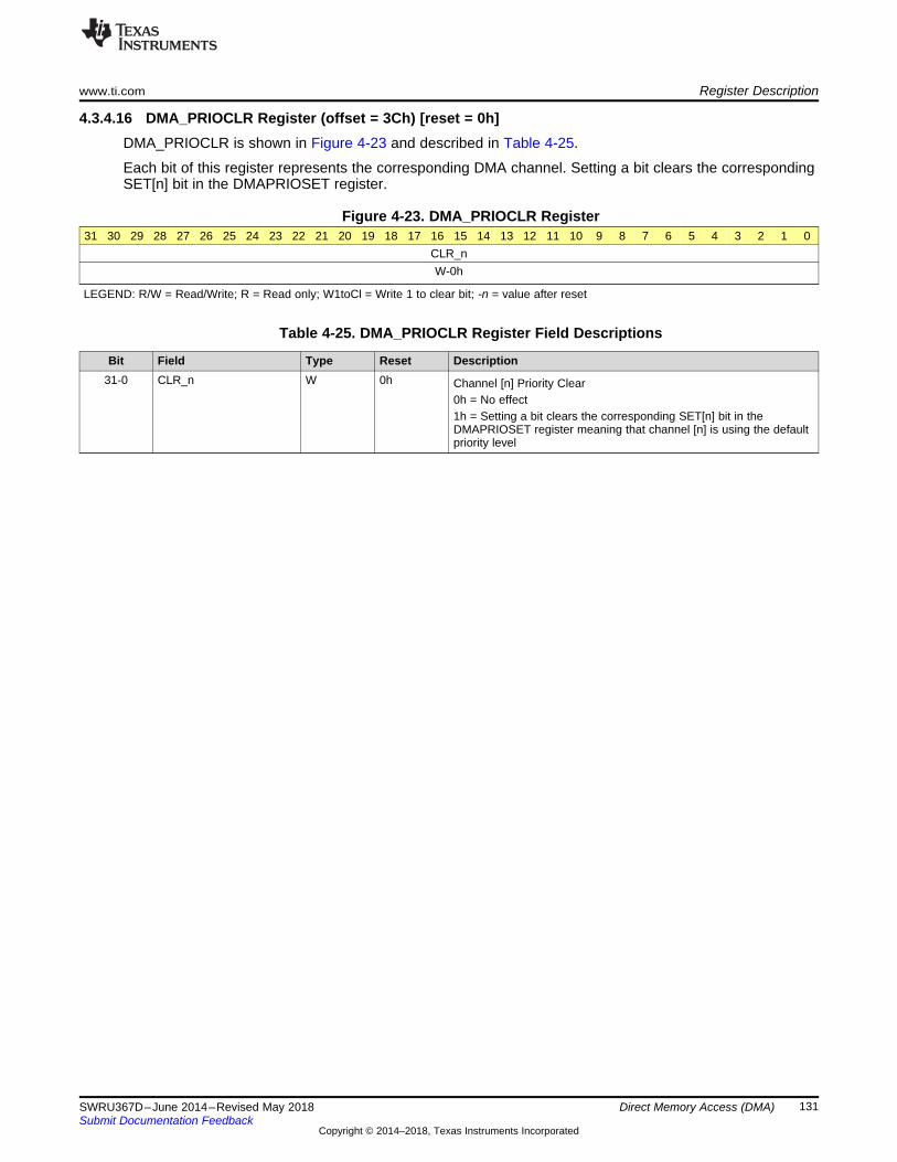
www.ti.com Register Description
131SWRU367D–June 2014–Revised May 2018Submit Documentation Feedback
Copyright © 2014–2018, Texas Instruments Incorporated
Direct Memory Access (DMA)
4.3.4.16 DMA_PRIOCLR Register (offset = 3Ch) [reset = 0h]DMA_PRIOCLR is shown in Figure 4-23 and described in Table 4-25.
Each bit of this register represents the corresponding DMA channel. Setting a bit clears the correspondingSET[n] bit in the DMAPRIOSET register.
Figure 4-23. DMA_PRIOCLR Register31 30 29 28 27 26 25 24 23 22 21 20 19 18 17 16 15 14 13 12 11 10 9 8 7 6 5 4 3 2 1 0
CLR_nW-0h
LEGEND: R/W = Read/Write; R = Read only; W1toCl = Write 1 to clear bit; -n = value after reset
Table 4-25. DMA_PRIOCLR Register Field Descriptions
Bit Field Type Reset Description31-0 CLR_n W 0h Channel [n] Priority Clear
0h = No effect1h = Setting a bit clears the corresponding SET[n] bit in theDMAPRIOSET register meaning that channel [n] is using the defaultpriority level
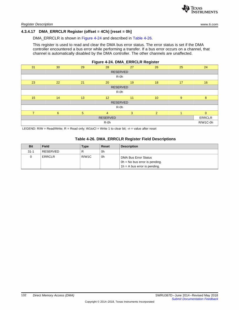
Register Description www.ti.com
132 SWRU367D–June 2014–Revised May 2018Submit Documentation Feedback
Copyright © 2014–2018, Texas Instruments Incorporated
Direct Memory Access (DMA)
4.3.4.17 DMA_ERRCLR Register (offset = 4Ch) [reset = 0h]DMA_ERRCLR is shown in Figure 4-24 and described in Table 4-26.
This register is used to read and clear the DMA bus error status. The error status is set if the DMAcontroller encountered a bus error while performing a transfer. If a bus error occurs on a channel, thatchannel is automatically disabled by the DMA controller. The other channels are unaffected.
Figure 4-24. DMA_ERRCLR Register31 30 29 28 27 26 25 24
RESERVEDR-0h
23 22 21 20 19 18 17 16RESERVED
R-0h
15 14 13 12 11 10 9 8RESERVED
R-0h
7 6 5 4 3 2 1 0RESERVED ERRCLR
R-0h R/W1C-0h
LEGEND: R/W = Read/Write; R = Read only; W1toCl = Write 1 to clear bit; -n = value after reset
Table 4-26. DMA_ERRCLR Register Field Descriptions
Bit Field Type Reset Description31-1 RESERVED R 0h
0 ERRCLR R/W1C 0h DMA Bus Error Status0h = No bus error is pending.1h = A bus error is pending.
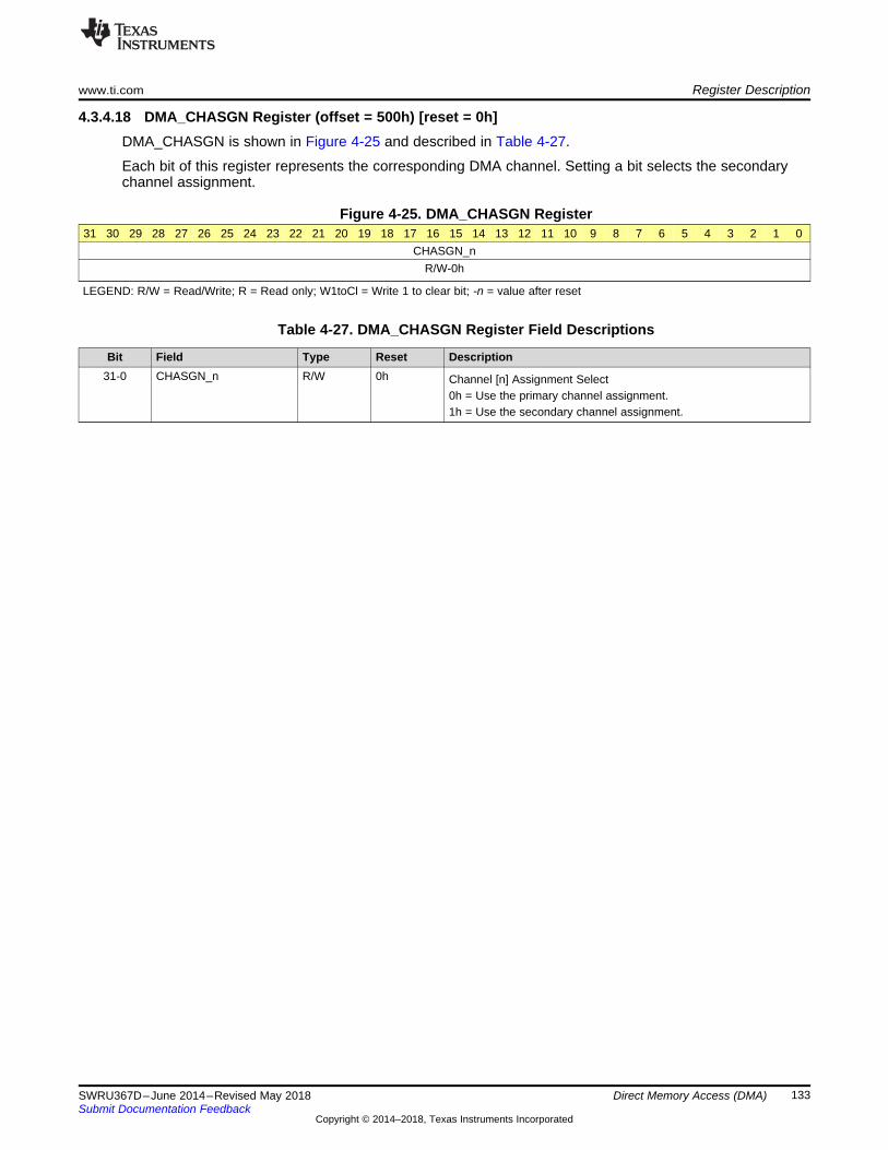
www.ti.com Register Description
133SWRU367D–June 2014–Revised May 2018Submit Documentation Feedback
Copyright © 2014–2018, Texas Instruments Incorporated
Direct Memory Access (DMA)
4.3.4.18 DMA_CHASGN Register (offset = 500h) [reset = 0h]DMA_CHASGN is shown in Figure 4-25 and described in Table 4-27.
Each bit of this register represents the corresponding DMA channel. Setting a bit selects the secondarychannel assignment.
Figure 4-25. DMA_CHASGN Register31 30 29 28 27 26 25 24 23 22 21 20 19 18 17 16 15 14 13 12 11 10 9 8 7 6 5 4 3 2 1 0
CHASGN_nR/W-0h
LEGEND: R/W = Read/Write; R = Read only; W1toCl = Write 1 to clear bit; -n = value after reset
Table 4-27. DMA_CHASGN Register Field Descriptions
Bit Field Type Reset Description31-0 CHASGN_n R/W 0h Channel [n] Assignment Select
0h = Use the primary channel assignment.1h = Use the secondary channel assignment.

Register Description www.ti.com
134 SWRU367D–June 2014–Revised May 2018Submit Documentation Feedback
Copyright © 2014–2018, Texas Instruments Incorporated
Direct Memory Access (DMA)
4.3.4.19 DMA_CHMAP0 Register (offset = 510h) [reset = 0h]DMA_CHMAP0 is shown in Figure 4-26 and described in Table 4-28.
Each 4-bit field of the DMACHMAP0 register configures the DMA channel assignment.
Figure 4-26. DMA_CHMAP0 Register31 30 29 28 27 26 25 24 23 22 21 20 19 18 17 16
CH7SEL_n CH6SEL_n CH5SEL_n CH4SEL_nR/W-0h R/W-0h R/W-0h R/W-0h
15 14 13 12 11 10 9 8 7 6 5 4 3 2 1 0CH3SEL_n CH2SEL_n CH1SEL_n CH0SEL_n
R/W-0h R/W-0h R/W-0h R/W-0h
LEGEND: R/W = Read/Write; R = Read only; W1toCl = Write 1 to clear bit; -n = value after reset
Table 4-28. DMA_CHMAP0 Register Field Descriptions
Bit Field Type Reset Description31-28 CH7SEL_n R/W 0h DMA channel 7 source select27-24 CH6SEL_n R/W 0h DMA channel 6 source select23-20 CH5SEL_n R/W 0h DMA channel 5 source select19-16 CH4SEL_n R/W 0h DMA channel 4 source select15-12 CH3SEL_n R/W 0h DMA channel 3 source select11-8 CH2SEL_n R/W 0h DMA channel 2 source select7-4 CH1SEL_n R/W 0h DMA channel 1 source select3-0 CH0SEL_n R/W 0h DMA channel 0 source select
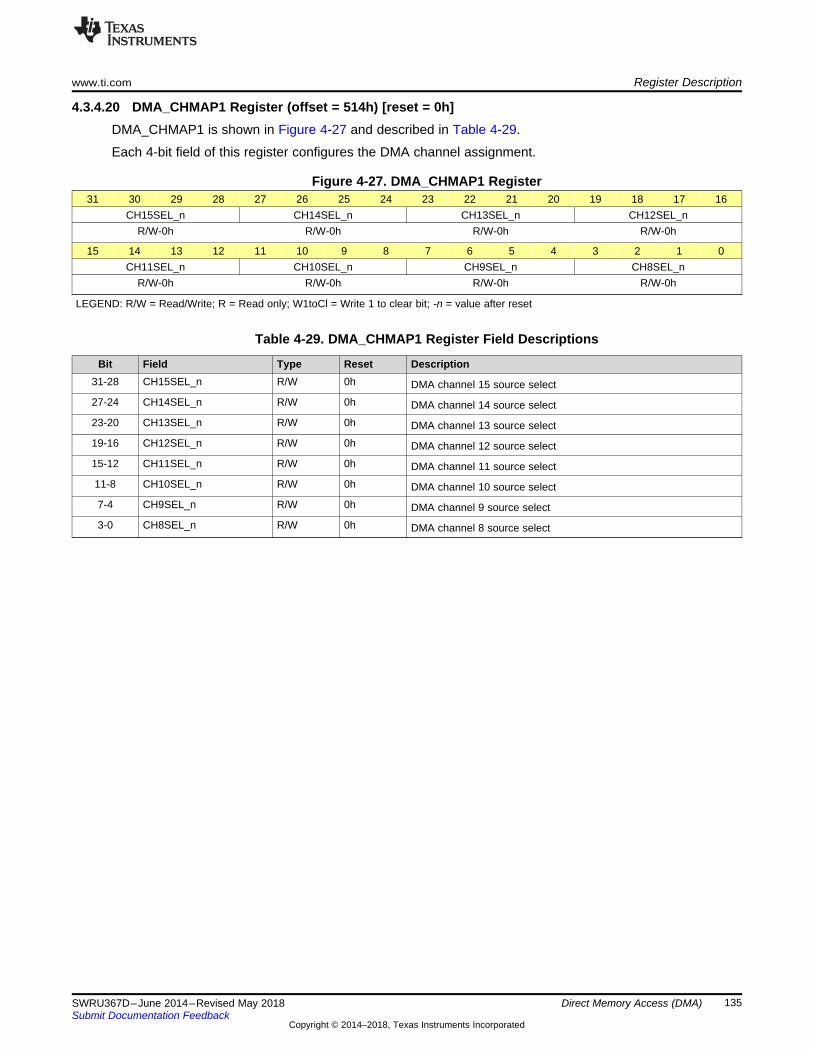
www.ti.com Register Description
135SWRU367D–June 2014–Revised May 2018Submit Documentation Feedback
Copyright © 2014–2018, Texas Instruments Incorporated
Direct Memory Access (DMA)
4.3.4.20 DMA_CHMAP1 Register (offset = 514h) [reset = 0h]DMA_CHMAP1 is shown in Figure 4-27 and described in Table 4-29.
Each 4-bit field of this register configures the DMA channel assignment.
Figure 4-27. DMA_CHMAP1 Register31 30 29 28 27 26 25 24 23 22 21 20 19 18 17 16
CH15SEL_n CH14SEL_n CH13SEL_n CH12SEL_nR/W-0h R/W-0h R/W-0h R/W-0h
15 14 13 12 11 10 9 8 7 6 5 4 3 2 1 0CH11SEL_n CH10SEL_n CH9SEL_n CH8SEL_n
R/W-0h R/W-0h R/W-0h R/W-0h
LEGEND: R/W = Read/Write; R = Read only; W1toCl = Write 1 to clear bit; -n = value after reset
Table 4-29. DMA_CHMAP1 Register Field Descriptions
Bit Field Type Reset Description31-28 CH15SEL_n R/W 0h DMA channel 15 source select27-24 CH14SEL_n R/W 0h DMA channel 14 source select23-20 CH13SEL_n R/W 0h DMA channel 13 source select19-16 CH12SEL_n R/W 0h DMA channel 12 source select15-12 CH11SEL_n R/W 0h DMA channel 11 source select11-8 CH10SEL_n R/W 0h DMA channel 10 source select7-4 CH9SEL_n R/W 0h DMA channel 9 source select3-0 CH8SEL_n R/W 0h DMA channel 8 source select

Register Description www.ti.com
136 SWRU367D–June 2014–Revised May 2018Submit Documentation Feedback
Copyright © 2014–2018, Texas Instruments Incorporated
Direct Memory Access (DMA)
4.3.4.21 DMA_CHMAP2 Register (offset = 518h) [reset = 0h]DMA_CHMAP2 is shown in Figure 4-28 and described in Table 4-30.
Each 4-bit field of this register configures the DMA channel assignment.
Figure 4-28. DMA_CHMAP2 Register31 30 29 28 27 26 25 24 23 22 21 20 19 18 17 16
CH23SEL_n CH22SEL_n CH21SEL_n CH20SEL_nR/W-0h R/W-0h R/W-0h R/W-0h
15 14 13 12 11 10 9 8 7 6 5 4 3 2 1 0CH19SEL_n CH18SEL_n CH17SEL_n CH16SEL_n
R/W-0h R/W-0h R/W-0h R/W-0h
LEGEND: R/W = Read/Write; R = Read only; W1toCl = Write 1 to clear bit; -n = value after reset
Table 4-30. DMA_CHMAP2 Register Field Descriptions
Bit Field Type Reset Description31-28 CH23SEL_n R/W 0h DMA channel 23 source select27-24 CH22SEL_n R/W 0h DMA channel 22 source select23-20 CH21SEL_n R/W 0h DMA channel 21 source select19-16 CH20SEL_n R/W 0h DMA channel 20 source select15-12 CH19SEL_n R/W 0h DMA channel 19 source select11-8 CH18SEL_n R/W 0h DMA channel 18 source select7-4 CH17SEL_n R/W 0h DMA channel 17 source select3-0 CH16SEL_n R/W 0h DMA channel 16 source select

www.ti.com Register Description
137SWRU367D–June 2014–Revised May 2018Submit Documentation Feedback
Copyright © 2014–2018, Texas Instruments Incorporated
Direct Memory Access (DMA)
4.3.4.22 DMA_CHMAP3 Register (offset = 51Ch) [reset = 0h]DMA_CHMAP3 is shown in Figure 4-29 and described in Table 4-31.
Each 4-bit field of this register configures the DMA channel assignment.
Figure 4-29. DMA_CHMAP3 Register31 30 29 28 27 26 25 24 23 22 21 20 19 18 17 16
CH31SEL_n CH30SEL_n CH29SEL_n CH28SEL_nR/W-0h R/W-0h R/W-0h R/W-0h
15 14 13 12 11 10 9 8 7 6 5 4 3 2 1 0CH27SEL_n CH26SEL_n CH25SEL_n CH24SEL_n
R/W-0h R/W-0h R/W-0h R/W-0h
LEGEND: R/W = Read/Write; R = Read only; W1toCl = Write 1 to clear bit; -n = value after reset
Table 4-31. DMA_CHMAP3 Register Field Descriptions
Bit Field Type Reset Description31-28 CH31SEL_n R/W 0h DMA channel 31 source select27-24 CH30SEL_n R/W 0h DMA channel 30 source select23-20 CH29SEL_n R/W 0h DMA channel 29 source select19-16 CH28SEL_n R/W 0h DMA channel 28 source select15-12 CH27SEL_n R/W 0h DMA channel 27 source select11-8 CH26SEL_n R/W 0h DMA channel 26 source select7-4 CH25SEL_n R/W 0h DMA channel 25 source select3-0 CH24SEL_n R/W 0h DMA channel 24 source select
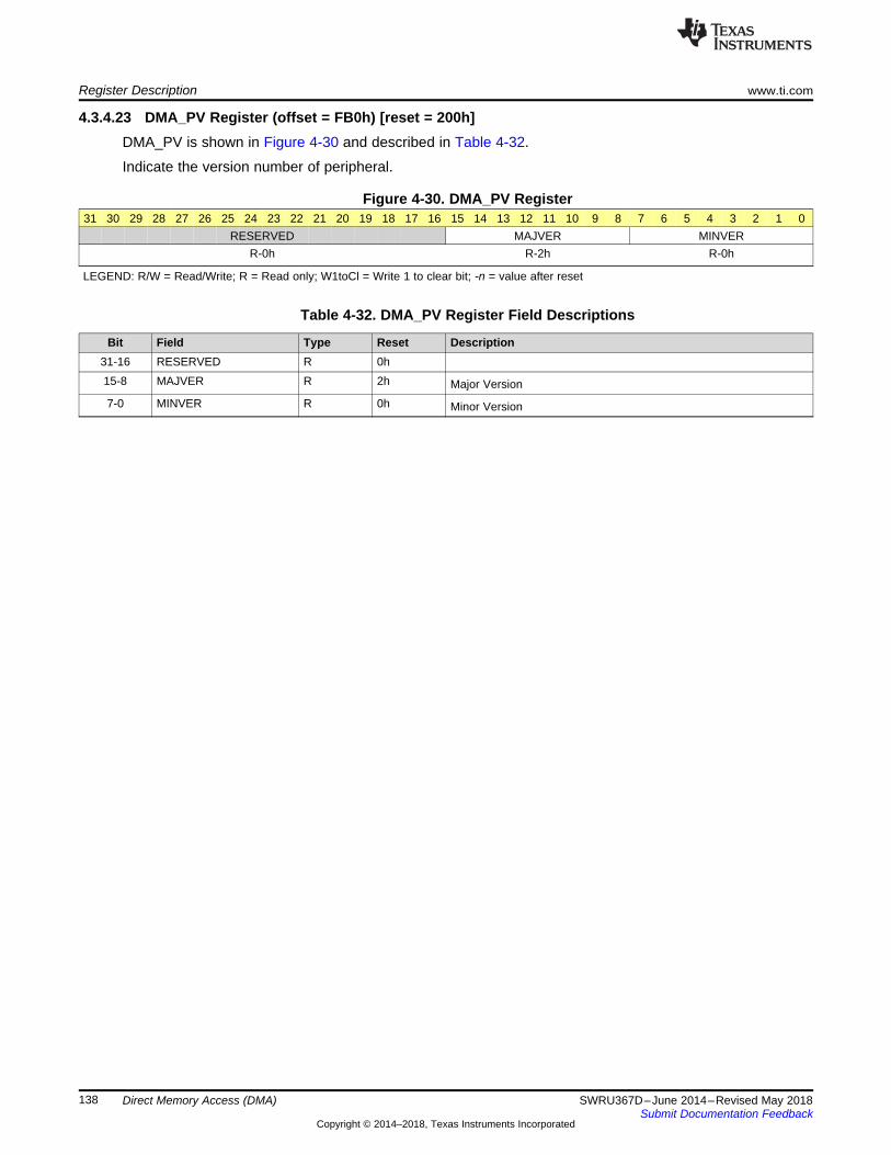
Register Description www.ti.com
138 SWRU367D–June 2014–Revised May 2018Submit Documentation Feedback
Copyright © 2014–2018, Texas Instruments Incorporated
Direct Memory Access (DMA)
4.3.4.23 DMA_PV Register (offset = FB0h) [reset = 200h]DMA_PV is shown in Figure 4-30 and described in Table 4-32.
Indicate the version number of peripheral.
Figure 4-30. DMA_PV Register31 30 29 28 27 26 25 24 23 22 21 20 19 18 17 16 15 14 13 12 11 10 9 8 7 6 5 4 3 2 1 0
RESERVED MAJVER MINVERR-0h R-2h R-0h
LEGEND: R/W = Read/Write; R = Read only; W1toCl = Write 1 to clear bit; -n = value after reset
Table 4-32. DMA_PV Register Field Descriptions
Bit Field Type Reset Description31-16 RESERVED R 0h15-8 MAJVER R 2h Major Version7-0 MINVER R 0h Minor Version
139SWRU367D–June 2014–Revised May 2018Submit Documentation Feedback
Copyright © 2014–2018, Texas Instruments Incorporated
General-Purpose Input/Outputs (GPIOs)
Chapter 5SWRU367D–June 2014–Revised May 2018
General-Purpose Input/Outputs (GPIOs)
Topic ........................................................................................................................... Page
5.1 Overview ......................................................................................................... 1405.2 Functional Description ...................................................................................... 1405.3 Interrupt Control............................................................................................... 1425.4 Initialization and Configuration .......................................................................... 1425.5 GPIO_REGISTER_MAP Registers ....................................................................... 144
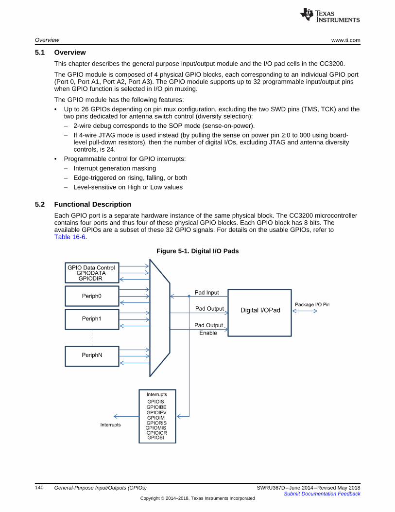
Overview www.ti.com
140 SWRU367D–June 2014–Revised May 2018Submit Documentation Feedback
Copyright © 2014–2018, Texas Instruments Incorporated
General-Purpose Input/Outputs (GPIOs)
5.1 OverviewThis chapter describes the general purpose input/output module and the I/O pad cells in the CC3200.
The GPIO module is composed of 4 physical GPIO blocks, each corresponding to an individual GPIO port(Port 0, Port A1, Port A2, Port A3). The GPIO module supports up to 32 programmable input/output pinswhen GPIO function is selected in I/O pin muxing.
The GPIO module has the following features:• Up to 26 GPIOs depending on pin mux configuration, excluding the two SWD pins (TMS, TCK) and the
two pins dedicated for antenna switch control (diversity selection):– 2-wire debug corresponds to the SOP mode (sense-on-power).– If 4-wire JTAG mode is used instead (by pulling the sense on power pin 2:0 to 000 using board-
level pull-down resistors), then the number of digital I/Os, excluding JTAG and antenna diversitycontrols, is 24.
• Programmable control for GPIO interrupts:– Interrupt generation masking– Edge-triggered on rising, falling, or both– Level-sensitive on High or Low values
5.2 Functional DescriptionEach GPIO port is a separate hardware instance of the same physical block. The CC3200 microcontrollercontains four ports and thus four of these physical GPIO blocks. Each GPIO block has 8 bits. Theavailable GPIOs are a subset of these 32 GPIO signals. For details on the usable GPIOs, refer toTable 16-6.
Figure 5-1. Digital I/O Pads
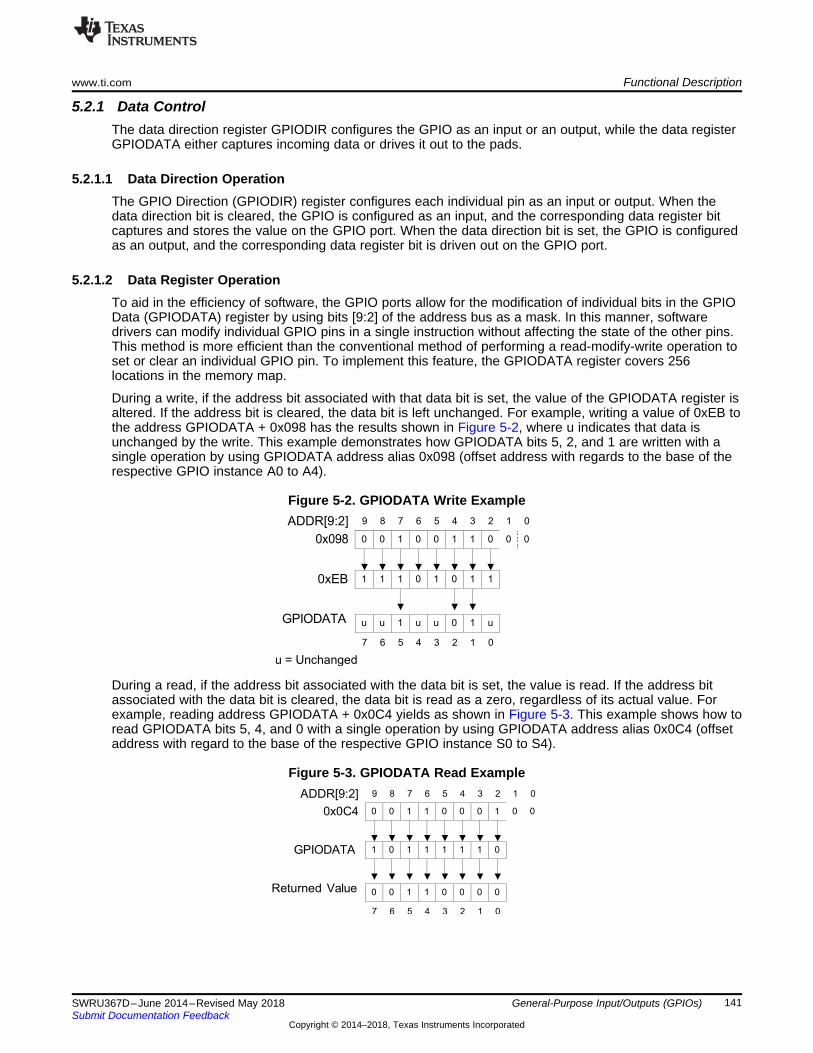
www.ti.com Functional Description
141SWRU367D–June 2014–Revised May 2018Submit Documentation Feedback
Copyright © 2014–2018, Texas Instruments Incorporated
General-Purpose Input/Outputs (GPIOs)
5.2.1 Data ControlThe data direction register GPIODIR configures the GPIO as an input or an output, while the data registerGPIODATA either captures incoming data or drives it out to the pads.
5.2.1.1 Data Direction OperationThe GPIO Direction (GPIODIR) register configures each individual pin as an input or output. When thedata direction bit is cleared, the GPIO is configured as an input, and the corresponding data register bitcaptures and stores the value on the GPIO port. When the data direction bit is set, the GPIO is configuredas an output, and the corresponding data register bit is driven out on the GPIO port.
5.2.1.2 Data Register OperationTo aid in the efficiency of software, the GPIO ports allow for the modification of individual bits in the GPIOData (GPIODATA) register by using bits [9:2] of the address bus as a mask. In this manner, softwaredrivers can modify individual GPIO pins in a single instruction without affecting the state of the other pins.This method is more efficient than the conventional method of performing a read-modify-write operation toset or clear an individual GPIO pin. To implement this feature, the GPIODATA register covers 256locations in the memory map.
During a write, if the address bit associated with that data bit is set, the value of the GPIODATA register isaltered. If the address bit is cleared, the data bit is left unchanged. For example, writing a value of 0xEB tothe address GPIODATA + 0x098 has the results shown in Figure 5-2, where u indicates that data isunchanged by the write. This example demonstrates how GPIODATA bits 5, 2, and 1 are written with asingle operation by using GPIODATA address alias 0x098 (offset address with regards to the base of therespective GPIO instance A0 to A4).
Figure 5-2. GPIODATA Write Example
During a read, if the address bit associated with the data bit is set, the value is read. If the address bitassociated with the data bit is cleared, the data bit is read as a zero, regardless of its actual value. Forexample, reading address GPIODATA + 0x0C4 yields as shown in Figure 5-3. This example shows how toread GPIODATA bits 5, 4, and 0 with a single operation by using GPIODATA address alias 0x0C4 (offsetaddress with regard to the base of the respective GPIO instance S0 to S4).
Figure 5-3. GPIODATA Read Example
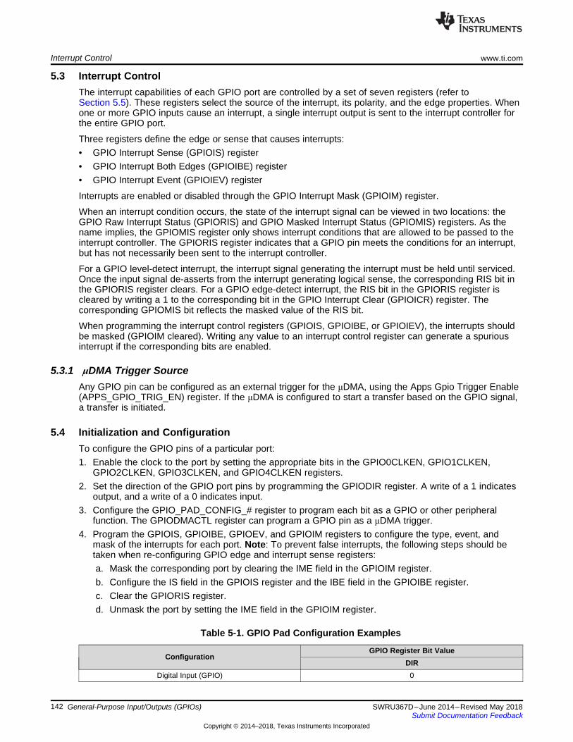
Interrupt Control www.ti.com
142 SWRU367D–June 2014–Revised May 2018Submit Documentation Feedback
Copyright © 2014–2018, Texas Instruments Incorporated
General-Purpose Input/Outputs (GPIOs)
5.3 Interrupt ControlThe interrupt capabilities of each GPIO port are controlled by a set of seven registers (refer toSection 5.5). These registers select the source of the interrupt, its polarity, and the edge properties. Whenone or more GPIO inputs cause an interrupt, a single interrupt output is sent to the interrupt controller forthe entire GPIO port.
Three registers define the edge or sense that causes interrupts:• GPIO Interrupt Sense (GPIOIS) register• GPIO Interrupt Both Edges (GPIOIBE) register• GPIO Interrupt Event (GPIOIEV) register
Interrupts are enabled or disabled through the GPIO Interrupt Mask (GPIOIM) register.
When an interrupt condition occurs, the state of the interrupt signal can be viewed in two locations: theGPIO Raw Interrupt Status (GPIORIS) and GPIO Masked Interrupt Status (GPIOMIS) registers. As thename implies, the GPIOMIS register only shows interrupt conditions that are allowed to be passed to theinterrupt controller. The GPIORIS register indicates that a GPIO pin meets the conditions for an interrupt,but has not necessarily been sent to the interrupt controller.
For a GPIO level-detect interrupt, the interrupt signal generating the interrupt must be held until serviced.Once the input signal de-asserts from the interrupt generating logical sense, the corresponding RIS bit inthe GPIORIS register clears. For a GPIO edge-detect interrupt, the RIS bit in the GPIORIS register iscleared by writing a 1 to the corresponding bit in the GPIO Interrupt Clear (GPIOICR) register. Thecorresponding GPIOMIS bit reflects the masked value of the RIS bit.
When programming the interrupt control registers (GPIOIS, GPIOIBE, or GPIOIEV), the interrupts shouldbe masked (GPIOIM cleared). Writing any value to an interrupt control register can generate a spuriousinterrupt if the corresponding bits are enabled.
5.3.1 μDMA Trigger SourceAny GPIO pin can be configured as an external trigger for the μDMA, using the Apps Gpio Trigger Enable(APPS_GPIO_TRIG_EN) register. If the μDMA is configured to start a transfer based on the GPIO signal,a transfer is initiated.
5.4 Initialization and ConfigurationTo configure the GPIO pins of a particular port:1. Enable the clock to the port by setting the appropriate bits in the GPIO0CLKEN, GPIO1CLKEN,
GPIO2CLKEN, GPIO3CLKEN, and GPIO4CLKEN registers.2. Set the direction of the GPIO port pins by programming the GPIODIR register. A write of a 1 indicates
output, and a write of a 0 indicates input.3. Configure the GPIO_PAD_CONFIG_# register to program each bit as a GPIO or other peripheral
function. The GPIODMACTL register can program a GPIO pin as a μDMA trigger.4. Program the GPIOIS, GPIOIBE, GPIOEV, and GPIOIM registers to configure the type, event, and
mask of the interrupts for each port. Note: To prevent false interrupts, the following steps should betaken when re-configuring GPIO edge and interrupt sense registers:a. Mask the corresponding port by clearing the IME field in the GPIOIM register.b. Configure the IS field in the GPIOIS register and the IBE field in the GPIOIBE register.c. Clear the GPIORIS register.d. Unmask the port by setting the IME field in the GPIOIM register.
Table 5-1. GPIO Pad Configuration Examples
ConfigurationGPIO Register Bit Value
DIRDigital Input (GPIO) 0
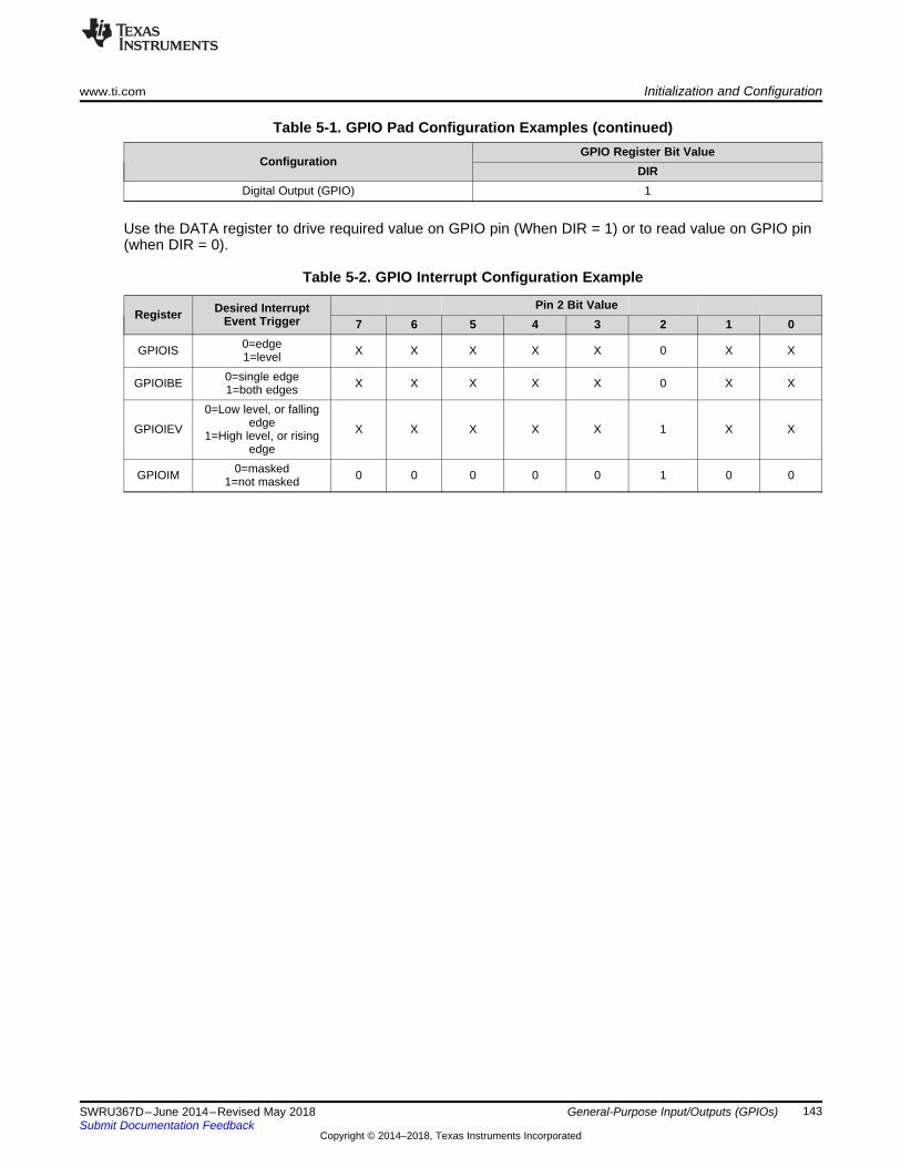
www.ti.com Initialization and Configuration
143SWRU367D–June 2014–Revised May 2018Submit Documentation Feedback
Copyright © 2014–2018, Texas Instruments Incorporated
General-Purpose Input/Outputs (GPIOs)
Table 5-1. GPIO Pad Configuration Examples (continued)
ConfigurationGPIO Register Bit Value
DIRDigital Output (GPIO) 1
Use the DATA register to drive required value on GPIO pin (When DIR = 1) or to read value on GPIO pin(when DIR = 0).
Table 5-2. GPIO Interrupt Configuration Example
Register Desired InterruptEvent Trigger
Pin 2 Bit Value7 6 5 4 3 2 1 0
GPIOIS 0=edge1=level X X X X X 0 X X
GPIOIBE 0=single edge1=both edges X X X X X 0 X X
GPIOIEV
0=Low level, or fallingedge
1=High level, or risingedge
X X X X X 1 X X
GPIOIM 0=masked1=not masked 0 0 0 0 0 1 0 0
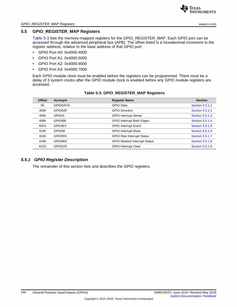
GPIO_REGISTER_MAP Registers www.ti.com
144 SWRU367D–June 2014–Revised May 2018Submit Documentation Feedback
Copyright © 2014–2018, Texas Instruments Incorporated
General-Purpose Input/Outputs (GPIOs)
5.5 GPIO_REGISTER_MAP RegistersTable 5-3 lists the memory-mapped registers for the GPIO_REGISTER_MAP. Each GPIO port can beaccessed through the advanced peripheral bus (APB). The offset listed is a hexadecimal increment to theregister address, relative to the base address of that GPIO port:• GPIO Port A0: 0x4000.4000• GPIO Port A1: 0x4000.5000• GPIO Port A2: 0x4000.6000• GPIO Port A3: 0x4000.7000
Each GPIO module clock must be enabled before the registers can be programmed. There must be adelay of 3 system clocks after the GPIO module clock is enabled before any GPIO module registers areaccessed.
Table 5-3. GPIO_REGISTER_MAP Registers
Offset Acronym Register Name Section0h GPIODATA GPIO Data Section 5.5.1.1
400h GPIODIR GPIO Direction Section 5.5.1.2404h GPIOIS GPIO Interrupt Sense Section 5.5.1.3408h GPIOIBE GPIO Interrupt Both Edges Section 5.5.1.440Ch GPIOIEV GPIO Interrupt Event Section 5.5.1.5410h GPIOIM GPIO Interrupt Mask Section 5.5.1.6414h GPIORIS GPIO Raw Interrupt Status Section 5.5.1.7418h GPIOMIS GPIO Masked Interrupt Status Section 5.5.1.841Ch GPIOICR GPIO Interrupt Clear Section 5.5.1.9
5.5.1 GPIO Register DescriptionThe remainder of this section lists and describes the GPIO registers.

www.ti.com GPIO_REGISTER_MAP Registers
145SWRU367D–June 2014–Revised May 2018Submit Documentation Feedback
Copyright © 2014–2018, Texas Instruments Incorporated
General-Purpose Input/Outputs (GPIOs)
5.5.1.1 GPIODATA Register (offset = 0h) [reset = 0h]GPIODATA is shown in Figure 5-4 and described in Table 5-4.
The GPIODATA register is the data register. In software control mode, values written in the GPIODATAregister are transferred onto the GPIO port pins if the respective pins have been configured as outputsthrough the GPIO Direction (GPIODIR) register.The GPIODATA register has 256 aliased addresses from offset 0x000 to 0x3FF. A different address aliasis used to directly read/ or write any combination of the 8 signal bits. This feature can help avoid time-consuming read-modify-writes and bit-masking operation for read-in software.In this scheme, to write to GPIODATA, the corresponding bits in the mask, represented by the addressbus bits [9:2], must be set. Otherwise, the bit values remain unchanged by the write.Similarly, the values read from this register are determined for each bit by the mask bit derived from thealias address used to access the data register, bits [9:2]. Bits set in the address mask cause thecorresponding bits in GPIODATA to be read, and bits that are clear in the address mask cause thecorresponding bits in GPIODATA to be read as 0, regardless of their value.A read from GPIODATA returns the last bit value written if the respective pins are configured as outputs,or it returns the value on the corresponding input pin when these are configured as inputs. All bits arecleared by a reset.
Figure 5-4. GPIODATA Register31 30 29 28 27 26 25 24 23 22 21 20 19 18 17 16 15 14 13 12 11 10 9 8 7 6 5 4 3 2 1 0
RESERVED DATAR-0h R/W-0h
Table 5-4. GPIODATA Register Field Descriptions
Bit Field Type Reset Description31-8 RESERVED R 0h Software should not rely on the value of a reserved bit. To provide
compatibility with future products, the value of a reserved bit shouldbe preserved across a read-modify-write operation.
7-0 DATA R/W 0h GPIO DataThis register is virtually mapped to 256 locations in the addressspace. To facilitate the reading and writing of data to these registersby independent drivers, the data read from and written to theregisters are masked by the eight address lines [9:2]. Reads fromthis register return its current state. Writes to this register only affectbits that are not masked by ADDR[9:2] and are configured asoutputs.
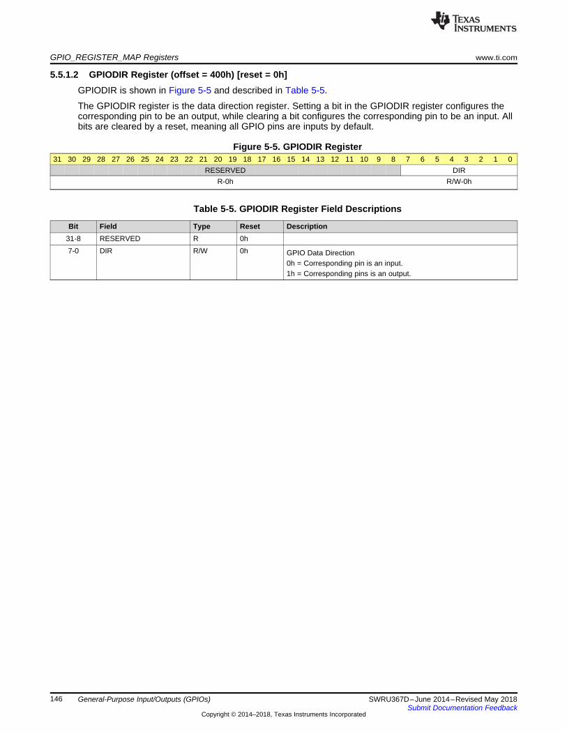
GPIO_REGISTER_MAP Registers www.ti.com
146 SWRU367D–June 2014–Revised May 2018Submit Documentation Feedback
Copyright © 2014–2018, Texas Instruments Incorporated
General-Purpose Input/Outputs (GPIOs)
5.5.1.2 GPIODIR Register (offset = 400h) [reset = 0h]GPIODIR is shown in Figure 5-5 and described in Table 5-5.
The GPIODIR register is the data direction register. Setting a bit in the GPIODIR register configures thecorresponding pin to be an output, while clearing a bit configures the corresponding pin to be an input. Allbits are cleared by a reset, meaning all GPIO pins are inputs by default.
Figure 5-5. GPIODIR Register31 30 29 28 27 26 25 24 23 22 21 20 19 18 17 16 15 14 13 12 11 10 9 8 7 6 5 4 3 2 1 0
RESERVED DIRR-0h R/W-0h
Table 5-5. GPIODIR Register Field Descriptions
Bit Field Type Reset Description31-8 RESERVED R 0h7-0 DIR R/W 0h GPIO Data Direction
0h = Corresponding pin is an input.1h = Corresponding pins is an output.
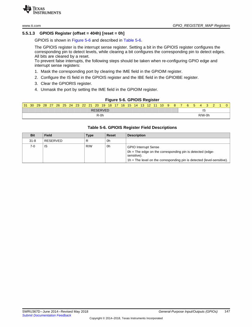
www.ti.com GPIO_REGISTER_MAP Registers
147SWRU367D–June 2014–Revised May 2018Submit Documentation Feedback
Copyright © 2014–2018, Texas Instruments Incorporated
General-Purpose Input/Outputs (GPIOs)
5.5.1.3 GPIOIS Register (offset = 404h) [reset = 0h]GPIOIS is shown in Figure 5-6 and described in Table 5-6.
The GPIOIS register is the interrupt sense register. Setting a bit in the GPIOIS register configures thecorresponding pin to detect levels, while clearing a bit configures the corresponding pin to detect edges.All bits are cleared by a reset.To prevent false interrupts, the following steps should be taken when re-configuring GPIO edge andinterrupt sense registers:1. Mask the corresponding port by clearing the IME field in the GPIOIM register.2. Configure the IS field in the GPIOIS register and the IBE field in the GPIOIBE register.3. Clear the GPIORIS register.4. Unmask the port by setting the IME field in the GPIOIM register.
Figure 5-6. GPIOIS Register31 30 29 28 27 26 25 24 23 22 21 20 19 18 17 16 15 14 13 12 11 10 9 8 7 6 5 4 3 2 1 0
RESERVED ISR-0h R/W-0h
Table 5-6. GPIOIS Register Field Descriptions
Bit Field Type Reset Description31-8 RESERVED R 0h7-0 IS R/W 0h GPIO Interrupt Sense
0h = The edge on the corresponding pin is detected (edge-sensitive).1h = The level on the corresponding pin is detected (level-sensitive).
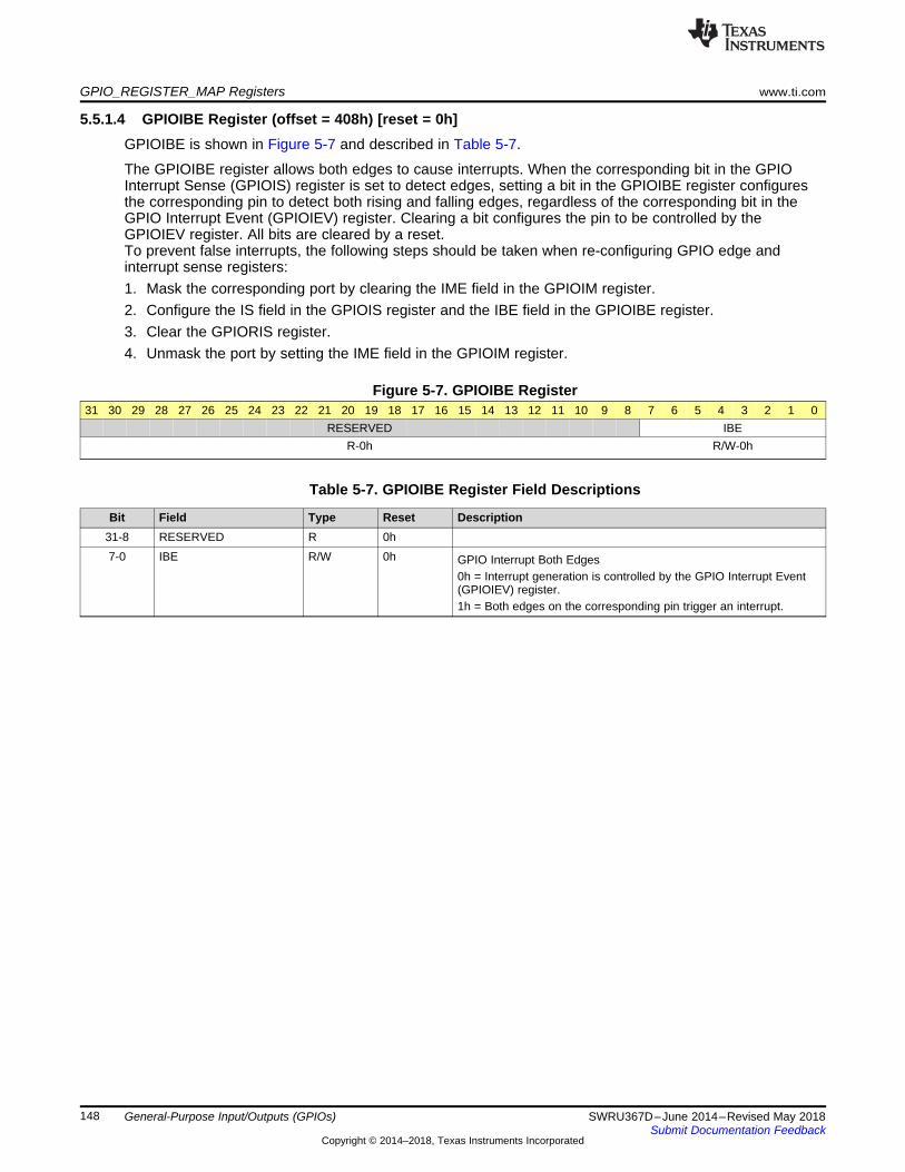
GPIO_REGISTER_MAP Registers www.ti.com
148 SWRU367D–June 2014–Revised May 2018Submit Documentation Feedback
Copyright © 2014–2018, Texas Instruments Incorporated
General-Purpose Input/Outputs (GPIOs)
5.5.1.4 GPIOIBE Register (offset = 408h) [reset = 0h]GPIOIBE is shown in Figure 5-7 and described in Table 5-7.
The GPIOIBE register allows both edges to cause interrupts. When the corresponding bit in the GPIOInterrupt Sense (GPIOIS) register is set to detect edges, setting a bit in the GPIOIBE register configuresthe corresponding pin to detect both rising and falling edges, regardless of the corresponding bit in theGPIO Interrupt Event (GPIOIEV) register. Clearing a bit configures the pin to be controlled by theGPIOIEV register. All bits are cleared by a reset.To prevent false interrupts, the following steps should be taken when re-configuring GPIO edge andinterrupt sense registers:1. Mask the corresponding port by clearing the IME field in the GPIOIM register.2. Configure the IS field in the GPIOIS register and the IBE field in the GPIOIBE register.3. Clear the GPIORIS register.4. Unmask the port by setting the IME field in the GPIOIM register.
Figure 5-7. GPIOIBE Register31 30 29 28 27 26 25 24 23 22 21 20 19 18 17 16 15 14 13 12 11 10 9 8 7 6 5 4 3 2 1 0
RESERVED IBER-0h R/W-0h
Table 5-7. GPIOIBE Register Field Descriptions
Bit Field Type Reset Description31-8 RESERVED R 0h7-0 IBE R/W 0h GPIO Interrupt Both Edges
0h = Interrupt generation is controlled by the GPIO Interrupt Event(GPIOIEV) register.1h = Both edges on the corresponding pin trigger an interrupt.
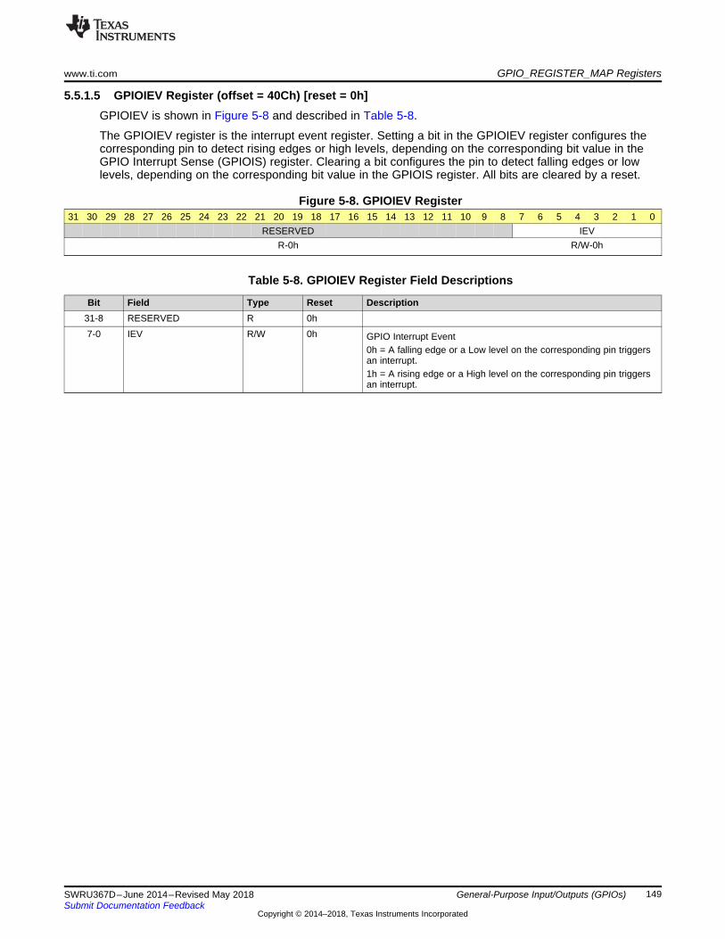
www.ti.com GPIO_REGISTER_MAP Registers
149SWRU367D–June 2014–Revised May 2018Submit Documentation Feedback
Copyright © 2014–2018, Texas Instruments Incorporated
General-Purpose Input/Outputs (GPIOs)
5.5.1.5 GPIOIEV Register (offset = 40Ch) [reset = 0h]GPIOIEV is shown in Figure 5-8 and described in Table 5-8.
The GPIOIEV register is the interrupt event register. Setting a bit in the GPIOIEV register configures thecorresponding pin to detect rising edges or high levels, depending on the corresponding bit value in theGPIO Interrupt Sense (GPIOIS) register. Clearing a bit configures the pin to detect falling edges or lowlevels, depending on the corresponding bit value in the GPIOIS register. All bits are cleared by a reset.
Figure 5-8. GPIOIEV Register31 30 29 28 27 26 25 24 23 22 21 20 19 18 17 16 15 14 13 12 11 10 9 8 7 6 5 4 3 2 1 0
RESERVED IEVR-0h R/W-0h
Table 5-8. GPIOIEV Register Field Descriptions
Bit Field Type Reset Description31-8 RESERVED R 0h7-0 IEV R/W 0h GPIO Interrupt Event
0h = A falling edge or a Low level on the corresponding pin triggersan interrupt.1h = A rising edge or a High level on the corresponding pin triggersan interrupt.
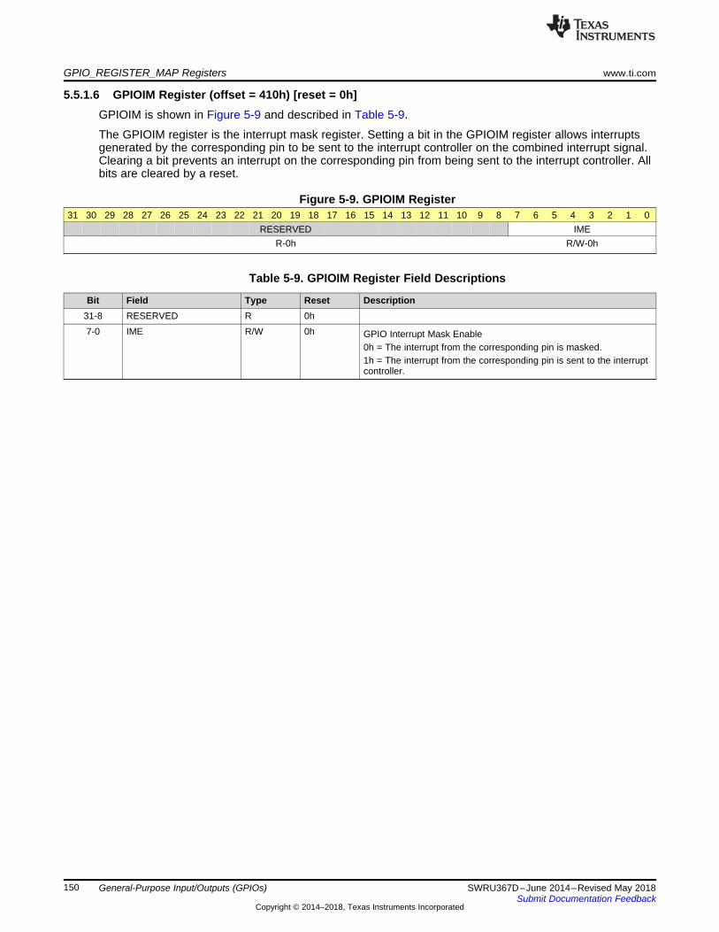
GPIO_REGISTER_MAP Registers www.ti.com
150 SWRU367D–June 2014–Revised May 2018Submit Documentation Feedback
Copyright © 2014–2018, Texas Instruments Incorporated
General-Purpose Input/Outputs (GPIOs)
5.5.1.6 GPIOIM Register (offset = 410h) [reset = 0h]GPIOIM is shown in Figure 5-9 and described in Table 5-9.
The GPIOIM register is the interrupt mask register. Setting a bit in the GPIOIM register allows interruptsgenerated by the corresponding pin to be sent to the interrupt controller on the combined interrupt signal.Clearing a bit prevents an interrupt on the corresponding pin from being sent to the interrupt controller. Allbits are cleared by a reset.
Figure 5-9. GPIOIM Register31 30 29 28 27 26 25 24 23 22 21 20 19 18 17 16 15 14 13 12 11 10 9 8 7 6 5 4 3 2 1 0
RESERVED IMER-0h R/W-0h
Table 5-9. GPIOIM Register Field Descriptions
Bit Field Type Reset Description31-8 RESERVED R 0h7-0 IME R/W 0h GPIO Interrupt Mask Enable
0h = The interrupt from the corresponding pin is masked.1h = The interrupt from the corresponding pin is sent to the interruptcontroller.
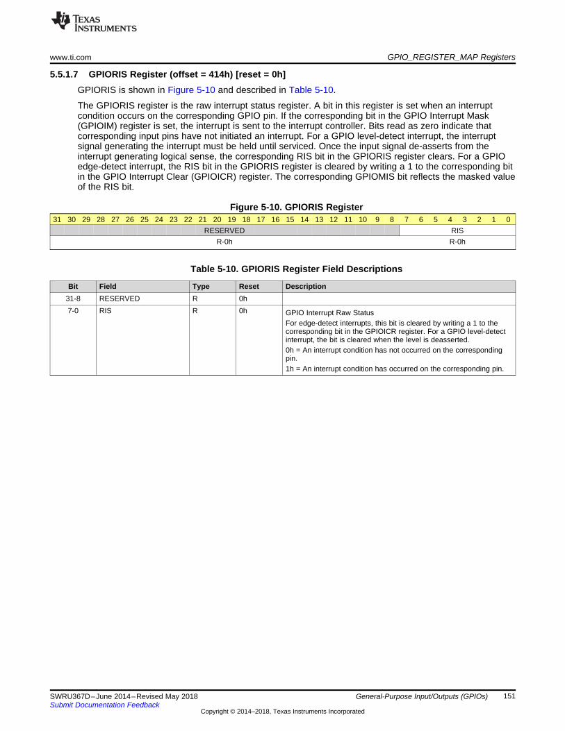
www.ti.com GPIO_REGISTER_MAP Registers
151SWRU367D–June 2014–Revised May 2018Submit Documentation Feedback
Copyright © 2014–2018, Texas Instruments Incorporated
General-Purpose Input/Outputs (GPIOs)
5.5.1.7 GPIORIS Register (offset = 414h) [reset = 0h]GPIORIS is shown in Figure 5-10 and described in Table 5-10.
The GPIORIS register is the raw interrupt status register. A bit in this register is set when an interruptcondition occurs on the corresponding GPIO pin. If the corresponding bit in the GPIO Interrupt Mask(GPIOIM) register is set, the interrupt is sent to the interrupt controller. Bits read as zero indicate thatcorresponding input pins have not initiated an interrupt. For a GPIO level-detect interrupt, the interruptsignal generating the interrupt must be held until serviced. Once the input signal de-asserts from theinterrupt generating logical sense, the corresponding RIS bit in the GPIORIS register clears. For a GPIOedge-detect interrupt, the RIS bit in the GPIORIS register is cleared by writing a 1 to the corresponding bitin the GPIO Interrupt Clear (GPIOICR) register. The corresponding GPIOMIS bit reflects the masked valueof the RIS bit.
Figure 5-10. GPIORIS Register31 30 29 28 27 26 25 24 23 22 21 20 19 18 17 16 15 14 13 12 11 10 9 8 7 6 5 4 3 2 1 0
RESERVED RISR-0h R-0h
Table 5-10. GPIORIS Register Field Descriptions
Bit Field Type Reset Description31-8 RESERVED R 0h7-0 RIS R 0h GPIO Interrupt Raw Status
For edge-detect interrupts, this bit is cleared by writing a 1 to thecorresponding bit in the GPIOICR register. For a GPIO level-detectinterrupt, the bit is cleared when the level is deasserted.0h = An interrupt condition has not occurred on the correspondingpin.1h = An interrupt condition has occurred on the corresponding pin.
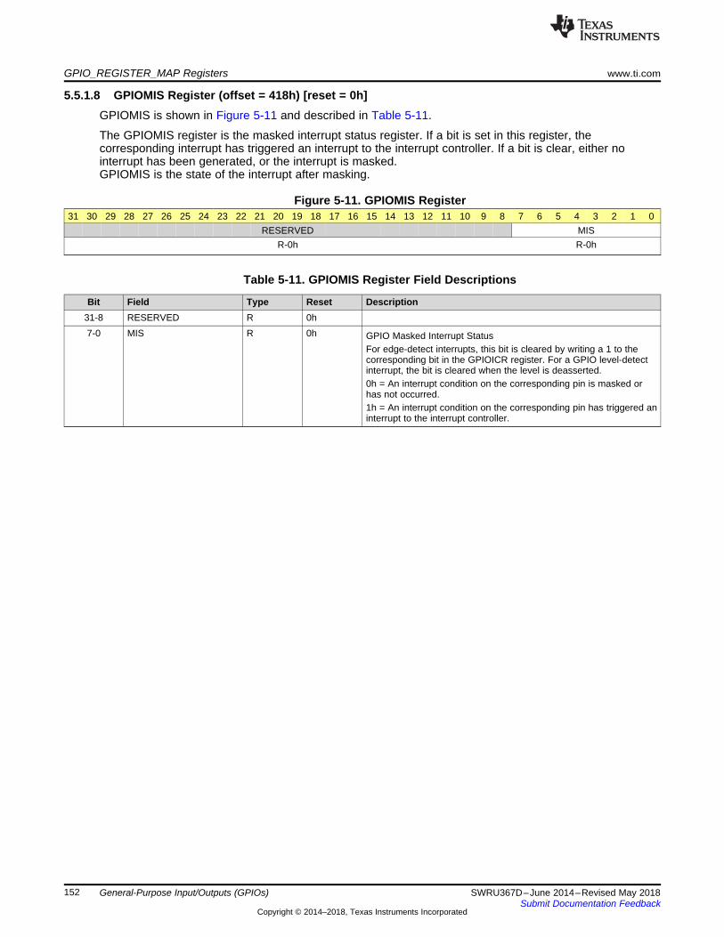
GPIO_REGISTER_MAP Registers www.ti.com
152 SWRU367D–June 2014–Revised May 2018Submit Documentation Feedback
Copyright © 2014–2018, Texas Instruments Incorporated
General-Purpose Input/Outputs (GPIOs)
5.5.1.8 GPIOMIS Register (offset = 418h) [reset = 0h]GPIOMIS is shown in Figure 5-11 and described in Table 5-11.
The GPIOMIS register is the masked interrupt status register. If a bit is set in this register, thecorresponding interrupt has triggered an interrupt to the interrupt controller. If a bit is clear, either nointerrupt has been generated, or the interrupt is masked.GPIOMIS is the state of the interrupt after masking.
Figure 5-11. GPIOMIS Register31 30 29 28 27 26 25 24 23 22 21 20 19 18 17 16 15 14 13 12 11 10 9 8 7 6 5 4 3 2 1 0
RESERVED MISR-0h R-0h
Table 5-11. GPIOMIS Register Field Descriptions
Bit Field Type Reset Description31-8 RESERVED R 0h7-0 MIS R 0h GPIO Masked Interrupt Status
For edge-detect interrupts, this bit is cleared by writing a 1 to thecorresponding bit in the GPIOICR register. For a GPIO level-detectinterrupt, the bit is cleared when the level is deasserted.0h = An interrupt condition on the corresponding pin is masked orhas not occurred.1h = An interrupt condition on the corresponding pin has triggered aninterrupt to the interrupt controller.
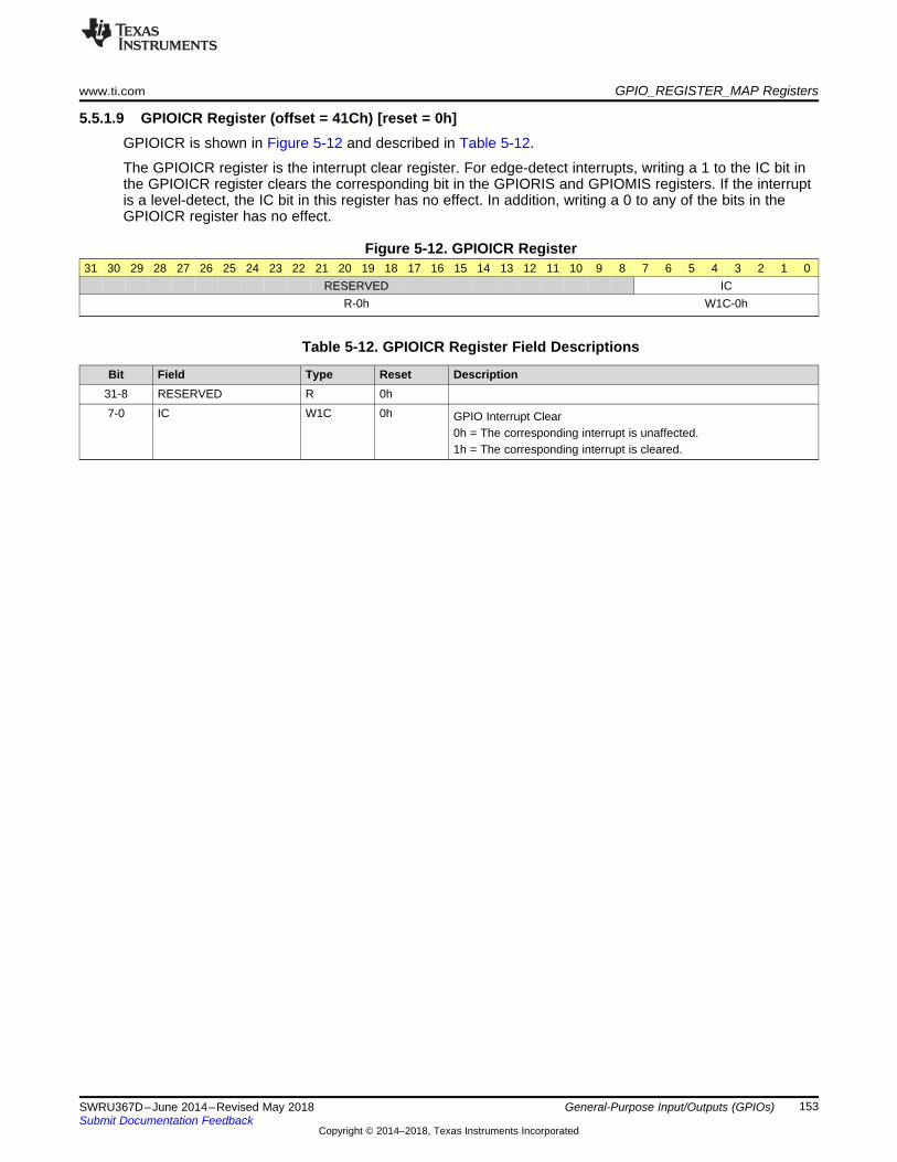
www.ti.com GPIO_REGISTER_MAP Registers
153SWRU367D–June 2014–Revised May 2018Submit Documentation Feedback
Copyright © 2014–2018, Texas Instruments Incorporated
General-Purpose Input/Outputs (GPIOs)
5.5.1.9 GPIOICR Register (offset = 41Ch) [reset = 0h]GPIOICR is shown in Figure 5-12 and described in Table 5-12.
The GPIOICR register is the interrupt clear register. For edge-detect interrupts, writing a 1 to the IC bit inthe GPIOICR register clears the corresponding bit in the GPIORIS and GPIOMIS registers. If the interruptis a level-detect, the IC bit in this register has no effect. In addition, writing a 0 to any of the bits in theGPIOICR register has no effect.
Figure 5-12. GPIOICR Register31 30 29 28 27 26 25 24 23 22 21 20 19 18 17 16 15 14 13 12 11 10 9 8 7 6 5 4 3 2 1 0
RESERVED ICR-0h W1C-0h
Table 5-12. GPIOICR Register Field Descriptions
Bit Field Type Reset Description31-8 RESERVED R 0h7-0 IC W1C 0h GPIO Interrupt Clear
0h = The corresponding interrupt is unaffected.1h = The corresponding interrupt is cleared.
GPIO_REGISTER_MAP Registers www.ti.com
154 SWRU367D–June 2014–Revised May 2018Submit Documentation Feedback
Copyright © 2014–2018, Texas Instruments Incorporated
General-Purpose Input/Outputs (GPIOs)
5.5.1.10 GPIO_TRIG_EN RegisterRegister Outside GPIO Module : GPIO Trigger Enable (GPIO_TRIG_EN): This register configures a GPIOpin as a source for the DMA trigger. Setting a bit in the GPIO_TRIG_EN register allows to trigger DMAupon any pin toggle correspond that GPIO module.
Physical Address: 0x400F 70C8.
Table 5-13. GPIO_TRIG_EN Register Field Descriptions
Bit Field Type Reset Description31-4 RESERVED R 0h3-0 TRIG R/W 0h GPIO DMA Trigger Enable.
Bit 0: when 1, enable GPIO 0 trigger. This bit enables trigger for allGPIO 0 pins (GPIO 0 to GPIO7).Bit 1: when 1, enable GPIO 1 trigger. This bit enables trigger for allGPIO 1 pins ( GPIO8 to GPIO15).Bit 2: when 1, enable GPIO 2 trigger. This bit enables trigger for allGPIO 2 pins (GPIO16 to GPIO23).Bit 3: when 1, enable GPIO 3 trigger. This bit enables trigger for allGPIO 3 pins (GPIO24 to GPIO31).
Table 5-14. GPIO Mapping
GPIO Module Instance GPIO Bit GPIO #GPIOA0 0 GPIO_00 (PM/Dig Mux)GPIOA0 1 GPIO_01GPIOA0 2 GPIO_02 (Dig/ADC Mux)GPIOA0 3 GPIO_03 (Dig/ADC Mux)GPIOA0 4 GPIO_04 (Dig/ADC Mux)GPIOA0 5 GPIO_05 (Dig/ADC Mux)GPIOA0 6 GPIO_06GPIOA0 7 GPIO_07GPIOA1 0 GPIO_08GPIOA1 1 GPIO_09GPIOA1 2 GPIO_10GPIOA1 3 GPIO_11GPIOA1 4 GPIO_12GPIOA1 5 GPIO_13GPIOA1 6 GPIO_14GPIOA1 7 GPIO_15GPIOA2 0 GPIO_16GPIOA2 1 GPIO_17GPIOA2 2 GPIO_18 (Reserved)GPIOA2 3 GPIO_19 (Reserved)GPIOA2 4 GPIO_20 (Reserved)GPIOA2 5 GPIO_21 (Reserved)GPIOA2 6 GPIO_22GPIOA2 7 GPIO_23GPIOA3 0 GPIO_24GPIOA3 1 GPIO_25
GPIOA3 2 GPIO_26 (Restricted Use; AntennaSelection 1 Only)
GPIOA3 3 GPIO_27 (Restricted Use; AntennaSelection 2 Only)
GPIOA3 4 GPIO_28
www.ti.com GPIO_REGISTER_MAP Registers
155SWRU367D–June 2014–Revised May 2018Submit Documentation Feedback
Copyright © 2014–2018, Texas Instruments Incorporated
General-Purpose Input/Outputs (GPIOs)
Table 5-14. GPIO Mapping (continued)GPIO Module Instance GPIO Bit GPIO #
GPIOA3 5 GPIO_29GPIOA3 6 GPIO_30 (PM/Dig Mux)GPIOA3 7 GPIO_31 (PM/Dig Mux)
156 SWRU367D–June 2014–Revised May 2018Submit Documentation Feedback
Copyright © 2014–2018, Texas Instruments Incorporated
Universal Asynchronous Receivers/Transmitters (UARTs)
Chapter 6SWRU367D–June 2014–Revised May 2018
Universal Asynchronous Receivers/Transmitters (UARTs)
Topic ........................................................................................................................... Page
6.1 Overview ......................................................................................................... 1576.2 Functional Description ...................................................................................... 1586.3 Register Description ......................................................................................... 163
www.ti.com Overview
157SWRU367D–June 2014–Revised May 2018Submit Documentation Feedback
Copyright © 2014–2018, Texas Instruments Incorporated
Universal Asynchronous Receivers/Transmitters (UARTs)
6.1 OverviewThe CC3200 includes two Universal Asynchronous Receivers/Transmitters (UART) with the followingfeatures:• Programmable baud-rate generator allowing speeds up to 3 Mbps.• Separate 16×8 transmit (TX) and receive (RX) FIFOs to reduce CPU interrupt service loading• Programmable FIFO length, including 1-byte deep operation providing conventional double-buffered
interface• FIFO trigger levels of 1/8, 1/4, 1/2, 3/4, and 7/8• Standard asynchronous communication bits for start, stop, and parity• Line-break generation and detection• Fully programmable serial interface characteristics
– 5, 6, 7, or 8 data bits– Even, odd, stick, or no-parity bit generation and detection– 1 or 2 stop bit generation
• RTS and CTS hardware flow support• Standard FIFO-level and end-of-transmission interrupts• Efficient transfers using micro-direct memory access controller (μDMA)
– Separate channels for transmit and receive– Receive single request asserted when data is in the FIFO; burst request asserted at programmed
FIFO level– Transmit single request asserted when there is space in the FIFO; burst request asserted at
programmed FIFO level• System clock generates the baud clock.
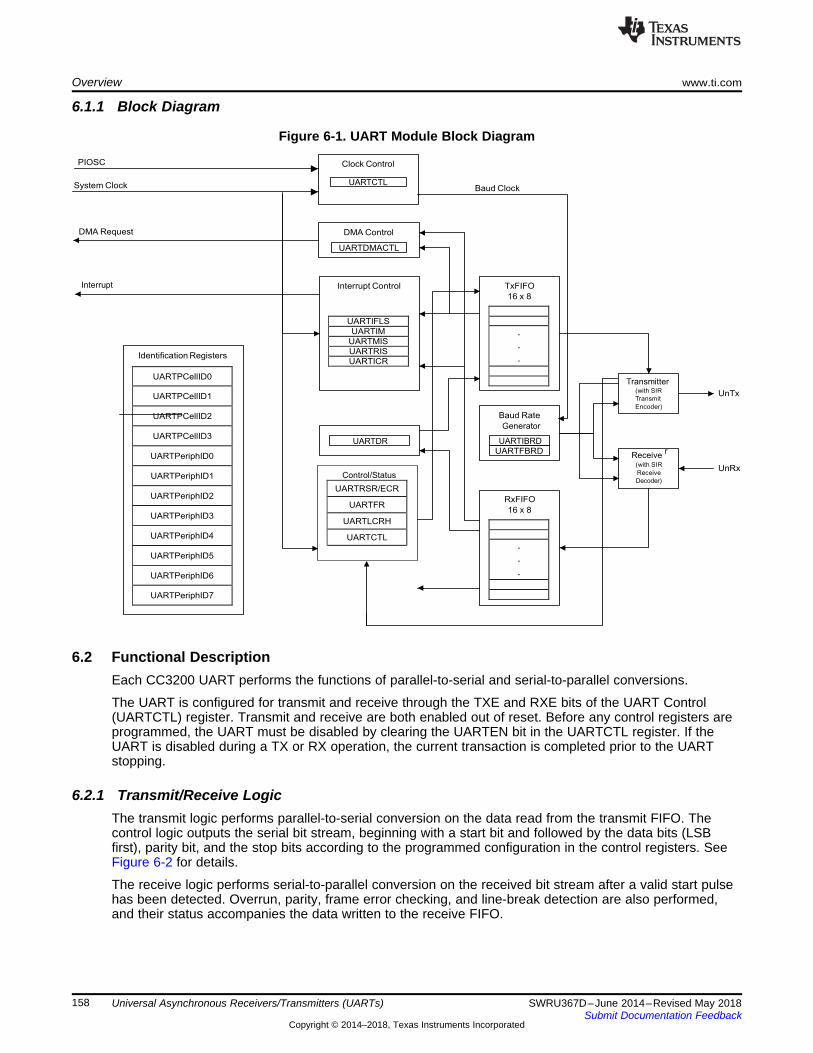
Overview www.ti.com
158 SWRU367D–June 2014–Revised May 2018Submit Documentation Feedback
Copyright © 2014–2018, Texas Instruments Incorporated
Universal Asynchronous Receivers/Transmitters (UARTs)
6.1.1 Block Diagram
Figure 6-1. UART Module Block Diagram
6.2 Functional DescriptionEach CC3200 UART performs the functions of parallel-to-serial and serial-to-parallel conversions.
The UART is configured for transmit and receive through the TXE and RXE bits of the UART Control(UARTCTL) register. Transmit and receive are both enabled out of reset. Before any control registers areprogrammed, the UART must be disabled by clearing the UARTEN bit in the UARTCTL register. If theUART is disabled during a TX or RX operation, the current transaction is completed prior to the UARTstopping.
6.2.1 Transmit/Receive LogicThe transmit logic performs parallel-to-serial conversion on the data read from the transmit FIFO. Thecontrol logic outputs the serial bit stream, beginning with a start bit and followed by the data bits (LSBfirst), parity bit, and the stop bits according to the programmed configuration in the control registers. SeeFigure 6-2 for details.
The receive logic performs serial-to-parallel conversion on the received bit stream after a valid start pulsehas been detected. Overrun, parity, frame error checking, and line-break detection are also performed,and their status accompanies the data written to the receive FIFO.

www.ti.com Functional Description
159SWRU367D–June 2014–Revised May 2018Submit Documentation Feedback
Copyright © 2014–2018, Texas Instruments Incorporated
Universal Asynchronous Receivers/Transmitters (UARTs)
Figure 6-2. UART Character Frame
6.2.2 Baud-Rate GenerationThe baud-rate divisor is a 22-bit number consisting of a 16-bit integer and a 6-bit fractional part. Thenumber formed by these two values is used by the baud-rate generator to determine the bit period. Havinga fractional baud-rate divisor allows the UART to generate all the standard baud rates.
The 16-bit integer is loaded through the UART Integer Baud-Rate Divisor (UARTIBRD) register and the 6-bit fractional part is loaded with the UART Fractional Baud-Rate Divisor (UARTFBRD) register . The baud-rate divisor (BRD) has the following relationship to the system clock (where BRDI is the integer part of theBRD and BRDF is the fractional part, separated by a decimal place.)
BRD = BRDI + BRDF = UARTSysClk / (ClkDiv * Baud Rate)
where UARTSysClk is the system clock connected to the UART, and ClkDiv is either 16 (if HSE inUARTCTL is clear) or 8 (if HSE is set). By default, this is the main system clock described inSection 15.4.5.
The 6-bit fractional number (loaded into the DIVFRAC bit field in the UARTFBRD register) can becalculated by taking the fractional part of the baud-rate divisor, multiplying it by 64, and adding 0.5 toaccount for rounding errors:
UARTFBRD[DIVFRAC] = integer(BRDF * 64 + 0.5)
The UART generates an internal baud-rate reference clock at 8× or 16× the baud-rate (referred to asBaud8 and Baud16, depending on the setting of the HSE bit (bit 5) in UARTCTL). This reference clock isdivided by 8 or 16 to generate the transmit clock, and used for error detection during receive operations.
Along with the UART Line Control, High Byte (UARTLCRH) register, the UARTIBRD and UARTFBRDregisters form an internal 30-bit register. This internal register is only updated when a write operation toUARTLCRH is performed, so any changes to the baud-rate divisor must be followed by a write to theUARTLCRH register for the changes to take effect. To update the baud-rate registers, there are fourpossible sequences:• UARTI BRD write, UARTF BRD write, and UARTLCRH write• UARTF BRD write, UARTI BRD write, and UARTLCRH write• UARTI BRD write and UARTLCRH write• UARTF BRD write and UARTLCRH write
6.2.3 Data TransmissionData received or transmitted is stored in two 16-byte FIFOs, though the receive FIFO has an extra fourbits per character for status information. For transmission, data is written into the transmit FIFO. If theUART is enabled, it causes a data frame to start transmitting with the parameters indicated in theUARTLCRH register. Data continues to be transmitted until there is no data left in the transmit FIFO. TheBUSY bit in the UART Flag (UARTFR) register is asserted when data is written to the transmit FIFO (if theFIFO is non-empty) and remains asserted while data is being transmitted. The BUSY bit is negated onlywhen the transmit FIFO is empty, and the last character has been transmitted from the shift register,including the stop bits. The UART can indicate that it is busy even though the UART may no longer beenabled.
When the receiver is idle (the UnRx signal is continuously 1), and the data input goes low (a start bit hasbeen received), the receive counter begins running and data is sampled on the eighth cycle of Baud16 orfourth cycle of Baud8 depending on the setting of the HSE bit (bit 5) in UARTCTL.
Functional Description www.ti.com
160 SWRU367D–June 2014–Revised May 2018Submit Documentation Feedback
Copyright © 2014–2018, Texas Instruments Incorporated
Universal Asynchronous Receivers/Transmitters (UARTs)
The start bit is valid and recognized if the UnRx signal is still low on the eighth cycle of Baud16 (HSEclear) or the fourth cycle of Baud8 (HSE set), otherwise it is ignored. After a valid start bit is detected,successive data bits are sampled on every 16th cycle of Baud16 or 8th cycle of Baud8 (that is, one bitperiod later) according to the programmed length of the data characters and value of the HSE bit inUARTCTL. The parity bit is then checked if parity mode is enabled. Data length and parity are defined inthe UARTLCRH register.
Lastly, a valid stop bit is confirmed if the UnRx signal is high, otherwise a framing error has occurred.When a full word is received, the data is stored in the receive FIFO along with any error bits associatedwith that word.
6.2.3.1 Flow ControlFlow control can be accomplished by either hardware or software. The following sections describe thedifferent methods.
6.2.3.1.1 Hardware Flow Control (RTS/CTS)Hardware flow control between two devices is accomplished by connecting the U1RTS output to the clear-to-send input on the receiving device, and connecting the request-to-send output on the receiving deviceto the U1RTS input.
The U1RTS input controls the transmitter. The transmitter may only transmit data when the U1RTS inputis asserted. The U1RTS output signal indicates the state of the receive FIFO. U1CTS remains asserteduntil the preprogrammed watermark level is reached, indicating that the receive FIFO has no space tostore additional characters.
The UARTCTL register bits 15 (CTSEN) and 14 (RTSEN) specify the flow control mode as shown inTable 6-1.
Table 6-1. Flow Control Mode
CTSEN RTSEN Description
1 1 RTS and CTS flow controlenabled
1 0 Only CTS flow control enabled
0 1 Only RTS Flow Controlenabled
0 0 Both RTS and CTS flow controldisabled
When RTSEN is 1, software cannot modify the U1RTS output value through the UARTCTL registerrequest-to-send (RTS) bit, and the status of the RTS bit should be ignored.
6.2.3.1.2 Software Flow Control (Modem Status Interrupts)Software flow control between two devices is accomplished by using interrupts to indicate the status of theUART. Interrupts may be generated for the U1CTS and U1RI signals using bit 1 of the UARTIM register,respectively. The raw and masked interrupt status may be checked using the UARTRIS and UARTMISregisters. These interrupts may be cleared using the UARTICR register.
6.2.3.2 FIFO OperationThe UART has two 16×8 FIFOs; one for transmit and one for receive. Both FIFOs are accessed throughthe UART Data (UARTDR) register. Read operations of the UARTDR register return a 12-bit valueconsisting of 8 data bits and 4 error flags, while write operations place 8-bit data in the transmit FIFO.
Out of reset, both FIFOs are disabled and act as 1-byte-deep holding registers. The FIFOs are enabled bysetting the FEN bit in UARTLCRH.
www.ti.com Functional Description
161SWRU367D–June 2014–Revised May 2018Submit Documentation Feedback
Copyright © 2014–2018, Texas Instruments Incorporated
Universal Asynchronous Receivers/Transmitters (UARTs)
FIFO status can be monitored via the UART Flag (UARTFR) register and the UART Receive Status(UARTRSR) register. Hardware monitors empty, full, and overrun conditions. The UARTFR registercontains empty and full flags (TXFE, TXFF, RXFE, and RXFF bits), and the UARTRSR register showsoverrun status through the OE bit. If the FIFOs are disabled, the empty and full flags are set according tothe status of the 1-byte-deep holding registers.
The trigger points at which the FIFOs generate interrupts are controlled through the UART Interrupt FIFOLevel Select (UARTIFLS) register. Both FIFOs can be individually configured to trigger interrupts atdifferent levels. Available configurations include ⅛,¼, ½, ¾, and ⅞. For example, if the ¼ option isselected for the receive FIFO, the UART generates a receive interrupt after 4 data bytes are received. Outof reset, both FIFOs are configured to trigger an interrupt at the ½ mark.
6.2.3.3 InterruptsThe UART can generate interrupts when the following conditions are observed:• Overrun error• Break error• Parity error• Framing error• Receive timeout• Transmit (when the condition defined in the TXIFLSEL bit in the UARTIFLS register is met, or if the
EOT bit in UARTCTL is set, when the last bit of all transmitted data leaves the serializer)• Receive (when the condition defined in the RXIFLSEL bit in the UARTIFLS register is met)
All of the interrupt events are ORed together before being sent to the interrupt controller, so the UART canonly generate a single interrupt request to the controller at any given time. Software can service multipleinterrupt events in a single interrupt service routine by reading the UART Masked Interrupt Status(UARTMIS) register.
The interrupt events that can trigger a controller-level interrupt are defined in the UART Interrupt Mask(UARTIM) register by setting the corresponding IM bits. If interrupts are not used, the raw interrupt statusis always visible through the UART Raw Interrupt Status (UARTRIS) register.
Interrupts are always cleared (for both the UARTMIS and UARTRIS registers) by writing a 1 to thecorresponding bit in the UART Interrupt Clear (UARTICR) register.
The receive timeout interrupt is asserted when the receive FIFO is not empty, and no further data isreceived over a 32-bit period when the HSE bit is clear, or over a 64-bit period when the HSE bit is set.The receive timeout interrupt is cleared either when the FIFO becomes empty through reading all the data(or by reading the holding register), or when a 1 is written to the corresponding bit in the UARTICRregister.
The receive interrupt changes state when one of the following events occurs:• If the FIFOs are enabled and the receive FIFO reaches the programmed trigger level, the RXRIS bit is
set. The receive interrupt is cleared by reading data from the receive FIFO until it becomes less thanthe trigger level, or by clearing the interrupt by writing a 1 to the RXIC bit.
• If the FIFOs are disabled (have a depth of one location) and data is received thereby filling thelocation, the RXRIS bit is set. The receive interrupt is cleared by performing a single read of thereceive FIFO, or by clearing the interrupt by writing a 1 to the RXIC bit.
The transmit interrupt changes state when one of the following events occurs:• If the FIFOs are enabled and the transmit FIFO progresses through the programmed trigger level, the
TXRIS bit is set. The transmit interrupt is based on a transition through level, therefore the FIFO mustbe written past the programmed trigger level or no further transmit interrupts will be generated. Thetransmit interrupt is cleared by writing data to the transmit FIFO until it becomes greater than thetrigger level, or by clearing the interrupt by writing a 1 to the TXIC bit.
• If the FIFOs are disabled (have a depth of one location) and there is no data present in the transmitterssingle location, the TXRIS bit is set. It is cleared by performing a single write to the transmit FIFO, orby clearing the interrupt by writing a 1 to the TXIC bit.
Functional Description www.ti.com
162 SWRU367D–June 2014–Revised May 2018Submit Documentation Feedback
Copyright © 2014–2018, Texas Instruments Incorporated
Universal Asynchronous Receivers/Transmitters (UARTs)
6.2.3.4 LoopbackOperationThe UART can be placed into an internal loopback mode for diagnostic or debug work by setting the LBEbit in the UARTCTL register. In loopback mode, data transmitted on the UnTx output is received on theUnRx input. Note that the LBE bit should be set before the UART is enabled.
6.2.3.5 DMA OperationThe UART provides an interface to the μDMA controller with separate channels for transmit and receive.The DMA operation of the UART is enabled through the UART DMA Control (UARTDMACTL) register.When DMA operation is enabled, the UART asserts a DMA request on the receive or transmit channelwhen the associated FIFO can transfer data. For the receive channel, a single transfer request is assertedwhenever any data is in the receive FIFO. A burst transfer request is asserted whenever the amount ofdata in the receive FIFO is at or above the FIFO trigger level configured in the UARTIFLS register. For thetransmit channel, a single transfer request is asserted whenever there is at least one empty location in thetransmit FIFO. The burst request is asserted whenever the transmit FIFO contains fewer characters thanthe FIFO trigger level. The single and burst DMA transfer requests are handled automatically by the μDMAcontroller, depending on how the DMA channel is configured.
To enable DMA operation for the receive channel, set the RXDMAE bit of the DMA Control(UARTDMACTL) register. To enable DMA operation for the transmit channel, set the TXDMAE bit of theUARTDMACTL register. The UART can also be configured to stop using DMA for the receive channel if areceive error occurs. If the DMAERR bit of the UARTDMACR register is set and a receive error occurs,the DMA receive requests are automatically disabled. This error condition can be cleared by clearing theappropriate UART error interrupt.
If DMA is enabled, then the μDMA controller triggers an interrupt when a transfer is complete. Theinterrupt occurs on the UART interrupt vector. Therefore, if interrupts are used for UART operation andDMA is enabled, the UART interrupt handler must be designed to handle the μDMA completion interrupt.
6.2.4 Initialization and ConfigurationTo enable and initialize the UART, the following steps are necessary:1. Enable the UART module using the UART0CLKEN/UART1CLKEN register.2. Set the GPIO_PAD_CONFIG CONFMODE bits for the appropriate pins.
This section discusses the steps required to use a UART module. For this example, the UART clock isassumed to be 80 MHz, and the desired UART configuration is:• 115200 baud rate• Data length of 8 bits• One stop bit• No parity• FIFOs disabled• No interrupts
The first thing to consider when programming the UART is the baud-rate divisor (BRD), because theUARTI BRD and UARTF BRD registers must be written before the UARTLCRH register. Using theequation described in Section 6.2.2, the BRD can be calculated:BRD = 80,000,000 / (16 * 115,200) =
43.410590
which means that the DIVINT field of the UARTIBRD register should be set to 43 decimal or 0x2B. Thevalue to be loaded into the UARTFBRD register is calculated by the equation:UARTFBRD[DIVFRAC] = integer(0.410590 * 64 +
0.5) = 26
With the BRD values in hand, the UART configuration is written to the module in the following order:1. Disable the UART by clearing the UARTEN bit in the UARTCTL register.2. Write the integer portion of the BRD to the UARTIBRD register.
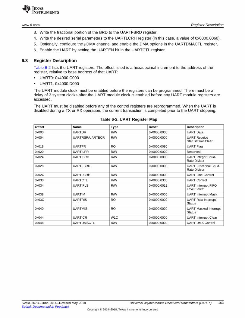
www.ti.com Register Description
163SWRU367D–June 2014–Revised May 2018Submit Documentation Feedback
Copyright © 2014–2018, Texas Instruments Incorporated
Universal Asynchronous Receivers/Transmitters (UARTs)
3. Write the fractional portion of the BRD to the UARTFBRD register.4. Write the desired serial parameters to the UARTLCRH register (in this case, a value of 0x0000.0060).5. Optionally, configure the μDMA channel and enable the DMA options in the UARTDMACTL register.6. Enable the UART by setting the UARTEN bit in the UARTCTL register.
6.3 Register DescriptionTable 6-2 lists the UART registers. The offset listed is a hexadecimal increment to the address of theregister, relative to base address of that UART:• UART0: 0x4000.C000• UART1: 0x4000.D000
The UART module clock must be enabled before the registers can be programmed. There must be adelay of 3 system clocks after the UART module clock is enabled before any UART module registers areaccessed.
The UART must be disabled before any of the control registers are reprogrammed. When the UART isdisabled during a TX or RX operation, the current transaction is completed prior to the UART stopping.
Table 6-2. UART Register Map
Offset Name Type Reset Description0x000 UARTDR R/W 0x0000.0000 UART Data0x004 UARTRSR/UARTECR R/W 0x0000.0000 UART Receive
Status/Error Clear0x018 UARTFR RO 0x0000.0090 UART Flag0x020 UARTILPR R/W 0x0000.0000 Reserved0x024 UARTIBRD R/W 0x0000.0000 UART Integer Baud-
Rate Divisor0x028 UARTFBRD R/W 0x0000.0000 UART Fractional Baud-
Rate Divisor0x02C UARTLCRH R/W 0x0000.0000 UART Line Control0x030 UARTCTL R/W 0x0000.0300 UART Control0x034 UARTIFLS R/W 0x0000.0012 UART Interrupt FIFO
Level Select0x038 UARTIM R/W 0x0000.0000 UART Interrupt Mask0x03C UARTRIS RO 0x0000.0000 UART Raw Interrupt
Status0x040 UARTMIS RO 0x0000.0000 UART Masked Interrupt
Status0x044 UARTICR W1C 0x0000.0000 UART Interrupt Clear0x048 UARTDMACTL R/W 0x0000.0000 UART DMA Control
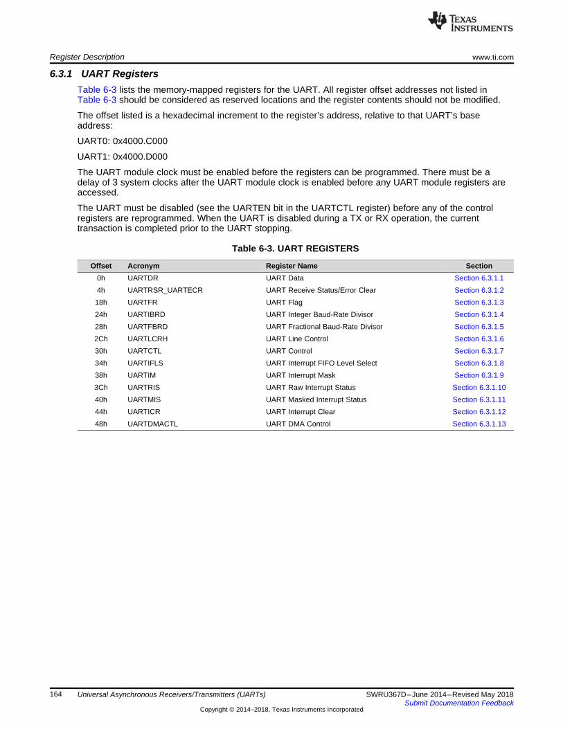
Register Description www.ti.com
164 SWRU367D–June 2014–Revised May 2018Submit Documentation Feedback
Copyright © 2014–2018, Texas Instruments Incorporated
Universal Asynchronous Receivers/Transmitters (UARTs)
6.3.1 UART RegistersTable 6-3 lists the memory-mapped registers for the UART. All register offset addresses not listed inTable 6-3 should be considered as reserved locations and the register contents should not be modified.
The offset listed is a hexadecimal increment to the register’s address, relative to that UART’s baseaddress:
UART0: 0x4000.C000
UART1: 0x4000.D000
The UART module clock must be enabled before the registers can be programmed. There must be adelay of 3 system clocks after the UART module clock is enabled before any UART module registers areaccessed.
The UART must be disabled (see the UARTEN bit in the UARTCTL register) before any of the controlregisters are reprogrammed. When the UART is disabled during a TX or RX operation, the currenttransaction is completed prior to the UART stopping.
Table 6-3. UART REGISTERS
Offset Acronym Register Name Section0h UARTDR UART Data Section 6.3.1.14h UARTRSR_UARTECR UART Receive Status/Error Clear Section 6.3.1.218h UARTFR UART Flag Section 6.3.1.324h UARTIBRD UART Integer Baud-Rate Divisor Section 6.3.1.428h UARTFBRD UART Fractional Baud-Rate Divisor Section 6.3.1.52Ch UARTLCRH UART Line Control Section 6.3.1.630h UARTCTL UART Control Section 6.3.1.734h UARTIFLS UART Interrupt FIFO Level Select Section 6.3.1.838h UARTIM UART Interrupt Mask Section 6.3.1.93Ch UARTRIS UART Raw Interrupt Status Section 6.3.1.1040h UARTMIS UART Masked Interrupt Status Section 6.3.1.1144h UARTICR UART Interrupt Clear Section 6.3.1.1248h UARTDMACTL UART DMA Control Section 6.3.1.13
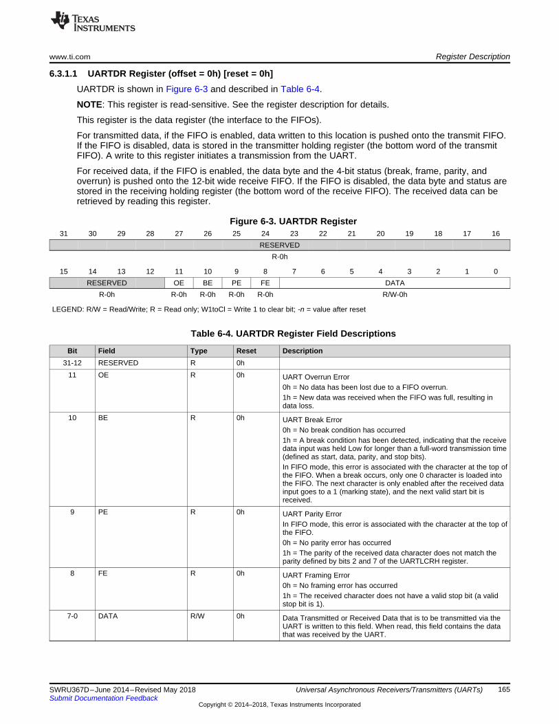
www.ti.com Register Description
165SWRU367D–June 2014–Revised May 2018Submit Documentation Feedback
Copyright © 2014–2018, Texas Instruments Incorporated
Universal Asynchronous Receivers/Transmitters (UARTs)
6.3.1.1 UARTDR Register (offset = 0h) [reset = 0h]UARTDR is shown in Figure 6-3 and described in Table 6-4.
NOTE: This register is read-sensitive. See the register description for details.
This register is the data register (the interface to the FIFOs).
For transmitted data, if the FIFO is enabled, data written to this location is pushed onto the transmit FIFO.If the FIFO is disabled, data is stored in the transmitter holding register (the bottom word of the transmitFIFO). A write to this register initiates a transmission from the UART.
For received data, if the FIFO is enabled, the data byte and the 4-bit status (break, frame, parity, andoverrun) is pushed onto the 12-bit wide receive FIFO. If the FIFO is disabled, the data byte and status arestored in the receiving holding register (the bottom word of the receive FIFO). The received data can beretrieved by reading this register.
Figure 6-3. UARTDR Register31 30 29 28 27 26 25 24 23 22 21 20 19 18 17 16
RESERVEDR-0h
15 14 13 12 11 10 9 8 7 6 5 4 3 2 1 0RESERVED OE BE PE FE DATA
R-0h R-0h R-0h R-0h R-0h R/W-0h
LEGEND: R/W = Read/Write; R = Read only; W1toCl = Write 1 to clear bit; -n = value after reset
Table 6-4. UARTDR Register Field Descriptions
Bit Field Type Reset Description31-12 RESERVED R 0h
11 OE R 0h UART Overrun Error0h = No data has been lost due to a FIFO overrun.1h = New data was received when the FIFO was full, resulting indata loss.
10 BE R 0h UART Break Error0h = No break condition has occurred1h = A break condition has been detected, indicating that the receivedata input was held Low for longer than a full-word transmission time(defined as start, data, parity, and stop bits).In FIFO mode, this error is associated with the character at the top ofthe FIFO. When a break occurs, only one 0 character is loaded intothe FIFO. The next character is only enabled after the received datainput goes to a 1 (marking state), and the next valid start bit isreceived.
9 PE R 0h UART Parity ErrorIn FIFO mode, this error is associated with the character at the top ofthe FIFO.0h = No parity error has occurred1h = The parity of the received data character does not match theparity defined by bits 2 and 7 of the UARTLCRH register.
8 FE R 0h UART Framing Error0h = No framing error has occurred1h = The received character does not have a valid stop bit (a validstop bit is 1).
7-0 DATA R/W 0h Data Transmitted or Received Data that is to be transmitted via theUART is written to this field. When read, this field contains the datathat was received by the UART.
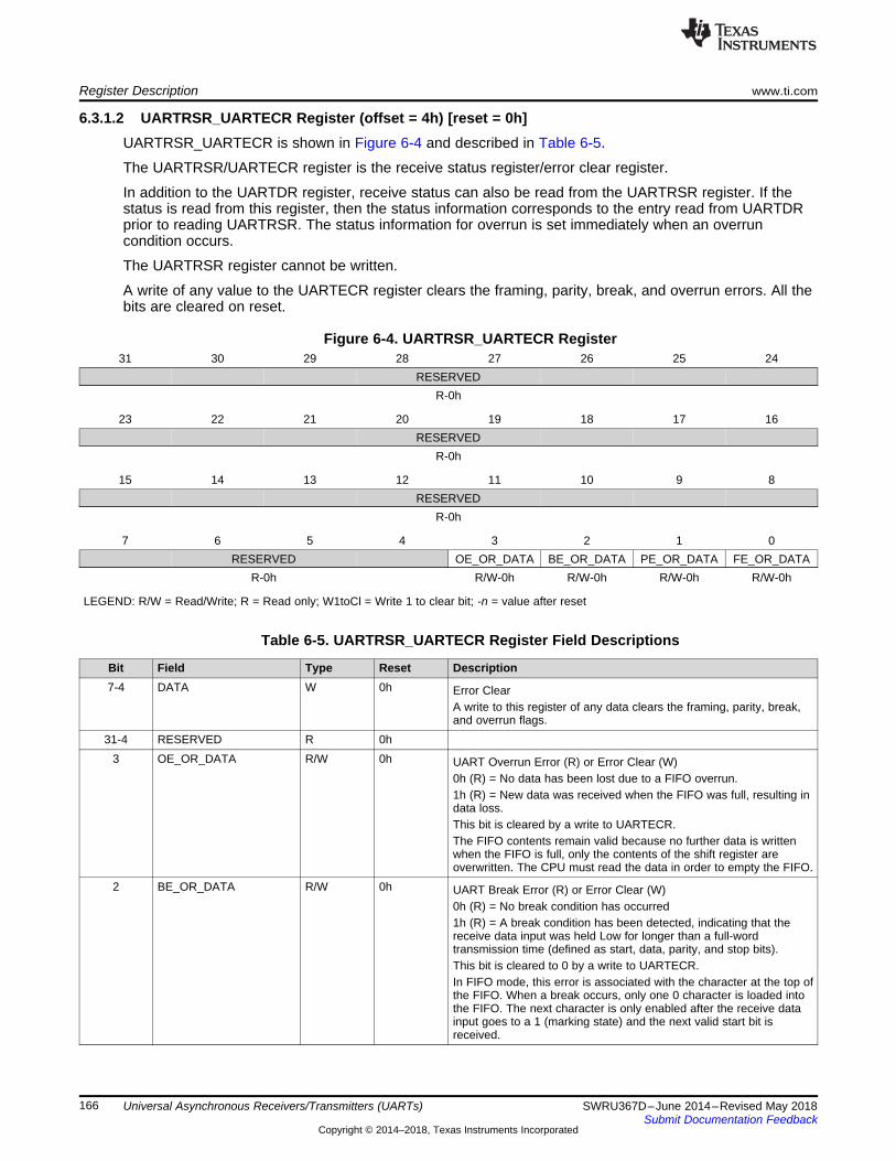
Register Description www.ti.com
166 SWRU367D–June 2014–Revised May 2018Submit Documentation Feedback
Copyright © 2014–2018, Texas Instruments Incorporated
Universal Asynchronous Receivers/Transmitters (UARTs)
6.3.1.2 UARTRSR_UARTECR Register (offset = 4h) [reset = 0h]UARTRSR_UARTECR is shown in Figure 6-4 and described in Table 6-5.
The UARTRSR/UARTECR register is the receive status register/error clear register.
In addition to the UARTDR register, receive status can also be read from the UARTRSR register. If thestatus is read from this register, then the status information corresponds to the entry read from UARTDRprior to reading UARTRSR. The status information for overrun is set immediately when an overruncondition occurs.
The UARTRSR register cannot be written.
A write of any value to the UARTECR register clears the framing, parity, break, and overrun errors. All thebits are cleared on reset.
Figure 6-4. UARTRSR_UARTECR Register31 30 29 28 27 26 25 24
RESERVEDR-0h
23 22 21 20 19 18 17 16RESERVED
R-0h
15 14 13 12 11 10 9 8RESERVED
R-0h
7 6 5 4 3 2 1 0RESERVED OE_OR_DATA BE_OR_DATA PE_OR_DATA FE_OR_DATA
R-0h R/W-0h R/W-0h R/W-0h R/W-0h
LEGEND: R/W = Read/Write; R = Read only; W1toCl = Write 1 to clear bit; -n = value after reset
Table 6-5. UARTRSR_UARTECR Register Field Descriptions
Bit Field Type Reset Description7-4 DATA W 0h Error Clear
A write to this register of any data clears the framing, parity, break,and overrun flags.
31-4 RESERVED R 0h3 OE_OR_DATA R/W 0h UART Overrun Error (R) or Error Clear (W)
0h (R) = No data has been lost due to a FIFO overrun.1h (R) = New data was received when the FIFO was full, resulting indata loss.This bit is cleared by a write to UARTECR.The FIFO contents remain valid because no further data is writtenwhen the FIFO is full, only the contents of the shift register areoverwritten. The CPU must read the data in order to empty the FIFO.
2 BE_OR_DATA R/W 0h UART Break Error (R) or Error Clear (W)0h (R) = No break condition has occurred1h (R) = A break condition has been detected, indicating that thereceive data input was held Low for longer than a full-wordtransmission time (defined as start, data, parity, and stop bits).This bit is cleared to 0 by a write to UARTECR.In FIFO mode, this error is associated with the character at the top ofthe FIFO. When a break occurs, only one 0 character is loaded intothe FIFO. The next character is only enabled after the receive datainput goes to a 1 (marking state) and the next valid start bit isreceived.
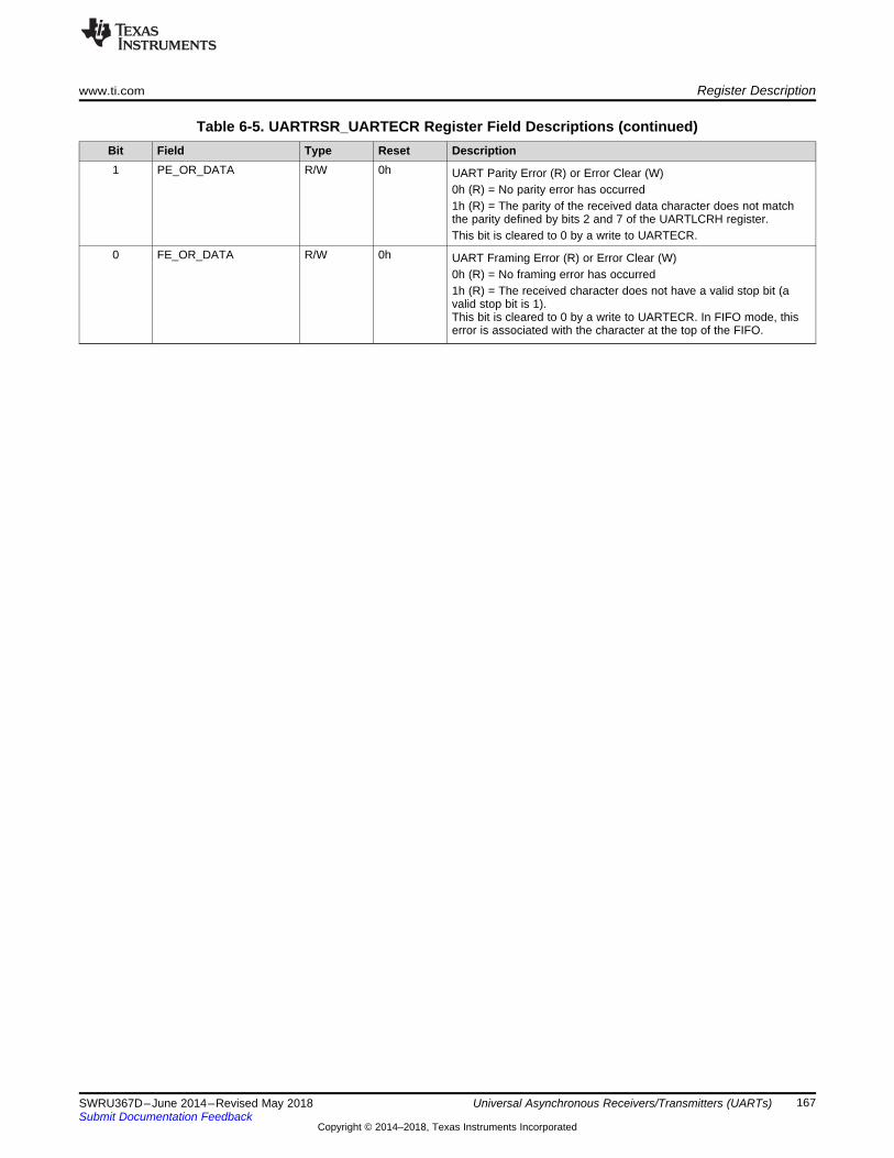
www.ti.com Register Description
167SWRU367D–June 2014–Revised May 2018Submit Documentation Feedback
Copyright © 2014–2018, Texas Instruments Incorporated
Universal Asynchronous Receivers/Transmitters (UARTs)
Table 6-5. UARTRSR_UARTECR Register Field Descriptions (continued)Bit Field Type Reset Description1 PE_OR_DATA R/W 0h UART Parity Error (R) or Error Clear (W)
0h (R) = No parity error has occurred1h (R) = The parity of the received data character does not matchthe parity defined by bits 2 and 7 of the UARTLCRH register.This bit is cleared to 0 by a write to UARTECR.
0 FE_OR_DATA R/W 0h UART Framing Error (R) or Error Clear (W)0h (R) = No framing error has occurred1h (R) = The received character does not have a valid stop bit (avalid stop bit is 1).This bit is cleared to 0 by a write to UARTECR. In FIFO mode, thiserror is associated with the character at the top of the FIFO.

Register Description www.ti.com
168 SWRU367D–June 2014–Revised May 2018Submit Documentation Feedback
Copyright © 2014–2018, Texas Instruments Incorporated
Universal Asynchronous Receivers/Transmitters (UARTs)
6.3.1.3 UARTFR Register (offset = 18h) [reset = 90h]UARTFR is shown in Figure 6-5 and described in Table 6-6.The UARTFR register is the flag register. Afterreset, the TXFF, RXFF, and BUSY bits are 0, and TXFE and RXFE bits are 1. The RI and CTS bitsindicate the modem flow control and status. Note that the modem bits are only implemented on UART1and are reserved on UART0.
Figure 6-5. UARTFR Register31 30 29 28 27 26 25 24
RESERVEDR-0h
23 22 21 20 19 18 17 16RESERVED
R-0h
15 14 13 12 11 10 9 8RESERVED RI
R-0h R-0h
7 6 5 4 3 2 1 0TXFE RXFF TXFF EXFE BUSY DCD DSR CTSR-1h R-0h R-0h R-1h R-0h R-0h R-0h R-0h
LEGEND: R/W = Read/Write; R = Read only; W1toCl = Write 1 to clear bit; -n = value after reset
Table 6-6. UARTFR Register Field Descriptions
Bit Field Type Reset Description31-9 RESERVED R 0h
8 RI R 0h Reserved7 TXFE R 1h UART Transmit FIFO Empty
The meaning of this bit depends on the state of the FEN bit in theUARTLCRH register.0h = The transmitter has data to transmit.1h = If the FIFO is disabled (FEN is 0), the transmit holding registeris empty.If the FIFO is enabled (FEN is 1), the transmit FIFO is empty.
6 RXFF R 0h UART Receive FIFO FullThe meaning of this bit depends on the state of the FEN bit in theUARTLCRH register.0h = The receiver can receive data.1h = If the FIFO is disabled (FEN is 0), the receive holding register isfull.If the FIFO is enabled (FEN is 1), the receive FIFO is full.
5 TXFF R 0h UART Transmit FIFO FullThe meaning of this bit depends on the state of the FEN bit in theUARTLCRH register.0h = The transmitter is not full.1h = If the FIFO is disabled (FEN is 0), the transmit holding registeris full. If the FIFO is enabled (FEN is 1), the transmit FIFO is full.
4 EXFE R 1h UART Receive FIFO EmptyThe meaning of this bit depends on the state of the FEN bit in theUARTLCRH register.0h = The receiver is not empty.1h = If the FIFO is disabled (FEN is 0), the receive holding register isempty.If the FIFO is enabled (FEN is 1), the receive FIFO is empty.
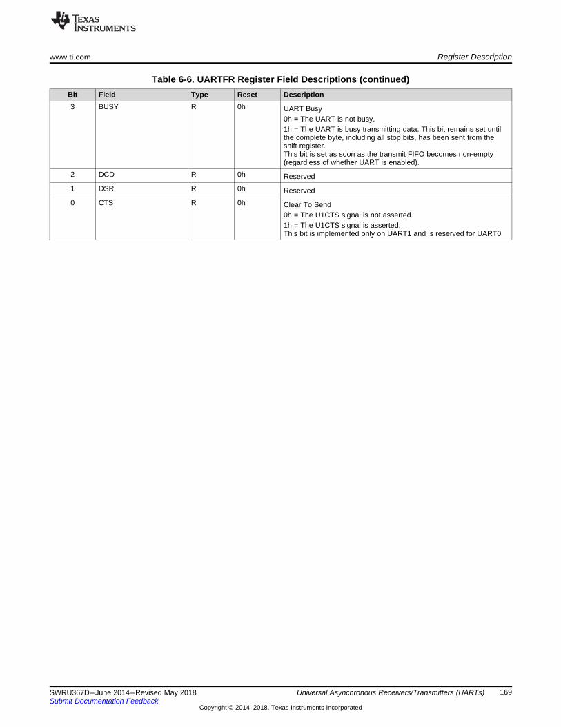
www.ti.com Register Description
169SWRU367D–June 2014–Revised May 2018Submit Documentation Feedback
Copyright © 2014–2018, Texas Instruments Incorporated
Universal Asynchronous Receivers/Transmitters (UARTs)
Table 6-6. UARTFR Register Field Descriptions (continued)Bit Field Type Reset Description3 BUSY R 0h UART Busy
0h = The UART is not busy.1h = The UART is busy transmitting data. This bit remains set untilthe complete byte, including all stop bits, has been sent from theshift register.This bit is set as soon as the transmit FIFO becomes non-empty(regardless of whether UART is enabled).
2 DCD R 0h Reserved1 DSR R 0h Reserved0 CTS R 0h Clear To Send
0h = The U1CTS signal is not asserted.1h = The U1CTS signal is asserted.This bit is implemented only on UART1 and is reserved for UART0
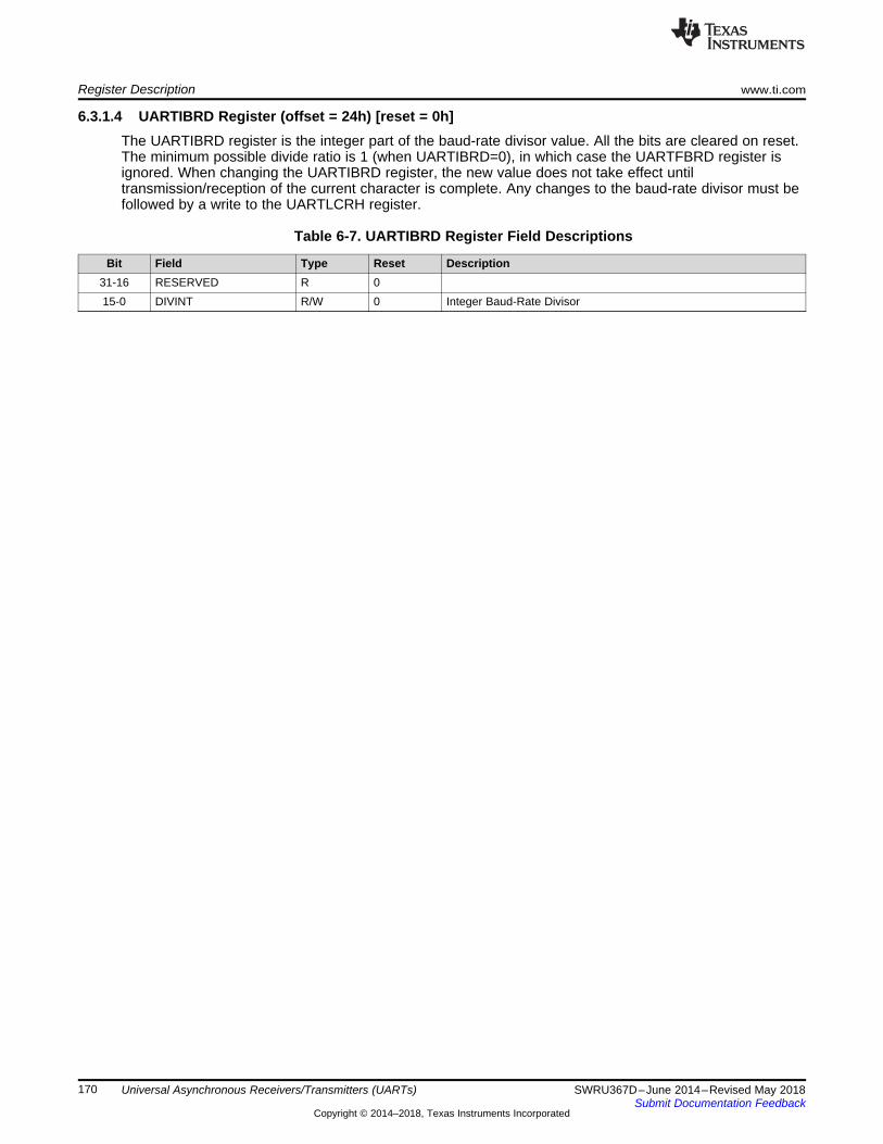
Register Description www.ti.com
170 SWRU367D–June 2014–Revised May 2018Submit Documentation Feedback
Copyright © 2014–2018, Texas Instruments Incorporated
Universal Asynchronous Receivers/Transmitters (UARTs)
6.3.1.4 UARTIBRD Register (offset = 24h) [reset = 0h]The UARTIBRD register is the integer part of the baud-rate divisor value. All the bits are cleared on reset.The minimum possible divide ratio is 1 (when UARTIBRD=0), in which case the UARTFBRD register isignored. When changing the UARTIBRD register, the new value does not take effect untiltransmission/reception of the current character is complete. Any changes to the baud-rate divisor must befollowed by a write to the UARTLCRH register.
Table 6-7. UARTIBRD Register Field Descriptions
Bit Field Type Reset Description31-16 RESERVED R 015-0 DIVINT R/W 0 Integer Baud-Rate Divisor
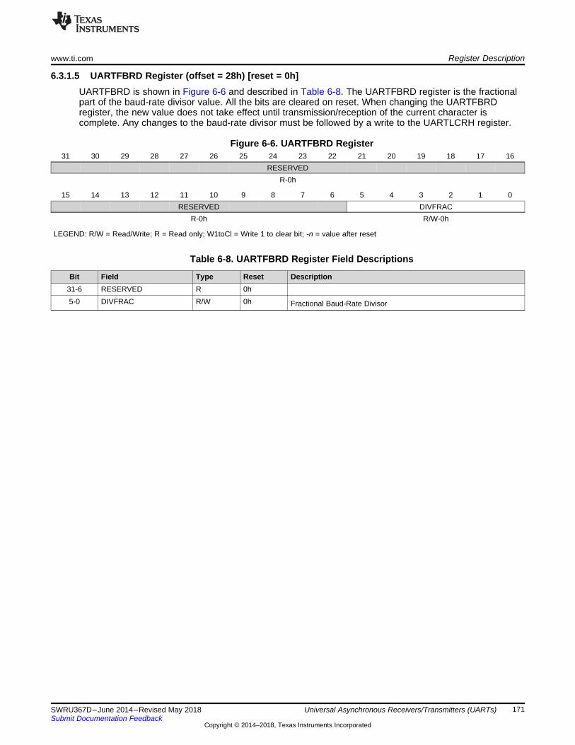
www.ti.com Register Description
171SWRU367D–June 2014–Revised May 2018Submit Documentation Feedback
Copyright © 2014–2018, Texas Instruments Incorporated
Universal Asynchronous Receivers/Transmitters (UARTs)
6.3.1.5 UARTFBRD Register (offset = 28h) [reset = 0h]UARTFBRD is shown in Figure 6-6 and described in Table 6-8. The UARTFBRD register is the fractionalpart of the baud-rate divisor value. All the bits are cleared on reset. When changing the UARTFBRDregister, the new value does not take effect until transmission/reception of the current character iscomplete. Any changes to the baud-rate divisor must be followed by a write to the UARTLCRH register.
Figure 6-6. UARTFBRD Register31 30 29 28 27 26 25 24 23 22 21 20 19 18 17 16
RESERVEDR-0h
15 14 13 12 11 10 9 8 7 6 5 4 3 2 1 0RESERVED DIVFRAC
R-0h R/W-0h
LEGEND: R/W = Read/Write; R = Read only; W1toCl = Write 1 to clear bit; -n = value after reset
Table 6-8. UARTFBRD Register Field Descriptions
Bit Field Type Reset Description31-6 RESERVED R 0h5-0 DIVFRAC R/W 0h Fractional Baud-Rate Divisor
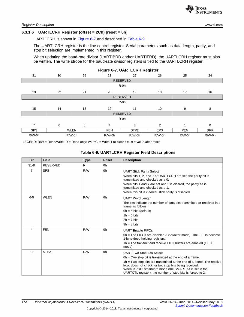
Register Description www.ti.com
172 SWRU367D–June 2014–Revised May 2018Submit Documentation Feedback
Copyright © 2014–2018, Texas Instruments Incorporated
Universal Asynchronous Receivers/Transmitters (UARTs)
6.3.1.6 UARTLCRH Register (offset = 2Ch) [reset = 0h]UARTLCRH is shown in Figure 6-7 and described in Table 6-9.
The UARTLCRH register is the line control register. Serial parameters such as data length, parity, andstop bit selection are implemented in this register.
When updating the baud-rate divisor (UARTIBRD and/or UARTIFRD), the UARTLCRH register must alsobe written. The write strobe for the baud-rate divisor registers is tied to the UARTLCRH register.
Figure 6-7. UARTLCRH Register31 30 29 28 27 26 25 24
RESERVEDR-0h
23 22 21 20 19 18 17 16RESERVED
R-0h
15 14 13 12 11 10 9 8RESERVED
R-0h
7 6 5 4 3 2 1 0SPS WLEN FEN STP2 EPS PEN BRK
R/W-0h R/W-0h R/W-0h R/W-0h R/W-0h R/W-0h R/W-0h
LEGEND: R/W = Read/Write; R = Read only; W1toCl = Write 1 to clear bit; -n = value after reset
Table 6-9. UARTLCRH Register Field Descriptions
Bit Field Type Reset Description31-8 RESERVED R 0h
7 SPS R/W 0h UART Stick Parity SelectWhen bits 1, 2, and 7 of UARTLCRH are set, the parity bit istransmitted and checked as a 0.When bits 1 and 7 are set and 2 is cleared, the parity bit istransmitted and checked as a 1.When this bit is cleared, stick parity is disabled.
6-5 WLEN R/W 0h UART Word LengthThe bits indicate the number of data bits transmitted or received in aframe as follows:0h = 5 bits (default)1h = 6 bits2h = 7 bits3h = 8 bits
4 FEN R/W 0h UART Enable FIFOs0h = The FIFOs are disabled (Character mode). The FIFOs become1-byte-deep holding registers.1h = The transmit and receive FIFO buffers are enabled (FIFOmode).
3 STP2 R/W 0h UART Two Stop Bits Select0h = One stop bit is transmitted at the end of a frame.1h = Two stop bits are transmitted at the end of a frame. The receivelogic does not check for two stop bits being received.When in 7816 smartcard mode (the SMART bit is set in theUARTCTL register), the number of stop bits is forced to 2.
www.ti.com Register Description
173SWRU367D–June 2014–Revised May 2018Submit Documentation Feedback
Copyright © 2014–2018, Texas Instruments Incorporated
Universal Asynchronous Receivers/Transmitters (UARTs)
Table 6-9. UARTLCRH Register Field Descriptions (continued)Bit Field Type Reset Description2 EPS R/W 0h UART Even Parity Select
0h = Odd parity is performed, which checks for an odd number of 1s.1h = Even parity generation and checking is performed duringtransmission and reception, which checks for an even number of 1sin data and parity bits.This bit has no effect when parity is disabled by the PEN bit.
1 PEN R/W 0h UART Parity Enable0h = Parity is disabled and no parity bit is added to the data frame.1h = Parity checking and generation is enabled.
0 BRK R/W 0h UART Send BreakA low level is continually output on the UnTx signal, after completingtransmission of the current character. For the proper execution of thebreak command, software must set this bit for at least two frames(character periods).
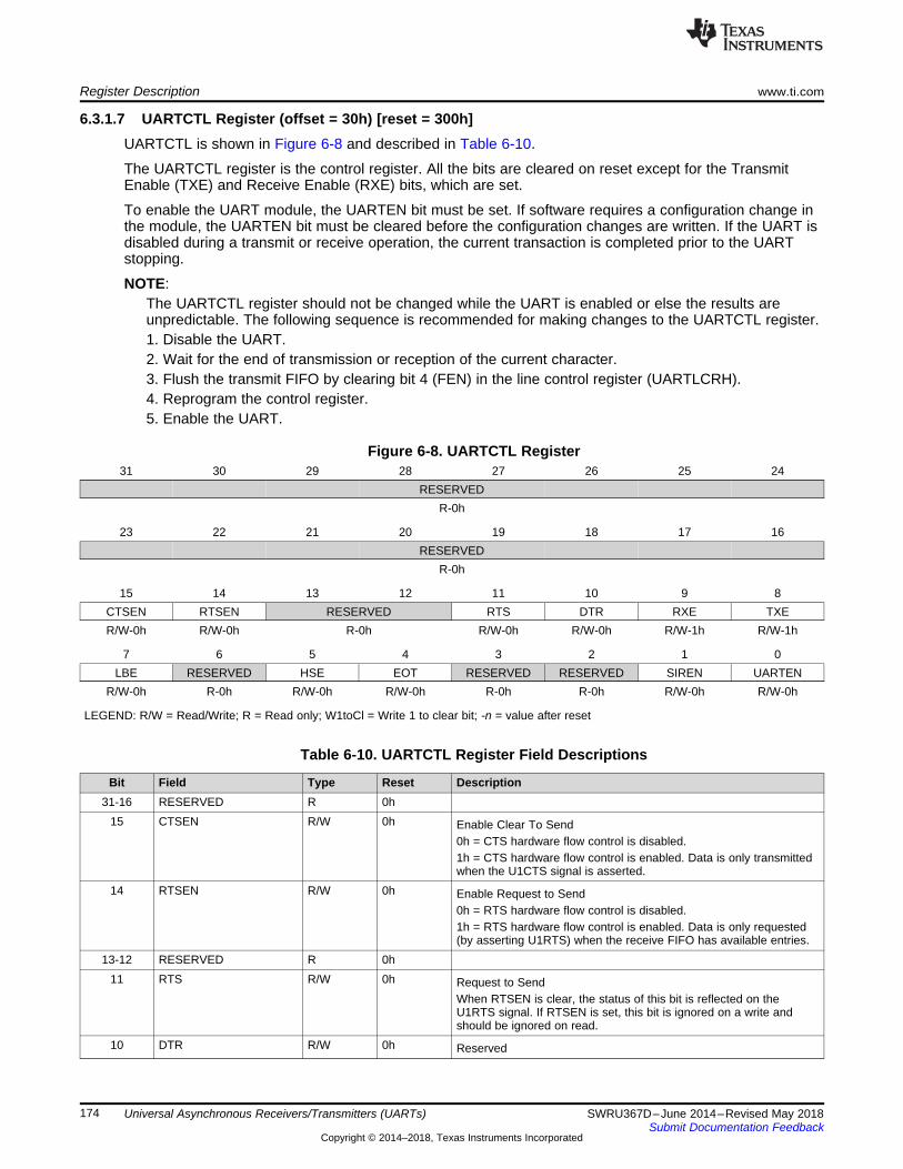
Register Description www.ti.com
174 SWRU367D–June 2014–Revised May 2018Submit Documentation Feedback
Copyright © 2014–2018, Texas Instruments Incorporated
Universal Asynchronous Receivers/Transmitters (UARTs)
6.3.1.7 UARTCTL Register (offset = 30h) [reset = 300h]UARTCTL is shown in Figure 6-8 and described in Table 6-10.
The UARTCTL register is the control register. All the bits are cleared on reset except for the TransmitEnable (TXE) and Receive Enable (RXE) bits, which are set.
To enable the UART module, the UARTEN bit must be set. If software requires a configuration change inthe module, the UARTEN bit must be cleared before the configuration changes are written. If the UART isdisabled during a transmit or receive operation, the current transaction is completed prior to the UARTstopping.
NOTE:The UARTCTL register should not be changed while the UART is enabled or else the results areunpredictable. The following sequence is recommended for making changes to the UARTCTL register.1. Disable the UART.2. Wait for the end of transmission or reception of the current character.3. Flush the transmit FIFO by clearing bit 4 (FEN) in the line control register (UARTLCRH).4. Reprogram the control register.5. Enable the UART.
Figure 6-8. UARTCTL Register31 30 29 28 27 26 25 24
RESERVEDR-0h
23 22 21 20 19 18 17 16RESERVED
R-0h
15 14 13 12 11 10 9 8CTSEN RTSEN RESERVED RTS DTR RXE TXER/W-0h R/W-0h R-0h R/W-0h R/W-0h R/W-1h R/W-1h
7 6 5 4 3 2 1 0LBE RESERVED HSE EOT RESERVED RESERVED SIREN UARTEN
R/W-0h R-0h R/W-0h R/W-0h R-0h R-0h R/W-0h R/W-0h
LEGEND: R/W = Read/Write; R = Read only; W1toCl = Write 1 to clear bit; -n = value after reset
Table 6-10. UARTCTL Register Field Descriptions
Bit Field Type Reset Description31-16 RESERVED R 0h
15 CTSEN R/W 0h Enable Clear To Send0h = CTS hardware flow control is disabled.1h = CTS hardware flow control is enabled. Data is only transmittedwhen the U1CTS signal is asserted.
14 RTSEN R/W 0h Enable Request to Send0h = RTS hardware flow control is disabled.1h = RTS hardware flow control is enabled. Data is only requested(by asserting U1RTS) when the receive FIFO has available entries.
13-12 RESERVED R 0h11 RTS R/W 0h Request to Send
When RTSEN is clear, the status of this bit is reflected on theU1RTS signal. If RTSEN is set, this bit is ignored on a write andshould be ignored on read.
10 DTR R/W 0h Reserved
www.ti.com Register Description
175SWRU367D–June 2014–Revised May 2018Submit Documentation Feedback
Copyright © 2014–2018, Texas Instruments Incorporated
Universal Asynchronous Receivers/Transmitters (UARTs)
Table 6-10. UARTCTL Register Field Descriptions (continued)Bit Field Type Reset Description9 RXE R/W 1h UART Receive Enable
0h = The receive section of the UART is disabled.1h = The receive section of the UART is enabled. If the UART isdisabled in the middle of a receive, it completes the currentcharacter before stopping.Note: To enable reception, the UARTEN bit must also be set.
8 TXE R/W 1h UART Transmit Enable0h = The transmit section of the UART is disabled.1h = The transmit section of the UART is enabled.If the UART is disabled in the middle of a transmission, it completesthe current character before stopping.Note: To enable transmission, the UARTEN bit must also be set.
7 LBE R/W 0h UART Loop Back Enable0h = Normal operation.1h = The UnTx path is fed through the UnRx path.
6 RESERVED R 0h5 HSE R/W 0h High-Speed Enable
0h = The UART is clocked using the system clock divided by 16.1h = The UART is clocked using the system clock divided by 8.Note: System clock used is also dependent on the baud-rate divisorconfiguration. The state of this bit has no effect on clock generationin ISO 7816 smart card mode (the SMART bit is set).
4 EOT R/W 0h End of TransmissionThis bit determines the behavior of the TXRIS bit in the UARTRISregister.0h = The TXRIS bit is set when the transmit FIFO condition specifiedin UARTIFLS is met.1h = The TXRIS bit is set only after all transmitted data, includingstop bits, have cleared the serializer.
3 RESERVED R 0h2 RESERVED R 0h1 SIREN R/W 0h RESERVED0 UARTEN R/W 0h UART Enable
0h = The UART is disabled.1h = The UART is enabled.If the UART is disabled in the middle of transmission or reception, itcompletes the current character before stopping.
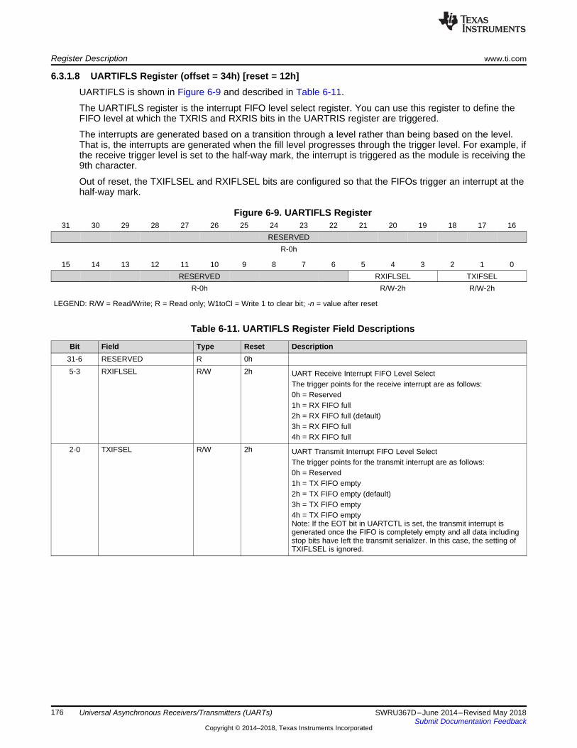
Register Description www.ti.com
176 SWRU367D–June 2014–Revised May 2018Submit Documentation Feedback
Copyright © 2014–2018, Texas Instruments Incorporated
Universal Asynchronous Receivers/Transmitters (UARTs)
6.3.1.8 UARTIFLS Register (offset = 34h) [reset = 12h]UARTIFLS is shown in Figure 6-9 and described in Table 6-11.
The UARTIFLS register is the interrupt FIFO level select register. You can use this register to define theFIFO level at which the TXRIS and RXRIS bits in the UARTRIS register are triggered.
The interrupts are generated based on a transition through a level rather than being based on the level.That is, the interrupts are generated when the fill level progresses through the trigger level. For example, ifthe receive trigger level is set to the half-way mark, the interrupt is triggered as the module is receiving the9th character.
Out of reset, the TXIFLSEL and RXIFLSEL bits are configured so that the FIFOs trigger an interrupt at thehalf-way mark.
Figure 6-9. UARTIFLS Register31 30 29 28 27 26 25 24 23 22 21 20 19 18 17 16
RESERVEDR-0h
15 14 13 12 11 10 9 8 7 6 5 4 3 2 1 0RESERVED RXIFLSEL TXIFSEL
R-0h R/W-2h R/W-2h
LEGEND: R/W = Read/Write; R = Read only; W1toCl = Write 1 to clear bit; -n = value after reset
Table 6-11. UARTIFLS Register Field Descriptions
Bit Field Type Reset Description31-6 RESERVED R 0h5-3 RXIFLSEL R/W 2h UART Receive Interrupt FIFO Level Select
The trigger points for the receive interrupt are as follows:0h = Reserved1h = RX FIFO full2h = RX FIFO full (default)3h = RX FIFO full4h = RX FIFO full
2-0 TXIFSEL R/W 2h UART Transmit Interrupt FIFO Level SelectThe trigger points for the transmit interrupt are as follows:0h = Reserved1h = TX FIFO empty2h = TX FIFO empty (default)3h = TX FIFO empty4h = TX FIFO emptyNote: If the EOT bit in UARTCTL is set, the transmit interrupt isgenerated once the FIFO is completely empty and all data includingstop bits have left the transmit serializer. In this case, the setting ofTXIFLSEL is ignored.
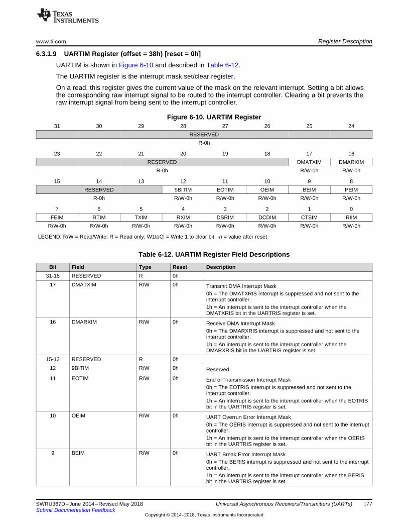
www.ti.com Register Description
177SWRU367D–June 2014–Revised May 2018Submit Documentation Feedback
Copyright © 2014–2018, Texas Instruments Incorporated
Universal Asynchronous Receivers/Transmitters (UARTs)
6.3.1.9 UARTIM Register (offset = 38h) [reset = 0h]UARTIM is shown in Figure 6-10 and described in Table 6-12.
The UARTIM register is the interrupt mask set/clear register.
On a read, this register gives the current value of the mask on the relevant interrupt. Setting a bit allowsthe corresponding raw interrupt signal to be routed to the interrupt controller. Clearing a bit prevents theraw interrupt signal from being sent to the interrupt controller.
Figure 6-10. UARTIM Register31 30 29 28 27 26 25 24
RESERVEDR-0h
23 22 21 20 19 18 17 16RESERVED DMATXIM DMARXIM
R-0h R/W-0h R/W-0h
15 14 13 12 11 10 9 8RESERVED 9BITIM EOTIM OEIM BEIM PEIM
R-0h R/W-0h R/W-0h R/W-0h R/W-0h R/W-0h
7 6 5 4 3 2 1 0FEIM RTIM TXIM RXIM DSRIM DCDIM CTSIM RIIM
R/W-0h R/W-0h R/W-0h R/W-0h R/W-0h R/W-0h R/W-0h R/W-0h
LEGEND: R/W = Read/Write; R = Read only; W1toCl = Write 1 to clear bit; -n = value after reset
Table 6-12. UARTIM Register Field Descriptions
Bit Field Type Reset Description31-18 RESERVED R 0h
17 DMATXIM R/W 0h Transmit DMA Interrupt Mask0h = The DMATXRIS interrupt is suppressed and not sent to theinterrupt controller.1h = An interrupt is sent to the interrupt controller when theDMATXRIS bit in the UARTRIS register is set.
16 DMARXIM R/W 0h Receive DMA Interrupt Mask0h = The DMARXRIS interrupt is suppressed and not sent to theinterrupt controller.1h = An interrupt is sent to the interrupt controller when theDMARXRIS bit in the UARTRIS register is set.
15-13 RESERVED R 0h12 9BITIM R/W 0h Reserved11 EOTIM R/W 0h End of Transmission Interrupt Mask
0h = The EOTRIS interrupt is suppressed and not sent to theinterrupt controller.1h = An interrupt is sent to the interrupt controller when the EOTRISbit in the UARTRIS register is set.
10 OEIM R/W 0h UART Overrun Error Interrupt Mask0h = The OERIS interrupt is suppressed and not sent to the interruptcontroller.1h = An interrupt is sent to the interrupt controller when the OERISbit in the UARTRIS register is set.
9 BEIM R/W 0h UART Break Error Interrupt Mask0h = The BERIS interrupt is suppressed and not sent to the interruptcontroller.1h = An interrupt is sent to the interrupt controller when the BERISbit in the UARTRIS register is set.
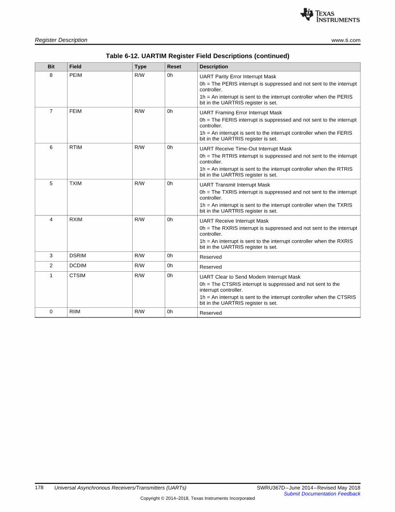
Register Description www.ti.com
178 SWRU367D–June 2014–Revised May 2018Submit Documentation Feedback
Copyright © 2014–2018, Texas Instruments Incorporated
Universal Asynchronous Receivers/Transmitters (UARTs)
Table 6-12. UARTIM Register Field Descriptions (continued)Bit Field Type Reset Description8 PEIM R/W 0h UART Parity Error Interrupt Mask
0h = The PERIS interrupt is suppressed and not sent to the interruptcontroller.1h = An interrupt is sent to the interrupt controller when the PERISbit in the UARTRIS register is set.
7 FEIM R/W 0h UART Framing Error Interrupt Mask0h = The FERIS interrupt is suppressed and not sent to the interruptcontroller.1h = An interrupt is sent to the interrupt controller when the FERISbit in the UARTRIS register is set.
6 RTIM R/W 0h UART Receive Time-Out Interrupt Mask0h = The RTRIS interrupt is suppressed and not sent to the interruptcontroller.1h = An interrupt is sent to the interrupt controller when the RTRISbit in the UARTRIS register is set.
5 TXIM R/W 0h UART Transmit Interrupt Mask0h = The TXRIS interrupt is suppressed and not sent to the interruptcontroller.1h = An interrupt is sent to the interrupt controller when the TXRISbit in the UARTRIS register is set.
4 RXIM R/W 0h UART Receive Interrupt Mask0h = The RXRIS interrupt is suppressed and not sent to the interruptcontroller.1h = An interrupt is sent to the interrupt controller when the RXRISbit in the UARTRIS register is set.
3 DSRIM R/W 0h Reserved2 DCDIM R/W 0h Reserved1 CTSIM R/W 0h UART Clear to Send Modem Interrupt Mask
0h = The CTSRIS interrupt is suppressed and not sent to theinterrupt controller.1h = An interrupt is sent to the interrupt controller when the CTSRISbit in the UARTRIS register is set.
0 RIIM R/W 0h Reserved
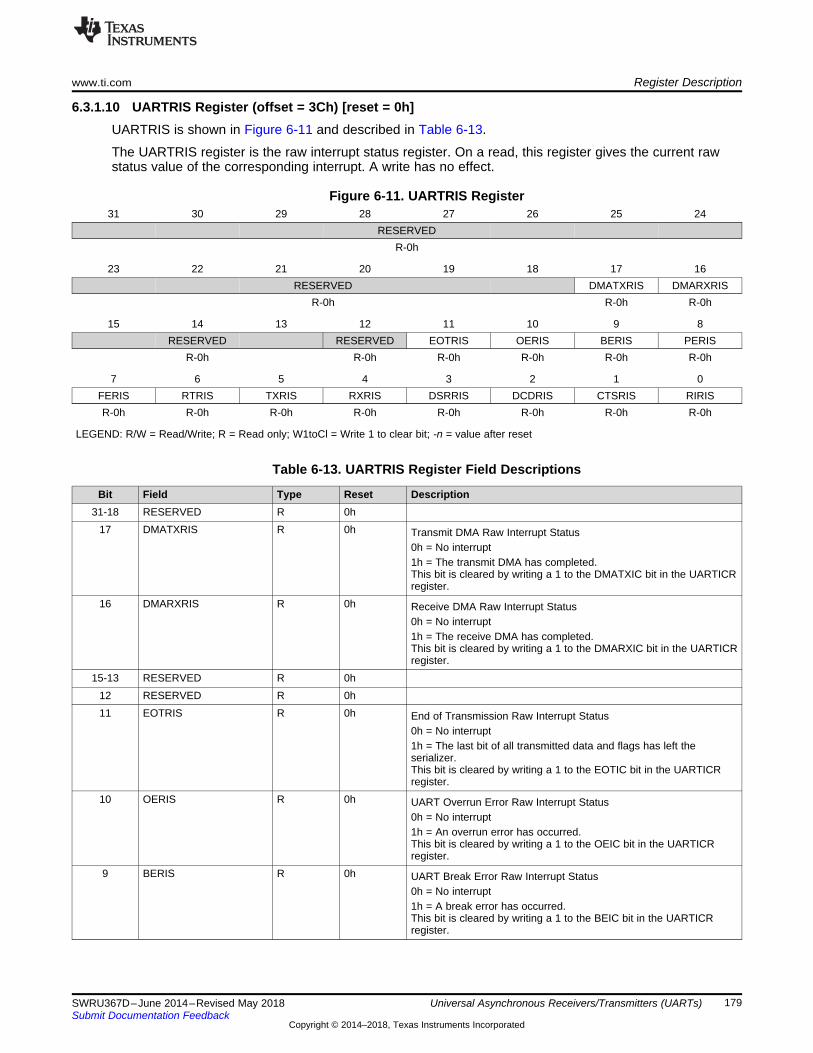
www.ti.com Register Description
179SWRU367D–June 2014–Revised May 2018Submit Documentation Feedback
Copyright © 2014–2018, Texas Instruments Incorporated
Universal Asynchronous Receivers/Transmitters (UARTs)
6.3.1.10 UARTRIS Register (offset = 3Ch) [reset = 0h]UARTRIS is shown in Figure 6-11 and described in Table 6-13.
The UARTRIS register is the raw interrupt status register. On a read, this register gives the current rawstatus value of the corresponding interrupt. A write has no effect.
Figure 6-11. UARTRIS Register31 30 29 28 27 26 25 24
RESERVEDR-0h
23 22 21 20 19 18 17 16RESERVED DMATXRIS DMARXRIS
R-0h R-0h R-0h
15 14 13 12 11 10 9 8RESERVED RESERVED EOTRIS OERIS BERIS PERIS
R-0h R-0h R-0h R-0h R-0h R-0h
7 6 5 4 3 2 1 0FERIS RTRIS TXRIS RXRIS DSRRIS DCDRIS CTSRIS RIRISR-0h R-0h R-0h R-0h R-0h R-0h R-0h R-0h
LEGEND: R/W = Read/Write; R = Read only; W1toCl = Write 1 to clear bit; -n = value after reset
Table 6-13. UARTRIS Register Field Descriptions
Bit Field Type Reset Description31-18 RESERVED R 0h
17 DMATXRIS R 0h Transmit DMA Raw Interrupt Status0h = No interrupt1h = The transmit DMA has completed.This bit is cleared by writing a 1 to the DMATXIC bit in the UARTICRregister.
16 DMARXRIS R 0h Receive DMA Raw Interrupt Status0h = No interrupt1h = The receive DMA has completed.This bit is cleared by writing a 1 to the DMARXIC bit in the UARTICRregister.
15-13 RESERVED R 0h12 RESERVED R 0h11 EOTRIS R 0h End of Transmission Raw Interrupt Status
0h = No interrupt1h = The last bit of all transmitted data and flags has left theserializer.This bit is cleared by writing a 1 to the EOTIC bit in the UARTICRregister.
10 OERIS R 0h UART Overrun Error Raw Interrupt Status0h = No interrupt1h = An overrun error has occurred.This bit is cleared by writing a 1 to the OEIC bit in the UARTICRregister.
9 BERIS R 0h UART Break Error Raw Interrupt Status0h = No interrupt1h = A break error has occurred.This bit is cleared by writing a 1 to the BEIC bit in the UARTICRregister.
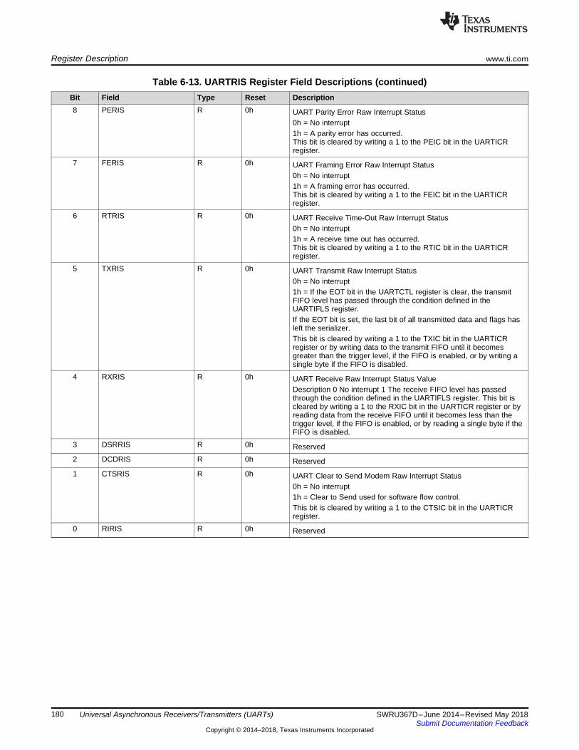
Register Description www.ti.com
180 SWRU367D–June 2014–Revised May 2018Submit Documentation Feedback
Copyright © 2014–2018, Texas Instruments Incorporated
Universal Asynchronous Receivers/Transmitters (UARTs)
Table 6-13. UARTRIS Register Field Descriptions (continued)Bit Field Type Reset Description8 PERIS R 0h UART Parity Error Raw Interrupt Status
0h = No interrupt1h = A parity error has occurred.This bit is cleared by writing a 1 to the PEIC bit in the UARTICRregister.
7 FERIS R 0h UART Framing Error Raw Interrupt Status0h = No interrupt1h = A framing error has occurred.This bit is cleared by writing a 1 to the FEIC bit in the UARTICRregister.
6 RTRIS R 0h UART Receive Time-Out Raw Interrupt Status0h = No interrupt1h = A receive time out has occurred.This bit is cleared by writing a 1 to the RTIC bit in the UARTICRregister.
5 TXRIS R 0h UART Transmit Raw Interrupt Status0h = No interrupt1h = If the EOT bit in the UARTCTL register is clear, the transmitFIFO level has passed through the condition defined in theUARTIFLS register.If the EOT bit is set, the last bit of all transmitted data and flags hasleft the serializer.This bit is cleared by writing a 1 to the TXIC bit in the UARTICRregister or by writing data to the transmit FIFO until it becomesgreater than the trigger level, if the FIFO is enabled, or by writing asingle byte if the FIFO is disabled.
4 RXRIS R 0h UART Receive Raw Interrupt Status ValueDescription 0 No interrupt 1 The receive FIFO level has passedthrough the condition defined in the UARTIFLS register. This bit iscleared by writing a 1 to the RXIC bit in the UARTICR register or byreading data from the receive FIFO until it becomes less than thetrigger level, if the FIFO is enabled, or by reading a single byte if theFIFO is disabled.
3 DSRRIS R 0h Reserved2 DCDRIS R 0h Reserved1 CTSRIS R 0h UART Clear to Send Modem Raw Interrupt Status
0h = No interrupt1h = Clear to Send used for software flow control.This bit is cleared by writing a 1 to the CTSIC bit in the UARTICRregister.
0 RIRIS R 0h Reserved
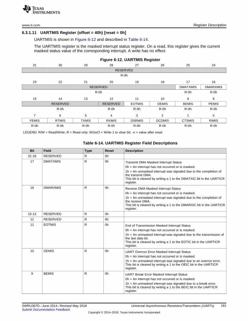
www.ti.com Register Description
181SWRU367D–June 2014–Revised May 2018Submit Documentation Feedback
Copyright © 2014–2018, Texas Instruments Incorporated
Universal Asynchronous Receivers/Transmitters (UARTs)
6.3.1.11 UARTMIS Register (offset = 40h) [reset = 0h]UARTMIS is shown in Figure 6-12 and described in Table 6-14.
The UARTMIS register is the masked interrupt status register. On a read, this register gives the currentmasked status value of the corresponding interrupt. A write has no effect.
Figure 6-12. UARTMIS Register31 30 29 28 27 26 25 24
RESERVEDR-0h
23 22 21 20 19 18 17 16RESERVED DMATXMIS DMARXMIS
R-0h R-0h R-0h
15 14 13 12 11 10 9 8RESERVED RESERVED EOTMIS OEMIS BEMIS PEMIS
R-0h R-0h R-0h R-0h R-0h R-0h
7 6 5 4 3 2 1 0FEMIS RTMIS TXMIS RXMIS DSRMIS DCDMIS CTSMIS RIMISR-0h R-0h R-0h R-0h R-0h R-0h R-0h R-0h
LEGEND: R/W = Read/Write; R = Read only; W1toCl = Write 1 to clear bit; -n = value after reset
Table 6-14. UARTMIS Register Field Descriptions
Bit Field Type Reset Description31-18 RESERVED R 0h
17 DMATXMIS R 0h Transmit DMA Masked Interrupt Status0h = An interrupt has not occurred or is masked.1h = An unmasked interrupt was signaled due to the completion ofthe transmit DMA.This bit is cleared by writing a 1 to the DMATXIC bit in the UARTICRregister.
16 DMARXMIS R 0h Receive DMA Masked Interrupt Status0h = An interrupt has not occurred or is masked.1h = An unmasked interrupt was signaled due to the completion ofthe receive DMA.This bit is cleared by writing a 1 to the DMARXIC bit in the UARTICRregister.
15-13 RESERVED R 0h12 RESERVED R 0h11 EOTMIS R 0h End of Transmission Masked Interrupt Status
0h = An interrupt has not occurred or is masked.1h = An unmasked interrupt was signaled due to the transmission ofthe last data bit.This bit is cleared by writing a 1 to the EOTIC bit in the UARTICRregister.
10 OEMIS R 0h UART Overrun Error Masked Interrupt Status0h = An interrupt has not occurred or is masked.1h = An unmasked interrupt was signaled due to an overrun error.This bit is cleared by writing a 1 to the OEIC bit in the UARTICRregister.
9 BEMIS R 0h UART Break Error Masked Interrupt Status0h = An interrupt has not occurred or is masked.1h = An unmasked interrupt was signaled due to a break error.This bit is cleared by writing a 1 to the BEIC bit in the UARTICRregister.
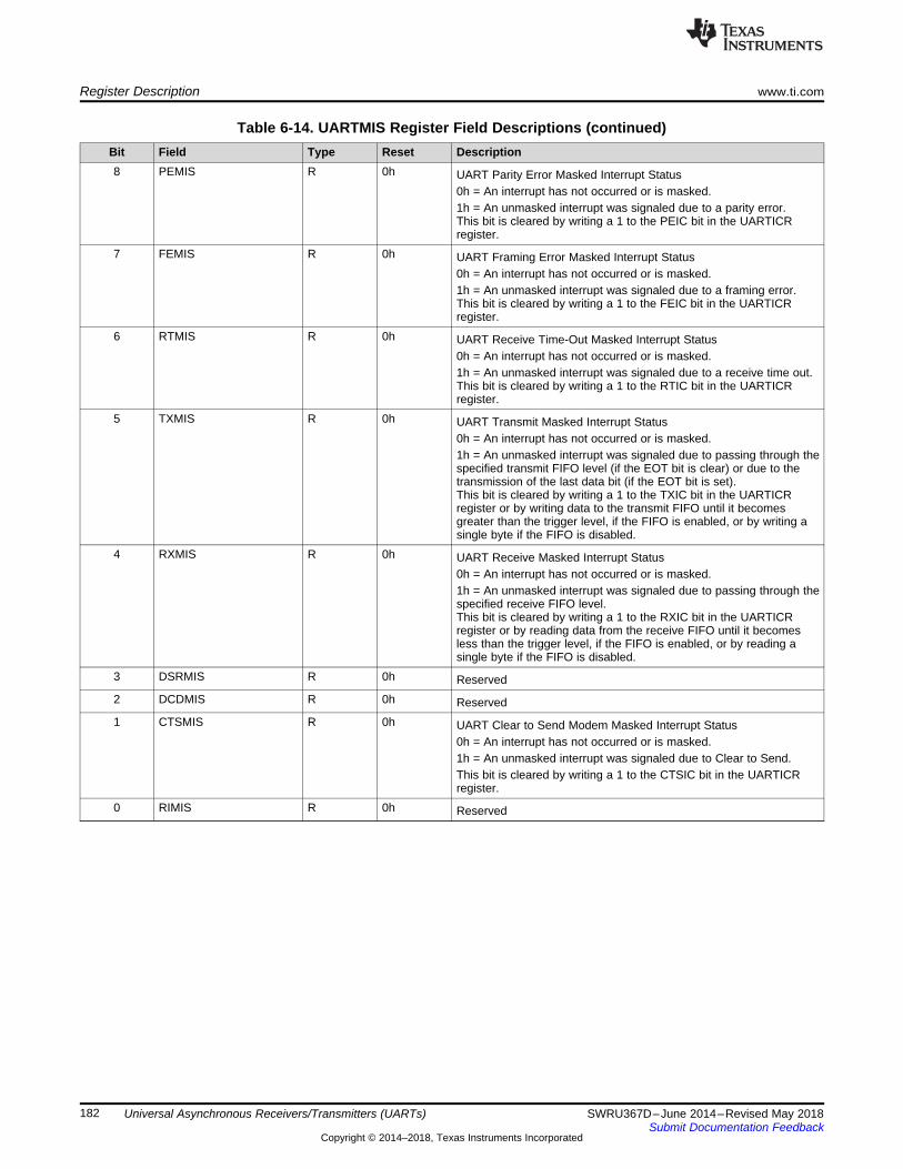
Register Description www.ti.com
182 SWRU367D–June 2014–Revised May 2018Submit Documentation Feedback
Copyright © 2014–2018, Texas Instruments Incorporated
Universal Asynchronous Receivers/Transmitters (UARTs)
Table 6-14. UARTMIS Register Field Descriptions (continued)Bit Field Type Reset Description8 PEMIS R 0h UART Parity Error Masked Interrupt Status
0h = An interrupt has not occurred or is masked.1h = An unmasked interrupt was signaled due to a parity error.This bit is cleared by writing a 1 to the PEIC bit in the UARTICRregister.
7 FEMIS R 0h UART Framing Error Masked Interrupt Status0h = An interrupt has not occurred or is masked.1h = An unmasked interrupt was signaled due to a framing error.This bit is cleared by writing a 1 to the FEIC bit in the UARTICRregister.
6 RTMIS R 0h UART Receive Time-Out Masked Interrupt Status0h = An interrupt has not occurred or is masked.1h = An unmasked interrupt was signaled due to a receive time out.This bit is cleared by writing a 1 to the RTIC bit in the UARTICRregister.
5 TXMIS R 0h UART Transmit Masked Interrupt Status0h = An interrupt has not occurred or is masked.1h = An unmasked interrupt was signaled due to passing through thespecified transmit FIFO level (if the EOT bit is clear) or due to thetransmission of the last data bit (if the EOT bit is set).This bit is cleared by writing a 1 to the TXIC bit in the UARTICRregister or by writing data to the transmit FIFO until it becomesgreater than the trigger level, if the FIFO is enabled, or by writing asingle byte if the FIFO is disabled.
4 RXMIS R 0h UART Receive Masked Interrupt Status0h = An interrupt has not occurred or is masked.1h = An unmasked interrupt was signaled due to passing through thespecified receive FIFO level.This bit is cleared by writing a 1 to the RXIC bit in the UARTICRregister or by reading data from the receive FIFO until it becomesless than the trigger level, if the FIFO is enabled, or by reading asingle byte if the FIFO is disabled.
3 DSRMIS R 0h Reserved2 DCDMIS R 0h Reserved1 CTSMIS R 0h UART Clear to Send Modem Masked Interrupt Status
0h = An interrupt has not occurred or is masked.1h = An unmasked interrupt was signaled due to Clear to Send.This bit is cleared by writing a 1 to the CTSIC bit in the UARTICRregister.
0 RIMIS R 0h Reserved
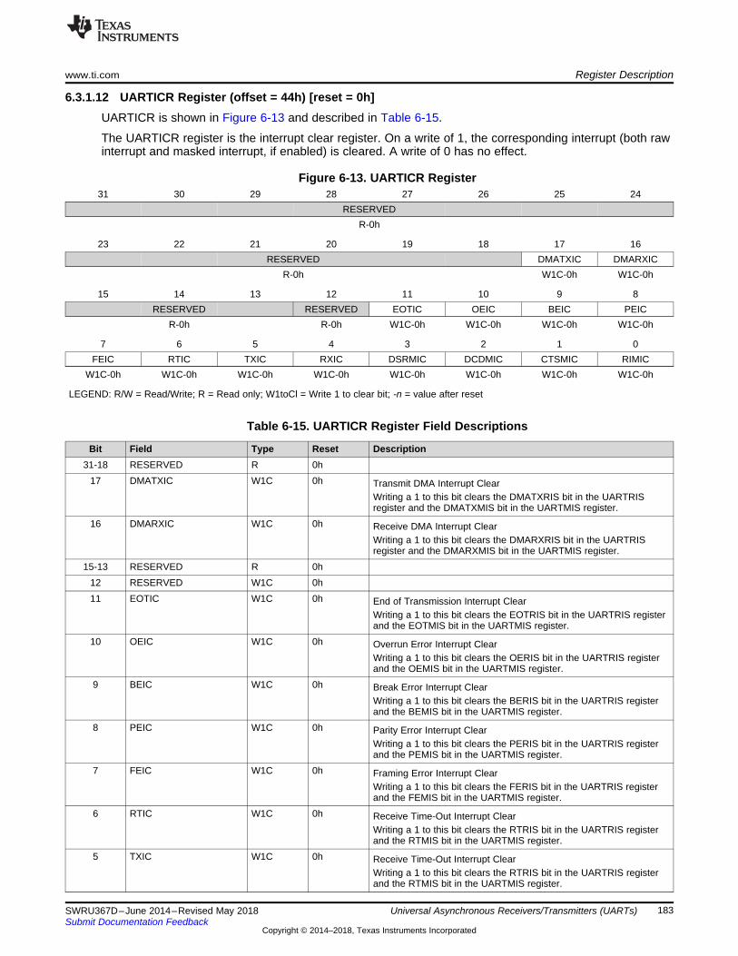
www.ti.com Register Description
183SWRU367D–June 2014–Revised May 2018Submit Documentation Feedback
Copyright © 2014–2018, Texas Instruments Incorporated
Universal Asynchronous Receivers/Transmitters (UARTs)
6.3.1.12 UARTICR Register (offset = 44h) [reset = 0h]UARTICR is shown in Figure 6-13 and described in Table 6-15.
The UARTICR register is the interrupt clear register. On a write of 1, the corresponding interrupt (both rawinterrupt and masked interrupt, if enabled) is cleared. A write of 0 has no effect.
Figure 6-13. UARTICR Register31 30 29 28 27 26 25 24
RESERVEDR-0h
23 22 21 20 19 18 17 16RESERVED DMATXIC DMARXIC
R-0h W1C-0h W1C-0h
15 14 13 12 11 10 9 8RESERVED RESERVED EOTIC OEIC BEIC PEIC
R-0h R-0h W1C-0h W1C-0h W1C-0h W1C-0h
7 6 5 4 3 2 1 0FEIC RTIC TXIC RXIC DSRMIC DCDMIC CTSMIC RIMIC
W1C-0h W1C-0h W1C-0h W1C-0h W1C-0h W1C-0h W1C-0h W1C-0h
LEGEND: R/W = Read/Write; R = Read only; W1toCl = Write 1 to clear bit; -n = value after reset
Table 6-15. UARTICR Register Field Descriptions
Bit Field Type Reset Description31-18 RESERVED R 0h
17 DMATXIC W1C 0h Transmit DMA Interrupt ClearWriting a 1 to this bit clears the DMATXRIS bit in the UARTRISregister and the DMATXMIS bit in the UARTMIS register.
16 DMARXIC W1C 0h Receive DMA Interrupt ClearWriting a 1 to this bit clears the DMARXRIS bit in the UARTRISregister and the DMARXMIS bit in the UARTMIS register.
15-13 RESERVED R 0h12 RESERVED W1C 0h11 EOTIC W1C 0h End of Transmission Interrupt Clear
Writing a 1 to this bit clears the EOTRIS bit in the UARTRIS registerand the EOTMIS bit in the UARTMIS register.
10 OEIC W1C 0h Overrun Error Interrupt ClearWriting a 1 to this bit clears the OERIS bit in the UARTRIS registerand the OEMIS bit in the UARTMIS register.
9 BEIC W1C 0h Break Error Interrupt ClearWriting a 1 to this bit clears the BERIS bit in the UARTRIS registerand the BEMIS bit in the UARTMIS register.
8 PEIC W1C 0h Parity Error Interrupt ClearWriting a 1 to this bit clears the PERIS bit in the UARTRIS registerand the PEMIS bit in the UARTMIS register.
7 FEIC W1C 0h Framing Error Interrupt ClearWriting a 1 to this bit clears the FERIS bit in the UARTRIS registerand the FEMIS bit in the UARTMIS register.
6 RTIC W1C 0h Receive Time-Out Interrupt ClearWriting a 1 to this bit clears the RTRIS bit in the UARTRIS registerand the RTMIS bit in the UARTMIS register.
5 TXIC W1C 0h Receive Time-Out Interrupt ClearWriting a 1 to this bit clears the RTRIS bit in the UARTRIS registerand the RTMIS bit in the UARTMIS register.
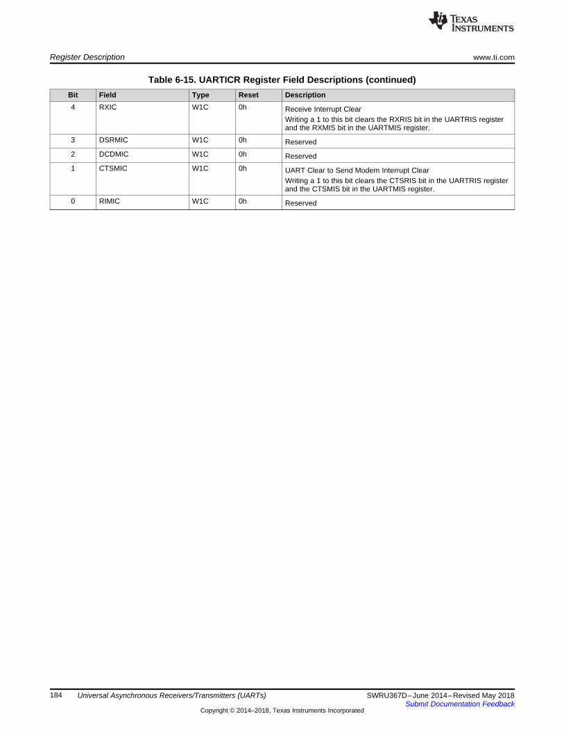
Register Description www.ti.com
184 SWRU367D–June 2014–Revised May 2018Submit Documentation Feedback
Copyright © 2014–2018, Texas Instruments Incorporated
Universal Asynchronous Receivers/Transmitters (UARTs)
Table 6-15. UARTICR Register Field Descriptions (continued)Bit Field Type Reset Description4 RXIC W1C 0h Receive Interrupt Clear
Writing a 1 to this bit clears the RXRIS bit in the UARTRIS registerand the RXMIS bit in the UARTMIS register.
3 DSRMIC W1C 0h Reserved2 DCDMIC W1C 0h Reserved1 CTSMIC W1C 0h UART Clear to Send Modem Interrupt Clear
Writing a 1 to this bit clears the CTSRIS bit in the UARTRIS registerand the CTSMIS bit in the UARTMIS register.
0 RIMIC W1C 0h Reserved
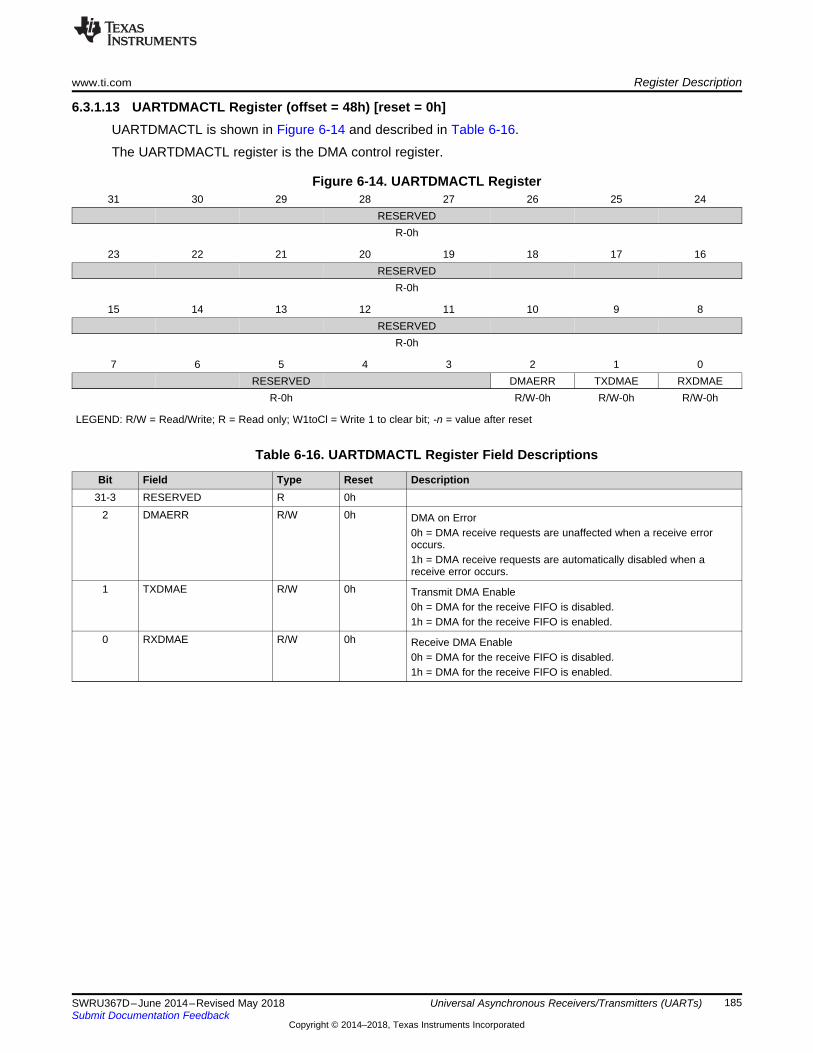
www.ti.com Register Description
185SWRU367D–June 2014–Revised May 2018Submit Documentation Feedback
Copyright © 2014–2018, Texas Instruments Incorporated
Universal Asynchronous Receivers/Transmitters (UARTs)
6.3.1.13 UARTDMACTL Register (offset = 48h) [reset = 0h]UARTDMACTL is shown in Figure 6-14 and described in Table 6-16.
The UARTDMACTL register is the DMA control register.
Figure 6-14. UARTDMACTL Register31 30 29 28 27 26 25 24
RESERVEDR-0h
23 22 21 20 19 18 17 16RESERVED
R-0h
15 14 13 12 11 10 9 8RESERVED
R-0h
7 6 5 4 3 2 1 0RESERVED DMAERR TXDMAE RXDMAE
R-0h R/W-0h R/W-0h R/W-0h
LEGEND: R/W = Read/Write; R = Read only; W1toCl = Write 1 to clear bit; -n = value after reset
Table 6-16. UARTDMACTL Register Field Descriptions
Bit Field Type Reset Description31-3 RESERVED R 0h
2 DMAERR R/W 0h DMA on Error0h = DMA receive requests are unaffected when a receive erroroccurs.1h = DMA receive requests are automatically disabled when areceive error occurs.
1 TXDMAE R/W 0h Transmit DMA Enable0h = DMA for the receive FIFO is disabled.1h = DMA for the receive FIFO is enabled.
0 RXDMAE R/W 0h Receive DMA Enable0h = DMA for the receive FIFO is disabled.1h = DMA for the receive FIFO is enabled.
186 SWRU367D–June 2014–Revised May 2018Submit Documentation Feedback
Copyright © 2014–2018, Texas Instruments Incorporated
Inter-Integrated Circuit (I2C) Interface
Chapter 7SWRU367D–June 2014–Revised May 2018
Inter-Integrated Circuit (I2C) Interface
Topic ........................................................................................................................... Page
7.1 Overview ......................................................................................................... 1877.2 Functional Description ...................................................................................... 1897.3 Register Map.................................................................................................... 204
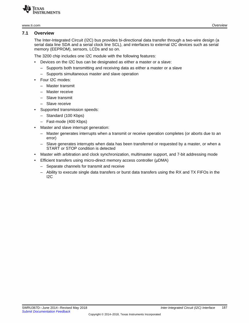
www.ti.com Overview
187SWRU367D–June 2014–Revised May 2018Submit Documentation Feedback
Copyright © 2014–2018, Texas Instruments Incorporated
Inter-Integrated Circuit (I2C) Interface
7.1 OverviewThe Inter-Integrated Circuit (I2C) bus provides bi-directional data transfer through a two-wire design (aserial data line SDA and a serial clock line SCL), and interfaces to external I2C devices such as serialmemory (EEPROM), sensors, LCDs and so on.
The 3200 chip includes one I2C module with the following features:• Devices on the I2C bus can be designated as either a master or a slave:
– Supports both transmitting and receiving data as either a master or a slave– Supports simultaneous master and slave operation
• Four I2C modes:– Master transmit– Master receive– Slave transmit– Slave receive
• Supported transmission speeds:– Standard (100 Kbps)– Fast-mode (400 Kbps)
• Master and slave interrupt generation:– Master generates interrupts when a transmit or receive operation completes (or aborts due to an
error)– Slave generates interrupts when data has been transferred or requested by a master, or when a
START or STOP condition is detected• Master with arbitration and clock synchronization, multimaster support, and 7-bit addressing mode• Efficient transfers using micro-direct memory access controller (µDMA)
– Separate channels for transmit and receive– Ability to execute single data transfers or burst data transfers using the RX and TX FIFOs in the
I2C
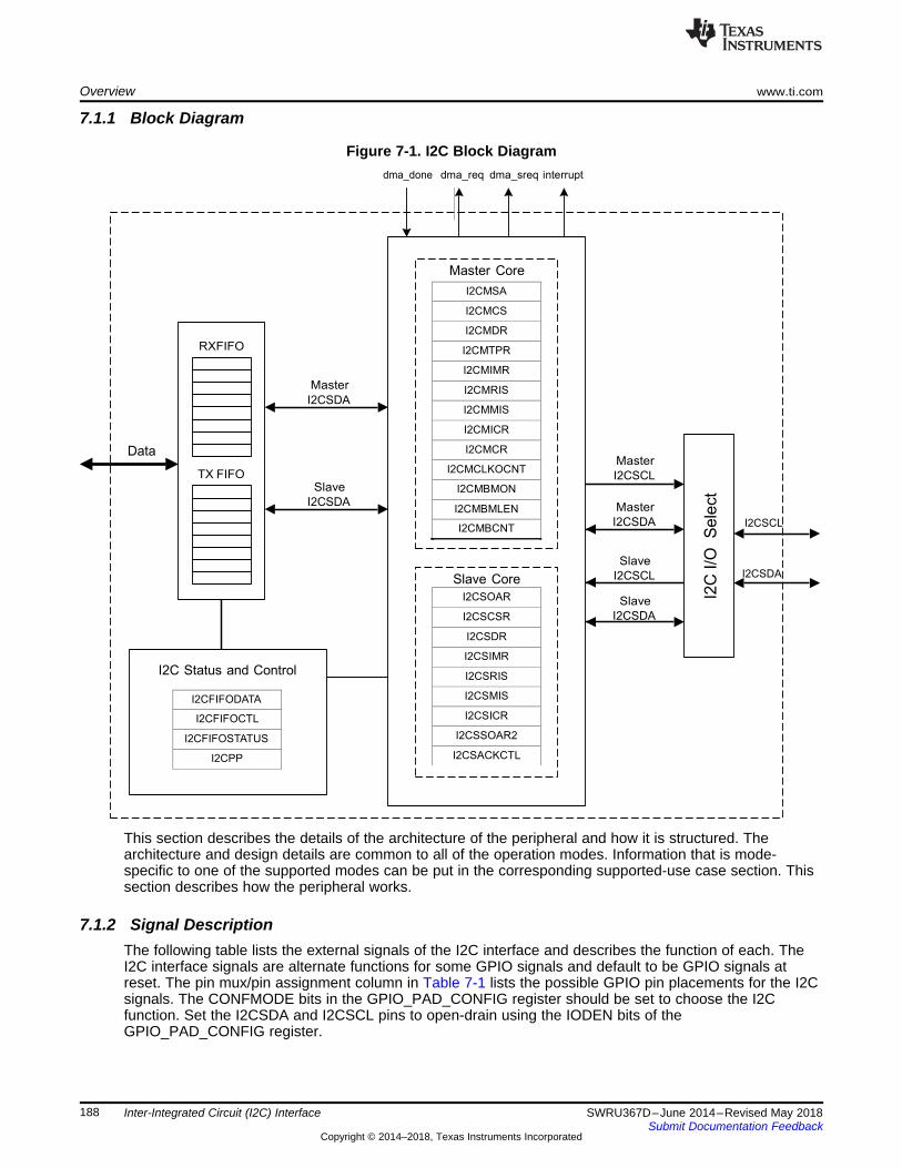
Overview www.ti.com
188 SWRU367D–June 2014–Revised May 2018Submit Documentation Feedback
Copyright © 2014–2018, Texas Instruments Incorporated
Inter-Integrated Circuit (I2C) Interface
7.1.1 Block Diagram
Figure 7-1. I2C Block Diagram
This section describes the details of the architecture of the peripheral and how it is structured. Thearchitecture and design details are common to all of the operation modes. Information that is mode-specific to one of the supported modes can be put in the corresponding supported-use case section. Thissection describes how the peripheral works.
7.1.2 Signal DescriptionThe following table lists the external signals of the I2C interface and describes the function of each. TheI2C interface signals are alternate functions for some GPIO signals and default to be GPIO signals atreset. The pin mux/pin assignment column in Table 7-1 lists the possible GPIO pin placements for the I2Csignals. The CONFMODE bits in the GPIO_PAD_CONFIG register should be set to choose the I2Cfunction. Set the I2CSDA and I2CSCL pins to open-drain using the IODEN bits of theGPIO_PAD_CONFIG register.
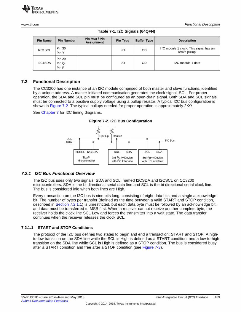
Rpullup Rpullup
I2CSCL I2CSDA
Tiva™Microcontroller
SCL SDA
3rd Party Device
with Interface
SCL SDA
3rd Party Device
SCLSDA
I C Bus2
I C2 with InterfaceI C2
••
••
••
••
www.ti.com Functional Description
189SWRU367D–June 2014–Revised May 2018Submit Documentation Feedback
Copyright © 2014–2018, Texas Instruments Incorporated
Inter-Integrated Circuit (I2C) Interface
Table 7-1. I2C Signals (64QFN)
Pin Name Pin Number Pin Mux / PinAssignment Pin Type Buffer Type Description
I2C1SCL Pin 30Pin Y
I/O OD I 2C module 1 clock. This signal has anactive pullup.
I2C1SDAPin 29Pin QPin R
I/O OD I2C module 1 data
7.2 Functional DescriptionThe CC3200 has one instance of an I2C module comprised of both master and slave functions, identifiedby a unique address. A master-initiated communication generates the clock signal, SCL. For properoperation, the SDA and SCL pin must be configured as an open-drain signal. Both SDA and SCL signalsmust be connected to a positive supply voltage using a pullup resistor. A typical I2C bus configuration isshown in Figure 7-2. The typical pullups needed for proper operation is approximately 2KΩ.
See Chapter 7 for I2C timing diagrams.
Figure 7-2. I2C Bus Configuration
7.2.1 I2C Bus Functional OverviewThe I2C bus uses only two signals: SDA and SCL, named I2CSDA and I2CSCL on CC3200microcontrollers. SDA is the bi-directional serial data line and SCL is the bi-directional serial clock line.The bus is considered idle when both lines are High.
Every transaction on the I2C bus is nine bits long, consisting of eight data bits and a single acknowledgebit. The number of bytes per transfer (defined as the time between a valid START and STOP condition,described in Section 7.2.1.1) is unrestricted, but each data byte must be followed by an acknowledge bit,and data must be transferred to MSB first. When a receiver cannot receive another complete byte, thereceiver holds the clock line SCL Low and forces the transmitter into a wait state. The data transfercontinues when the receiver releases the clock SCL.
7.2.1.1 START and STOP ConditionsThe protocol of the I2C bus defines two states to begin and end a transaction: START and STOP. A high-to-low transition on the SDA line while the SCL is High is defined as a START condition, and a low-to-hightransition on the SDA line while SCL is High is defined as a STOP condition. The bus is considered busyafter a START condition and free after a STOP condition (see Figure 7-3).
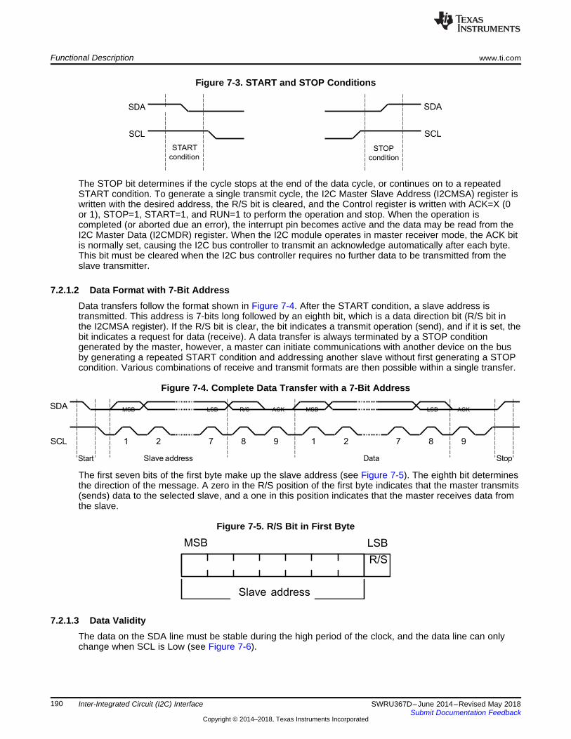
Functional Description www.ti.com
190 SWRU367D–June 2014–Revised May 2018Submit Documentation Feedback
Copyright © 2014–2018, Texas Instruments Incorporated
Inter-Integrated Circuit (I2C) Interface
Figure 7-3. START and STOP Conditions
The STOP bit determines if the cycle stops at the end of the data cycle, or continues on to a repeatedSTART condition. To generate a single transmit cycle, the I2C Master Slave Address (I2CMSA) register iswritten with the desired address, the R/S bit is cleared, and the Control register is written with ACK=X (0or 1), STOP=1, START=1, and RUN=1 to perform the operation and stop. When the operation iscompleted (or aborted due an error), the interrupt pin becomes active and the data may be read from theI2C Master Data (I2CMDR) register. When the I2C module operates in master receiver mode, the ACK bitis normally set, causing the I2C bus controller to transmit an acknowledge automatically after each byte.This bit must be cleared when the I2C bus controller requires no further data to be transmitted from theslave transmitter.
7.2.1.2 Data Format with 7-Bit AddressData transfers follow the format shown in Figure 7-4. After the START condition, a slave address istransmitted. This address is 7-bits long followed by an eighth bit, which is a data direction bit (R/S bit inthe I2CMSA register). If the R/S bit is clear, the bit indicates a transmit operation (send), and if it is set, thebit indicates a request for data (receive). A data transfer is always terminated by a STOP conditiongenerated by the master, however, a master can initiate communications with another device on the busby generating a repeated START condition and addressing another slave without first generating a STOPcondition. Various combinations of receive and transmit formats are then possible within a single transfer.
Figure 7-4. Complete Data Transfer with a 7-Bit Address
The first seven bits of the first byte make up the slave address (see Figure 7-5). The eighth bit determinesthe direction of the message. A zero in the R/S position of the first byte indicates that the master transmits(sends) data to the selected slave, and a one in this position indicates that the master receives data fromthe slave.
Figure 7-5. R/S Bit in First Byte
7.2.1.3 Data ValidityThe data on the SDA line must be stable during the high period of the clock, and the data line can onlychange when SCL is Low (see Figure 7-6).

www.ti.com Functional Description
191SWRU367D–June 2014–Revised May 2018Submit Documentation Feedback
Copyright © 2014–2018, Texas Instruments Incorporated
Inter-Integrated Circuit (I2C) Interface
Figure 7-6. Data Validity During Bit Transfer on the I2C Bus
7.2.1.4 AcknowledgeAll bus transactions have a required acknowledge clock cycle generated by the master. During theacknowledge cycle, the transmitter (which can be the master or slave) releases the SDA line. Toacknowledge the transaction, the receiver must pull down SDA during the acknowledge clock cycle. Thedata transmitted out by the receiver during the acknowledge cycle must comply with the data validityrequirements described in Section 7.2.1.3.
When a slave receiver does not acknowledge the slave address, SDA must be left High by the slave sothat the master can generate a STOP condition and abort the current transfer. If the master device isacting as a receiver during a transfer, it is responsible for acknowledging each transfer made by the slave.Because the master controls the number of bytes in the transfer, it signals the end of data to the slavetransmitter by not generating an acknowledge on the last data byte. The slave transmitter must thenrelease SDA to allow the master to generate the STOP or a repeated START condition.
If the slave is required to provide a manual ACK or NACK, the I2C Slave ACK Control (I2CSACKCTL)register allows the slave to NACK for invalid data or command or ACK for valid data or command. Whenthis operation is enabled, the MCU slave module I2C clock is pulled low after the last data bit, until thisregister is written with the indicated response.
7.2.1.5 Repeated StartThe I2C master module has the capability of executing a repeated START (transmit or receive) after aninitial transfer has occurred.
A repeated start sequence for a master transmit is as follows:1. When the device is in the idle state, the master writes the slave address to the I2CMSA register and
configures the R/S bit for the desired transfer type.2. Data is written to the I2CMDR register.3. When the BUSY bit in the I2CMCS register is 0, the master writes 0x3 to the I2CMCS register to
initiate a transfer.4. The master does not generate a STOP condition, but instead writes another slave address to the
I2CMSA register, then writes 0x3 to initiate the repeated START.
A repeated start sequence for a master receive is similar:1. When the device is in idle, the master writes the slave address to the I2CMSA register and configures
the R/S bit for the desired transfer type.2. The master reads data from the I2CMDR register.3. When the BUSY bit in the I2CMCS register is 0, the master writes 0x3 to the I2CMCS register to
initiate a transfer.4. The master does not generate a STOP condition, but instead writes another slave address to the
I2CMSA register, then writes 0x3 to initiate the repeated START.
Functional Description www.ti.com
192 SWRU367D–June 2014–Revised May 2018Submit Documentation Feedback
Copyright © 2014–2018, Texas Instruments Incorporated
Inter-Integrated Circuit (I2C) Interface
7.2.1.6 Clock Low Timeout (CLTO)The I2C slave can extend the transaction by periodically pulling the clock low to create a slow bit transferrate. The I2C module has a 12-bit programmable counter that tracks how long the clock has been heldlow. The upper 8 bits of the count value are software-programmable through the I2C Master Clock LowTimeout Count (I2CMCLKOCNT) register. The lower four bits are not user-visible, and are 0x0. The CNTLvalue programmed in the I2CMCLKOCNT register must be greater than 0x01. The application canprogram the eight most significant bits of the counter to reflect the acceptable cumulative low period intransaction. The count is loaded at the START condition and counts down on each falling edge of theinternal bus clock of the master. The internal bus clock generated for this counter runs at the programmedI2C speed, even if SCL is held low on the bus. Upon reaching terminal count, the master state machineforces ABORT on the bus by issuing a STOP condition at the instance of SCL and SDA release.
For example, if an I2C module operates at 100-kHz speed, programming the I2CMCLKOCNT register to0xDA translates the value 0xDA0, because the lower four bits are set to 0x0. This translates to a decimalvalue of 3488 clocks, or a cumulative clock low period of 34.88 ms at 100 kHz.
The CLKRIS bit in the I2C Master Raw Interrupt Status (I2CMRIS) register is set when the clock timeoutperiod is reached, allowing the master to start corrective action to resolve the remote slave state. Inaddition, the CLKTO bit in the I2C Master Control/Status (I2CMCS) register is set; this bit is cleared whena STOP condition is sent, or during the I2C master reset. The status of the raw SDA and SCL signals arereadable by software through the SDA and SCL bits in the I2C Master Bus Monitor (I2CMBMON) registerto help determine the state of the remote slave.
In the event of a CLTO condition, application software must choose how it intends to attempt busrecovery. Most applications may attempt to manually toggle the I2C pins to force the slave to let go of theclock signal (a common solution is to attempt to force a STOP on the bus). If a CLTO is detected beforethe end of a burst transfer, and the bus is successfully recovered by the master, the master hardwareattempts to finish the pending burst operation. Depending on the state of the slave after bus recovery, theactual behavior on the bus varies. If the slave resumes in a state where it can acknowledge the master(essentially, where it was before the bus hang), it continues where it left off. However, if the slave resumesin a reset state (or if a forced STOP by the master causes the slave to enter the idle state), it may ignorethe master's attempt to complete the burst operation, and NAK the first data byte that the master sends orrequests.
Because the behavior of slaves cannot always be predicted, the application software should always writethe STOP bit in the I2C Master Configuration (I2CMCR) register during the CLTO interrupt service routine.This limits the amount of data the master attempts to send or receive upon bus recovery to a single byte,and after the single byte is on the wire, the master issues a STOP. An alternative solution is to have theapplication software reset the I2C peripheral before attempting to manually recover the bus. This solutionallows the I2C master hardware to return to a known good (and idle) state before attempting to recover astuck bus, and prevents any unwanted data from appearing on the wire.
NOTE: The master clock low timeout counter counts for the entire time SCL is held Lowcontinuously. If SCL is de-asserted at any point, the master clock low timeout counter isreloaded with the value in the I2CMCLKOCNT register, and begins counting down from thisvalue.
7.2.1.7 Dual AddressThe I2C interface supports dual-address capability for the slave. The additional programmable address isprovided, and can be matched if enabled. In legacy mode with dual address disabled, the I2C slaveprovides an ACK on the bus if the address matches the OAR field in the I2CSOAR register. In dualaddress mode, the I2C slave provides an ACK on the bus if either the OAR field in the I2CSOAR registeror the OAR2 field in the I2CSOAR2 register is matched. The enable for dual address is programmablethrough the OAR2EN bit in the I2CSOAR2 register, and there is no disable on the legacy address.
The OAR2SEL bit in the I2CSCSR register indicates if the ACKed address is the alternate address or not.When this bit is clear, it indicates either legacy operation or no address match.
www.ti.com Functional Description
193SWRU367D–June 2014–Revised May 2018Submit Documentation Feedback
Copyright © 2014–2018, Texas Instruments Incorporated
Inter-Integrated Circuit (I2C) Interface
7.2.1.8 ArbitrationA master may only start a transfer if the bus is idle. Two or more masters can generate a STARTcondition within minimum hold time of the START condition. In these situations, an arbitration schemetakes place on the SDA line, while SCL is High. During arbitration, the first of the competing masterdevices to place a 1 (High) on SDA, while another master transmits a 0 (Low), switches off its data outputstage and retires until the bus is idle again.
Arbitration can take place over several bits. The first stage is a comparison of address bits, and if bothmasters are trying to address the same device, arbitration continues on to the comparison of data bits.
If arbitration is lost when the I2C master is initiating a BURST with the TX FIFO enabled, the applicationshould execute the following steps to correctly handle the arbitration loss:1. Flush and disable the TX FIFO2. Clear and mask the TXFE interrupt by clearing the TXFEIM bit in the I2CMIMR register.
Once the bus is IDLE, the TXFIFO can be filled and enabled, the TXFE bit can be unmasked and a newBURST transaction initiated.
7.2.2 Supported Speed ModesThe I2C bus in the CC3200 can run in standard mode (100 kbps) or fast mode (400 kbps). The selectedmode should match the speed of the other I2C devices on the bus.
7.2.2.1 Standard and Fast ModesStandard and fast modes are selected using a value in the I2C Master Timer Period (I2CMTPR) registerthat results in an SCL frequency of 100 kbps for standard mode and 400 kbps for fast mode.
The I2C clock rate is determined by the parameters CLK_PRD, TIMER_PRD, SCL_LP, and SCL_HPwhere:• CLK_PRD is the system clock period• SCL_LP is the low phase of SCL (fixed at 6)• SCL_HP is the high phase of SCL (fixed at 4)
TIMER_PRD is the programmed value in the I2CMTPR register. This value is determined by replacing theknown variables in the equation below and solving for TIMER_PRD.
The I2C clock period is calculated as follows:
SCL_PERIOD = 2 × (1 + TIMER_PRD) × (SCL_LP + SCL_HP) × CLK_PRD
For example:
CLK_PRD = 12.5 ns
TIMER_PRD = 39
SCL_LP=6
SCL_HP=4
yields a SCL frequency of:
1/SCL_PERIOD = 100 Khz
Table 7-2 gives examples of the timer periods to generate standard and fast mode SCL frequencies basedon the fixed 80-MHz system clock frequency.
Table 7-2. Timer Periods
System clock Timer Period Standard Mode Timer Period Fast Mode80 MHz 0x27 100 Kbps 0x09 400 Kbps
Functional Description www.ti.com
194 SWRU367D–June 2014–Revised May 2018Submit Documentation Feedback
Copyright © 2014–2018, Texas Instruments Incorporated
Inter-Integrated Circuit (I2C) Interface
7.2.3 InterruptsThe I2C can generate interrupts when the following conditions are observed in the master module:• Master transaction completed (RIS bit)• Master arbitration lost (ARBLOSTRIS bit)• Master address/data NACK (NACKRIS bit)• Master bus timeout (CLKRIS bit)• Next byte request (RIS bit)• Stop condition on bus detected (STOPRIS bit)• Start condition on bus detected (STARTRIS bit)• RX DMA interrupt pending (DMARXRIS bit)• TX DMA interrupt pending (DMATXRIS bit)• Trigger value for FIFO has been reached and a TX FIFO request interrupt is pending (TXRIS bit)• Trigger value for FIFO has been reached and a RX FIFO request interrupt is pending (RXRIS bit)• Transmit FIFO is empty (TXFERIS bit)• Receive FIFO is full (RXFFRIS bit) Interrupts are generated when the following conditions are
observed in the Slave Module:• Slave transaction received (DATARIS bit)• Slave transaction requested (DATARIS bit)• Slave next byte transfer request (DATARIS bit)• Stop condition on bus detected (STOPRIS bit)• Start condition on bus detected (STARTRIS bit)• RX DMA interrupt pending (DMARXRIS bit)• TX DMA interrupt pending (DMATXRIS bit)• Programmable trigger value for FIFO has been reached and a TX FIFO request interrupt is pending
(TXRIS bit)• Programmable trigger value for FIFO has been reached and a RX FIFO request interrupt is pending
(RXRIS bit)• Transmit FIFO is empty (TXFERIS bit)• Receive FIFO is full (RXFFRIS bit)
The I2C master and I2C slave modules have separate interrupt registers. Interrupts can be masked byclearing the appropriate bit in the I2CMIMR or I2CSIMR registers. The RIS bit in the Master Raw InterruptStatus (I2CMRIS) register and the DATARIS bit in the Slave Raw Interrupt Status (I2CSRIS) register havemultiple interrupt causes, including a next byte transfer request interrupt. This interrupt is generated whenboth master and slave are requesting a receive or transmit transaction.
7.2.4 Loopback OperationThe I2C modules can be placed into an internal loopback mode for diagnostic or debug work by settingthe LPBKbit in the I2C Master Configuration (I2CMCR) register. In loopback mode, the SDA and SCLsignals from the master and are tied to the SDA and SCL signals of the slave module, to allow internaltesting of the device without requiring I/O.
7.2.5 FIFO and µDMA OperationBoth the master and the slave module can access two 8-byte FIFOs used in conjunction with the µDMAfor fast transfer of data. The transmit (TX) FIFO and receive (RX) FIFO can be independently assigned toeither the I2C master or I2C slave. Thus, the following FIFO assignments are allowed:• The transmit and receive FIFOs can be assigned to the master• The transmit and receive FIFOs can be assigned to the slave• The transmit FIFO can be assigned to the master, while the receive FIFO is assigned to the slave, and

www.ti.com Functional Description
195SWRU367D–June 2014–Revised May 2018Submit Documentation Feedback
Copyright © 2014–2018, Texas Instruments Incorporated
Inter-Integrated Circuit (I2C) Interface
vice versa.
In most cases, both FIFOs are assigned to either the master or the slave. The FIFO assignment isconfigured by programming the TXASGNMT and RXASGNMT bit in the I2C FIFO Control (I2CFIFOCTL)register.
Each FIFO has a programmable threshold point which indicates when the FIFO service interrupt shouldbe generated. Additionally, a FIFO receive full and transmit empty interrupt can be enabled in the InterruptMask (I2CxIMR) registers of both the master and slave. If the TXFERIS interrupt is cleared (by setting theTXFEIC bit) when the TX FIFO is empty, the TXFERIS interrupt does not reassert, even though the TXFIFO remains empty in this situation.
When a FIFO is not assigned to a master or a slave module, the FIFO interrupt and status signals to themodule are forced to a state that indicates the FIFO is empty. For example, if the TX FIFO is assigned tothe master module, the status signals to the slave transmit interface indicates that the FIFO is empty.
NOTE: The FIFOs must be empty when reassigning the FIFOs for proper functionality.
7.2.5.1 Master Module Burst ModeA BURST command is provided for the master module, which allows a sequence of data transfers usingthe µDMA (or software, if desired) to handle the data in the FIFO. The BURST command is enabled bysetting the BURST bit in the Master Control/Status (I2CMCS) register. The number of bytes transferred bya BURST request is programmed in the I2C Master Burst Length (I2CMBLEN) register, and a copy of thisvalue is automatically written to the I2C Master Burst Count (I2CMBCNT) register to be used as a down-counter during the BURST transfer. The bytes written to the I2C FIFO Data (I2CFIFODATA) register aretransferred to the RX FIFO or TX FIFO, depending on whether a transmit or receive is being executed. Ifdata is NACKed during a BURST and the STOP bit is set in the I2CMCS register, the transfer terminates.If the STOP bit is not set, the software application must issue a repeated STOP or START when a NACKinterrupt is asserted. In the case of a NACK, the I2CMBCNT register can determine the amount of datathat was transferred prior to the BURST termination. If the address is NACKed during a transfer, a STOPis issued.
7.2.5.1.1 Master Module µDMA FunctionalityWhen the Master Control/Status (I2CMCS) register is set to enable BURST, and the master I2C µDMAchannel is enabled in the DMA Channel Map Select n (DMACHMAPn) registers in the µDMA, the mastercontrol module asserts either the internal single µDMA request signal (dma_sreq) or multiple µDMArequest signal (dma_req) to the µDMA. There are separate dma_req and dma_sreq signals for transmitand receive. A single µDMA request (dma_sreq) is asserted by the master module when the RX FIFO hasat least one data byte present in the FIFO or when the TX FIFO has at least one space available to fill.The dma_req (or BURST) signal is asserted when RX FIFO fill level is higher than trigger level or the TXFIFO burst length remaining is less than 4 bytes and the FIFO fill level is less than trigger level. If a singletransfer or BURST operation has completed, the µDMA sends a dma_done signal to the master module,represented by the DMATX/DMARX interrupts in the I2CMIMR, I2CMRIS, I2CMMIS, and I2CMICRregisters.
If the µDMA I2C channel is disabled and software is handling the BURST command, software can readthe FIFO Status (I2CFIFOSTAT) register and the Master Burst Count (I2CMBC) register to determinewhether the FIFO needs servicing during the BURST transaction. A trigger value can be programmed inthe I2CFIFOCTL register to allow for interrupts at various fill levels of the FIFOs.
The NACK and ARBLOST bits in the interrupt status registers can be enabled to indicate noacknowledgment of data transfer or an arbitration loss on the bus.
When the master module is transmitting FIFO data, software can fill the TX FIFO in advance of setting theBURST bit in the I2CMCS register. If the FIFO is empty when the µDMA is enabled for BURST mode, thedma_req and dma_sreq both assert (assuming the I2CMBLEN register is programmed to at least 4 bytesand the TX FIFO fill level is less than the trigger set). If the I2CMBLEN register value is less than 4 andthe TX FIFO is not full but more than trigger level, only dma_sreq asserts. Single requests are generated
Functional Description www.ti.com
196 SWRU367D–June 2014–Revised May 2018Submit Documentation Feedback
Copyright © 2014–2018, Texas Instruments Incorporated
Inter-Integrated Circuit (I2C) Interface
as required to keep the FIFO full, until the number of bytes specified in the I2CMBLEN register has beentransferred to the FIFO (and the I2CMBCOUNT register reaches 0x0). At this point, no further requestsare generated until the next BURST command is issued. If the µDMA is disabled, FIFOs are servicedbased on the interrupts active in the master interrupt status registers, the FIFO trigger values shown in theI2CFIFOSTATUS register and completion of a BURST transfer.
When the master module is receiving FIFO data, the RX FIFO is initially empty and no requests areasserted. If data is read from the slave and placed into the RX FIFO, the dma_sreq signal to the µDMA isasserted to indicate there is data to be transferred. If the RX FIFO contains at least 4 bytes, the dma_reqsignal is also asserted. The µDMA continues to transfer data out of the RX FIFO until it has reached theamount of bytes programmed in the I2CMBLEN register.
NOTE: The TXFEIM interrupt mask bit in the I2CMIMR register should be clear (masking the TXFEinterrupt) when the master is performing an RX Burst from the RXFIFO, and unmaskedbefore starting a TX FIFO transfers.
7.2.5.1.2 Slave ModuleThe slave module also has the capability to use the µDMA in RX and TX FIFO data transfers. If the TXFIFO is assigned to the slave module and the TXFIFO bit is set in the I2CSCSR register, the slave modulegenerates a single µDMA request, dma_sreq, if the master module requests the next byte transfer. If theFIFO fill level is less than the trigger level, a µDMA multiple transfer request, dma_req, is asserted tocontinue data transfers from the µDMA.
If the RX FIFO is assigned to the slave module and the RXFIFO bit is set in the I2CSCSR register, thenthe slave module generates a signal µDMA request, dma_sreq, if there is any data to be transferred. Thedma_req signal is asserted when the RX FIFO has more data than the trigger level programmed by theRXTRIG bit in the I2CFIFOCTL register.
NOTE: TI recommends that an application should not switch between the I2CSDR register and TXFIFO or vice versa for successive transactions.
7.2.6 Command Sequence Flow ChartsThis section details the steps required to perform the various I2C transfer types in both master and slavemode.
7.2.6.1 I2C Master Command SequencesThe figures that follow show the command sequences available for the I2C master.
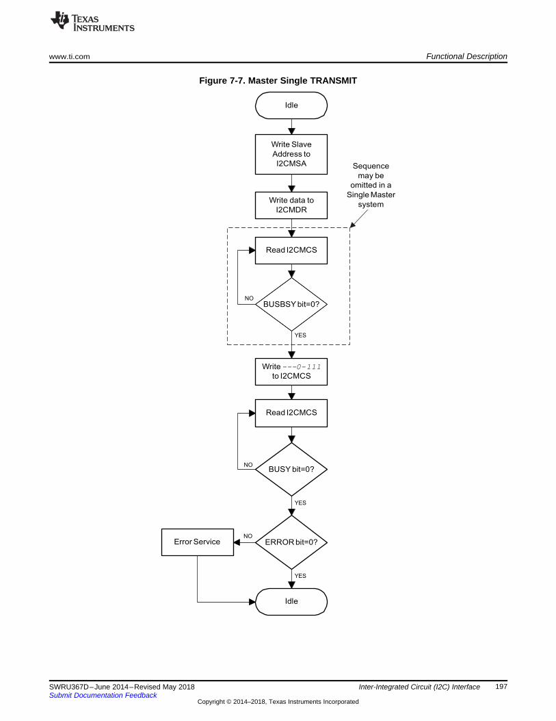
Idle
Write Slave
Address to
I2CMSA
Write data to
I2CMDR
Sequence
may be
omitted in a
Single Master
system
Read I2CMCS
NOBUSBSY bit=0?
YES
Write---0-111
to I2CMCS
Read I2CMCS
NOBUSY bit=0?
YES
Error ServiceNO
ERROR bit=0?
YES
Idle
www.ti.com Functional Description
197SWRU367D–June 2014–Revised May 2018Submit Documentation Feedback
Copyright © 2014–2018, Texas Instruments Incorporated
Inter-Integrated Circuit (I2C) Interface
Figure 7-7. Master Single TRANSMIT
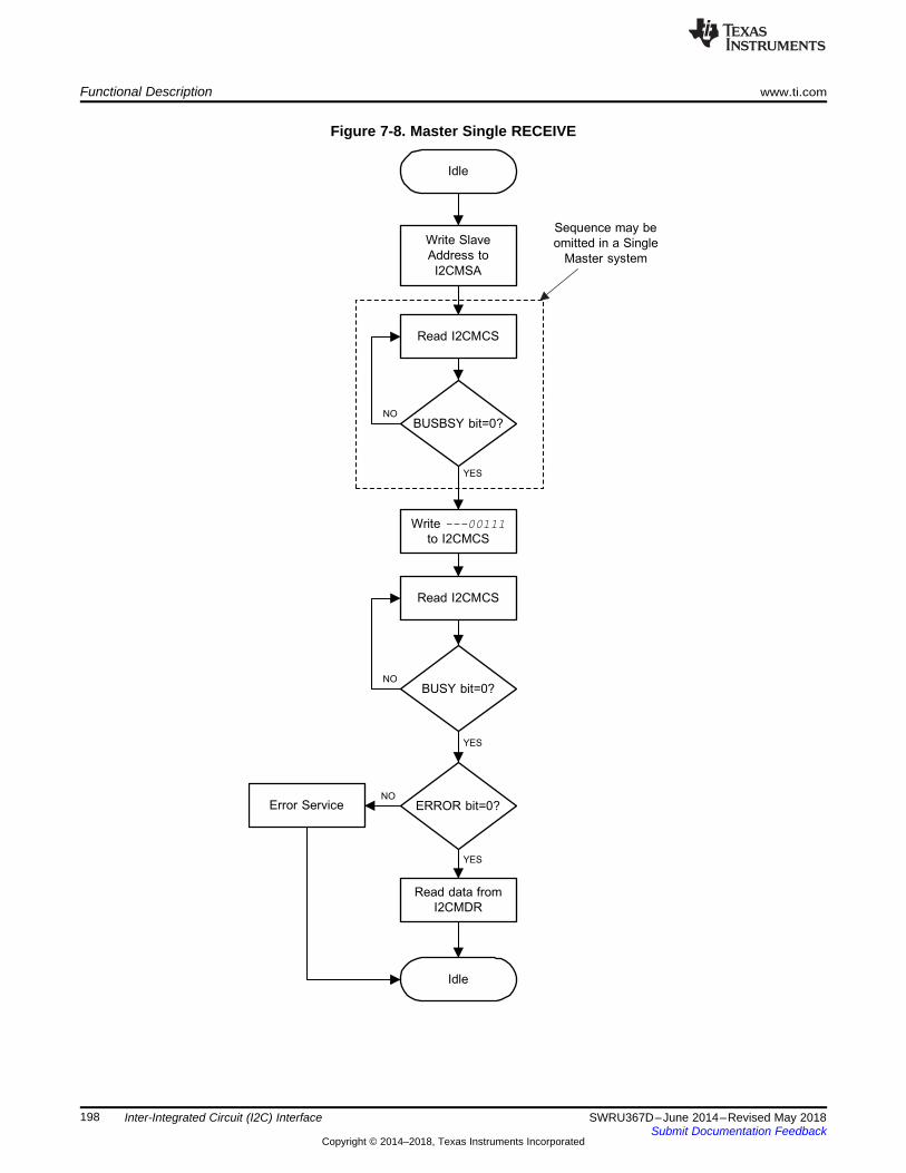
Master
Idle
Write Slave
Address to
I2CMSA
Sequence may be
omitted in a Single
system
Read I2CMCS
NOBUSBSY bit=0?
YES
Write ---00111
to I2CMCS
Read I2CMCS
NOBUSY bit=0?
YES
Error ServiceNO
ERROR bit=0?
YES
Read data from
I2CMDR
Idle
Functional Description www.ti.com
198 SWRU367D–June 2014–Revised May 2018Submit Documentation Feedback
Copyright © 2014–2018, Texas Instruments Incorporated
Inter-Integrated Circuit (I2C) Interface
Figure 7-8. Master Single RECEIVE

Idle
Write Slave
Address to
I2CMSA
Write data to
I2CMDR
Sequence
may be
omitted in a
Single Master
system
Read I2CMCS
NOBUSY bit=0?
Read I2CMCSYES
NOERROR bit=0?
NOBUSBSY bit=0?
YES
YESWrite data to
I2CMDR
NOARBLST bit=1?
Write ---0-011
to I2CMCS
Write ---0-001 NO
to I2CMCSIndex=n?
Write ---0-100
to I2CMCS
YES
YESError Service
Write ---0-101
to I2CMCSIdle
Read I2CMCS
NOBUSY bit=0?
YES
Error ServiceNO
ERROR bit=0?
YES
Idle
www.ti.com Functional Description
199SWRU367D–June 2014–Revised May 2018Submit Documentation Feedback
Copyright © 2014–2018, Texas Instruments Incorporated
Inter-Integrated Circuit (I2C) Interface
Figure 7-9. Master TRANSMIT of Multiple Data Bytes
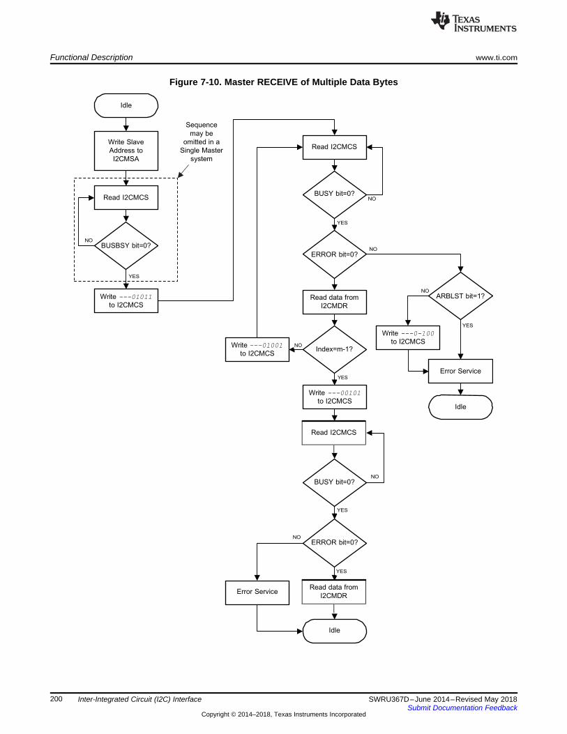
Read data from
I2CMDR
Idle
Write Slave
Address to
I2CMSA
Sequence
may be
omitted in a
Single Master
system
Read I2CMCS
Read I2CMCSBUSY bit=0?
NO
YES
NOBUSBSY bit=0?
NOERROR bit=0?
YES
Write ---01011
to I2CMCSRead data from
I2CMDR
NOARBLST bit=1?
Write ---01001 NO
to I2CMCSIndex=m-1?
Write ---0-100
to I2CMCS
YES
YESError Service
Write ---00101
to I2CMCSIdle
Read I2CMCS
NOBUSY bit=0?
YES
NOERROR bit=0?
Error Service
YES
Idle
Functional Description www.ti.com
200 SWRU367D–June 2014–Revised May 2018Submit Documentation Feedback
Copyright © 2014–2018, Texas Instruments Incorporated
Inter-Integrated Circuit (I2C) Interface
Figure 7-10. Master RECEIVE of Multiple Data Bytes
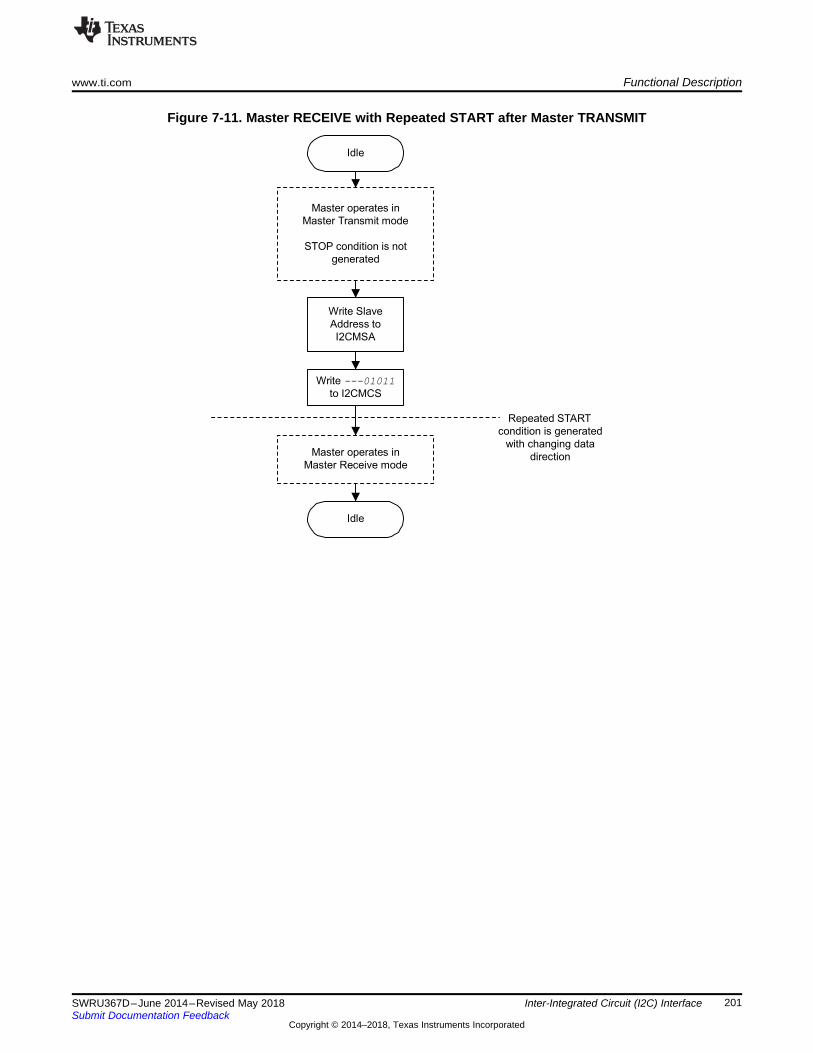
Idle
Master operates in
Master Transmit mode
STOP condition is not
generated
Write Slave
Address to
I2CMSA
Write ---01011
to I2CMCS
Master operates in
Master Receive mode
Repeated START
condition is generated
with changing data
direction
Idle
www.ti.com Functional Description
201SWRU367D–June 2014–Revised May 2018Submit Documentation Feedback
Copyright © 2014–2018, Texas Instruments Incorporated
Inter-Integrated Circuit (I2C) Interface
Figure 7-11. Master RECEIVE with Repeated START after Master TRANSMIT
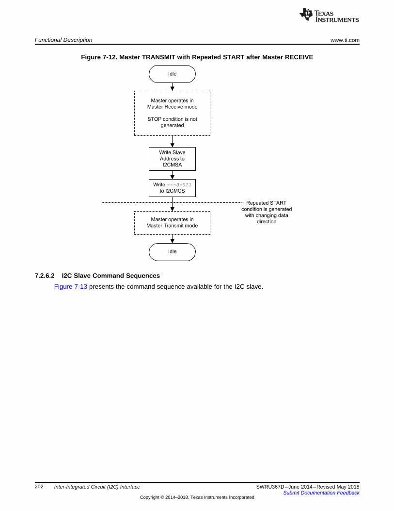
Idle
Master operates in
Master Receive mode
STOP condition is not
generated
Write Slave
Address to
I2CMSA
Write ---0-011
to I2CMCS
Master operates in
Master Transmit mode
Repeated START
condition is generated
with changing data
direction
Idle
Functional Description www.ti.com
202 SWRU367D–June 2014–Revised May 2018Submit Documentation Feedback
Copyright © 2014–2018, Texas Instruments Incorporated
Inter-Integrated Circuit (I2C) Interface
Figure 7-12. Master TRANSMIT with Repeated START after Master RECEIVE
7.2.6.2 I2C Slave Command SequencesFigure 7-13 presents the command sequence available for the I2C slave.
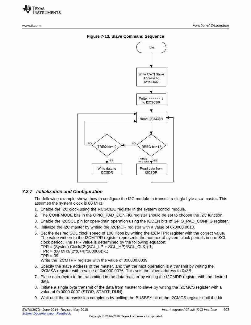
Idle
Write OWN Slave
Address to
I2CSOAR
Write ------ 1
to I2CSCSR
Read I2CSCSR
NO
TREQ bit=1?
NO
RREQ bit=1?
YESFBR is
also validYES
Write data to
I2CSDR
Read data from
I2CSDR
www.ti.com Functional Description
203SWRU367D–June 2014–Revised May 2018Submit Documentation Feedback
Copyright © 2014–2018, Texas Instruments Incorporated
Inter-Integrated Circuit (I2C) Interface
Figure 7-13. Slave Command Sequence
7.2.7 Initialization and ConfigurationThe following example shows how to configure the I2C module to transmit a single byte as a master. Thisassumes the system clock is 80 MHz.1. Enable the I2C clock using the RCGCI2C register in the system control module.2. The CONFMODE bits in the GPIO_PAD_CONFIG register should be set to choose the I2C function.3. Enable the I2CSCL pin for open-drain operation using the IODEN bits of GPIO_PAD_CONFIG register.4. Initialize the I2C master by writing the I2CMCR register with a value of 0x0000.0010.5. Set the desired SCL clock speed of 100 Kbps by writing the I2CMTPR register with the correct value.
The value written to the I2CMTPR register represents the number of system clock periods in one SCLclock period. The TPR value is determined by the following equation:TPR = (System Clock/(2*(SCL_LP + SCL_HP)*SCL_CLK))-1;TPR = (80 MHz/(2*(6+4)*100000))-1;TPR = 39Write the I2CMTPR register with the value of 0x0000.0039.
6. Specify the slave address of the master, and that the next operation is a transmit by writing theI2CMSA register with a value of 0x0000.0076. This sets the slave address to 0x3B.
7. Place data (byte) to be transmitted in the data register by writing the I2CMDR register with the desireddata.
8. Initiate a single byte transmit of the data from master to slave by writing the I2CMCS register with avalue of 0x0000.0007 (STOP, START, RUN).
9. Wait until the transmission completes by polling the BUSBSY bit of the I2CMCS register until the bit
Register Map www.ti.com
204 SWRU367D–June 2014–Revised May 2018Submit Documentation Feedback
Copyright © 2014–2018, Texas Instruments Incorporated
Inter-Integrated Circuit (I2C) Interface
has been cleared.10. Check the ERROR bit in the I2CMCS register to confirm the transmit was acknowledged.
7.3 Register Map
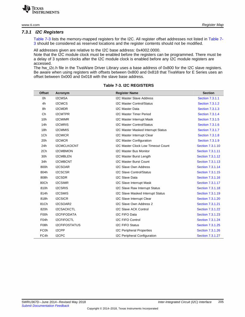
www.ti.com Register Map
205SWRU367D–June 2014–Revised May 2018Submit Documentation Feedback
Copyright © 2014–2018, Texas Instruments Incorporated
Inter-Integrated Circuit (I2C) Interface
7.3.1 I2C RegistersTable 7-3 lists the memory-mapped registers for the I2C. All register offset addresses not listed in Table 7-3 should be considered as reserved locations and the register contents should not be modified.
All addresses given are relative to the I2C base address: 0x4002.0000.Note that the I2C module clock must be enabled before the registers can be programmed. There must bea delay of 3 system clocks after the I2C module clock is enabled before any I2C module registers areaccessed.The hw_i2c.h file in the TivaWare Driver Library uses a base address of 0x800 for the I2C slave registers.Be aware when using registers with offsets between 0x800 and 0x818 that TivaWare for E Series uses anoffset between 0x000 and 0x018 with the slave base address.
Table 7-3. I2C REGISTERS
Offset Acronym Register Name Section0h I2CMSA I2C Master Slave Address Section 7.3.1.14h I2CMCS I2C Master Control/Status Section 7.3.1.28h I2CMDR I2C Master Data Section 7.3.1.3Ch I2CMTPR I2C Master Timer Period Section 7.3.1.410h I2CMIMR I2C Master Interrupt Mask Section 7.3.1.514h I2CMRIS I2C Master Control/Status Section 7.3.1.618h I2CMMIS I2C Master Masked Interrupt Status Section 7.3.1.71Ch I2CMICR I2C Master Interrupt Clear Section 7.3.1.820h I2CMCR I2C Master Configuration Section 7.3.1.924h I2CMCLKOCNT I2C Master Clock Low Timeout Count Section 7.3.1.102Ch I2CMBMON I2C Master Bus Monitor Section 7.3.1.1130h I2CMBLEN I2C Master Burst Length Section 7.3.1.1234h I2CMBCNT I2C Master Burst Count Section 7.3.1.13800h I2CSOAR I2C Slave Own Address Section 7.3.1.14804h I2CSCSR I2C Slave Control/Status Section 7.3.1.15808h I2CSDR I2C Slave Data Section 7.3.1.1680Ch I2CSIMR I2C Slave Interrupt Mask Section 7.3.1.17810h I2CSRIS I2C Slave Raw Interrupt Status Section 7.3.1.18814h I2CSMIS I2C Slave Masked Interrupt Status Section 7.3.1.19818h I2CSICR I2C Slave Interrupt Clear Section 7.3.1.2081Ch I2CSOAR2 I2C Slave Own Address 2 Section 7.3.1.21820h I2CSACKCTL I2C Slave ACK Control Section 7.3.1.22F00h I2CFIFODATA I2C FIFO Data Section 7.3.1.23F04h I2CFIFOCTL I2C FIFO Control Section 7.3.1.24F08h I2CFIFOSTATUS I2C FIFO Status Section 7.3.1.25FC0h I2CPP I2C Peripheral Properties Section 7.3.1.26FC4h I2CPC I2C Peripheral Configuration Section 7.3.1.27
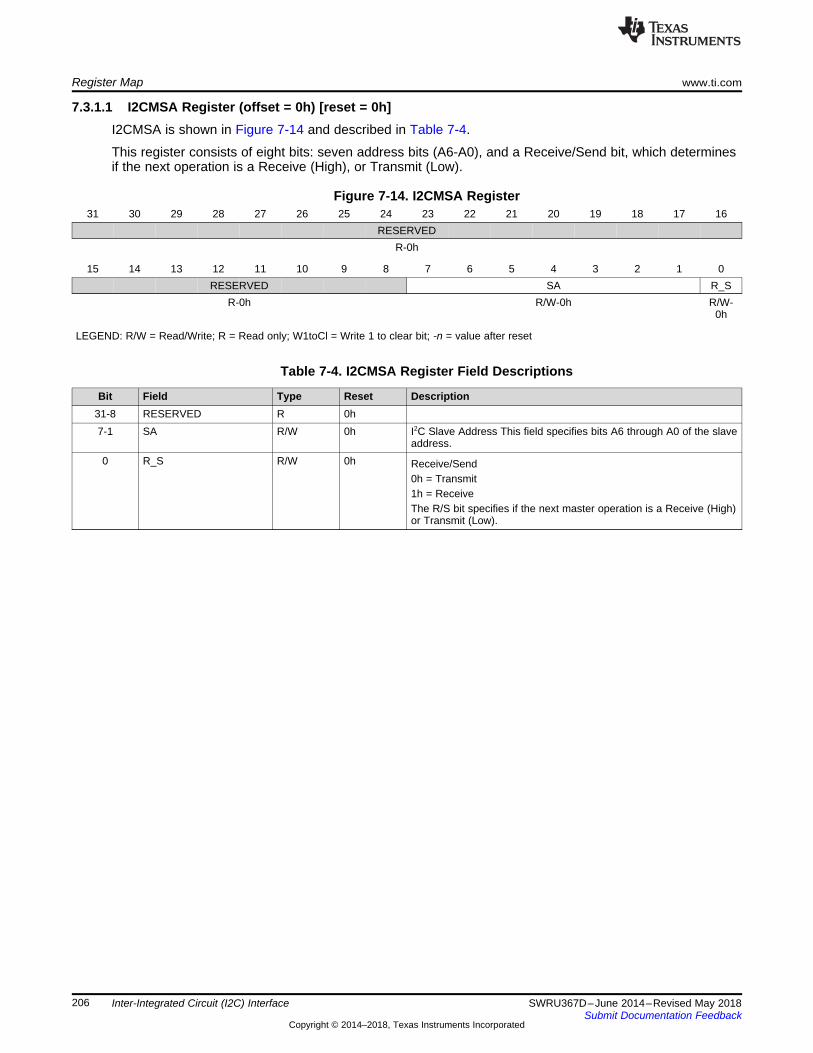
Register Map www.ti.com
206 SWRU367D–June 2014–Revised May 2018Submit Documentation Feedback
Copyright © 2014–2018, Texas Instruments Incorporated
Inter-Integrated Circuit (I2C) Interface
7.3.1.1 I2CMSA Register (offset = 0h) [reset = 0h]I2CMSA is shown in Figure 7-14 and described in Table 7-4.
This register consists of eight bits: seven address bits (A6-A0), and a Receive/Send bit, which determinesif the next operation is a Receive (High), or Transmit (Low).
Figure 7-14. I2CMSA Register31 30 29 28 27 26 25 24 23 22 21 20 19 18 17 16
RESERVEDR-0h
15 14 13 12 11 10 9 8 7 6 5 4 3 2 1 0RESERVED SA R_S
R-0h R/W-0h R/W-0h
LEGEND: R/W = Read/Write; R = Read only; W1toCl = Write 1 to clear bit; -n = value after reset
Table 7-4. I2CMSA Register Field Descriptions
Bit Field Type Reset Description31-8 RESERVED R 0h7-1 SA R/W 0h I2C Slave Address This field specifies bits A6 through A0 of the slave
address.0 R_S R/W 0h Receive/Send
0h = Transmit1h = ReceiveThe R/S bit specifies if the next master operation is a Receive (High)or Transmit (Low).
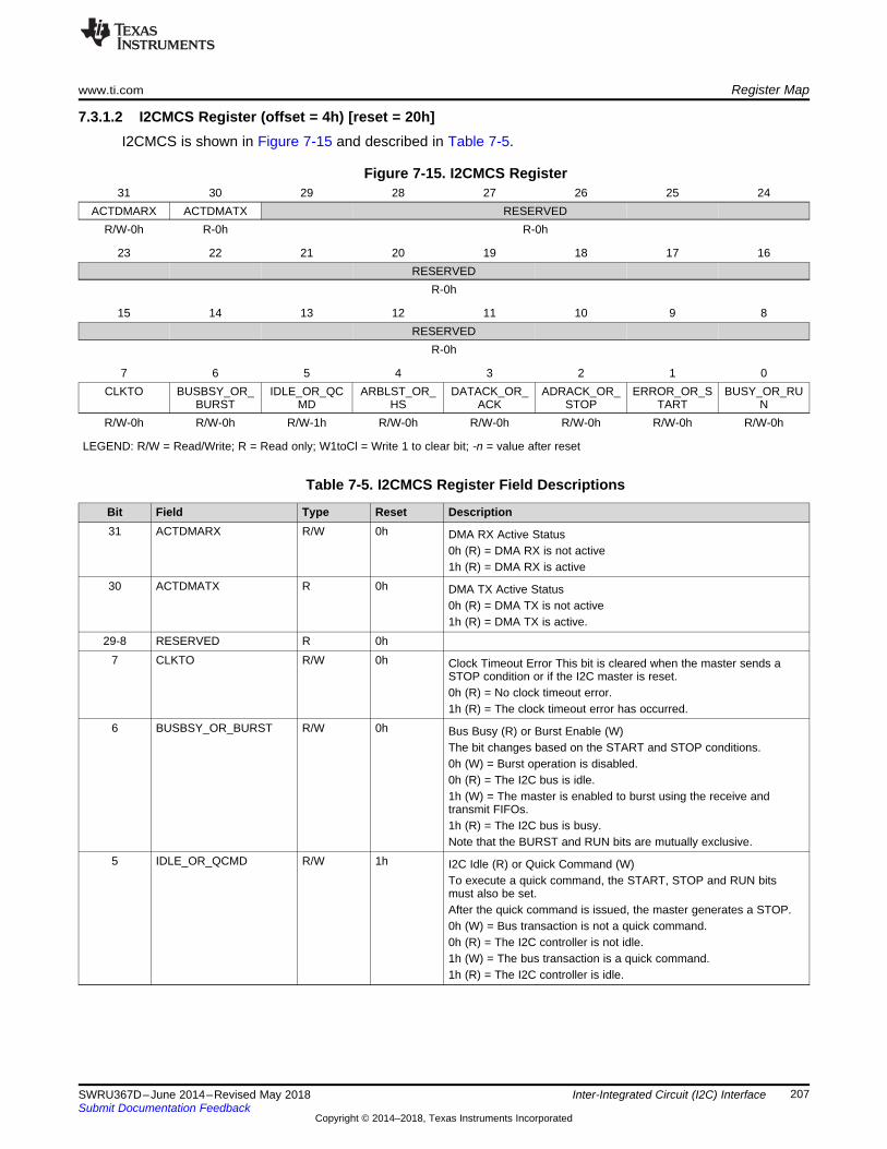
www.ti.com Register Map
207SWRU367D–June 2014–Revised May 2018Submit Documentation Feedback
Copyright © 2014–2018, Texas Instruments Incorporated
Inter-Integrated Circuit (I2C) Interface
7.3.1.2 I2CMCS Register (offset = 4h) [reset = 20h]I2CMCS is shown in Figure 7-15 and described in Table 7-5.
Figure 7-15. I2CMCS Register31 30 29 28 27 26 25 24
ACTDMARX ACTDMATX RESERVEDR/W-0h R-0h R-0h
23 22 21 20 19 18 17 16RESERVED
R-0h
15 14 13 12 11 10 9 8RESERVED
R-0h
7 6 5 4 3 2 1 0CLKTO BUSBSY_OR_
BURSTIDLE_OR_QC
MDARBLST_OR_
HSDATACK_OR_
ACKADRACK_OR_
STOPERROR_OR_S
TARTBUSY_OR_RU
NR/W-0h R/W-0h R/W-1h R/W-0h R/W-0h R/W-0h R/W-0h R/W-0h
LEGEND: R/W = Read/Write; R = Read only; W1toCl = Write 1 to clear bit; -n = value after reset
Table 7-5. I2CMCS Register Field Descriptions
Bit Field Type Reset Description31 ACTDMARX R/W 0h DMA RX Active Status
0h (R) = DMA RX is not active1h (R) = DMA RX is active
30 ACTDMATX R 0h DMA TX Active Status0h (R) = DMA TX is not active1h (R) = DMA TX is active.
29-8 RESERVED R 0h7 CLKTO R/W 0h Clock Timeout Error This bit is cleared when the master sends a
STOP condition or if the I2C master is reset.0h (R) = No clock timeout error.1h (R) = The clock timeout error has occurred.
6 BUSBSY_OR_BURST R/W 0h Bus Busy (R) or Burst Enable (W)The bit changes based on the START and STOP conditions.0h (W) = Burst operation is disabled.0h (R) = The I2C bus is idle.1h (W) = The master is enabled to burst using the receive andtransmit FIFOs.1h (R) = The I2C bus is busy.Note that the BURST and RUN bits are mutually exclusive.
5 IDLE_OR_QCMD R/W 1h I2C Idle (R) or Quick Command (W)To execute a quick command, the START, STOP and RUN bitsmust also be set.After the quick command is issued, the master generates a STOP.0h (W) = Bus transaction is not a quick command.0h (R) = The I2C controller is not idle.1h (W) = The bus transaction is a quick command.1h (R) = The I2C controller is idle.
Register Map www.ti.com
208 SWRU367D–June 2014–Revised May 2018Submit Documentation Feedback
Copyright © 2014–2018, Texas Instruments Incorporated
Inter-Integrated Circuit (I2C) Interface
Table 7-5. I2CMCS Register Field Descriptions (continued)Bit Field Type Reset Description4 ARBLST_OR_HS R/W 0h Arbitration Lost (R) or Reserved (High-Speed Enable Not Supported)
(W)0h (W) = The master operates in Standard or Fast mode as selectedby using a value in the I2CMTPR register that results in an SCLfrequency of 100 kbps for Standard mode or 400 kbps for Fastmode.0h (R) = The I2C controller won arbitration.1h (R) = The I2C controller lost arbitration.
3 DATACK_OR_ACK R/W 0h Acknowledge Data (R) or Data Acknowledge Enable (W)0h (W) = The received data byte is not acknowledged automaticallyby the master.0h (R) = The transmitted data was acknowledged1h (W) = The received data byte is acknowledged automatically bythe master.1h (R) = The transmitted data was not acknowledged.
2 ADRACK_OR_STOP R/W 0h Acknowledge Address (R) or Generate STOP (W)0h (W) = The controller does not generate the STOP condition.0h (R) = The transmitted address was acknowledged1h (W) = The controller generates the STOP condition.1h (R) = The transmitted address was not acknowledged.
1 ERROR_OR_START R/W 0h Error (R) or Generate START (W)The error can be when the slave address is not acknowledged, orwhen the transmit data is not acknowledged.0h (W) = The controller does not generate the START condition.0h (R) = No error was detected on the last operation.1h (W) = The controller generates the START or repeated STARTcondition.1h (R) = An error occurred on the last operation.
0 BUSY_OR_RUN R/W 0h I2C Busy (R) or I2C Master Enable (W)When the BUSY bit is set, the other status bits are not valid.Note that the BURST and RUN bits are mutually exclusive.0h (W) = In standard mode, this encoding means the master isunable to transmit or receive data. In Burst mode, this bit is not usedand must be set to 0.0h (R) = The controller is idle.1h (W) = The master is able to transmit or receive data. Note thatthis bit cannot be set in Burst mode.1h (R) = The controller is busy.
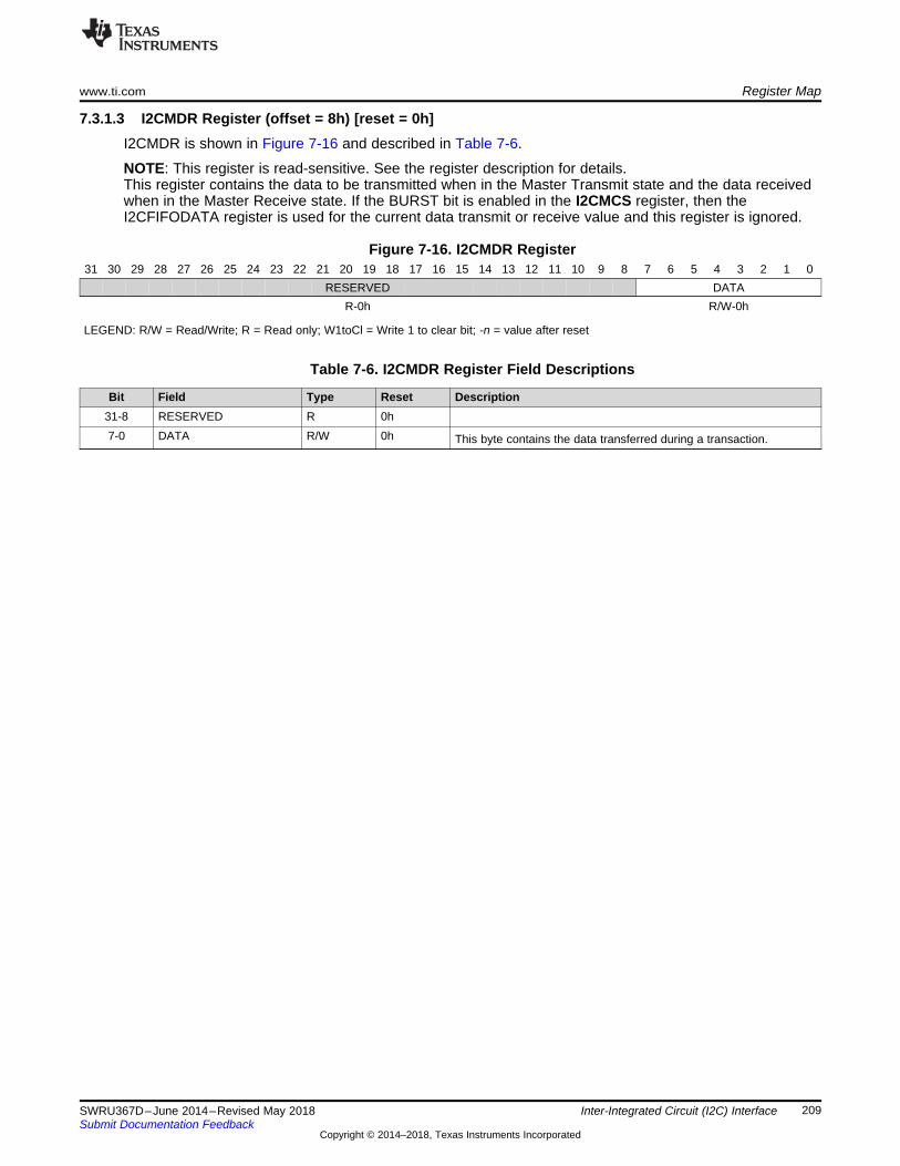
www.ti.com Register Map
209SWRU367D–June 2014–Revised May 2018Submit Documentation Feedback
Copyright © 2014–2018, Texas Instruments Incorporated
Inter-Integrated Circuit (I2C) Interface
7.3.1.3 I2CMDR Register (offset = 8h) [reset = 0h]I2CMDR is shown in Figure 7-16 and described in Table 7-6.
NOTE: This register is read-sensitive. See the register description for details.This register contains the data to be transmitted when in the Master Transmit state and the data receivedwhen in the Master Receive state. If the BURST bit is enabled in the I2CMCS register, then theI2CFIFODATA register is used for the current data transmit or receive value and this register is ignored.
Figure 7-16. I2CMDR Register31 30 29 28 27 26 25 24 23 22 21 20 19 18 17 16 15 14 13 12 11 10 9 8 7 6 5 4 3 2 1 0
RESERVED DATAR-0h R/W-0h
LEGEND: R/W = Read/Write; R = Read only; W1toCl = Write 1 to clear bit; -n = value after reset
Table 7-6. I2CMDR Register Field Descriptions
Bit Field Type Reset Description31-8 RESERVED R 0h7-0 DATA R/W 0h This byte contains the data transferred during a transaction.
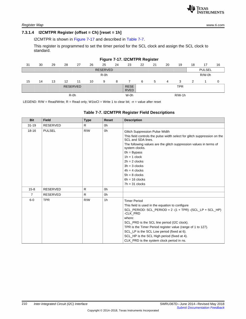
Register Map www.ti.com
210 SWRU367D–June 2014–Revised May 2018Submit Documentation Feedback
Copyright © 2014–2018, Texas Instruments Incorporated
Inter-Integrated Circuit (I2C) Interface
7.3.1.4 I2CMTPR Register (offset = Ch) [reset = 1h]I2CMTPR is shown in Figure 7-17 and described in Table 7-7.
This register is programmed to set the timer period for the SCL clock and assign the SCL clock tostandard.
Figure 7-17. I2CMTPR Register31 30 29 28 27 26 25 24 23 22 21 20 19 18 17 16
RESERVED PULSELR-0h R/W-0h
15 14 13 12 11 10 9 8 7 6 5 4 3 2 1 0RESERVED RESE
RVEDTPR
R-0h W-0h R/W-1h
LEGEND: R/W = Read/Write; R = Read only; W1toCl = Write 1 to clear bit; -n = value after reset
Table 7-7. I2CMTPR Register Field Descriptions
Bit Field Type Reset Description31-19 RESERVED R 0h18-16 PULSEL R/W 0h Glitch Suppression Pulse Width
This field controls the pulse width select for glitch suppression on theSCL and SDA lines.The following values are the glitch suppression values in terms ofsystem clocks.0h = Bypass1h = 1 clock2h = 2 clocks3h = 3 clocks4h = 4 clocks5h = 8 clocks6h = 16 clocks7h = 31 clocks
15-8 RESERVED R 0h7 RESERVED R 0h
6-0 TPR R/W 1h Timer PeriodThis field is used in the equation to configureSCL_PERIOD: SCL_PERIOD = 2 -(1 + TPR) -(SCL_LP + SCL_HP)-CLK_PRDwhere:SCL_PRD is the SCL line period (I2C clock).TPR is the Timer Period register value (range of 1 to 127).SCL_LP is the SCL Low period (fixed at 6).SCL_HP is the SCL High period (fixed at 4).CLK_PRD is the system clock period in ns.
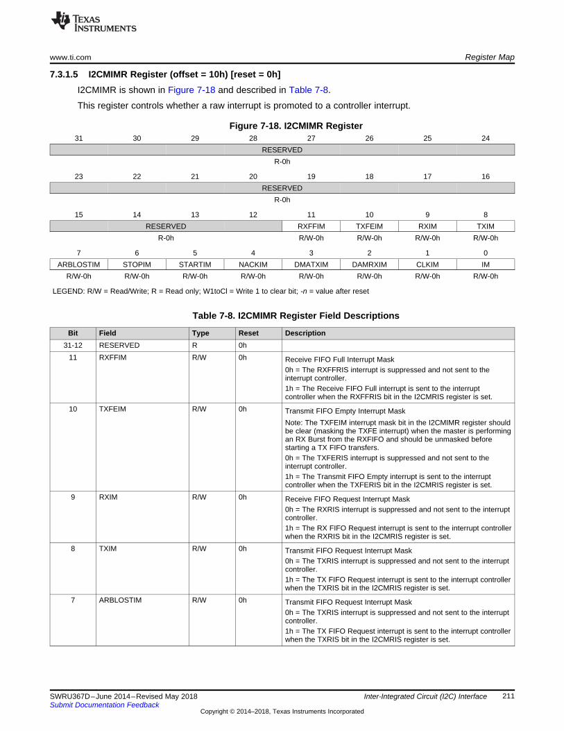
www.ti.com Register Map
211SWRU367D–June 2014–Revised May 2018Submit Documentation Feedback
Copyright © 2014–2018, Texas Instruments Incorporated
Inter-Integrated Circuit (I2C) Interface
7.3.1.5 I2CMIMR Register (offset = 10h) [reset = 0h]I2CMIMR is shown in Figure 7-18 and described in Table 7-8.
This register controls whether a raw interrupt is promoted to a controller interrupt.
Figure 7-18. I2CMIMR Register31 30 29 28 27 26 25 24
RESERVEDR-0h
23 22 21 20 19 18 17 16RESERVED
R-0h
15 14 13 12 11 10 9 8RESERVED RXFFIM TXFEIM RXIM TXIM
R-0h R/W-0h R/W-0h R/W-0h R/W-0h
7 6 5 4 3 2 1 0ARBLOSTIM STOPIM STARTIM NACKIM DMATXIM DAMRXIM CLKIM IM
R/W-0h R/W-0h R/W-0h R/W-0h R/W-0h R/W-0h R/W-0h R/W-0h
LEGEND: R/W = Read/Write; R = Read only; W1toCl = Write 1 to clear bit; -n = value after reset
Table 7-8. I2CMIMR Register Field Descriptions
Bit Field Type Reset Description31-12 RESERVED R 0h
11 RXFFIM R/W 0h Receive FIFO Full Interrupt Mask0h = The RXFFRIS interrupt is suppressed and not sent to theinterrupt controller.1h = The Receive FIFO Full interrupt is sent to the interruptcontroller when the RXFFRIS bit in the I2CMRIS register is set.
10 TXFEIM R/W 0h Transmit FIFO Empty Interrupt MaskNote: The TXFEIM interrupt mask bit in the I2CMIMR register shouldbe clear (masking the TXFE interrupt) when the master is performingan RX Burst from the RXFIFO and should be unmasked beforestarting a TX FIFO transfers.0h = The TXFERIS interrupt is suppressed and not sent to theinterrupt controller.1h = The Transmit FIFO Empty interrupt is sent to the interruptcontroller when the TXFERIS bit in the I2CMRIS register is set.
9 RXIM R/W 0h Receive FIFO Request Interrupt Mask0h = The RXRIS interrupt is suppressed and not sent to the interruptcontroller.1h = The RX FIFO Request interrupt is sent to the interrupt controllerwhen the RXRIS bit in the I2CMRIS register is set.
8 TXIM R/W 0h Transmit FIFO Request Interrupt Mask0h = The TXRIS interrupt is suppressed and not sent to the interruptcontroller.1h = The TX FIFO Request interrupt is sent to the interrupt controllerwhen the TXRIS bit in the I2CMRIS register is set.
7 ARBLOSTIM R/W 0h Transmit FIFO Request Interrupt Mask0h = The TXRIS interrupt is suppressed and not sent to the interruptcontroller.1h = The TX FIFO Request interrupt is sent to the interrupt controllerwhen the TXRIS bit in the I2CMRIS register is set.
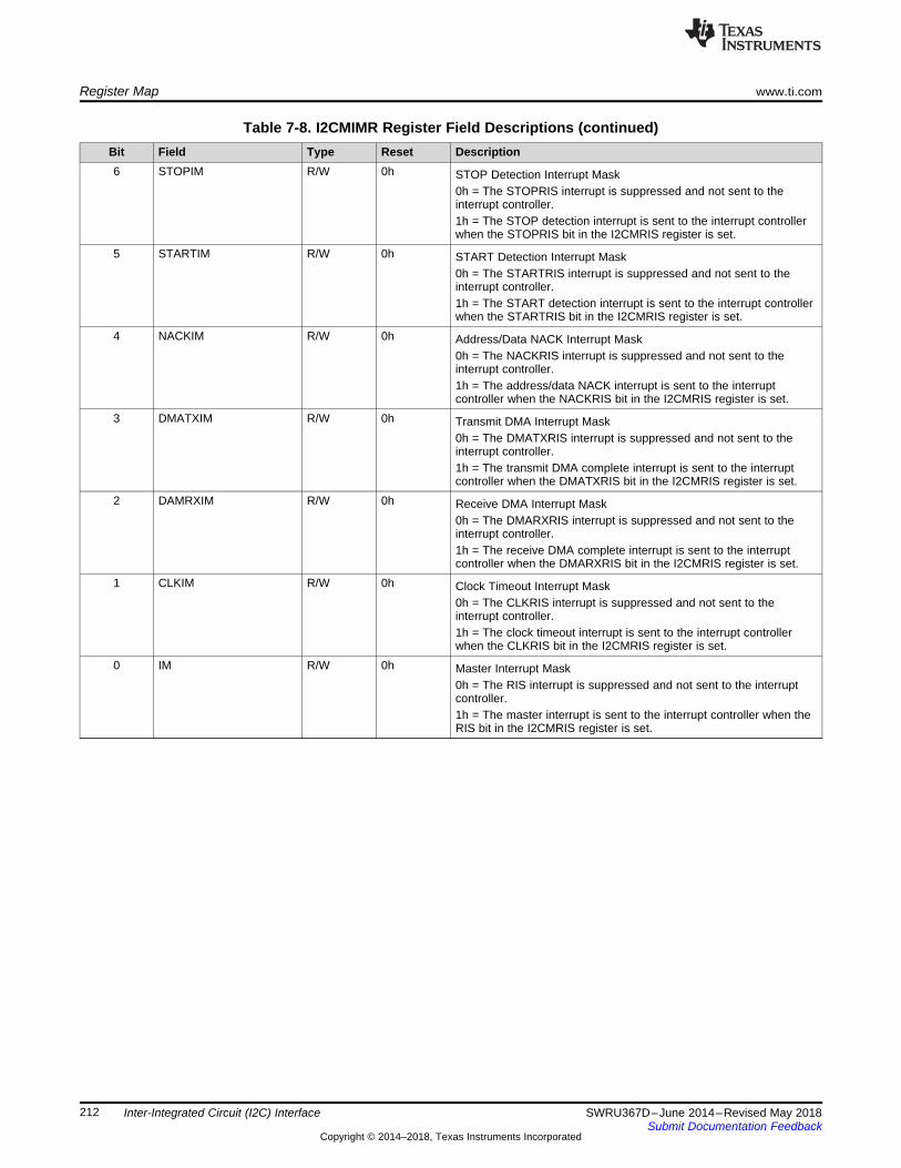
Register Map www.ti.com
212 SWRU367D–June 2014–Revised May 2018Submit Documentation Feedback
Copyright © 2014–2018, Texas Instruments Incorporated
Inter-Integrated Circuit (I2C) Interface
Table 7-8. I2CMIMR Register Field Descriptions (continued)Bit Field Type Reset Description6 STOPIM R/W 0h STOP Detection Interrupt Mask
0h = The STOPRIS interrupt is suppressed and not sent to theinterrupt controller.1h = The STOP detection interrupt is sent to the interrupt controllerwhen the STOPRIS bit in the I2CMRIS register is set.
5 STARTIM R/W 0h START Detection Interrupt Mask0h = The STARTRIS interrupt is suppressed and not sent to theinterrupt controller.1h = The START detection interrupt is sent to the interrupt controllerwhen the STARTRIS bit in the I2CMRIS register is set.
4 NACKIM R/W 0h Address/Data NACK Interrupt Mask0h = The NACKRIS interrupt is suppressed and not sent to theinterrupt controller.1h = The address/data NACK interrupt is sent to the interruptcontroller when the NACKRIS bit in the I2CMRIS register is set.
3 DMATXIM R/W 0h Transmit DMA Interrupt Mask0h = The DMATXRIS interrupt is suppressed and not sent to theinterrupt controller.1h = The transmit DMA complete interrupt is sent to the interruptcontroller when the DMATXRIS bit in the I2CMRIS register is set.
2 DAMRXIM R/W 0h Receive DMA Interrupt Mask0h = The DMARXRIS interrupt is suppressed and not sent to theinterrupt controller.1h = The receive DMA complete interrupt is sent to the interruptcontroller when the DMARXRIS bit in the I2CMRIS register is set.
1 CLKIM R/W 0h Clock Timeout Interrupt Mask0h = The CLKRIS interrupt is suppressed and not sent to theinterrupt controller.1h = The clock timeout interrupt is sent to the interrupt controllerwhen the CLKRIS bit in the I2CMRIS register is set.
0 IM R/W 0h Master Interrupt Mask0h = The RIS interrupt is suppressed and not sent to the interruptcontroller.1h = The master interrupt is sent to the interrupt controller when theRIS bit in the I2CMRIS register is set.
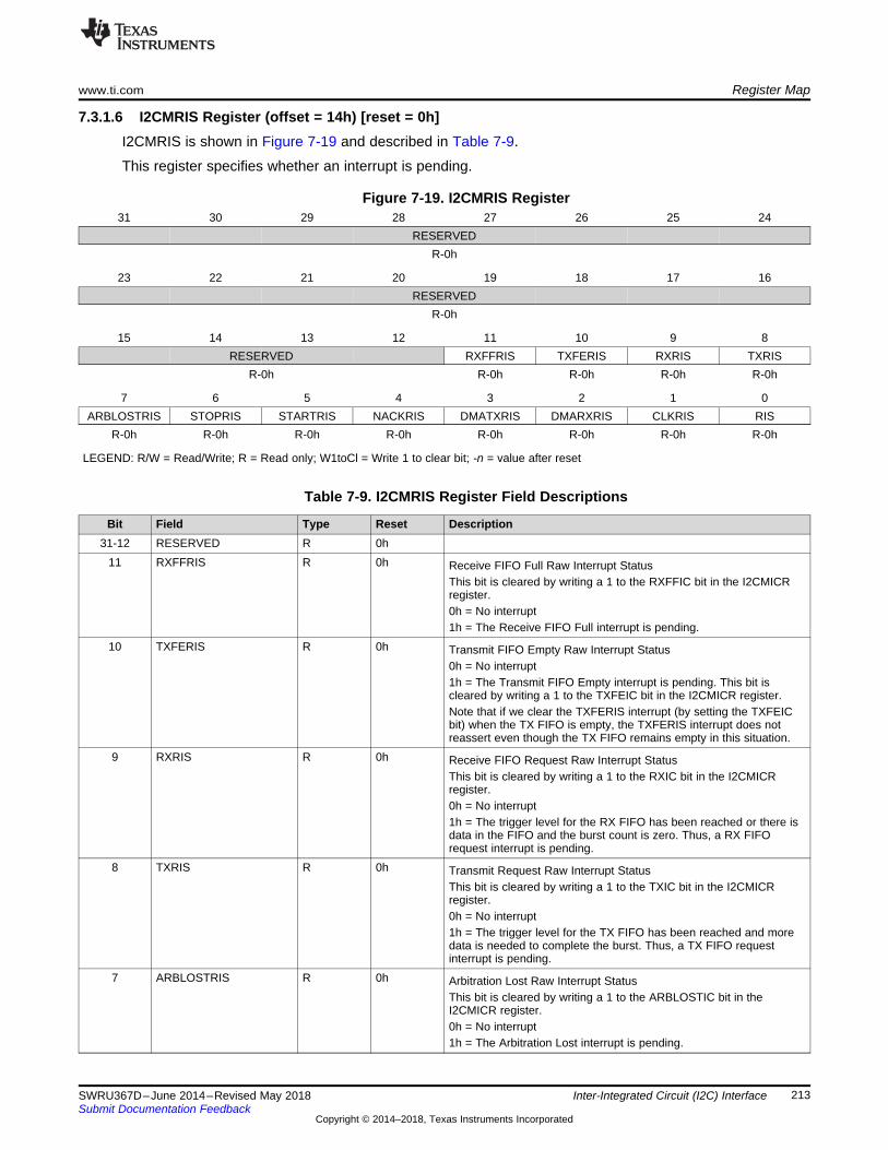
www.ti.com Register Map
213SWRU367D–June 2014–Revised May 2018Submit Documentation Feedback
Copyright © 2014–2018, Texas Instruments Incorporated
Inter-Integrated Circuit (I2C) Interface
7.3.1.6 I2CMRIS Register (offset = 14h) [reset = 0h]I2CMRIS is shown in Figure 7-19 and described in Table 7-9.
This register specifies whether an interrupt is pending.
Figure 7-19. I2CMRIS Register31 30 29 28 27 26 25 24
RESERVEDR-0h
23 22 21 20 19 18 17 16RESERVED
R-0h
15 14 13 12 11 10 9 8RESERVED RXFFRIS TXFERIS RXRIS TXRIS
R-0h R-0h R-0h R-0h R-0h
7 6 5 4 3 2 1 0ARBLOSTRIS STOPRIS STARTRIS NACKRIS DMATXRIS DMARXRIS CLKRIS RIS
R-0h R-0h R-0h R-0h R-0h R-0h R-0h R-0h
LEGEND: R/W = Read/Write; R = Read only; W1toCl = Write 1 to clear bit; -n = value after reset
Table 7-9. I2CMRIS Register Field Descriptions
Bit Field Type Reset Description31-12 RESERVED R 0h
11 RXFFRIS R 0h Receive FIFO Full Raw Interrupt StatusThis bit is cleared by writing a 1 to the RXFFIC bit in the I2CMICRregister.0h = No interrupt1h = The Receive FIFO Full interrupt is pending.
10 TXFERIS R 0h Transmit FIFO Empty Raw Interrupt Status0h = No interrupt1h = The Transmit FIFO Empty interrupt is pending. This bit iscleared by writing a 1 to the TXFEIC bit in the I2CMICR register.Note that if we clear the TXFERIS interrupt (by setting the TXFEICbit) when the TX FIFO is empty, the TXFERIS interrupt does notreassert even though the TX FIFO remains empty in this situation.
9 RXRIS R 0h Receive FIFO Request Raw Interrupt StatusThis bit is cleared by writing a 1 to the RXIC bit in the I2CMICRregister.0h = No interrupt1h = The trigger level for the RX FIFO has been reached or there isdata in the FIFO and the burst count is zero. Thus, a RX FIFOrequest interrupt is pending.
8 TXRIS R 0h Transmit Request Raw Interrupt StatusThis bit is cleared by writing a 1 to the TXIC bit in the I2CMICRregister.0h = No interrupt1h = The trigger level for the TX FIFO has been reached and moredata is needed to complete the burst. Thus, a TX FIFO requestinterrupt is pending.
7 ARBLOSTRIS R 0h Arbitration Lost Raw Interrupt StatusThis bit is cleared by writing a 1 to the ARBLOSTIC bit in theI2CMICR register.0h = No interrupt1h = The Arbitration Lost interrupt is pending.
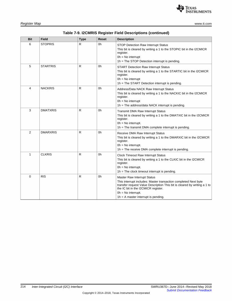
Register Map www.ti.com
214 SWRU367D–June 2014–Revised May 2018Submit Documentation Feedback
Copyright © 2014–2018, Texas Instruments Incorporated
Inter-Integrated Circuit (I2C) Interface
Table 7-9. I2CMRIS Register Field Descriptions (continued)Bit Field Type Reset Description6 STOPRIS R 0h STOP Detection Raw Interrupt Status
This bit is cleared by writing a 1 to the STOPIC bit in the I2CMICRregister.0h = No interrupt1h = The STOP Detection interrupt is pending.
5 STARTRIS R 0h START Detection Raw Interrupt StatusThis bit is cleared by writing a 1 to the STARTIC bit in the I2CMICRregister.0h = No interrupt1h = The START Detection interrupt is pending.
4 NACKRIS R 0h Address/Data NACK Raw Interrupt StatusThis bit is cleared by writing a 1 to the NACKIC bit in the I2CMICRregister.0h = No interrupt1h = The address/data NACK interrupt is pending.
3 DMATXRIS R 0h Transmit DMA Raw Interrupt StatusThis bit is cleared by writing a 1 to the DMATXIC bit in the I2CMICRregister.0h = No interrupt.1h = The transmit DMA complete interrupt is pending.
2 DMARXRIS R 0h Receive DMA Raw Interrupt StatusThis bit is cleared by writing a 1 to the DMARXIC bit in the I2CMICRregister.0h = No interrupt.1h = The receive DMA complete interrupt is pending.
1 CLKRIS R 0h Clock Timeout Raw Interrupt StatusThis bit is cleared by writing a 1 to the CLKIC bit in the I2CMICRregister.0h = No interrupt.1h = The clock timeout interrupt is pending.
0 RIS R 0h Master Raw Interrupt StatusThis interrupt includes: Master transaction completed Next bytetransfer request Value Description This bit is cleared by writing a 1 tothe IC bit in the I2CMICR register.0h = No interrupt.1h = A master interrupt is pending.
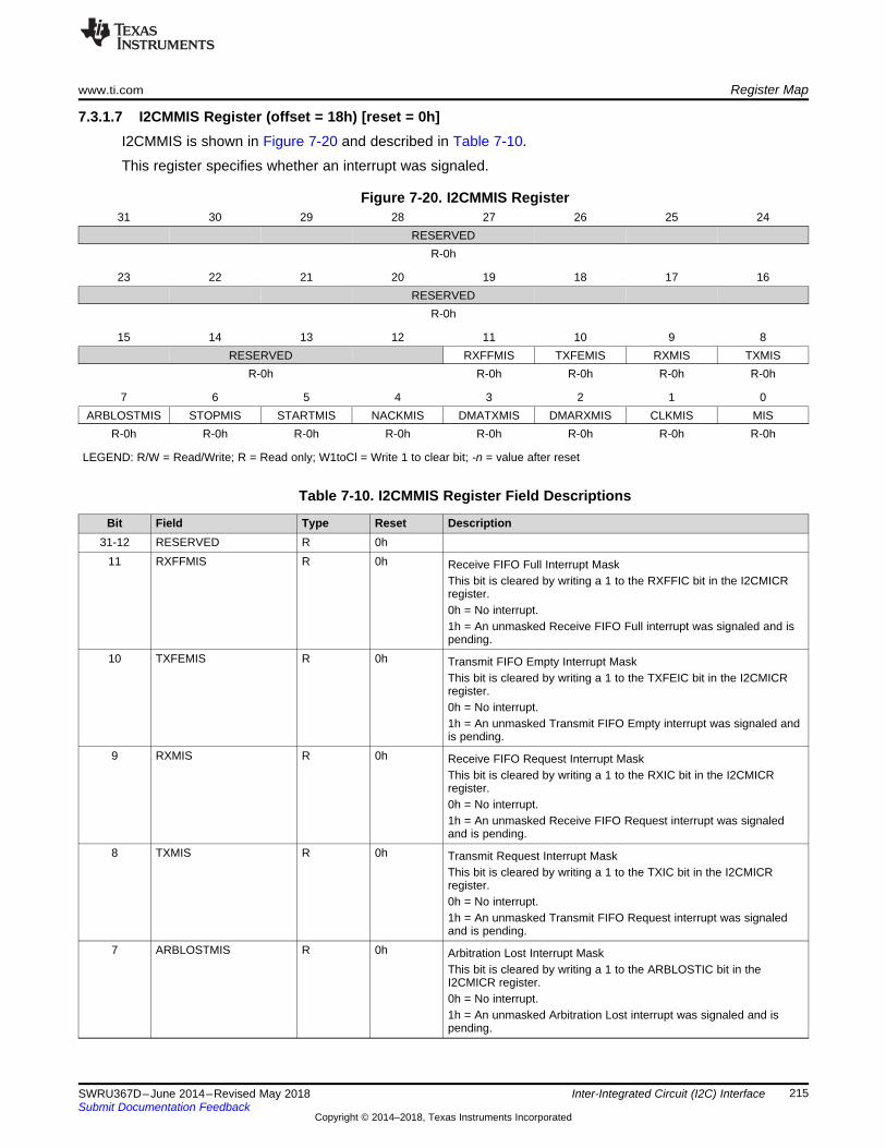
www.ti.com Register Map
215SWRU367D–June 2014–Revised May 2018Submit Documentation Feedback
Copyright © 2014–2018, Texas Instruments Incorporated
Inter-Integrated Circuit (I2C) Interface
7.3.1.7 I2CMMIS Register (offset = 18h) [reset = 0h]I2CMMIS is shown in Figure 7-20 and described in Table 7-10.
This register specifies whether an interrupt was signaled.
Figure 7-20. I2CMMIS Register31 30 29 28 27 26 25 24
RESERVEDR-0h
23 22 21 20 19 18 17 16RESERVED
R-0h
15 14 13 12 11 10 9 8RESERVED RXFFMIS TXFEMIS RXMIS TXMIS
R-0h R-0h R-0h R-0h R-0h
7 6 5 4 3 2 1 0ARBLOSTMIS STOPMIS STARTMIS NACKMIS DMATXMIS DMARXMIS CLKMIS MIS
R-0h R-0h R-0h R-0h R-0h R-0h R-0h R-0h
LEGEND: R/W = Read/Write; R = Read only; W1toCl = Write 1 to clear bit; -n = value after reset
Table 7-10. I2CMMIS Register Field Descriptions
Bit Field Type Reset Description31-12 RESERVED R 0h
11 RXFFMIS R 0h Receive FIFO Full Interrupt MaskThis bit is cleared by writing a 1 to the RXFFIC bit in the I2CMICRregister.0h = No interrupt.1h = An unmasked Receive FIFO Full interrupt was signaled and ispending.
10 TXFEMIS R 0h Transmit FIFO Empty Interrupt MaskThis bit is cleared by writing a 1 to the TXFEIC bit in the I2CMICRregister.0h = No interrupt.1h = An unmasked Transmit FIFO Empty interrupt was signaled andis pending.
9 RXMIS R 0h Receive FIFO Request Interrupt MaskThis bit is cleared by writing a 1 to the RXIC bit in the I2CMICRregister.0h = No interrupt.1h = An unmasked Receive FIFO Request interrupt was signaledand is pending.
8 TXMIS R 0h Transmit Request Interrupt MaskThis bit is cleared by writing a 1 to the TXIC bit in the I2CMICRregister.0h = No interrupt.1h = An unmasked Transmit FIFO Request interrupt was signaledand is pending.
7 ARBLOSTMIS R 0h Arbitration Lost Interrupt MaskThis bit is cleared by writing a 1 to the ARBLOSTIC bit in theI2CMICR register.0h = No interrupt.1h = An unmasked Arbitration Lost interrupt was signaled and ispending.
Register Map www.ti.com
216 SWRU367D–June 2014–Revised May 2018Submit Documentation Feedback
Copyright © 2014–2018, Texas Instruments Incorporated
Inter-Integrated Circuit (I2C) Interface
Table 7-10. I2CMMIS Register Field Descriptions (continued)Bit Field Type Reset Description6 STOPMIS R 0h STOP Detection Interrupt Mask
This bit is cleared by writing a 1 to the STOPIC bit in the I2CMICRregister.0h = No interrupt.1h = An unmasked STOP Detection interrupt was signaled and ispending.
5 STARTMIS R 0h START Detection Interrupt MaskThis bit is cleared by writing a 1 to the STARTIC bit in the I2CMICRregister.0h = No interrupt.1h = An unmasked START Detection interrupt was signaled and ispending.
4 NACKMIS R 0h Address/Data NACK Interrupt MaskThis bit is cleared by writing a 1 to the NACKIC bit in the I2CMICRregister.0h = No interrupt.1h = An unmasked Address/Data NACK interrupt was signaled andis pending.
3 DMATXMIS R 0h Transmit DMA Interrupt StatusThis bit is cleared by writing a 1 to the DMATXIC bit in the I2CMICRregister.0h = No interrupt.1h = An unmasked transmit DMA complete interrupt was signaledand is pending.
2 DMARXMIS R 0h Receive DMA Interrupt StatusThis bit is cleared by writing a 1 to the DMARXIC bit in the I2CMICRregister.0h = No interrupt.1h = An unmasked receive DMA complete interrupt was signaledand is pending.
1 CLKMIS R 0h Clock Timeout Masked Interrupt StatusThis bit is cleared by writing a 1 to the CLKIC bit in the I2CMICRregister.0h = No interrupt.1h = An unmasked clock timeout interrupt was signaled and ispending.
0 MIS R 0h Clock Timeout Masked Interrupt StatusThis bit is cleared by writing a 1 to the CLKIC bit in the I2CMICRregister.0h = No interrupt.1h = An unmasked clock timeout interrupt was signaled and ispending.
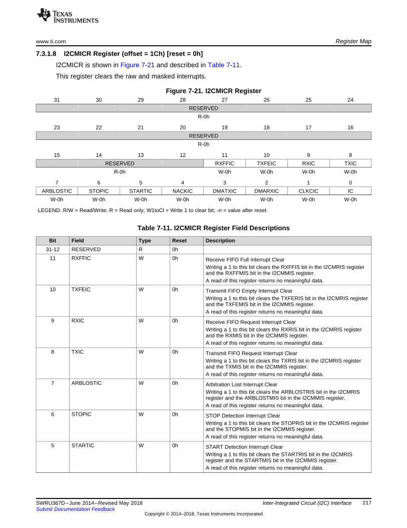
www.ti.com Register Map
217SWRU367D–June 2014–Revised May 2018Submit Documentation Feedback
Copyright © 2014–2018, Texas Instruments Incorporated
Inter-Integrated Circuit (I2C) Interface
7.3.1.8 I2CMICR Register (offset = 1Ch) [reset = 0h]I2CMICR is shown in Figure 7-21 and described in Table 7-11.
This register clears the raw and masked interrupts.
Figure 7-21. I2CMICR Register31 30 29 28 27 26 25 24
RESERVEDR-0h
23 22 21 20 19 18 17 16RESERVED
R-0h
15 14 13 12 11 10 9 8RESERVED RXFFIC TXFEIC RXIC TXIC
R-0h W-0h W-0h W-0h W-0h
7 6 5 4 3 2 1 0ARBLOSTIC STOPIC STARTIC NACKIC DMATXIC DMARXIC CLKCIC IC
W-0h W-0h W-0h W-0h W-0h W-0h W-0h W-0h
LEGEND: R/W = Read/Write; R = Read only; W1toCl = Write 1 to clear bit; -n = value after reset
Table 7-11. I2CMICR Register Field Descriptions
Bit Field Type Reset Description31-12 RESERVED R 0h
11 RXFFIC W 0h Receive FIFO Full Interrupt ClearWriting a 1 to this bit clears the RXFFIS bit in the I2CMRIS registerand the RXFFMIS bit in the I2CMMIS register.A read of this register returns no meaningful data.
10 TXFEIC W 0h Transmit FIFO Empty Interrupt ClearWriting a 1 to this bit clears the TXFERIS bit in the I2CMRIS registerand the TXFEMIS bit in the I2CMMIS register.A read of this register returns no meaningful data.
9 RXIC W 0h Receive FIFO Request Interrupt ClearWriting a 1 to this bit clears the RXRIS bit in the I2CMRIS registerand the RXMIS bit in the I2CMMIS register.A read of this register returns no meaningful data.
8 TXIC W 0h Transmit FIFO Request Interrupt ClearWriting a 1 to this bit clears the TXRIS bit in the I2CMRIS registerand the TXMIS bit in the I2CMMIS register.A read of this register returns no meaningful data.
7 ARBLOSTIC W 0h Arbitration Lost Interrupt ClearWriting a 1 to this bit clears the ARBLOSTRIS bit in the I2CMRISregister and the ARBLOSTMIS bit in the I2CMMIS register.A read of this register returns no meaningful data.
6 STOPIC W 0h STOP Detection Interrupt ClearWriting a 1 to this bit clears the STOPRIS bit in the I2CMRIS registerand the STOPMIS bit in the I2CMMIS register.A read of this register returns no meaningful data.
5 STARTIC W 0h START Detection Interrupt ClearWriting a 1 to this bit clears the STARTRIS bit in the I2CMRISregister and the STARTMIS bit in the I2CMMIS register.A read of this register returns no meaningful data.
Register Map www.ti.com
218 SWRU367D–June 2014–Revised May 2018Submit Documentation Feedback
Copyright © 2014–2018, Texas Instruments Incorporated
Inter-Integrated Circuit (I2C) Interface
Table 7-11. I2CMICR Register Field Descriptions (continued)Bit Field Type Reset Description4 NACKIC W 0h Address/Data NACK Interrupt Clear
Writing a 1 to this bit clears the NACKRIS bit in the I2CMRIS registerand the NACKMIS bit in the I2CMMIS register.A read of this register returns no meaningful data.
3 DMATXIC W 0h Transmit DMA Interrupt ClearWriting a 1 to this bit clears the DMATXRIS bit in the I2CMRISregister and the DMATXMIS bit in the I2CMMIS register.A read of this register returns no meaningful data.
2 DMARXIC W 0h Receive DMA Interrupt ClearWriting a 1 to this bit clears the DMARXRIS bit in the I2CMRISregister and the DMARXMIS bit in the I2CMMIS register.A read of this register returns no meaningful data.
1 CLKCIC W 0h Clock Timeout Interrupt ClearWriting a 1 to this bit clears the CLKRIS bit in the I2CMRIS registerand the CLKMIS bit in the I2CMMIS register.A read of this register returns no meaningful data.
0 IC W 0h Master Interrupt ClearWriting a 1 to this bit clears the RIS bit in the I2CMRIS register andthe MIS bit in the I2CMMIS register.A read of this register returns no meaningful data.
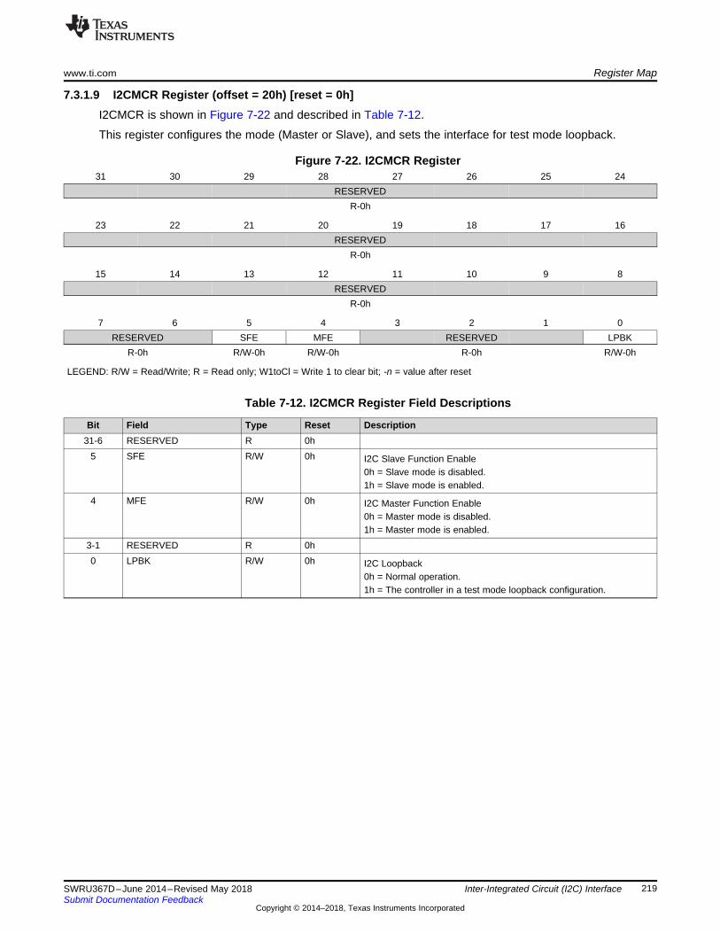
www.ti.com Register Map
219SWRU367D–June 2014–Revised May 2018Submit Documentation Feedback
Copyright © 2014–2018, Texas Instruments Incorporated
Inter-Integrated Circuit (I2C) Interface
7.3.1.9 I2CMCR Register (offset = 20h) [reset = 0h]I2CMCR is shown in Figure 7-22 and described in Table 7-12.
This register configures the mode (Master or Slave), and sets the interface for test mode loopback.
Figure 7-22. I2CMCR Register31 30 29 28 27 26 25 24
RESERVEDR-0h
23 22 21 20 19 18 17 16RESERVED
R-0h
15 14 13 12 11 10 9 8RESERVED
R-0h
7 6 5 4 3 2 1 0RESERVED SFE MFE RESERVED LPBK
R-0h R/W-0h R/W-0h R-0h R/W-0h
LEGEND: R/W = Read/Write; R = Read only; W1toCl = Write 1 to clear bit; -n = value after reset
Table 7-12. I2CMCR Register Field Descriptions
Bit Field Type Reset Description31-6 RESERVED R 0h
5 SFE R/W 0h I2C Slave Function Enable0h = Slave mode is disabled.1h = Slave mode is enabled.
4 MFE R/W 0h I2C Master Function Enable0h = Master mode is disabled.1h = Master mode is enabled.
3-1 RESERVED R 0h0 LPBK R/W 0h I2C Loopback
0h = Normal operation.1h = The controller in a test mode loopback configuration.

Register Map www.ti.com
220 SWRU367D–June 2014–Revised May 2018Submit Documentation Feedback
Copyright © 2014–2018, Texas Instruments Incorporated
Inter-Integrated Circuit (I2C) Interface
7.3.1.10 I2CMCLKOCNT Register (offset = 24h) [reset = 0h]I2CMCLKOCNT is shown in Figure 7-23 and described in Table 7-13.
This register contains the upper 8 bits of a 12-bit counter that can be used to keep the timeout limit forclock stretching by a remote slave. The lower four bits of the counter are not user visible and are always0x0.NOTE: The Master Clock Low Timeout counter counts for the entire time SCL is held Low continuously. IfSCL is de-asserted at any point, the Master Clock Low Timeout Counter is reloaded with the value in theI2CMCLKOCNT register and begins counting down from this value.
Figure 7-23. I2CMCLKOCNT Register31 30 29 28 27 26 25 24 23 22 21 20 19 18 17 16 15 14 13 12 11 10 9 8 7 6 5 4 3 2 1 0
RESERVED CNTLR-0h R/W-0h
LEGEND: R/W = Read/Write; R = Read only; W1toCl = Write 1 to clear bit; -n = value after reset
Table 7-13. I2CMCLKOCNT Register Field Descriptions
Bit Field Type Reset Description31-8 RESERVED R 0h7-0 CNTL R/W 0h I2C Master Count
This field contains the upper 8 bits of a 12-bit counter for the clocklow timeout count.Note: The value of CNTL must be greater than 0x1.
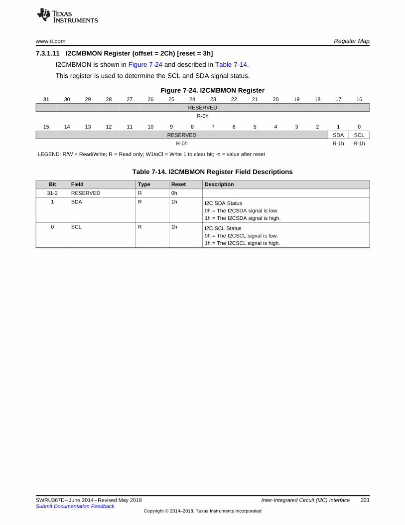
www.ti.com Register Map
221SWRU367D–June 2014–Revised May 2018Submit Documentation Feedback
Copyright © 2014–2018, Texas Instruments Incorporated
Inter-Integrated Circuit (I2C) Interface
7.3.1.11 I2CMBMON Register (offset = 2Ch) [reset = 3h]I2CMBMON is shown in Figure 7-24 and described in Table 7-14.
This register is used to determine the SCL and SDA signal status.
Figure 7-24. I2CMBMON Register31 30 29 28 27 26 25 24 23 22 21 20 19 18 17 16
RESERVEDR-0h
15 14 13 12 11 10 9 8 7 6 5 4 3 2 1 0RESERVED SDA SCL
R-0h R-1h R-1h
LEGEND: R/W = Read/Write; R = Read only; W1toCl = Write 1 to clear bit; -n = value after reset
Table 7-14. I2CMBMON Register Field Descriptions
Bit Field Type Reset Description31-2 RESERVED R 0h
1 SDA R 1h I2C SDA Status0h = The I2CSDA signal is low.1h = The I2CSDA signal is high.
0 SCL R 1h I2C SCL Status0h = The I2CSCL signal is low.1h = The I2CSCL signal is high.
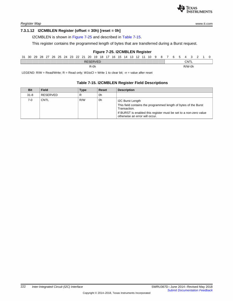
Register Map www.ti.com
222 SWRU367D–June 2014–Revised May 2018Submit Documentation Feedback
Copyright © 2014–2018, Texas Instruments Incorporated
Inter-Integrated Circuit (I2C) Interface
7.3.1.12 I2CMBLEN Register (offset = 30h) [reset = 0h]I2CMBLEN is shown in Figure 7-25 and described in Table 7-15.
This register contains the programmed length of bytes that are transferred during a Burst request.
Figure 7-25. I2CMBLEN Register31 30 29 28 27 26 25 24 23 22 21 20 19 18 17 16 15 14 13 12 11 10 9 8 7 6 5 4 3 2 1 0
RESERVED CNTLR-0h R/W-0h
LEGEND: R/W = Read/Write; R = Read only; W1toCl = Write 1 to clear bit; -n = value after reset
Table 7-15. I2CMBLEN Register Field Descriptions
Bit Field Type Reset Description31-8 RESERVED R 0h7-0 CNTL R/W 0h I2C Burst Length
This field contains the programmed length of bytes of the BurstTransaction.If BURST is enabled this register must be set to a non-zero valueotherwise an error will occur.
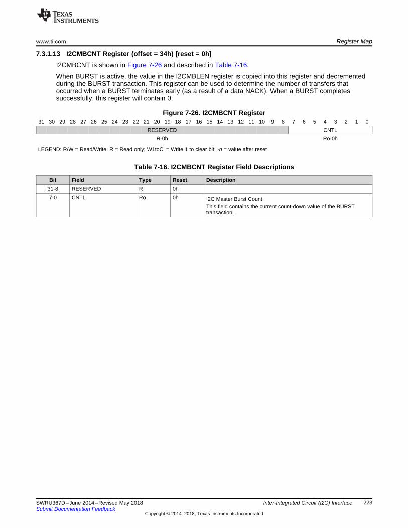
www.ti.com Register Map
223SWRU367D–June 2014–Revised May 2018Submit Documentation Feedback
Copyright © 2014–2018, Texas Instruments Incorporated
Inter-Integrated Circuit (I2C) Interface
7.3.1.13 I2CMBCNT Register (offset = 34h) [reset = 0h]I2CMBCNT is shown in Figure 7-26 and described in Table 7-16.
When BURST is active, the value in the I2CMBLEN register is copied into this register and decrementedduring the BURST transaction. This register can be used to determine the number of transfers thatoccurred when a BURST terminates early (as a result of a data NACK). When a BURST completessuccessfully, this register will contain 0.
Figure 7-26. I2CMBCNT Register31 30 29 28 27 26 25 24 23 22 21 20 19 18 17 16 15 14 13 12 11 10 9 8 7 6 5 4 3 2 1 0
RESERVED CNTLR-0h Ro-0h
LEGEND: R/W = Read/Write; R = Read only; W1toCl = Write 1 to clear bit; -n = value after reset
Table 7-16. I2CMBCNT Register Field Descriptions
Bit Field Type Reset Description31-8 RESERVED R 0h7-0 CNTL Ro 0h I2C Master Burst Count
This field contains the current count-down value of the BURSTtransaction.

Register Map www.ti.com
224 SWRU367D–June 2014–Revised May 2018Submit Documentation Feedback
Copyright © 2014–2018, Texas Instruments Incorporated
Inter-Integrated Circuit (I2C) Interface
7.3.1.14 I2CSOAR Register (offset = 800h) [reset = 0h]I2CSOAR is shown in Figure 7-27 and described in Table 7-17.
This register consists of seven address bits that identify the TM4E111BE6ZRB I2C device on the I2C bus.
Figure 7-27. I2CSOAR Register31 30 29 28 27 26 25 24 23 22 21 20 19 18 17 16 15 14 13 12 11 10 9 8 7 6 5 4 3 2 1 0
RESERVED OARR-0h R/W-0h
LEGEND: R/W = Read/Write; R = Read only; W1toCl = Write 1 to clear bit; -n = value after reset
Table 7-17. I2CSOAR Register Field Descriptions
Bit Field Type Reset Description31-7 RESERVED R 0h6-0 OAR R/W 0h I2C Slave Own Address
This field specifies bits A6 through A0 of the slave address.
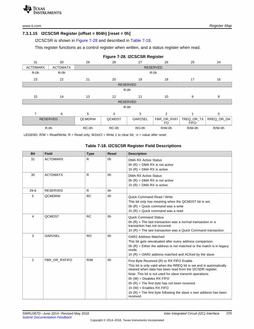
www.ti.com Register Map
225SWRU367D–June 2014–Revised May 2018Submit Documentation Feedback
Copyright © 2014–2018, Texas Instruments Incorporated
Inter-Integrated Circuit (I2C) Interface
7.3.1.15 I2CSCSR Register (offset = 804h) [reset = 0h]I2CSCSR is shown in Figure 7-28 and described in Table 7-18.
This register functions as a control register when written, and a status register when read.
Figure 7-28. I2CSCSR Register31 30 29 28 27 26 25 24
ACTDMARX ACTDMATX RESERVEDR-0h R-0h R-0h
23 22 21 20 19 18 17 16RESERVED
R-0h
15 14 13 12 11 10 9 8RESERVED
R-0h
7 6 5 4 3 2 1 0RESERVED QCMDRW QCMDST OAR2SEL FBR_OR_RXFI
FOTREQ_OR_TX
FIFORREQ_OR_DA
R-0h RC-0h RC-0h RO-0h R/W-0h R/W-0h R/W-0h
LEGEND: R/W = Read/Write; R = Read only; W1toCl = Write 1 to clear bit; -n = value after reset
Table 7-18. I2CSCSR Register Field Descriptions
Bit Field Type Reset Description31 ACTDMARX R 0h DMA RX Active Status
0h (R) = DMA RX is not active1h (R) = DMA RX is active.
30 ACTDMATX R 0h DMA RX Active Status0h (R) = DMA RX is not active1h (R) = DMA RX is active.
29-6 RESERVED R 0h5 QCMDRW RC 0h Quick Command Read / Write
This bit only has meaning when the QCMDST bit is set.0h (R) = Quick command was a write1h (R) = Quick command was a read
4 QCMDST RC 0h Quick Command Status0h (R) = The last transaction was a normal transaction or atransaction has not occurred.1h (R) = The last transaction was a Quick Command transaction.
3 OAR2SEL RO 0h OAR2 Address MatchedThis bit gets reevaluated after every address comparison.0h (R) = Either the address is not matched or the match is in legacymode.1h (R) = OAR2 address matched and ACKed by the slave.
2 FBR_OR_RXFIFO R/W 0h First Byte Received (R) or RX FIFO EnableThis bit is only valid when the RREQ bit is set and is automaticallycleared when data has been read from the I2CSDR register.Note: This bit is not used for slave transmit operations.0h (W) = Disables RX FIFO0h (R) = The first byte has not been received.1h (W) = Enables RX FIFO1h (R) = The first byte following the slave s own address has beenreceived.
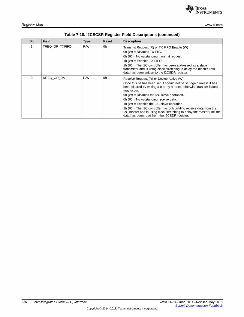
Register Map www.ti.com
226 SWRU367D–June 2014–Revised May 2018Submit Documentation Feedback
Copyright © 2014–2018, Texas Instruments Incorporated
Inter-Integrated Circuit (I2C) Interface
Table 7-18. I2CSCSR Register Field Descriptions (continued)Bit Field Type Reset Description1 TREQ_OR_TXFIFO R/W 0h Transmit Request (R) or TX FIFO Enable (W)
0h (W) = Disables TX FIFO0h (R) = No outstanding transmit request.1h (W) = Enables TX FIFO1h (R) = The I2C controller has been addressed as a slavetransmitter and is using clock stretching to delay the master untildata has been written to the I2CSDR register.
0 RREQ_OR_DA R/W 0h Receive Request (R) or Device Active (W)Once this bit has been set, it should not be set again unless it hasbeen cleared by writing a 0 or by a reset, otherwise transfer failuresmay occur.0h (W) = Disables the I2C slave operation.0h (R) = No outstanding receive data.1h (W) = Enables the I2C slave operation.1h (R) = The I2C controller has outstanding receive data from theI2C master and is using clock stretching to delay the master until thedata has been read from the I2CSDR register.
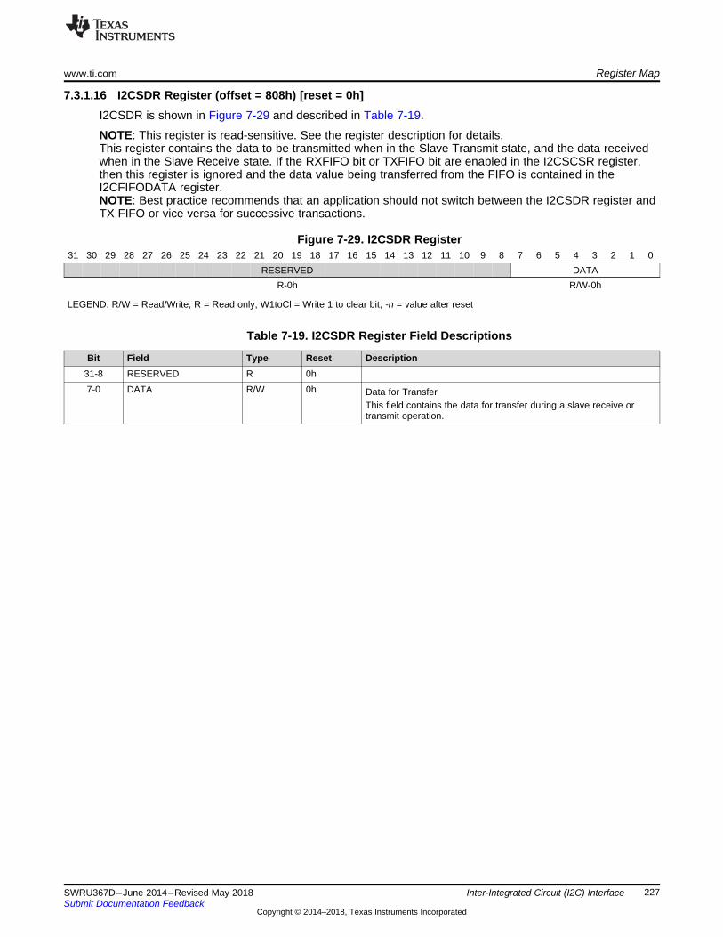
www.ti.com Register Map
227SWRU367D–June 2014–Revised May 2018Submit Documentation Feedback
Copyright © 2014–2018, Texas Instruments Incorporated
Inter-Integrated Circuit (I2C) Interface
7.3.1.16 I2CSDR Register (offset = 808h) [reset = 0h]I2CSDR is shown in Figure 7-29 and described in Table 7-19.
NOTE: This register is read-sensitive. See the register description for details.This register contains the data to be transmitted when in the Slave Transmit state, and the data receivedwhen in the Slave Receive state. If the RXFIFO bit or TXFIFO bit are enabled in the I2CSCSR register,then this register is ignored and the data value being transferred from the FIFO is contained in theI2CFIFODATA register.NOTE: Best practice recommends that an application should not switch between the I2CSDR register andTX FIFO or vice versa for successive transactions.
Figure 7-29. I2CSDR Register31 30 29 28 27 26 25 24 23 22 21 20 19 18 17 16 15 14 13 12 11 10 9 8 7 6 5 4 3 2 1 0
RESERVED DATAR-0h R/W-0h
LEGEND: R/W = Read/Write; R = Read only; W1toCl = Write 1 to clear bit; -n = value after reset
Table 7-19. I2CSDR Register Field Descriptions
Bit Field Type Reset Description31-8 RESERVED R 0h7-0 DATA R/W 0h Data for Transfer
This field contains the data for transfer during a slave receive ortransmit operation.
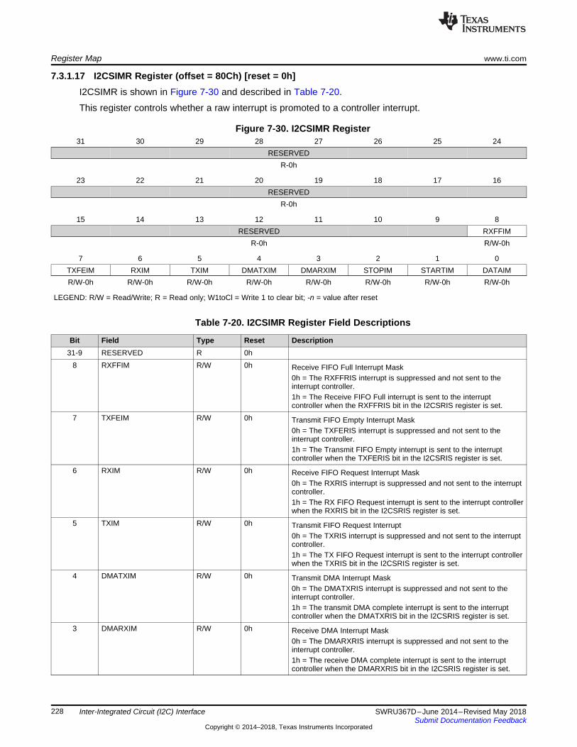
Register Map www.ti.com
228 SWRU367D–June 2014–Revised May 2018Submit Documentation Feedback
Copyright © 2014–2018, Texas Instruments Incorporated
Inter-Integrated Circuit (I2C) Interface
7.3.1.17 I2CSIMR Register (offset = 80Ch) [reset = 0h]I2CSIMR is shown in Figure 7-30 and described in Table 7-20.
This register controls whether a raw interrupt is promoted to a controller interrupt.
Figure 7-30. I2CSIMR Register31 30 29 28 27 26 25 24
RESERVEDR-0h
23 22 21 20 19 18 17 16RESERVED
R-0h
15 14 13 12 11 10 9 8RESERVED RXFFIM
R-0h R/W-0h
7 6 5 4 3 2 1 0TXFEIM RXIM TXIM DMATXIM DMARXIM STOPIM STARTIM DATAIMR/W-0h R/W-0h R/W-0h R/W-0h R/W-0h R/W-0h R/W-0h R/W-0h
LEGEND: R/W = Read/Write; R = Read only; W1toCl = Write 1 to clear bit; -n = value after reset
Table 7-20. I2CSIMR Register Field Descriptions
Bit Field Type Reset Description31-9 RESERVED R 0h
8 RXFFIM R/W 0h Receive FIFO Full Interrupt Mask0h = The RXFFRIS interrupt is suppressed and not sent to theinterrupt controller.1h = The Receive FIFO Full interrupt is sent to the interruptcontroller when the RXFFRIS bit in the I2CSRIS register is set.
7 TXFEIM R/W 0h Transmit FIFO Empty Interrupt Mask0h = The TXFERIS interrupt is suppressed and not sent to theinterrupt controller.1h = The Transmit FIFO Empty interrupt is sent to the interruptcontroller when the TXFERIS bit in the I2CSRIS register is set.
6 RXIM R/W 0h Receive FIFO Request Interrupt Mask0h = The RXRIS interrupt is suppressed and not sent to the interruptcontroller.1h = The RX FIFO Request interrupt is sent to the interrupt controllerwhen the RXRIS bit in the I2CSRIS register is set.
5 TXIM R/W 0h Transmit FIFO Request Interrupt0h = The TXRIS interrupt is suppressed and not sent to the interruptcontroller.1h = The TX FIFO Request interrupt is sent to the interrupt controllerwhen the TXRIS bit in the I2CSRIS register is set.
4 DMATXIM R/W 0h Transmit DMA Interrupt Mask0h = The DMATXRIS interrupt is suppressed and not sent to theinterrupt controller.1h = The transmit DMA complete interrupt is sent to the interruptcontroller when the DMATXRIS bit in the I2CSRIS register is set.
3 DMARXIM R/W 0h Receive DMA Interrupt Mask0h = The DMARXRIS interrupt is suppressed and not sent to theinterrupt controller.1h = The receive DMA complete interrupt is sent to the interruptcontroller when the DMARXRIS bit in the I2CSRIS register is set.

www.ti.com Register Map
229SWRU367D–June 2014–Revised May 2018Submit Documentation Feedback
Copyright © 2014–2018, Texas Instruments Incorporated
Inter-Integrated Circuit (I2C) Interface
Table 7-20. I2CSIMR Register Field Descriptions (continued)Bit Field Type Reset Description2 STOPIM R/W 0h Stop Condition Interrupt Mask
0h = The STOPRIS interrupt is suppressed and not sent to theinterrupt controller.1h = The STOP condition interrupt is sent to the interrupt controllerwhen the STOPRIS bit in the I2CSRIS register is set.
1 STARTIM R/W 0h Start Condition Interrupt Mask0h = The STARTRIS interrupt is suppressed and not sent to theinterrupt controller.1h = The START condition interrupt is sent to the interrupt controllerwhen the STARTRIS bit in the I2CSRIS register is set.
0 DATAIM R/W 0h Data Interrupt Mask0h = The DATARIS interrupt is suppressed and not sent to theinterrupt controller.1h = Data interrupt sent to interrupt controller when DATARIS bit inthe I2CSRIS register is set.
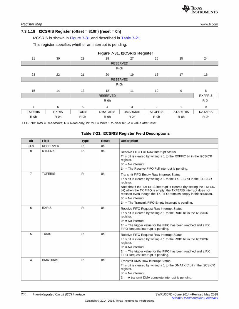
Register Map www.ti.com
230 SWRU367D–June 2014–Revised May 2018Submit Documentation Feedback
Copyright © 2014–2018, Texas Instruments Incorporated
Inter-Integrated Circuit (I2C) Interface
7.3.1.18 I2CSRIS Register (offset = 810h) [reset = 0h]I2CSRIS is shown in Figure 7-31 and described in Table 7-21.
This register specifies whether an interrupt is pending.
Figure 7-31. I2CSRIS Register31 30 29 28 27 26 25 24
RESERVEDR-0h
23 22 21 20 19 18 17 16RESERVED
R-0h
15 14 13 12 11 10 9 8RESERVED RXFFRIS
R-0h R-0h
7 6 5 4 3 2 1 0TXFERIS RXRIS TXRIS DMATXRIS DMARXRIS STOPRIS STARTRIS DATARIS
R-0h R-0h R-0h R-0h R-0h R-0h R-0h R-0h
LEGEND: R/W = Read/Write; R = Read only; W1toCl = Write 1 to clear bit; -n = value after reset
Table 7-21. I2CSRIS Register Field Descriptions
Bit Field Type Reset Description31-9 RESERVED R 0h
8 RXFFRIS R 0h Receive FIFO Full Raw Interrupt StatusThis bit is cleared by writing a 1 to the RXFFIC bit in the I2CSICRregister.0h = No interrupt1h = The Receive FIFO Full interrupt is pending.
7 TXFERIS R 0h Transmit FIFO Empty Raw Interrupt StatusThis bit is cleared by writing a 1 to the TXFEIC bit in the I2CSICRregister.Note that if the TXFERIS interrupt is cleared (by setting the TXFEICbit) when the TX FIFO is empty, the TXFERIS interrupt does notreassert even though the TX FIFO remains empty in this situation.0h = No interrupt1h = The Transmit FIFO Empty interrupt is pending.
6 RXRIS R 0h Receive FIFO Request Raw Interrupt StatusThis bit is cleared by writing a 1 to the RXIC bit in the I2CSICRregister.0h = No interrupt1h = The trigger value for the FIFO has been reached and a RXFIFO Request interrupt is pending.
5 TXRIS R 0h Receive FIFO Request Raw Interrupt StatusThis bit is cleared by writing a 1 to the RXIC bit in the I2CSICRregister.0h = No interrupt1h = The trigger value for the FIFO has been reached and a RXFIFO Request interrupt is pending.
4 DMATXRIS R 0h Transmit DMA Raw Interrupt StatusThis bit is cleared by writing a 1 to the DMATXIC bit in the I2CSICRregister.0h = No interrupt1h = A transmit DMA complete interrupt is pending.
www.ti.com Register Map
231SWRU367D–June 2014–Revised May 2018Submit Documentation Feedback
Copyright © 2014–2018, Texas Instruments Incorporated
Inter-Integrated Circuit (I2C) Interface
Table 7-21. I2CSRIS Register Field Descriptions (continued)Bit Field Type Reset Description3 DMARXRIS R 0h Receive DMA Raw Interrupt Status
This bit is cleared by writing a 1 to the DMARXIC bit in the I2CSICRregister.0h = No interrupt1h = A receive DMA complete interrupt is pending.
2 STOPRIS R 0h Stop Condition Raw Interrupt StatusThis bit is cleared by writing a 1 to the STOPIC bit in the I2CSICRregister.0h = No interrupt1h = A STOP condition interrupt is pending.
1 STARTRIS R 0h Start Condition Raw Interrupt StatusThis bit is cleared by writing a 1 to the STARTIC bit in the I2CSICRregister.0h = No interrupt.1h = A START condition interrupt is pending.
0 DATARIS R 0h Data Raw Interrupt StatusThis interrupt encompasses the following: Slave transaction receivedSlave transaction requestedNext byte transfer requestThis bit is cleared by writing a 1 to the DATAIC bit in the I2CSICRregister.0h = No interrupt.1h = Slave Interrupt is pending.
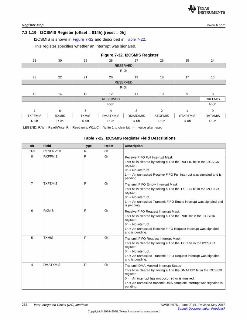
Register Map www.ti.com
232 SWRU367D–June 2014–Revised May 2018Submit Documentation Feedback
Copyright © 2014–2018, Texas Instruments Incorporated
Inter-Integrated Circuit (I2C) Interface
7.3.1.19 I2CSMIS Register (offset = 814h) [reset = 0h]I2CSMIS is shown in Figure 7-32 and described in Table 7-22.
This register specifies whether an interrupt was signaled.
Figure 7-32. I2CSMIS Register31 30 29 28 27 26 25 24
RESERVEDR-0h
23 22 21 20 19 18 17 16RESERVED
R-0h
15 14 13 12 11 10 9 8RESERVED RXFFMIS
R-0h R-0h
7 6 5 4 3 2 1 0TXFEMIS RXMIS TXMIS DMATXMIS DMARXMIS STOPMIS STARTMIS DATAMIS
R-0h R-0h R-0h R-0h R-0h R-0h R-0h R-0h
LEGEND: R/W = Read/Write; R = Read only; W1toCl = Write 1 to clear bit; -n = value after reset
Table 7-22. I2CSMIS Register Field Descriptions
Bit Field Type Reset Description31-9 RESERVED R 0h
8 RXFFMIS R 0h Receive FIFO Full Interrupt MaskThis bit is cleared by writing a 1 to the RXFFIC bit in the I2CSICRregister.0h = No interrupt.1h = An unmasked Receive FIFO Full interrupt was signaled and ispending.
7 TXFEMIS R 0h Transmit FIFO Empty Interrupt MaskThis bit is cleared by writing a 1 to the TXFEIC bit in the I2CSICRregister.0h = No interrupt.1h = An unmasked Transmit FIFO Empty interrupt was signaled andis pending.
6 RXMIS R 0h Receive FIFO Request Interrupt MaskThis bit is cleared by writing a 1 to the RXIC bit in the I2CSICRregister.0h = No interrupt.1h = An unmasked Receive FIFO Request interrupt was signaledand is pending.
5 TXMIS R 0h Transmit FIFO Request Interrupt MaskThis bit is cleared by writing a 1 to the TXIC bit in the I2CSICRregister.0h = No interrupt.1h = An unmasked Transmit FIFO Request interrupt was signaledand is pending.
4 DMATXMIS R 0h Transmit DMA Masked Interrupt StatusThis bit is cleared by writing a 1 to the DMATXIC bit in the I2CSICRregister.0h = An interrupt has not occurred or is masked.1h = An unmasked transmit DMA complete interrupt was signaled ispending.
www.ti.com Register Map
233SWRU367D–June 2014–Revised May 2018Submit Documentation Feedback
Copyright © 2014–2018, Texas Instruments Incorporated
Inter-Integrated Circuit (I2C) Interface
Table 7-22. I2CSMIS Register Field Descriptions (continued)Bit Field Type Reset Description3 DMARXMIS R 0h Receive DMA Masked Interrupt Status
This bit is cleared by writing a 1 to the DMARXIC bit in the I2CSICRregister.0h = An interrupt has not occurred or is masked.1h = An unmasked receive DMA complete interrupt was signaled ispending.
2 STOPMIS R 0h Stop Condition Masked Interrupt StatusThis bit is cleared by writing a 1 to the STOPIC bit in the I2CSICRregister.0h = An interrupt has not occurred or is masked.1h = An unmasked STOP condition interrupt was signaled ispending.
1 STARTMIS R 0h Start Condition Masked Interrupt StatusThis bit is cleared by writing a 1 to the STARTIC bit in the I2CSICRregister.0h = An interrupt has not occurred or is masked.1h = An unmasked START condition interrupt was signaled ispending.
0 DATAMIS R 0h Data Masked Interrupt StatusThis bit is cleared by writing a 1 to the DATAIC bit in the I2CSICRregister.0h = An interrupt has not occurred or is masked.1h = An unmasked slave data interrupt was signaled is pending.
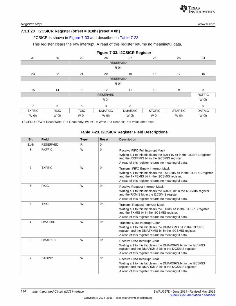
Register Map www.ti.com
234 SWRU367D–June 2014–Revised May 2018Submit Documentation Feedback
Copyright © 2014–2018, Texas Instruments Incorporated
Inter-Integrated Circuit (I2C) Interface
7.3.1.20 I2CSICR Register (offset = 818h) [reset = 0h]I2CSICR is shown in Figure 7-33 and described in Table 7-23.
This register clears the raw interrupt. A read of this register returns no meaningful data.
Figure 7-33. I2CSICR Register31 30 29 28 27 26 25 24
RESERVEDR-0h
23 22 21 20 19 18 17 16RESERVED
R-0h
15 14 13 12 11 10 9 8RESERVED RXFFIC
R-0h W-0h
7 6 5 4 3 2 1 0TXFEIC RXIC TXIC DMATXIC DMARXIC STOPIC STARTIC DATAIC
W-0h W-0h W-0h W-0h W-0h W-0h W-0h W-0h
LEGEND: R/W = Read/Write; R = Read only; W1toCl = Write 1 to clear bit; -n = value after reset
Table 7-23. I2CSICR Register Field Descriptions
Bit Field Type Reset Description31-9 RESERVED R 0h
8 RXFFIC W 0h Receive FIFO Full Interrupt MaskWriting a 1 to this bit clears the RXFFIS bit in the I2CSRIS registerand the RXFFMIS bit in the I2CSMIS register.A read of this register returns no meaningful data.
7 TXFEIC W 0h Transmit FIFO Empty Interrupt MaskWriting a 1 to this bit clears the TXFERIS bit in the I2CSRIS registerand the TXFEMIS bit in the I2CSMIS register.A read of this register returns no meaningful data.
6 RXIC W 0h Receive Request Interrupt MaskWriting a 1 to this bit clears the RXRIS bit in the I2CSRIS registerand the RXMIS bit in the I2CSMIS register.A read of this register returns no meaningful data.
5 TXIC W 0h Transmit Request Interrupt MaskWriting a 1 to this bit clears the TXRIS bit in the I2CSRIS registerand the TXMIS bit in the I2CSMIS register.A read of this register returns no meaningful data.
4 DMATXIC W 0h Transmit DMA Interrupt ClearWriting a 1 to this bit clears the DMATXRIS bit in the I2CSRISregister and the DMATXMIS bit in the I2CSMIS register.A read of this register returns no meaningful data.
3 DMARXIC W 0h Receive DMA Interrupt ClearWriting a 1 to this bit clears the DMARXRIS bit in the I2CSRISregister and the DMARXMIS bit in the I2CSMIS register.A read of this register returns no meaningful data.
2 STOPIC W 0h Receive DMA Interrupt ClearWriting a 1 to this bit clears the DMARXRIS bit in the I2CSRISregister and the DMARXMIS bit in the I2CSMIS register.A read of this register returns no meaningful data.
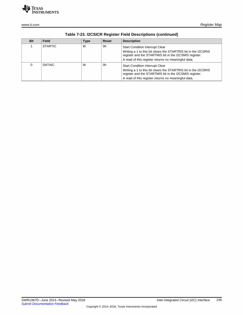
www.ti.com Register Map
235SWRU367D–June 2014–Revised May 2018Submit Documentation Feedback
Copyright © 2014–2018, Texas Instruments Incorporated
Inter-Integrated Circuit (I2C) Interface
Table 7-23. I2CSICR Register Field Descriptions (continued)Bit Field Type Reset Description1 STARTIC W 0h Start Condition Interrupt Clear
Writing a 1 to this bit clears the STARTRIS bit in the I2CSRISregister and the STARTMIS bit in the I2CSMIS register.A read of this register returns no meaningful data.
0 DATAIC W 0h Start Condition Interrupt ClearWriting a 1 to this bit clears the STARTRIS bit in the I2CSRISregister and the STARTMIS bit in the I2CSMIS register.A read of this register returns no meaningful data.
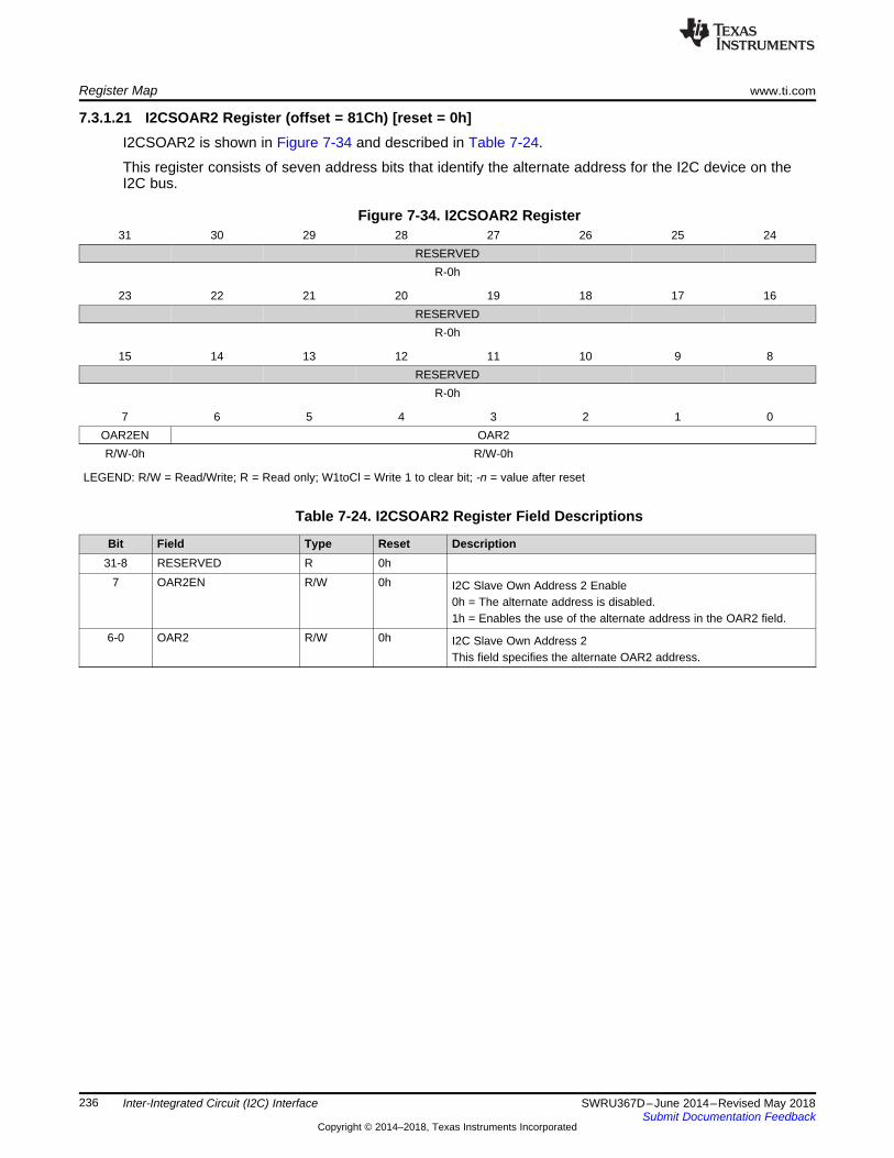
Register Map www.ti.com
236 SWRU367D–June 2014–Revised May 2018Submit Documentation Feedback
Copyright © 2014–2018, Texas Instruments Incorporated
Inter-Integrated Circuit (I2C) Interface
7.3.1.21 I2CSOAR2 Register (offset = 81Ch) [reset = 0h]I2CSOAR2 is shown in Figure 7-34 and described in Table 7-24.
This register consists of seven address bits that identify the alternate address for the I2C device on theI2C bus.
Figure 7-34. I2CSOAR2 Register31 30 29 28 27 26 25 24
RESERVEDR-0h
23 22 21 20 19 18 17 16RESERVED
R-0h
15 14 13 12 11 10 9 8RESERVED
R-0h
7 6 5 4 3 2 1 0OAR2EN OAR2R/W-0h R/W-0h
LEGEND: R/W = Read/Write; R = Read only; W1toCl = Write 1 to clear bit; -n = value after reset
Table 7-24. I2CSOAR2 Register Field Descriptions
Bit Field Type Reset Description31-8 RESERVED R 0h
7 OAR2EN R/W 0h I2C Slave Own Address 2 Enable0h = The alternate address is disabled.1h = Enables the use of the alternate address in the OAR2 field.
6-0 OAR2 R/W 0h I2C Slave Own Address 2This field specifies the alternate OAR2 address.
www.ti.com Register Map
237SWRU367D–June 2014–Revised May 2018Submit Documentation Feedback
Copyright © 2014–2018, Texas Instruments Incorporated
Inter-Integrated Circuit (I2C) Interface
7.3.1.22 I2CSACKCTL Register (offset = 820h) [reset = 0h]I2CSACKCTL is shown in Figure 7-35 and described in Table 7-25.
This register enables the I2C slave to NACK for invalid data or command or ACK for valid data orcommand. The I2C clock is pulled low after the last data bit until this register is written.
Figure 7-35. I2CSACKCTL Register31 30 29 28 27 26 25 24
RESERVEDR-0h
23 22 21 20 19 18 17 16RESERVED
R-0h
15 14 13 12 11 10 9 8RESERVED
R-0h
7 6 5 4 3 2 1 0RESERVED ACKOVAL ACKOEN
R-0h R/W-0h R/W-0h
LEGEND: R/W = Read/Write; R = Read only; W1toCl = Write 1 to clear bit; -n = value after reset
Table 7-25. I2CSACKCTL Register Field Descriptions
Bit Field Type Reset Description31-2 RESERVED R 0h
1 ACKOVAL R/W 0h I2C Slave ACK Override Value0h = An ACK is sent indicating valid data or command.1h = A NACK is sent indicating invalid data or command.
0 ACKOEN R/W 0h I2C Slave ACK Override Enable0h = A response in not provided.1h = An ACK or NACK is sent according to the value written to theACKOVAL bit.
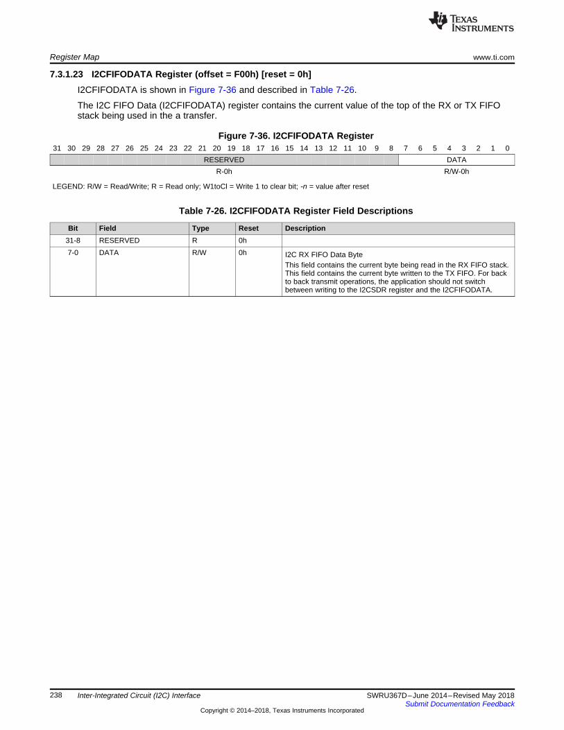
Register Map www.ti.com
238 SWRU367D–June 2014–Revised May 2018Submit Documentation Feedback
Copyright © 2014–2018, Texas Instruments Incorporated
Inter-Integrated Circuit (I2C) Interface
7.3.1.23 I2CFIFODATA Register (offset = F00h) [reset = 0h]I2CFIFODATA is shown in Figure 7-36 and described in Table 7-26.
The I2C FIFO Data (I2CFIFODATA) register contains the current value of the top of the RX or TX FIFOstack being used in the a transfer.
Figure 7-36. I2CFIFODATA Register31 30 29 28 27 26 25 24 23 22 21 20 19 18 17 16 15 14 13 12 11 10 9 8 7 6 5 4 3 2 1 0
RESERVED DATAR-0h R/W-0h
LEGEND: R/W = Read/Write; R = Read only; W1toCl = Write 1 to clear bit; -n = value after reset
Table 7-26. I2CFIFODATA Register Field Descriptions
Bit Field Type Reset Description31-8 RESERVED R 0h7-0 DATA R/W 0h I2C RX FIFO Data Byte
This field contains the current byte being read in the RX FIFO stack.This field contains the current byte written to the TX FIFO. For backto back transmit operations, the application should not switchbetween writing to the I2CSDR register and the I2CFIFODATA.
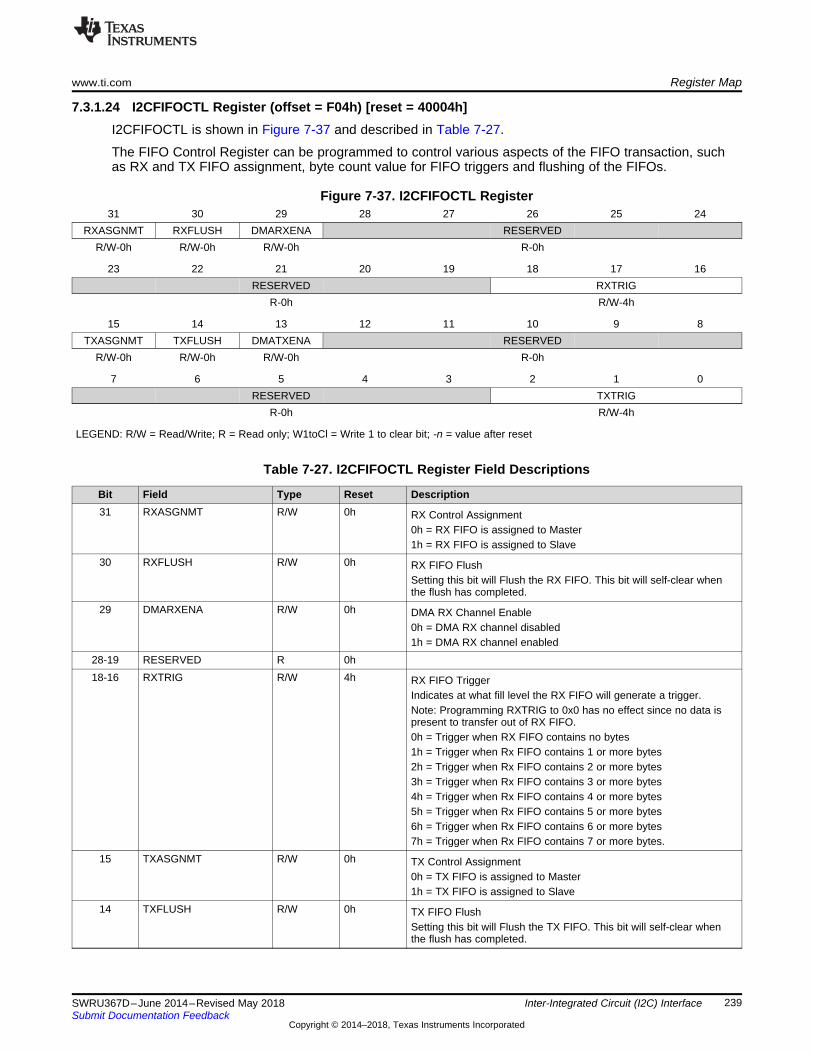
www.ti.com Register Map
239SWRU367D–June 2014–Revised May 2018Submit Documentation Feedback
Copyright © 2014–2018, Texas Instruments Incorporated
Inter-Integrated Circuit (I2C) Interface
7.3.1.24 I2CFIFOCTL Register (offset = F04h) [reset = 40004h]I2CFIFOCTL is shown in Figure 7-37 and described in Table 7-27.
The FIFO Control Register can be programmed to control various aspects of the FIFO transaction, suchas RX and TX FIFO assignment, byte count value for FIFO triggers and flushing of the FIFOs.
Figure 7-37. I2CFIFOCTL Register31 30 29 28 27 26 25 24
RXASGNMT RXFLUSH DMARXENA RESERVEDR/W-0h R/W-0h R/W-0h R-0h
23 22 21 20 19 18 17 16RESERVED RXTRIG
R-0h R/W-4h
15 14 13 12 11 10 9 8TXASGNMT TXFLUSH DMATXENA RESERVED
R/W-0h R/W-0h R/W-0h R-0h
7 6 5 4 3 2 1 0RESERVED TXTRIG
R-0h R/W-4h
LEGEND: R/W = Read/Write; R = Read only; W1toCl = Write 1 to clear bit; -n = value after reset
Table 7-27. I2CFIFOCTL Register Field Descriptions
Bit Field Type Reset Description31 RXASGNMT R/W 0h RX Control Assignment
0h = RX FIFO is assigned to Master1h = RX FIFO is assigned to Slave
30 RXFLUSH R/W 0h RX FIFO FlushSetting this bit will Flush the RX FIFO. This bit will self-clear whenthe flush has completed.
29 DMARXENA R/W 0h DMA RX Channel Enable0h = DMA RX channel disabled1h = DMA RX channel enabled
28-19 RESERVED R 0h18-16 RXTRIG R/W 4h RX FIFO Trigger
Indicates at what fill level the RX FIFO will generate a trigger.Note: Programming RXTRIG to 0x0 has no effect since no data ispresent to transfer out of RX FIFO.0h = Trigger when RX FIFO contains no bytes1h = Trigger when Rx FIFO contains 1 or more bytes2h = Trigger when Rx FIFO contains 2 or more bytes3h = Trigger when Rx FIFO contains 3 or more bytes4h = Trigger when Rx FIFO contains 4 or more bytes5h = Trigger when Rx FIFO contains 5 or more bytes6h = Trigger when Rx FIFO contains 6 or more bytes7h = Trigger when Rx FIFO contains 7 or more bytes.
15 TXASGNMT R/W 0h TX Control Assignment0h = TX FIFO is assigned to Master1h = TX FIFO is assigned to Slave
14 TXFLUSH R/W 0h TX FIFO FlushSetting this bit will Flush the TX FIFO. This bit will self-clear whenthe flush has completed.
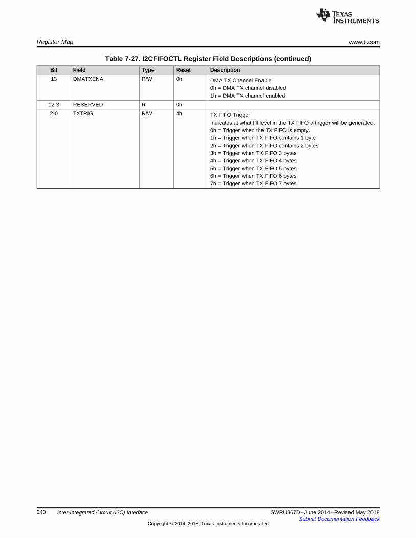
Register Map www.ti.com
240 SWRU367D–June 2014–Revised May 2018Submit Documentation Feedback
Copyright © 2014–2018, Texas Instruments Incorporated
Inter-Integrated Circuit (I2C) Interface
Table 7-27. I2CFIFOCTL Register Field Descriptions (continued)Bit Field Type Reset Description13 DMATXENA R/W 0h DMA TX Channel Enable
0h = DMA TX channel disabled1h = DMA TX channel enabled
12-3 RESERVED R 0h2-0 TXTRIG R/W 4h TX FIFO Trigger
Indicates at what fill level in the TX FIFO a trigger will be generated.0h = Trigger when the TX FIFO is empty.1h = Trigger when TX FIFO contains 1 byte2h = Trigger when TX FIFO contains 2 bytes3h = Trigger when TX FIFO 3 bytes4h = Trigger when TX FIFO 4 bytes5h = Trigger when TX FIFO 5 bytes6h = Trigger when TX FIFO 6 bytes7h = Trigger when TX FIFO 7 bytes
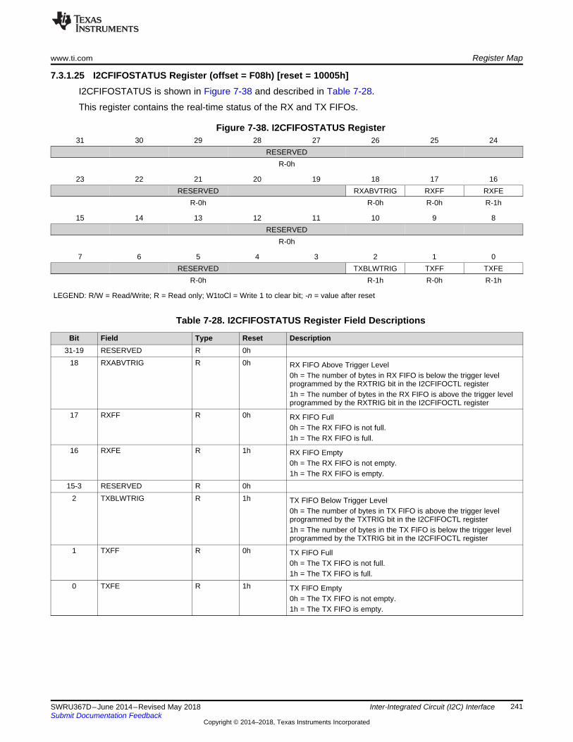
www.ti.com Register Map
241SWRU367D–June 2014–Revised May 2018Submit Documentation Feedback
Copyright © 2014–2018, Texas Instruments Incorporated
Inter-Integrated Circuit (I2C) Interface
7.3.1.25 I2CFIFOSTATUS Register (offset = F08h) [reset = 10005h]I2CFIFOSTATUS is shown in Figure 7-38 and described in Table 7-28.
This register contains the real-time status of the RX and TX FIFOs.
Figure 7-38. I2CFIFOSTATUS Register31 30 29 28 27 26 25 24
RESERVEDR-0h
23 22 21 20 19 18 17 16RESERVED RXABVTRIG RXFF RXFE
R-0h R-0h R-0h R-1h
15 14 13 12 11 10 9 8RESERVED
R-0h
7 6 5 4 3 2 1 0RESERVED TXBLWTRIG TXFF TXFE
R-0h R-1h R-0h R-1h
LEGEND: R/W = Read/Write; R = Read only; W1toCl = Write 1 to clear bit; -n = value after reset
Table 7-28. I2CFIFOSTATUS Register Field Descriptions
Bit Field Type Reset Description31-19 RESERVED R 0h
18 RXABVTRIG R 0h RX FIFO Above Trigger Level0h = The number of bytes in RX FIFO is below the trigger levelprogrammed by the RXTRIG bit in the I2CFIFOCTL register1h = The number of bytes in the RX FIFO is above the trigger levelprogrammed by the RXTRIG bit in the I2CFIFOCTL register
17 RXFF R 0h RX FIFO Full0h = The RX FIFO is not full.1h = The RX FIFO is full.
16 RXFE R 1h RX FIFO Empty0h = The RX FIFO is not empty.1h = The RX FIFO is empty.
15-3 RESERVED R 0h2 TXBLWTRIG R 1h TX FIFO Below Trigger Level
0h = The number of bytes in TX FIFO is above the trigger levelprogrammed by the TXTRIG bit in the I2CFIFOCTL register1h = The number of bytes in the TX FIFO is below the trigger levelprogrammed by the TXTRIG bit in the I2CFIFOCTL register
1 TXFF R 0h TX FIFO Full0h = The TX FIFO is not full.1h = The TX FIFO is full.
0 TXFE R 1h TX FIFO Empty0h = The TX FIFO is not empty.1h = The TX FIFO is empty.
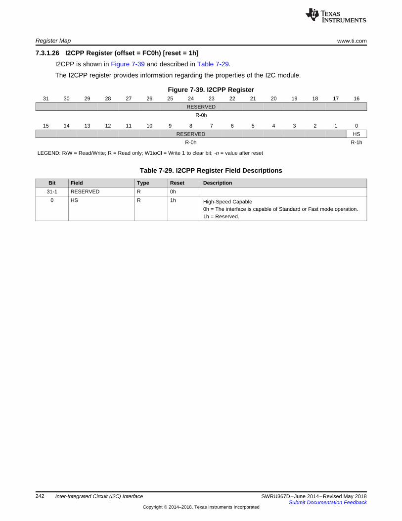
Register Map www.ti.com
242 SWRU367D–June 2014–Revised May 2018Submit Documentation Feedback
Copyright © 2014–2018, Texas Instruments Incorporated
Inter-Integrated Circuit (I2C) Interface
7.3.1.26 I2CPP Register (offset = FC0h) [reset = 1h]I2CPP is shown in Figure 7-39 and described in Table 7-29.
The I2CPP register provides information regarding the properties of the I2C module.
Figure 7-39. I2CPP Register31 30 29 28 27 26 25 24 23 22 21 20 19 18 17 16
RESERVEDR-0h
15 14 13 12 11 10 9 8 7 6 5 4 3 2 1 0RESERVED HS
R-0h R-1h
LEGEND: R/W = Read/Write; R = Read only; W1toCl = Write 1 to clear bit; -n = value after reset
Table 7-29. I2CPP Register Field Descriptions
Bit Field Type Reset Description31-1 RESERVED R 0h
0 HS R 1h High-Speed Capable0h = The interface is capable of Standard or Fast mode operation.1h = Reserved.
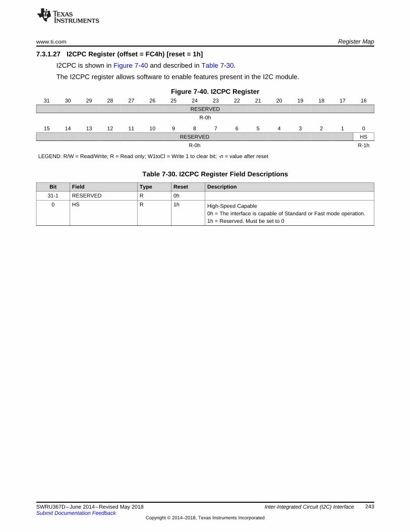
www.ti.com Register Map
243SWRU367D–June 2014–Revised May 2018Submit Documentation Feedback
Copyright © 2014–2018, Texas Instruments Incorporated
Inter-Integrated Circuit (I2C) Interface
7.3.1.27 I2CPC Register (offset = FC4h) [reset = 1h]I2CPC is shown in Figure 7-40 and described in Table 7-30.
The I2CPC register allows software to enable features present in the I2C module.
Figure 7-40. I2CPC Register31 30 29 28 27 26 25 24 23 22 21 20 19 18 17 16
RESERVEDR-0h
15 14 13 12 11 10 9 8 7 6 5 4 3 2 1 0RESERVED HS
R-0h R-1h
LEGEND: R/W = Read/Write; R = Read only; W1toCl = Write 1 to clear bit; -n = value after reset
Table 7-30. I2CPC Register Field Descriptions
Bit Field Type Reset Description31-1 RESERVED R 0h
0 HS R 1h High-Speed Capable0h = The interface is capable of Standard or Fast mode operation.1h = Reserved. Must be set to 0
244 SWRU367D–June 2014–Revised May 2018Submit Documentation Feedback
Copyright © 2014–2018, Texas Instruments Incorporated
SPI (Serial Peripheral Interface)
Chapter 8SWRU367D–June 2014–Revised May 2018
SPI (Serial Peripheral Interface)
Topic ........................................................................................................................... Page
8.1 Overview ......................................................................................................... 2458.2 Functional Description ...................................................................................... 2468.3 Initialization and Configuration .......................................................................... 2618.4 Access to Data Registers .................................................................................. 2628.5 Module Initialization .......................................................................................... 2638.6 SPI Registers ................................................................................................... 269
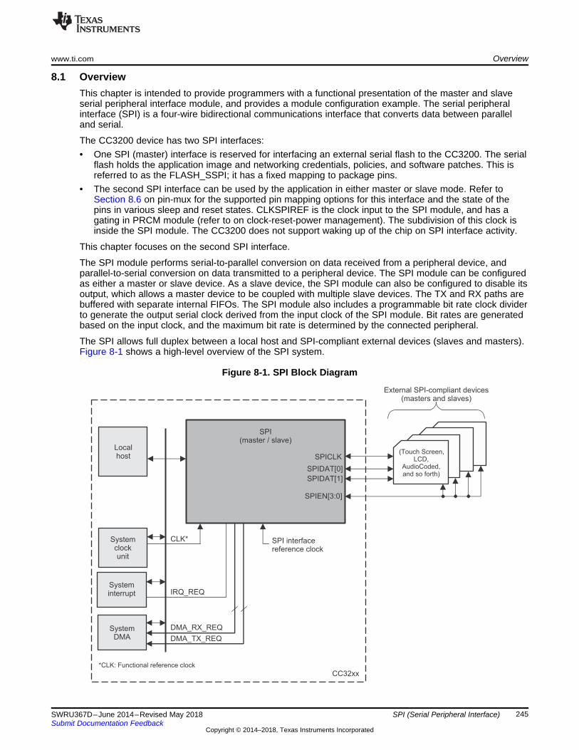
www.ti.com Overview
245SWRU367D–June 2014–Revised May 2018Submit Documentation Feedback
Copyright © 2014–2018, Texas Instruments Incorporated
SPI (Serial Peripheral Interface)
8.1 OverviewThis chapter is intended to provide programmers with a functional presentation of the master and slaveserial peripheral interface module, and provides a module configuration example. The serial peripheralinterface (SPI) is a four-wire bidirectional communications interface that converts data between paralleland serial.
The CC3200 device has two SPI interfaces:• One SPI (master) interface is reserved for interfacing an external serial flash to the CC3200. The serial
flash holds the application image and networking credentials, policies, and software patches. This isreferred to as the FLASH_SSPI; it has a fixed mapping to package pins.
• The second SPI interface can be used by the application in either master or slave mode. Refer toSection 8.6 on pin-mux for the supported pin mapping options for this interface and the state of thepins in various sleep and reset states. CLKSPIREF is the clock input to the SPI module, and has agating in PRCM module (refer to on clock-reset-power management). The subdivision of this clock isinside the SPI module. The CC3200 does not support waking up of the chip on SPI interface activity.
This chapter focuses on the second SPI interface.
The SPI module performs serial-to-parallel conversion on data received from a peripheral device, andparallel-to-serial conversion on data transmitted to a peripheral device. The SPI module can be configuredas either a master or slave device. As a slave device, the SPI module can also be configured to disable itsoutput, which allows a master device to be coupled with multiple slave devices. The TX and RX paths arebuffered with separate internal FIFOs. The SPI module also includes a programmable bit rate clock dividerto generate the output serial clock derived from the input clock of the SPI module. Bit rates are generatedbased on the input clock, and the maximum bit rate is determined by the connected peripheral.
The SPI allows full duplex between a local host and SPI-compliant external devices (slaves and masters).Figure 8-1 shows a high-level overview of the SPI system.
Figure 8-1. SPI Block Diagram
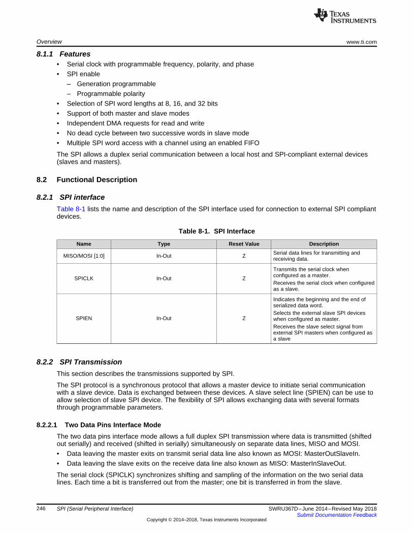
Overview www.ti.com
246 SWRU367D–June 2014–Revised May 2018Submit Documentation Feedback
Copyright © 2014–2018, Texas Instruments Incorporated
SPI (Serial Peripheral Interface)
8.1.1 Features• Serial clock with programmable frequency, polarity, and phase• SPI enable
– Generation programmable– Programmable polarity
• Selection of SPI word lengths at 8, 16, and 32 bits• Support of both master and slave modes• Independent DMA requests for read and write• No dead cycle between two successive words in slave mode• Multiple SPI word access with a channel using an enabled FIFO
The SPI allows a duplex serial communication between a local host and SPI-compliant external devices(slaves and masters).
8.2 Functional Description
8.2.1 SPI interfaceTable 8-1 lists the name and description of the SPI interface used for connection to external SPI compliantdevices.
Table 8-1. SPI Interface
Name Type Reset Value Description
MISO/MOSI [1:0] In-Out Z Serial data lines for transmitting andreceiving data.
SPICLK In-Out Z
Transmits the serial clock whenconfigured as a master.Receives the serial clock when configuredas a slave.
SPIEN In-Out Z
Indicates the beginning and the end ofserialized data word.Selects the external slave SPI deviceswhen configured as master.Receives the slave select signal fromexternal SPI masters when configured asa slave
8.2.2 SPI TransmissionThis section describes the transmissions supported by SPI.
The SPI protocol is a synchronous protocol that allows a master device to initiate serial communicationwith a slave device. Data is exchanged between these devices. A slave select line (SPIEN) can be use toallow selection of slave SPI device. The flexibility of SPI allows exchanging data with several formatsthrough programmable parameters.
8.2.2.1 Two Data Pins Interface ModeThe two data pins interface mode allows a full duplex SPI transmission where data is transmitted (shiftedout serially) and received (shifted in serially) simultaneously on separate data lines, MISO and MOSI.• Data leaving the master exits on transmit serial data line also known as MOSI: MasterOutSlaveIn.• Data leaving the slave exits on the receive data line also known as MISO: MasterInSlaveOut.
The serial clock (SPICLK) synchronizes shifting and sampling of the information on the two serial datalines. Each time a bit is transferred out from the master; one bit is transferred in from the slave.
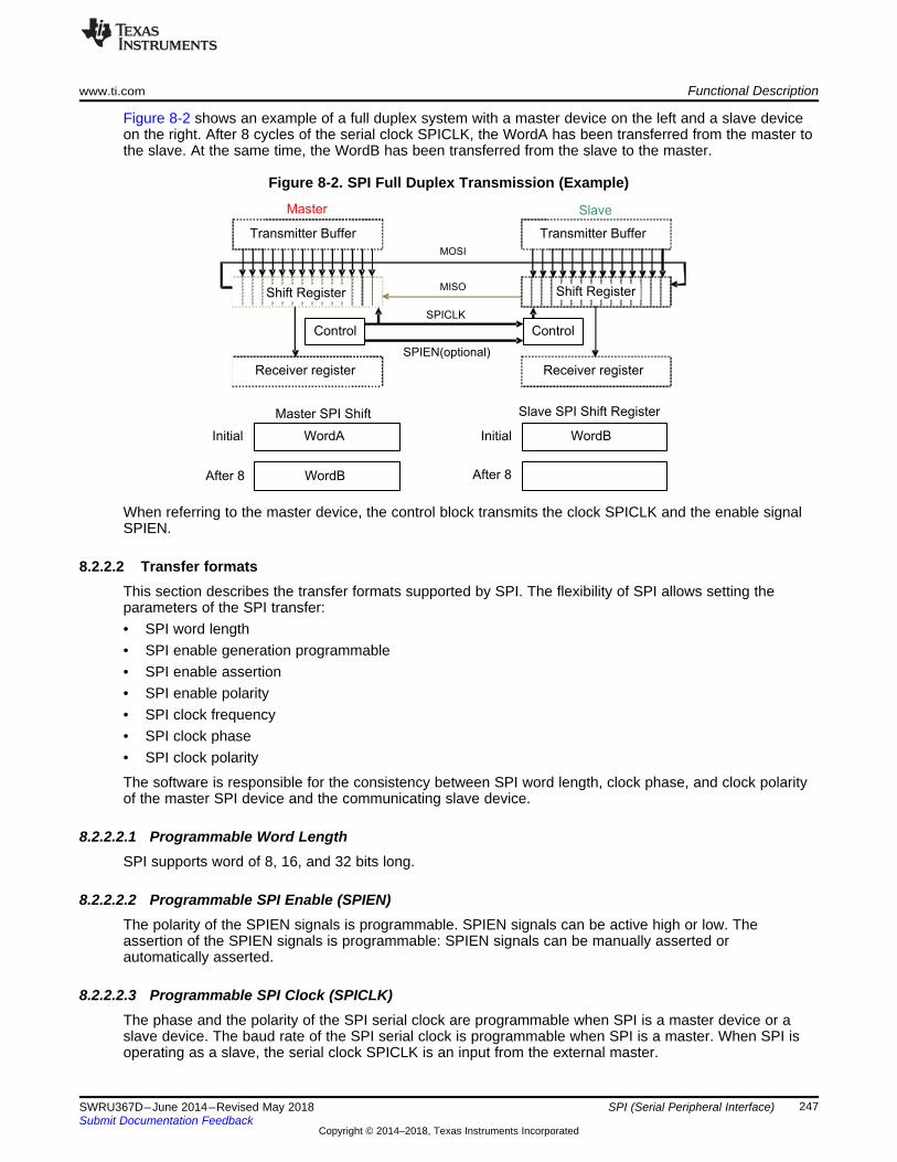
www.ti.com Functional Description
247SWRU367D–June 2014–Revised May 2018Submit Documentation Feedback
Copyright © 2014–2018, Texas Instruments Incorporated
SPI (Serial Peripheral Interface)
Figure 8-2 shows an example of a full duplex system with a master device on the left and a slave deviceon the right. After 8 cycles of the serial clock SPICLK, the WordA has been transferred from the master tothe slave. At the same time, the WordB has been transferred from the slave to the master.
Figure 8-2. SPI Full Duplex Transmission (Example)
When referring to the master device, the control block transmits the clock SPICLK and the enable signalSPIEN.
8.2.2.2 Transfer formatsThis section describes the transfer formats supported by SPI. The flexibility of SPI allows setting theparameters of the SPI transfer:• SPI word length• SPI enable generation programmable• SPI enable assertion• SPI enable polarity• SPI clock frequency• SPI clock phase• SPI clock polarity
The software is responsible for the consistency between SPI word length, clock phase, and clock polarityof the master SPI device and the communicating slave device.
8.2.2.2.1 Programmable Word LengthSPI supports word of 8, 16, and 32 bits long.
8.2.2.2.2 Programmable SPI Enable (SPIEN)The polarity of the SPIEN signals is programmable. SPIEN signals can be active high or low. Theassertion of the SPIEN signals is programmable: SPIEN signals can be manually asserted orautomatically asserted.
8.2.2.2.3 Programmable SPI Clock (SPICLK)The phase and the polarity of the SPI serial clock are programmable when SPI is a master device or aslave device. The baud rate of the SPI serial clock is programmable when SPI is a master. When SPI isoperating as a slave, the serial clock SPICLK is an input from the external master.
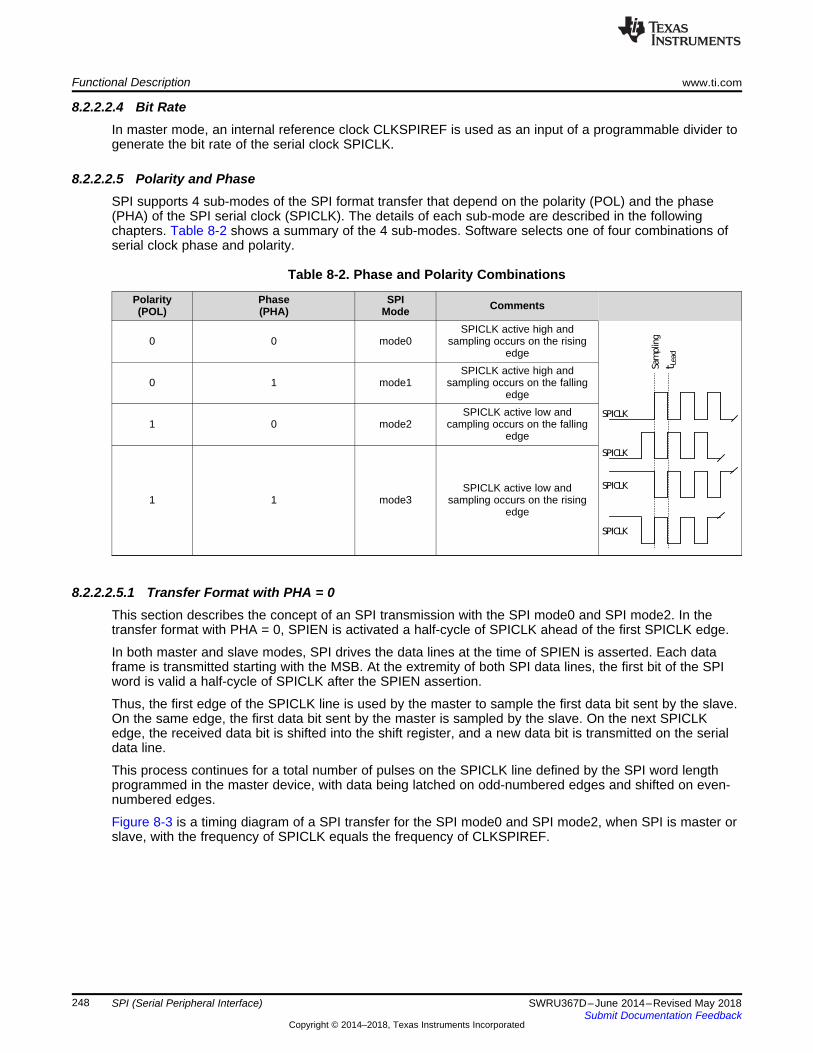
Functional Description www.ti.com
248 SWRU367D–June 2014–Revised May 2018Submit Documentation Feedback
Copyright © 2014–2018, Texas Instruments Incorporated
SPI (Serial Peripheral Interface)
8.2.2.2.4 Bit RateIn master mode, an internal reference clock CLKSPIREF is used as an input of a programmable divider togenerate the bit rate of the serial clock SPICLK.
8.2.2.2.5 Polarity and PhaseSPI supports 4 sub-modes of the SPI format transfer that depend on the polarity (POL) and the phase(PHA) of the SPI serial clock (SPICLK). The details of each sub-mode are described in the followingchapters. Table 8-2 shows a summary of the 4 sub-modes. Software selects one of four combinations ofserial clock phase and polarity.
Table 8-2. Phase and Polarity Combinations
Polarity(POL)
Phase(PHA)
SPIMode Comments
0 0 mode0SPICLK active high and
sampling occurs on the risingedge
0 1 mode1SPICLK active high and
sampling occurs on the fallingedge
1 0 mode2SPICLK active low and
campling occurs on the fallingedge
1 1 mode3SPICLK active low and
sampling occurs on the risingedge
8.2.2.2.5.1 Transfer Format with PHA = 0This section describes the concept of an SPI transmission with the SPI mode0 and SPI mode2. In thetransfer format with PHA = 0, SPIEN is activated a half-cycle of SPICLK ahead of the first SPICLK edge.
In both master and slave modes, SPI drives the data lines at the time of SPIEN is asserted. Each dataframe is transmitted starting with the MSB. At the extremity of both SPI data lines, the first bit of the SPIword is valid a half-cycle of SPICLK after the SPIEN assertion.
Thus, the first edge of the SPICLK line is used by the master to sample the first data bit sent by the slave.On the same edge, the first data bit sent by the master is sampled by the slave. On the next SPICLKedge, the received data bit is shifted into the shift register, and a new data bit is transmitted on the serialdata line.
This process continues for a total number of pulses on the SPICLK line defined by the SPI word lengthprogrammed in the master device, with data being latched on odd-numbered edges and shifted on even-numbered edges.
Figure 8-3 is a timing diagram of a SPI transfer for the SPI mode0 and SPI mode2, when SPI is master orslave, with the frequency of SPICLK equals the frequency of CLKSPIREF.
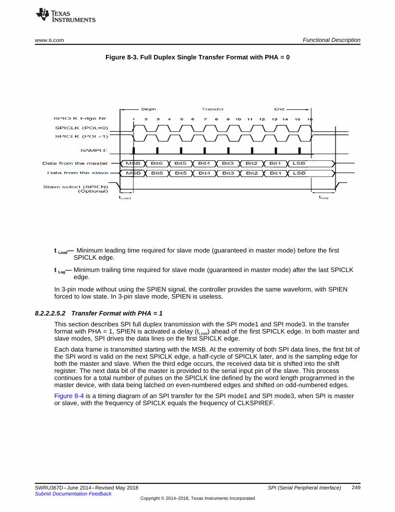
www.ti.com Functional Description
249SWRU367D–June 2014–Revised May 2018Submit Documentation Feedback
Copyright © 2014–2018, Texas Instruments Incorporated
SPI (Serial Peripheral Interface)
Figure 8-3. Full Duplex Single Transfer Format with PHA = 0
t Lead— Minimum leading time required for slave mode (guaranteed in master mode) before the firstSPICLK edge.
t Lag— Minimum trailing time required for slave mode (guaranteed in master mode) after the last SPICLKedge.
In 3-pin mode without using the SPIEN signal, the controller provides the same waveform, with SPIENforced to low state. In 3-pin slave mode, SPIEN is useless.
8.2.2.2.5.2 Transfer Format with PHA = 1This section describes SPI full duplex transmission with the SPI mode1 and SPI mode3. In the transferformat with PHA = 1, SPIEN is activated a delay (tLead) ahead of the first SPICLK edge. In both master andslave modes, SPI drives the data lines on the first SPICLK edge.
Each data frame is transmitted starting with the MSB. At the extremity of both SPI data lines, the first bit ofthe SPI word is valid on the next SPICLK edge, a half-cycle of SPICLK later, and is the sampling edge forboth the master and slave. When the third edge occurs, the received data bit is shifted into the shiftregister. The next data bit of the master is provided to the serial input pin of the slave. This processcontinues for a total number of pulses on the SPICLK line defined by the word length programmed in themaster device, with data being latched on even-numbered edges and shifted on odd-numbered edges.
Figure 8-4 is a timing diagram of an SPI transfer for the SPI mode1 and SPI mode3, when SPI is masteror slave, with the frequency of SPICLK equals the frequency of CLKSPIREF.
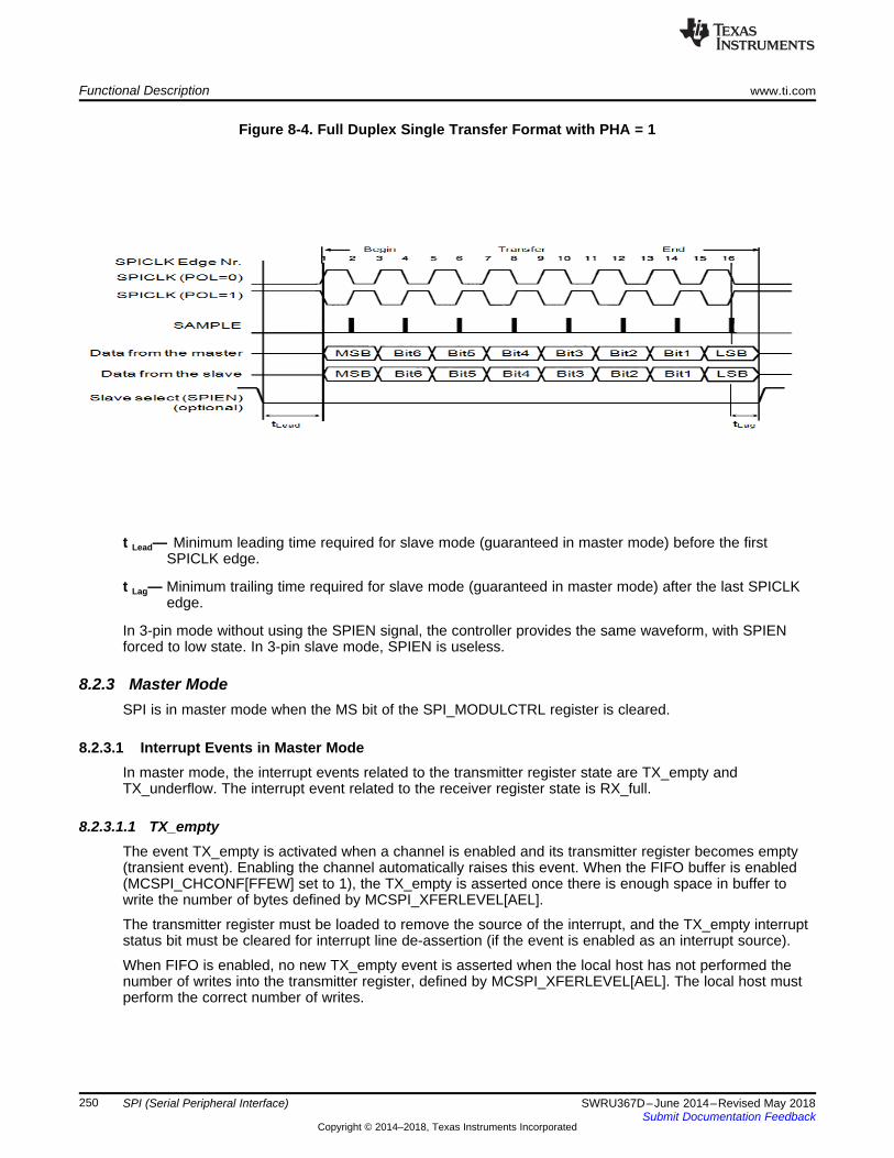
Functional Description www.ti.com
250 SWRU367D–June 2014–Revised May 2018Submit Documentation Feedback
Copyright © 2014–2018, Texas Instruments Incorporated
SPI (Serial Peripheral Interface)
Figure 8-4. Full Duplex Single Transfer Format with PHA = 1
t Lead— Minimum leading time required for slave mode (guaranteed in master mode) before the firstSPICLK edge.
t Lag— Minimum trailing time required for slave mode (guaranteed in master mode) after the last SPICLKedge.
In 3-pin mode without using the SPIEN signal, the controller provides the same waveform, with SPIENforced to low state. In 3-pin slave mode, SPIEN is useless.
8.2.3 Master ModeSPI is in master mode when the MS bit of the SPI_MODULCTRL register is cleared.
8.2.3.1 Interrupt Events in Master ModeIn master mode, the interrupt events related to the transmitter register state are TX_empty andTX_underflow. The interrupt event related to the receiver register state is RX_full.
8.2.3.1.1 TX_emptyThe event TX_empty is activated when a channel is enabled and its transmitter register becomes empty(transient event). Enabling the channel automatically raises this event. When the FIFO buffer is enabled(MCSPI_CHCONF[FFEW] set to 1), the TX_empty is asserted once there is enough space in buffer towrite the number of bytes defined by MCSPI_XFERLEVEL[AEL].
The transmitter register must be loaded to remove the source of the interrupt, and the TX_empty interruptstatus bit must be cleared for interrupt line de-assertion (if the event is enabled as an interrupt source).
When FIFO is enabled, no new TX_empty event is asserted when the local host has not performed thenumber of writes into the transmitter register, defined by MCSPI_XFERLEVEL[AEL]. The local host mustperform the correct number of writes.
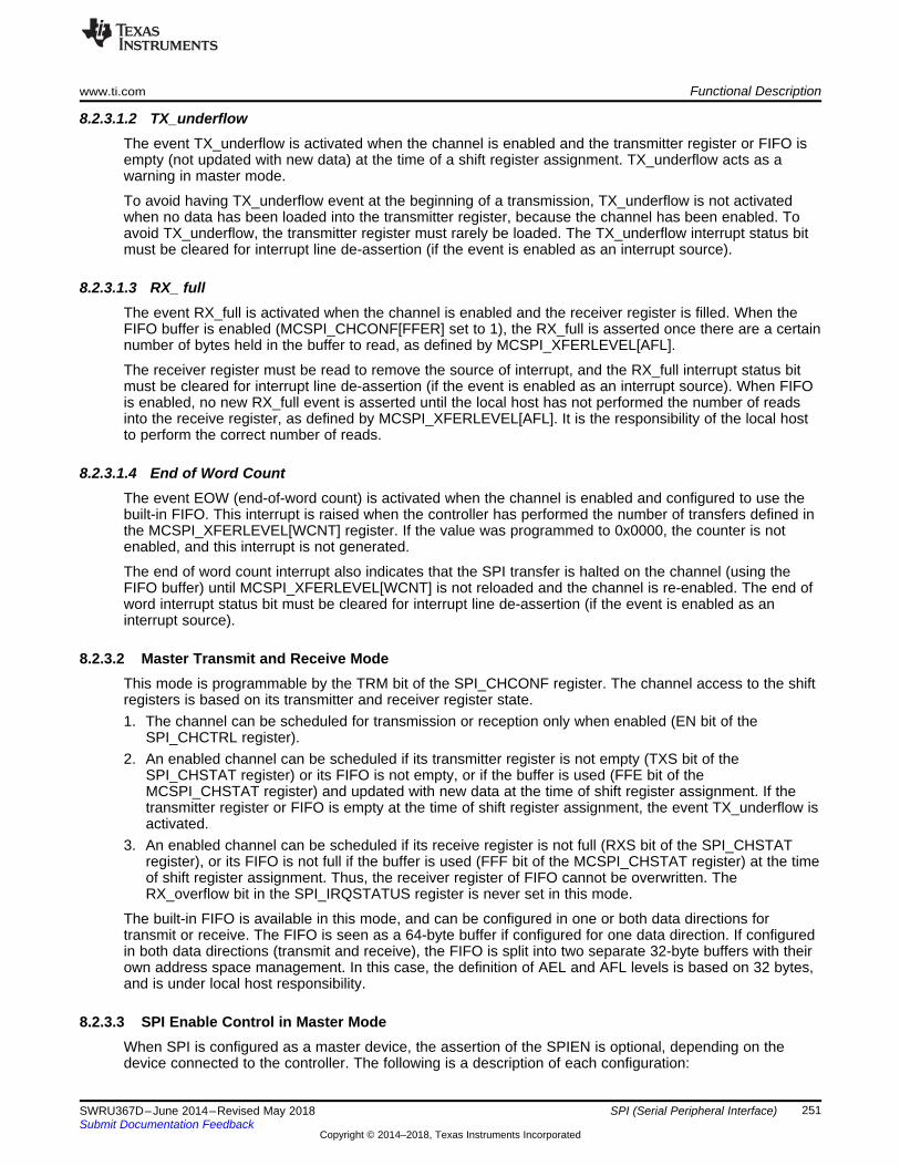
www.ti.com Functional Description
251SWRU367D–June 2014–Revised May 2018Submit Documentation Feedback
Copyright © 2014–2018, Texas Instruments Incorporated
SPI (Serial Peripheral Interface)
8.2.3.1.2 TX_underflowThe event TX_underflow is activated when the channel is enabled and the transmitter register or FIFO isempty (not updated with new data) at the time of a shift register assignment. TX_underflow acts as awarning in master mode.
To avoid having TX_underflow event at the beginning of a transmission, TX_underflow is not activatedwhen no data has been loaded into the transmitter register, because the channel has been enabled. Toavoid TX_underflow, the transmitter register must rarely be loaded. The TX_underflow interrupt status bitmust be cleared for interrupt line de-assertion (if the event is enabled as an interrupt source).
8.2.3.1.3 RX_ fullThe event RX_full is activated when the channel is enabled and the receiver register is filled. When theFIFO buffer is enabled (MCSPI_CHCONF[FFER] set to 1), the RX_full is asserted once there are a certainnumber of bytes held in the buffer to read, as defined by MCSPI_XFERLEVEL[AFL].
The receiver register must be read to remove the source of interrupt, and the RX_full interrupt status bitmust be cleared for interrupt line de-assertion (if the event is enabled as an interrupt source). When FIFOis enabled, no new RX_full event is asserted until the local host has not performed the number of readsinto the receive register, as defined by MCSPI_XFERLEVEL[AFL]. It is the responsibility of the local hostto perform the correct number of reads.
8.2.3.1.4 End of Word CountThe event EOW (end-of-word count) is activated when the channel is enabled and configured to use thebuilt-in FIFO. This interrupt is raised when the controller has performed the number of transfers defined inthe MCSPI_XFERLEVEL[WCNT] register. If the value was programmed to 0x0000, the counter is notenabled, and this interrupt is not generated.
The end of word count interrupt also indicates that the SPI transfer is halted on the channel (using theFIFO buffer) until MCSPI_XFERLEVEL[WCNT] is not reloaded and the channel is re-enabled. The end ofword interrupt status bit must be cleared for interrupt line de-assertion (if the event is enabled as aninterrupt source).
8.2.3.2 Master Transmit and Receive ModeThis mode is programmable by the TRM bit of the SPI_CHCONF register. The channel access to the shiftregisters is based on its transmitter and receiver register state.1. The channel can be scheduled for transmission or reception only when enabled (EN bit of the
SPI_CHCTRL register).2. An enabled channel can be scheduled if its transmitter register is not empty (TXS bit of the
SPI_CHSTAT register) or its FIFO is not empty, or if the buffer is used (FFE bit of theMCSPI_CHSTAT register) and updated with new data at the time of shift register assignment. If thetransmitter register or FIFO is empty at the time of shift register assignment, the event TX_underflow isactivated.
3. An enabled channel can be scheduled if its receive register is not full (RXS bit of the SPI_CHSTATregister), or its FIFO is not full if the buffer is used (FFF bit of the MCSPI_CHSTAT register) at the timeof shift register assignment. Thus, the receiver register of FIFO cannot be overwritten. TheRX_overflow bit in the SPI_IRQSTATUS register is never set in this mode.
The built-in FIFO is available in this mode, and can be configured in one or both data directions fortransmit or receive. The FIFO is seen as a 64-byte buffer if configured for one data direction. If configuredin both data directions (transmit and receive), the FIFO is split into two separate 32-byte buffers with theirown address space management. In this case, the definition of AEL and AFL levels is based on 32 bytes,and is under local host responsibility.
8.2.3.3 SPI Enable Control in Master ModeWhen SPI is configured as a master device, the assertion of the SPIEN is optional, depending on thedevice connected to the controller. The following is a description of each configuration:
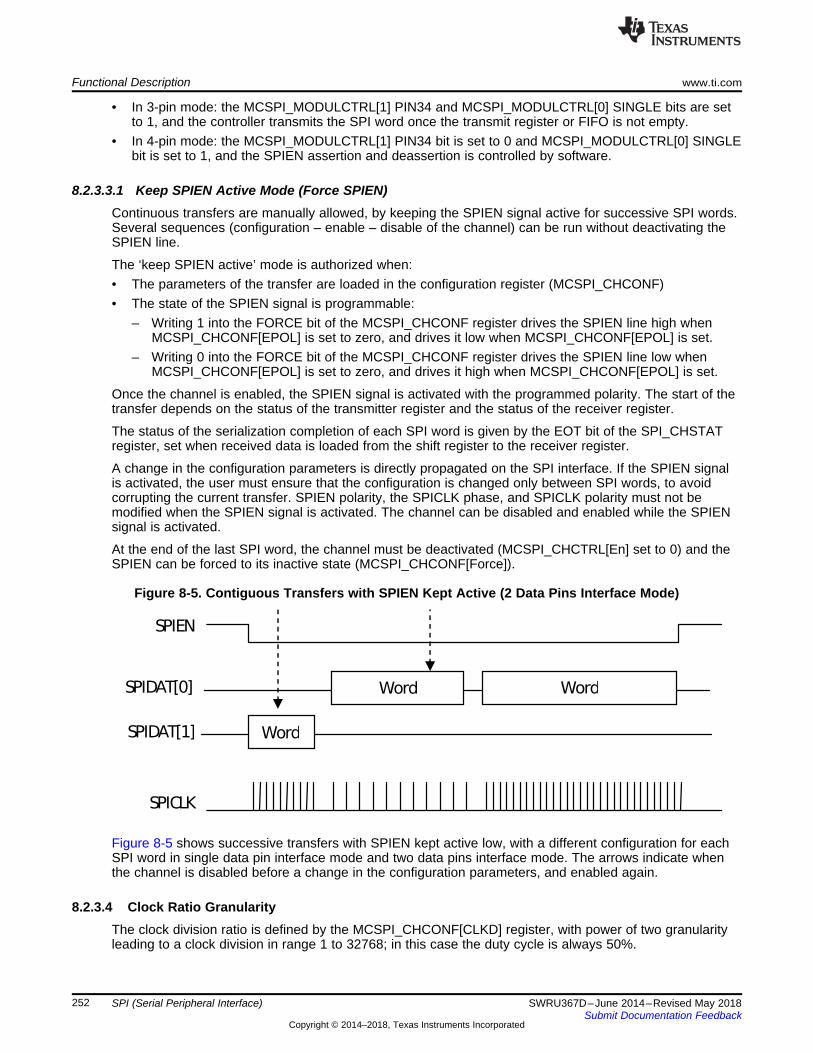
Functional Description www.ti.com
252 SWRU367D–June 2014–Revised May 2018Submit Documentation Feedback
Copyright © 2014–2018, Texas Instruments Incorporated
SPI (Serial Peripheral Interface)
• In 3-pin mode: the MCSPI_MODULCTRL[1] PIN34 and MCSPI_MODULCTRL[0] SINGLE bits are setto 1, and the controller transmits the SPI word once the transmit register or FIFO is not empty.
• In 4-pin mode: the MCSPI_MODULCTRL[1] PIN34 bit is set to 0 and MCSPI_MODULCTRL[0] SINGLEbit is set to 1, and the SPIEN assertion and deassertion is controlled by software.
8.2.3.3.1 Keep SPIEN Active Mode (Force SPIEN)Continuous transfers are manually allowed, by keeping the SPIEN signal active for successive SPI words.Several sequences (configuration – enable – disable of the channel) can be run without deactivating theSPIEN line.
The ‘keep SPIEN active’ mode is authorized when:• The parameters of the transfer are loaded in the configuration register (MCSPI_CHCONF)• The state of the SPIEN signal is programmable:
– Writing 1 into the FORCE bit of the MCSPI_CHCONF register drives the SPIEN line high whenMCSPI_CHCONF[EPOL] is set to zero, and drives it low when MCSPI_CHCONF[EPOL] is set.
– Writing 0 into the FORCE bit of the MCSPI_CHCONF register drives the SPIEN line low whenMCSPI_CHCONF[EPOL] is set to zero, and drives it high when MCSPI_CHCONF[EPOL] is set.
Once the channel is enabled, the SPIEN signal is activated with the programmed polarity. The start of thetransfer depends on the status of the transmitter register and the status of the receiver register.
The status of the serialization completion of each SPI word is given by the EOT bit of the SPI_CHSTATregister, set when received data is loaded from the shift register to the receiver register.
A change in the configuration parameters is directly propagated on the SPI interface. If the SPIEN signalis activated, the user must ensure that the configuration is changed only between SPI words, to avoidcorrupting the current transfer. SPIEN polarity, the SPICLK phase, and SPICLK polarity must not bemodified when the SPIEN signal is activated. The channel can be disabled and enabled while the SPIENsignal is activated.
At the end of the last SPI word, the channel must be deactivated (MCSPI_CHCTRL[En] set to 0) and theSPIEN can be forced to its inactive state (MCSPI_CHCONF[Force]).
Figure 8-5. Contiguous Transfers with SPIEN Kept Active (2 Data Pins Interface Mode)
Figure 8-5 shows successive transfers with SPIEN kept active low, with a different configuration for eachSPI word in single data pin interface mode and two data pins interface mode. The arrows indicate whenthe channel is disabled before a change in the configuration parameters, and enabled again.
8.2.3.4 Clock Ratio GranularityThe clock division ratio is defined by the MCSPI_CHCONF[CLKD] register, with power of two granularityleading to a clock division in range 1 to 32768; in this case the duty cycle is always 50%.

www.ti.com Functional Description
253SWRU367D–June 2014–Revised May 2018Submit Documentation Feedback
Copyright © 2014–2018, Texas Instruments Incorporated
SPI (Serial Peripheral Interface)
Table 8-3. Clock Ratio Granularity
Clock RatioF ratio
CLKSPIO High Time CLKSPIO Low Time
1 T high_ref T low_refEven ≥ 2 T_ref × (F ratio/2) T_ref × (F ratio/2)
Granularity examples with a clock source frequency of 48 Mhz:
Table 8-4. Granularity Examples
MCSPI_CHCONF
[CLKD]
F ratio
MCSPI_CHCONF
[PHA]
MCSPI_CHCONF
[POL]T high(ns)
T low(ns)
T period(ns) Duty Cycle F out
(Mhz)
0 1 X X 10.4 10.4 20.8 50-50 481 2 X X 20.8 20.8 41.6 50-50 242 4 X X 41.6 41.6 83.2 50-50 123 8 X X 83.2 83.2 166.4 50-50 6
8.2.3.4.1 FIFO Buffer ManagementThe SPI controller has a built-in 64-byte buffer to unload the DMA or interrupt handler and improve datathroughput. This buffer can be used by setting MCSPI_CHCONF[FFER] or MCSPI_CHCONF[FFEW] to 1.The buffer can be used in the modes defined below:• Master or slave mode• Every word length MCSPI_CHCONF[WL] are supported.
Two levels, AEL and AFL, located in the MCSPI_XFERLEVEL register, rule the buffer management. Thedriver must set these values as a multiple of SPI word length defined in MCSPI_CHCONF[WL]. Thenumber of bytes written in the FIFO depends on word length (see Table 8-5). The FIFO buffer pointers arereset when the channel is enabled, or when the FIFO configuration changes.
Table 8-5. SPI Word Length WL
SPI Word Length8 16 and 32
Number of bytes writtenin the FIFO 2 Bytes 4 Bytes
8.2.3.4.1.1 Split FIFOThe FIFO can be split into two parts when the module is configured in transmit/receive mode,MCSPI_CHCONF[TRM] set to 0, and MCSPI_CHCONF[FFER] and MCSPI_CHCONF[FFEW] asserted.Then system can access a 32-byte depth FIFO per direction.
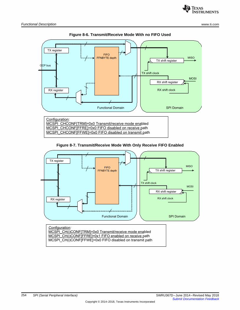
Functional Description www.ti.com
254 SWRU367D–June 2014–Revised May 2018Submit Documentation Feedback
Copyright © 2014–2018, Texas Instruments Incorporated
SPI (Serial Peripheral Interface)
Figure 8-6. Transmit/Receive Mode With no FIFO Used
Figure 8-7. Transmit/Receive Mode With Only Receive FIFO Enabled
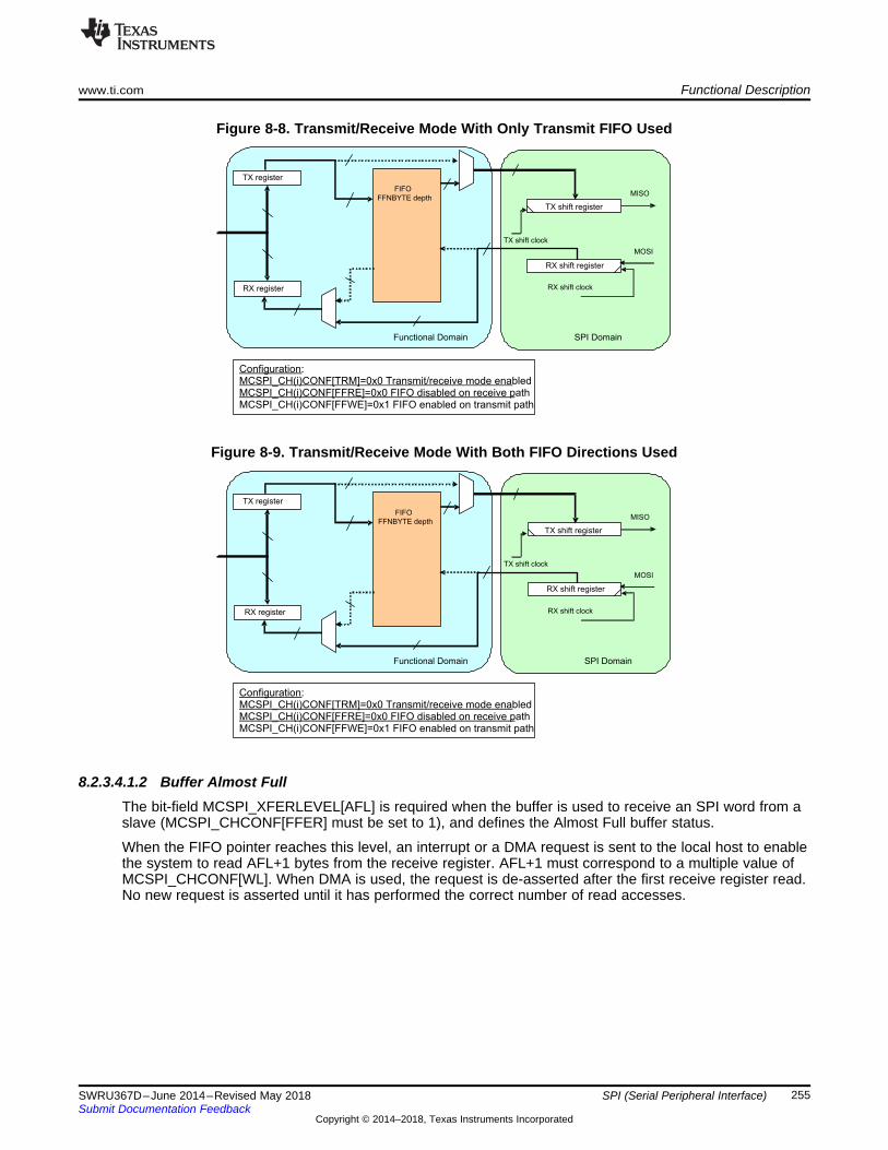
www.ti.com Functional Description
255SWRU367D–June 2014–Revised May 2018Submit Documentation Feedback
Copyright © 2014–2018, Texas Instruments Incorporated
SPI (Serial Peripheral Interface)
Figure 8-8. Transmit/Receive Mode With Only Transmit FIFO Used
Figure 8-9. Transmit/Receive Mode With Both FIFO Directions Used
8.2.3.4.1.2 Buffer Almost FullThe bit-field MCSPI_XFERLEVEL[AFL] is required when the buffer is used to receive an SPI word from aslave (MCSPI_CHCONF[FFER] must be set to 1), and defines the Almost Full buffer status.
When the FIFO pointer reaches this level, an interrupt or a DMA request is sent to the local host to enablethe system to read AFL+1 bytes from the receive register. AFL+1 must correspond to a multiple value ofMCSPI_CHCONF[WL]. When DMA is used, the request is de-asserted after the first receive register read.No new request is asserted until it has performed the correct number of read accesses.
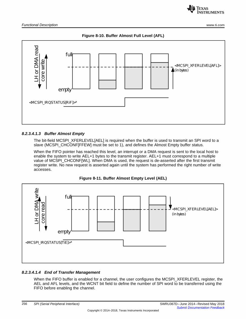
Functional Description www.ti.com
256 SWRU367D–June 2014–Revised May 2018Submit Documentation Feedback
Copyright © 2014–2018, Texas Instruments Incorporated
SPI (Serial Peripheral Interface)
Figure 8-10. Buffer Almost Full Level (AFL)
8.2.3.4.1.3 Buffer Almost EmptyThe bit-field MCSPI_XFERLEVEL[AEL] is required when the buffer is used to transmit an SPI word to aslave (MCSPI_CHCONF[FFEW] must be set to 1), and defines the Almost Empty buffer status.
When the FIFO pointer has reached this level, an interrupt or a DMA request is sent to the local host toenable the system to write AEL+1 bytes to the transmit register. AEL+1 must correspond to a multiplevalue of MCSPI_CHCONF[WL]. When DMA is used, the request is de-asserted after the first transmitregister write. No new request is asserted again until the system has performed the right number of writeaccesses.
Figure 8-11. Buffer Almost Empty Level (AEL)
8.2.3.4.1.4 End of Transfer ManagementWhen the FIFO buffer is enabled for a channel, the user configures the MCSPI_XFERLEVEL register, theAEL and AFL levels, and the WCNT bit field to define the number of SPI word to be transferred using theFIFO before enabling the channel.
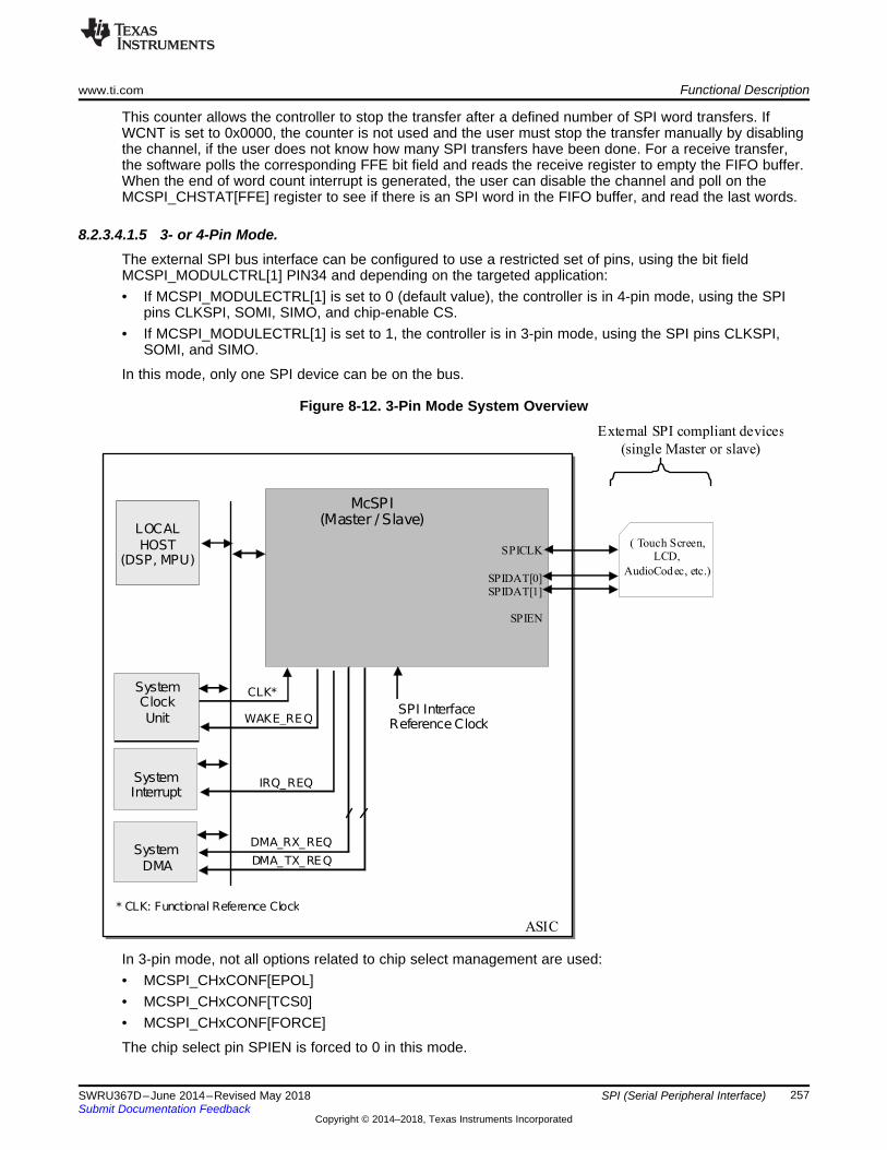
www.ti.com Functional Description
257SWRU367D–June 2014–Revised May 2018Submit Documentation Feedback
Copyright © 2014–2018, Texas Instruments Incorporated
SPI (Serial Peripheral Interface)
This counter allows the controller to stop the transfer after a defined number of SPI word transfers. IfWCNT is set to 0x0000, the counter is not used and the user must stop the transfer manually by disablingthe channel, if the user does not know how many SPI transfers have been done. For a receive transfer,the software polls the corresponding FFE bit field and reads the receive register to empty the FIFO buffer.When the end of word count interrupt is generated, the user can disable the channel and poll on theMCSPI_CHSTAT[FFE] register to see if there is an SPI word in the FIFO buffer, and read the last words.
8.2.3.4.1.5 3- or 4-Pin Mode.The external SPI bus interface can be configured to use a restricted set of pins, using the bit fieldMCSPI_MODULCTRL[1] PIN34 and depending on the targeted application:• If MCSPI_MODULECTRL[1] is set to 0 (default value), the controller is in 4-pin mode, using the SPI
pins CLKSPI, SOMI, SIMO, and chip-enable CS.• If MCSPI_MODULECTRL[1] is set to 1, the controller is in 3-pin mode, using the SPI pins CLKSPI,
SOMI, and SIMO.
In this mode, only one SPI device can be on the bus.
Figure 8-12. 3-Pin Mode System Overview
In 3-pin mode, not all options related to chip select management are used:• MCSPI_CHxCONF[EPOL]• MCSPI_CHxCONF[TCS0]• MCSPI_CHxCONF[FORCE]
The chip select pin SPIEN is forced to 0 in this mode.
Functional Description www.ti.com
258 SWRU367D–June 2014–Revised May 2018Submit Documentation Feedback
Copyright © 2014–2018, Texas Instruments Incorporated
SPI (Serial Peripheral Interface)
8.2.4 Slave ModeSPI is in slave mode when the MS bit of the SPI_MODULCTRL register is set. In slave mode, SPI shouldbe connected to only one external master device.
In slave mode, SPI initiates data transfer on the data lines (MISO/MOSI) when it receives an SPI clock(SPICLK) from the external SPI master device. The controller is able to work with or without a chip-selectSPIEN, depending on the MCSPI_MODULCTRL[1] PIN34 bit setting. It also support transfers without adead cycle between two successive words.
The following configurations are available for the slave channel:• A channel enable, programmable with the EN bit of the SPI_CHCTRL register. This channel should be
enabled before transmission and reception. Disabling the channel, outside data word transmission, isthe user's responsibility.
• A transmitter register, SPI_TX, on top of the common shift register. If the transmitter register is empty,the TXS status bit of the SPI_CHSTAT register is set. When SPI is selected by an external master(active signal on the SPIEN port), the transmitter register content of the channel is always loaded in theshift register, whether it has been updated or not. The transmitter register should be loaded before SPIis selected by a master.
• A receiver register, SPI_RX, on top of the common shift register. If the receiver register is full, the RXSstatus bit of the SPI_CHSTAT register is set.
• A communication configuration with the following parameters in the MCSPI_CHCONF register:– Transmit and receive modes, programmable with the TRM bit.– SPI word length, programmable with the WL bits.– SPIEN polarity, programmable with the EPOL bit.– SPICLK polarity, programmable with the POL bit.– SPICLK phase, programmable with the PHA bit.– Use a FIFO buffer or not, programmable with FFER and FFEW, depending on transfer mode TRM.– The SPICLK frequency of a transfer is controlled by the external SPI master.– Two DMA requests events, read and write, to synchronize read/write accesses of the DMA
controller with the activity of SPI. The DMA requests are enabled with the DMAR and DMAW bits ofthe MCSPI_CHCONF register.
8.2.4.1 Interrupts Events in Slave ModeThe interrupt events related to the transmitter register state are TX_empty and TX_underflow. Theinterrupt events related to the receiver register state are RX_full and RX_overflow.
8.2.4.1.1 TX_emptyThe TX_empty event activates when the channel is enabled and its transmitter register becomes empty.Enabling the channel automatically raises this event. When the FIFO buffer is enabled(MCSPI_CHCONF[FFEW] set to 1), the TX_empty is asserted once there is enough space in buffer towrite a number of bytes defined by MCSPI_XFERLEVEL[AEL].
The transmitter register must be loaded to remove the source of the interrupt, and the TX_empty interruptstatus bit must be cleared for the interrupt line de-assertion (if the event is enabled as the interruptsource).
When FIFO is enabled, no new TX_empty event is asserted if the local host has not performed thenumber of writes into the transmitter register defined by MCSPI_XFERLEVEL[AEL]. The local host mustperform the correct number of writes.
8.2.4.1.2 TX_underflowThe TX_underflow event activates when the channel is enabled and the transmitter register or FIFO (ifbuffer is enabled) is empty (not updated with new data), and when an external master device starts a datatransfer with SPI (transmit and receive).
www.ti.com Functional Description
259SWRU367D–June 2014–Revised May 2018Submit Documentation Feedback
Copyright © 2014–2018, Texas Instruments Incorporated
SPI (Serial Peripheral Interface)
When FIFO is enabled, the data emitted while the underflow event is raised is not the last data written inthe FIFO. The TX_underflow indicates an error (data loss) in slave mode.
To avoid having a TX_underflow event at the beginning of a transmission, the event TX_underflow is notactivated when no data has been loaded into the transmitter register, because the channel has beenenabled. The TX_underflow interrupt status bit must be cleared for an interrupt line de-assertion (if eventis enabled as the interrupt source).
8.2.4.1.3 RX_ fullThe RX_full event activates when the channel is enabled and the receiver is filled (transient event). Whenthe FIFO buffer is enabled (MCSPI_CHCONF[FFER] set to 1), the RX_full is asserted once there is anumber of bytes held in the buffer to read defined by MCSPI_XFERLEVEL[AFL].
The receiver register must be read to remove the source of the interrupt, and the RX_full interrupt statusbit must be cleared for an interrupt line de-assertion (if the event is enabled as an interrupt source).
When FIFO is enabled, no new RX_full event is asserted if the local host has not performed the number ofreads into the receive register defined by MCSPI_XFERLEVEL[AFL]. The local host must perform thecorrect number of reads.
8.2.4.1.4 RX_overflowThe RX_overflow event activates when the channel is enabled and the receiver register or FIFO (if thebuffer is enabled) is full at the time of a new SPI word reception. The receiver register is alwaysoverwritten with the new SPI word. If FIFO is enabled and the data within the FIFO is overwritten, it mustbe corrupted.
The RX_overflow event should not appear in slave mode using the FIFO. The RX_overflow indicates anerror (data loss) in slave mode. The RX_overflow interrupt status bit must be cleared for an interrupt linede-assertion (if the event is enabled as an interrupt source).
8.2.4.1.5 End-of-Word CountThe EOW (end-of-word count) event activates when the channel is enabled and configured to use thebuilt-in FIFO. This interrupt is raised when the controller performs the number of transfers defined in theMCSPI_XFERLEVEL[WCNT] register. If the value is programmed to 0x0000, the counter is not enabledand this interrupt is not generated.
The end-of-word count interrupt also indicates that the SPI transfer is stopped on the channel using theFIFO buffer, once MCSPI_XFERLEVEL[WCNT] is not reloaded and the channel re-enabled. The end-of-word interrupt status bit must be cleared for the interrupt line de-assertion (if the event is enabled as aninterrupt source).
8.2.4.2 Slave Transmit and Receive ModeThe slave transmit and receive mode is programmable (TRM bits set to 00 in the register SPI_CHCONF).After the channel is enabled, transmission and reception proceed with interrupt and DMA request events.
In slave transmit and receive mode, the transmitter register should be loaded before SPI is selected by anexternal SPI master device. The transmitter register or FIFO (if the use of a buffer is enabled) content isalways loaded in the shift register, whether updated or not. The TX_underflow event activates, and doesnot prevent transmission.
Upon completion of SPI word transfer (EOT bit of the SPI_CHSTAT register is set), the received data istransferred to the channel receive register. This bit is meaningless when using the buffer for this channel.
The built-in FIFO is available in this mode and can be configured in one data direction, either transmit orreceive, to ensure that the FIFO is seen as a unique 64-byte buffer. The FIFO can also be configured inboth data transmit and receive directions, to ensure the FIFO is split into two separate 32-byte buffers withindividual address space management. In this last case, the definition of the AEL and AFL levels is basedon 64 bytes, and is the responsibility of the local host.
Functional Description www.ti.com
260 SWRU367D–June 2014–Revised May 2018Submit Documentation Feedback
Copyright © 2014–2018, Texas Instruments Incorporated
SPI (Serial Peripheral Interface)
8.2.5 InterruptsAccording to the transmitter register state and the receiver register state, the channel can issue interruptevents if enabled. Each interrupt event has a status bit in the SPI_IRQSTATUS register that indicatesservice is required, and an interrupt enable bit in the SPI_IRQENABLE register that enables the status togenerate hardware interrupt requests. When an interrupt occurs and a mask is then applied on it(IRQENABLE), the interrupt line is not asserted again, even if the interrupt source has not been serviced.
SPI supports interrupt-driven operation and polling.
8.2.5.1 Interrupt-Driven OperationAlternatively, an interrupt enable bit in the SPI_IRQENABLE register can be set to enable each of theevents to generate interrupt requests when the corresponding event occurs. Status bits are automaticallyset by hardware logic conditions.
When an event occurs (the single interrupt line is asserted), the local host must:• Read the SPI_IRQSTATUS register to identify which event occurred.• Interrupt handling:
– Read the receiver register that corresponds to the event, to remove the source of an RX_full event,or
– Write into the transmitter register that corresponds to the event, to remove the source of aTX_empty event.
– No action is needed to remove the source of the events TX_underflow and RX_overflow.• Write a 1 into the corresponding bit of the SPI_IRQSTATUS register to clear the interrupt status and
release the interrupt line.
The interrupt status bit should always be reset after channel enabling and before events are enabled asan interrupt source.
8.2.5.2 PollingWhen the interrupt capability of an event is disabled in the SPI_IRQENABLE register, the interrupt line isnot asserted and:• The status bits in the SPI_IRQSTATUS register is polled by software to detect when the corresponding
event occurs.• Once the expected event occurs, the local host must read the receiver register that corresponds to the
event to remove the source of an RX_full event, or write into the transmitter register that correspondsto the event to remove the source of a TX_empty event. No action is needed to remove the source ofthe events TX_underflow and RX_overflow.
• Writing a 1 into the corresponding bit of the SPI_IRQSTATUS register clears the interrupt status anddoes not affect the interrupt line state.
8.2.6 DMA RequestsSPI can be interfaced with a DMA controller. At the system level, the advantage is to discharge the localhost of the data transfers. According to FIFO level (if using a buffer for the channel), the channel can issueDMA requests if enabled. The DMA requests must be disabled to get TX and RX interrupts. There are twoDMA request lines for the channel.
8.2.6.1 FIFO Buffer EnabledThe DMA read request line asserts when the channel is enabled and a number of bytes defined inSPI_XFERLEVEL[AFL] bit field is held in the FIFO buffer for the receive register of the channel. A DMAread request can be individually masked with the DMAR bit of the SPI_CHCONF register. The DMA readrequest line is de-asserted on the first SPI word read completion of the receive register of the channel. Nonew DMA request is asserted if the user has not performed the correct number of read accesses, asdefined by SPI_XFERLEVEL[AFL].
www.ti.com Functional Description
261SWRU367D–June 2014–Revised May 2018Submit Documentation Feedback
Copyright © 2014–2018, Texas Instruments Incorporated
SPI (Serial Peripheral Interface)
The DMA write request line asserts when the channel is enabled and the number of bytes held in theFIFO buffer is below the level defined by the SPI_XFERLEVEL[AEL] bit field. A DMA write request can beindividually masked with the DMAW bit of the SPI_CHCONF register. The DMA write request line assertswhen the channel is enabled and the number of bytes held in the FIFO buffer is below the level defined bythe SPI_XFERLEVEL[AEL] bit field.
8.2.7 ResetThe module can be reset by software through the SoftReset bit of the SPI_SYSCONFIG register. TheSPI_SYSCONFIG register is not sensitive to software reset. The SoftReset control bit is active high. Thebit is automatically reset to 0 by the hardware.
A global ResetDone status bit is provided in the SPI_SYSCONFIG status register. The global ResetDonestatus bit can be monitored by the software to check if the module is ready to use following a reset.
8.3 Initialization and ConfigurationThis section describes a GSPI module initialization and configuration example for each of the two basicmodes supported to transmit and receive at 100000 KHz.
8.3.1 Basic Initializationa. Enable the SPI module clock by invoking the following API:
PRCMPeripheralClkEnable(PRCM_GSPI,PRCM_RUN_MODE_CLK)
b. Set the pinmux to bring out the SPI signals to the chip boundary at desired location:
PinTypeSPI(<pin_no>, <mode>).
c. Soft reset the module:
SPIReset(GSPI_BASE)
8.3.2 Master Mode Operation Without Interrupt (Polling)a. Configure the SPI with following parameters:
• Mode: 4-pin/master• Sub mode: 0• Bit Rate: 100000 Hz• Chip Select: Software-controlled/active high• Word Length: 8 bitsSPIConfigSetExpClk(GSPI_BASE,PRCMPeripheralClockGet(PRCM_GSPI),100000, SPI_MODE_MASTER,SPI_SUB_MODE_0, (SPI_SW_CTRL_CS | SPI_4PIN_MODE|SPI_TURBO_OFF |SPI_CS_ACTIVEHIGH |SPI_WL_8))
b. Enable SPI channel for communication:
SPIEnable(GSPI_BASE)
c. Enable chip select:
SPICSEnable(GSPI_BASE)
d. Write new data into TX FIFO to transmit over the interface:
SPIDataPut(GSPI_BASE,<UserData>);
e. Read received data from the RX FIFO:
SPIDataGet(GSPI_BASE,&<ulDummy>)
f. Disable chip select:
SPICSDisable(GSPI_BASE)
Initialization and Configuration www.ti.com
262 SWRU367D–June 2014–Revised May 2018Submit Documentation Feedback
Copyright © 2014–2018, Texas Instruments Incorporated
SPI (Serial Peripheral Interface)
8.3.3 Slave Mode Operation With Interrupta. Set the interrupt vector table base and enable master interrupt for NVIC:
IntVTableBaseSet( <address_of_vector_table> )IntMasterEnable()
b. Configure the SPI with following parameters:• Mode: 4-pin/slave• Word Length: 8 bitsSPIConfigSetExpClk(GSPI_BASE,PRCMPeripheralClockGet(PRCM_GSPI),SPI_IF_BIT_RATE, SPI_MODE_SLAVE, SPI_SUB_MODE_0,(SPI_HW_CTRL_CS |SPI_4PIN_MODE |SPI_TURBO_OFF |SPI_CS_ACTIVEHIGH |SPI_WL_8))
c. Register the interrupt handler:
SPIIntRegister(GSPI_BASE, <SlaveIntHandler> )
d. Enable the transmit empty and receive full interrupts:
SPIIntEnable(GSPI_BASE,SPI_INT_RX_FULL|SPI_INT_TX_EMPTY)
e. Enable SPI channel for communication:
SPIEnable(GSPI_BASE)
8.3.4 Generic Interrupt Handler Implementationvoid SlaveIntHandler()
unsigned long ulDummy;unsigned long ulStatus;
// Read the interrupt statusulStatus = SPIIntStatus(GSPI_BASE,true);
// Acknowledge the interruptsSPIIntClear(GSPI_BASE,SPI_INT_RX_FULL|SPI_INT_TX_EMPTY);
// If TX empty, write a new data into SPI registerif(ulStatus & SPI_INT_TX_EMPTY)
SPIDataPut(GSPI_BASE,<user_data>)
// if RX is full, readout the data from SPIif(ulStatus & SPI_INT_RX_FULL)
SPIDataGetNonBlocking(GSPI_BASE,&ulDummy);
8.4 Access to Data RegistersThis section describes the supported data accesses (read or write) to and from the data receiver registersSPI_RX and data transmitter registers SPI_TX.
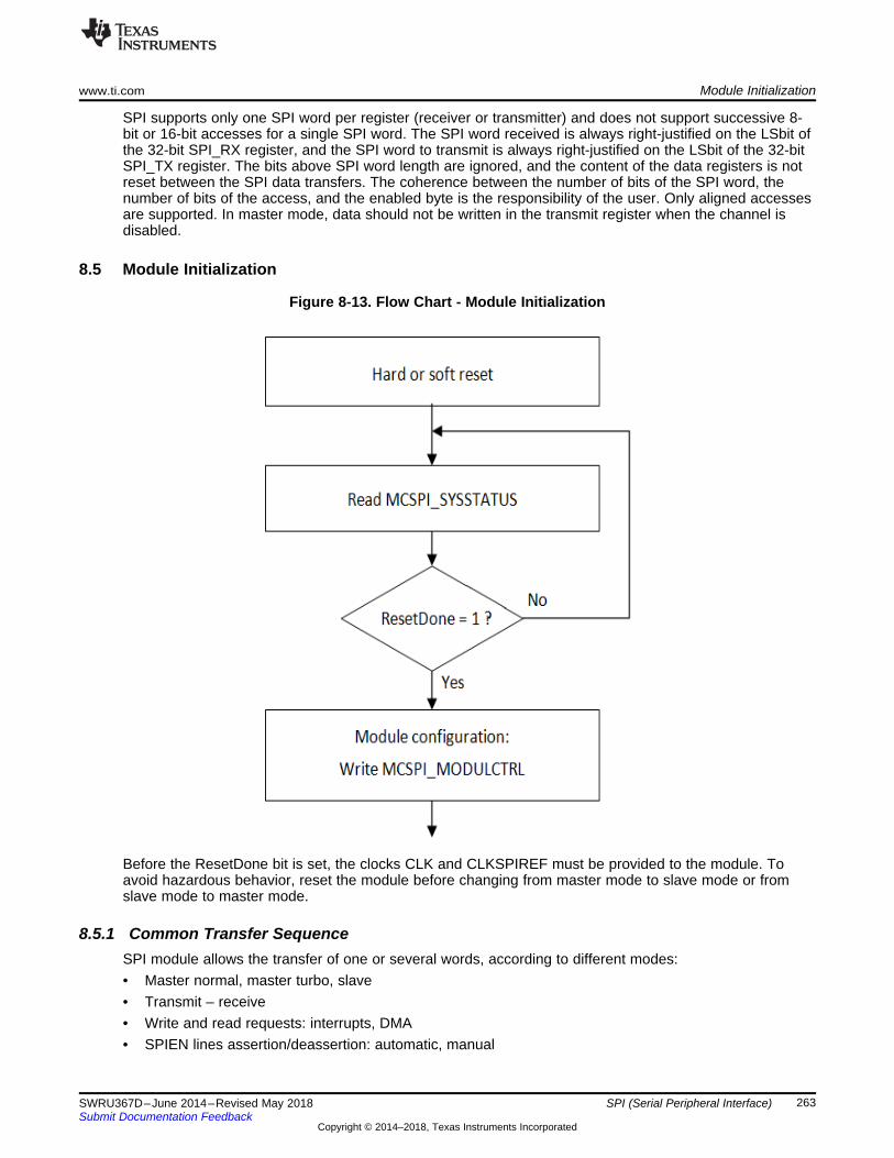
www.ti.com Module Initialization
263SWRU367D–June 2014–Revised May 2018Submit Documentation Feedback
Copyright © 2014–2018, Texas Instruments Incorporated
SPI (Serial Peripheral Interface)
SPI supports only one SPI word per register (receiver or transmitter) and does not support successive 8-bit or 16-bit accesses for a single SPI word. The SPI word received is always right-justified on the LSbit ofthe 32-bit SPI_RX register, and the SPI word to transmit is always right-justified on the LSbit of the 32-bitSPI_TX register. The bits above SPI word length are ignored, and the content of the data registers is notreset between the SPI data transfers. The coherence between the number of bits of the SPI word, thenumber of bits of the access, and the enabled byte is the responsibility of the user. Only aligned accessesare supported. In master mode, data should not be written in the transmit register when the channel isdisabled.
8.5 Module Initialization
Figure 8-13. Flow Chart - Module Initialization
Before the ResetDone bit is set, the clocks CLK and CLKSPIREF must be provided to the module. Toavoid hazardous behavior, reset the module before changing from master mode to slave mode or fromslave mode to master mode.
8.5.1 Common Transfer SequenceSPI module allows the transfer of one or several words, according to different modes:• Master normal, master turbo, slave• Transmit – receive• Write and read requests: interrupts, DMA• SPIEN lines assertion/deassertion: automatic, manual
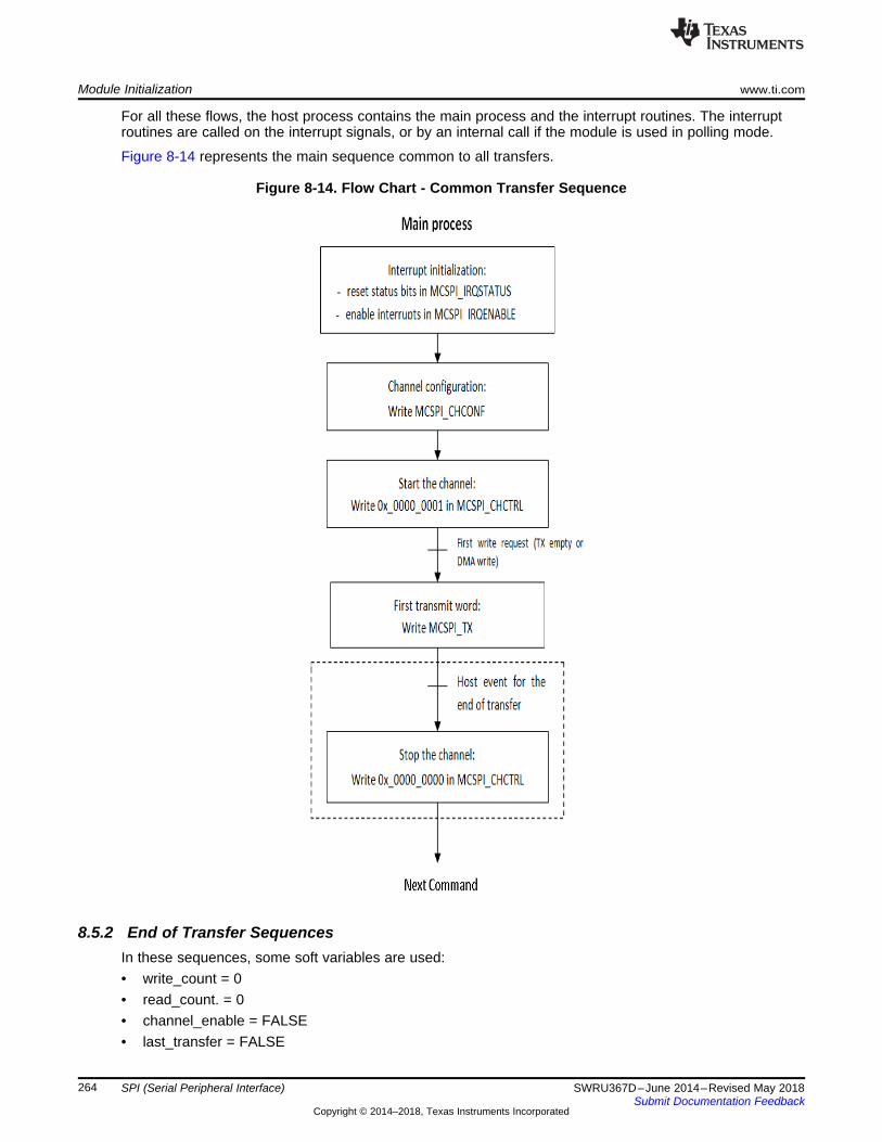
Module Initialization www.ti.com
264 SWRU367D–June 2014–Revised May 2018Submit Documentation Feedback
Copyright © 2014–2018, Texas Instruments Incorporated
SPI (Serial Peripheral Interface)
For all these flows, the host process contains the main process and the interrupt routines. The interruptroutines are called on the interrupt signals, or by an internal call if the module is used in polling mode.
Figure 8-14 represents the main sequence common to all transfers.
Figure 8-14. Flow Chart - Common Transfer Sequence
8.5.2 End of Transfer SequencesIn these sequences, some soft variables are used:• write_count = 0• read_count. = 0• channel_enable = FALSE• last_transfer = FALSE
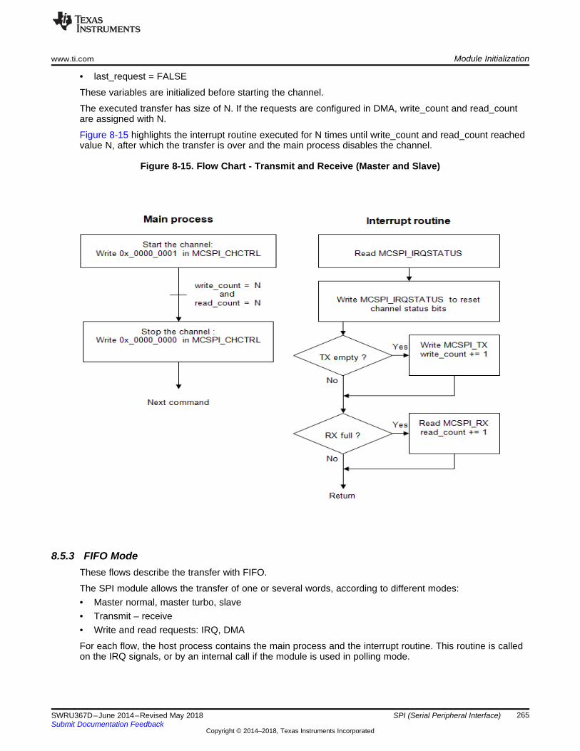
www.ti.com Module Initialization
265SWRU367D–June 2014–Revised May 2018Submit Documentation Feedback
Copyright © 2014–2018, Texas Instruments Incorporated
SPI (Serial Peripheral Interface)
• last_request = FALSE
These variables are initialized before starting the channel.
The executed transfer has size of N. If the requests are configured in DMA, write_count and read_countare assigned with N.
Figure 8-15 highlights the interrupt routine executed for N times until write_count and read_count reachedvalue N, after which the transfer is over and the main process disables the channel.
Figure 8-15. Flow Chart - Transmit and Receive (Master and Slave)
8.5.3 FIFO ModeThese flows describe the transfer with FIFO.
The SPI module allows the transfer of one or several words, according to different modes:• Master normal, master turbo, slave• Transmit – receive• Write and read requests: IRQ, DMA
For each flow, the host process contains the main process and the interrupt routine. This routine is calledon the IRQ signals, or by an internal call if the module is used in polling mode.
Module Initialization www.ti.com
266 SWRU367D–June 2014–Revised May 2018Submit Documentation Feedback
Copyright © 2014–2018, Texas Instruments Incorporated
SPI (Serial Peripheral Interface)
8.5.3.1 Common Transfer SequenceIn transmit and receive mode, the FIFO can be enabled for write or read request only. The SPI modulestarts the transfer only when the first write request is released, by writing the SPI_TX register. SeeFigure 8-16.
This first write request is managed by the IRQ routine or DMA handler.
The sequence varies according to whether word count is used or not (SPI_XFERLEVEL : WCNT ≠ 0 ornot). The AEL or AFL values can be different, but they must be a multiple of the word size in the FIFO: 1,2, or 4 bytes, according to word length.
In these sequences, the transfer to execute has a size of N words. In these sequences, the numbers ofword written or read for each write or read FIFO request are:• write_request_size• read_request_size
If they are not submultiples of N, the last request sizes are:• last_write_request_size ( < write_request_size )• last_read_request_size. ( < read_request_size)
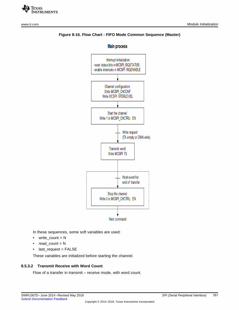
www.ti.com Module Initialization
267SWRU367D–June 2014–Revised May 2018Submit Documentation Feedback
Copyright © 2014–2018, Texas Instruments Incorporated
SPI (Serial Peripheral Interface)
Figure 8-16. Flow Chart - FIFO Mode Common Sequence (Master)
In these sequences, some soft variables are used:• write_count = N• read_count = N• last_request = FALSE
These variables are initialized before starting the channel.
8.5.3.2 Transmit Receive with Word CountFlow of a transfer in transmit – receive mode, with word count.
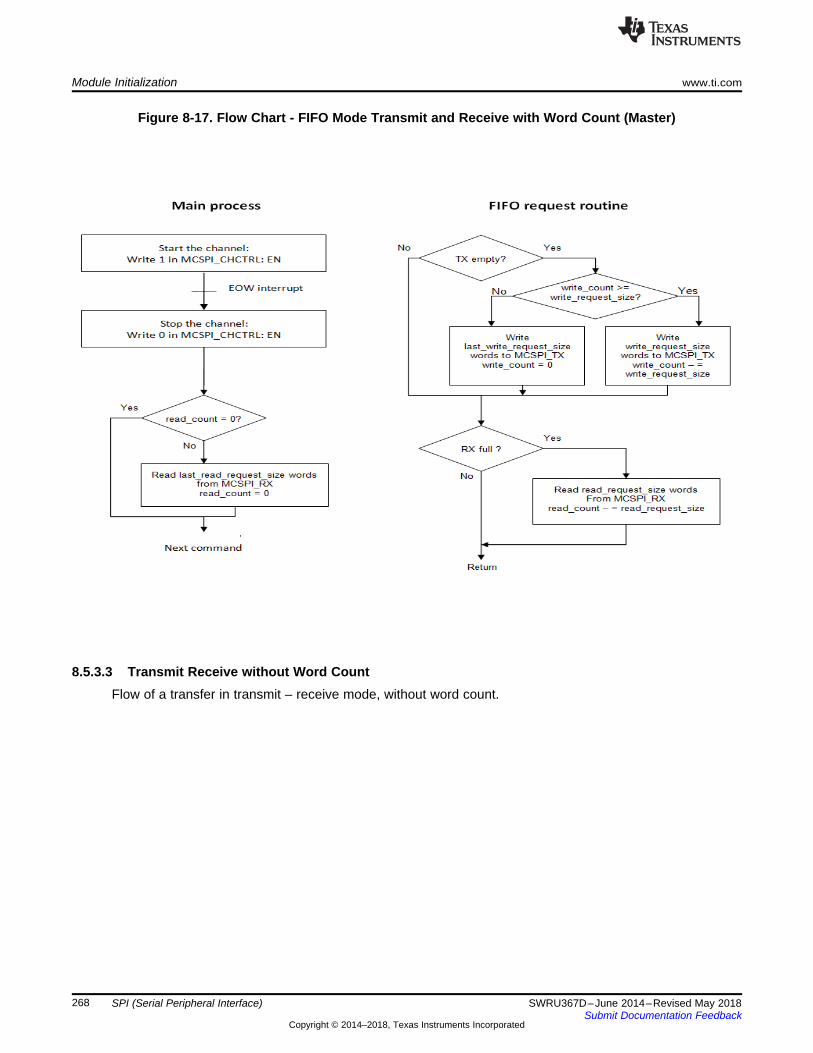
Module Initialization www.ti.com
268 SWRU367D–June 2014–Revised May 2018Submit Documentation Feedback
Copyright © 2014–2018, Texas Instruments Incorporated
SPI (Serial Peripheral Interface)
Figure 8-17. Flow Chart - FIFO Mode Transmit and Receive with Word Count (Master)
8.5.3.3 Transmit Receive without Word CountFlow of a transfer in transmit – receive mode, without word count.
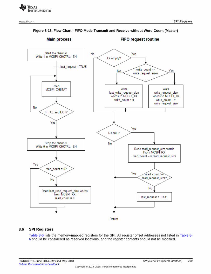
www.ti.com SPI Registers
269SWRU367D–June 2014–Revised May 2018Submit Documentation Feedback
Copyright © 2014–2018, Texas Instruments Incorporated
SPI (Serial Peripheral Interface)
Figure 8-18. Flow Chart - FIFO Mode Transmit and Receive without Word Count (Master)
8.6 SPI RegistersTable 8-6 lists the memory-mapped registers for the SPI. All register offset addresses not listed in Table 8-6 should be considered as reserved locations, and the register contents should not be modified.
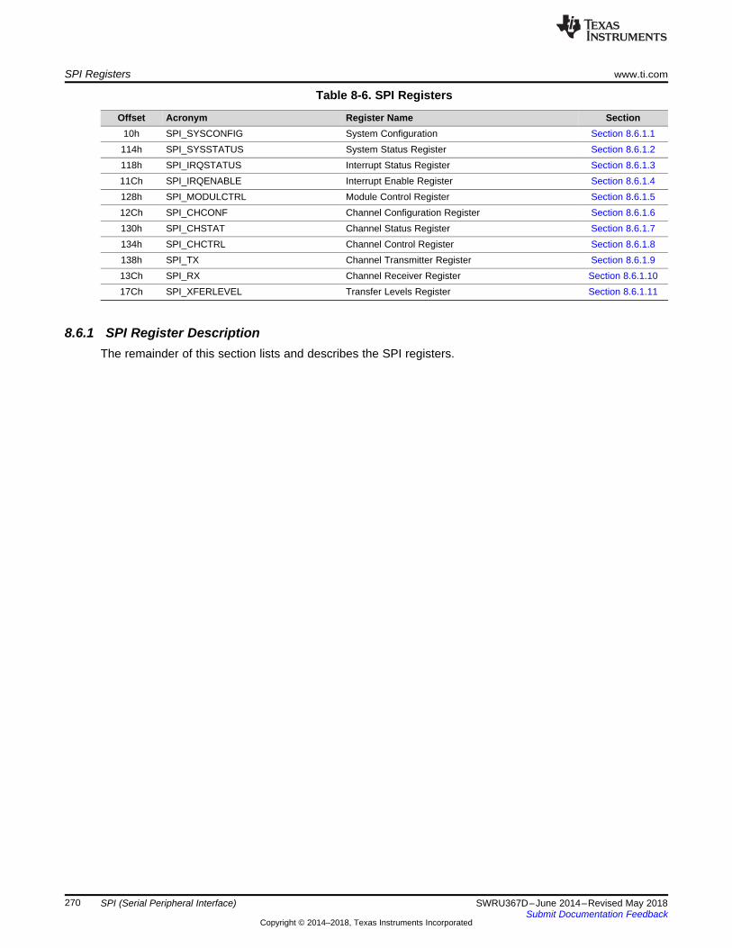
SPI Registers www.ti.com
270 SWRU367D–June 2014–Revised May 2018Submit Documentation Feedback
Copyright © 2014–2018, Texas Instruments Incorporated
SPI (Serial Peripheral Interface)
Table 8-6. SPI Registers
Offset Acronym Register Name Section10h SPI_SYSCONFIG System Configuration Section 8.6.1.1114h SPI_SYSSTATUS System Status Register Section 8.6.1.2118h SPI_IRQSTATUS Interrupt Status Register Section 8.6.1.311Ch SPI_IRQENABLE Interrupt Enable Register Section 8.6.1.4128h SPI_MODULCTRL Module Control Register Section 8.6.1.512Ch SPI_CHCONF Channel Configuration Register Section 8.6.1.6130h SPI_CHSTAT Channel Status Register Section 8.6.1.7134h SPI_CHCTRL Channel Control Register Section 8.6.1.8138h SPI_TX Channel Transmitter Register Section 8.6.1.913Ch SPI_RX Channel Receiver Register Section 8.6.1.1017Ch SPI_XFERLEVEL Transfer Levels Register Section 8.6.1.11
8.6.1 SPI Register DescriptionThe remainder of this section lists and describes the SPI registers.
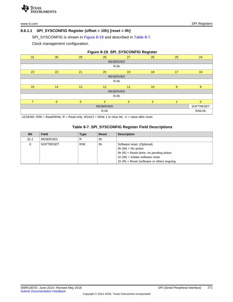
www.ti.com SPI Registers
271SWRU367D–June 2014–Revised May 2018Submit Documentation Feedback
Copyright © 2014–2018, Texas Instruments Incorporated
SPI (Serial Peripheral Interface)
8.6.1.1 SPI_SYSCONFIG Register (offset = 10h) [reset = 0h]SPI_SYSCONFIG is shown in Figure 8-19 and described in Table 8-7.
Clock management configuration.
Figure 8-19. SPI_SYSCONFIG Register31 30 29 28 27 26 25 24
RESERVEDR-0h
23 22 21 20 19 18 17 16RESERVED
R-0h
15 14 13 12 11 10 9 8RESERVED
R-0h
7 6 5 4 3 2 1 0RESERVED SOFTRESET
R-0h R/W-0h
LEGEND: R/W = Read/Write; R = Read only; W1toCl = Write 1 to clear bit; -n = value after reset
Table 8-7. SPI_SYSCONFIG Register Field Descriptions
Bit Field Type Reset Description31-1 RESERVED R 0h
0 SOFTRESET R/W 0h Software reset. (Optional)0h (W) = No action0h (R) = Reset done, no pending action1h (W) = Initiate software reset1h (R) = Reset (software or other) ongoing
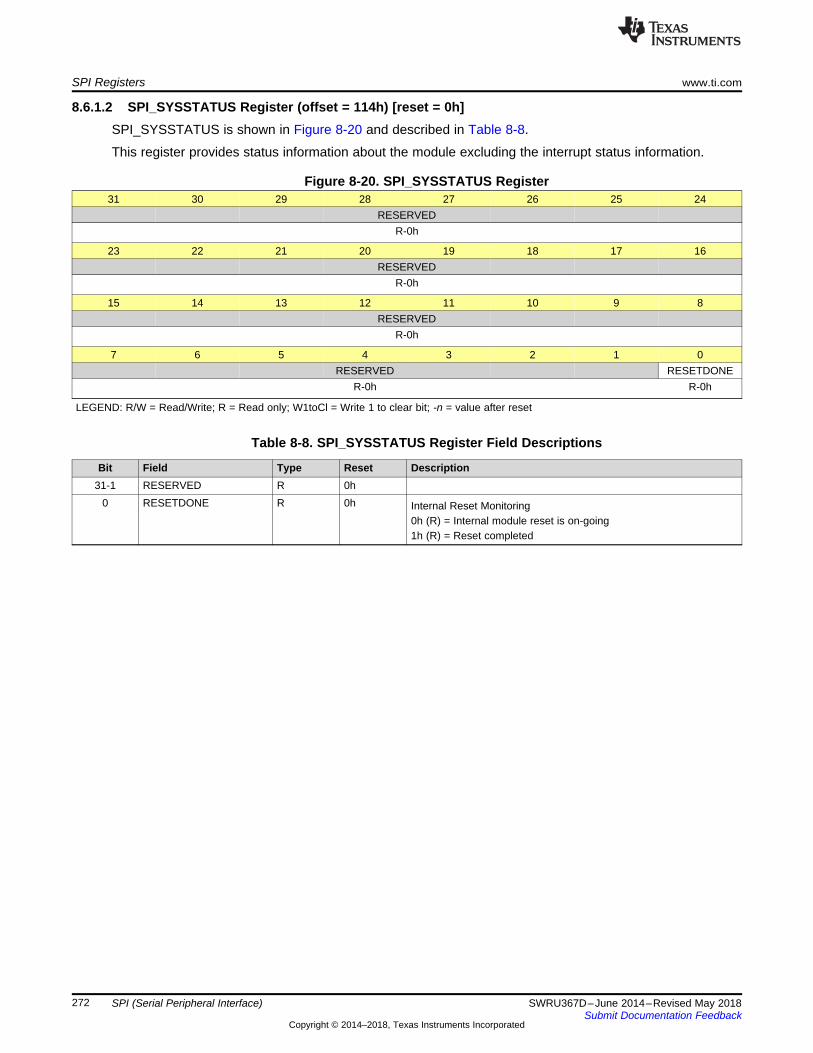
SPI Registers www.ti.com
272 SWRU367D–June 2014–Revised May 2018Submit Documentation Feedback
Copyright © 2014–2018, Texas Instruments Incorporated
SPI (Serial Peripheral Interface)
8.6.1.2 SPI_SYSSTATUS Register (offset = 114h) [reset = 0h]SPI_SYSSTATUS is shown in Figure 8-20 and described in Table 8-8.
This register provides status information about the module excluding the interrupt status information.
Figure 8-20. SPI_SYSSTATUS Register31 30 29 28 27 26 25 24
RESERVEDR-0h
23 22 21 20 19 18 17 16RESERVED
R-0h
15 14 13 12 11 10 9 8RESERVED
R-0h
7 6 5 4 3 2 1 0RESERVED RESETDONE
R-0h R-0h
LEGEND: R/W = Read/Write; R = Read only; W1toCl = Write 1 to clear bit; -n = value after reset
Table 8-8. SPI_SYSSTATUS Register Field Descriptions
Bit Field Type Reset Description31-1 RESERVED R 0h
0 RESETDONE R 0h Internal Reset Monitoring0h (R) = Internal module reset is on-going1h (R) = Reset completed
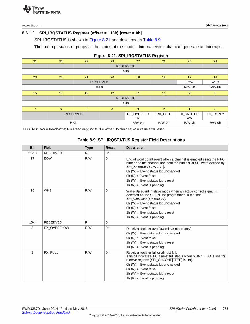
www.ti.com SPI Registers
273SWRU367D–June 2014–Revised May 2018Submit Documentation Feedback
Copyright © 2014–2018, Texas Instruments Incorporated
SPI (Serial Peripheral Interface)
8.6.1.3 SPI_IRQSTATUS Register (offset = 118h) [reset = 0h]SPI_IRQSTATUS is shown in Figure 8-21 and described in Table 8-9.
The interrupt status regroups all the status of the module internal events that can generate an interrupt.
Figure 8-21. SPI_IRQSTATUS Register31 30 29 28 27 26 25 24
RESERVEDR-0h
23 22 21 20 19 18 17 16RESERVED EOW WKS
R-0h R/W-0h R/W-0h
15 14 13 12 11 10 9 8RESERVED
R-0h
7 6 5 4 3 2 1 0RESERVED RX_OVERFLO
WRX_FULL TX_UNDERFL
OWTX_EMPTY
R-0h R/W-0h R/W-0h R/W-0h R/W-0h
LEGEND: R/W = Read/Write; R = Read only; W1toCl = Write 1 to clear bit; -n = value after reset
Table 8-9. SPI_IRQSTATUS Register Field Descriptions
Bit Field Type Reset Description31-18 RESERVED R 0h
17 EOW R/W 0h End of word count event when a channel is enabled using the FIFObuffer and the channel had sent the number of SPI word defined bySPI_XFERLEVEL[WCNT].0h (W) = Event status bit unchanged0h (R) = Event false1h (W) = Event status bit is reset1h (R) = Event is pending
16 WKS R/W 0h Wake Up event in slave mode when an active control signal isdetected on the SPIEN line programmed in the fieldSPI_CHCONF[SPIENSLV].0h (W) = Event status bit unchanged0h (R) = Event false1h (W) = Event status bit is reset1h (R) = Event is pending
15-4 RESERVED R 0h3 RX_OVERFLOW R/W 0h Receiver register overflow (slave mode only).
0h (W) = Event status bit unchanged0h (R) = Event false1h (W) = Event status bit is reset1h (R) = Event is pending
2 RX_FULL R/W 0h Receiver register full or almost full.This bit indicate FIFO almost full status when built-in FIFO is use forreceive register (SPI_CHCONF[FFER] is set).0h (W) = Event status bit unchanged0h (R) = Event false1h (W) = Event status bit is reset1h (R) = Event is pending

SPI Registers www.ti.com
274 SWRU367D–June 2014–Revised May 2018Submit Documentation Feedback
Copyright © 2014–2018, Texas Instruments Incorporated
SPI (Serial Peripheral Interface)
Table 8-9. SPI_IRQSTATUS Register Field Descriptions (continued)Bit Field Type Reset Description1 TX_UNDERFLOW R/W 0h Transmitter register underflow.
0h (W) = Event status bit unchanged0h (R) = Event false1h (W) = Event status bit is reset1h (R) = Event is pending
0 TX_EMPTY R/W 0h Transmitter register empty or almost empty.This bit indicate FIFO almost full status when built-in FIFO is use fortransmit register (SPI_CHCONF[FFEW] is set).0h (W) = Event status bit unchanged0h (R) = Event false1h (W) = Event status bit is reset1h (R) = Event is pending
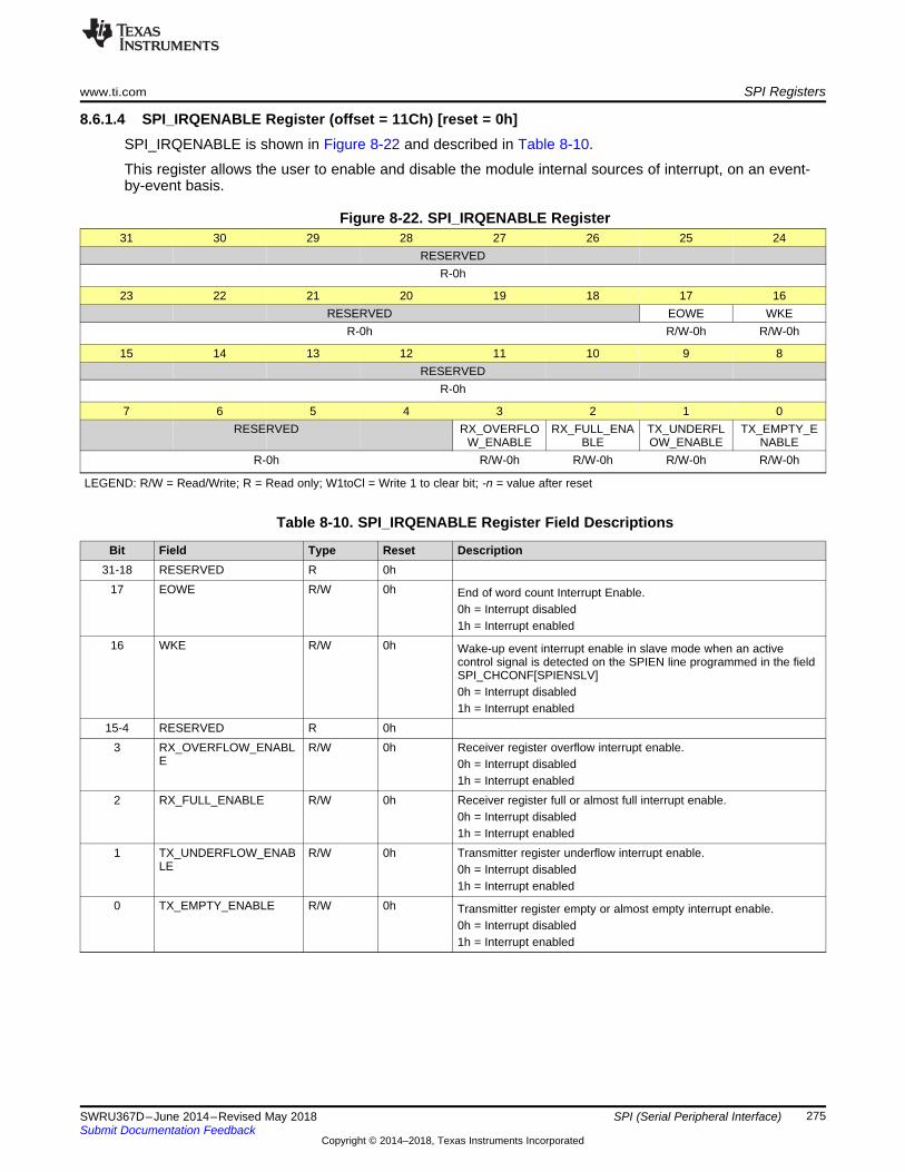
www.ti.com SPI Registers
275SWRU367D–June 2014–Revised May 2018Submit Documentation Feedback
Copyright © 2014–2018, Texas Instruments Incorporated
SPI (Serial Peripheral Interface)
8.6.1.4 SPI_IRQENABLE Register (offset = 11Ch) [reset = 0h]SPI_IRQENABLE is shown in Figure 8-22 and described in Table 8-10.
This register allows the user to enable and disable the module internal sources of interrupt, on an event-by-event basis.
Figure 8-22. SPI_IRQENABLE Register31 30 29 28 27 26 25 24
RESERVEDR-0h
23 22 21 20 19 18 17 16RESERVED EOWE WKE
R-0h R/W-0h R/W-0h
15 14 13 12 11 10 9 8RESERVED
R-0h
7 6 5 4 3 2 1 0RESERVED RX_OVERFLO
W_ENABLERX_FULL_ENA
BLETX_UNDERFLOW_ENABLE
TX_EMPTY_ENABLE
R-0h R/W-0h R/W-0h R/W-0h R/W-0h
LEGEND: R/W = Read/Write; R = Read only; W1toCl = Write 1 to clear bit; -n = value after reset
Table 8-10. SPI_IRQENABLE Register Field Descriptions
Bit Field Type Reset Description31-18 RESERVED R 0h
17 EOWE R/W 0h End of word count Interrupt Enable.0h = Interrupt disabled1h = Interrupt enabled
16 WKE R/W 0h Wake-up event interrupt enable in slave mode when an activecontrol signal is detected on the SPIEN line programmed in the fieldSPI_CHCONF[SPIENSLV]0h = Interrupt disabled1h = Interrupt enabled
15-4 RESERVED R 0h3 RX_OVERFLOW_ENABL
ER/W 0h Receiver register overflow interrupt enable.
0h = Interrupt disabled1h = Interrupt enabled
2 RX_FULL_ENABLE R/W 0h Receiver register full or almost full interrupt enable.0h = Interrupt disabled1h = Interrupt enabled
1 TX_UNDERFLOW_ENABLE
R/W 0h Transmitter register underflow interrupt enable.0h = Interrupt disabled1h = Interrupt enabled
0 TX_EMPTY_ENABLE R/W 0h Transmitter register empty or almost empty interrupt enable.0h = Interrupt disabled1h = Interrupt enabled
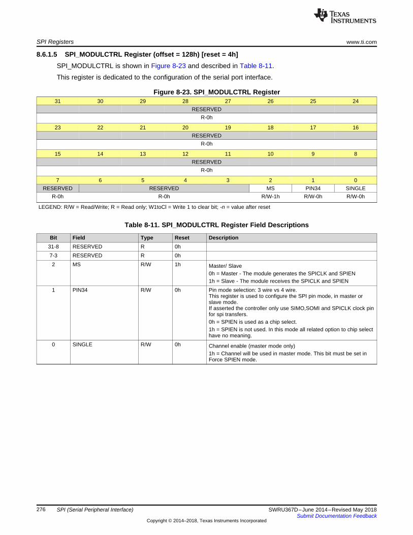
SPI Registers www.ti.com
276 SWRU367D–June 2014–Revised May 2018Submit Documentation Feedback
Copyright © 2014–2018, Texas Instruments Incorporated
SPI (Serial Peripheral Interface)
8.6.1.5 SPI_MODULCTRL Register (offset = 128h) [reset = 4h]SPI_MODULCTRL is shown in Figure 8-23 and described in Table 8-11.
This register is dedicated to the configuration of the serial port interface.
Figure 8-23. SPI_MODULCTRL Register31 30 29 28 27 26 25 24
RESERVEDR-0h
23 22 21 20 19 18 17 16RESERVED
R-0h
15 14 13 12 11 10 9 8RESERVED
R-0h
7 6 5 4 3 2 1 0RESERVED RESERVED MS PIN34 SINGLE
R-0h R-0h R/W-1h R/W-0h R/W-0h
LEGEND: R/W = Read/Write; R = Read only; W1toCl = Write 1 to clear bit; -n = value after reset
Table 8-11. SPI_MODULCTRL Register Field Descriptions
Bit Field Type Reset Description31-8 RESERVED R 0h7-3 RESERVED R 0h2 MS R/W 1h Master/ Slave
0h = Master - The module generates the SPICLK and SPIEN1h = Slave - The module receives the SPICLK and SPIEN
1 PIN34 R/W 0h Pin mode selection: 3 wire vs 4 wire.This register is used to configure the SPI pin mode, in master orslave mode.If asserted the controller only use SIMO,SOMI and SPICLK clock pinfor spi transfers.0h = SPIEN is used as a chip select.1h = SPIEN is not used. In this mode all related option to chip selecthave no meaning.
0 SINGLE R/W 0h Channel enable (master mode only)1h = Channel will be used in master mode. This bit must be set inForce SPIEN mode.
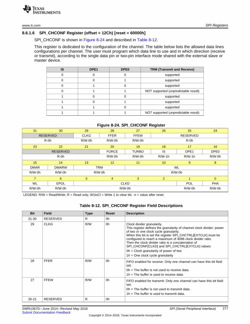
www.ti.com SPI Registers
277SWRU367D–June 2014–Revised May 2018Submit Documentation Feedback
Copyright © 2014–2018, Texas Instruments Incorporated
SPI (Serial Peripheral Interface)
8.6.1.6 SPI_CHCONF Register (offset = 12Ch) [reset = 60000h]SPI_CHCONF is shown in Figure 8-24 and described in Table 8-12.
This register is dedicated to the configuration of the channel. The table below lists the allowed data linesconfigurations per channel. The user must program which data line to use and in which direction (receiveor transmit), according to the single data pin or two-pin interface mode shared with the external slave ormaster device.
IS DPE1 DPE0 TRM (Transmit and Receive)0 0 0 supported0 0 1 supported0 1 0 supported0 1 1 NOT supported (unpredictable result)1 0 0 supported1 0 1 supported1 1 0 supported1 1 1 NOT supported (unpredictable result)
Figure 8-24. SPI_CHCONF Register31 30 29 28 27 26 25 24
RESERVED CLKG FFER FFEW RESERVEDR-0h R/W-0h R/W-0h R/W-0h R-0h
23 22 21 20 19 18 17 16RESERVED FORCE TURBO IS DPE1 DPE0
R-0h R/W-0h R/W-0h R/W-1h R/W-1h R/W-0h
15 14 13 12 11 10 9 8DMAR DMARW TRM WLR/W-0h R/W-0h R/W-0h R/W-0h
7 6 5 4 3 2 1 0WL EPOL CLKD POL PHA
R/W-0h R/W-0h R/W-0h R/W-0h R/W-0h
LEGEND: R/W = Read/Write; R = Read only; W1toCl = Write 1 to clear bit; -n = value after reset
Table 8-12. SPI_CHCONF Register Field Descriptions
Bit Field Type Reset Description31-30 RESERVED R 0h
29 CLKG R/W 0h Clock divider granularity.This register defines the granularity of channel clock divider: powerof two or one clock cycle granularity.When this bit is set the register SPI_CHCTRL[EXTCLK] must beconfigured to reach a maximum of 4096 clock divider ratio.Then the clock divider ratio is a concatenation ofSPI_CHCONF[CLKD] and SPI_CHCTRL[EXTCLK] values0h = Clock granularity of power of two1h = One clock cycle granularity
28 FFER R/W 0h FIFO enabled for receive: Only one channel can have this bit fieldset.0h = The buffer is not used to receive data.1h = The buffer is used to receive data.
27 FFEW R/W 0h FIFO enabled for transmit: Only one channel can have this bit fieldset.0h = The buffer is not used to transmit data.1h = The buffer is used to transmit data.
26-21 RESERVED R 0h
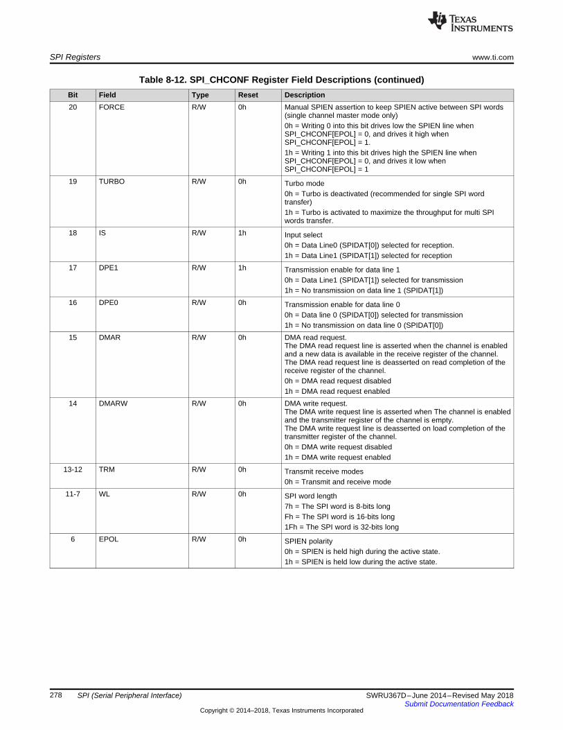
SPI Registers www.ti.com
278 SWRU367D–June 2014–Revised May 2018Submit Documentation Feedback
Copyright © 2014–2018, Texas Instruments Incorporated
SPI (Serial Peripheral Interface)
Table 8-12. SPI_CHCONF Register Field Descriptions (continued)Bit Field Type Reset Description20 FORCE R/W 0h Manual SPIEN assertion to keep SPIEN active between SPI words
(single channel master mode only)0h = Writing 0 into this bit drives low the SPIEN line whenSPI_CHCONF[EPOL] = 0, and drives it high whenSPI_CHCONF[EPOL] = 1.1h = Writing 1 into this bit drives high the SPIEN line whenSPI_CHCONF[EPOL] = 0, and drives it low whenSPI_CHCONF[EPOL] = 1
19 TURBO R/W 0h Turbo mode0h = Turbo is deactivated (recommended for single SPI wordtransfer)1h = Turbo is activated to maximize the throughput for multi SPIwords transfer.
18 IS R/W 1h Input select0h = Data Line0 (SPIDAT[0]) selected for reception.1h = Data Line1 (SPIDAT[1]) selected for reception
17 DPE1 R/W 1h Transmission enable for data line 10h = Data Line1 (SPIDAT[1]) selected for transmission1h = No transmission on data line 1 (SPIDAT[1])
16 DPE0 R/W 0h Transmission enable for data line 00h = Data line 0 (SPIDAT[0]) selected for transmission1h = No transmission on data line 0 (SPIDAT[0])
15 DMAR R/W 0h DMA read request.The DMA read request line is asserted when the channel is enabledand a new data is available in the receive register of the channel.The DMA read request line is deasserted on read completion of thereceive register of the channel.0h = DMA read request disabled1h = DMA read request enabled
14 DMARW R/W 0h DMA write request.The DMA write request line is asserted when The channel is enabledand the transmitter register of the channel is empty.The DMA write request line is deasserted on load completion of thetransmitter register of the channel.0h = DMA write request disabled1h = DMA write request enabled
13-12 TRM R/W 0h Transmit receive modes0h = Transmit and receive mode
11-7 WL R/W 0h SPI word length7h = The SPI word is 8-bits longFh = The SPI word is 16-bits long1Fh = The SPI word is 32-bits long
6 EPOL R/W 0h SPIEN polarity0h = SPIEN is held high during the active state.1h = SPIEN is held low during the active state.
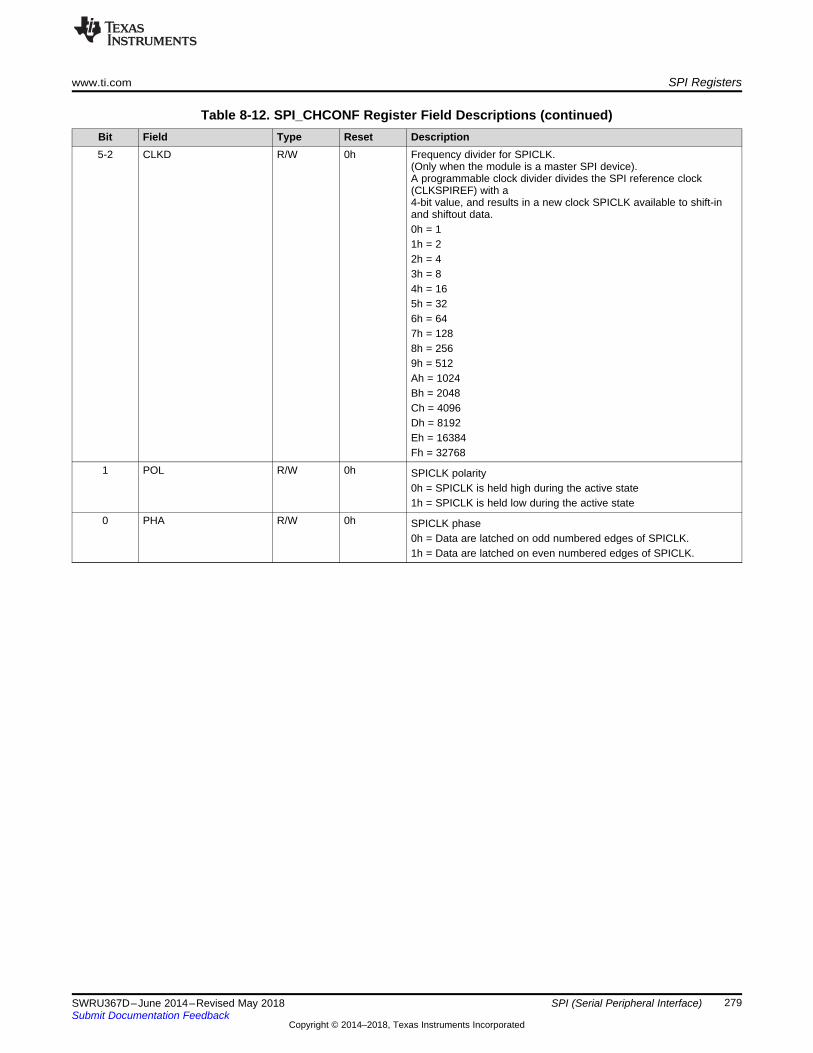
www.ti.com SPI Registers
279SWRU367D–June 2014–Revised May 2018Submit Documentation Feedback
Copyright © 2014–2018, Texas Instruments Incorporated
SPI (Serial Peripheral Interface)
Table 8-12. SPI_CHCONF Register Field Descriptions (continued)Bit Field Type Reset Description5-2 CLKD R/W 0h Frequency divider for SPICLK.
(Only when the module is a master SPI device).A programmable clock divider divides the SPI reference clock(CLKSPIREF) with a4-bit value, and results in a new clock SPICLK available to shift-inand shiftout data.0h = 11h = 22h = 43h = 84h = 165h = 326h = 647h = 1288h = 2569h = 512Ah = 1024Bh = 2048Ch = 4096Dh = 8192Eh = 16384Fh = 32768
1 POL R/W 0h SPICLK polarity0h = SPICLK is held high during the active state1h = SPICLK is held low during the active state
0 PHA R/W 0h SPICLK phase0h = Data are latched on odd numbered edges of SPICLK.1h = Data are latched on even numbered edges of SPICLK.
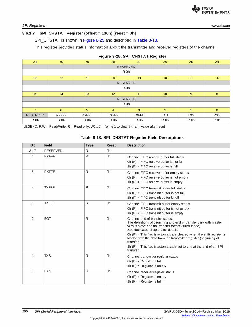
SPI Registers www.ti.com
280 SWRU367D–June 2014–Revised May 2018Submit Documentation Feedback
Copyright © 2014–2018, Texas Instruments Incorporated
SPI (Serial Peripheral Interface)
8.6.1.7 SPI_CHSTAT Register (offset = 130h) [reset = 0h]SPI_CHSTAT is shown in Figure 8-25 and described in Table 8-13.
This register provides status information about the transmitter and receiver registers of the channel.
Figure 8-25. SPI_CHSTAT Register31 30 29 28 27 26 25 24
RESERVEDR-0h
23 22 21 20 19 18 17 16RESERVED
R-0h
15 14 13 12 11 10 9 8RESERVED
R-0h
7 6 5 4 3 2 1 0RESERVED RXFFF RXFFE TXFFF TXFFE EOT TXS RXS
R-0h R-0h R-0h R-0h R-0h R-0h R-0h R-0h
LEGEND: R/W = Read/Write; R = Read only; W1toCl = Write 1 to clear bit; -n = value after reset
Table 8-13. SPI_CHSTAT Register Field Descriptions
Bit Field Type Reset Description31-7 RESERVED R 0h
6 RXFFF R 0h Channel FIFO receive buffer full status0h (R) = FIFO receive buffer is not full1h (R) = FIFO receive buffer is full
5 RXFFE R 0h Channel FIFO receive buffer empty status0h (R) = FIFO receive buffer is not empty1h (R) = FIFO receive buffer is empty
4 TXFFF R 0h Channel FIFO transmit buffer full status0h (R) = FIFO transmit buffer is not full1h (R) = FIFO transmit buffer is full
3 TXFFE R 0h Channel FIFO transmit buffer empty status0h (R) = FIFO transmit buffer is not empty1h (R) = FIFO transmit buffer is empty
2 EOT R 0h Channel end of transfer status.The definitions of beginning and end of transfer vary with masterversus slave and the transfer format (turbo mode).See dedicated chapters for details.0h (R) = This flag is automatically cleared when the shift register isloaded with the data from the transmitter register (beginning oftransfer).1h (R) = This flag is automatically set to one at the end of an SPItransfer.
1 TXS R 0h Channel transmitter register status0h (R) = Register is full1h (R) = Register is empty
0 RXS R 0h Channel receiver register status0h (R) = Register is empty1h (R) = Register is full
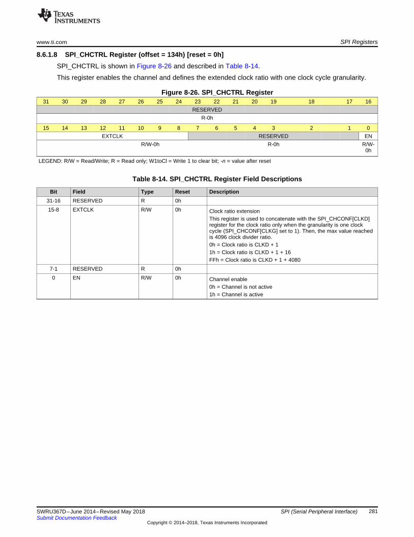
www.ti.com SPI Registers
281SWRU367D–June 2014–Revised May 2018Submit Documentation Feedback
Copyright © 2014–2018, Texas Instruments Incorporated
SPI (Serial Peripheral Interface)
8.6.1.8 SPI_CHCTRL Register (offset = 134h) [reset = 0h]SPI_CHCTRL is shown in Figure 8-26 and described in Table 8-14.
This register enables the channel and defines the extended clock ratio with one clock cycle granularity.
Figure 8-26. SPI_CHCTRL Register31 30 29 28 27 26 25 24 23 22 21 20 19 18 17 16
RESERVEDR-0h
15 14 13 12 11 10 9 8 7 6 5 4 3 2 1 0EXTCLK RESERVED EN
R/W-0h R-0h R/W-0h
LEGEND: R/W = Read/Write; R = Read only; W1toCl = Write 1 to clear bit; -n = value after reset
Table 8-14. SPI_CHCTRL Register Field Descriptions
Bit Field Type Reset Description31-16 RESERVED R 0h15-8 EXTCLK R/W 0h Clock ratio extension
This register is used to concatenate with the SPI_CHCONF[CLKD]register for the clock ratio only when the granularity is one clockcycle (SPI_CHCONF[CLKG] set to 1). Then, the max value reachedis 4096 clock divider ratio.0h = Clock ratio is CLKD + 11h = Clock ratio is CLKD + 1 + 16FFh = Clock ratio is CLKD + 1 + 4080
7-1 RESERVED R 0h0 EN R/W 0h Channel enable
0h = Channel is not active1h = Channel is active
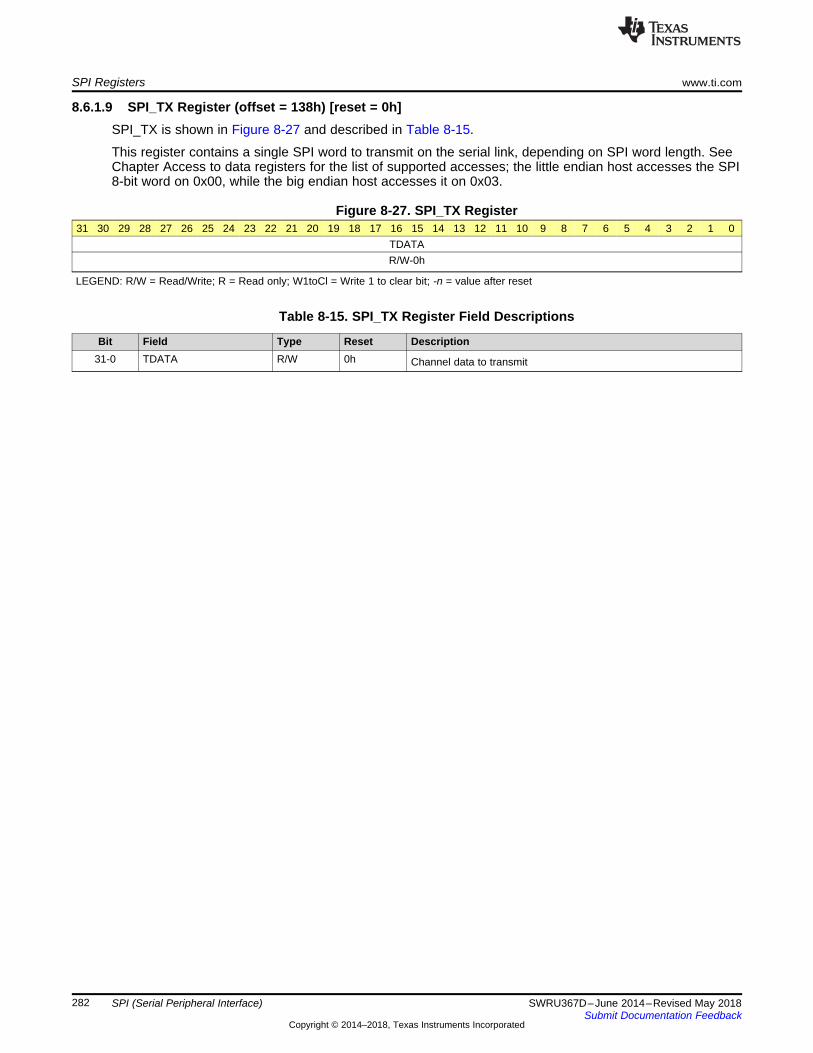
SPI Registers www.ti.com
282 SWRU367D–June 2014–Revised May 2018Submit Documentation Feedback
Copyright © 2014–2018, Texas Instruments Incorporated
SPI (Serial Peripheral Interface)
8.6.1.9 SPI_TX Register (offset = 138h) [reset = 0h]SPI_TX is shown in Figure 8-27 and described in Table 8-15.
This register contains a single SPI word to transmit on the serial link, depending on SPI word length. SeeChapter Access to data registers for the list of supported accesses; the little endian host accesses the SPI8-bit word on 0x00, while the big endian host accesses it on 0x03.
Figure 8-27. SPI_TX Register31 30 29 28 27 26 25 24 23 22 21 20 19 18 17 16 15 14 13 12 11 10 9 8 7 6 5 4 3 2 1 0
TDATAR/W-0h
LEGEND: R/W = Read/Write; R = Read only; W1toCl = Write 1 to clear bit; -n = value after reset
Table 8-15. SPI_TX Register Field Descriptions
Bit Field Type Reset Description31-0 TDATA R/W 0h Channel data to transmit
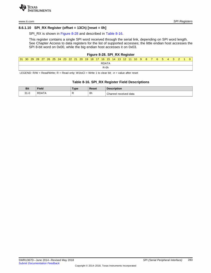
www.ti.com SPI Registers
283SWRU367D–June 2014–Revised May 2018Submit Documentation Feedback
Copyright © 2014–2018, Texas Instruments Incorporated
SPI (Serial Peripheral Interface)
8.6.1.10 SPI_RX Register (offset = 13Ch) [reset = 0h]SPI_RX is shown in Figure 8-28 and described in Table 8-16.
This register contains a single SPI word received through the serial link, depending on SPI word length.See Chapter Access to data registers for the list of supported accesses; the little endian host accesses theSPI 8-bit word on 0x00, while the big endian host accesses it on 0x03.
Figure 8-28. SPI_RX Register31 30 29 28 27 26 25 24 23 22 21 20 19 18 17 16 15 14 13 12 11 10 9 8 7 6 5 4 3 2 1 0
RDATAR-0h
LEGEND: R/W = Read/Write; R = Read only; W1toCl = Write 1 to clear bit; -n = value after reset
Table 8-16. SPI_RX Register Field Descriptions
Bit Field Type Reset Description31-0 RDATA R 0h Channel received data
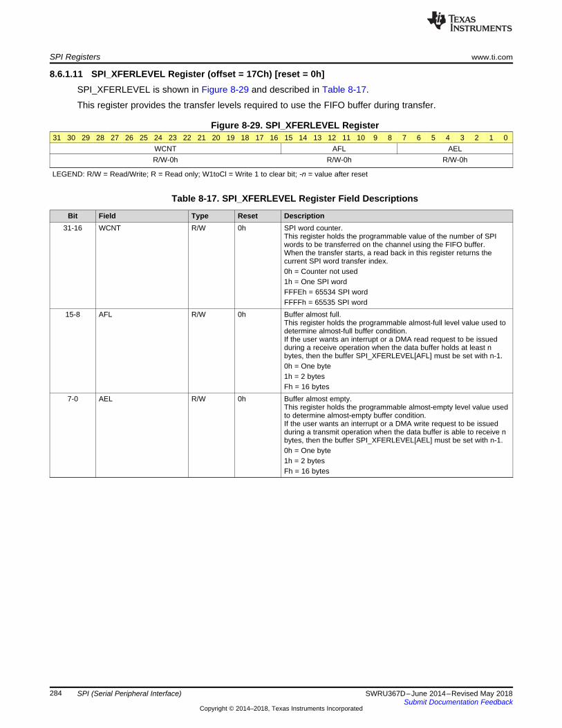
SPI Registers www.ti.com
284 SWRU367D–June 2014–Revised May 2018Submit Documentation Feedback
Copyright © 2014–2018, Texas Instruments Incorporated
SPI (Serial Peripheral Interface)
8.6.1.11 SPI_XFERLEVEL Register (offset = 17Ch) [reset = 0h]SPI_XFERLEVEL is shown in Figure 8-29 and described in Table 8-17.
This register provides the transfer levels required to use the FIFO buffer during transfer.
Figure 8-29. SPI_XFERLEVEL Register31 30 29 28 27 26 25 24 23 22 21 20 19 18 17 16 15 14 13 12 11 10 9 8 7 6 5 4 3 2 1 0
WCNT AFL AELR/W-0h R/W-0h R/W-0h
LEGEND: R/W = Read/Write; R = Read only; W1toCl = Write 1 to clear bit; -n = value after reset
Table 8-17. SPI_XFERLEVEL Register Field Descriptions
Bit Field Type Reset Description31-16 WCNT R/W 0h SPI word counter.
This register holds the programmable value of the number of SPIwords to be transferred on the channel using the FIFO buffer.When the transfer starts, a read back in this register returns thecurrent SPI word transfer index.0h = Counter not used1h = One SPI wordFFFEh = 65534 SPI wordFFFFh = 65535 SPI word
15-8 AFL R/W 0h Buffer almost full.This register holds the programmable almost-full level value used todetermine almost-full buffer condition.If the user wants an interrupt or a DMA read request to be issuedduring a receive operation when the data buffer holds at least nbytes, then the buffer SPI_XFERLEVEL[AFL] must be set with n-1.0h = One byte1h = 2 bytesFh = 16 bytes
7-0 AEL R/W 0h Buffer almost empty.This register holds the programmable almost-empty level value usedto determine almost-empty buffer condition.If the user wants an interrupt or a DMA write request to be issuedduring a transmit operation when the data buffer is able to receive nbytes, then the buffer SPI_XFERLEVEL[AEL] must be set with n-1.0h = One byte1h = 2 bytesFh = 16 bytes
285SWRU367D–June 2014–Revised May 2018Submit Documentation Feedback
Copyright © 2014–2018, Texas Instruments Incorporated
General-Purpose Timers
Chapter 9SWRU367D–June 2014–Revised May 2018
General-Purpose Timers
Topic ........................................................................................................................... Page
9.1 Overview ......................................................................................................... 2869.2 Block Diagram.................................................................................................. 2869.3 Functional Description ...................................................................................... 2879.4 Initialization and Configuration .......................................................................... 2949.5 TIMER Registers............................................................................................... 297
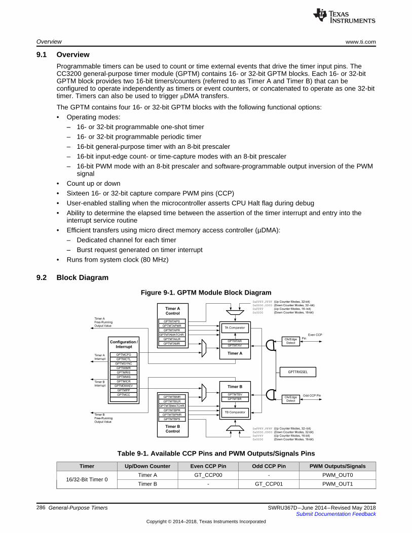
GPTTRIGSEL
GPTMTAPS
GPTMTAPMR
GPTMTAPR
GPTMTAMATCHR
GPTMTAILR
GPTMTAMR
GPTMTBMR
GPTMTBILR
GPTMTBMATCHR
GPTMTBPR
GPTMTBPMR
GPTMTBPS
Timer A
Free-Running
Output Value
Timer A
Control
TA Comparator
0xFFFF.FFFF (Up Counter Modes, 32-bit)
0x0000.0000 (Down Counter Modes, 32--bit)
0xFFFF (Up Counter Modes, 16--bit)
0x0000 (Down Counter Modes, 16-bit)
Timer A
Interrupt
Timer B
Interrupt
Configuration /
Interrupt
GPTMCFG
GPTMCTL
GPTMSYNC
GPTMIMR
GPTMRIS
GPTMMIS
GPTMICR
GPTMDMAEV
GPTMPP
GPTMCC
GPTMTAR
GPTMTAV
Timer A
Timer B
GPTMTBV
GPTMTBR
Clk/Edge
Detect
Clk/Edge
Detect
Even CCP
Pin
Odd CCP Pin
Timer B
Free-Running
Output Value
Timer B
Control
TB Comparator
0xFFFF.FFFF (Up Counter Modes, 32--bit)
0x0000.0000 (Down Counter Modes, 32-bit)
0xFFFF (Up Counter Modes, 16-bit)
0x0000 (Down Counter Modes, 16-bit)
Overview www.ti.com
286 SWRU367D–June 2014–Revised May 2018Submit Documentation Feedback
Copyright © 2014–2018, Texas Instruments Incorporated
General-Purpose Timers
9.1 OverviewProgrammable timers can be used to count or time external events that drive the timer input pins. TheCC3200 general-purpose timer module (GPTM) contains 16- or 32-bit GPTM blocks. Each 16- or 32-bitGPTM block provides two 16-bit timers/counters (referred to as Timer A and Timer B) that can beconfigured to operate independently as timers or event counters, or concatenated to operate as one 32-bittimer. Timers can also be used to trigger μDMA transfers.
The GPTM contains four 16- or 32-bit GPTM blocks with the following functional options:• Operating modes:
– 16- or 32-bit programmable one-shot timer– 16- or 32-bit programmable periodic timer– 16-bit general-purpose timer with an 8-bit prescaler– 16-bit input-edge count- or time-capture modes with an 8-bit prescaler– 16-bit PWM mode with an 8-bit prescaler and software-programmable output inversion of the PWM
signal• Count up or down• Sixteen 16- or 32-bit capture compare PWM pins (CCP)• User-enabled stalling when the microcontroller asserts CPU Halt flag during debug• Ability to determine the elapsed time between the assertion of the timer interrupt and entry into the
interrupt service routine• Efficient transfers using micro direct memory access controller (µDMA):
– Dedicated channel for each timer– Burst request generated on timer interrupt
• Runs from system clock (80 MHz)
9.2 Block Diagram
Figure 9-1. GPTM Module Block Diagram
Table 9-1. Available CCP Pins and PWM Outputs/Signals Pins
Timer Up/Down Counter Even CCP Pin Odd CCP Pin PWM Outputs/Signals
16/32-Bit Timer 0Timer A GT_CCP00 - PWM_OUT0Timer B - GT_CCP01 PWM_OUT1
www.ti.com Functional Description
287SWRU367D–June 2014–Revised May 2018Submit Documentation Feedback
Copyright © 2014–2018, Texas Instruments Incorporated
General-Purpose Timers
Table 9-1. Available CCP Pins and PWM Outputs/Signals Pins (continued)Timer Up/Down Counter Even CCP Pin Odd CCP Pin PWM Outputs/Signals
16/32-Bit Timer 1Timer A GT_CCP02 - PWM_OUT2Timer B - GT_CCP03 PWM_OUT3
16/32-Bit Timer 2Timer A GT_CCP04 -Timer B - GT_CCP05 PWM_OUT5
16/32-Bit Timer 3Timer A GT_CCP06 - PWM_OUT6Timer B - GT_CCP07 PWM_OUT7
The GP timer signals pin-muxed and CONFMODE bits in the GPIO PAD CONFIG register should be setto choose the GP timer function.
9.3 Functional DescriptionThe main components of each GPTM block are two free-running up/down counters (referred to as Timer Aand Timer B), two prescaler registers, two match registers, two prescaler match registers, two shadowregisters, and two load/initialization registers and their associated control functions. The exact functionalityof each GPTM is controlled by software and configured through the register interface. Timer A and TimerB can be used individually, in which case they have a 16-bit counting range for the 16/32-bit GPTMblocks. In addition, Timer A and Timer B can be concatenated to provide a 32-bit counting range for the16/32-bit GPTM blocks.
NOTE: The prescaler can only be used when the timers are used individually.
The available modes for each GPTM block are shown in Table 9-2. Note that when counting down in one-shot or periodic modes, the prescaler acts as a true prescaler and contains the least-significant bits of thecount. When counting up in one-shot or periodic modes, the prescaler acts as a timer extension, andholds the most-significant bits of the count. In input edge count, input edge time, and PWM mode, theprescaler always acts as a timer extension, regardless of the count direction.
(1) The prescaler is only available when the timers are used individually
Table 9-2. General-Purpose Timer Capabilities
Mode Timer Use Count Direction Counter Size Prescaler Size (1)
One-shotIndividual Up or down 16-bit 8-bit
Concatenated Up or down 32-bit -
PeriodicIndividual Up or down 16-bit 8-bit
Concatenated Up or down 32-bit -Edge Count Individual Up or down 16-bit 8-bitEdge Time Individual Up or down 16-bit 8-bit
PWM Individual Down 16-bit 8-bit
Software configures the GPTM using the GPTM Configuration (GPTMCFG) register, the GPTM Timer AMode (GPTMTAMR) register, and the GPTM Timer B Mode (GPTMTBMR) register. When in one of theconcatenated modes, Timer A and Timer B can only operate in one mode. However, when configured inan individual mode, Timer A and Timer B can be independently configured in any combination of theindividual modes.
9.3.1 GPTM Reset ConditionsAfter reset has been applied to the GPTM module, the module is in an inactive state, and all controlregisters are cleared and in their default states. Counters Timer A and Timer B are initialized to all 1s,along with their corresponding registers:
Load registers:• GPTM Timer A Interval Load (GPTMTAILR) register
Functional Description www.ti.com
288 SWRU367D–June 2014–Revised May 2018Submit Documentation Feedback
Copyright © 2014–2018, Texas Instruments Incorporated
General-Purpose Timers
• GPTM Timer B Interval Load (GPTMTBILR) register
Shadow registers:• GPTM Timer A Value (GPTMTAV) register• GPTM Timer B Value (GPTMTBV) register
The following prescale counters are initialized to all 0s:• GPTM Timer A Prescale (GPTMTAPR) register• GPTM Timer B Prescale (GPTMTBPR) register• GPTM Timer A Prescale Snapshot (GPTMTAPS) register• GPTM Timer B Prescale Snapshot (GPTMTBPS) register
9.3.2 Timer ModesThis section describes the operation of the various timer modes. When using Timer A and Timer B inconcatenated mode, only the Timer A control and status bits must be used; there is no need to use TimerB control and status bits. The GPTM is placed into individual/split mode by writing a value of 0x4 to theGPTM Configuration (GPTMCFG) register. In the following sections, the variable n is used in bit field andregister names to imply either a Timer A function or a Timer B function. Throughout this section, thetimeout event in down-count mode is 0x0, and in up-count mode is the value in the GPTM Timer n IntervalLoad (GPTMTnILR) and the optional GPTM Timer n Prescale (GPTMTnPR) registers.
9.3.2.1 One-Shot or Periodic Timer ModeThe selection of one-shot or periodic mode is determined by the value written to the TnMR field of theGPTM Timer n Mode (GPTMTnMR) register. The timer is configured to count up or down using theTnCDIR bit in the GPTMTnMR register.
When software sets the TnEN bit in the GPTM Control (GPTMCTL) register, the timer begins counting upfrom 0x0 or down from its preloaded value. Table 9-3 shows the values loaded into the timer registerswhen the timer is enabled.
Table 9-3. Counter Values When the Timer is Enabled in Periodic or One-Shot Modes
Register Count Down Mode Count Up ModeGPTMTnR GPTMTnILR 0x0
GPTMTnVGPTMTnILR in concatenated mode;
GPTMTnPR in combination withGPTMTnILR in individual mode.
0x0
GPTMTnPS GPTMTnPR in individual mode; notavailable in concatenated mode.
0x0 in individual mode; not available inconcatenated mode.
When the timer is counting down and it reaches the timeout event (0x0), the timer reloads its start valuefrom the GPTMTnILR and the GPTMTnPR registers on the next cycle. When the timer is counting up andit reaches the timeout event (the value in the GPTMTnILR and the optional GPTMTnPR registers), thetimer reloads with 0x0. If configured as a one-shot timer, the timer stops counting and clears the TnEN bitin the GPTMCTL register. If configured as a periodic timer, the timer starts counting again on the nextcycle.
In periodic, snap-shot mode, the TnMR field is 0x2 and the TnSNAPS bit is set in the GPTMTnMRregister, the value of the timer at the time-out event is loaded into the GPTMTnR register, and the value ofthe prescaler is loaded into the GPTMTnPS register. The free-running counter value is shown in theGPTMTnV register. In this manner, software can determine the time elapsed from the interrupt assertionto the ISR entry by examining the snapshot values and the current value of the free-running timer.Snapshot mode is not available when the timer is configured in one-shot mode.
www.ti.com Functional Description
289SWRU367D–June 2014–Revised May 2018Submit Documentation Feedback
Copyright © 2014–2018, Texas Instruments Incorporated
General-Purpose Timers
In addition to reloading the count value, the GPTM can generate interrupts, CCP outputs, and triggerswhen it reaches the time-out event. The GPTM sets the TnTORIS bit in the GPTM Raw Interrupt Status(GPTMRIS) register, and holds it until it is cleared by writing the GPTM Interrupt Clear (GPTMICR)register. If the time-out interrupt is enabled in the GPTM Interrupt Mask (GPTMIMR) register, the GPTMalso sets the TnTOMIS bit in the GPTM Masked Interrupt Status (GPTMMIS) register. The time-outinterrupt can be disabled entirely by setting the TACINTD bit in the GPTM Timer n Mode (GPTMTnMR)register. In this case, the TnTORIS bit does not even set in the GPTMRIS register.
By setting the TnMIE bit in the GPTMTnMR register, an interrupt condition can also be generated whenthe timer value equals the value loaded into the GPTM Timer n Match (GPTMTnMATCHR) and GPTMTimer n Prescale Match (GPTMTnPMR) registers. This interrupt has the same status, masking, andclearing functions as the time-out interrupt, but uses the match interrupt bits instead (for example, the rawinterrupt status is monitored using the TnMRIS bit in the GPTM Raw Interrupt Status (GPTMRIS) register).The interrupt status bits are not updated by the hardware unless the TnMIE bit in the GPTMTnMR registeris set, which is different than the behavior for the time-out interrupt. The μDMA trigger is enabled byconfiguring and enabling the appropriate μDMA channel, as well as the type of trigger enable in the GPTMDMA Event (GPTMDMAEV) register.
If software updates the GPTMTnILR or the GPTMTnPR register while the counter is counting down, thecounter loads the new value on the next clock cycle and continues counting from the new value if theTnILD bit in the GPTMTnMR register is clear. If the TnILD bit is set, the counter loads the new value afterthe next timeout. If software updates the GPTMTnILR or the GPTMTnPR register while the counter iscounting up, the timeout event is changed on the next cycle to the new value. If software updates theGPTM Timer n Value (GPTMTnV) register while the counter is counting up or down, the counter loads thenew value on the next clock cycle and continues counting from the new value. If software updates theGPTMTnMATCHR or the GPTMTnPMR registers, the new values are reflected on the next clock cycle ifthe TnMRSU bit in the GPTMTnMR register is clear. If the TnMRSU bit is set, the new value does not takeeffect until the next timeout.
If the TnSTALL bit in the GPTMCTL register is set, the timer freezes counting while the processor ishalted by the debugger. The timer resumes counting when the processor resumes execution.
Table 9-4 shows a variety of configurations for a 16-bit free-running timer while using the prescaler. Allvalues assume a 80-MHz clock with Tc=12.5 ns (clock period). The prescaler can only be used when a16/32-bit timer is configured in 16-bit mode.
(1) Tc is the clock period.
Table 9-4. 16-Bit Timer With Prescaler Configurations
Prescale (8-bit value) Number of Timer Clocks(Tc) (1) Max Time Units
00000000 1 0.8192 ms00000001 2 1.6384 ms00000010 3 2.4576 ms------------ -- -- --11111101 254 208.0768 ms11111110 255 208.896 ms11111111 256 209.7152 ms
9.3.2.2 Input Edge-Count Mode
NOTE: For rising-edge detection, the input signal must be High for at least two clock periodsfollowing the rising edge. Similarly, for falling-edge detection, the input signal must be Lowfor at least two clock periods following the falling edge. Based on this criteria, the maximuminput frequency for edge detection is 1/4 of the frequency.
Functional Description www.ti.com
290 SWRU367D–June 2014–Revised May 2018Submit Documentation Feedback
Copyright © 2014–2018, Texas Instruments Incorporated
General-Purpose Timers
In edge-count mode, the timer is configured as a 24-bit up- or down-counter, including the optionalprescaler with the upper count value stored in the GPTM Timer n Prescale (GPTMTnPR) register and thelower bits in the GPTMTnR register. In this mode, the timer is capable of capturing three types of events:rising edge, falling edge, or both. To place the timer in edge-count mode, the TnCMR bit of theGPTMTnMR register must be cleared. The type of edge that the timer counts is determined by theTnEVENT fields of the GPTMCTL register. During initialization in down-count mode, theGPTMTnMATCHR and GPTMTnPMR registers are configured so that the difference between the value inthe GPTMTnILR and GPTMTnPR registers and the GPTMTnMATCHR and GPTMTnPMR registers equalsthe number of edge events that must be counted. In up-count mode, the timer counts from 0x0 to thevalue in the GPTMTnMATCHR and GPTMTnPMR registers. Note that when executing an up-count, thevalue of GPTMTnPR and GPTMTnILR must be greater than the value of GPTMTnPMR andGPTMTnMATCHR. Table 9-5 shows the values loaded into the timer registers when the timer is enabled.
Table 9-5. Counter Values When the Timer is Enabled in Input Edge-Count Mode
Register Count Down Mode Count Up Mode
GPTMTnR GPTMTnPR in combination withGPTMTnILR 0x0
GPTMTnV GPTMTnPR in combination withGPTMTnILR 0x0
When software writes the TnEN bit in the GPTM Control (GPTMCTL) register, the timer is enabled forevent capture. Each input event on the CCP pin decrements or increments the counter by 1 until the eventcount matches GPTMTnMATCHR and GPTMTnPMR. When the counts match, the GPTM asserts theCnMRIS bit in the GPTM Raw Interrupt Status (GPTMRIS) register, and holds it until it is cleared bywriting the GPTM Interrupt Clear (GPTMICR) register. If the capture mode match interrupt is enabled inthe GPTM Interrupt Mask (GPTMIMR) register, the GPTM also sets the CnMMIS bit in the GPTM MaskedInterrupt Status (GPTMMIS) register. In up-count mode, the current count of the input events is held inboth the GPTMTnR and GPTMTnV registers. In down-count mode, the current count of the input eventscan be obtained by subtracting the GPTMTnR or GPTMTnV from the value made up of the GPTMTnPRand GPTMTnILR register combination.
The μDMA trigger is enabled by configuring and enabling the appropriate μDMA channel, as well as thetype of trigger enable in the GPTM DMA Event (GPTMDMAEV) register.
After the match value is reached in down-count mode, the counter is then reloaded using the value in theGPTMTnILR and GPTMTnPR registers, and stopped because the GPTM automatically clears the TnENbit in the GPTMCTL register. Once the event count has been reached, all further events are ignored untilTnEN is re-enabled by software. In up-count mode, the timer is reloaded with 0x0 and continues counting.
Figure 9-2 shows how input edge-count mode works. In this case, the timer start value is set toGPTMTnILR =0x000A, and the match value is set to GPTMTnMATCHR =0x0006 so that four edge eventsare counted. The counter is configured to detect both edges of the input signal.
The last two edges are not counted, because the timer automatically clears the TnEN bit after the currentcount matches the value in the GPTMTnMATCHR register.

www.ti.com Functional Description
291SWRU367D–June 2014–Revised May 2018Submit Documentation Feedback
Copyright © 2014–2018, Texas Instruments Incorporated
General-Purpose Timers
Figure 9-2. Input Edge-Count Mode Example, Counting Down
9.3.2.3 Input Edge-Time Mode
NOTE: For rising-edge detection, the input signal must be High for at least two system clockperiods following the rising edge. Similarly, for falling edge detection, the input signal mustbe Low for at least two system clock periods following the falling edge. Based on this criteria,the maximum input frequency for edge detection is 1/4 of the system frequency.
In edge-time mode, the timer is configured as a 24-bit up- or down-counter, including the optionalprescaler with the upper timer value stored in the GPTMTnPR register and the lower bits in theGPTMTnILR register. In this mode, the timer is initialized to the value loaded in the GPTMTnILR andGPTMTnPR registers when counting down, and 0x0 when counting up. The timer is capable of capturingthree types of events: rising edge, falling edge, or both. The timer is placed into edge-time mode bysetting the TnCMR bit in the GPTMTnMR register, and the type of event that the timer captures isdetermined by the TnEVENT fields of the GPTMCTL register. Table 9-6 shows the values loaded into thetimer registers when the timer is enabled.
Set the TRIGSEL bits of the register GPTTRIGSEL to detect GPIO triggers.
Table 9-6. Counter Values When the Timer is Enabled in Input Event-Count Mode
Register Count Down Mode Count Up ModeTnR GPTMTnILR 0x0TnV GPTMTnILR 0x0
When software writes the TnEN bit in the GPTMCTL register, the timer is enabled for event capture. Whenthe selected input event is detected, the current timer counter value is captured in the GPTMTnR andGPTMTnPS registers, and is available to be read by the microcontroller. The GPTM then asserts theCnERIS bit in the GPTM Raw Interrupt Status (GPTMRIS) register, and holds it until it is cleared by writingthe GPTM Interrupt Clear (GPTMICR) register. If the capture mode event interrupt is enabled in the GPTMInterrupt Mask (GPTMIMR) register, the GPTM also sets the CnEMIS bit in the GPTM Masked InterruptStatus (GPTMMIS) register. In this mode, the GPTMTnR and GPTMTnPS registers hold the time at whichthe selected input event occurred, while the GPTMTnV register holds the free-running timer value. Theseregisters can be read to determine the time that elapsed between the interrupt assertion and the entry intothe ISR.
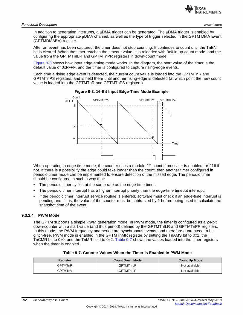
Functional Description www.ti.com
292 SWRU367D–June 2014–Revised May 2018Submit Documentation Feedback
Copyright © 2014–2018, Texas Instruments Incorporated
General-Purpose Timers
In addition to generating interrupts, a μDMA trigger can be generated. The μDMA trigger is enabled byconfiguring the appropriate μDMA channel, as well as the type of trigger selected in the GPTM DMA Event(GPTMDMAEV) register.
After an event has been captured, the timer does not stop counting. It continues to count until the TnENbit is cleared. When the timer reaches the timeout value, it is reloaded with 0x0 in up-count mode, and thevalue from the GPTMTnILR and GPTMTnPR registers in down-count mode.
Figure 9-3 shows how input edge-timing mode works. In the diagram, the start value of the timer is thedefault value of 0xFFFF, and the timer is configured to capture rising-edge events.
Each time a rising edge event is detected, the current count value is loaded into the GPTMTnR andGPTMTnPS registers, and is held there until another rising-edge is detected (at which point the new countvalue is loaded into the GPTMTnR and GPTMTnPS registers).
Figure 9-3. 16-Bit Input Edge-Time Mode Example
When operating in edge-time mode, the counter uses a modulo 224 count if prescaler is enabled, or 216 ifnot. If there is a possibility the edge could take longer than the count, then another timer configured inperiodic-timer mode can be implemented to ensure detection of the missed edge. The periodic timershould be configured in such a way that:• The periodic timer cycles at the same rate as the edge-time timer.• The periodic timer interrupt has a higher interrupt priority than the edge-time timeout interrupt.• If the periodic timer interrupt service routine is entered, software must check if an edge-time interrupt is
pending and if it is, the value of the counter must be subtracted by 1 before being used to calculate thesnapshot time of the event.
9.3.2.4 PWM ModeThe GPTM supports a simple PWM generation mode. In PWM mode, the timer is configured as a 24-bitdown-counter with a start value (and thus period) defined by the GPTMTnILR and GPTMTnPR registers.In this mode, the PWM frequency and period are synchronous events, and therefore guaranteed to beglitch-free. PWM mode is enabled in the GPTMTnMR register by setting the TnAMS bit to 0x1, theTnCMR bit to 0x0, and the TnMR field to 0x2. Table 9-7 shows the values loaded into the timer registerswhen the timer is enabled.
Table 9-7. Counter Values When the Timer is Enabled in PWM Mode
Register Count Down Mode Count Up ModeGPTMTnR GPTMTnILR Not availableGPTMTnV GPTMTnILR Not available
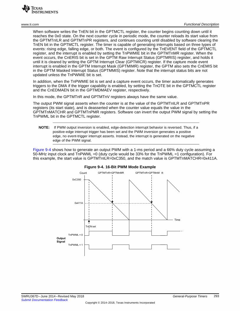
www.ti.com Functional Description
293SWRU367D–June 2014–Revised May 2018Submit Documentation Feedback
Copyright © 2014–2018, Texas Instruments Incorporated
General-Purpose Timers
When software writes the TnEN bit in the GPTMCTL register, the counter begins counting down until itreaches the 0x0 state. On the next counter cycle in periodic mode, the counter reloads its start value fromthe GPTMTnILR and GPTMTnPR registers, and continues counting until disabled by software clearing theTnEN bit in the GPTMCTL register. The timer is capable of generating interrupts based on three types ofevents: rising edge, falling edge, or both. The event is configured by the TnEVENT field of the GPTMCTLregister, and the interrupt is enabled by setting the TnPWMIE bit in the GPTMTnMR register. When theevent occurs, the CnERIS bit is set in the GPTM Raw Interrupt Status (GPTMRIS) register, and holds ituntil it is cleared by writing the GPTM Interrupt Clear (GPTMICR) register. If the capture mode eventinterrupt is enabled in the GPTM Interrupt Mask (GPTMIMR) register, the GPTM also sets the CnEMIS bitin the GPTM Masked Interrupt Status (GPTMMIS) register. Note that the interrupt status bits are notupdated unless the TnPWMIE bit is set.
In addition, when the TnPWMIE bit is set and a capture event occurs, the timer automatically generatestriggers to the DMA if the trigger capability is enabled, by setting the TnOTE bit in the GPTMCTL registerand the CnEDMAEN bit in the GPTMDMAEV register, respectively.
In this mode, the GPTMTnR and GPTMTnV registers always have the same value.
The output PWM signal asserts when the counter is at the value of the GPTMTnILR and GPTMTnPRregisters (its start state), and is deasserted when the counter value equals the value in theGPTMTnMATCHR and GPTMTnPMR registers. Software can invert the output PWM signal by setting theTnPWML bit in the GPTMCTL register.
NOTE: If PWM output inversion is enabled, edge-detection interrupt behavior is reversed. Thus, if apositive-edge interrupt trigger has been set and the PWM inversion generates a positiveedge, no event-trigger interrupt asserts. Instead, the interrupt is generated on the negativeedge of the PWM signal.
Figure 9-4 shows how to generate an output PWM with a 1-ms period and a 66% duty cycle assuming a50-MHz input clock and TnPWML =0 (duty cycle would be 33% for the TnPWML =1 configuration). Forthis example, the start value is GPTMTnILR=0xC350, and the match value is GPTMTnMATCHR=0x411A.
Figure 9-4. 16-Bit PWM Mode Example
Functional Description www.ti.com
294 SWRU367D–June 2014–Revised May 2018Submit Documentation Feedback
Copyright © 2014–2018, Texas Instruments Incorporated
General-Purpose Timers
9.3.3 DMA OperationThe timers each have a dedicated μDMA channel and can provide a request signal to the μDMAcontroller. Pulse requests are generated by a timer using its own dma_req signal. A dma_done signal isprovided from the µDMA to each timer, to indicate transfer completion and trigger a µDMA done interrupt(DMAnRIS) in the GPTM Raw Interrupt Status Register (GPTMRIS) register. The request is a burst type,and occurs whenever a timer raw interrupt condition occurs. The arbitration size of the μDMA transfershould be set to the amount of data that should be transferred whenever a timer event occurs.
For example, to transfer 256 items, or 8 items at a time every 10 ms, configure a timer to generate aperiodic timeout at 10 ms. Configure the μDMA transfer for a total of 256 items, with a burst size of 8items. Each time the timer times out, the μDMA controller transfers 8 items, until all 256 items have beentransferred.
The GPTM DMA Event (GPTMDMAEV) register enables the types of events that can cause a dma_reqsignal assertion by the timer module. Application software can enable a dma_req trigger for a match,capture, or time-out event for each timer using the GPTMDMAEV register. For an individual timer, allactive timer trigger events that have been enabled through the GPTMDMAEV register are ORed togetherto create a single dma_req pulse that is sent to the µDMA. When the µDMA transfer has completed, adma_done signal is sent to the timer, resulting in a DMAnRIS bit set in the GPTMRIS register.
9.3.4 Accessing Concatenated 16/32-Bit GPTM Register ValuesThe GPTM is placed into concatenated mode by writing a 0x0 to the GPTMCFG bit field in the GPTMConfiguration (GPTMCFG) register. In this configuration, certain 16/32-bit GPTM registers areconcatenated to form pseudo-32-bit registers. These registers include:• GPTM Timer A Interval Load (GPTMTAILR) register [15:0]• GPTM Timer B Interval Load (GPTMTBILR) register [15:0]• GPTM Timer A (GPTMTAR) register [15:0]• GPTM Timer B (GPTMTBR) register [15:0]• GPTM Timer A Value (GPTMTAV) register [15:0]• GPTM Timer B Value (GPTMTBV) register [15:0]• GPTM Timer A Match (GPTMTAMATCHR) register [15:0]• GPTM Timer B Match (GPTMTBMATCHR) register [15:0]
In the 32-bit modes, the GPTM translates a 32-bit write access to GPTMTAILR into a write access to bothGPTMTAILR and GPTMTBILR. The resulting word ordering for such a write operation is:GPTMTBILR[15:0]:GPTMTAILR[15:0]
Likewise, a 32-bit read access to GPTMTAR returns the value:GPTMTBR[15:0]:GPTMTAR[15:0]
A 32-bit read access to GPTMTAV returns the value:GPTMTBV[15:0]:GPTMTAV[15:0]
9.4 Initialization and ConfigurationTo use a GPTM, the appropriate CLKEN bit must be set in the GPTnCLKCFG or GPTnCLKEN register.Configure the CONFMODE fields in the GPIO_PAD_CONFIG register to assign the CCP signals to theappropriate pins. The user should set GPTTRIGSEL bits appropriately before using CCP mode.
The user can also reset GPTM blocks using register GPTnSWRST.
This section shows module initialization and configuration examples for each of the supported timermodes.
9.4.1 One-Shot and Periodic Timer ModeThe GPTM is configured for one-shot and periodic modes by the following sequence:1. Ensure the timer is disabled (the TnEN bit in the GPTMCTL register is cleared) before making any
www.ti.com Initialization and Configuration
295SWRU367D–June 2014–Revised May 2018Submit Documentation Feedback
Copyright © 2014–2018, Texas Instruments Incorporated
General-Purpose Timers
changes.2. Write the GPTM Configuration Register (GPTMCFG) with a value of 0x0000.0000.3. Configure the TnMR field in the GPTM Timer n Mode Register (GPTMTnMR):
a. Write a value of 0x1 for one-shot mode.b. Write a value of 0x2 for periodic mode.
4. Optionally configure the TnSNAPS, TnWOT, TnMTE, and TnCDIR bits in the GPTMTnMR register toselect whether to capture the value of the free-running timer at time-out, use an external trigger to startcounting, configure an additional trigger or interrupt, and count up or down.
5. Load the start value into the GPTM Timer n Interval Load (GPTMTnILR) register.6. If interrupts are required, set the appropriate bits in the GPTM Interrupt Mask (GPTMIMR) register.7. Set the TnEN bit in the GPTMCTL register to enable the timer and start counting.8. Poll the GPTMRIS register or wait for the interrupt to be generated (if enabled). In both cases, the
status flags are cleared by writing a 1 to the appropriate bit of the GPTM Interrupt Clear (GPTMICR)register.
If the TnMIE bit in the GPTMTnMR register is set, the RTCRIS bit in the GPTMRIS register is set, and thetimer continues counting. In one-shot mode, the timer stops counting after the time-out event. To re-enable the timer, repeat the sequence. A timer configured in periodic mode reloads the timer andcontinues counting after the time-out event.
9.4.2 Input Edge-Count ModeConfigure the timer to input edge-count mode with the following sequence:1. Ensure the timer is disabled (the TnEN bit is cleared) before making any changes.2. Write the GPTM Configuration (GPTMCFG) register with a value of 0x0000.0004.3. In the GPTM Timer Mode (GPTMTnMR) register, write the TnCMR field to 0x0 and the TnMR field to
0x3.4. Configure the type of events that the timer captures by writing the TnEVENT field of the GPTM Control
(GPTMCTL) register.5. Program registers according to count direction:
• In down-count mode, the GPTMTnMATCHR and GPTMTnPMR registers are configured so thatthe difference between the value in the GPTMTnILR and GPTMTnPR registers and theGPTMTnMATCHR and GPTMTnPMR registers equals the number of edge events that must becounted.
• In up-count mode, the timer counts from 0x0 to the value in the GPTMTnMATCHR andGPTMTnPMR registers. Note that when executing an up-count, the value of GPTMTnPR andGPTMTnILR must be greater than the value of GPTMTnPMR and GPTMTnMATCHR.
6. If interrupts are required, set the CnMIM bit in the GPTM Interrupt Mask (GPTMIMR) register.7. Set the TnEN bit in the GPTMCTL register to enable the timer and begin waiting for edge events.8. Poll the CnMRIS bit in the GPTMRIS register or wait for the interrupt to be generated (if enabled). In
both cases, the status flags are cleared by writing a 1 to the CnMCINT bit of the GPTM Interrupt Clear(GPTMICR) register.
When counting down in input edge-count mode, the timer stops after the programmed number of edgeevents has been detected. To re-enable the timer, ensure that the TnEN bit is cleared, and repeat steps#4 through #8.
9.4.3 Input Edge-Time ModeConfigure the timer to input edge-time mode with the following sequence:1. Ensure the timer is disabled (the TnEN bit is cleared) before making any changes.2. Write the GPTM Configuration (GPTMCFG) register with a value of 0x0000.0004.3. In the GPTM Timer Mode (GPTMTnMR) register, write the TnCMR field to 0x1 and the TnMR field to
0x3, and select a count direction by programming the TnCDIR bit.
Initialization and Configuration www.ti.com
296 SWRU367D–June 2014–Revised May 2018Submit Documentation Feedback
Copyright © 2014–2018, Texas Instruments Incorporated
General-Purpose Timers
4. Configure the type of event that the timer captures by writing the TnEVENT field of the GPTM Control(GPTMCTL) register.
5. If using a prescaler, write the prescale value to the GPTM Timer n Prescale (GPTMTnPR) register.6. Load the timer start value into the GPTM Timer n Interval Load (GPTMTnILR) register.7. If interrupts are required, set the CnEIM bit in the GPTM Interrupt Mask (GPTMIMR) register.8. Set the TnEN bit in the GPTM Control (GPTMCTL) register to enable the timer and start counting.9. Poll the CnERIS bit in the GPTMRIS register, or wait for the interrupt to be generated (if enabled). In
both cases, the status flags are cleared by writing a 1 to the CnECINT bit of the GPTM Interrupt Clear(GPTMICR) register. The time at which the event happened can be obtained by reading the GPTMTimer n (GPTMTnR) register.
In input edge timing mode, the timer continues running after an edge event has been detected, but thetimer interval can be changed at any time by writing the GPTMTnILR register and clearing the TnILD bit inthe GPTMTnMR register. The change takes effect at the next cycle after the write.
9.4.4 PWM ModeConfigure the timer to PWM mode with the following sequence:1. Ensure the timer is disabled (the TnEN bit is cleared) before making any changes.2. Write the GPTM Configuration (GPTMCFG) register with a value of 0x0000.0004.3. In the GPTM Timer Mode (GPTMTnMR) register, set the TnAMS bit to 0x1, the TnCMR bit to 0x0, and
the TnMR field to 0x2.4. Configure the output state of the PWM signal (whether or not it is inverted) in the TnPWML field of the
GPTM Control (GPTMCTL) register.5. If using a prescaler, write the prescale value to the GPTM Timer n Prescale (GPTMTnPR) register.6. If using PWM interrupts, configure the interrupt condition in the TnEVENT field in the GPTMCTL
register, and enable the interrupts by setting the TnPWMIE bit in the GPTMTnMR register. Edge-detectinterrupt behavior is reversed when the PWM output is inverted.
7. Load the timer start value into the GPTM Timer n Interval Load (GPTMTnILR) register.8. Load the GPTM Timer n Match (GPTMTnMATCHR) register with the match value.9. Set the TnEN bit in the GPTM Control (GPTMCTL) register to enable the timer and begin generation of
the output PWM signal.
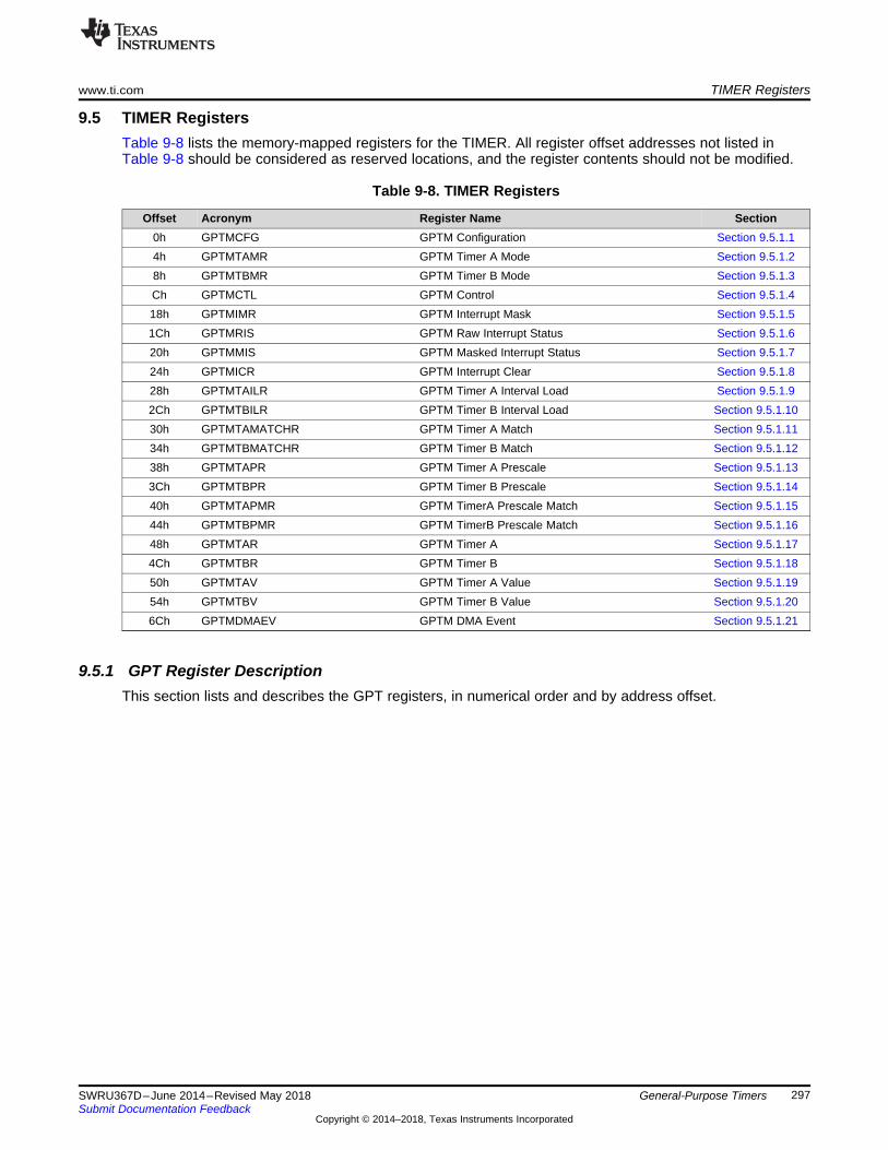
www.ti.com TIMER Registers
297SWRU367D–June 2014–Revised May 2018Submit Documentation Feedback
Copyright © 2014–2018, Texas Instruments Incorporated
General-Purpose Timers
9.5 TIMER RegistersTable 9-8 lists the memory-mapped registers for the TIMER. All register offset addresses not listed inTable 9-8 should be considered as reserved locations, and the register contents should not be modified.
Table 9-8. TIMER Registers
Offset Acronym Register Name Section0h GPTMCFG GPTM Configuration Section 9.5.1.14h GPTMTAMR GPTM Timer A Mode Section 9.5.1.28h GPTMTBMR GPTM Timer B Mode Section 9.5.1.3Ch GPTMCTL GPTM Control Section 9.5.1.418h GPTMIMR GPTM Interrupt Mask Section 9.5.1.51Ch GPTMRIS GPTM Raw Interrupt Status Section 9.5.1.620h GPTMMIS GPTM Masked Interrupt Status Section 9.5.1.724h GPTMICR GPTM Interrupt Clear Section 9.5.1.828h GPTMTAILR GPTM Timer A Interval Load Section 9.5.1.92Ch GPTMTBILR GPTM Timer B Interval Load Section 9.5.1.1030h GPTMTAMATCHR GPTM Timer A Match Section 9.5.1.1134h GPTMTBMATCHR GPTM Timer B Match Section 9.5.1.1238h GPTMTAPR GPTM Timer A Prescale Section 9.5.1.133Ch GPTMTBPR GPTM Timer B Prescale Section 9.5.1.1440h GPTMTAPMR GPTM TimerA Prescale Match Section 9.5.1.1544h GPTMTBPMR GPTM TimerB Prescale Match Section 9.5.1.1648h GPTMTAR GPTM Timer A Section 9.5.1.174Ch GPTMTBR GPTM Timer B Section 9.5.1.1850h GPTMTAV GPTM Timer A Value Section 9.5.1.1954h GPTMTBV GPTM Timer B Value Section 9.5.1.206Ch GPTMDMAEV GPTM DMA Event Section 9.5.1.21
9.5.1 GPT Register DescriptionThis section lists and describes the GPT registers, in numerical order and by address offset.
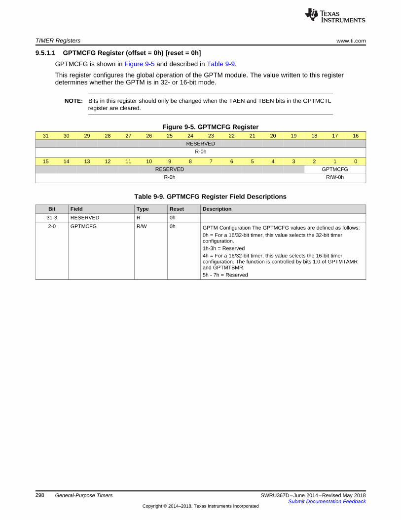
TIMER Registers www.ti.com
298 SWRU367D–June 2014–Revised May 2018Submit Documentation Feedback
Copyright © 2014–2018, Texas Instruments Incorporated
General-Purpose Timers
9.5.1.1 GPTMCFG Register (offset = 0h) [reset = 0h]GPTMCFG is shown in Figure 9-5 and described in Table 9-9.
This register configures the global operation of the GPTM module. The value written to this registerdetermines whether the GPTM is in 32- or 16-bit mode.
NOTE: Bits in this register should only be changed when the TAEN and TBEN bits in the GPTMCTLregister are cleared.
Figure 9-5. GPTMCFG Register31 30 29 28 27 26 25 24 23 22 21 20 19 18 17 16
RESERVEDR-0h
15 14 13 12 11 10 9 8 7 6 5 4 3 2 1 0RESERVED GPTMCFG
R-0h R/W-0h
Table 9-9. GPTMCFG Register Field Descriptions
Bit Field Type Reset Description31-3 RESERVED R 0h2-0 GPTMCFG R/W 0h GPTM Configuration The GPTMCFG values are defined as follows:
0h = For a 16/32-bit timer, this value selects the 32-bit timerconfiguration.1h-3h = Reserved4h = For a 16/32-bit timer, this value selects the 16-bit timerconfiguration. The function is controlled by bits 1:0 of GPTMTAMRand GPTMTBMR.5h - 7h = Reserved
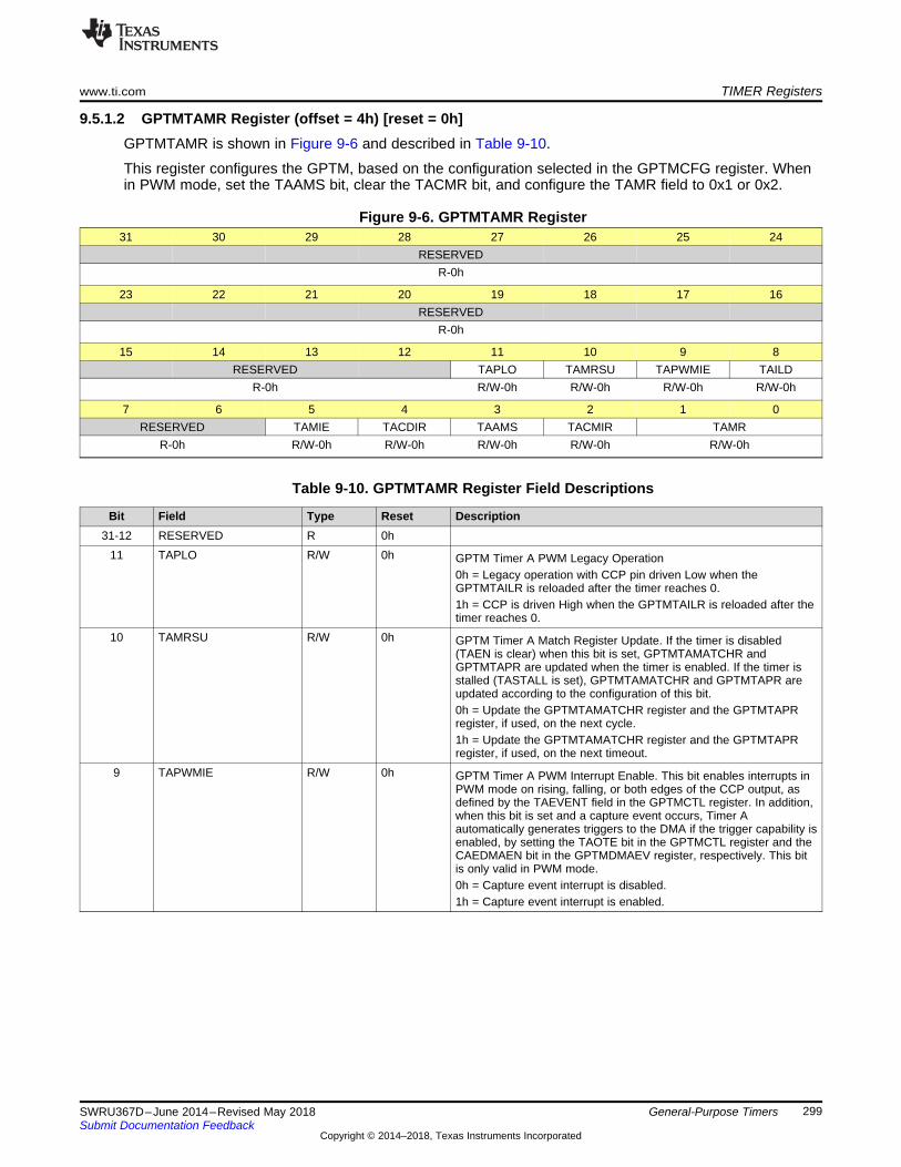
www.ti.com TIMER Registers
299SWRU367D–June 2014–Revised May 2018Submit Documentation Feedback
Copyright © 2014–2018, Texas Instruments Incorporated
General-Purpose Timers
9.5.1.2 GPTMTAMR Register (offset = 4h) [reset = 0h]GPTMTAMR is shown in Figure 9-6 and described in Table 9-10.
This register configures the GPTM, based on the configuration selected in the GPTMCFG register. Whenin PWM mode, set the TAAMS bit, clear the TACMR bit, and configure the TAMR field to 0x1 or 0x2.
Figure 9-6. GPTMTAMR Register31 30 29 28 27 26 25 24
RESERVEDR-0h
23 22 21 20 19 18 17 16RESERVED
R-0h
15 14 13 12 11 10 9 8RESERVED TAPLO TAMRSU TAPWMIE TAILD
R-0h R/W-0h R/W-0h R/W-0h R/W-0h
7 6 5 4 3 2 1 0RESERVED TAMIE TACDIR TAAMS TACMIR TAMR
R-0h R/W-0h R/W-0h R/W-0h R/W-0h R/W-0h
Table 9-10. GPTMTAMR Register Field Descriptions
Bit Field Type Reset Description31-12 RESERVED R 0h
11 TAPLO R/W 0h GPTM Timer A PWM Legacy Operation0h = Legacy operation with CCP pin driven Low when theGPTMTAILR is reloaded after the timer reaches 0.1h = CCP is driven High when the GPTMTAILR is reloaded after thetimer reaches 0.
10 TAMRSU R/W 0h GPTM Timer A Match Register Update. If the timer is disabled(TAEN is clear) when this bit is set, GPTMTAMATCHR andGPTMTAPR are updated when the timer is enabled. If the timer isstalled (TASTALL is set), GPTMTAMATCHR and GPTMTAPR areupdated according to the configuration of this bit.0h = Update the GPTMTAMATCHR register and the GPTMTAPRregister, if used, on the next cycle.1h = Update the GPTMTAMATCHR register and the GPTMTAPRregister, if used, on the next timeout.
9 TAPWMIE R/W 0h GPTM Timer A PWM Interrupt Enable. This bit enables interrupts inPWM mode on rising, falling, or both edges of the CCP output, asdefined by the TAEVENT field in the GPTMCTL register. In addition,when this bit is set and a capture event occurs, Timer Aautomatically generates triggers to the DMA if the trigger capability isenabled, by setting the TAOTE bit in the GPTMCTL register and theCAEDMAEN bit in the GPTMDMAEV register, respectively. This bitis only valid in PWM mode.0h = Capture event interrupt is disabled.1h = Capture event interrupt is enabled.
TIMER Registers www.ti.com
300 SWRU367D–June 2014–Revised May 2018Submit Documentation Feedback
Copyright © 2014–2018, Texas Instruments Incorporated
General-Purpose Timers
Table 9-10. GPTMTAMR Register Field Descriptions (continued)Bit Field Type Reset Description8 TAILD R/W 0h GPTM Timer A Interval Load Write. Note the state of this bit has no
effect when counting up. The bit descriptions above apply if the timeris enabled and running. If the timer is disabled (TAEN is clear) whenthis bit is set, GPTMTAR, GPTMTAV, and GPTMTAPs are updatedwhen the timer is enabled. If the timer is stalled (TASTALL is set),GPTMTAR and GPTMTAPS are updated according to theconfiguration of this bit.0h = Updates the GPTMTAR and GPTMTAV registers with the valuein the GPTMTAILR register on the next cycle. Also updates theGPTMTAPS register with the value in the GPTMTAPR register onthe next cycle.1h = Updates the GPTMTAR and GPTMTAV registers with the valuein the GPTMTAILR register on the next timeout. Also updates theGPTMTAPS register with the value in the GPTMTAPR register onthe next timeout.
7-6 RESERVED R 0h5 TAMIE R/W 0h GPTM Timer A Match Interrupt Enable
0h = The match interrupt is disabled for match events. Additionally,triggers to the DMA on match events are prevented.1h = An interrupt is generated when the match value in theGPTMTAMATCHR register is reached in the one-shot and periodicmodes.
4 TACDIR R/W 0h GPTM Timer A Count Direction. When in PWM mode, the status ofthis bit is ignored. PWM mode always counts down.0h = The timer counts down.1h = The timer counts up. When counting up, the timer starts from avalue of 0x0.
3 TAAMS R/W 0h GPTM Timer A Alternate Mode Select. The TAAMS values aredefined as follows. Note: To enable PWM mode, clear the TACMRbit and configure the TAMR field to 0x1 or 0x2.0h = Capture or compare mode is enabled.1h = PWM mode is enabled.
2 TACMIR R/W 0h GPTM Timer A Capture Mode. The TACMR values are defined asfollows:0h = Edge-count mode1h = Edge-time mode
1-0 TAMR R/W 0h GPTM Timer A Mode. The TAMR values are defined as follows: Thetimer mode is based on the timer configuration defined by bits 2:0 inthe GPTMCFG register.0h = Reserved1h = One-shot timer mode2h = Periodic timer mode3h = Capture mode
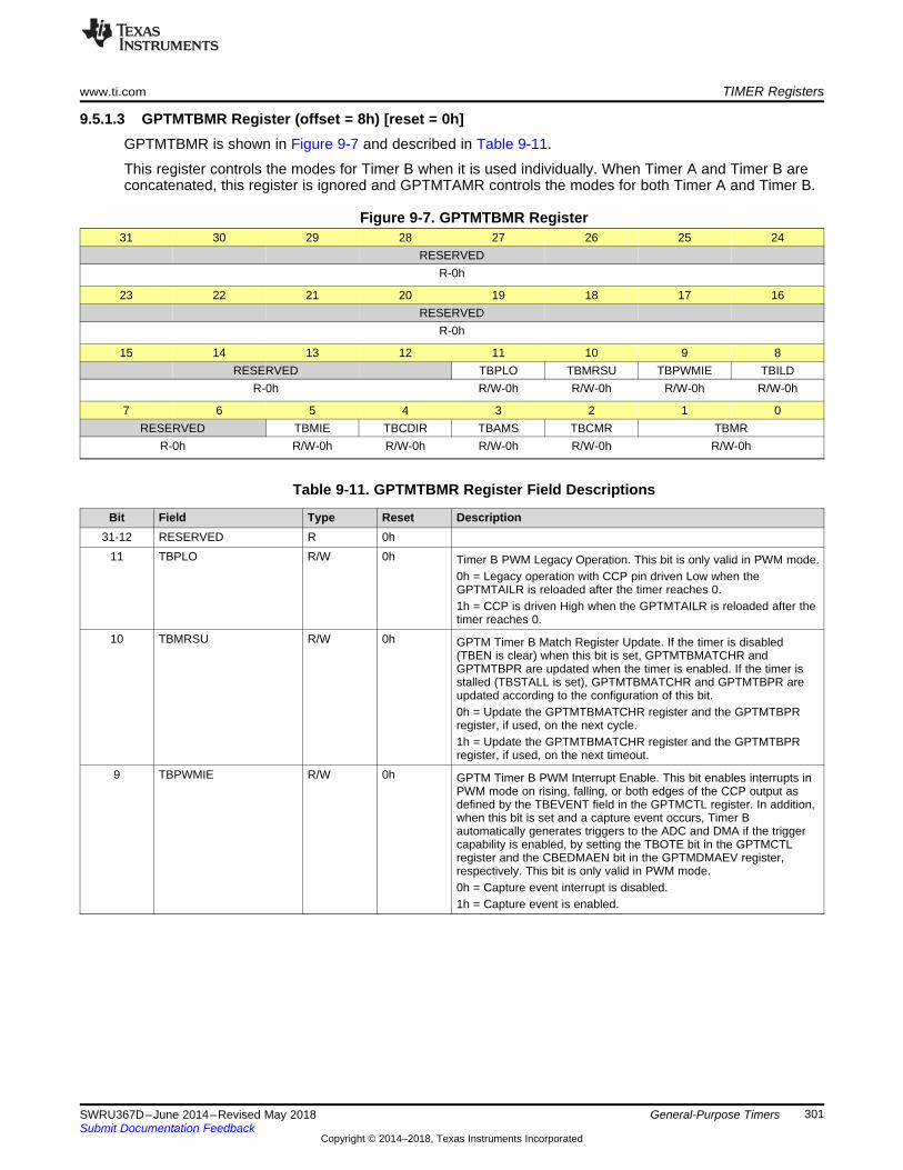
www.ti.com TIMER Registers
301SWRU367D–June 2014–Revised May 2018Submit Documentation Feedback
Copyright © 2014–2018, Texas Instruments Incorporated
General-Purpose Timers
9.5.1.3 GPTMTBMR Register (offset = 8h) [reset = 0h]GPTMTBMR is shown in Figure 9-7 and described in Table 9-11.
This register controls the modes for Timer B when it is used individually. When Timer A and Timer B areconcatenated, this register is ignored and GPTMTAMR controls the modes for both Timer A and Timer B.
Figure 9-7. GPTMTBMR Register31 30 29 28 27 26 25 24
RESERVEDR-0h
23 22 21 20 19 18 17 16RESERVED
R-0h
15 14 13 12 11 10 9 8RESERVED TBPLO TBMRSU TBPWMIE TBILD
R-0h R/W-0h R/W-0h R/W-0h R/W-0h
7 6 5 4 3 2 1 0RESERVED TBMIE TBCDIR TBAMS TBCMR TBMR
R-0h R/W-0h R/W-0h R/W-0h R/W-0h R/W-0h
Table 9-11. GPTMTBMR Register Field Descriptions
Bit Field Type Reset Description31-12 RESERVED R 0h
11 TBPLO R/W 0h Timer B PWM Legacy Operation. This bit is only valid in PWM mode.0h = Legacy operation with CCP pin driven Low when theGPTMTAILR is reloaded after the timer reaches 0.1h = CCP is driven High when the GPTMTAILR is reloaded after thetimer reaches 0.
10 TBMRSU R/W 0h GPTM Timer B Match Register Update. If the timer is disabled(TBEN is clear) when this bit is set, GPTMTBMATCHR andGPTMTBPR are updated when the timer is enabled. If the timer isstalled (TBSTALL is set), GPTMTBMATCHR and GPTMTBPR areupdated according to the configuration of this bit.0h = Update the GPTMTBMATCHR register and the GPTMTBPRregister, if used, on the next cycle.1h = Update the GPTMTBMATCHR register and the GPTMTBPRregister, if used, on the next timeout.
9 TBPWMIE R/W 0h GPTM Timer B PWM Interrupt Enable. This bit enables interrupts inPWM mode on rising, falling, or both edges of the CCP output asdefined by the TBEVENT field in the GPTMCTL register. In addition,when this bit is set and a capture event occurs, Timer Bautomatically generates triggers to the ADC and DMA if the triggercapability is enabled, by setting the TBOTE bit in the GPTMCTLregister and the CBEDMAEN bit in the GPTMDMAEV register,respectively. This bit is only valid in PWM mode.0h = Capture event interrupt is disabled.1h = Capture event is enabled.
TIMER Registers www.ti.com
302 SWRU367D–June 2014–Revised May 2018Submit Documentation Feedback
Copyright © 2014–2018, Texas Instruments Incorporated
General-Purpose Timers
Table 9-11. GPTMTBMR Register Field Descriptions (continued)Bit Field Type Reset Description8 TBILD R/W 0h GPTM Timer B Interval Load Write. The state of this bit has no effect
when counting up. The bit descriptions above apply if the timer isenabled and running. If the timer is disabled (TBEN is clear) whenthis bit is set, GPTMTBR, GPTMTBV, and GPTMTBPS are updatedwhen the timer is enabled. If the timer is stalled (TBSTALL is set),GPTMTBR and GPTMTBPS are updated according to theconfiguration of this bit.0h = Update the GPTMTBR and GPTMTBV registers with the valuein the GPTMTBILR register on the next cycle. Also update theGPTMTBPS register with the value in the GPTMTBPR register onthe next cycle.1h = Update the GPTMTBR and GPTMTBV registers with the valuein the GPTMTBILR register on the next timeout. Also update theGPTMTBPS register with the value in the GPTMTBPR register onthe next timeout.
7-6 RESERVED R 0h5 TBMIE R/W 0h GPTM Timer B Match Interrupt Enable
0h = The match interrupt is disabled for match events. Additionally,triggers to the DMA on match events are prevented.1h = An interrupt is generated when the match value in theGPTMTBMATCHR register is reached in the one-shot and periodicmodes.
4 TBCDIR R/W 0h GPTM Timer B Count Direction0h = The timer counts down.1h = The timer counts up. When counting up, the timer starts from avalue of 0x0. When in PWM mode, the status of this bit is ignored.PWM mode always counts down.
3 TBAMS R/W 0h GPTM Timer B Alternate Mode Select. The TBAMS values aredefined as follows. To enable PWM mode, clear the TBCMR bit andconfigure the TBMR field to 0x1 or 0x2.0h = Capture or compare mode is enabled.1h = PWM mode is enabled.
2 TBCMR R/W 0h GPTM Timer B Capture Mode. The TBCMR values are defined asfollows:0h = Edge-count mode1h = Edge-time mode
1-0 TBMR R/W 0h GPTM Timer B Mode. The TBMR values are defined as follows. Thetimer mode is based on the timer configuration defined by bits 2:0 inthe GPTMCFG register.0h = Reserved1h = One-shot timer mode2h = Periodic timer mode3h = Capture mode
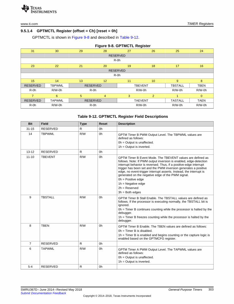
www.ti.com TIMER Registers
303SWRU367D–June 2014–Revised May 2018Submit Documentation Feedback
Copyright © 2014–2018, Texas Instruments Incorporated
General-Purpose Timers
9.5.1.4 GPTMCTL Register (offset = Ch) [reset = 0h]GPTMCTL is shown in Figure 9-8 and described in Table 9-12.
Figure 9-8. GPTMCTL Register31 30 29 28 27 26 25 24
RESERVEDR-0h
23 22 21 20 19 18 17 16RESERVED
R-0h
15 14 13 12 11 10 9 8RESERVED TBPWML RESERVED TBEVENT TBSTALL TBEN
R-0h R/W-0h R-0h R/W-0h R/W-0h R/W-0h
7 6 5 4 3 2 1 0RESERVED TAPWML RESERVED TAEVENT TASTALL TAEN
R-0h R/W-0h R-0h R/W-0h R/W-0h R/W-0h
Table 9-12. GPTMCTL Register Field Descriptions
Bit Field Type Reset Description31-15 RESERVED R 0h
14 TBPWML R/W 0h GPTM Timer B PWM Output Level. The TBPWML values aredefined as follows:0h = Output is unaffected.1h = Output is inverted.
13-12 RESERVED R 0h11-10 TBEVENT R/W 0h GPTM Timer B Event Mode. The TBEVENT values are defined as
follows. Note: If PWM output inversion is enabled, edge-detectioninterrupt behavior is reversed. Thus, if a positive-edge interrupttrigger has been set and the PWM inversion generates a positiveedge, no event-trigger interrupt asserts. Instead, the interrupt isgenerated on the negative edge of the PWM signal.0h = Positive edge1h = Negative edge2h = Reserved3h = Both edges
9 TBSTALL R/W 0h GPTM Timer B Stall Enable. The TBSTALL values are defined asfollows. If the processor is executing normally, the TBSTALL bit isignored.0h = Timer B continues counting while the processor is halted by thedebugger.1h = Timer B freezes counting while the processor is halted by thedebugger.
8 TBEN R/W 0h GPTM Timer B Enable. The TBEN values are defined as follows:0h = Timer B is disabled.1h = Timer B is enabled and begins counting or the capture logic isenabled based on the GPTMCFG register.
7 RESERVED R 0h6 TAPWML R/W 0h GPTM Timer A PWM Output Level. The TAPWML values are
defined as follows:0h = Output is unaffected.1h = Output is inverted.
5-4 RESERVED R 0h
TIMER Registers www.ti.com
304 SWRU367D–June 2014–Revised May 2018Submit Documentation Feedback
Copyright © 2014–2018, Texas Instruments Incorporated
General-Purpose Timers
Table 9-12. GPTMCTL Register Field Descriptions (continued)Bit Field Type Reset Description3-2 TAEVENT R/W 0h GPTM Timer A Event Mode. The TAEVENT values are defined as
follows. If PWM output inversion is enabled, edge-detection interruptbehavior is reversed. Thus, if a positive-edge interrupt trigger hasbeen set and the PWM inversion generates a positive edge, noevent-trigger interrupt asserts. Instead, the interrupt is generated onthe negative edge of the PWM signal.0h = Positive edge1h = Negative edge2h = Reserved3h = Both edges
1 TASTALL R/W 0h GPTM Timer A Stall Enable. The TASTALL values are defined asfollows. If the processor is executing normally, the TASTALL bit isignored.0h = Timer A continues counting while the processor is halted by thedebugger.1h = Timer A freezes counting while the processor is halted by thedebugger.
0 TAEN R/W 0h GPTM Timer A Enable. The TAEN values are defined as follows:0h = Timer A is disabled.1h = Timer A is enabled and begins counting or the capture logic isenabled based on the GPTMCFG register.
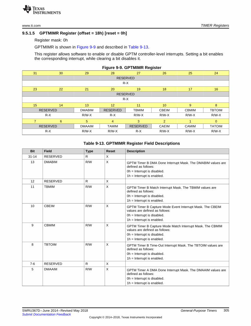
www.ti.com TIMER Registers
305SWRU367D–June 2014–Revised May 2018Submit Documentation Feedback
Copyright © 2014–2018, Texas Instruments Incorporated
General-Purpose Timers
9.5.1.5 GPTMIMR Register (offset = 18h) [reset = 0h]Register mask: 0h
GPTMIMR is shown in Figure 9-9 and described in Table 9-13.
This register allows software to enable or disable GPTM controller-level interrupts. Setting a bit enablesthe corresponding interrupt, while clearing a bit disables it.
Figure 9-9. GPTMIMR Register31 30 29 28 27 26 25 24
RESERVEDR-X
23 22 21 20 19 18 17 16RESERVED
R-X
15 14 13 12 11 10 9 8RESERVED DMABIM RESERVED TBMIM CBEIM CBMIM TBTOIM
R-X R/W-X R-X R/W-X R/W-X R/W-X R/W-X
7 6 5 4 3 2 1 0RESERVED DMAAIM TAMIM RESERVED CAEIM CAMIM TATOIM
R-X R/W-X R/W-X R-X R/W-X R/W-X R/W-X
Table 9-13. GPTMIMR Register Field Descriptions
Bit Field Type Reset Description31-14 RESERVED R X
13 DMABIM R/W X GPTM Timer B DMA Done Interrupt Mask. The DMABIM values aredefined as follows:0h = Interrupt is disabled.1h = Interrupt is enabled.
12 RESERVED R X11 TBMIM R/W X GPTM Timer B Match Interrupt Mask. The TBMIM values are
defined as follows:0h = Interrupt is disabled.1h = Interrupt is enabled.
10 CBEIM R/W X GPTM Timer B Capture Mode Event Interrupt Mask. The CBEIMvalues are defined as follows:0h = Interrupt is disabled.1h = Interrupt is enabled.
9 CBMIM R/W X GPTM Timer B Capture Mode Match Interrupt Mask. The CBMIMvalues are defined as follows:0h = Interrupt is disabled.1h = Interrupt is enabled.
8 TBTOIM R/W X GPTM Timer B Time-Out Interrupt Mask. The TBTOIM values aredefined as follows:0h = Interrupt is disabled.1h = Interrupt is enabled.
7-6 RESERVED R X5 DMAAIM R/W X GPTM Timer A DMA Done Interrupt Mask. The DMAAIM values are
defined as follows:0h = Interrupt is disabled.1h = Interrupt is enabled.
TIMER Registers www.ti.com
306 SWRU367D–June 2014–Revised May 2018Submit Documentation Feedback
Copyright © 2014–2018, Texas Instruments Incorporated
General-Purpose Timers
Table 9-13. GPTMIMR Register Field Descriptions (continued)Bit Field Type Reset Description4 TAMIM R/W X GPTM Timer A Match Interrupt Mask. The TAMIM values are
defined as follows:0h = Interrupt is disabled.1h = Interrupt is enabled.
3 RESERVED R X2 CAEIM R/W X GPTM Timer A Capture Mode Event Interrupt Mask. The CAEIM
values are defined as follows:0h = Interrupt is disabled.1h = Interrupt is enabled.
1 CAMIM R/W X GPTM Timer A Capture Mode Match Interrupt Mask. The CAMIMvalues are defined as follows:0h = Interrupt is disabled.1h = Interrupt is enabled.
0 TATOIM R/W X GPTM Timer A Time-Out Interrupt Mask. The TATOIM values aredefined as follows:0h = Interrupt is disabled.1h = Interrupt is enabled.
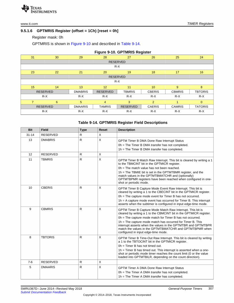
www.ti.com TIMER Registers
307SWRU367D–June 2014–Revised May 2018Submit Documentation Feedback
Copyright © 2014–2018, Texas Instruments Incorporated
General-Purpose Timers
9.5.1.6 GPTMRIS Register (offset = 1Ch) [reset = 0h]Register mask: 0h
GPTMRIS is shown in Figure 9-10 and described in Table 9-14.
Figure 9-10. GPTMRIS Register31 30 29 28 27 26 25 24
RESERVEDR-X
23 22 21 20 19 18 17 16RESERVED
R-X
15 14 13 12 11 10 9 8RESERVED DMABRIS RESERVED TBMRIS CBERIS CBMRIS TBTORIS
R-X R-X R-X R-X R-X R-X R-X
7 6 5 4 3 2 1 0RESERVED DMAARIS TAMRIS RESERVED CAERIS CAMRIS TATORIS
R-X R-X R-X R-X R-X R-X R-X
Table 9-14. GPTMRIS Register Field Descriptions
Bit Field Type Reset Description31-14 RESERVED R X
13 DMABRIS R X GPTM Timer B DMA Done Raw Interrupt Status0h = The Timer B DMA transfer has not completed.1h = The Timer B DMA transfer has completed.
12 RESERVED R X11 TBMRIS R X GPTM Timer B Match Raw Interrupt. This bit is cleared by writing a 1
to the TBMCINT bit in the GPTMICR register.0h = The match value has not been reached.1h = The TBMIE bit is set in the GPTMTBMR register, and thematch values in the GPTMTBMATCHR and (optionally)GPTMTBPMR registers have been reached when configured in one-shot or periodic mode.
10 CBERIS R X GPTM Timer B Capture Mode Event Raw Interrupt. This bit iscleared by writing a 1 to the CBECINT bit in the GPTMICR register.0h = The capture mode event for Timer B has not occurred.1h = A capture mode event has occurred for Timer B. This interruptasserts when the subtimer is configured in input edge-time mode.
9 CBMRIS R X GPTM Timer B Capture Mode Match Raw Interrupt. This bit iscleared by writing a 1 to the CBMCINT bit in the GPTMICR register.0h = The capture mode match for Timer B has not occurred.1h = The capture mode match has occurred for Timer B. Thisinterrupt asserts when the values in the GPTMTBR and GPTMTBPRmatch the values in the GPTMTBMATCHR and GPTMTBPMR whenconfigured in input edge-time mode.
8 TBTORIS R X GPTM Timer B Time-Out Raw Interrupt. This bit is cleared by writinga 1 to the TBTOCINT bit in the GPTMICR register.0h = Timer B has not timed out.1h = Timer B has timed out. This interrupt is asserted when a one-shot or periodic mode timer reaches the count limit (0 or the valueloaded into GPTMTBILR, depending on the count direction).
7-6 RESERVED R X5 DMAARIS R X GPTM Timer A DMA Done Raw Interrupt Status
0h = The Timer A DMA transfer has not completed.1h = The Timer A DMA transfer has completed.
TIMER Registers www.ti.com
308 SWRU367D–June 2014–Revised May 2018Submit Documentation Feedback
Copyright © 2014–2018, Texas Instruments Incorporated
General-Purpose Timers
Table 9-14. GPTMRIS Register Field Descriptions (continued)Bit Field Type Reset Description4 TAMRIS R X GPTM Timer A Match Raw Interrupt. This bit is cleared by writing a 1
to the TAMCINT bit in the GPTMICR register.0h = The match value has not been reached.1h = The TAMIE bit is set in the GPTMTAMR register, and thematch value in the GPTMTAMATCHR and (optionally)GPTMTAPMR registers have been reached when configured in one-shot or periodic mode.
3 RESERVED R X2 CAERIS R X GPTM Timer A Capture Mode Event Raw Interrupt. This bit is
cleared by writing a 1 to the CAECINT bit in the GPTMICR register.0h = The capture mode event for Timer A has not occurred.1h = A capture mode event has occurred for Timer A. This interruptasserts when the subtimer is configured in input edge-time mode.
1 CAMRIS R X GPTM Timer A Capture Mode Match Raw Interrupt. This bit iscleared by writing a 1 to the CAMCINT bit in the GPTMICR register.0h = The capture mode match for Timer A has not occurred.1h = A capture mode match has occurred for Timer A. This interruptasserts when the values in the GPTMTAR and GPTMTAPR matchthe values in the GPTMTAMATCHR and GPTMTAPMR whenconfigured in input edge-time mode.
0 TATORIS R X GPTM Timer A Time-Out Raw Interrupt. This bit is cleared by writinga 1 to the TATOCINT bit in the GPTMICR register.0h = Timer A has not timed out.1h = Timer A has timed out. This interrupt is asserted when a one-shot or periodic mode timer reaches it's count limit (0 or the valueloaded into GPTMTAILR, depending on the count direction).
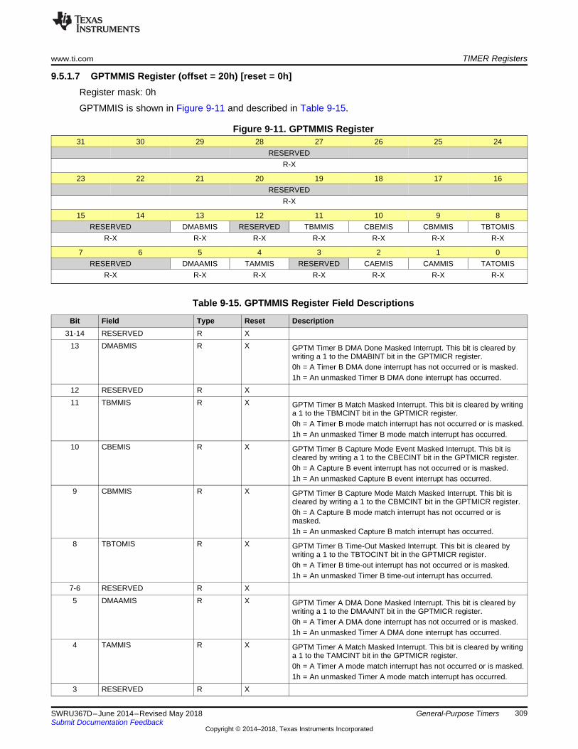
www.ti.com TIMER Registers
309SWRU367D–June 2014–Revised May 2018Submit Documentation Feedback
Copyright © 2014–2018, Texas Instruments Incorporated
General-Purpose Timers
9.5.1.7 GPTMMIS Register (offset = 20h) [reset = 0h]Register mask: 0h
GPTMMIS is shown in Figure 9-11 and described in Table 9-15.
Figure 9-11. GPTMMIS Register31 30 29 28 27 26 25 24
RESERVEDR-X
23 22 21 20 19 18 17 16RESERVED
R-X
15 14 13 12 11 10 9 8RESERVED DMABMIS RESERVED TBMMIS CBEMIS CBMMIS TBTOMIS
R-X R-X R-X R-X R-X R-X R-X
7 6 5 4 3 2 1 0RESERVED DMAAMIS TAMMIS RESERVED CAEMIS CAMMIS TATOMIS
R-X R-X R-X R-X R-X R-X R-X
Table 9-15. GPTMMIS Register Field Descriptions
Bit Field Type Reset Description31-14 RESERVED R X
13 DMABMIS R X GPTM Timer B DMA Done Masked Interrupt. This bit is cleared bywriting a 1 to the DMABINT bit in the GPTMICR register.0h = A Timer B DMA done interrupt has not occurred or is masked.1h = An unmasked Timer B DMA done interrupt has occurred.
12 RESERVED R X11 TBMMIS R X GPTM Timer B Match Masked Interrupt. This bit is cleared by writing
a 1 to the TBMCINT bit in the GPTMICR register.0h = A Timer B mode match interrupt has not occurred or is masked.1h = An unmasked Timer B mode match interrupt has occurred.
10 CBEMIS R X GPTM Timer B Capture Mode Event Masked Interrupt. This bit iscleared by writing a 1 to the CBECINT bit in the GPTMICR register.0h = A Capture B event interrupt has not occurred or is masked.1h = An unmasked Capture B event interrupt has occurred.
9 CBMMIS R X GPTM Timer B Capture Mode Match Masked Interrupt. This bit iscleared by writing a 1 to the CBMCINT bit in the GPTMICR register.0h = A Capture B mode match interrupt has not occurred or ismasked.1h = An unmasked Capture B match interrupt has occurred.
8 TBTOMIS R X GPTM Timer B Time-Out Masked Interrupt. This bit is cleared bywriting a 1 to the TBTOCINT bit in the GPTMICR register.0h = A Timer B time-out interrupt has not occurred or is masked.1h = An unmasked Timer B time-out interrupt has occurred.
7-6 RESERVED R X5 DMAAMIS R X GPTM Timer A DMA Done Masked Interrupt. This bit is cleared by
writing a 1 to the DMAAINT bit in the GPTMICR register.0h = A Timer A DMA done interrupt has not occurred or is masked.1h = An unmasked Timer A DMA done interrupt has occurred.
4 TAMMIS R X GPTM Timer A Match Masked Interrupt. This bit is cleared by writinga 1 to the TAMCINT bit in the GPTMICR register.0h = A Timer A mode match interrupt has not occurred or is masked.1h = An unmasked Timer A mode match interrupt has occurred.
3 RESERVED R X
TIMER Registers www.ti.com
310 SWRU367D–June 2014–Revised May 2018Submit Documentation Feedback
Copyright © 2014–2018, Texas Instruments Incorporated
General-Purpose Timers
Table 9-15. GPTMMIS Register Field Descriptions (continued)Bit Field Type Reset Description2 CAEMIS R X GPTM Timer A Capture Mode Event Masked Interrupt. This bit is
cleared by writing a 1 to the CAECINT bit in the GPTMICR register.0h = A Capture A event interrupt has not occurred or is masked.1h = An unmasked Capture A event interrupt has occurred.
1 CAMMIS R X GPTM Timer A Capture Mode Match Masked Interrupt. This bit iscleared by writing a 1 to the CAMCINT bit in the GPTMICR register.0h = A Capture A mode match interrupt has not occurred or ismasked.1h = An unmasked Capture A match interrupt has occurred.
0 TATOMIS R X GPTM Timer A Time-Out Masked Interrupt. This bit is cleared bywriting a 1 to the TATOCINT bit in the GPTMICR register.0h = A Timer A time-out interrupt has not occurred or is masked.1h = An unmasked Timer A time-out interrupt has occurred.
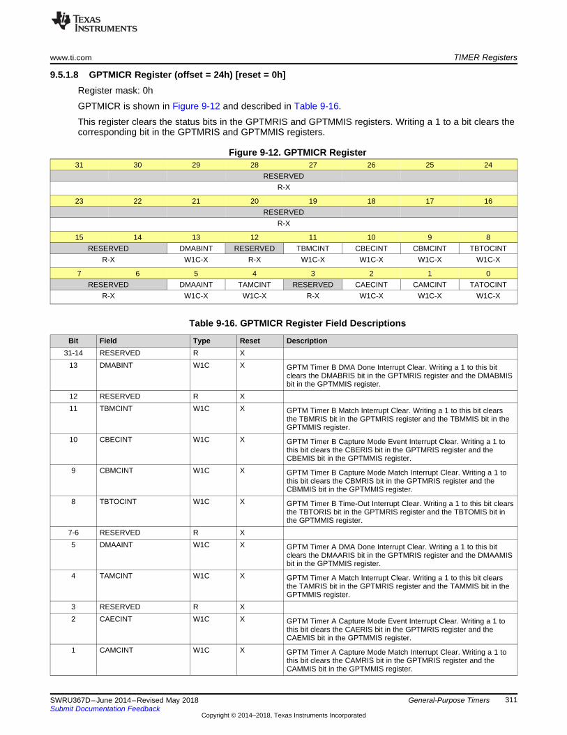
www.ti.com TIMER Registers
311SWRU367D–June 2014–Revised May 2018Submit Documentation Feedback
Copyright © 2014–2018, Texas Instruments Incorporated
General-Purpose Timers
9.5.1.8 GPTMICR Register (offset = 24h) [reset = 0h]Register mask: 0h
GPTMICR is shown in Figure 9-12 and described in Table 9-16.
This register clears the status bits in the GPTMRIS and GPTMMIS registers. Writing a 1 to a bit clears thecorresponding bit in the GPTMRIS and GPTMMIS registers.
Figure 9-12. GPTMICR Register31 30 29 28 27 26 25 24
RESERVEDR-X
23 22 21 20 19 18 17 16RESERVED
R-X
15 14 13 12 11 10 9 8RESERVED DMABINT RESERVED TBMCINT CBECINT CBMCINT TBTOCINT
R-X W1C-X R-X W1C-X W1C-X W1C-X W1C-X
7 6 5 4 3 2 1 0RESERVED DMAAINT TAMCINT RESERVED CAECINT CAMCINT TATOCINT
R-X W1C-X W1C-X R-X W1C-X W1C-X W1C-X
Table 9-16. GPTMICR Register Field Descriptions
Bit Field Type Reset Description31-14 RESERVED R X
13 DMABINT W1C X GPTM Timer B DMA Done Interrupt Clear. Writing a 1 to this bitclears the DMABRIS bit in the GPTMRIS register and the DMABMISbit in the GPTMMIS register.
12 RESERVED R X11 TBMCINT W1C X GPTM Timer B Match Interrupt Clear. Writing a 1 to this bit clears
the TBMRIS bit in the GPTMRIS register and the TBMMIS bit in theGPTMMIS register.
10 CBECINT W1C X GPTM Timer B Capture Mode Event Interrupt Clear. Writing a 1 tothis bit clears the CBERIS bit in the GPTMRIS register and theCBEMIS bit in the GPTMMIS register.
9 CBMCINT W1C X GPTM Timer B Capture Mode Match Interrupt Clear. Writing a 1 tothis bit clears the CBMRIS bit in the GPTMRIS register and theCBMMIS bit in the GPTMMIS register.
8 TBTOCINT W1C X GPTM Timer B Time-Out Interrupt Clear. Writing a 1 to this bit clearsthe TBTORIS bit in the GPTMRIS register and the TBTOMIS bit inthe GPTMMIS register.
7-6 RESERVED R X5 DMAAINT W1C X GPTM Timer A DMA Done Interrupt Clear. Writing a 1 to this bit
clears the DMAARIS bit in the GPTMRIS register and the DMAAMISbit in the GPTMMIS register.
4 TAMCINT W1C X GPTM Timer A Match Interrupt Clear. Writing a 1 to this bit clearsthe TAMRIS bit in the GPTMRIS register and the TAMMIS bit in theGPTMMIS register.
3 RESERVED R X2 CAECINT W1C X GPTM Timer A Capture Mode Event Interrupt Clear. Writing a 1 to
this bit clears the CAERIS bit in the GPTMRIS register and theCAEMIS bit in the GPTMMIS register.
1 CAMCINT W1C X GPTM Timer A Capture Mode Match Interrupt Clear. Writing a 1 tothis bit clears the CAMRIS bit in the GPTMRIS register and theCAMMIS bit in the GPTMMIS register.
TIMER Registers www.ti.com
312 SWRU367D–June 2014–Revised May 2018Submit Documentation Feedback
Copyright © 2014–2018, Texas Instruments Incorporated
General-Purpose Timers
Table 9-16. GPTMICR Register Field Descriptions (continued)Bit Field Type Reset Description0 TATOCINT W1C X GPTM Timer A Time-Out Raw Interrupt. Writing a 1 to this bit clears
the TATORIS bit in the GPTMRIS register and the TATOMIS bit inthe GPTMMIS register.
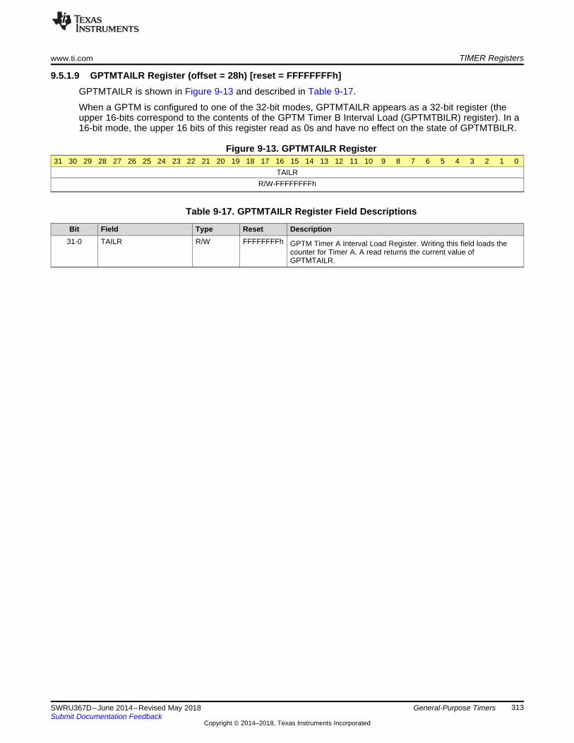
www.ti.com TIMER Registers
313SWRU367D–June 2014–Revised May 2018Submit Documentation Feedback
Copyright © 2014–2018, Texas Instruments Incorporated
General-Purpose Timers
9.5.1.9 GPTMTAILR Register (offset = 28h) [reset = FFFFFFFFh]GPTMTAILR is shown in Figure 9-13 and described in Table 9-17.
When a GPTM is configured to one of the 32-bit modes, GPTMTAILR appears as a 32-bit register (theupper 16-bits correspond to the contents of the GPTM Timer B Interval Load (GPTMTBILR) register). In a16-bit mode, the upper 16 bits of this register read as 0s and have no effect on the state of GPTMTBILR.
Figure 9-13. GPTMTAILR Register31 30 29 28 27 26 25 24 23 22 21 20 19 18 17 16 15 14 13 12 11 10 9 8 7 6 5 4 3 2 1 0
TAILRR/W-FFFFFFFFh
Table 9-17. GPTMTAILR Register Field Descriptions
Bit Field Type Reset Description31-0 TAILR R/W FFFFFFFFh GPTM Timer A Interval Load Register. Writing this field loads the
counter for Timer A. A read returns the current value ofGPTMTAILR.
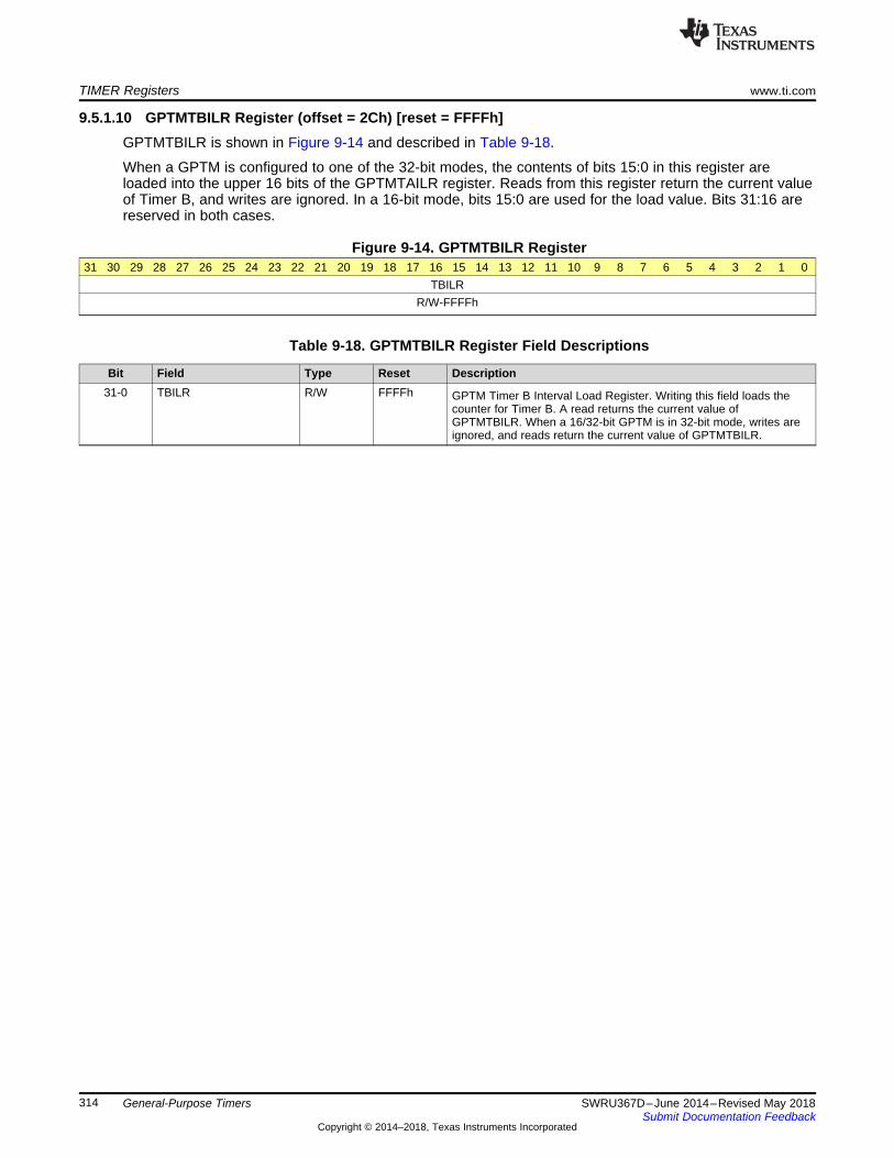
TIMER Registers www.ti.com
314 SWRU367D–June 2014–Revised May 2018Submit Documentation Feedback
Copyright © 2014–2018, Texas Instruments Incorporated
General-Purpose Timers
9.5.1.10 GPTMTBILR Register (offset = 2Ch) [reset = FFFFh]GPTMTBILR is shown in Figure 9-14 and described in Table 9-18.
When a GPTM is configured to one of the 32-bit modes, the contents of bits 15:0 in this register areloaded into the upper 16 bits of the GPTMTAILR register. Reads from this register return the current valueof Timer B, and writes are ignored. In a 16-bit mode, bits 15:0 are used for the load value. Bits 31:16 arereserved in both cases.
Figure 9-14. GPTMTBILR Register31 30 29 28 27 26 25 24 23 22 21 20 19 18 17 16 15 14 13 12 11 10 9 8 7 6 5 4 3 2 1 0
TBILRR/W-FFFFh
Table 9-18. GPTMTBILR Register Field Descriptions
Bit Field Type Reset Description31-0 TBILR R/W FFFFh GPTM Timer B Interval Load Register. Writing this field loads the
counter for Timer B. A read returns the current value ofGPTMTBILR. When a 16/32-bit GPTM is in 32-bit mode, writes areignored, and reads return the current value of GPTMTBILR.
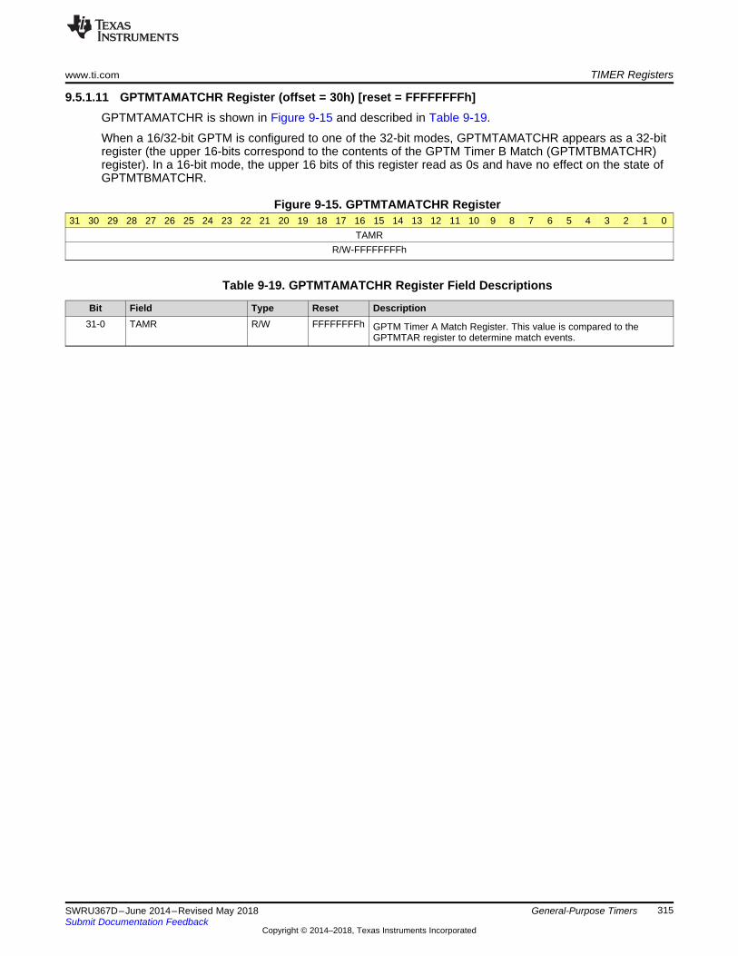
www.ti.com TIMER Registers
315SWRU367D–June 2014–Revised May 2018Submit Documentation Feedback
Copyright © 2014–2018, Texas Instruments Incorporated
General-Purpose Timers
9.5.1.11 GPTMTAMATCHR Register (offset = 30h) [reset = FFFFFFFFh]GPTMTAMATCHR is shown in Figure 9-15 and described in Table 9-19.
When a 16/32-bit GPTM is configured to one of the 32-bit modes, GPTMTAMATCHR appears as a 32-bitregister (the upper 16-bits correspond to the contents of the GPTM Timer B Match (GPTMTBMATCHR)register). In a 16-bit mode, the upper 16 bits of this register read as 0s and have no effect on the state ofGPTMTBMATCHR.
Figure 9-15. GPTMTAMATCHR Register31 30 29 28 27 26 25 24 23 22 21 20 19 18 17 16 15 14 13 12 11 10 9 8 7 6 5 4 3 2 1 0
TAMRR/W-FFFFFFFFh
Table 9-19. GPTMTAMATCHR Register Field Descriptions
Bit Field Type Reset Description31-0 TAMR R/W FFFFFFFFh GPTM Timer A Match Register. This value is compared to the
GPTMTAR register to determine match events.
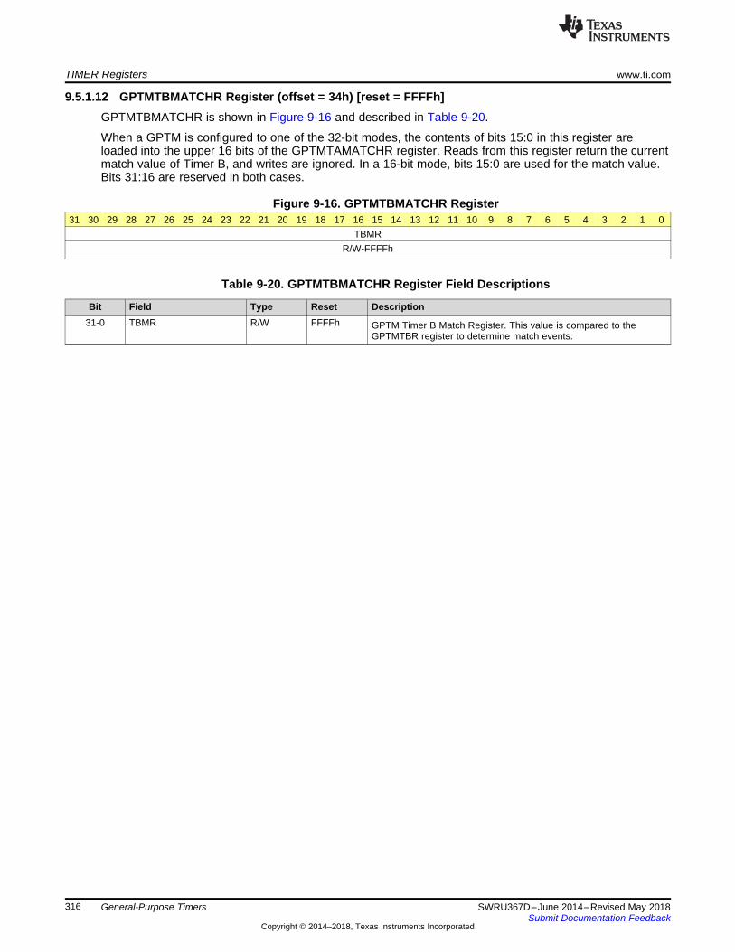
TIMER Registers www.ti.com
316 SWRU367D–June 2014–Revised May 2018Submit Documentation Feedback
Copyright © 2014–2018, Texas Instruments Incorporated
General-Purpose Timers
9.5.1.12 GPTMTBMATCHR Register (offset = 34h) [reset = FFFFh]GPTMTBMATCHR is shown in Figure 9-16 and described in Table 9-20.
When a GPTM is configured to one of the 32-bit modes, the contents of bits 15:0 in this register areloaded into the upper 16 bits of the GPTMTAMATCHR register. Reads from this register return the currentmatch value of Timer B, and writes are ignored. In a 16-bit mode, bits 15:0 are used for the match value.Bits 31:16 are reserved in both cases.
Figure 9-16. GPTMTBMATCHR Register31 30 29 28 27 26 25 24 23 22 21 20 19 18 17 16 15 14 13 12 11 10 9 8 7 6 5 4 3 2 1 0
TBMRR/W-FFFFh
Table 9-20. GPTMTBMATCHR Register Field Descriptions
Bit Field Type Reset Description31-0 TBMR R/W FFFFh GPTM Timer B Match Register. This value is compared to the
GPTMTBR register to determine match events.
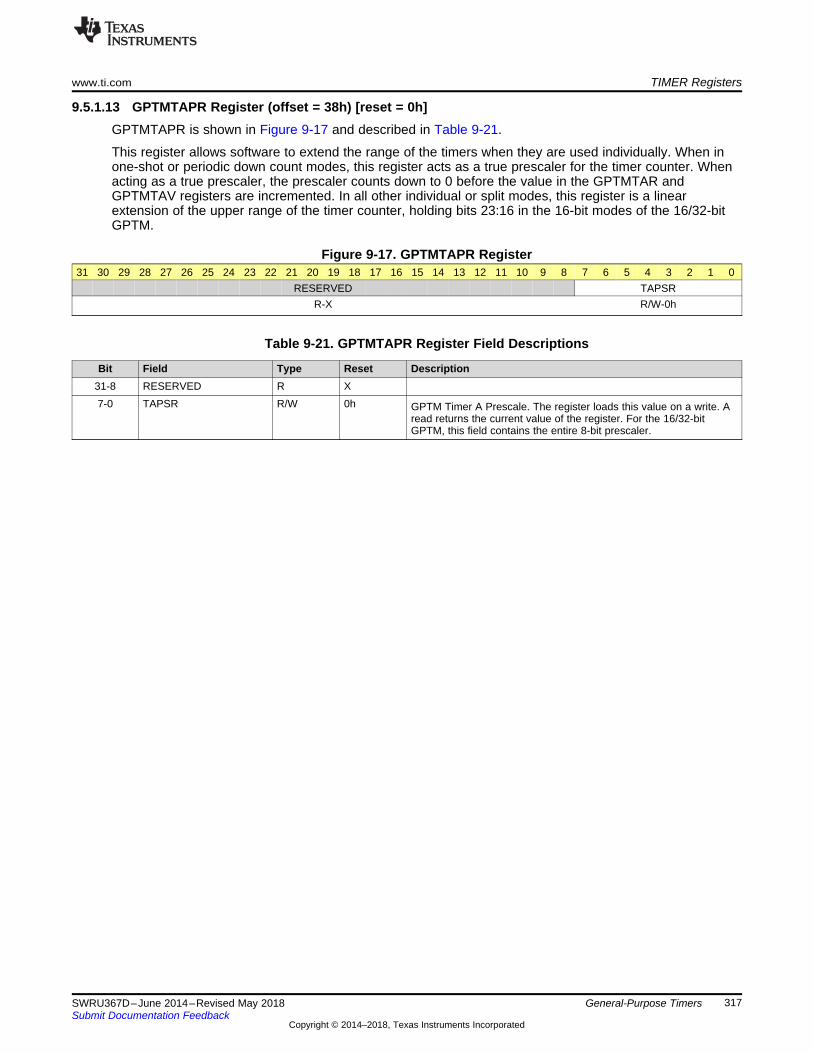
www.ti.com TIMER Registers
317SWRU367D–June 2014–Revised May 2018Submit Documentation Feedback
Copyright © 2014–2018, Texas Instruments Incorporated
General-Purpose Timers
9.5.1.13 GPTMTAPR Register (offset = 38h) [reset = 0h]GPTMTAPR is shown in Figure 9-17 and described in Table 9-21.
This register allows software to extend the range of the timers when they are used individually. When inone-shot or periodic down count modes, this register acts as a true prescaler for the timer counter. Whenacting as a true prescaler, the prescaler counts down to 0 before the value in the GPTMTAR andGPTMTAV registers are incremented. In all other individual or split modes, this register is a linearextension of the upper range of the timer counter, holding bits 23:16 in the 16-bit modes of the 16/32-bitGPTM.
Figure 9-17. GPTMTAPR Register31 30 29 28 27 26 25 24 23 22 21 20 19 18 17 16 15 14 13 12 11 10 9 8 7 6 5 4 3 2 1 0
RESERVED TAPSRR-X R/W-0h
Table 9-21. GPTMTAPR Register Field Descriptions
Bit Field Type Reset Description31-8 RESERVED R X7-0 TAPSR R/W 0h GPTM Timer A Prescale. The register loads this value on a write. A
read returns the current value of the register. For the 16/32-bitGPTM, this field contains the entire 8-bit prescaler.

TIMER Registers www.ti.com
318 SWRU367D–June 2014–Revised May 2018Submit Documentation Feedback
Copyright © 2014–2018, Texas Instruments Incorporated
General-Purpose Timers
9.5.1.14 GPTMTBPR Register (offset = 3Ch) [reset = 0h]GPTMTBPR is shown in Figure 9-18 and described in Table 9-22.
This register allows software to extend the range of the timers when they are used individually. When inone-shot or periodic down count modes, this register acts as a true prescaler for the timer counter. Whenacting as a true prescaler, the prescaler counts down to 0 before the value in the GPTMTBR and bregisters are incremented. In all other individual or split modes, this register is a linear extension of theupper range of the timer counter, holding bits 23:16 in the 16-bit modes of the 16/32-bit GPTM.
Figure 9-18. GPTMTBPR Register31 30 29 28 27 26 25 24 23 22 21 20 19 18 17 16 15 14 13 12 11 10 9 8 7 6 5 4 3 2 1 0
RESERVED TBPSRR-X R/W-0h
Table 9-22. GPTMTBPR Register Field Descriptions
Bit Field Type Reset Description31-8 RESERVED R X7-0 TBPSR R/W 0h GPTM Timer B Prescale. The register loads this value on a write. A
read returns the current value of this register. For the 16/32-bitGPTM, this field contains the entire 8-bit prescaler.
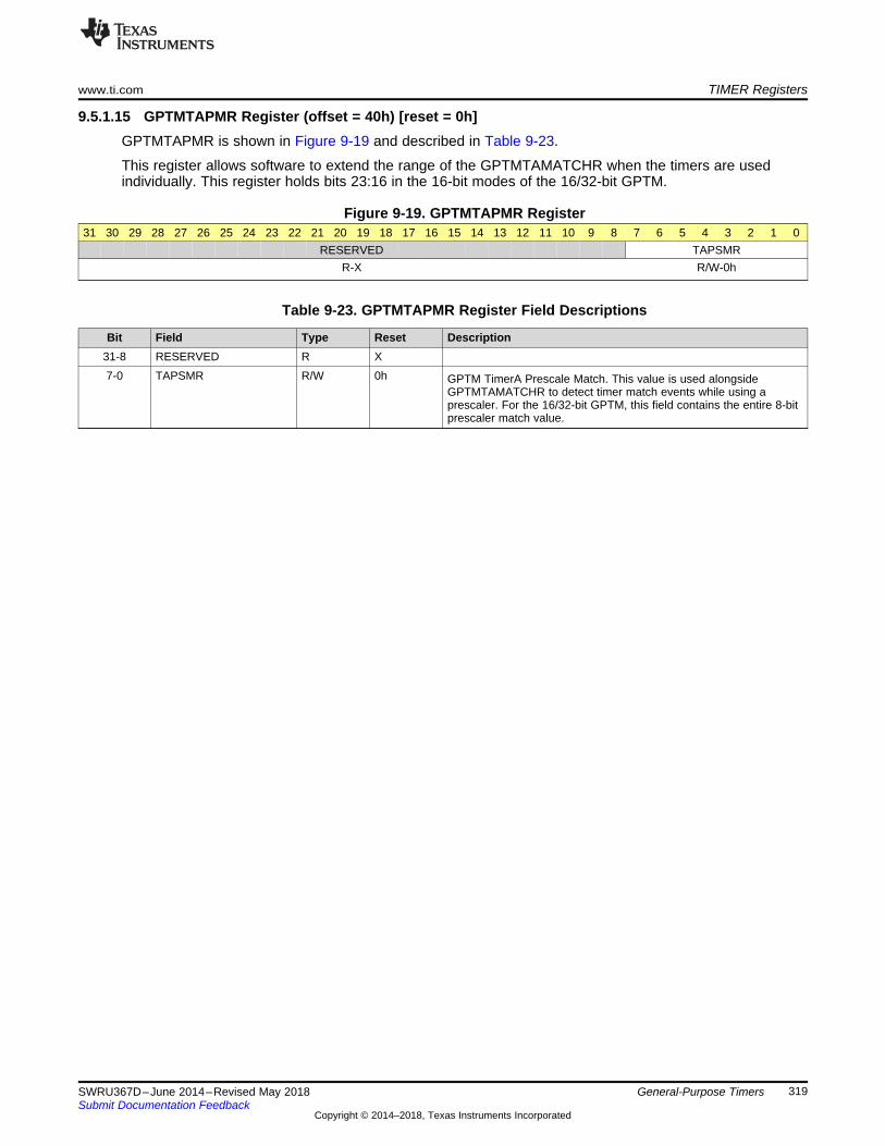
www.ti.com TIMER Registers
319SWRU367D–June 2014–Revised May 2018Submit Documentation Feedback
Copyright © 2014–2018, Texas Instruments Incorporated
General-Purpose Timers
9.5.1.15 GPTMTAPMR Register (offset = 40h) [reset = 0h]GPTMTAPMR is shown in Figure 9-19 and described in Table 9-23.
This register allows software to extend the range of the GPTMTAMATCHR when the timers are usedindividually. This register holds bits 23:16 in the 16-bit modes of the 16/32-bit GPTM.
Figure 9-19. GPTMTAPMR Register31 30 29 28 27 26 25 24 23 22 21 20 19 18 17 16 15 14 13 12 11 10 9 8 7 6 5 4 3 2 1 0
RESERVED TAPSMRR-X R/W-0h
Table 9-23. GPTMTAPMR Register Field Descriptions
Bit Field Type Reset Description31-8 RESERVED R X7-0 TAPSMR R/W 0h GPTM TimerA Prescale Match. This value is used alongside
GPTMTAMATCHR to detect timer match events while using aprescaler. For the 16/32-bit GPTM, this field contains the entire 8-bitprescaler match value.
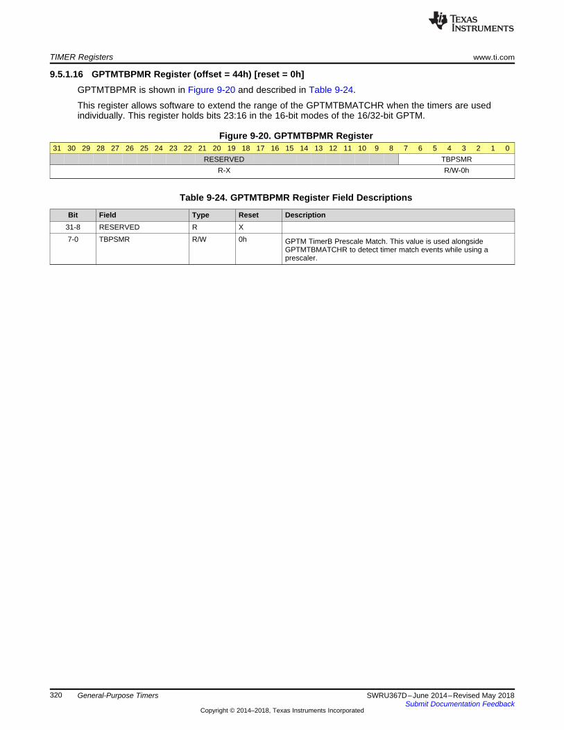
TIMER Registers www.ti.com
320 SWRU367D–June 2014–Revised May 2018Submit Documentation Feedback
Copyright © 2014–2018, Texas Instruments Incorporated
General-Purpose Timers
9.5.1.16 GPTMTBPMR Register (offset = 44h) [reset = 0h]GPTMTBPMR is shown in Figure 9-20 and described in Table 9-24.
This register allows software to extend the range of the GPTMTBMATCHR when the timers are usedindividually. This register holds bits 23:16 in the 16-bit modes of the 16/32-bit GPTM.
Figure 9-20. GPTMTBPMR Register31 30 29 28 27 26 25 24 23 22 21 20 19 18 17 16 15 14 13 12 11 10 9 8 7 6 5 4 3 2 1 0
RESERVED TBPSMRR-X R/W-0h
Table 9-24. GPTMTBPMR Register Field Descriptions
Bit Field Type Reset Description31-8 RESERVED R X7-0 TBPSMR R/W 0h GPTM TimerB Prescale Match. This value is used alongside
GPTMTBMATCHR to detect timer match events while using aprescaler.
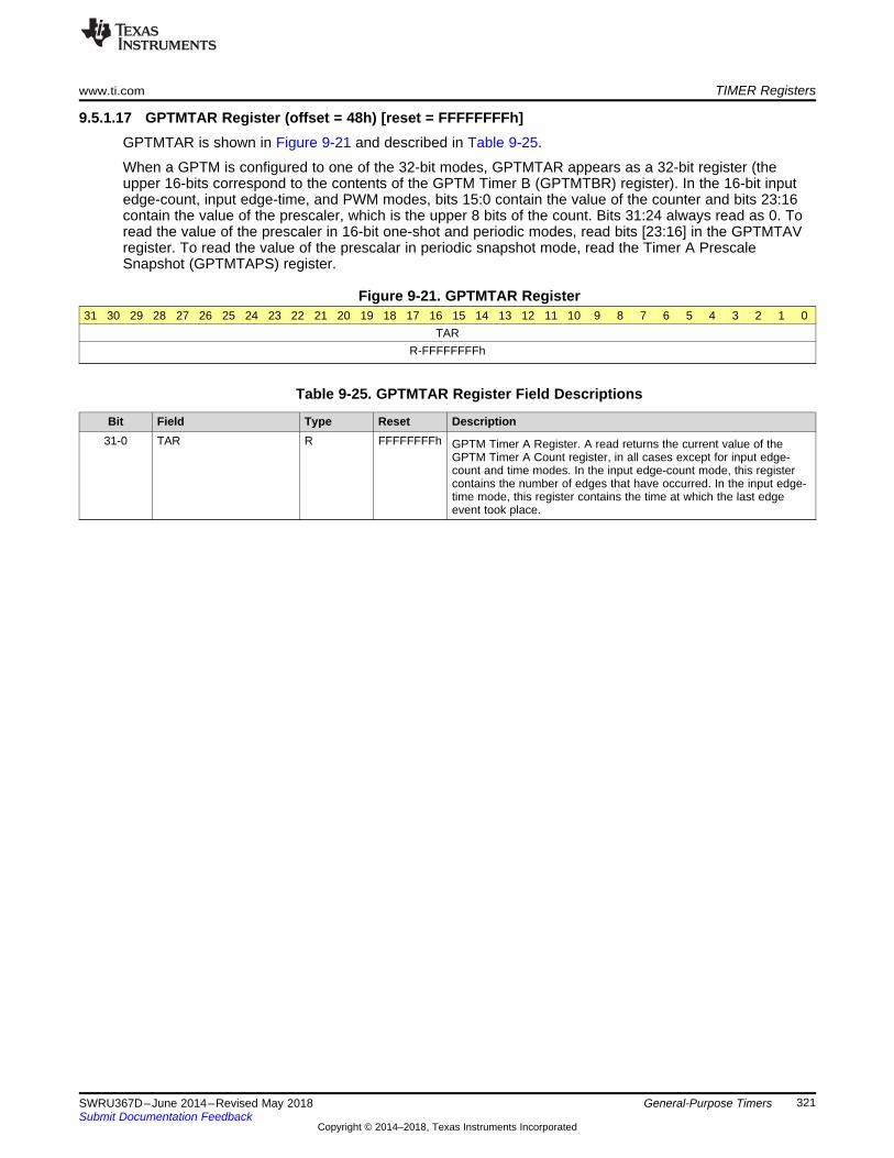
www.ti.com TIMER Registers
321SWRU367D–June 2014–Revised May 2018Submit Documentation Feedback
Copyright © 2014–2018, Texas Instruments Incorporated
General-Purpose Timers
9.5.1.17 GPTMTAR Register (offset = 48h) [reset = FFFFFFFFh]GPTMTAR is shown in Figure 9-21 and described in Table 9-25.
When a GPTM is configured to one of the 32-bit modes, GPTMTAR appears as a 32-bit register (theupper 16-bits correspond to the contents of the GPTM Timer B (GPTMTBR) register). In the 16-bit inputedge-count, input edge-time, and PWM modes, bits 15:0 contain the value of the counter and bits 23:16contain the value of the prescaler, which is the upper 8 bits of the count. Bits 31:24 always read as 0. Toread the value of the prescaler in 16-bit one-shot and periodic modes, read bits [23:16] in the GPTMTAVregister. To read the value of the prescalar in periodic snapshot mode, read the Timer A PrescaleSnapshot (GPTMTAPS) register.
Figure 9-21. GPTMTAR Register31 30 29 28 27 26 25 24 23 22 21 20 19 18 17 16 15 14 13 12 11 10 9 8 7 6 5 4 3 2 1 0
TARR-FFFFFFFFh
Table 9-25. GPTMTAR Register Field Descriptions
Bit Field Type Reset Description31-0 TAR R FFFFFFFFh GPTM Timer A Register. A read returns the current value of the
GPTM Timer A Count register, in all cases except for input edge-count and time modes. In the input edge-count mode, this registercontains the number of edges that have occurred. In the input edge-time mode, this register contains the time at which the last edgeevent took place.
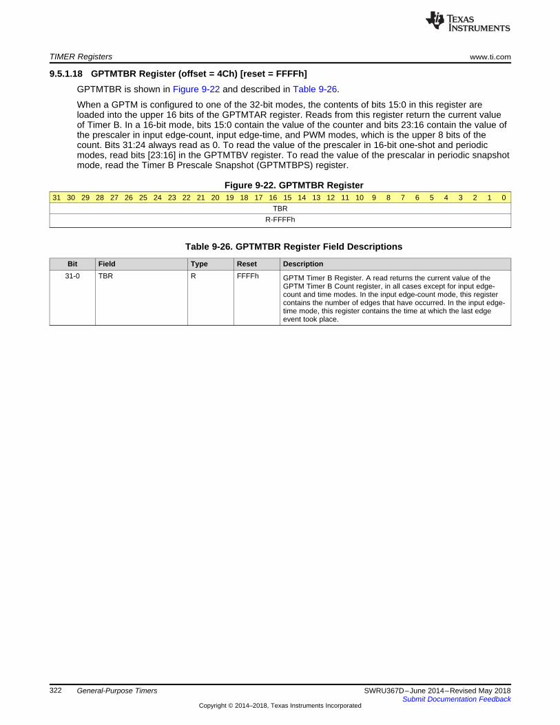
TIMER Registers www.ti.com
322 SWRU367D–June 2014–Revised May 2018Submit Documentation Feedback
Copyright © 2014–2018, Texas Instruments Incorporated
General-Purpose Timers
9.5.1.18 GPTMTBR Register (offset = 4Ch) [reset = FFFFh]GPTMTBR is shown in Figure 9-22 and described in Table 9-26.
When a GPTM is configured to one of the 32-bit modes, the contents of bits 15:0 in this register areloaded into the upper 16 bits of the GPTMTAR register. Reads from this register return the current valueof Timer B. In a 16-bit mode, bits 15:0 contain the value of the counter and bits 23:16 contain the value ofthe prescaler in input edge-count, input edge-time, and PWM modes, which is the upper 8 bits of thecount. Bits 31:24 always read as 0. To read the value of the prescaler in 16-bit one-shot and periodicmodes, read bits [23:16] in the GPTMTBV register. To read the value of the prescalar in periodic snapshotmode, read the Timer B Prescale Snapshot (GPTMTBPS) register.
Figure 9-22. GPTMTBR Register31 30 29 28 27 26 25 24 23 22 21 20 19 18 17 16 15 14 13 12 11 10 9 8 7 6 5 4 3 2 1 0
TBRR-FFFFh
Table 9-26. GPTMTBR Register Field Descriptions
Bit Field Type Reset Description31-0 TBR R FFFFh GPTM Timer B Register. A read returns the current value of the
GPTM Timer B Count register, in all cases except for input edge-count and time modes. In the input edge-count mode, this registercontains the number of edges that have occurred. In the input edge-time mode, this register contains the time at which the last edgeevent took place.

www.ti.com TIMER Registers
323SWRU367D–June 2014–Revised May 2018Submit Documentation Feedback
Copyright © 2014–2018, Texas Instruments Incorporated
General-Purpose Timers
9.5.1.19 GPTMTAV Register (offset = 50h) [reset = FFFFFFFFh]GPTMTAV is shown in Figure 9-23 and described in Table 9-27.
When a 16/32-bit GPTM is configured to one of the 32-bit modes, GPTMTAV appears as a 32-bit register(the upper 16-bits correspond to the contents of the GPTM Timer B Value (GPTMTBV) register). In a 16-bit mode, bits 15:0 contain the value of the counter and bits 23:16 contain the current, free-running valueof the prescaler, which is the upper 8 bits of the count in input edge-count, input edge-time, PWM, andone-shot or periodic up count modes. In one-shot or periodic down count modes, the prescaler stored in23:16 is a true prescaler, meaning bits 23:16 count down before decrementing the value in bits 15:0. Theprescaler in bits 31:24 always reads as 0.
Figure 9-23. GPTMTAV Register31 30 29 28 27 26 25 24 23 22 21 20 19 18 17 16 15 14 13 12 11 10 9 8 7 6 5 4 3 2 1 0
TAVR/W-FFFFFFFFh
Table 9-27. GPTMTAV Register Field Descriptions
Bit Field Type Reset Description31-0 TAV R/W FFFFFFFFh GPTM Timer A Value. A read returns the current, free-running value
of Timer A in all modes. When written, the value written into thisregister is loaded into the GPTMTAR register on the next clockcycle. Note: In 16-bit mode, only the lower 16-bits of the GPTMTAVregister can be written with a new value. Writes to the prescaler bitshave no effect.
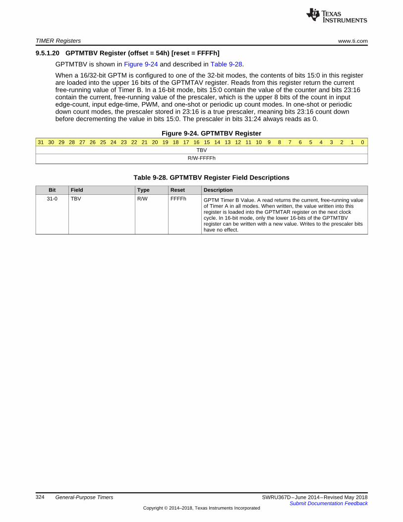
TIMER Registers www.ti.com
324 SWRU367D–June 2014–Revised May 2018Submit Documentation Feedback
Copyright © 2014–2018, Texas Instruments Incorporated
General-Purpose Timers
9.5.1.20 GPTMTBV Register (offset = 54h) [reset = FFFFh]GPTMTBV is shown in Figure 9-24 and described in Table 9-28.
When a 16/32-bit GPTM is configured to one of the 32-bit modes, the contents of bits 15:0 in this registerare loaded into the upper 16 bits of the GPTMTAV register. Reads from this register return the currentfree-running value of Timer B. In a 16-bit mode, bits 15:0 contain the value of the counter and bits 23:16contain the current, free-running value of the prescaler, which is the upper 8 bits of the count in inputedge-count, input edge-time, PWM, and one-shot or periodic up count modes. In one-shot or periodicdown count modes, the prescaler stored in 23:16 is a true prescaler, meaning bits 23:16 count downbefore decrementing the value in bits 15:0. The prescaler in bits 31:24 always reads as 0.
Figure 9-24. GPTMTBV Register31 30 29 28 27 26 25 24 23 22 21 20 19 18 17 16 15 14 13 12 11 10 9 8 7 6 5 4 3 2 1 0
TBVR/W-FFFFh
Table 9-28. GPTMTBV Register Field Descriptions
Bit Field Type Reset Description31-0 TBV R/W FFFFh GPTM Timer B Value. A read returns the current, free-running value
of Timer A in all modes. When written, the value written into thisregister is loaded into the GPTMTAR register on the next clockcycle. In 16-bit mode, only the lower 16-bits of the GPTMTBVregister can be written with a new value. Writes to the prescaler bitshave no effect.
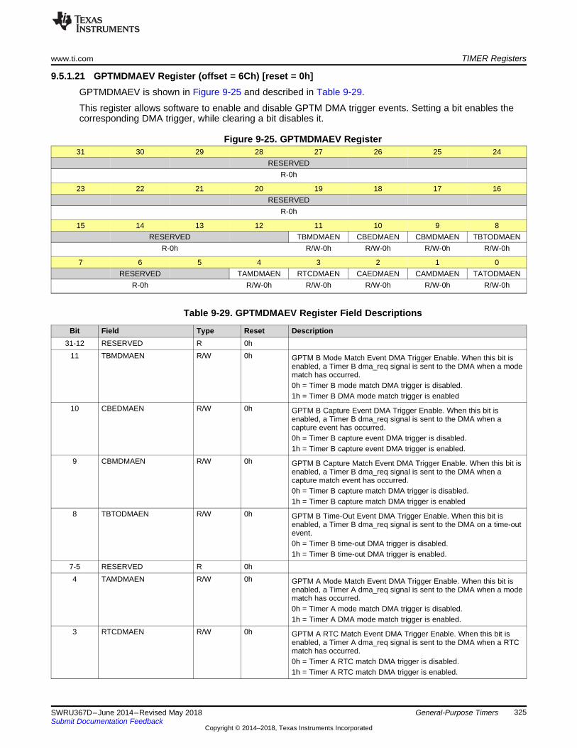
www.ti.com TIMER Registers
325SWRU367D–June 2014–Revised May 2018Submit Documentation Feedback
Copyright © 2014–2018, Texas Instruments Incorporated
General-Purpose Timers
9.5.1.21 GPTMDMAEV Register (offset = 6Ch) [reset = 0h]GPTMDMAEV is shown in Figure 9-25 and described in Table 9-29.
This register allows software to enable and disable GPTM DMA trigger events. Setting a bit enables thecorresponding DMA trigger, while clearing a bit disables it.
Figure 9-25. GPTMDMAEV Register31 30 29 28 27 26 25 24
RESERVEDR-0h
23 22 21 20 19 18 17 16RESERVED
R-0h
15 14 13 12 11 10 9 8RESERVED TBMDMAEN CBEDMAEN CBMDMAEN TBTODMAEN
R-0h R/W-0h R/W-0h R/W-0h R/W-0h
7 6 5 4 3 2 1 0RESERVED TAMDMAEN RTCDMAEN CAEDMAEN CAMDMAEN TATODMAEN
R-0h R/W-0h R/W-0h R/W-0h R/W-0h R/W-0h
Table 9-29. GPTMDMAEV Register Field Descriptions
Bit Field Type Reset Description31-12 RESERVED R 0h
11 TBMDMAEN R/W 0h GPTM B Mode Match Event DMA Trigger Enable. When this bit isenabled, a Timer B dma_req signal is sent to the DMA when a modematch has occurred.0h = Timer B mode match DMA trigger is disabled.1h = Timer B DMA mode match trigger is enabled
10 CBEDMAEN R/W 0h GPTM B Capture Event DMA Trigger Enable. When this bit isenabled, a Timer B dma_req signal is sent to the DMA when acapture event has occurred.0h = Timer B capture event DMA trigger is disabled.1h = Timer B capture event DMA trigger is enabled.
9 CBMDMAEN R/W 0h GPTM B Capture Match Event DMA Trigger Enable. When this bit isenabled, a Timer B dma_req signal is sent to the DMA when acapture match event has occurred.0h = Timer B capture match DMA trigger is disabled.1h = Timer B capture match DMA trigger is enabled
8 TBTODMAEN R/W 0h GPTM B Time-Out Event DMA Trigger Enable. When this bit isenabled, a Timer B dma_req signal is sent to the DMA on a time-outevent.0h = Timer B time-out DMA trigger is disabled.1h = Timer B time-out DMA trigger is enabled.
7-5 RESERVED R 0h4 TAMDMAEN R/W 0h GPTM A Mode Match Event DMA Trigger Enable. When this bit is
enabled, a Timer A dma_req signal is sent to the DMA when a modematch has occurred.0h = Timer A mode match DMA trigger is disabled.1h = Timer A DMA mode match trigger is enabled.
3 RTCDMAEN R/W 0h GPTM A RTC Match Event DMA Trigger Enable. When this bit isenabled, a Timer A dma_req signal is sent to the DMA when a RTCmatch has occurred.0h = Timer A RTC match DMA trigger is disabled.1h = Timer A RTC match DMA trigger is enabled.
TIMER Registers www.ti.com
326 SWRU367D–June 2014–Revised May 2018Submit Documentation Feedback
Copyright © 2014–2018, Texas Instruments Incorporated
General-Purpose Timers
Table 9-29. GPTMDMAEV Register Field Descriptions (continued)Bit Field Type Reset Description2 CAEDMAEN R/W 0h GPTM A Capture Event DMA Trigger Enable. When this bit is
enabled, a Timer A dma_req signal is sent to the DMA when acapture event has occurred.0h = Timer A capture event DMA trigger is disabled.1h = Timer A capture event DMA trigger is enabled.
1 CAMDMAEN R/W 0h GPTM A Capture Match Event DMA Trigger Enable. When this bit isenabled, a Timer A dma_req signal is sent to the DMA when acapture match event has occurred.0h = Timer A capture match DMA trigger is disabled.1h = Timer A capture match DMA trigger is enabled.
0 TATODMAEN R/W 0h GPTM A Time-Out Event DMA Trigger Enable. When this bit isenabled, a Timer A dma_req signal is sent to the DMA on a time-outevent.0h = Timer A time-out DMA trigger is disabled.1h = Timer A time-out DMA trigger is enabled.
327SWRU367D–June 2014–Revised May 2018Submit Documentation Feedback
Copyright © 2014–2018, Texas Instruments Incorporated
Watchdog Timer
Chapter 10SWRU367D–June 2014–Revised May 2018
Watchdog Timer
Topic ........................................................................................................................... Page
10.1 Overview ......................................................................................................... 32810.2 Functional Description ...................................................................................... 32910.3 Register Map.................................................................................................... 32910.4 MCU Watch Dog Controller Usage Caveats.......................................................... 338
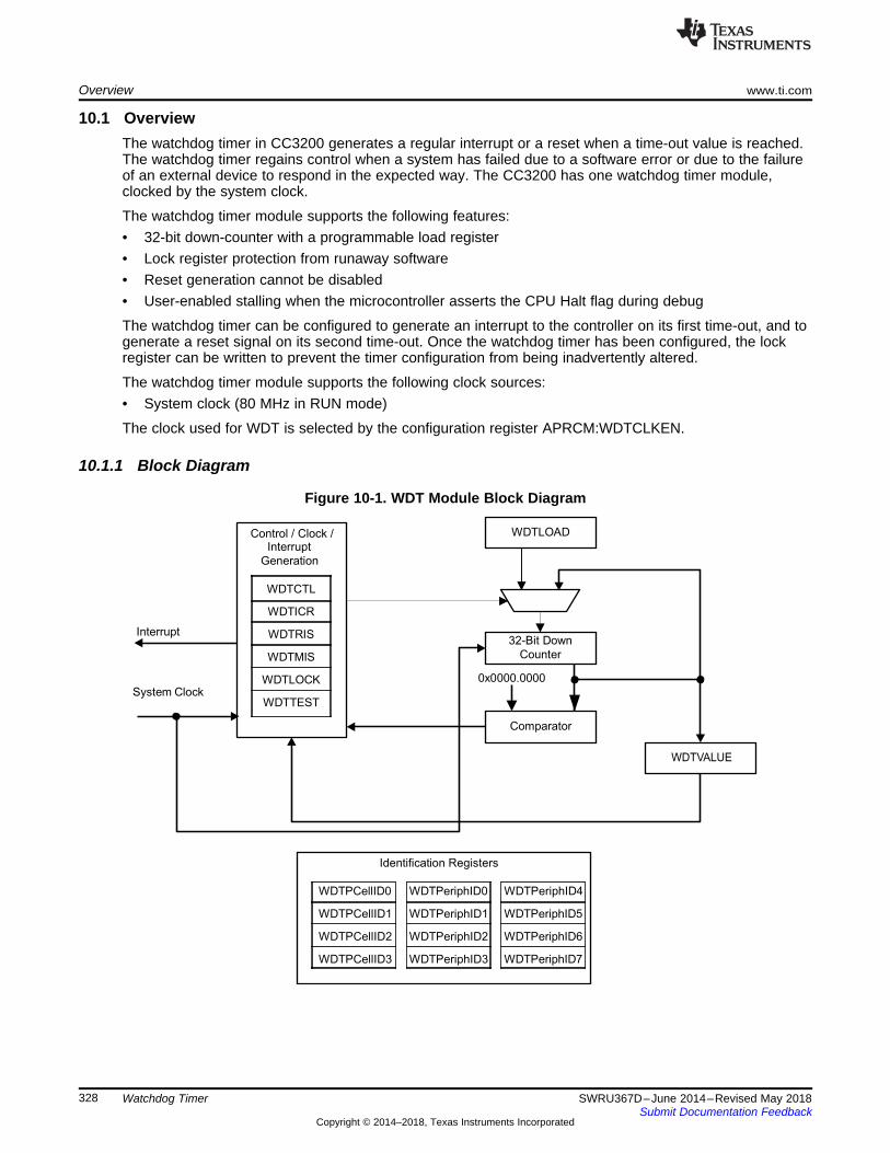
WDTCTL
WDTICR
WDTRIS
WDTMIS
WDTLOCK
WDTTEST
WDTPeriphID0
WDTPeriphID1
WDTPeriphID2
WDTPeriphID3
WDTPeriphID4
WDTPeriphID5
WDTPeriphID6
WDTPeriphID7
Control / Clock /Interrupt
Generation
WDTLOAD
Interrupt
System Clock
32-Bit Down
Counter
0x0000.0000
Comparator
WDTVALUE
Identification Registers
WDTPCellID0
WDTPCellID1
WDTPCellID2
WDTPCellID3
Overview www.ti.com
328 SWRU367D–June 2014–Revised May 2018Submit Documentation Feedback
Copyright © 2014–2018, Texas Instruments Incorporated
Watchdog Timer
10.1 OverviewThe watchdog timer in CC3200 generates a regular interrupt or a reset when a time-out value is reached.The watchdog timer regains control when a system has failed due to a software error or due to the failureof an external device to respond in the expected way. The CC3200 has one watchdog timer module,clocked by the system clock.
The watchdog timer module supports the following features:• 32-bit down-counter with a programmable load register• Lock register protection from runaway software• Reset generation cannot be disabled• User-enabled stalling when the microcontroller asserts the CPU Halt flag during debug
The watchdog timer can be configured to generate an interrupt to the controller on its first time-out, and togenerate a reset signal on its second time-out. Once the watchdog timer has been configured, the lockregister can be written to prevent the timer configuration from being inadvertently altered.
The watchdog timer module supports the following clock sources:• System clock (80 MHz in RUN mode)
The clock used for WDT is selected by the configuration register APRCM:WDTCLKEN.
10.1.1 Block Diagram
Figure 10-1. WDT Module Block Diagram
www.ti.com Functional Description
329SWRU367D–June 2014–Revised May 2018Submit Documentation Feedback
Copyright © 2014–2018, Texas Instruments Incorporated
Watchdog Timer
10.2 Functional DescriptionThe watchdog timer module generates the first time-out signal (interrupt) when the 32-bit counter reachesthe zero state after being enabled; enabling the counter also enables the watchdog timer interrupt. TheWDT can be configured to reset on the second overflow. The WDT interrupt is maskable.
After the first time-out event, the 32-bit counter is re-loaded with the value of the Watchdog Timer Load(WDTLOAD) register, and the timer resumes counting down from that value. Once the watchdog timer hasbeen configured, the Watchdog Timer Lock (WDTLOCK) register is written, which prevents the timerconfiguration from being inadvertently altered by software.
If the timer counts down to its zero state again before the first time-out interrupt is cleared, the watchdogtimer asserts its reset signal to the system. If the interrupt is cleared before the 32-bit counter reaches itssecond time-out, the 32-bit counter is loaded with the value in the WDTLOAD register, and countingresumes from that value.
If WDTLOAD is written with a new value while the watchdog timer counter is counting, then the counter isloaded with the new value, and continues counting.
Writing to WDTLOAD does not clear an active interrupt. An interrupt must be specifically cleared by writingto the Watchdog Interrupt Clear (WDTICR) register.
The watchdog timer is disabled by default out of reset. To achieve maximum watchdog protection of thedevice, the watchdog timer can be enabled at the start of the reset vector.
NOTE: In the CC3200 R1 device, TI recommends that the application software, when rebooting aftera WDT reset, requests the PRCM for hibernation (see Section 15.4.10) for 10 ms, andresumes its full functionality only after returning from this hibernation. This is effective for fullrecovery from any complex stuck-at scenario that involves the Wi-Fi subsystem.
The application can determine if the reset cause is WDT by reading theGPRCM:APPS_RESET_CAUSE[7:0] register (physical address 0×4402 D00C). On wakeup following aWDT reset, this would read the value 0101.
Refer to for more details.
10.2.1 Initialization and Configuration
The watchdog timer is configured using the following sequence:1. Enable the peripheral clock by setting the RUNCLKEN bit in Watchdog Timer Clock Enable
(WDTCLKEN) register.2. Reset the watchdog module using the Watch Dog Timer Software Reset (WDTSWRST) register.3. Load the WDTLOAD register with the desired timer load value.4. Set the INTEN bit in the WDTCTL register to enable the watchdog, enable interrupts, and lock the
control register.
If the software requires that all of the watchdog registers are locked, the watchdog timer module can befully locked by writing any value to the WDTLOCK register. To unlock the watchdog timer, write a value of0x1ACC.E551.
To service the watchdog, periodically reload the count value into the WDTLOAD register to restart thecount. The interrupt can be enabled using the INTEN bit in the WDTCTL register to allow the processor toattempt corrective action if the watchdog is not serviced often enough. The RESEN bit in WDTCTL can beset so that the system resets if the failure is not recoverable using the ISR.
10.3 Register MapTable 10-1 lists the watchdog registers. The offset listed is a hexadecimal increment to the registeraddress, relative to the watchdog timer base address: 0x4000.0000.
Note that the watchdog timer module clock must be enabled before the registers can be programmed.
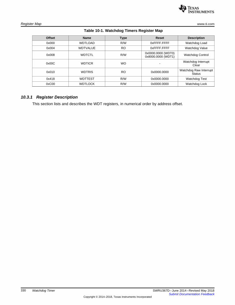
Register Map www.ti.com
330 SWRU367D–June 2014–Revised May 2018Submit Documentation Feedback
Copyright © 2014–2018, Texas Instruments Incorporated
Watchdog Timer
Table 10-1. Watchdog Timers Register Map
Offset Name Type Reset Description0x000 WDTLOAD R/W 0xFFFF.FFFF Watchdog Load0x004 WDTVALUE RO 0xFFFF.FFFF Watchdog Value
0x008 WDTCTL R/W 0x0000.0000 (WDT0)0x8000.0000 (WDT1) Watchdog Control
0x00C WDTICR WO - Watchdog InterruptClear
0x010 WDTRIS RO 0x0000.0000 Watchdog Raw InterruptStatus
0x418 WDTTEST R/W 0x0000.0000 Watchdog Test0xC00 WDTLOCK R/W 0x0000.0000 Watchdog Lock
10.3.1 Register DescriptionThis section lists and describes the WDT registers, in numerical order by address offset.
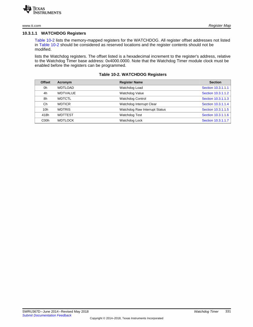
www.ti.com Register Map
331SWRU367D–June 2014–Revised May 2018Submit Documentation Feedback
Copyright © 2014–2018, Texas Instruments Incorporated
Watchdog Timer
10.3.1.1 WATCHDOG RegistersTable 10-2 lists the memory-mapped registers for the WATCHDOG. All register offset addresses not listedin Table 10-2 should be considered as reserved locations and the register contents should not bemodified.
lists the Watchdog registers. The offset listed is a hexadecimal increment to the register's address, relativeto the Watchdog Timer base address: 0x4000.0000. Note that the Watchdog Timer module clock must beenabled before the registers can be programmed.
Table 10-2. WATCHDOG Registers
Offset Acronym Register Name Section0h WDTLOAD Watchdog Load Section 10.3.1.1.14h WDTVALUE Watchdog Value Section 10.3.1.1.28h WDTCTL Watchdog Control Section 10.3.1.1.3Ch WDTICR Watchdog Interrupt Clear Section 10.3.1.1.410h WDTRIS Watchdog Raw Interrupt Status Section 10.3.1.1.5418h WDTTEST Watchdog Test Section 10.3.1.1.6C00h WDTLOCK Watchdog Lock Section 10.3.1.1.7
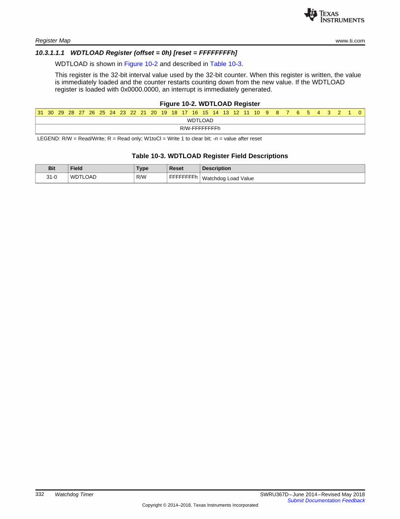
Register Map www.ti.com
332 SWRU367D–June 2014–Revised May 2018Submit Documentation Feedback
Copyright © 2014–2018, Texas Instruments Incorporated
Watchdog Timer
10.3.1.1.1 WDTLOAD Register (offset = 0h) [reset = FFFFFFFFh]WDTLOAD is shown in Figure 10-2 and described in Table 10-3.
This register is the 32-bit interval value used by the 32-bit counter. When this register is written, the valueis immediately loaded and the counter restarts counting down from the new value. If the WDTLOADregister is loaded with 0x0000.0000, an interrupt is immediately generated.
Figure 10-2. WDTLOAD Register31 30 29 28 27 26 25 24 23 22 21 20 19 18 17 16 15 14 13 12 11 10 9 8 7 6 5 4 3 2 1 0
WDTLOADR/W-FFFFFFFFh
LEGEND: R/W = Read/Write; R = Read only; W1toCl = Write 1 to clear bit; -n = value after reset
Table 10-3. WDTLOAD Register Field Descriptions
Bit Field Type Reset Description31-0 WDTLOAD R/W FFFFFFFFh Watchdog Load Value
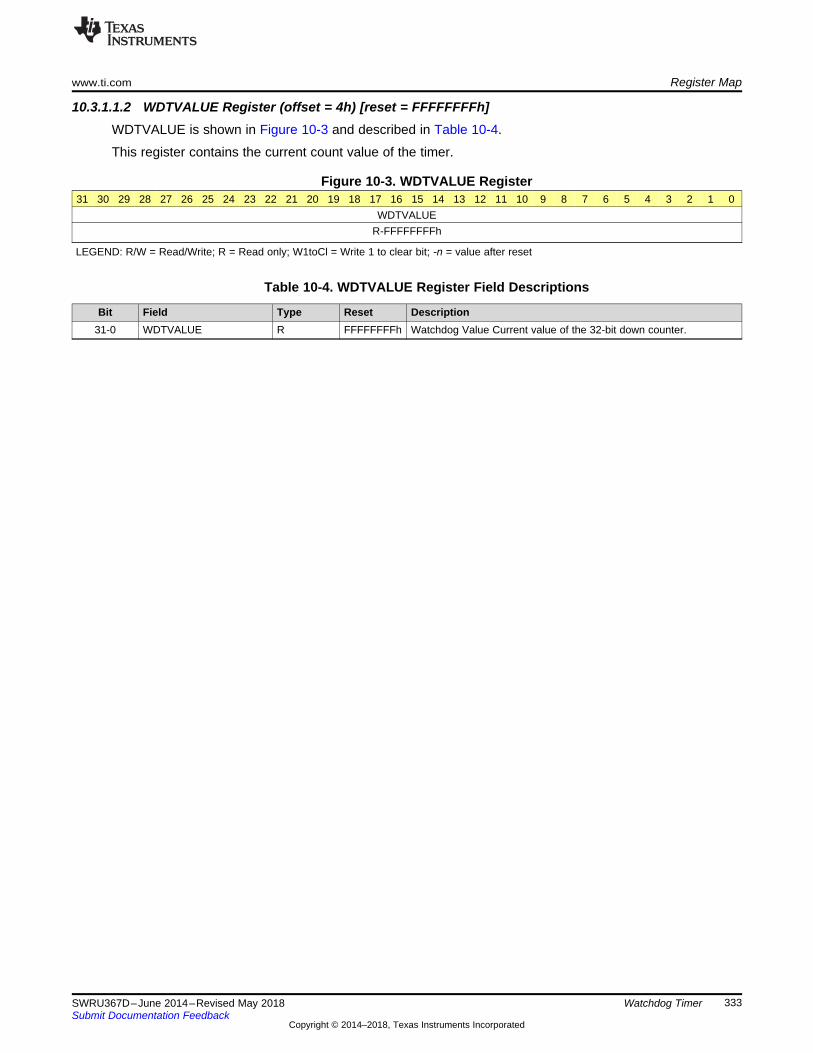
www.ti.com Register Map
333SWRU367D–June 2014–Revised May 2018Submit Documentation Feedback
Copyright © 2014–2018, Texas Instruments Incorporated
Watchdog Timer
10.3.1.1.2 WDTVALUE Register (offset = 4h) [reset = FFFFFFFFh]WDTVALUE is shown in Figure 10-3 and described in Table 10-4.
This register contains the current count value of the timer.
Figure 10-3. WDTVALUE Register31 30 29 28 27 26 25 24 23 22 21 20 19 18 17 16 15 14 13 12 11 10 9 8 7 6 5 4 3 2 1 0
WDTVALUER-FFFFFFFFh
LEGEND: R/W = Read/Write; R = Read only; W1toCl = Write 1 to clear bit; -n = value after reset
Table 10-4. WDTVALUE Register Field Descriptions
Bit Field Type Reset Description31-0 WDTVALUE R FFFFFFFFh Watchdog Value Current value of the 32-bit down counter.
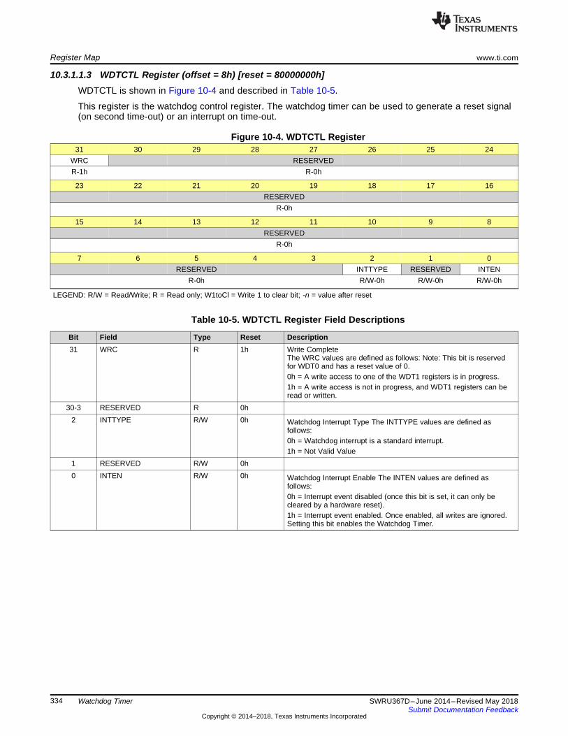
Register Map www.ti.com
334 SWRU367D–June 2014–Revised May 2018Submit Documentation Feedback
Copyright © 2014–2018, Texas Instruments Incorporated
Watchdog Timer
10.3.1.1.3 WDTCTL Register (offset = 8h) [reset = 80000000h]WDTCTL is shown in Figure 10-4 and described in Table 10-5.
This register is the watchdog control register. The watchdog timer can be used to generate a reset signal(on second time-out) or an interrupt on time-out.
Figure 10-4. WDTCTL Register31 30 29 28 27 26 25 24
WRC RESERVEDR-1h R-0h
23 22 21 20 19 18 17 16RESERVED
R-0h
15 14 13 12 11 10 9 8RESERVED
R-0h
7 6 5 4 3 2 1 0RESERVED INTTYPE RESERVED INTEN
R-0h R/W-0h R/W-0h R/W-0h
LEGEND: R/W = Read/Write; R = Read only; W1toCl = Write 1 to clear bit; -n = value after reset
Table 10-5. WDTCTL Register Field Descriptions
Bit Field Type Reset Description31 WRC R 1h Write Complete
The WRC values are defined as follows: Note: This bit is reservedfor WDT0 and has a reset value of 0.0h = A write access to one of the WDT1 registers is in progress.1h = A write access is not in progress, and WDT1 registers can beread or written.
30-3 RESERVED R 0h2 INTTYPE R/W 0h Watchdog Interrupt Type The INTTYPE values are defined as
follows:0h = Watchdog interrupt is a standard interrupt.1h = Not Valid Value
1 RESERVED R/W 0h0 INTEN R/W 0h Watchdog Interrupt Enable The INTEN values are defined as
follows:0h = Interrupt event disabled (once this bit is set, it can only becleared by a hardware reset).1h = Interrupt event enabled. Once enabled, all writes are ignored.Setting this bit enables the Watchdog Timer.
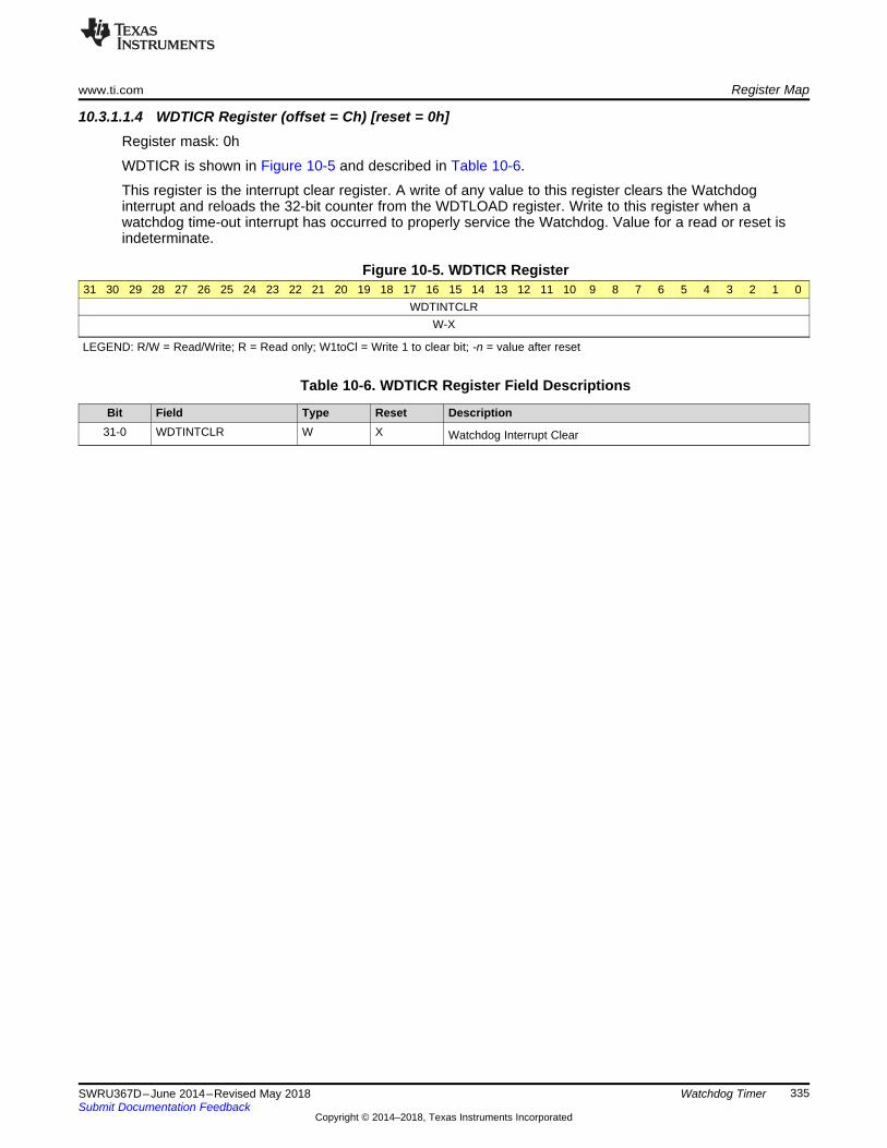
www.ti.com Register Map
335SWRU367D–June 2014–Revised May 2018Submit Documentation Feedback
Copyright © 2014–2018, Texas Instruments Incorporated
Watchdog Timer
10.3.1.1.4 WDTICR Register (offset = Ch) [reset = 0h]Register mask: 0h
WDTICR is shown in Figure 10-5 and described in Table 10-6.
This register is the interrupt clear register. A write of any value to this register clears the Watchdoginterrupt and reloads the 32-bit counter from the WDTLOAD register. Write to this register when awatchdog time-out interrupt has occurred to properly service the Watchdog. Value for a read or reset isindeterminate.
Figure 10-5. WDTICR Register31 30 29 28 27 26 25 24 23 22 21 20 19 18 17 16 15 14 13 12 11 10 9 8 7 6 5 4 3 2 1 0
WDTINTCLRW-X
LEGEND: R/W = Read/Write; R = Read only; W1toCl = Write 1 to clear bit; -n = value after reset
Table 10-6. WDTICR Register Field Descriptions
Bit Field Type Reset Description31-0 WDTINTCLR W X Watchdog Interrupt Clear
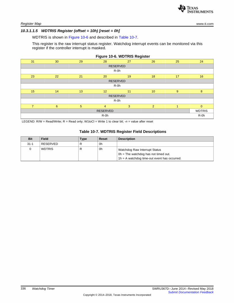
Register Map www.ti.com
336 SWRU367D–June 2014–Revised May 2018Submit Documentation Feedback
Copyright © 2014–2018, Texas Instruments Incorporated
Watchdog Timer
10.3.1.1.5 WDTRIS Register (offset = 10h) [reset = 0h]WDTRIS is shown in Figure 10-6 and described in Table 10-7.
This register is the raw interrupt status register. Watchdog interrupt events can be monitored via thisregister if the controller interrupt is masked.
Figure 10-6. WDTRIS Register31 30 29 28 27 26 25 24
RESERVEDR-0h
23 22 21 20 19 18 17 16RESERVED
R-0h
15 14 13 12 11 10 9 8RESERVED
R-0h
7 6 5 4 3 2 1 0RESERVED WDTRIS
R-0h R-0h
LEGEND: R/W = Read/Write; R = Read only; W1toCl = Write 1 to clear bit; -n = value after reset
Table 10-7. WDTRIS Register Field Descriptions
Bit Field Type Reset Description31-1 RESERVED R 0h
0 WDTRIS R 0h Watchdog Raw Interrupt Status0h = The watchdog has not timed out.1h = A watchdog time-out event has occurred.

www.ti.com Register Map
337SWRU367D–June 2014–Revised May 2018Submit Documentation Feedback
Copyright © 2014–2018, Texas Instruments Incorporated
Watchdog Timer
10.3.1.1.6 WDTTEST Register (offset = 418h) [reset = 0h]WDTTEST is shown in Figure 10-7 and described in Table 10-8.
This register provides user-enabled stalling when the microcontroller asserts the CPU halt flag duringdebug.
Figure 10-7. WDTTEST Register31 30 29 28 27 26 25 24
RESERVEDR-0h
23 22 21 20 19 18 17 16RESERVED
R-0h
15 14 13 12 11 10 9 8RESERVED STALL
R-0h R/W-0h
7 6 5 4 3 2 1 0RESERVED
R-0h
LEGEND: R/W = Read/Write; R = Read only; W1toCl = Write 1 to clear bit; -n = value after reset
Table 10-8. WDTTEST Register Field Descriptions
Bit Field Type Reset Description31-9 RESERVED R 0h
8 STALL R/W 0h Watchdog Stall Enable0h = The watchdog timer continues counting if the microcontroller isstopped with a debugger.1h = If the microcontroller is stopped with a debugger, the watchdogtimer stops counting. Once the microcontroller is restarted, thewatchdog timer resumes counting.
7-0 RESERVED R 0h
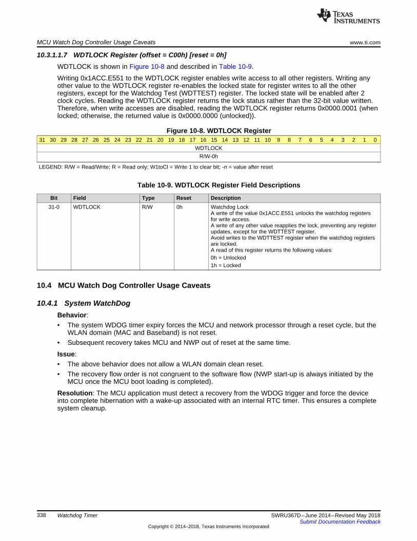
MCU Watch Dog Controller Usage Caveats www.ti.com
338 SWRU367D–June 2014–Revised May 2018Submit Documentation Feedback
Copyright © 2014–2018, Texas Instruments Incorporated
Watchdog Timer
10.3.1.1.7 WDTLOCK Register (offset = C00h) [reset = 0h]WDTLOCK is shown in Figure 10-8 and described in Table 10-9.
Writing 0x1ACC.E551 to the WDTLOCK register enables write access to all other registers. Writing anyother value to the WDTLOCK register re-enables the locked state for register writes to all the otherregisters, except for the Watchdog Test (WDTTEST) register. The locked state will be enabled after 2clock cycles. Reading the WDTLOCK register returns the lock status rather than the 32-bit value written.Therefore, when write accesses are disabled, reading the WDTLOCK register returns 0x0000.0001 (whenlocked; otherwise, the returned value is 0x0000.0000 (unlocked)).
Figure 10-8. WDTLOCK Register31 30 29 28 27 26 25 24 23 22 21 20 19 18 17 16 15 14 13 12 11 10 9 8 7 6 5 4 3 2 1 0
WDTLOCKR/W-0h
LEGEND: R/W = Read/Write; R = Read only; W1toCl = Write 1 to clear bit; -n = value after reset
Table 10-9. WDTLOCK Register Field Descriptions
Bit Field Type Reset Description31-0 WDTLOCK R/W 0h Watchdog Lock
A write of the value 0x1ACC.E551 unlocks the watchdog registersfor write access.A write of any other value reapplies the lock, preventing any registerupdates, except for the WDTTEST register.Avoid writes to the WDTTEST register when the watchdog registersare locked.A read of this register returns the following values:0h = Unlocked1h = Locked
10.4 MCU Watch Dog Controller Usage Caveats
10.4.1 System WatchDogBehavior:• The system WDOG timer expiry forces the MCU and network processor through a reset cycle, but the
WLAN domain (MAC and Baseband) is not reset.• Subsequent recovery takes MCU and NWP out of reset at the same time.
Issue:• The above behavior does not allow a WLAN domain clean reset.• The recovery flow order is not congruent to the software flow (NWP start-up is always initiated by the
MCU once the MCU boot loading is completed).
Resolution: The MCU application must detect a recovery from the WDOG trigger and force the deviceinto complete hibernation with a wake-up associated with an internal RTC timer. This ensures a completesystem cleanup.
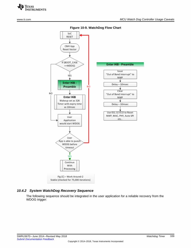
www.ti.com MCU Watch Dog Controller Usage Caveats
339SWRU367D–June 2014–Revised May 2018Submit Documentation Feedback
Copyright © 2014–2018, Texas Instruments Incorporated
Watchdog Timer
Figure 10-9. WatchDog Flow Chart
10.4.2 System WatchDog Recovery SequenceThe following sequence should be integrated in the user application for a reliable recovery from theWDOG trigger:
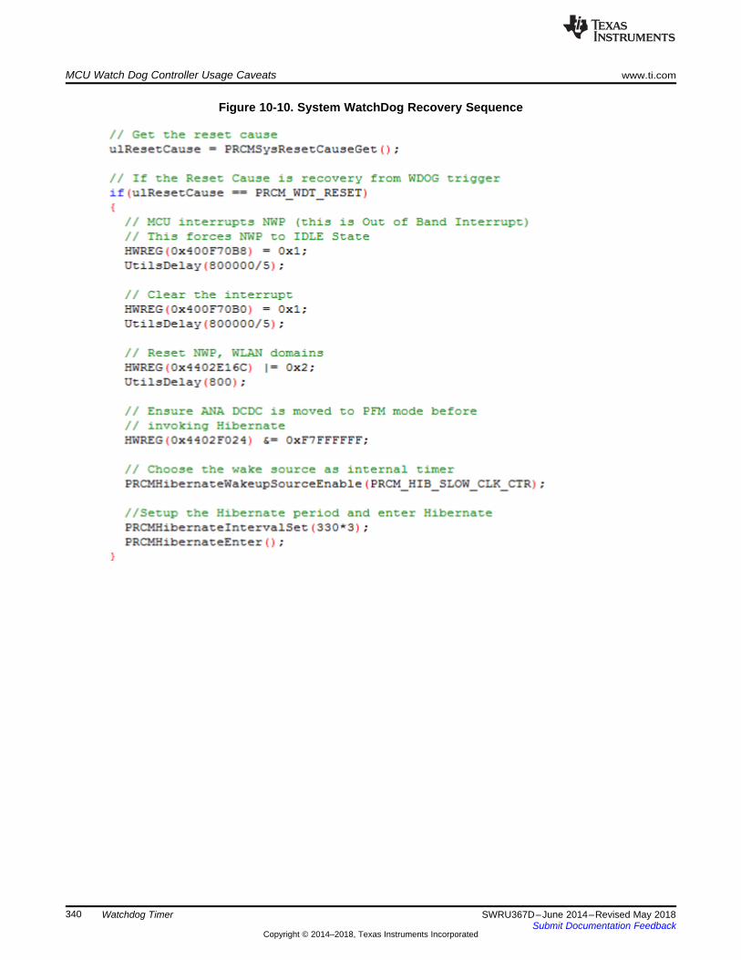
MCU Watch Dog Controller Usage Caveats www.ti.com
340 SWRU367D–June 2014–Revised May 2018Submit Documentation Feedback
Copyright © 2014–2018, Texas Instruments Incorporated
Watchdog Timer
Figure 10-10. System WatchDog Recovery Sequence
341SWRU367D–June 2014–Revised May 2018Submit Documentation Feedback
Copyright © 2014–2018, Texas Instruments Incorporated
SD Host Controller Interface
Chapter 11SWRU367D–June 2014–Revised May 2018
SD Host Controller Interface
Topic ........................................................................................................................... Page
11.1 Overview ......................................................................................................... 34211.2 SD Host Features ............................................................................................. 34211.3 1-Bit SD Interface ............................................................................................. 34311.4 Initialization and Configuration Using Peripheral APIs .......................................... 34311.5 Performance and Testing .................................................................................. 34811.6 Peripheral Library APIs ..................................................................................... 34911.7 Register Description ......................................................................................... 353
Overview www.ti.com
342 SWRU367D–June 2014–Revised May 2018Submit Documentation Feedback
Copyright © 2014–2018, Texas Instruments Incorporated
SD Host Controller Interface
11.1 OverviewThe Secure Digital Host (SD Host) controller on the CC3200 provides an interface between a local host(LH) such as a microprocessor controller (MCU) and an SD memory card, and handles SD transactionswith minimal LH intervention.
The SD host provides SD card access in 1-bit mode, and deals with SD protocol at transmission level,data packing, adding cyclic redundancy checks (CRC), start/end bit, and checking for syntacticalcorrectness. The application interface can send every SD command and either poll for the status of theadapter or wait for an interrupt request, which is sent back in case of exceptions or to warn of end ofoperation. The controller can be configured to generate DMA requests and work with minimum CPUintervention. Given the nature of integration of this peripheral on the CC3200 platform, TI recommendsthat developers use peripheral library APIs to control and operate the block.
This section emphasizes understanding the SD host APIs provided in the CC3200 Software DevelopmentKit [Peripheral Library].
11.2 SD Host Features• Full compliance with SD command and response sets, as defined in the SD memory card.
Specifications, v2.0. Including high-capacity (size >2 GB) cards HC SD.• Flexible architecture, allowing support for new command structure.• 1-bit transfer mode specifications for SD cards• Built-in 1024-byte buffer for read or write
– 512-byte buffer for both transmit and receive– Each buffer is 32-bits wide by 128 words deep
• 32-bit-wide access bus to maximize bus throughput• Single interrupt line for multiple interrupt source events• Two slave DMA channels (1 for TX, 1 for RX)• Programmable clock generation• Integrates an internal transceiver that allows a direct connection to the SD card without external
transceiver.• Supports configurable busy and response timeout.• Support for a wide range of card clock frequency with odd and even clock ratio. Maximum frequency
supported is 24 MHz.
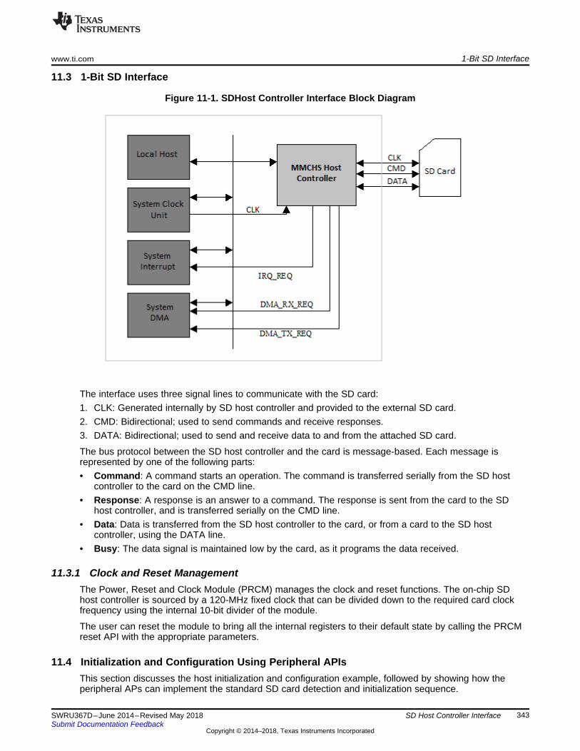
www.ti.com 1-Bit SD Interface
343SWRU367D–June 2014–Revised May 2018Submit Documentation Feedback
Copyright © 2014–2018, Texas Instruments Incorporated
SD Host Controller Interface
11.3 1-Bit SD Interface
Figure 11-1. SDHost Controller Interface Block Diagram
The interface uses three signal lines to communicate with the SD card:1. CLK: Generated internally by SD host controller and provided to the external SD card.2. CMD: Bidirectional; used to send commands and receive responses.3. DATA: Bidirectional; used to send and receive data to and from the attached SD card.
The bus protocol between the SD host controller and the card is message-based. Each message isrepresented by one of the following parts:• Command: A command starts an operation. The command is transferred serially from the SD host
controller to the card on the CMD line.• Response: A response is an answer to a command. The response is sent from the card to the SD
host controller, and is transferred serially on the CMD line.• Data: Data is transferred from the SD host controller to the card, or from a card to the SD host
controller, using the DATA line.• Busy: The data signal is maintained low by the card, as it programs the data received.
11.3.1 Clock and Reset ManagementThe Power, Reset and Clock Module (PRCM) manages the clock and reset functions. The on-chip SDhost controller is sourced by a 120-MHz fixed clock that can be divided down to the required card clockfrequency using the internal 10-bit divider of the module.
The user can reset the module to bring all the internal registers to their default state by calling the PRCMreset API with the appropriate parameters.
11.4 Initialization and Configuration Using Peripheral APIsThis section discusses the host initialization and configuration example, followed by showing how theperipheral APs can implement the standard SD card detection and initialization sequence.
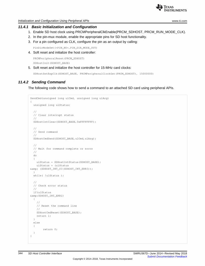
Initialization and Configuration Using Peripheral APIs www.ti.com
344 SWRU367D–June 2014–Revised May 2018Submit Documentation Feedback
Copyright © 2014–2018, Texas Instruments Incorporated
SD Host Controller Interface
11.4.1 Basic Initialization and Configuration1. Enable SD host clock using PRCMPeripheralClkEnable(PRCM_SDHOST, PRCM_RUN_MODE_CLK).2. In the pin-mux module, enable the appropriate pins for SD host functionality.3. For a pin configured as CLK, configure the pin as an output by calling:
PinDirModeSet(<PIN_NO>,PIN_DIR_MODE_OUT)
4. Soft reset and initialize the host controller:
PRCMPeripheralReset(PRCM_SDHOST)
SDHostInit(SDHOST_BASE)
5. Soft reset and initialize the host controller for 15-MHz card clocks:
SDHostSetExpClk(SDHOST_BASE, PRCMPeripheralClockGet(PRCM_SDHOST), 15000000)
11.4.2 Sending CommandThe following code shows how to send a command to an attached SD card using peripheral APIs.
SendCmd(unsigned long ulCmd, unsigned long ulArg)
unsigned long ulStatus;
//// Clear interrupt status//SDHostIntClear(SDHOST_BASE,0xFFFFFFFF);
//// Send command//SDHostCmdSend(SDHOST_BASE,ulCmd,ulArg);
//// Wait for command complete or error//do
ulStatus = SDHostIntStatus(SDHOST_BASE);ulStatus = (ulStatus
& (SDHOST_INT_CC|SDHOST_INT_ERRI));while( !ulStatus );
//// Check error status//if(ulStatus
&SDHOST_INT_ERRI)
//// Reset the command line//SDHostCmdReset(SDHOST_BASE);return 1;
else
return 0;
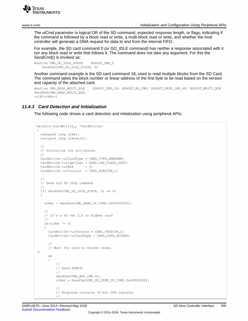
www.ti.com Initialization and Configuration Using Peripheral APIs
345SWRU367D–June 2014–Revised May 2018Submit Documentation Feedback
Copyright © 2014–2018, Texas Instruments Incorporated
SD Host Controller Interface
The ulCmd parameter is logical OR of the SD command, expected response length, or flags, indicating ifthe command is followed by a block read or write, a multi-block read or write, and whether the hostcontroller will generate a DMA request for data to and from the internal FIFO.
For example, the SD card command 0 (or GO_IDLE command) has neither a response associated with itnor any block read or write that follows it. The command does not take any argument. For this theSendCmd() is invoked as:#define CMD_GO_IDLE_STATE SDHOST_CMD_0
SendCmd(CMD_GO_IDLE_STATE, 0)
Another command example is the SD card command 18, used to read multiple blocks from the SD Card.The command takes the block number or linear address of the first byte to be read based on the versionand capacity of the attached card:#define CMD_READ_MULTI_BLK SDHOST_CMD_18| SDHOST_RD_CMD| SDHOST_RESP_LEN_48| SDHOST_MULTI_BLKSendCmd(CMD_READ_MULTI_BLK,<ulBlockNo>)
11.4.3 Card Detection and InitializationThe following code shows a card detection and initialization using peripheral APIs:
CardInit(CardAttrib_t *CardAttrib)
unsigned long ulRet;unsigned long ulResp[4];
//// Initialize the attributes.//CardAttrib->ulCardType = CARD_TYPE_UNKNOWN;CardAttrib->ulCapClass = CARD_CAP_CLASS_SDSC;CardAttrib->ulRCA = 0;CardAttrib->ulVersion = CARD_VERSION_1;
//// Send std GO IDLE command//if( SendCmd(CMD_GO_IDLE_STATE, 0) == 0)
ulRet = SendCmd(CMD_SEND_IF_COND,0x00000100);
//// It's a SD ver 2.0 or higher card//if(ulRet == 0)
CardAttrib->ulVersion = CARD_VERSION_2;CardAttrib->ulCardType = CARD_TYPE_SDCARD;
//// Wait for card to become ready.
//do
//// Send ACMD41//SendCmd(CMD_APP_CMD,0);ulRet = SendCmd(CMD_SD_SEND_OP_COND,0x40E00000);
//// Response contains 32-bit OCR register//
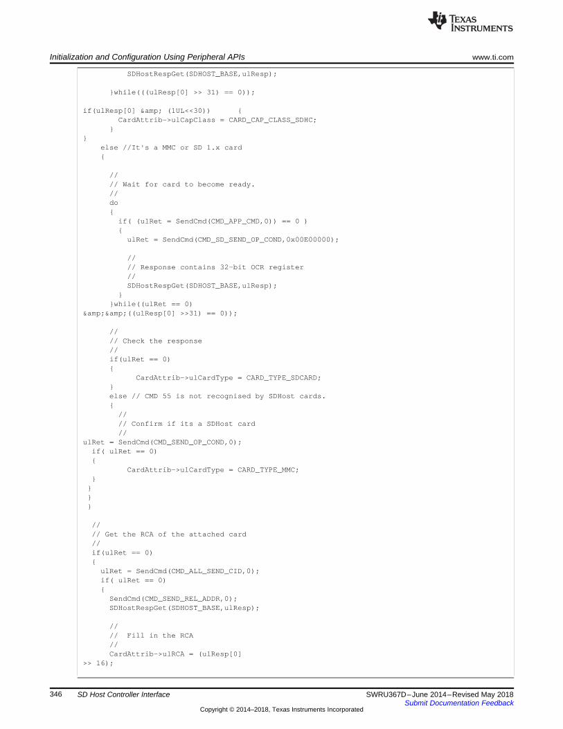
Initialization and Configuration Using Peripheral APIs www.ti.com
346 SWRU367D–June 2014–Revised May 2018Submit Documentation Feedback
Copyright © 2014–2018, Texas Instruments Incorporated
SD Host Controller Interface
SDHostRespGet(SDHOST_BASE,ulResp);
while(((ulResp[0] >> 31) == 0));
if(ulResp[0] & (1UL<<30)) CardAttrib->ulCapClass = CARD_CAP_CLASS_SDHC;
else //It's a MMC or SD 1.x card
//// Wait for card to become ready.//do
if( (ulRet = SendCmd(CMD_APP_CMD,0)) == 0 )
ulRet = SendCmd(CMD_SD_SEND_OP_COND,0x00E00000);
//// Response contains 32-bit OCR register//SDHostRespGet(SDHOST_BASE,ulResp);
while((ulRet == 0)
&&((ulResp[0] >>31) == 0));
//// Check the response//if(ulRet == 0)
CardAttrib->ulCardType = CARD_TYPE_SDCARD;else // CMD 55 is not recognised by SDHost cards.
//// Confirm if its a SDHost card//
ulRet = SendCmd(CMD_SEND_OP_COND,0);if( ulRet == 0)
CardAttrib->ulCardType = CARD_TYPE_MMC;
//// Get the RCA of the attached card//if(ulRet == 0)
ulRet = SendCmd(CMD_ALL_SEND_CID,0);if( ulRet == 0)
SendCmd(CMD_SEND_REL_ADDR,0);SDHostRespGet(SDHOST_BASE,ulResp);
//// Fill in the RCA//CardAttrib->ulRCA = (ulResp[0]
>> 16);
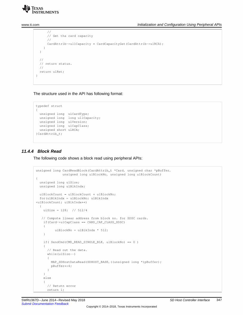
www.ti.com Initialization and Configuration Using Peripheral APIs
347SWRU367D–June 2014–Revised May 2018Submit Documentation Feedback
Copyright © 2014–2018, Texas Instruments Incorporated
SD Host Controller Interface
//// Get tha card capacity//CardAttrib->ullCapacity = CardCapacityGet(CardAttrib->ulRCA);
//// return status.//return ulRet;
The structure used in the API has following format:
typedef struct
unsigned long ulCardType;unsigned long long ullCapacity;unsigned long ulVersion;unsigned long ulCapClass;unsigned short ulRCA;
CardAttrib_t;
11.4.4 Block ReadThe following code shows a block read using peripheral APIs:
unsigned long CardReadBlock(CardAttrib_t *Card, unsigned char *pBuffer,unsigned long ulBlockNo, unsigned long ulBlockCount)
unsigned long ulSize;unsigned long ulBlkIndx;
ulBlockCount = ulBlockCount + ulBlockNo;for(ulBlkIndx = ulBlockNo; ulBlkIndx
<ulBlockCount; ulBlkIndx++)
ulSize = 128; // 512/4
// Compute linear address from block no. for SDSC cards.if(Card->ulCapClass == CARD_CAP_CLASS_SDSC)
ulBlockNo = ulBlkIndx * 512;
if( SendCmd(CMD_READ_SINGLE_BLK, ulBlockNo) == 0 )
// Read out the data.while(ulSize--)
MAP_SDHostDataRead(SDHOST_BASE,((unsigned long *)pBuffer);pBuffer+=4;
else
// Retutn errorreturn 1;
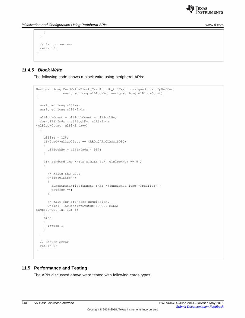
Initialization and Configuration Using Peripheral APIs www.ti.com
348 SWRU367D–June 2014–Revised May 2018Submit Documentation Feedback
Copyright © 2014–2018, Texas Instruments Incorporated
SD Host Controller Interface
// Return successreturn 0;
11.4.5 Block WriteThe following code shows a block write using peripheral APIs:
Unsigned long CardWriteBlock(CardAttrib_t *Card, unsigned char *pBuffer,unsigned long ulBlockNo, unsigned long ulBlockCount)
unsigned long ulSize;unsigned long ulBlkIndx;
ulBlockCount = ulBlockCount + ulBlockNo;for(ulBlkIndx = ulBlockNo; ulBlkIndx
<ulBlockCount; ulBlkIndx++)
ulSize = 128;if(Card->ulCapClass == CARD_CAP_CLASS_SDSC)
ulBlockNo = ulBlkIndx * 512;
if( SendCmd(CMD_WRITE_SINGLE_BLK, ulBlockNo) == 0 )
// Write the datawhile(ulSize--)
SDHostDataWrite(SDHOST_BASE,*((unsigned long *)pBuffer));pBuffer+=4;
// Wait for transfer completion.while( !(SDHostIntStatus(SDHOST_BASE)
&SDHOST_INT_TC) );else
return 1;
// Return errorreturn 0;
11.5 Performance and TestingThe APIs discussed above were tested with following cards types:

www.ti.com Peripheral Library APIs
349SWRU367D–June 2014–Revised May 2018Submit Documentation Feedback
Copyright © 2014–2018, Texas Instruments Incorporated
SD Host Controller Interface
Table 11-1. Card Types
Vendor Size Capacity Class Block Read/Write CommentsTranscend 2 GB SDSC PassedTranscend 16 GB SDHC PassedStrontium 2 GB SDSC Passed
SanDisk 2 GB SDSC Passed
This card requires someadditional delay after thecard select command is
sent to the card, andbefore sending a read orwrite command, or thecommand will never
complete.
SanDisk 64 GB SDXC Passed
This card requires someadditional delay after thecard select command is
sent to the card, andbefore sending a read orwrite command, or thecommand will never
complete.
Kingston 16 GB SDHCFailed. Did not respond
to block read/writecommands
This card requires aspecial SW sequence to
work properly. Theinitialization sequence is
different from othercards.
Table 11-2 shows examples of throughput data using the CPU. These values were measured with 1-MBand 10-MB block read or write on a Class-4 Transcend 16-GB SDHC card:
Table 11-2. Throughput Data
Vendor andType Operation Card Freq 80-MHz Cycles Data (bytes) Baud
(bytes/sec)Throughput
(Mbps)
Class 4Transcend
Read 24 67959516 1048576 1234354 9.4Read 24 680884716 10485760 1232016 9.4Write 12 236784547 1048576 354272 2.70Write 12 2442413554 10485760 343456 2.62Write 24 2151815366 10485760 389839 2.97Write 24 2152352658 10485760 389741 2.97
11.6 Peripheral Library APIsThis section lists the APIs, hosted in the CC3200 SDK (peripheral library) necessary for I2S configuration.
void SDHostInit(unsigned long ulBase)• Description: This function configures the SD host module, enabling internal sub-modules.• Parameters: ulBase – Base address of the SD host module• Return: None
void SDHostCmdReset(unsigned long ulBase)• Description: This function resets the SD host command line.• Parameters: ulBase – Base address of the SD host module• Return: None
long SDHostCmdSend(unsigned long ulBase,unsigned long ulCmd, unsigned ulArg)• Description: This function sends a command to the attached card over the SD host interface.
Peripheral Library APIs www.ti.com
350 SWRU367D–June 2014–Revised May 2018Submit Documentation Feedback
Copyright © 2014–2018, Texas Instruments Incorporated
SD Host Controller Interface
• Parameters:– ulBase – Base address of the SD host module– ulCmd – Command to be send to the card– ulArg – Argument for the commandThe ulCmd parameter can be one of SDHOST_CMD_0 to SDHOST_CMD_63. It can be logicallyORed with one or more of the following:– SDHOST_MULTI_BLK: For multi-block transfer– SDHOST_WR_CMD: If the command is followed by write data– SDHOST_RD_CMD: If the command is followed by read data– SDHOST_DMA_EN: If data transfer must generate a DMA request
• Return: Returns 0 on success, -1 otherwise
void SDHostIntRegister(unsigned long ulBase, void (*pfnHandler)(void))• Description: This function registers the interrupt handler and enables the global interrupt in the
interrupt controller; specific interrupts must be enabled using SDHostIntEnable(). It is the responsibilityof the interrupt handler to clear the interrupt source.
• Parameters:– ulBase – Base address of the SD host module– pfnHandler – Pointer to the SD host interrupt handler function
• Return: None
void SDHostIntUnregister(unsigned long ulBase)• Description: This function unregisters the interrupt handler and clears the handler to be called when a
SD host interrupt occurs. This also masks off the interrupt in the interrupt controller, so that theinterrupt handler is no longer called.
• Parameters: ulBase – Base address of the SD host module• Return: None
void SDHostIntEnable(unsigned long ulBase,unsigned long ulIntFlags)• Description: This function enables the indicated SD host interrupt sources. Only enabled sources can
be reflected to the processor interrupt; disabled sources have no effect on the processor.• Parameters:
– ulBase – Base address of the SD host module– ulIntFlags – Bit mask of the interrupt sources to be enabledThe ulIntFlags parameter is the logical OR of any of the following:– SDHOST_INT_CC: Command Complete interrupt– SDHOST_INT_TC: Transfer Complete interrupt– SDHOST_INT_BWR: Buffer Write Ready interrupt– SDHOST_INT_BWR: Buffer Read Ready interrupt– SDHOST_INT_ERRI: Error interrupt
• Note that SDHOST_INT_ERRI can only be used with SDHostIntStatus(), and is internally logicalOR of all error status bits. Setting this bit alone as ulIntFlags does not generate any interrupt.
– SDHOST_INT_CTO: Command Timeout error interrupt– SDHOST_INT_CEB: Command End Bit error interrupt– SDHOST_INT_DTO: Data Timeout error interrupt– SDHOST_INT_DCRC: Data CRC error interrupt– SDHOST_INT_DEB: Data End Bit error– SDHOST_INT_CERR: Cart Status Error interrupt– SDHOST_INT_BADA: Bad Data error interrupt– SDHOST_INT_DMARD: Read DMA done interrupt
www.ti.com Peripheral Library APIs
351SWRU367D–June 2014–Revised May 2018Submit Documentation Feedback
Copyright © 2014–2018, Texas Instruments Incorporated
SD Host Controller Interface
– SDHOST_INT_DMAWR: Write DMA done interrupt• Return: None
void SDHostIntDisable(unsigned long ulBase,unsigned long ulIntFlags)• Description: This function disables the indicated SD host interrupt sources. Only enabled sources can
be reflected to the processor interrupt.• Parameters:
– ulBase – Base address of the SD host module– ulIntFlags – Bit mask of the interrupt sources to be disabledThe ulIntFlags parameter has the same definition as the ulIntFlags parameter to SDHostIntEnable().
• Return: None
unsigned long SDHostIntStatus(unsigned long ulBase)• Description: This function returns the interrupt status for the specified SD host.• Parameters: ulBase – Base address of the SD host module.• Return: Returns the current interrupt status, enumerated as a bit field of values described in
SDHostIntEnable().
void SDHostIntClear(unsigned long ulBase,unsigned long ulIntFlags)• Description: The specified SD host interrupt sources are cleared, so that they no longer assert. This
function must be called in the interrupt handler to keep the interrupt from being recognized againimmediately upon exit.
• Parameters:– ulBase – Base address of the SD host module– ulIntFlags – Bit mask of the interrupt sources to be clearedThe ulIntFlags parameter has the same definition as the ulIntFlags parameter to SDHostIntEnable().
• Return: None
Void SDHostCardErrorMaskSet(unsigned long ulBase, unsigned long ulErrMask)• Description: This function sets the card status error mask for response type R1, R1b, R5, R5b, and
R6. The parameter ulErrMask is the bit mask of card status errors to be enabled; if the correspondingbits in the card status field of a response are set, then the host controller indicates a card errorinterrupt status. Only bits referenced as type E (error) in the status field in the response can set a cardstatus error.
• Parameters:– ulBase – Base address of the SD host module– ulErrMask – Bit mask of card status errors to be enabled
• Return: None
unsigned long SDHostCardErrorMaskGet(unsigned long ulBase)• Description: This function gets the card status error mask for response type R1, R1b, R5, R5b, and
R6.• Parameters: ulBase – Base address of the SD host module• Return: Returns the current card status error.
void SDHostSetExpClk(unsigned long ulBase, unsigned long ulSDHostClk, unsigned longulCardClk)• Description: This function configures the SD host interface to supply the specified clock to the
connected card.• Parameters:
– ulBase – Base address of the SD host module– ulSDHostClk – The rate of clock supplied to SD host module– ulCardClk – Required SD interface clock
• Return: None
Peripheral Library APIs www.ti.com
352 SWRU367D–June 2014–Revised May 2018Submit Documentation Feedback
Copyright © 2014–2018, Texas Instruments Incorporated
SD Host Controller Interface
void SDHostRespGet(unsigned long ulBase, unsigned long ulRespnse[4])• Description: This function gets the response from the SD card for the last command send.• Parameters:
– ulBase – Base address of the SD host module– ulRespnse – 128-bit response
• Return: None
void SDHostBlockSizeSet(unsigned long ulBase, unsigned short ulBlkSize)• Description: This function sets the block size of the data transfer.• Parameters:
– ulBase – Base address of the SD host module– ulBlkSize – Transfer block size in bytesThe parameter ulBlkSize is size of each data block in bytes. This should be in range 0 -2^10.
• Return: None
void SDHostBlockCountSet(unsigned long ulBase, unsigned short ulBlkCount)• Description: This function sets block count for the data transfer. This must be set for each block
transfer.• Parameters:
– ulBase – Base address of the SD host module– ulBlkCount – Number of blocks
• Return: None
tBoolean SDHostDataNonBlockingWrite(unsigned long ulBase, unsigned long ulData)• Description: This function writes a single data word into the SD host write buffer. The function returns
true if there was a space available in the buffer; else returns false.• Parameters:
– ulBase – Base address of the SD host module– ulData – Data word to be transferred
• Return: Return true on success, false otherwise
tBoolean SDHostDataNonBlockingRead(unsigned long ulBase, unsigned long *pulData)• Description: This function reads a data word from the SD host read buffer. The function returns true if
there was data available in the buffer; else returns false.• Parameters:
– ulBase – Base address of the SD host module– pulData – Pointer to data word to be transferred
• Return: Return true on success, false otherwise
void SDHostDataWrite(unsigned long ulBase, unsigned long ulData)• Description: This function writes \e ulData into the SD host write buffer. If there is no space in the
write buffer, this function waits until there is a space available before returning.• Parameters:
– ulBase – Base address of the SD host module– ulData – Data word to be transferred
• Return: None
void SDHostDataRead(unsigned long ulBase, unsigned long *ulData)• Description: This function reads a single data word from the SD host read buffer. If there is no data
available in the buffer, the function waits until a data word is received before returning.• Parameters:
– ulBase – Base address of the SD host module
www.ti.com Register Description
353SWRU367D–June 2014–Revised May 2018Submit Documentation Feedback
Copyright © 2014–2018, Texas Instruments Incorporated
SD Host Controller Interface
– pulData – Pointer to data word to be transferred• Return: None
11.7 Register Description
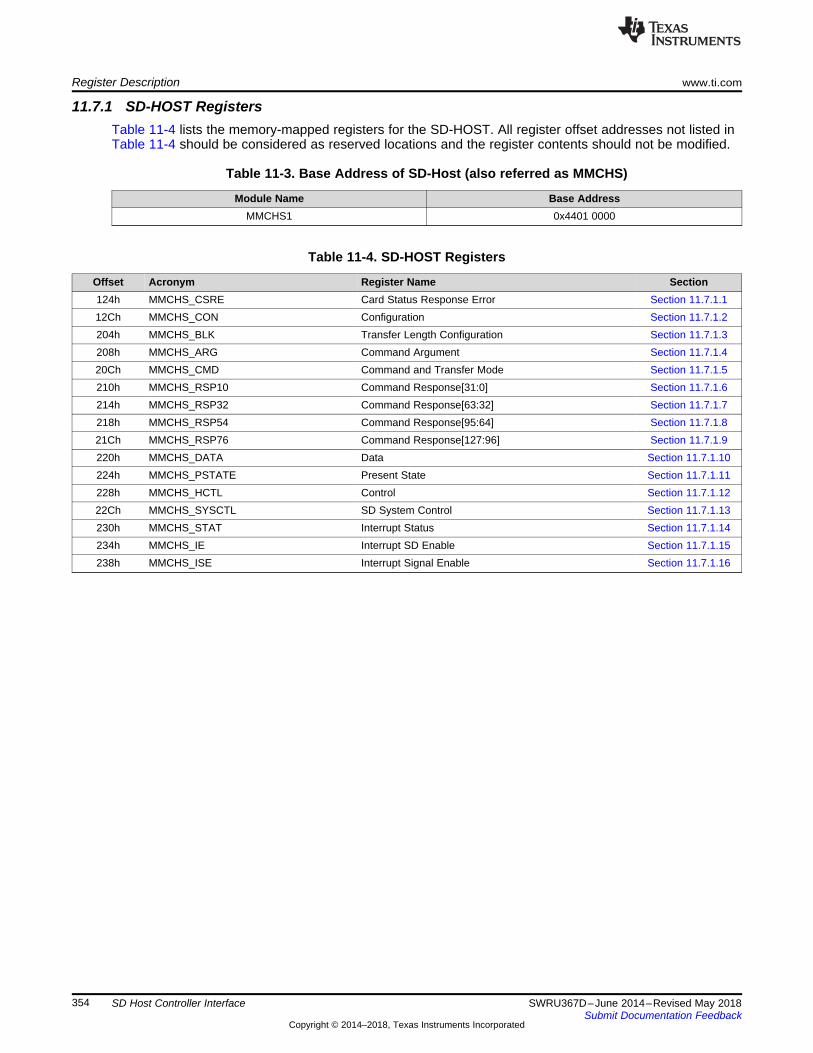
Register Description www.ti.com
354 SWRU367D–June 2014–Revised May 2018Submit Documentation Feedback
Copyright © 2014–2018, Texas Instruments Incorporated
SD Host Controller Interface
11.7.1 SD-HOST RegistersTable 11-4 lists the memory-mapped registers for the SD-HOST. All register offset addresses not listed inTable 11-4 should be considered as reserved locations and the register contents should not be modified.
Table 11-3. Base Address of SD-Host (also referred as MMCHS)
Module Name Base AddressMMCHS1 0x4401 0000
Table 11-4. SD-HOST Registers
Offset Acronym Register Name Section124h MMCHS_CSRE Card Status Response Error Section 11.7.1.112Ch MMCHS_CON Configuration Section 11.7.1.2204h MMCHS_BLK Transfer Length Configuration Section 11.7.1.3208h MMCHS_ARG Command Argument Section 11.7.1.420Ch MMCHS_CMD Command and Transfer Mode Section 11.7.1.5210h MMCHS_RSP10 Command Response[31:0] Section 11.7.1.6214h MMCHS_RSP32 Command Response[63:32] Section 11.7.1.7218h MMCHS_RSP54 Command Response[95:64] Section 11.7.1.821Ch MMCHS_RSP76 Command Response[127:96] Section 11.7.1.9220h MMCHS_DATA Data Section 11.7.1.10224h MMCHS_PSTATE Present State Section 11.7.1.11228h MMCHS_HCTL Control Section 11.7.1.1222Ch MMCHS_SYSCTL SD System Control Section 11.7.1.13230h MMCHS_STAT Interrupt Status Section 11.7.1.14234h MMCHS_IE Interrupt SD Enable Section 11.7.1.15238h MMCHS_ISE Interrupt Signal Enable Section 11.7.1.16
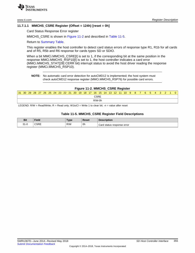
www.ti.com Register Description
355SWRU367D–June 2014–Revised May 2018Submit Documentation Feedback
Copyright © 2014–2018, Texas Instruments Incorporated
SD Host Controller Interface
11.7.1.1 MMCHS_CSRE Register (Offset = 124h) [reset = 0h]Card Status Response Error register
MMCHS_CSRE is shown in Figure 11-2 and described in Table 11-5.
Return to Summary Table.
This register enables the host controller to detect card status errors of response type R1, R1b for all cardsand of R5, R5b and R6 response for cards types SD or SDIO.
When a bit MMCi.MMCHS_CSRE[I] is set to 1, if the corresponding bit at the same position in theresponse MMCi.MMCHS_RSP10[I] is set to 1, the host controller indicates a card error(MMCi.MMCHS_STAT[28] CERR bit) interrupt status to avoid the host driver reading the responseregister (MMCi.MMCHS_RSP10).
NOTE: No automatic card error detection for autoCMD12 is implemented; the host system mustcheck autoCMD12 response register (MMCi.MMCHS_RSP76) for possible card errors.
Figure 11-2. MMCHS_CSRE Register31 30 29 28 27 26 25 24 23 22 21 20 19 18 17 16 15 14 13 12 11 10 9 8 7 6 5 4 3 2 1 0
CSRER/W-0h
LEGEND: R/W = Read/Write; R = Read only; W1toCl = Write 1 to clear bit; -n = value after reset
Table 11-5. MMCHS_CSRE Register Field Descriptions
Bit Field Type Reset Description31-0 CSRE R/W 0h Card status response error
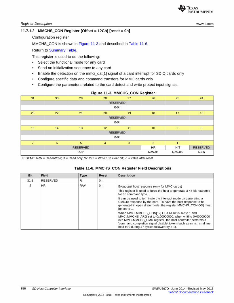
Register Description www.ti.com
356 SWRU367D–June 2014–Revised May 2018Submit Documentation Feedback
Copyright © 2014–2018, Texas Instruments Incorporated
SD Host Controller Interface
11.7.1.2 MMCHS_CON Register (Offset = 12Ch) [reset = 0h]Configuration register
MMCHS_CON is shown in Figure 11-3 and described in Table 11-6.
Return to Summary Table.
This register is used to do the following:• Select the functional mode for any card• Send an initialization sequence to any card• Enable the detection on the mmci_dat[1] signal of a card interrupt for SDIO cards only• Configure specific data and command transfers for MMC cards only• Configure the parameters related to the card detect and write protect input signals.
Figure 11-3. MMCHS_CON Register31 30 29 28 27 26 25 24
RESERVEDR-0h
23 22 21 20 19 18 17 16RESERVED
R-0h
15 14 13 12 11 10 9 8RESERVED
R-0h
7 6 5 4 3 2 1 0RESERVED HR INIT RESERVED
R-0h R/W-0h R/W-0h R-0h
LEGEND: R/W = Read/Write; R = Read only; W1toCl = Write 1 to clear bit; -n = value after reset
Table 11-6. MMCHS_CON Register Field Descriptions
Bit Field Type Reset Description31-3 RESERVED R 0h
2 HR R/W 0h Broadcast host response (only for MMC cards)This register is used to force the host to generate a 48-bit responsefor bc command type.It can be used to terminate the interrupt mode by generating aCMD40 response by the core. To have the host response to begenerated in open drain mode, the register MMCHS_CON[OD] mustbe set to 1.When MMCi.MMCHS_CON[12] CEATA bit is set to 1 andMMCi.MMCHS_ARG set to 0x00000000, when writing 0x00000000into MMCi.MMCHS_CMD register, the host controller performs a'command completion signal disable' token (such as mmci_cmd lineheld to 0 during 47 cycles followed by a 1).
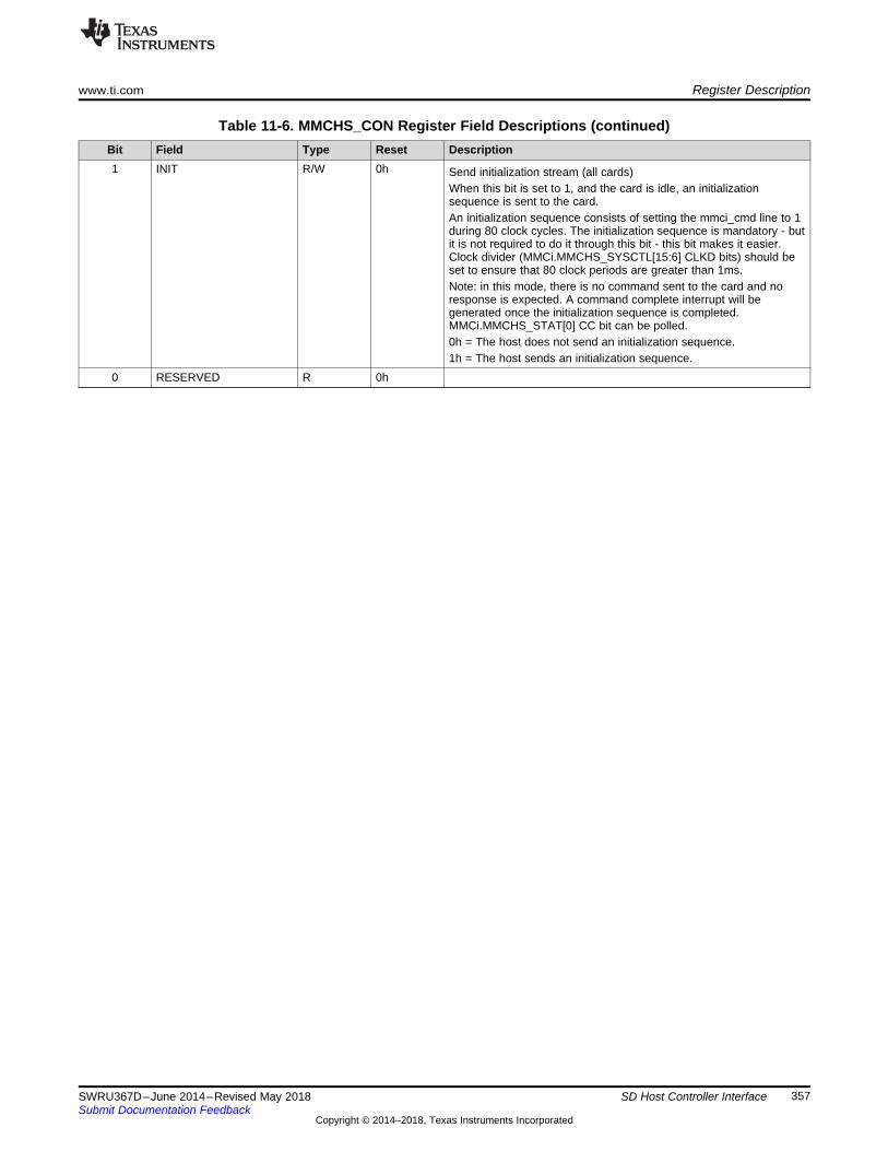
www.ti.com Register Description
357SWRU367D–June 2014–Revised May 2018Submit Documentation Feedback
Copyright © 2014–2018, Texas Instruments Incorporated
SD Host Controller Interface
Table 11-6. MMCHS_CON Register Field Descriptions (continued)Bit Field Type Reset Description1 INIT R/W 0h Send initialization stream (all cards)
When this bit is set to 1, and the card is idle, an initializationsequence is sent to the card.An initialization sequence consists of setting the mmci_cmd line to 1during 80 clock cycles. The initialization sequence is mandatory - butit is not required to do it through this bit - this bit makes it easier.Clock divider (MMCi.MMCHS_SYSCTL[15:6] CLKD bits) should beset to ensure that 80 clock periods are greater than 1ms.Note: in this mode, there is no command sent to the card and noresponse is expected. A command complete interrupt will begenerated once the initialization sequence is completed.MMCi.MMCHS_STAT[0] CC bit can be polled.0h = The host does not send an initialization sequence.1h = The host sends an initialization sequence.
0 RESERVED R 0h
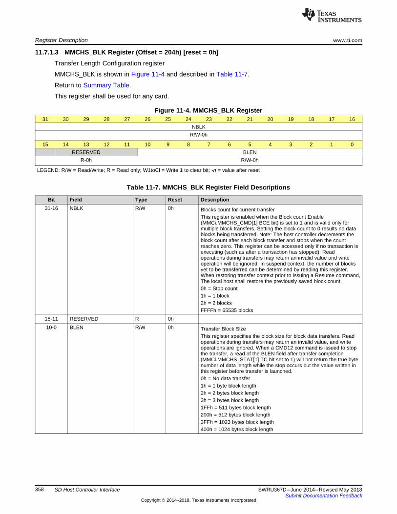
Register Description www.ti.com
358 SWRU367D–June 2014–Revised May 2018Submit Documentation Feedback
Copyright © 2014–2018, Texas Instruments Incorporated
SD Host Controller Interface
11.7.1.3 MMCHS_BLK Register (Offset = 204h) [reset = 0h]Transfer Length Configuration register
MMCHS_BLK is shown in Figure 11-4 and described in Table 11-7.
Return to Summary Table.
This register shall be used for any card.
Figure 11-4. MMCHS_BLK Register31 30 29 28 27 26 25 24 23 22 21 20 19 18 17 16
NBLKR/W-0h
15 14 13 12 11 10 9 8 7 6 5 4 3 2 1 0RESERVED BLEN
R-0h R/W-0h
LEGEND: R/W = Read/Write; R = Read only; W1toCl = Write 1 to clear bit; -n = value after reset
Table 11-7. MMCHS_BLK Register Field Descriptions
Bit Field Type Reset Description31-16 NBLK R/W 0h Blocks count for current transfer
This register is enabled when the Block count Enable(MMCi.MMCHS_CMD[1] BCE bit) is set to 1 and is valid only formultiple block transfers. Setting the block count to 0 results no datablocks being transferred. Note: The host controller decrements theblock count after each block transfer and stops when the countreaches zero. This register can be accessed only if no transaction isexecuting (such as after a transaction has stopped). Readoperations during transfers may return an invalid value and writeoperation will be ignored. In suspend context, the number of blocksyet to be transferred can be determined by reading this register.When restoring transfer context prior to issuing a Resume command,The local host shall restore the previously saved block count.0h = Stop count1h = 1 block2h = 2 blocksFFFFh = 65535 blocks
15-11 RESERVED R 0h10-0 BLEN R/W 0h Transfer Block Size
This register specifies the block size for block data transfers. Readoperations during transfers may return an invalid value, and writeoperations are ignored. When a CMD12 command is issued to stopthe transfer, a read of the BLEN field after transfer completion(MMCi.MMCHS_STAT[1] TC bit set to 1) will not return the true bytenumber of data length while the stop occurs but the value written inthis register before transfer is launched.0h = No data transfer1h = 1 byte block length2h = 2 bytes block length3h = 3 bytes block length1FFh = 511 bytes block length200h = 512 bytes block length3FFh = 1023 bytes block length400h = 1024 bytes block length
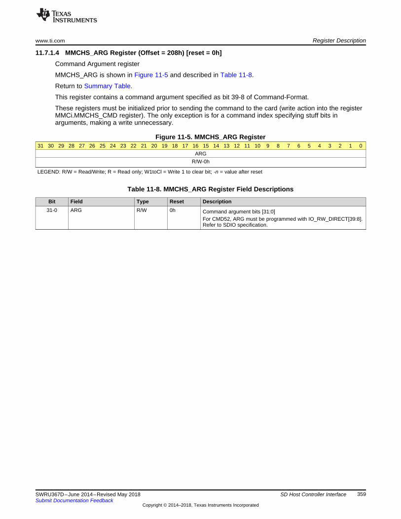
www.ti.com Register Description
359SWRU367D–June 2014–Revised May 2018Submit Documentation Feedback
Copyright © 2014–2018, Texas Instruments Incorporated
SD Host Controller Interface
11.7.1.4 MMCHS_ARG Register (Offset = 208h) [reset = 0h]Command Argument register
MMCHS_ARG is shown in Figure 11-5 and described in Table 11-8.
Return to Summary Table.
This register contains a command argument specified as bit 39-8 of Command-Format.
These registers must be initialized prior to sending the command to the card (write action into the registerMMCi.MMCHS_CMD register). The only exception is for a command index specifying stuff bits inarguments, making a write unnecessary.
Figure 11-5. MMCHS_ARG Register31 30 29 28 27 26 25 24 23 22 21 20 19 18 17 16 15 14 13 12 11 10 9 8 7 6 5 4 3 2 1 0
ARGR/W-0h
LEGEND: R/W = Read/Write; R = Read only; W1toCl = Write 1 to clear bit; -n = value after reset
Table 11-8. MMCHS_ARG Register Field Descriptions
Bit Field Type Reset Description31-0 ARG R/W 0h Command argument bits [31:0]
For CMD52, ARG must be programmed with IO_RW_DIRECT[39:8].Refer to SDIO specification.
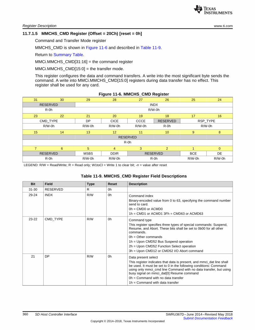
Register Description www.ti.com
360 SWRU367D–June 2014–Revised May 2018Submit Documentation Feedback
Copyright © 2014–2018, Texas Instruments Incorporated
SD Host Controller Interface
11.7.1.5 MMCHS_CMD Register (Offset = 20Ch) [reset = 0h]Command and Transfer Mode register
MMCHS_CMD is shown in Figure 11-6 and described in Table 11-9.
Return to Summary Table.
MMCi.MMCHS_CMD[31:16] = the command register
MMCi.MMCHS_CMD[15:0] = the transfer mode.
This register configures the data and command transfers. A write into the most significant byte sends thecommand. A write into MMCi.MMCHS_CMD[15:0] registers during data transfer has no effect. Thisregister shall be used for any card.
Figure 11-6. MMCHS_CMD Register31 30 29 28 27 26 25 24
RESERVED INDXR-0h R/W-0h
23 22 21 20 19 18 17 16CMD_TYPE DP CICE CCCE RESERVED RSP_TYPE
R/W-0h R/W-0h R/W-0h R/W-0h R-0h R/W-0h
15 14 13 12 11 10 9 8RESERVED
R-0h
7 6 5 4 3 2 1 0RESERVED MSBS DDIR RESERVED BCE DE
R-0h R/W-0h R/W-0h R-0h R/W-0h R/W-0h
LEGEND: R/W = Read/Write; R = Read only; W1toCl = Write 1 to clear bit; -n = value after reset
Table 11-9. MMCHS_CMD Register Field Descriptions
Bit Field Type Reset Description31-30 RESERVED R 0h29-24 INDX R/W 0h Command index
Binary-encoded value from 0 to 63, specifying the command numbersend to card.0h = CMD0 or ACMD01h = CMD1 or ACMD1 3Fh = CMD63 or ACMD63
23-22 CMD_TYPE R/W 0h Command typeThis register specifies three types of special commands: Suspend,Resume, and Abort. These bits shall be set to 0b00 for all othercommands.0h = Other commands1h = Upon CMD52 Bus Suspend operation2h = Upon CMD52 Function Select operation3h = Upon CMD12 or CMD52 I/O Abort command
21 DP R/W 0h Data present selectThis register indicates that data is present, and mmci_dat line shallbe used. It must be set to 0 in the following conditions: Commandusing only mmci_cmd line Command with no data transfer, but usingbusy signal on mmci_dat[0] Resume command0h = Command with no data transfer1h = Command with data transfer
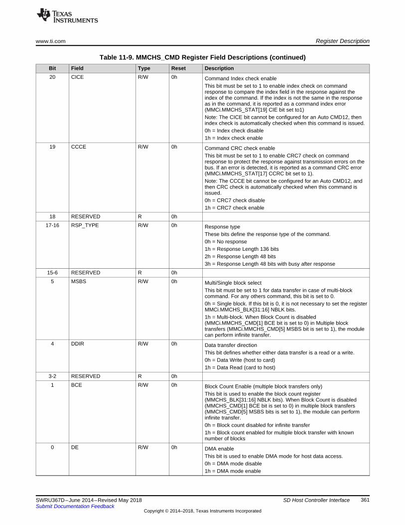
www.ti.com Register Description
361SWRU367D–June 2014–Revised May 2018Submit Documentation Feedback
Copyright © 2014–2018, Texas Instruments Incorporated
SD Host Controller Interface
Table 11-9. MMCHS_CMD Register Field Descriptions (continued)Bit Field Type Reset Description20 CICE R/W 0h Command Index check enable
This bit must be set to 1 to enable index check on commandresponse to compare the index field in the response against theindex of the command. If the index is not the same in the responseas in the command, it is reported as a command index error(MMCi.MMCHS_STAT[19] CIE bit set to1)Note: The CICE bit cannot be configured for an Auto CMD12, thenindex check is automatically checked when this command is issued.0h = Index check disable1h = Index check enable
19 CCCE R/W 0h Command CRC check enableThis bit must be set to 1 to enable CRC7 check on commandresponse to protect the response against transmission errors on thebus. If an error is detected, it is reported as a command CRC error(MMCi.MMCHS_STAT[17] CCRC bit set to 1).Note: The CCCE bit cannot be configured for an Auto CMD12, andthen CRC check is automatically checked when this command isissued.0h = CRC7 check disable1h = CRC7 check enable
18 RESERVED R 0h17-16 RSP_TYPE R/W 0h Response type
These bits define the response type of the command.0h = No response1h = Response Length 136 bits2h = Response Length 48 bits3h = Response Length 48 bits with busy after response
15-6 RESERVED R 0h5 MSBS R/W 0h Multi/Single block select
This bit must be set to 1 for data transfer in case of multi-blockcommand. For any others command, this bit is set to 0.0h = Single block. If this bit is 0, it is not necessary to set the registerMMCi.MMCHS_BLK[31:16] NBLK bits.1h = Multi-block. When Block Count is disabled(MMCi.MMCHS_CMD[1] BCE bit is set to 0) in Multiple blocktransfers (MMCi.MMCHS_CMD[5] MSBS bit is set to 1), the modulecan perform infinite transfer.
4 DDIR R/W 0h Data transfer directionThis bit defines whether either data transfer is a read or a write.0h = Data Write (host to card)1h = Data Read (card to host)
3-2 RESERVED R 0h1 BCE R/W 0h Block Count Enable (multiple block transfers only)
This bit is used to enable the block count register(MMCHS_BLK[31:16] NBLK bits). When Block Count is disabled(MMCHS_CMD[1] BCE bit is set to 0) in multiple block transfers(MMCHS_CMD[5] MSBS bits is set to 1), the module can performinfinite transfer.0h = Block count disabled for infinite transfer1h = Block count enabled for multiple block transfer with knownnumber of blocks
0 DE R/W 0h DMA enableThis bit is used to enable DMA mode for host data access.0h = DMA mode disable1h = DMA mode enable
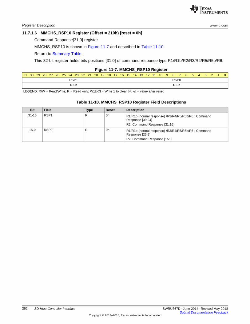
Register Description www.ti.com
362 SWRU367D–June 2014–Revised May 2018Submit Documentation Feedback
Copyright © 2014–2018, Texas Instruments Incorporated
SD Host Controller Interface
11.7.1.6 MMCHS_RSP10 Register (Offset = 210h) [reset = 0h]Command Response[31:0] register
MMCHS_RSP10 is shown in Figure 11-7 and described in Table 11-10.
Return to Summary Table.
This 32-bit register holds bits positions [31:0] of command response type R1/R1b/R2/R3/R4/R5/R5b/R6.
Figure 11-7. MMCHS_RSP10 Register31 30 29 28 27 26 25 24 23 22 21 20 19 18 17 16 15 14 13 12 11 10 9 8 7 6 5 4 3 2 1 0
RSP1 RSP0R-0h R-0h
LEGEND: R/W = Read/Write; R = Read only; W1toCl = Write 1 to clear bit; -n = value after reset
Table 11-10. MMCHS_RSP10 Register Field Descriptions
Bit Field Type Reset Description31-16 RSP1 R 0h R1/R1b (normal response) /R3/R4/R5/R5b/R6 : Command
Response [39:24]R2: Command Response [31:16]
15-0 RSP0 R 0h R1/R1b (normal response) /R3/R4/R5/R5b/R6 : CommandResponse [23:8]R2: Command Response [15:0]
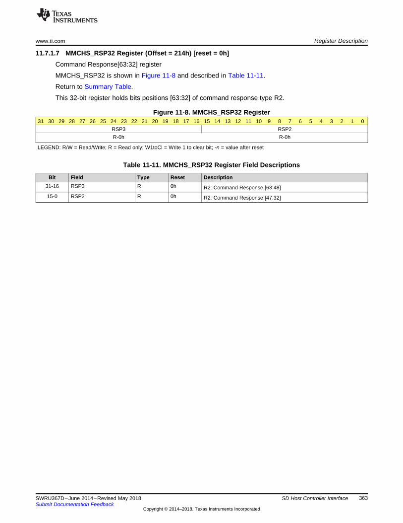
www.ti.com Register Description
363SWRU367D–June 2014–Revised May 2018Submit Documentation Feedback
Copyright © 2014–2018, Texas Instruments Incorporated
SD Host Controller Interface
11.7.1.7 MMCHS_RSP32 Register (Offset = 214h) [reset = 0h]Command Response[63:32] register
MMCHS_RSP32 is shown in Figure 11-8 and described in Table 11-11.
Return to Summary Table.
This 32-bit register holds bits positions [63:32] of command response type R2.
Figure 11-8. MMCHS_RSP32 Register31 30 29 28 27 26 25 24 23 22 21 20 19 18 17 16 15 14 13 12 11 10 9 8 7 6 5 4 3 2 1 0
RSP3 RSP2R-0h R-0h
LEGEND: R/W = Read/Write; R = Read only; W1toCl = Write 1 to clear bit; -n = value after reset
Table 11-11. MMCHS_RSP32 Register Field Descriptions
Bit Field Type Reset Description31-16 RSP3 R 0h R2: Command Response [63:48]15-0 RSP2 R 0h R2: Command Response [47:32]
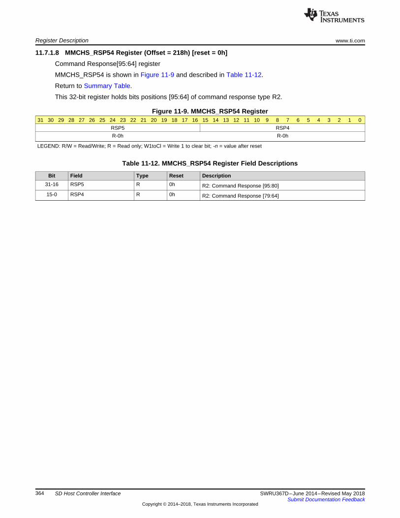
Register Description www.ti.com
364 SWRU367D–June 2014–Revised May 2018Submit Documentation Feedback
Copyright © 2014–2018, Texas Instruments Incorporated
SD Host Controller Interface
11.7.1.8 MMCHS_RSP54 Register (Offset = 218h) [reset = 0h]Command Response[95:64] register
MMCHS_RSP54 is shown in Figure 11-9 and described in Table 11-12.
Return to Summary Table.
This 32-bit register holds bits positions [95:64] of command response type R2.
Figure 11-9. MMCHS_RSP54 Register31 30 29 28 27 26 25 24 23 22 21 20 19 18 17 16 15 14 13 12 11 10 9 8 7 6 5 4 3 2 1 0
RSP5 RSP4R-0h R-0h
LEGEND: R/W = Read/Write; R = Read only; W1toCl = Write 1 to clear bit; -n = value after reset
Table 11-12. MMCHS_RSP54 Register Field Descriptions
Bit Field Type Reset Description31-16 RSP5 R 0h R2: Command Response [95:80]15-0 RSP4 R 0h R2: Command Response [79:64]

www.ti.com Register Description
365SWRU367D–June 2014–Revised May 2018Submit Documentation Feedback
Copyright © 2014–2018, Texas Instruments Incorporated
SD Host Controller Interface
11.7.1.9 MMCHS_RSP76 Register (Offset = 21Ch) [reset = 0h]Command Response[127:96] register
MMCHS_RSP76 is shown in Figure 11-10 and described in Table 11-13.
Return to Summary Table.
This 32-bit register holds bits positions [127:96] of command response type R2.
Figure 11-10. MMCHS_RSP76 Register31 30 29 28 27 26 25 24 23 22 21 20 19 18 17 16 15 14 13 12 11 10 9 8 7 6 5 4 3 2 1 0
RSP7 RSP6R-0h R-0h
LEGEND: R/W = Read/Write; R = Read only; W1toCl = Write 1 to clear bit; -n = value after reset
Table 11-13. MMCHS_RSP76 Register Field Descriptions
Bit Field Type Reset Description31-16 RSP7 R 0h R1b (Auto CMD12 response): Command Response [39:24]
R2: Command Response [127:112]15-0 RSP6 R 0h R1b (Auto CMD12 response): Command Response [23:8]
R2: Command Response [111:96]
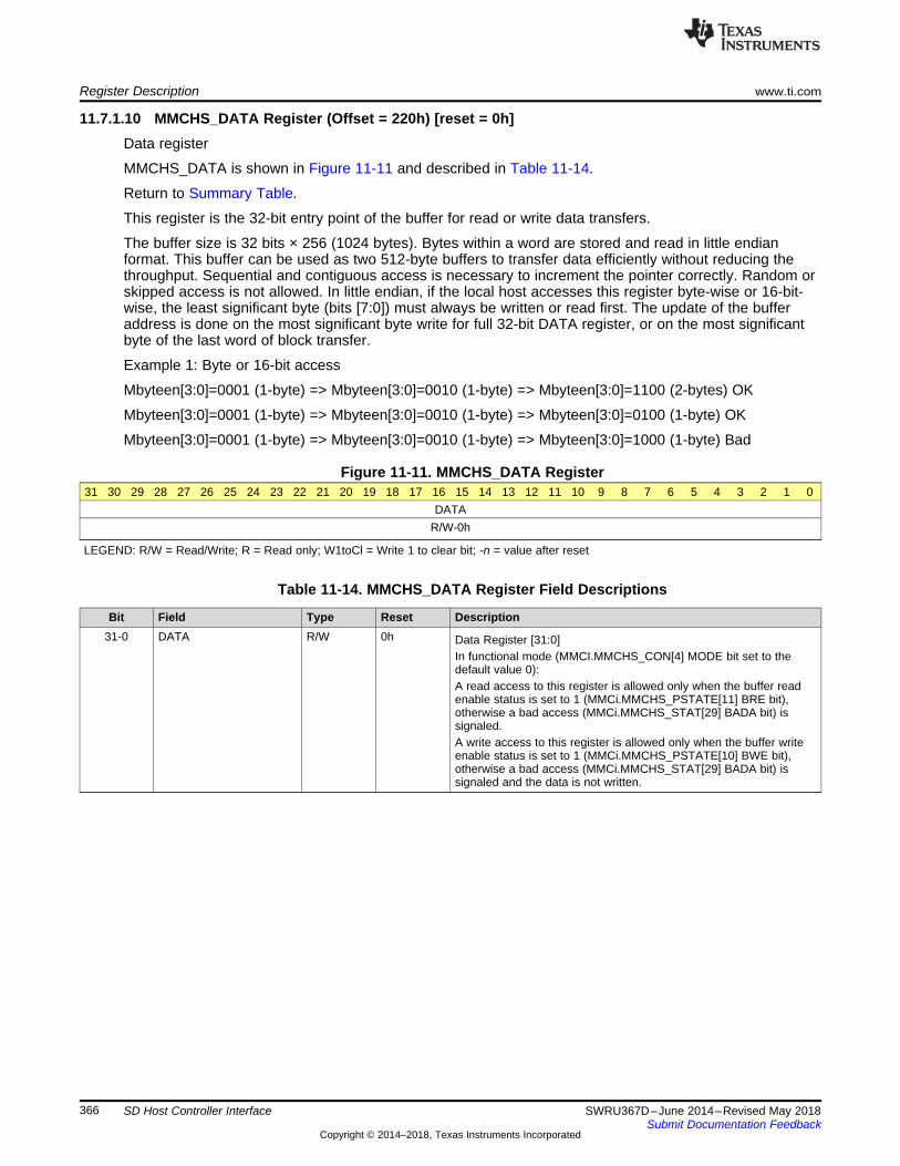
Register Description www.ti.com
366 SWRU367D–June 2014–Revised May 2018Submit Documentation Feedback
Copyright © 2014–2018, Texas Instruments Incorporated
SD Host Controller Interface
11.7.1.10 MMCHS_DATA Register (Offset = 220h) [reset = 0h]Data register
MMCHS_DATA is shown in Figure 11-11 and described in Table 11-14.
Return to Summary Table.
This register is the 32-bit entry point of the buffer for read or write data transfers.
The buffer size is 32 bits × 256 (1024 bytes). Bytes within a word are stored and read in little endianformat. This buffer can be used as two 512-byte buffers to transfer data efficiently without reducing thethroughput. Sequential and contiguous access is necessary to increment the pointer correctly. Random orskipped access is not allowed. In little endian, if the local host accesses this register byte-wise or 16-bit-wise, the least significant byte (bits [7:0]) must always be written or read first. The update of the bufferaddress is done on the most significant byte write for full 32-bit DATA register, or on the most significantbyte of the last word of block transfer.
Example 1: Byte or 16-bit access
Mbyteen[3:0]=0001 (1-byte) => Mbyteen[3:0]=0010 (1-byte) => Mbyteen[3:0]=1100 (2-bytes) OK
Mbyteen[3:0]=0001 (1-byte) => Mbyteen[3:0]=0010 (1-byte) => Mbyteen[3:0]=0100 (1-byte) OK
Mbyteen[3:0]=0001 (1-byte) => Mbyteen[3:0]=0010 (1-byte) => Mbyteen[3:0]=1000 (1-byte) Bad
Figure 11-11. MMCHS_DATA Register31 30 29 28 27 26 25 24 23 22 21 20 19 18 17 16 15 14 13 12 11 10 9 8 7 6 5 4 3 2 1 0
DATAR/W-0h
LEGEND: R/W = Read/Write; R = Read only; W1toCl = Write 1 to clear bit; -n = value after reset
Table 11-14. MMCHS_DATA Register Field Descriptions
Bit Field Type Reset Description31-0 DATA R/W 0h Data Register [31:0]
In functional mode (MMCI.MMCHS_CON[4] MODE bit set to thedefault value 0):A read access to this register is allowed only when the buffer readenable status is set to 1 (MMCi.MMCHS_PSTATE[11] BRE bit),otherwise a bad access (MMCi.MMCHS_STAT[29] BADA bit) issignaled.A write access to this register is allowed only when the buffer writeenable status is set to 1 (MMCi.MMCHS_PSTATE[10] BWE bit),otherwise a bad access (MMCi.MMCHS_STAT[29] BADA bit) issignaled and the data is not written.
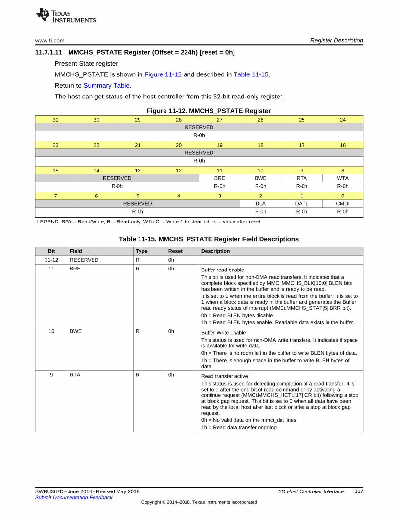
www.ti.com Register Description
367SWRU367D–June 2014–Revised May 2018Submit Documentation Feedback
Copyright © 2014–2018, Texas Instruments Incorporated
SD Host Controller Interface
11.7.1.11 MMCHS_PSTATE Register (Offset = 224h) [reset = 0h]Present State register
MMCHS_PSTATE is shown in Figure 11-12 and described in Table 11-15.
Return to Summary Table.
The host can get status of the host controller from this 32-bit read-only register.
Figure 11-12. MMCHS_PSTATE Register31 30 29 28 27 26 25 24
RESERVEDR-0h
23 22 21 20 19 18 17 16RESERVED
R-0h
15 14 13 12 11 10 9 8RESERVED BRE BWE RTA WTA
R-0h R-0h R-0h R-0h R-0h
7 6 5 4 3 2 1 0RESERVED DLA DAT1 CMDI
R-0h R-0h R-0h R-0h
LEGEND: R/W = Read/Write; R = Read only; W1toCl = Write 1 to clear bit; -n = value after reset
Table 11-15. MMCHS_PSTATE Register Field Descriptions
Bit Field Type Reset Description31-12 RESERVED R 0h
11 BRE R 0h Buffer read enableThis bit is used for non-DMA read transfers. It indicates that acomplete block specified by MMCi.MMCHS_BLK[10:0] BLEN bitshas been written in the buffer and is ready to be read.It is set to 0 when the entire block is read from the buffer. It is set to1 when a block data is ready in the buffer and generates the Bufferread ready status of interrupt (MMCi.MMCHS_STAT[5] BRR bit).0h = Read BLEN bytes disable1h = Read BLEN bytes enable. Readable data exists in the buffer.
10 BWE R 0h Buffer Write enableThis status is used for non-DMA write transfers. It indicates if spaceis available for write data.0h = There is no room left in the buffer to write BLEN bytes of data.1h = There is enough space in the buffer to write BLEN bytes ofdata.
9 RTA R 0h Read transfer activeThis status is used for detecting completion of a read transfer. It isset to 1 after the end bit of read command or by activating acontinue request (MMCi.MMCHS_HCTL[17] CR bit) following a stopat block gap request. This bit is set to 0 when all data have beenread by the local host after last block or after a stop at block gaprequest.0h = No valid data on the mmci_dat lines1h = Read data transfer ongoing
Register Description www.ti.com
368 SWRU367D–June 2014–Revised May 2018Submit Documentation Feedback
Copyright © 2014–2018, Texas Instruments Incorporated
SD Host Controller Interface
Table 11-15. MMCHS_PSTATE Register Field Descriptions (continued)Bit Field Type Reset Description8 WTA R 0h Write transfer active
This status indicates a write transfer active. It is set to 1 after the endbit of write command or by activating a continue request(MMCi.MMCHS_HCTL[17] CR bit) following a stop at block gaprequest. This bit is set to 0 when CRC status has been received afterlast block or after a stop at block gap request.0h = No valid data on the mmci_dat lines1h = Write data transfer ongoing
7-3 RESERVED R 0h2 DLA R 0h mmci_dat line active
This status bit indicates whether one of the mmci_dat line is in use.In the case of read transactions (card to host):This bit is set to 1 after the end bit of read command or by activatingcontinue request MMCi.MMCHS_HCTL[17] CR bit.This bit is set to 0 when the host controller received the end bit ofthe last data block or at the beginning of the read wait mode. In thecase of write transactions (host to card):This bit is set to 1 after the end bit of write command or by activatingcontinue request MMCi.MMCHS_HCTL[17] CR bit.This bit is set to 0 on the end of busy event for the last block; hostcontroller must wait 8 clock cycles with line not busy to reallyconsider not "busy state" or after the busy block as a result of a stopat gap request.0h = mmci_dat Line inactive1h = mmci_dat Line active
1 DAT1 R 0h Command inhibit (mmci_dat)This status bit is generated if either mmci_dat line is active(MMCi.MMCHS_PSTATE[2] DLA bit) or Read transfer is active(MMCi.MMCHS_PSTATE[9] RTA bit) or when a command with busyis issued.This bit prevents the local host to issue a command.A change of this bit from 1 to 0 generates a transfer completeinterrupt (MMCi.MMCHS_STAT[1] TC bit).0h = Issuing of command using the mmci_dat lines is allowed1h = Issuing of command using the mmci_dat lines is not allowed
0 CMDI R 0h Command inhibit(mmci_cmd)This status bit indicates that the mmci_cmd line is in use. This bit isset to 0 when the most significant byte is written into the commandregister. This bit is not set when Auto CMD12 is transmitted. This bitis set to 0 in either the following cases:After the end bit of the command response, excepted if there is acommand conflict error (MMCi.MMCHS_STAT[17] CCRC bit orMMCi.MMCHS_STAT[18] CEB bit set to 1) or a Auto CMD12 is notexecuted (MMCi.MMCHS_AC12[0] ACNE bit).After the end bit of the command without response(MMCi.MMCHS_CMD[17:16] RSP_TYPE bits set to "00"). In case ofa command data error is detected (MMCi.MMCHS_STAT[19] CTObit set to 1), this register is not automatically cleared.0h = Issuing of command using mmci_cmd line is allowed1h = Issuing of command using mmci_cmd line is not allowed
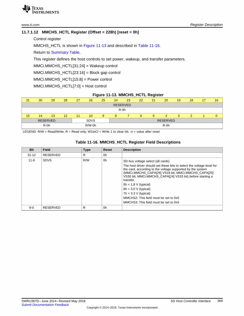
www.ti.com Register Description
369SWRU367D–June 2014–Revised May 2018Submit Documentation Feedback
Copyright © 2014–2018, Texas Instruments Incorporated
SD Host Controller Interface
11.7.1.12 MMCHS_HCTL Register (Offset = 228h) [reset = 0h]Control register
MMCHS_HCTL is shown in Figure 11-13 and described in Table 11-16.
Return to Summary Table.
This register defines the host controls to set power, wakeup, and transfer parameters.
MMCi.MMCHS_HCTL[31:24] = Wakeup control
MMCi.MMCHS_HCTL[23:16] = Block gap control
MMCi.MMCHS_HCTL[15:8] = Power control
MMCi.MMCHS_HCTL[7:0] = Host control
Figure 11-13. MMCHS_HCTL Register31 30 29 28 27 26 25 24 23 22 21 20 19 18 17 16
RESERVEDR-0h
15 14 13 12 11 10 9 8 7 6 5 4 3 2 1 0RESERVED SDVS RESERVED
R-0h R/W-0h R-0h
LEGEND: R/W = Read/Write; R = Read only; W1toCl = Write 1 to clear bit; -n = value after reset
Table 11-16. MMCHS_HCTL Register Field Descriptions
Bit Field Type Reset Description31-12 RESERVED R 0h11-9 SDVS R/W 0h SD bus voltage select (all cards)
The host driver should set these bits to select the voltage level forthe card, according to the voltage supported by the system(MMCi.MMCHS_CAPA[26] VS18 bit, MMCi.MMCHS_CAPA[25]VS30 bit, MMCi.MMCHS_CAPA[24] VS33 bit) before starting atransfer.5h = 1.8 V (typical)6h = 3.0 V (typical)7h = 3.3 V (typical)MMCHS2: This field must be set to 0x5MMCHS3: This field must be set to 0x5
8-0 RESERVED R 0h

Register Description www.ti.com
370 SWRU367D–June 2014–Revised May 2018Submit Documentation Feedback
Copyright © 2014–2018, Texas Instruments Incorporated
SD Host Controller Interface
11.7.1.13 MMCHS_SYSCTL Register (Offset = 22Ch) [reset = 0h]SD System Control register
MMCHS_SYSCTL is shown in Figure 11-14 and described in Table 11-17.
Return to Summary Table.
This register defines the system controls to set software resets, clock frequency management, and datatime-out.
MMCHS_SYSCTL[31:24] = Software resets
MMCHS_SYSCTL[23:16] = Timeout control
MMCHS_SYSCTL[15:0] = Clock control
Figure 11-14. MMCHS_SYSCTL Register31 30 29 28 27 26 25 24 23 22 21 20 19 18 17 16
RESERVED SRD SRC SRA RESERVED DTOR-0h R/W-
0hR/W-
0hR/W-
0hR-0h R/W-0h
15 14 13 12 11 10 9 8 7 6 5 4 3 2 1 0CLKD RESERVED CEN ICS ICE
R/W-0h R-0h R/W-0h
R-0h R/W-0h
LEGEND: R/W = Read/Write; R = Read only; W1toCl = Write 1 to clear bit; -n = value after reset
Table 11-17. MMCHS_SYSCTL Register Field Descriptions
Bit Field Type Reset Description31-27 RESERVED R 0h
26 SRD R/W 0h Software reset for mmci_dat lineThis bit is set to 1 for reset and released to 0 when completed.mmci_dat finite state machine in both clock domain are also reset.These registers are cleared by the MMCHS_SYSCTL[26] SRD bit:MMCi.MMCHS_DATA MMCi.MMCHS_PSTATE: BRE, BWE, RTA,WTA, DLA and DATIMMCi.MMCHS_HCTL: SBGR and CRMMCi.MMCHS_STAT: BRR, BWR, BGE and TC Interconnect andMMC buffer data management is reinitialized.0h = Reset completed1h = Software reset for mmci_dat line
25 SRC R/W 0h Software reset for mmci_cmd lineThis bit is set to 1 for reset and released to 0 when completed.mmci_cmd finite state machine in both clock domain are also reset.These are the registers cleared by the MMCi.MMCHS_SYSCTL[25]SRC bit:MMCi.MMCHS_PSTATE: CMDIMMCi.MMCHS_STAT: CC Interconnect and MMC command statusmanagement is reinitialized.0h = Reset completed1h = Software reset for mmci_dat line
24 SRA R/W 0h Software reset for allThis bit is set to 1 for reset , and released to 0 when RW 0completed. This reset affects the entire host controller except for thecard detection circuit and capabilities registers.0h = Reset completed1h = Software reset for all the designs
23-20 RESERVED R 0h
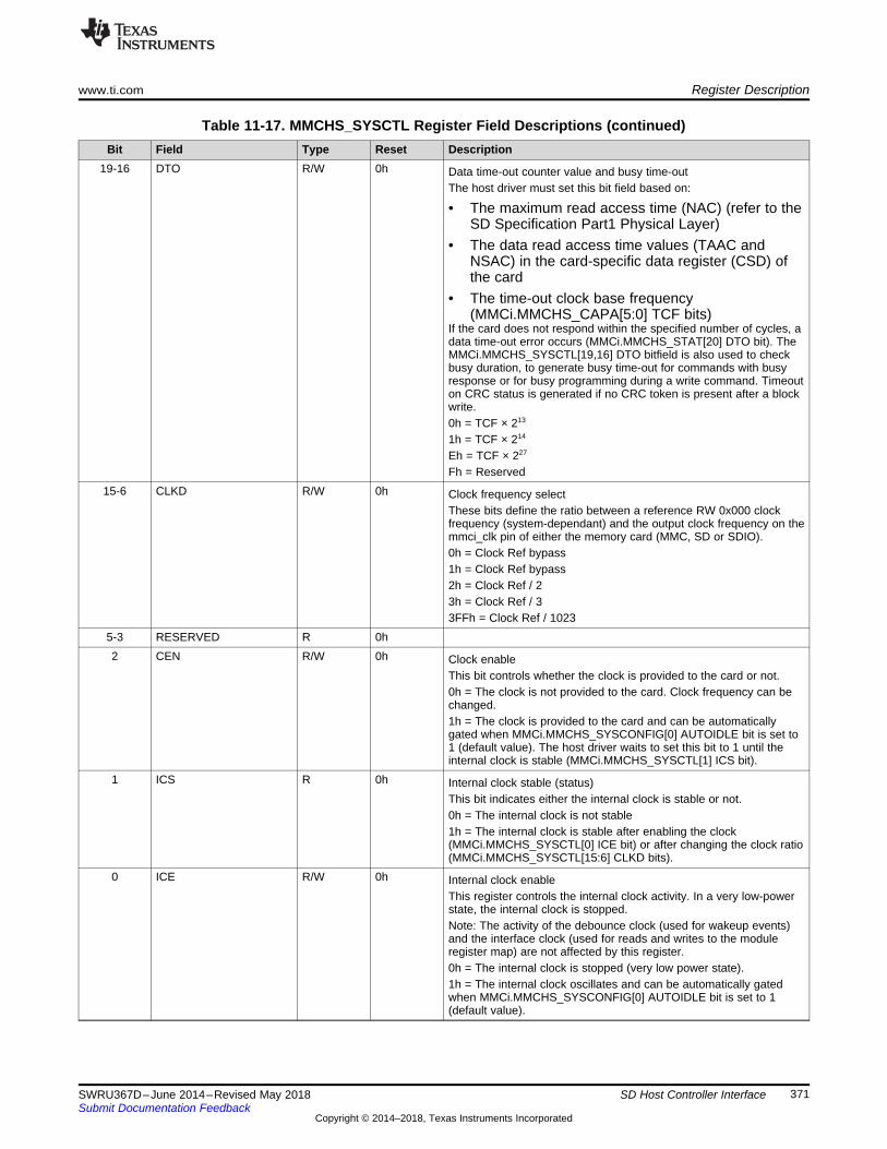
www.ti.com Register Description
371SWRU367D–June 2014–Revised May 2018Submit Documentation Feedback
Copyright © 2014–2018, Texas Instruments Incorporated
SD Host Controller Interface
Table 11-17. MMCHS_SYSCTL Register Field Descriptions (continued)Bit Field Type Reset Description
19-16 DTO R/W 0h Data time-out counter value and busy time-outThe host driver must set this bit field based on:
• The maximum read access time (NAC) (refer to theSD Specification Part1 Physical Layer)
• The data read access time values (TAAC andNSAC) in the card-specific data register (CSD) ofthe card
• The time-out clock base frequency(MMCi.MMCHS_CAPA[5:0] TCF bits)
If the card does not respond within the specified number of cycles, adata time-out error occurs (MMCi.MMCHS_STAT[20] DTO bit). TheMMCi.MMCHS_SYSCTL[19,16] DTO bitfield is also used to checkbusy duration, to generate busy time-out for commands with busyresponse or for busy programming during a write command. Timeouton CRC status is generated if no CRC token is present after a blockwrite.0h = TCF × 213
1h = TCF × 214
Eh = TCF × 227
Fh = Reserved15-6 CLKD R/W 0h Clock frequency select
These bits define the ratio between a reference RW 0x000 clockfrequency (system-dependant) and the output clock frequency on themmci_clk pin of either the memory card (MMC, SD or SDIO).0h = Clock Ref bypass1h = Clock Ref bypass2h = Clock Ref / 23h = Clock Ref / 33FFh = Clock Ref / 1023
5-3 RESERVED R 0h2 CEN R/W 0h Clock enable
This bit controls whether the clock is provided to the card or not.0h = The clock is not provided to the card. Clock frequency can bechanged.1h = The clock is provided to the card and can be automaticallygated when MMCi.MMCHS_SYSCONFIG[0] AUTOIDLE bit is set to1 (default value). The host driver waits to set this bit to 1 until theinternal clock is stable (MMCi.MMCHS_SYSCTL[1] ICS bit).
1 ICS R 0h Internal clock stable (status)This bit indicates either the internal clock is stable or not.0h = The internal clock is not stable1h = The internal clock is stable after enabling the clock(MMCi.MMCHS_SYSCTL[0] ICE bit) or after changing the clock ratio(MMCi.MMCHS_SYSCTL[15:6] CLKD bits).
0 ICE R/W 0h Internal clock enableThis register controls the internal clock activity. In a very low-powerstate, the internal clock is stopped.Note: The activity of the debounce clock (used for wakeup events)and the interface clock (used for reads and writes to the moduleregister map) are not affected by this register.0h = The internal clock is stopped (very low power state).1h = The internal clock oscillates and can be automatically gatedwhen MMCi.MMCHS_SYSCONFIG[0] AUTOIDLE bit is set to 1(default value).
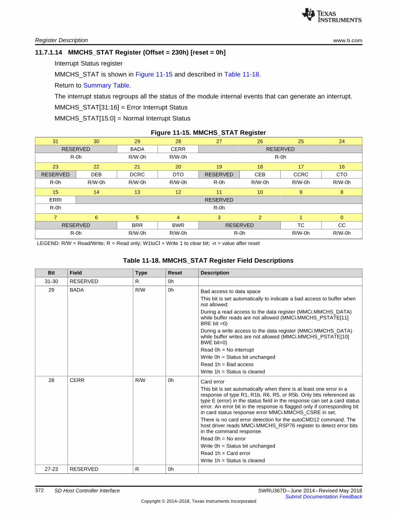
Register Description www.ti.com
372 SWRU367D–June 2014–Revised May 2018Submit Documentation Feedback
Copyright © 2014–2018, Texas Instruments Incorporated
SD Host Controller Interface
11.7.1.14 MMCHS_STAT Register (Offset = 230h) [reset = 0h]Interrupt Status register
MMCHS_STAT is shown in Figure 11-15 and described in Table 11-18.
Return to Summary Table.
The interrupt status regroups all the status of the module internal events that can generate an interrupt.
MMCHS_STAT[31:16] = Error Interrupt Status
MMCHS_STAT[15:0] = Normal Interrupt Status
Figure 11-15. MMCHS_STAT Register31 30 29 28 27 26 25 24
RESERVED BADA CERR RESERVEDR-0h R/W-0h R/W-0h R-0h
23 22 21 20 19 18 17 16RESERVED DEB DCRC DTO RESERVED CEB CCRC CTO
R-0h R/W-0h R/W-0h R/W-0h R-0h R/W-0h R/W-0h R/W-0h
15 14 13 12 11 10 9 8ERRI RESERVEDR-0h R-0h
7 6 5 4 3 2 1 0RESERVED BRR BWR RESERVED TC CC
R-0h R/W-0h R/W-0h R-0h R/W-0h R/W-0h
LEGEND: R/W = Read/Write; R = Read only; W1toCl = Write 1 to clear bit; -n = value after reset
Table 11-18. MMCHS_STAT Register Field Descriptions
Bit Field Type Reset Description31-30 RESERVED R 0h
29 BADA R/W 0h Bad access to data spaceThis bit is set automatically to indicate a bad access to buffer whennot allowed:During a read access to the data register (MMCi.MMCHS_DATA)while buffer reads are not allowed (MMCi.MMCHS_PSTATE[11]BRE bit =0)During a write access to the data register (MMCi.MMCHS_DATA)while buffer writes are not allowed (MMCi.MMCHS_PSTATE[10]BWE bit=0)Read 0h = No interruptWrite 0h = Status bit unchangedRead 1h = Bad accessWrite 1h = Status is cleared
28 CERR R/W 0h Card errorThis bit is set automatically when there is at least one error in aresponse of type R1, R1b, R6, R5, or R5b. Only bits referenced astype E (error) in the status field in the response can set a card statuserror. An error bit in the response is flagged only if corresponding bitin card status response error MMCi.MMCHS_CSRE in set.There is no card error detection for the autoCMD12 command. Thehost driver reads MMCi.MMCHS_RSP76 register to detect error bitsin the command response.Read 0h = No errorWrite 0h = Status bit unchangedRead 1h = Card errorWrite 1h = Status is cleared
27-23 RESERVED R 0h
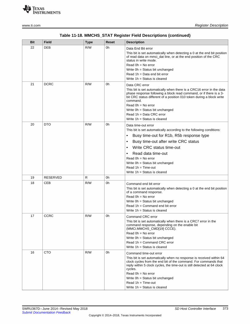
www.ti.com Register Description
373SWRU367D–June 2014–Revised May 2018Submit Documentation Feedback
Copyright © 2014–2018, Texas Instruments Incorporated
SD Host Controller Interface
Table 11-18. MMCHS_STAT Register Field Descriptions (continued)Bit Field Type Reset Description22 DEB R/W 0h Data End Bit error
This bit is set automatically when detecting a 0 at the end bit positionof read data on mmci_dat line, or at the end position of the CRCstatus in write mode.Read 0h = No errorWrite 0h = Status bit unchangedRead 1h = Data end bit errorWrite 1h = Status is cleared
21 DCRC R/W 0h Data CRC errorThis bit is set automatically when there is a CRC16 error in the dataphase response following a block read command, or if there is a 3-bit CRC status different of a position 010 token during a block writecommand.Read 0h = No errorWrite 0h = Status bit unchangedRead 1h = Data CRC errorWrite 1h = Status is cleared
20 DTO R/W 0h Data time-out errorThis bit is set automatically according to the following conditions:
• Busy time-out for R1b, R5b response type• Busy time-out after write CRC status• Write CRC status time-out• Read data time-outRead 0h = No errorWrite 0h = Status bit unchangedRead 1h = Time-outWrite 1h = Status is cleared
19 RESERVED R 0h18 CEB R/W 0h Command end bit error
This bit is set automatically when detecting a 0 at the end bit positionof a command response.Read 0h = No errorWrite 0h = Status bit unchangedRead 1h = Command end bit errorWrite 1h = Status is cleared
17 CCRC R/W 0h Command CRC errorThis bit is set automatically when there is a CRC7 error in thecommand response, depending on the enable bit(MMCi.MMCHS_CMD[19] CCCE).Read 0h = No errorWrite 0h = Status bit unchangedRead 1h = Command CRC errorWrite 1h = Status is cleared
16 CTO R/W 0h Command time-out errorThis bit is set automatically when no response is received within 64clock cycles from the end bit of the command. For commands thatreply within 5 clock cycles, the time-out is still detected at 64 clockcycles.Read 0h = No errorWrite 0h = Status bit unchangedRead 1h = Time-outWrite 1h = Status is cleared
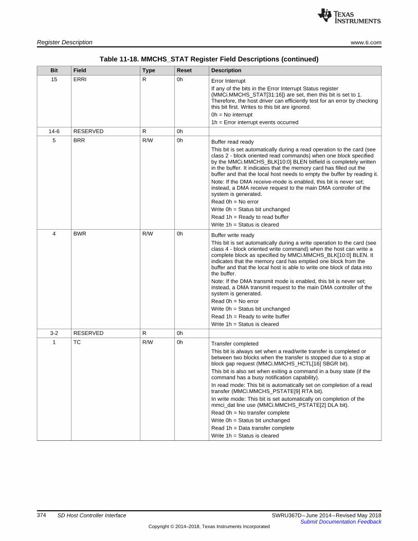
Register Description www.ti.com
374 SWRU367D–June 2014–Revised May 2018Submit Documentation Feedback
Copyright © 2014–2018, Texas Instruments Incorporated
SD Host Controller Interface
Table 11-18. MMCHS_STAT Register Field Descriptions (continued)Bit Field Type Reset Description15 ERRI R 0h Error Interrupt
If any of the bits in the Error Interrupt Status register(MMCi.MMCHS_STAT[31:16]) are set, then this bit is set to 1.Therefore, the host driver can efficiently test for an error by checkingthis bit first. Writes to this bit are ignored.0h = No interrupt1h = Error interrupt events occurred
14-6 RESERVED R 0h5 BRR R/W 0h Buffer read ready
This bit is set automatically during a read operation to the card (seeclass 2 - block oriented read commands) when one block specifiedby the MMCi.MMCHS_BLK[10:0] BLEN bitfield is completely writtenin the buffer. It indicates that the memory card has filled out thebuffer and that the local host needs to empty the buffer by reading it.Note: If the DMA receive-mode is enabled, this bit is never set;instead, a DMA receive request to the main DMA controller of thesystem is generated.Read 0h = No errorWrite 0h = Status bit unchangedRead 1h = Ready to read bufferWrite 1h = Status is cleared
4 BWR R/W 0h Buffer write readyThis bit is set automatically during a write operation to the card (seeclass 4 - block oriented write command) when the host can write acomplete block as specified by MMCi.MMCHS_BLK[10:0] BLEN. Itindicates that the memory card has emptied one block from thebuffer and that the local host is able to write one block of data intothe buffer.Note: If the DMA transmit mode is enabled, this bit is never set;instead, a DMA transmit request to the main DMA controller of thesystem is generated.Read 0h = No errorWrite 0h = Status bit unchangedRead 1h = Ready to write bufferWrite 1h = Status is cleared
3-2 RESERVED R 0h1 TC R/W 0h Transfer completed
This bit is always set when a read/write transfer is completed orbetween two blocks when the transfer is stopped due to a stop atblock gap request (MMCi.MMCHS_HCTL[16] SBGR bit).This bit is also set when exiting a command in a busy state (if thecommand has a busy notification capability).In read mode: This bit is automatically set on completion of a readtransfer (MMCi.MMCHS_PSTATE[9] RTA bit).In write mode: This bit is set automatically on completion of themmci_dat line use (MMCi.MMCHS_PSTATE[2] DLA bit).Read 0h = No transfer completeWrite 0h = Status bit unchangedRead 1h = Data transfer completeWrite 1h = Status is cleared
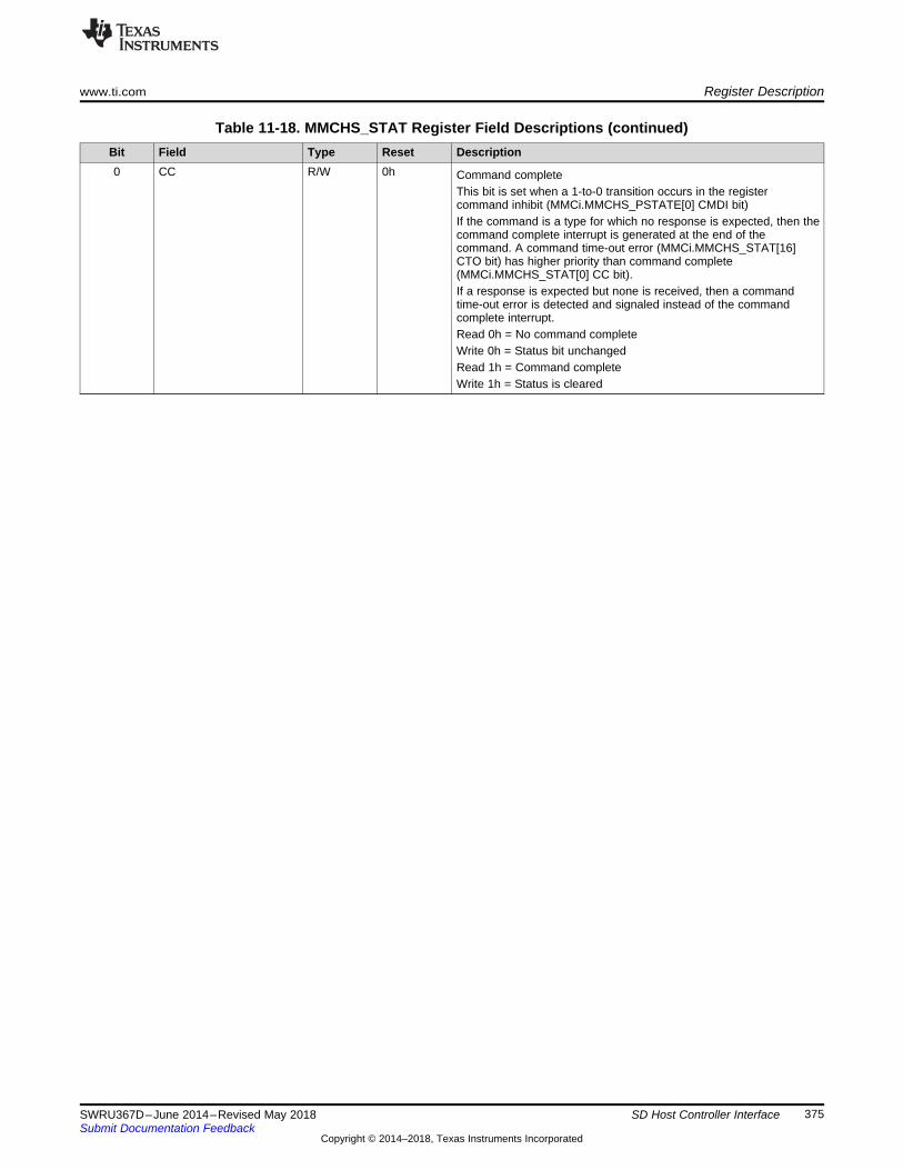
www.ti.com Register Description
375SWRU367D–June 2014–Revised May 2018Submit Documentation Feedback
Copyright © 2014–2018, Texas Instruments Incorporated
SD Host Controller Interface
Table 11-18. MMCHS_STAT Register Field Descriptions (continued)Bit Field Type Reset Description0 CC R/W 0h Command complete
This bit is set when a 1-to-0 transition occurs in the registercommand inhibit (MMCi.MMCHS_PSTATE[0] CMDI bit)If the command is a type for which no response is expected, then thecommand complete interrupt is generated at the end of thecommand. A command time-out error (MMCi.MMCHS_STAT[16]CTO bit) has higher priority than command complete(MMCi.MMCHS_STAT[0] CC bit).If a response is expected but none is received, then a commandtime-out error is detected and signaled instead of the commandcomplete interrupt.Read 0h = No command completeWrite 0h = Status bit unchangedRead 1h = Command completeWrite 1h = Status is cleared
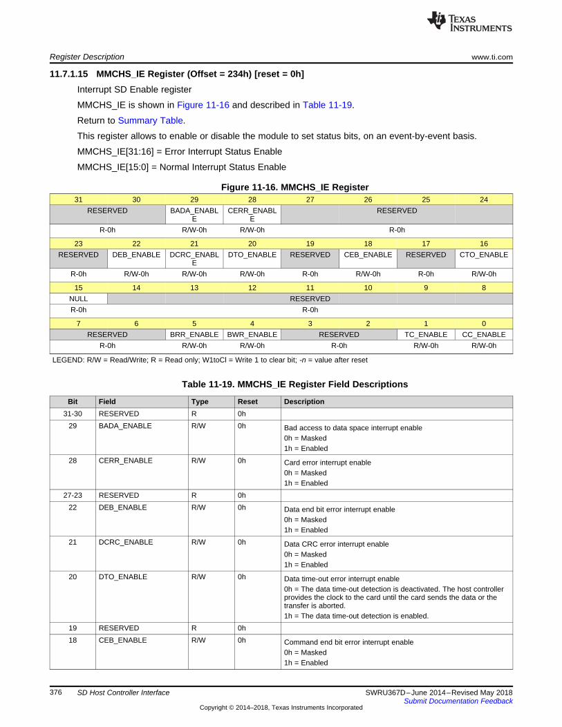
Register Description www.ti.com
376 SWRU367D–June 2014–Revised May 2018Submit Documentation Feedback
Copyright © 2014–2018, Texas Instruments Incorporated
SD Host Controller Interface
11.7.1.15 MMCHS_IE Register (Offset = 234h) [reset = 0h]Interrupt SD Enable register
MMCHS_IE is shown in Figure 11-16 and described in Table 11-19.
Return to Summary Table.
This register allows to enable or disable the module to set status bits, on an event-by-event basis.
MMCHS_IE[31:16] = Error Interrupt Status Enable
MMCHS_IE[15:0] = Normal Interrupt Status Enable
Figure 11-16. MMCHS_IE Register31 30 29 28 27 26 25 24
RESERVED BADA_ENABLE
CERR_ENABLE
RESERVED
R-0h R/W-0h R/W-0h R-0h
23 22 21 20 19 18 17 16RESERVED DEB_ENABLE DCRC_ENABL
EDTO_ENABLE RESERVED CEB_ENABLE RESERVED CTO_ENABLE
R-0h R/W-0h R/W-0h R/W-0h R-0h R/W-0h R-0h R/W-0h
15 14 13 12 11 10 9 8NULL RESERVEDR-0h R-0h
7 6 5 4 3 2 1 0RESERVED BRR_ENABLE BWR_ENABLE RESERVED TC_ENABLE CC_ENABLE
R-0h R/W-0h R/W-0h R-0h R/W-0h R/W-0h
LEGEND: R/W = Read/Write; R = Read only; W1toCl = Write 1 to clear bit; -n = value after reset
Table 11-19. MMCHS_IE Register Field Descriptions
Bit Field Type Reset Description31-30 RESERVED R 0h
29 BADA_ENABLE R/W 0h Bad access to data space interrupt enable0h = Masked1h = Enabled
28 CERR_ENABLE R/W 0h Card error interrupt enable0h = Masked1h = Enabled
27-23 RESERVED R 0h22 DEB_ENABLE R/W 0h Data end bit error interrupt enable
0h = Masked1h = Enabled
21 DCRC_ENABLE R/W 0h Data CRC error interrupt enable0h = Masked1h = Enabled
20 DTO_ENABLE R/W 0h Data time-out error interrupt enable0h = The data time-out detection is deactivated. The host controllerprovides the clock to the card until the card sends the data or thetransfer is aborted.1h = The data time-out detection is enabled.
19 RESERVED R 0h18 CEB_ENABLE R/W 0h Command end bit error interrupt enable
0h = Masked1h = Enabled

www.ti.com Register Description
377SWRU367D–June 2014–Revised May 2018Submit Documentation Feedback
Copyright © 2014–2018, Texas Instruments Incorporated
SD Host Controller Interface
Table 11-19. MMCHS_IE Register Field Descriptions (continued)Bit Field Type Reset Description17 RESERVED R 0h16 CTO_ENABLE R/W 0h Command time-out error interrupt enable
0h = Masked1h = Enabled
15 NULL R 0h Fixed to 0The host driver controls the error interrupts using the Error InterruptSignal Enable register.Writes to this bit are ignored.
14-6 RESERVED R 0h5 BRR_ENABLE R/W 0h Buffer read ready interrupt enable
0h = Masked1h = Enabled
4 BWR_ENABLE R/W 0h Buffer write ready interrupt enable0h = Masked1h = Enabled
3-2 RESERVED R 0h1 TC_ENABLE R/W 0h Transfer completed interrupt enable
0h = Masked1h = Enabled
0 CC_ENABLE R/W 0h Command completed interrupt enable0h = Masked1h = Enabled
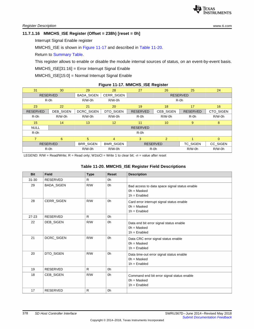
Register Description www.ti.com
378 SWRU367D–June 2014–Revised May 2018Submit Documentation Feedback
Copyright © 2014–2018, Texas Instruments Incorporated
SD Host Controller Interface
11.7.1.16 MMCHS_ISE Register (Offset = 238h) [reset = 0h]Interrupt Signal Enable register
MMCHS_ISE is shown in Figure 11-17 and described in Table 11-20.
Return to Summary Table.
This register allows to enable or disable the module internal sources of status, on an event-by-event basis.
MMCHS_ISE[31:16] = Error Interrupt Signal Enable
MMCHS_ISE[15:0] = Normal Interrupt Signal Enable
Figure 11-17. MMCHS_ISE Register31 30 29 28 27 26 25 24
RESERVED BADA_SIGEN CERR_SIGEN RESERVEDR-0h R/W-0h R/W-0h R-0h
23 22 21 20 19 18 17 16RESERVED DEB_SIGEN DCRC_SIGEN DTO_SIGEN RESERVED CEB_SIGEN RESERVED CTO_SIGEN
R-0h R/W-0h R/W-0h R/W-0h R-0h R/W-0h R-0h R/W-0h
15 14 13 12 11 10 9 8NULL RESERVEDR-0h R-0h
7 6 5 4 3 2 1 0RESERVED BRR_SIGEN BWR_SIGEN RESERVED TC_SIGEN CC_SIGEN
R-0h R/W-0h R/W-0h R-0h R/W-0h R/W-0h
LEGEND: R/W = Read/Write; R = Read only; W1toCl = Write 1 to clear bit; -n = value after reset
Table 11-20. MMCHS_ISE Register Field Descriptions
Bit Field Type Reset Description31-30 RESERVED R 0h
29 BADA_SIGEN R/W 0h Bad access to data space signal status enable0h = Masked1h = Enabled
28 CERR_SIGEN R/W 0h Card error interrupt signal status enable0h = Masked1h = Enabled
27-23 RESERVED R 0h22 DEB_SIGEN R/W 0h Data end bit error signal status enable
0h = Masked1h = Enabled
21 DCRC_SIGEN R/W 0h Data CRC error signal status enable0h = Masked1h = Enabled
20 DTO_SIGEN R/W 0h Data time-out error signal status enable0h = Masked1h = Enabled
19 RESERVED R 0h18 CEB_SIGEN R/W 0h Command end bit error signal status enable
0h = Masked1h = Enabled
17 RESERVED R 0h
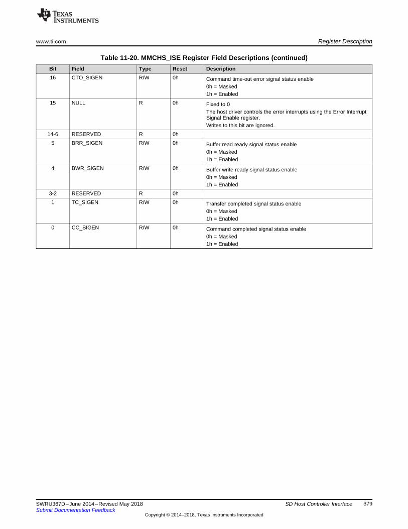
www.ti.com Register Description
379SWRU367D–June 2014–Revised May 2018Submit Documentation Feedback
Copyright © 2014–2018, Texas Instruments Incorporated
SD Host Controller Interface
Table 11-20. MMCHS_ISE Register Field Descriptions (continued)Bit Field Type Reset Description16 CTO_SIGEN R/W 0h Command time-out error signal status enable
0h = Masked1h = Enabled
15 NULL R 0h Fixed to 0The host driver controls the error interrupts using the Error InterruptSignal Enable register.Writes to this bit are ignored.
14-6 RESERVED R 0h5 BRR_SIGEN R/W 0h Buffer read ready signal status enable
0h = Masked1h = Enabled
4 BWR_SIGEN R/W 0h Buffer write ready signal status enable0h = Masked1h = Enabled
3-2 RESERVED R 0h1 TC_SIGEN R/W 0h Transfer completed signal status enable
0h = Masked1h = Enabled
0 CC_SIGEN R/W 0h Command completed signal status enable0h = Masked1h = Enabled
380 SWRU367D–June 2014–Revised May 2018Submit Documentation Feedback
Copyright © 2014–2018, Texas Instruments Incorporated
Inter-Integrated Sound (I2S) Multi-Channel Audio Serial Port
Chapter 12SWRU367D–June 2014–Revised May 2018
Inter-Integrated Sound (I2S) Multi-Channel Audio SerialPort
Topic ........................................................................................................................... Page
12.1 Overview ......................................................................................................... 38112.2 Functional Description ...................................................................................... 38212.3 Programming Model.......................................................................................... 38212.4 Peripheral Library APIs for I2S Configuration ...................................................... 385
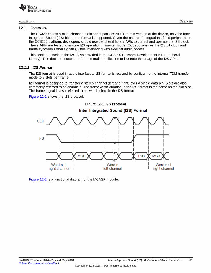
www.ti.com Overview
381SWRU367D–June 2014–Revised May 2018Submit Documentation Feedback
Copyright © 2014–2018, Texas Instruments Incorporated
Inter-Integrated Sound (I2S) Multi-Channel Audio Serial Port
12.1 OverviewThe CC3200 hosts a multi-channel audio serial port (MCASP). In this version of the device, only the Inter-Integrated Sound (I2S) bit stream format is supported. Given the nature of integration of this peripheral onthe CC3200 platform, developers should use peripheral library APIs to control and operate the I2S block.These APIs are tested to ensure I2S operation in master mode (CC3200 sources the I2S bit clock andframe synchronization signals), while interfacing with external audio codecs.
This section describes the I2S APIs provided in the CC3200 Software Development Kit [PeripheralLibrary]. This document uses a reference audio application to illustrate the usage of the I2S APIs.
12.1.1 I2S FormatThe I2S format is used in audio interfaces. I2S format is realized by configuring the internal TDM transfermode to 2 slots per frame.
I2S format is designed to transfer a stereo channel (left and right) over a single data pin. Slots are alsocommonly referred to as channels. The frame width duration in the I2S format is the same as the slot size.The frame signal is also referred to as 'word select' in the I2S format.
Figure 12-1 shows the I2S protocol.
Figure 12-1. I2S Protocol
Figure 12-2 is a functional diagram of the MCASP module.
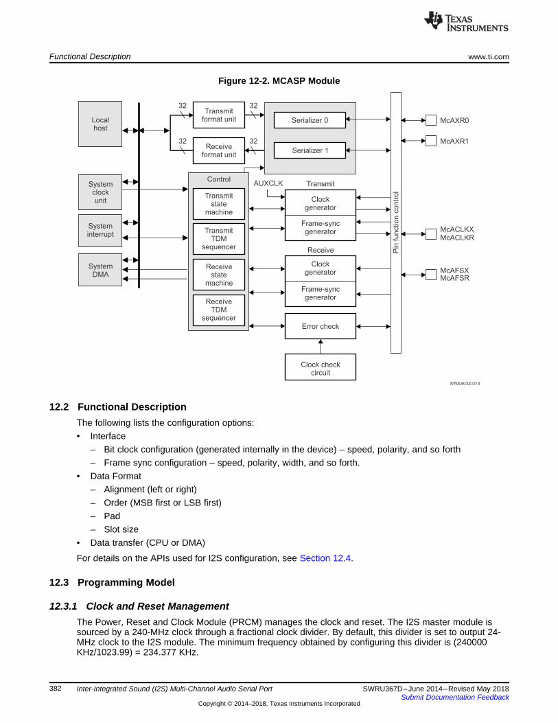
SWAS032-013
Localhost
Systemclockunit
Systeminterrupt
SystemDMA
32 32
32 32
Transmitformat unit
Receiveformat unit
Control
Transmitstate
machine
TransmitTDM
sequencer
Receivestate
machine
ReceiveTDM
sequencer
AUXCLK
Serializer 0
Serializer 1
Transmit
McAXR0
McACLKXMcACLKR
McAFSXMcAFSR
Pin
fu
nctio
n c
on
tro
l
Clockgenerator
Frame-syncgenerator
Receive
Error check
Clock checkcircuit
Clockgenerator
Frame-syncgenerator
McAXR1
Functional Description www.ti.com
382 SWRU367D–June 2014–Revised May 2018Submit Documentation Feedback
Copyright © 2014–2018, Texas Instruments Incorporated
Inter-Integrated Sound (I2S) Multi-Channel Audio Serial Port
Figure 12-2. MCASP Module
12.2 Functional DescriptionThe following lists the configuration options:• Interface
– Bit clock configuration (generated internally in the device) – speed, polarity, and so forth– Frame sync configuration – speed, polarity, width, and so forth.
• Data Format– Alignment (left or right)– Order (MSB first or LSB first)– Pad– Slot size
• Data transfer (CPU or DMA)
For details on the APIs used for I2S configuration, see Section 12.4.
12.3 Programming Model
12.3.1 Clock and Reset ManagementThe Power, Reset and Clock Module (PRCM) manages the clock and reset. The I2S master module issourced by a 240-MHz clock through a fractional clock divider. By default, this divider is set to output 24-MHz clock to the I2S module. The minimum frequency obtained by configuring this divider is (240000KHz/1023.99) = 234.377 KHz.
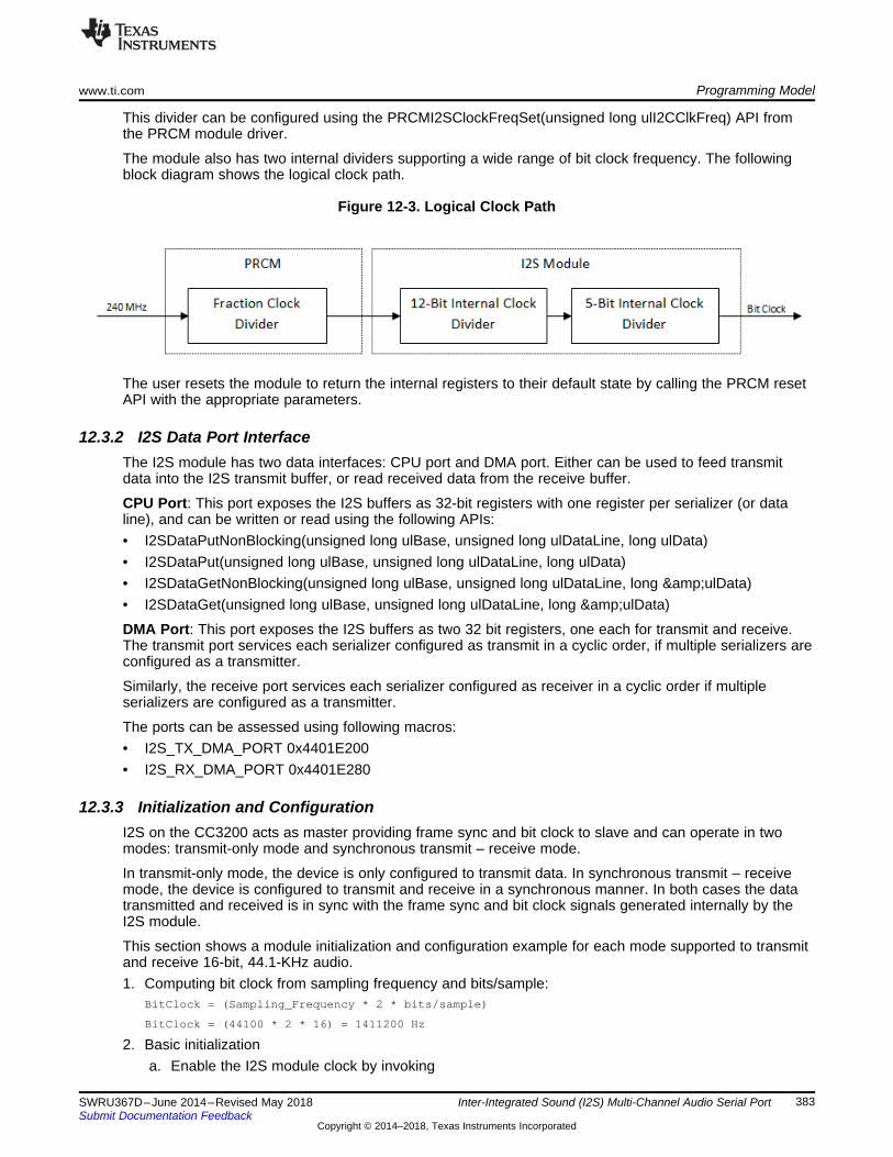
www.ti.com Programming Model
383SWRU367D–June 2014–Revised May 2018Submit Documentation Feedback
Copyright © 2014–2018, Texas Instruments Incorporated
Inter-Integrated Sound (I2S) Multi-Channel Audio Serial Port
This divider can be configured using the PRCMI2SClockFreqSet(unsigned long ulI2CClkFreq) API fromthe PRCM module driver.
The module also has two internal dividers supporting a wide range of bit clock frequency. The followingblock diagram shows the logical clock path.
Figure 12-3. Logical Clock Path
The user resets the module to return the internal registers to their default state by calling the PRCM resetAPI with the appropriate parameters.
12.3.2 I2S Data Port InterfaceThe I2S module has two data interfaces: CPU port and DMA port. Either can be used to feed transmitdata into the I2S transmit buffer, or read received data from the receive buffer.
CPU Port: This port exposes the I2S buffers as 32-bit registers with one register per serializer (or dataline), and can be written or read using the following APIs:• I2SDataPutNonBlocking(unsigned long ulBase, unsigned long ulDataLine, long ulData)• I2SDataPut(unsigned long ulBase, unsigned long ulDataLine, long ulData)• I2SDataGetNonBlocking(unsigned long ulBase, unsigned long ulDataLine, long &ulData)• I2SDataGet(unsigned long ulBase, unsigned long ulDataLine, long &ulData)
DMA Port: This port exposes the I2S buffers as two 32 bit registers, one each for transmit and receive.The transmit port services each serializer configured as transmit in a cyclic order, if multiple serializers areconfigured as a transmitter.
Similarly, the receive port services each serializer configured as receiver in a cyclic order if multipleserializers are configured as a transmitter.
The ports can be assessed using following macros:• I2S_TX_DMA_PORT 0x4401E200• I2S_RX_DMA_PORT 0x4401E280
12.3.3 Initialization and ConfigurationI2S on the CC3200 acts as master providing frame sync and bit clock to slave and can operate in twomodes: transmit-only mode and synchronous transmit – receive mode.
In transmit-only mode, the device is only configured to transmit data. In synchronous transmit – receivemode, the device is configured to transmit and receive in a synchronous manner. In both cases the datatransmitted and received is in sync with the frame sync and bit clock signals generated internally by theI2S module.
This section shows a module initialization and configuration example for each mode supported to transmitand receive 16-bit, 44.1-KHz audio.1. Computing bit clock from sampling frequency and bits/sample:
BitClock = (Sampling_Frequency * 2 * bits/sample)
BitClock = (44100 * 2 * 16) = 1411200 Hz
2. Basic initializationa. Enable the I2S module clock by invoking
Programming Model www.ti.com
384 SWRU367D–June 2014–Revised May 2018Submit Documentation Feedback
Copyright © 2014–2018, Texas Instruments Incorporated
Inter-Integrated Sound (I2S) Multi-Channel Audio Serial Port
PRCMPeripheralClkEnable(PRCM_I2S,PRCM_RUN_MODE_CLK).b. Reset the module using PRCMPeripheralReset(PRCM_I2S).c. Set fractional clock divider to generate module input clock of BitRate * 10:
PRCMI2SClockFreqSet(14112000)
d. Configure the internal divider of the module to generate the required bit clock frequency:I2SConfigSetExpClk(I2S_BASE, 14112000, 1411200, I2S_SLOT_SIZE_16|I2S_PORT_CPU).
The second parameter “I2S_SLOT_SIZE_16|I2S_PORT_CPU” sets the slot size and chooses theport interface on which the I2C module should expect the data.
e. Register the interrupt handler and enable the transmit data interrupt:I2SIntRegister(I2S_BASE, I2SIntHandler)
I2SIntEnable(I2S_BASE,I2S_INT_XDATA)
3. Transmit-only mode with interruptsa. Configure the serializer 0 for transmit:
I2SSerializerConfig(I2S_BASE, I2S_DATA_LINE_0,I2S_SER_MODE_TX, I2S_INACT_LOW_LEVEL)
b. Enable I2S module in transmit-only mode:I2SEnable(I2S_BASE, I2S_MODE_TX_ONLY)
4. Synchronous transmit – receive with interruptsa. Enable receive data Interrupt:
I2SIntEnable(I2S_BASE,I2S_INT_XDATA)
b. Configure the serializer 0 for transmit and serializer 1 for receive:I2SSerializerConfig(I2S_BASE, I2S_DATA_LINE_0, I2S_SER_MODE_TX, I2S_INACT_LOW_LEVEL)
I2SSerializerConfig(I2S_BASE, I2S_DATA_LINE_1, I2S_SER_MODE_RX, I2S_INACT_LOW_LEVEL)
c. Enable I2S module in synchronous transmit – receive mode:I2SEnable(I2S_BASE, I2S_MODE_TX_RX_SYNC)
5. Generic I2S interrupt handlervoid I2SIntHandler()unsigned long ulStatus;unsigned long ulDummy;
// Get the interrupt statusulStatus = I2SIntStatus(I2S_BASE);
// Check if there was a Transmit interrupt; if so write next data into the tx buffer andacknowledge// the interruptif(ulStatus&I2S_STS_XDATA)
I2SDataPutNonBlocking(I2S_BASE,I2S_DATA_LINE_0,0xA5)I2SIntClear(I2S_BASE,I2S_STS_XDATA);
// Check if there was a receive interrupt; if so read the data from the rx buffer andacknowledge// the interruptif(ulStatus&I2S_STS_RDATA)
I2SDataGetNonBlocking( I2S_BASE, I2S_DATA_LINE_1,&ulDummy);
I2SIntClear(I2S_BASE,I2S_STS_RDATA);
www.ti.com Peripheral Library APIs for I2S Configuration
385SWRU367D–June 2014–Revised May 2018Submit Documentation Feedback
Copyright © 2014–2018, Texas Instruments Incorporated
Inter-Integrated Sound (I2S) Multi-Channel Audio Serial Port
12.4 Peripheral Library APIs for I2S ConfigurationThis section describes the APIs hosted in the CC3200 SDK (Peripheral Library) necessary for I2Sconfiguration.
12.4.1 Basic APIs for Enabling and Configuring the Interface
void I2SDisable (unsigned long ulBase)Disables transmit and/or receive.
Parameters:ulBase — the base address of the I2S module.
This function disables transmit, receive, or both from the I2S module.
Returns:None.
12.4.1.1 void I2SEnable (unsigned long ulBase, unsigned long ulMode)Enables transmit and/or receive.
Parameters:ulBase — is the base address of the I2S module.
ulMode — is one of the valid modes.
This function enables the I2S module in specified mode.
The parameter ulMode should be one of the following:-I2S_MODE_TX_ONLY -I2S_MODE_TX_RX_SYNC
Returns:None.
Reference:ulModeparameter
#define I2S_MODE_TX_ONLY 0x00000001 #defineI2S_MODE_TX_RX_SYNC 0x00000003
12.4.1.2 void I2SSerializerConfig (unsigned long ulBase, unsigned long ulDataLine, unsigned longulSerMode, unsigned long ulInActState)
Configure the serializer in a specified mode.
Parameters:ulBase — is the base address of the I2S module.
ulDataLine — is the data line (serilizer) to be configured.
ulSerMode — is the required serializer mode.
ulInActState — sets the inactive state of the data line.
This function configures and enables the serializer associated with the given data line in specified mode.
Peripheral Library APIs for I2S Configuration www.ti.com
386 SWRU367D–June 2014–Revised May 2018Submit Documentation Feedback
Copyright © 2014–2018, Texas Instruments Incorporated
Inter-Integrated Sound (I2S) Multi-Channel Audio Serial Port
The parameter ulDataLine selects the data line to be configured, and can be one of the following:-I2S_DATA_LINE_0 -I2S_DATA_LINE_1
The parameter ulSerMode can be one of the following:-I2S_SER_MODE_TX -I2S_SER_MODE_RX
-I2S_SER_MODE_DISABLE
The parameter ulInActState can be one of the following:-I2S_INACT_TRI_STATE -I2S_INACT_LOW_LEVEL
-I2S_INACT_LOW_HIGH
Returns:Returns receive FIFO status.
References:ulDataLine parameter
#define I2S_DATA_LINE_0 0x00000001 #defineI2S_DATA_LINE_1 0x00000002
ulSerMode parameter#define I2S_SER_MODE_TX 0x00000001 #define
I2S_SER_MODE_RX 0x00000002 #define I2S_SER_MODE_DISABLE0x00000000
ulInActState parameter#define I2S_INACT_TRI_STATE 0x00000000 #define
I2S_INACT_LOW_LEVEL 0x00000008 #define I2S_INACT_HIGH_LEVEL0x0000000C
12.4.1.3 void I2SConfigSetExpClk (unsigned long ulBase, unsigned long ulI2SClk, unsigned longulBitClk, unsigned long ulConfig)
Sets the configuration of the I2S module.
Parameters:ulBase — is the base address of the I2S module.
ulI2SClk — is the rate of the clock supplied to the I2S module.
ulBitClk — is the desired bit rate.
ulConfig — is the data format.
This function configures the I2S for operation in the specified data format. The bit rate is provided in theulBitClk parameter and the data format in the ulConfig parameter.
The ulConfig parameter is the logical OR of two values: the slot size and the data read/write port select.
The following parameters select the slot size:-I2S_SLOT_SIZE_24 -I2S_SLOT_SIZE_16
The following parameters select the data read/write port:-I2S_PORT_DMA -I2S_PORT_CPU
Returns:
www.ti.com Peripheral Library APIs for I2S Configuration
387SWRU367D–June 2014–Revised May 2018Submit Documentation Feedback
Copyright © 2014–2018, Texas Instruments Incorporated
Inter-Integrated Sound (I2S) Multi-Channel Audio Serial Port
None.
Reference:#define I2S_SLOT_SIZE_24 0x00B200B4 #define
I2S_SLOT_SIZE_16 0x00700074 #define I2S_PORT_CPU 0x00000008 #defineI2S_PORT_DMA 0x00000000
Peripheral Library APIs for I2S Configuration www.ti.com
388 SWRU367D–June 2014–Revised May 2018Submit Documentation Feedback
Copyright © 2014–2018, Texas Instruments Incorporated
Inter-Integrated Sound (I2S) Multi-Channel Audio Serial Port
12.4.2 APIs for Data Access if DMA is Not Used
12.4.2.1 void I2SDataGet (unsigned long ulBase, unsigned long ulDataLine, unsigned long * pulData)Waits for data from the specified data line.
Parameters:ulBase — is the base address of the I2S module.
ulDataLine — is one of the valid data lines.
pulData — is a pointer to the receive data variable.
This function gets data from the receive register for the specified data line. If there is no data available,this function waits until a receive before returning.
Returns:None.
12.4.2.2 long I2SDataGetNonBlocking (unsigned long ulBase, unsigned long ulDataLine, unsigned long* pulData)
Receives data from the specified data line.
Parameters:ulBase — is the base address of the I2S module.
ulDataLine — is one of the valid data lines.
pulData — is a pointer to the receive data variable.
This function gets data from the receive register for the specified data line.
Returns:Returns 0 on success, -1 otherwise.
12.4.2.3 void I2SDataPut (unsigned long ulBase, unsigned long ulDataLine, unsigned long ulData)Waits to send data over the specified data line.
Parameters:ulBase — is the base address of the I2S module.
ulDataLine — is one of the valid data lines.
ulData — is the data to be transmitted.
This function sends the ucData to the transmit register for the specified data line. If there is no spaceavailable, this function waits until there is space available before returning.
Returns:None.
12.4.2.4 void I2SDataPut (unsigned long ulBase, unsigned long ulDataLine, unsigned long ulData)Waits to send data over the specified data line.
www.ti.com Peripheral Library APIs for I2S Configuration
389SWRU367D–June 2014–Revised May 2018Submit Documentation Feedback
Copyright © 2014–2018, Texas Instruments Incorporated
Inter-Integrated Sound (I2S) Multi-Channel Audio Serial Port
Parameters:ulBase — is the base address of the I2S module.
ulDataLine — is one of the valid data lines.
ulData — is the data to be transmitted.
This function writes the ucData to the transmit register for the specified data line. This function does notblock, so if there is no space available, then –1 is returned, and the application must retry the functionlater.
Returns:Returns 0 on success, -1 otherwise.
Peripheral Library APIs for I2S Configuration www.ti.com
390 SWRU367D–June 2014–Revised May 2018Submit Documentation Feedback
Copyright © 2014–2018, Texas Instruments Incorporated
Inter-Integrated Sound (I2S) Multi-Channel Audio Serial Port
12.4.3 APIs for Setting Up, Handling Interrupts, or Getting Status from I2S Peripheral
12.4.3.1 void I2SIntRegister (unsigned long ulBase, void(*)(void) pfnHandler)Registers an interrupt handler for an I2S interrupt.
Parameters:ulBase — is the base address of the I2S module.
pfnHandler — is a pointer to the function to be called when the I2S interrupt occurs.
This function registers the interrupt handler. This function enables the global interrupt in the interruptcontroller; specific I2S interrupts must be enabled using I2SIntEnable(). The interrupt handler mustclear the interrupt source.See IntRegister() for information about registering interrupt handlers.
Returns:None.
12.4.3.2 void I2SIntEnable (unsigned long ulBase, unsigned long ulIntFlags)Enables individual I2S interrupt sources.
Parameters:ulBase — is the base address of the I2S module.
ulIntFlags — is the bit mask of the interrupt sources to be enabled.
This function enables the indicated I2S interrupt sources. Only enabled sources can be reflected to theprocessor interrupt; disabled sources have no effect on the processor.The ulIntFlags parameter is the logical OR for any of the following:-I2S_INT_XUNDRN -I2S_INT_XSYNCERR -I2S_INT_XLAST -I2S_INT_XDATA
-I2S_INT_XSTAFRM -I2S_INT_XDMA -I2S_INT_ROVRN -I2S_INT_RSYNCERR-I2S_INT_RLAST -I2S_INT_RDATA -I2S_INT_RSTAFRM -I2S_INT_RDMA
Returns:None.
12.4.3.3 void I2SIntDisable (unsigned long ulBase, unsigned long ulIntFlags)Disables individual I2S interrupt sources.
Parameters:ulBase — is the base address of the I2S module.
ulIntFlags — is the bit mask of the interrupt sources to be disabled.
This function disables the indicated I2S interrupt sources. Only enabled sources can be reflected to theprocessor interrupt; disabled sources have no effect on the processor.The ulIntFlags parameter has the same definition as the ulIntFlags parameter to
I2SIntEnable().
Returns:None.
www.ti.com Peripheral Library APIs for I2S Configuration
391SWRU367D–June 2014–Revised May 2018Submit Documentation Feedback
Copyright © 2014–2018, Texas Instruments Incorporated
Inter-Integrated Sound (I2S) Multi-Channel Audio Serial Port
12.4.3.4 unsigned long I2SIntStatus (unsigned long ulBase)Gets the current interrupt status.
Parameters:ulBase — is the base address of the I2S module.
This function returns the raw interrupt status for I2S enumerated as a bit field of values:-I2S_STS_XERR -I2S_STS_XDMAERR -I2S_STS_XSTAFRM -I2S_STS_XDATA
-I2S_STS_XLAST -I2S_STS_XSYNCERR -I2S_STS_XUNDRN -I2S_STS_XDMA-I2S_STS_RERR -I2S_STS_RDMAERR -I2S_STS_RSTAFRM -I2S_STS_RDATA-I2S_STS_RLAST -I2S_STS_RSYNCERR -I2S_STS_ROVERN -I2S_STS_RDMA
Returns:Returns the current interrupt status, enumerated as a bit field of the values described above.
12.4.3.5 void I2SIntUnregister (unsigned long ulBase)Unregisters an interrupt handler for a I2S interrupt.
Parameters:ulBase — is the base address of the I2S module.
This function unregisters the interrupt handler. The function clears the handler to be called when a I2Sinterrupt occurs. This function also masks off the interrupt in the interrupt controller so that the interrupthandler no longer is called.See IntRegister() for information about registering interrupt handlers.
Returns:None.
12.4.3.6 void I2SIntClear (unsigned long ulBase, unsigned long ulStatFlags)Clears I2S interrupt sources.
Parameters:ulBase — is the base address of the I2S module.
ulStatFlags — is a bit mask of the interrupt sources to be cleared.
The specified I2S interrupt sources are cleared, so that they no longer assert. This function must be calledin the interrupt handler to keep the interrupt from being recognized again immediately upon exit.The ulIntFlags parameter is the logical OR of any of the value described in
I2SIntStatus().
Returns:None.
12.4.3.7 Values that can be passed to I2SIntEnable() and I2SIntDisable() as the ulIntFlags parameterTable 12-1 lists the values that can be passed to I2SIntEnable() and I2SIntDisable() as theulIntFlags parameter.

Peripheral Library APIs for I2S Configuration www.ti.com
392 SWRU367D–June 2014–Revised May 2018Submit Documentation Feedback
Copyright © 2014–2018, Texas Instruments Incorporated
Inter-Integrated Sound (I2S) Multi-Channel Audio Serial Port
Table 12-1. ulIntFlags Parameter
Tag Value DescriptionI2S_INT_XUNDR 0x00000001 Transmit underrun interrupt enable bitI2S_INT_XSYNCERR 0x00000002 Unexpected transmit frame sync interrupt enable bitI2S_INT_XLAST 0x00000010 Transmit last slot interrupt enable bitI2S_INT_XDATA 0x00000020 Transmit data ready interrupt enable bitI2S_INT_XSTAFRM 0x00000080 Transmit start of frame interrupt enable bitI2S_INT_XDMA 0x80000000I2S_INT_ROVRN 0x00010000 Receiver overrun interrupt enable bitI2S_INT_RSYNCERR 0x00020000 Unexpected receive frame sync interrupt enable bitI2S_INT_RLAST 0x00100000 Receive start of frame interrupt enable bitI2S_INT_RDATA 0x00200000 Receive data ready interrupt enable bitI2S_INT_RSTAFRM 0x00800000 Receive start of frame interrupt enable bitI2S_INT_RDMA 0x40000000
12.4.3.8 Values that can be passed to I2SIntClear() as the ulStatFlags parameter and returned fromI2SIntStatus()
Table 12-2 lists the values that can be passed to I2SIntClear() as the ulStatFlags parameter andreturned from I2SIntStatus().
Table 12-2. ulStatFlags Parameter
Tag Value DescriptionI2S_STS_XERR 0x00000100 XERR bit always returns a logic-OR of: XUNDRN |
XSYNCERR | XCKFAIL | XDMAERRI2S_STS_XDMAERR 0x00000080 Transmit DMA error flag. XDMAERR is set when the
CPU or DMA writes more serializers through the dataport in a given time slot than were programmed astransmitters
I2S_STS_XSTAFRM 0x00000040 Transmit start of frame flagI2S_STS_XDATA 0x00000020 Transmit data ready flag. 1 indicates that data is copied
from Tx Buffer to shift register. Tx Buffer is EMPTY andready to be written. 0 indicates Tx Buffer is FULL
I2S_STS_XLAST 0x00000010 Transmit last slot flag. XLAST is set along with XDATA, ifthe current slot is the last slot in a frame.
I2S_STS_XSYNCERR 0x00000002 Unexpected transmit frame sync flag. XSYNCERR is setwhen a new transmit frame sync (AFSX) occurs before itis expected.
I2S_STS_XUNDRN 0x00000001 Transmitter underrun flag. XUNDRN is set when thetransmit serializer is instructed to transfer data from TxBuffer, but Tx Buffer has not yet been serviced with newdata since the last transfer.
I2S_STS_XDMA 0x80000000I2S_STS_RERR 0x01000000 RERR bit always returns a logic-OR of: ROVRN |
RSYNCERR | RCKFAIL | RDMAERR. Allows a single bitto be checked to determine if a receiver error interrupthas occurred.
I2S_STS_RDMAERR 0x00800000 Receive DMA error. Receive DMA error flag. RDMAERRis set when the CPU or DMA reads more serializersthrough the data port in a given time slot than wereprogrammed as receivers
I2S_STS_RSTAFRM 0x00400000 Receive start of frame flag. Indicates A new receiveframe sync is detected
I2S_STS_RDATA 0x00200000 Receive data ready flag. Indicates data is transferredfrom shift register to Rx buffer and ready to be servicedby the CPU or DMA. When RDATA is set, it alwayscauses a DMA event.
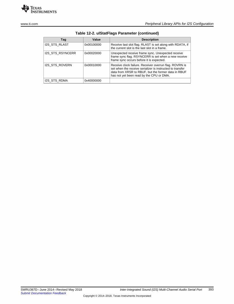
www.ti.com Peripheral Library APIs for I2S Configuration
393SWRU367D–June 2014–Revised May 2018Submit Documentation Feedback
Copyright © 2014–2018, Texas Instruments Incorporated
Inter-Integrated Sound (I2S) Multi-Channel Audio Serial Port
Table 12-2. ulStatFlags Parameter (continued)Tag Value Description
I2S_STS_RLAST 0x00100000 Receive last slot flag. RLAST is set along with RDATA, ifthe current slot is the last slot in a frame.
I2S_STS_RSYNCERR 0x00020000 Unexpected receive frame sync. Unexpected receiveframe sync flag. RSYNCERR is set when a new receiveframe sync occurs before it is expected.
I2S_STS_ROVERN 0x00010000 Receive clock failure. Receiver overrun flag. ROVRN isset when the receive serializer is instructed to transferdata from XRSR to RBUF, but the former data in RBUFhas not yet been read by the CPU or DMA.
I2S_STS_RDMA 0x40000000
Peripheral Library APIs for I2S Configuration www.ti.com
394 SWRU367D–June 2014–Revised May 2018Submit Documentation Feedback
Copyright © 2014–2018, Texas Instruments Incorporated
Inter-Integrated Sound (I2S) Multi-Channel Audio Serial Port
12.4.4 APIs to Control FIFO Structures Associated with I2S Peripheral
12.4.4.1 void I2SRxFIFODisable (unsigned long ulBase)Disables receive FIFO.
Parameters:ulBase — is the base address of the I2S module.
This function disables the I2S receive FIFO.
Returns:None.
12.4.4.2 void I2SRxFIFOEnable (unsigned long ulBase, unsigned long ulRxLevel, unsigned longulWordsPerTransfer)
Configures and enables receive FIFO.
Parameters:ulBase — is the base address of the I2S module.
ulRxLevel — is the receive FIFO DMA request level.
ulWordsPerTransfer — is the nuber of words transferred from theFIFO.
This function configures and enables I2S receive FIFO.The parameter ulRxLevel sets the level at which receive DMA requests are generated. This should benon-zero integer multiple of number of serializers enabled as receivers.The parameter ulWordsPerTransfer sets the number of words transferred to the receive FIFO from thedata lines. This value must equal the number of serializers used as receivers.
Returns:None.
12.4.4.3 unsigned long I2SRxFIFOStatusGet (unsigned long ulBase)Get the receive FIFO status.
Parameters:ulBase — is the base address of the I2S module.
This function gets the number of 32-bit words currently in the receive FIFO.
Returns:Returns receive FIFO status.
12.4.4.4 void I2STxFIFODisable (unsigned long ulBase)Disables transmit FIFO.
Parameters:ulBase — is the base address of the I2S module.
www.ti.com Peripheral Library APIs for I2S Configuration
395SWRU367D–June 2014–Revised May 2018Submit Documentation Feedback
Copyright © 2014–2018, Texas Instruments Incorporated
Inter-Integrated Sound (I2S) Multi-Channel Audio Serial Port
This function disables the I2S transmit FIFO.
Returns:None.
12.4.4.5 void I2STxFIFOEnable (unsigned long ulBase, unsigned long ulTxLevel, unsigned longulWordsPerTransfer)
Configures and enables transmit FIFO.
Parameters:ulBase — is the base address of the I2S module.
ulTxLevel — is the transmit FIFO DMA request level.
ulWordsPerTransfer — is the number of words transferred from theFIFO.
This function configures and enables I2S transmit FIFO.The parameter ulTxLevel sets the level at which transmit DMA requests are generated. This should benon-zero integer multiple of number of serializers enabled as transmitters.The parameter ulWordsPerTransfer sets the number of words that are transferred from the transmitFIFO to the data lines. This value must equal the number of serializers used as transmitters.
Returns:None.
12.4.4.6 unsigned long I2STxFIFOStatusGet (unsigned long ulBase)Gets the transmit FIFO status.
Parameters:ulBase — is the base address of the I2S module.
This function gets the number of 32-bit words currently in the transmit FIFO.
Returns:Returns transmit FIFO status.
396 SWRU367D–June 2014–Revised May 2018Submit Documentation Feedback
Copyright © 2014–2018, Texas Instruments Incorporated
Analog-to-Digital Converter [ADC]
Chapter 13SWRU367D–June 2014–Revised May 2018
Analog-to-Digital Converter [ADC]
Topic ........................................................................................................................... Page
13.1 Overview ......................................................................................................... 39713.2 Key Features.................................................................................................... 39713.3 ADC Register Mapping ...................................................................................... 39813.4 ADC_MODULE Registers ................................................................................... 39913.5 Initialization and Configuration .......................................................................... 42013.6 Peripheral Library APIs for ADC Operation .......................................................... 421
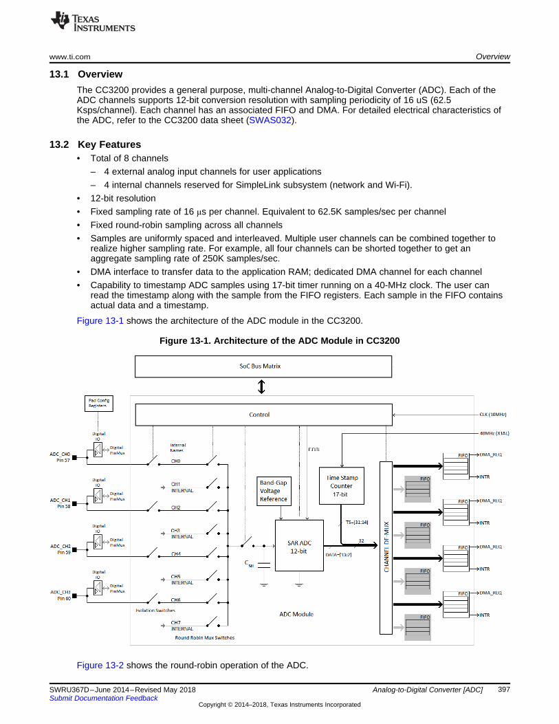
www.ti.com Overview
397SWRU367D–June 2014–Revised May 2018Submit Documentation Feedback
Copyright © 2014–2018, Texas Instruments Incorporated
Analog-to-Digital Converter [ADC]
13.1 OverviewThe CC3200 provides a general purpose, multi-channel Analog-to-Digital Converter (ADC). Each of theADC channels supports 12-bit conversion resolution with sampling periodicity of 16 uS (62.5Ksps/channel). Each channel has an associated FIFO and DMA. For detailed electrical characteristics ofthe ADC, refer to the CC3200 data sheet (SWAS032).
13.2 Key Features• Total of 8 channels
– 4 external analog input channels for user applications– 4 internal channels reserved for SimpleLink subsystem (network and Wi-Fi).
• 12-bit resolution• Fixed sampling rate of 16 μs per channel. Equivalent to 62.5K samples/sec per channel• Fixed round-robin sampling across all channels• Samples are uniformly spaced and interleaved. Multiple user channels can be combined together to
realize higher sampling rate. For example, all four channels can be shorted together to get anaggregate sampling rate of 250K samples/sec.
• DMA interface to transfer data to the application RAM; dedicated DMA channel for each channel• Capability to timestamp ADC samples using 17-bit timer running on a 40-MHz clock. The user can
read the timestamp along with the sample from the FIFO registers. Each sample in the FIFO containsactual data and a timestamp.
Figure 13-1 shows the architecture of the ADC module in the CC3200.
Figure 13-1. Architecture of the ADC Module in CC3200
Figure 13-2 shows the round-robin operation of the ADC.
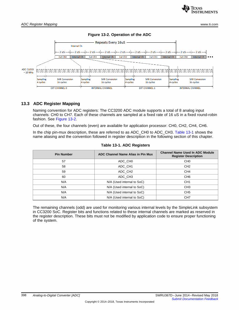
ADC Register Mapping www.ti.com
398 SWRU367D–June 2014–Revised May 2018Submit Documentation Feedback
Copyright © 2014–2018, Texas Instruments Incorporated
Analog-to-Digital Converter [ADC]
Figure 13-2. Operation of the ADC
13.3 ADC Register MappingNaming convention for ADC registers: The CC3200 ADC module supports a total of 8 analog inputchannels: CH0 to CH7. Each of these channels are sampled at a fixed rate of 16 uS in a fixed round-robinfashion. See Figure 13-2.
Out of these, the four channels (even) are available for application processor: CH0, CH2, CH4, CH6.
In the chip pin-mux description, these are referred to as ADC_CH0 to ADC_CH3. Table 13-1 shows thename aliasing and the convention followed in register description in the following section of this chapter.
Table 13-1. ADC Registers
Pin Number ADC Channel Name Alias in Pin Mux Channel Name Used In ADC ModuleRegister Description
57 ADC_CH0 CH058 ADC_CH1 CH259 ADC_CH2 CH460 ADC_CH3 CH6N/A N/A (Used internal to SoC) CH1N/A N/A (Used internal to SoC) CH3N/A N/A (Used internal to SoC) CH5N/A N/A (Used internal to SoC) CH7
The remaining channels (odd) are used for monitoring various internal levels by the SimpleLink subsystemin CC3200 SoC. Register bits and functions related to these internal channels are marked as reserved inthe register description. These bits must not be modified by application code to ensure proper functioningof the system.
www.ti.com ADC_MODULE Registers
399SWRU367D–June 2014–Revised May 2018Submit Documentation Feedback
Copyright © 2014–2018, Texas Instruments Incorporated
Analog-to-Digital Converter [ADC]
13.4 ADC_MODULE RegistersTable 13-2 lists the memory-mapped registers for the ADC_MODULE. All register offset addresses notlisted in Table 13-2 should be considered as reserved locations and the register contents should not bemodified.
Table 13-2. ADC_MODULE Registers
Offset Acronym Register Name Section0h ADC_CTRL ADC control register Section 13.4.1.124h ADC_CH0_IRQ_EN Channel 0 interrupt enable register Section 13.4.1.22Ch ADC_CH2_IRQ_EN Channel 2 interrupt enable register Section 13.4.1.334h ADC_CH4_IRQ_EN Channel 4 interrupt enable register Section 13.4.1.43Ch ADC_CH6_IRQ_EN Channel 6 interrupt enable register Section 13.4.1.544h ADC_CH0_IRQ_STATUS Channel 0 interrupt status register Section 13.4.1.64Ch ADC_CH2_IRQ_STATUS Channel 2 interrupt status register Section 13.4.1.754h ADC_CH4_IRQ_STATUS Channel 4 interrupt status register Section 13.4.1.85Ch ADC_CH6_IRQ_STATUS Channel 6 interrupt status register Section 13.4.1.964h ADC_DMA_MODE_EN DMA mode enable register Section 13.4.1.1068h ADC_TIMER_CONFIGURATION ADC timer configuration register Section 13.4.1.1170h ADC_TIMER_CURRENT_COUNT ADC timer current count register Section 13.4.1.1274h CHANNEL0FIFODATA CH0 FIFO DATA register Section 13.4.1.137Ch CHANNEL2FIFODATA CH2 FIFO DATA register Section 13.4.1.1484h CHANNEL4FIFODATA CH4 FIFO DATA register Section 13.4.1.158Ch CHANNEL6FIFODATA CH6 FIFO DATA register Section 13.4.1.1694h ADC_CH0_FIFO_LVL Channel 0 interrupt status register Section 13.4.1.179Ch ADC_CH2_FIFO_LVL Channel 2 interrupt status register Section 13.4.1.18A4h ADC_CH4_FIFO_LVL Channel 4 interrupt status register Section 13.4.1.19ACh ADC_CH6_FIFO_LVL Channel 6 interrupt status register Section 13.4.1.20B8h ADC_CH_ENABLE ADC enable register for application channels Section 13.4.1.21
13.4.1 ADC Register DescriptionThe remainder of this section lists and describes the ADC registers, in numerical order by address offset.
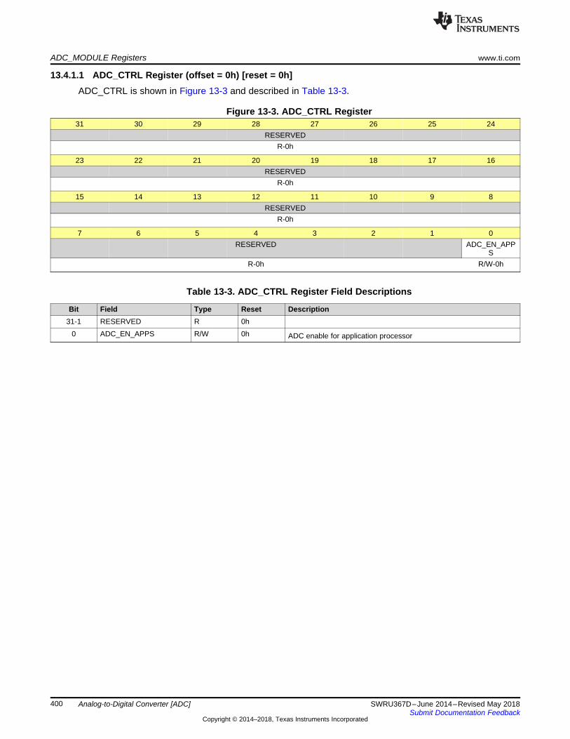
ADC_MODULE Registers www.ti.com
400 SWRU367D–June 2014–Revised May 2018Submit Documentation Feedback
Copyright © 2014–2018, Texas Instruments Incorporated
Analog-to-Digital Converter [ADC]
13.4.1.1 ADC_CTRL Register (offset = 0h) [reset = 0h]ADC_CTRL is shown in Figure 13-3 and described in Table 13-3.
Figure 13-3. ADC_CTRL Register31 30 29 28 27 26 25 24
RESERVEDR-0h
23 22 21 20 19 18 17 16RESERVED
R-0h
15 14 13 12 11 10 9 8RESERVED
R-0h
7 6 5 4 3 2 1 0RESERVED ADC_EN_APP
SR-0h R/W-0h
Table 13-3. ADC_CTRL Register Field Descriptions
Bit Field Type Reset Description31-1 RESERVED R 0h
0 ADC_EN_APPS R/W 0h ADC enable for application processor
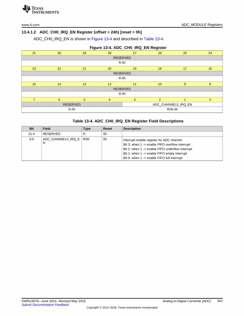
www.ti.com ADC_MODULE Registers
401SWRU367D–June 2014–Revised May 2018Submit Documentation Feedback
Copyright © 2014–2018, Texas Instruments Incorporated
Analog-to-Digital Converter [ADC]
13.4.1.2 ADC_CH0_IRQ_EN Register (offset = 24h) [reset = 0h]ADC_CH0_IRQ_EN is shown in Figure 13-4 and described in Table 13-4.
Figure 13-4. ADC_CH0_IRQ_EN Register31 30 29 28 27 26 25 24
RESERVEDR-0h
23 22 21 20 19 18 17 16RESERVED
R-0h
15 14 13 12 11 10 9 8RESERVED
R-0h
7 6 5 4 3 2 1 0RESERVED ADC_CHANNEL0_IRQ_EN
R-0h R/W-0h
Table 13-4. ADC_CH0_IRQ_EN Register Field Descriptions
Bit Field Type Reset Description31-4 RESERVED R 0h3-0 ADC_CHANNEL0_IRQ_E
NR/W 0h Interrupt enable register for ADC channel
Bit 3: when 1 -> enable FIFO overflow interruptBit 2: when 1 -> enable FIFO underflow interruptBit 1: when 1 -> enable FIFO empty interruptBit 0: when 1 -> enable FIFO full interrupt
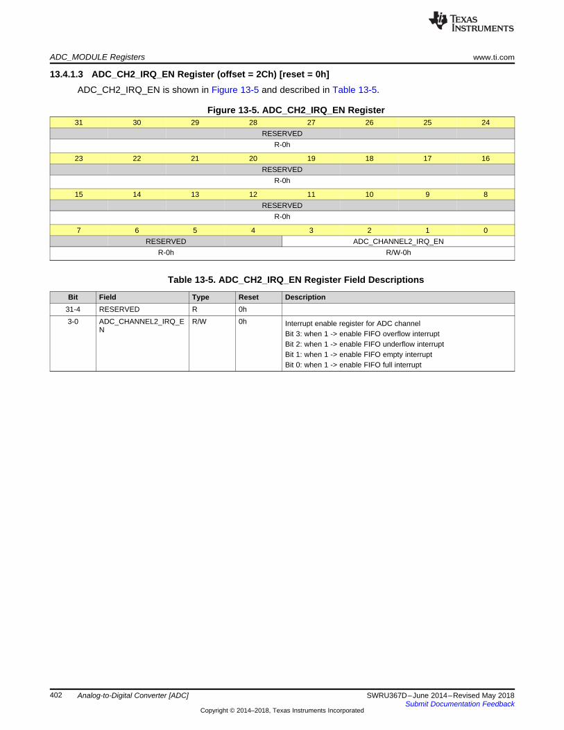
ADC_MODULE Registers www.ti.com
402 SWRU367D–June 2014–Revised May 2018Submit Documentation Feedback
Copyright © 2014–2018, Texas Instruments Incorporated
Analog-to-Digital Converter [ADC]
13.4.1.3 ADC_CH2_IRQ_EN Register (offset = 2Ch) [reset = 0h]ADC_CH2_IRQ_EN is shown in Figure 13-5 and described in Table 13-5.
Figure 13-5. ADC_CH2_IRQ_EN Register31 30 29 28 27 26 25 24
RESERVEDR-0h
23 22 21 20 19 18 17 16RESERVED
R-0h
15 14 13 12 11 10 9 8RESERVED
R-0h
7 6 5 4 3 2 1 0RESERVED ADC_CHANNEL2_IRQ_EN
R-0h R/W-0h
Table 13-5. ADC_CH2_IRQ_EN Register Field Descriptions
Bit Field Type Reset Description31-4 RESERVED R 0h3-0 ADC_CHANNEL2_IRQ_E
NR/W 0h Interrupt enable register for ADC channel
Bit 3: when 1 -> enable FIFO overflow interruptBit 2: when 1 -> enable FIFO underflow interruptBit 1: when 1 -> enable FIFO empty interruptBit 0: when 1 -> enable FIFO full interrupt
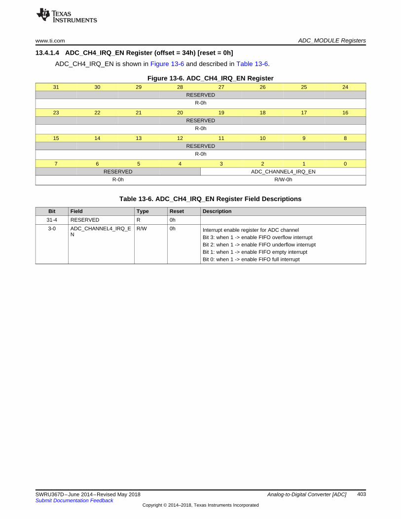
www.ti.com ADC_MODULE Registers
403SWRU367D–June 2014–Revised May 2018Submit Documentation Feedback
Copyright © 2014–2018, Texas Instruments Incorporated
Analog-to-Digital Converter [ADC]
13.4.1.4 ADC_CH4_IRQ_EN Register (offset = 34h) [reset = 0h]ADC_CH4_IRQ_EN is shown in Figure 13-6 and described in Table 13-6.
Figure 13-6. ADC_CH4_IRQ_EN Register31 30 29 28 27 26 25 24
RESERVEDR-0h
23 22 21 20 19 18 17 16RESERVED
R-0h
15 14 13 12 11 10 9 8RESERVED
R-0h
7 6 5 4 3 2 1 0RESERVED ADC_CHANNEL4_IRQ_EN
R-0h R/W-0h
Table 13-6. ADC_CH4_IRQ_EN Register Field Descriptions
Bit Field Type Reset Description31-4 RESERVED R 0h3-0 ADC_CHANNEL4_IRQ_E
NR/W 0h Interrupt enable register for ADC channel
Bit 3: when 1 -> enable FIFO overflow interruptBit 2: when 1 -> enable FIFO underflow interruptBit 1: when 1 -> enable FIFO empty interruptBit 0: when 1 -> enable FIFO full interrupt
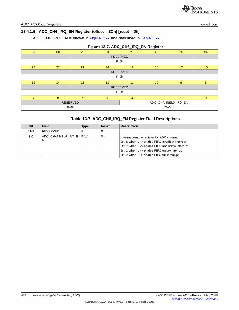
ADC_MODULE Registers www.ti.com
404 SWRU367D–June 2014–Revised May 2018Submit Documentation Feedback
Copyright © 2014–2018, Texas Instruments Incorporated
Analog-to-Digital Converter [ADC]
13.4.1.5 ADC_CH6_IRQ_EN Register (offset = 3Ch) [reset = 0h]ADC_CH6_IRQ_EN is shown in Figure 13-7 and described in Table 13-7.
Figure 13-7. ADC_CH6_IRQ_EN Register31 30 29 28 27 26 25 24
RESERVEDR-0h
23 22 21 20 19 18 17 16RESERVED
R-0h
15 14 13 12 11 10 9 8RESERVED
R-0h
7 6 5 4 3 2 1 0RESERVED ADC_CHANNEL6_IRQ_EN
R-0h R/W-0h
Table 13-7. ADC_CH6_IRQ_EN Register Field Descriptions
Bit Field Type Reset Description31-4 RESERVED R 0h3-0 ADC_CHANNEL6_IRQ_E
NR/W 0h Interrupt enable register for ADC channel
Bit 3: when 1 -> enable FIFO overflow interruptBit 2: when 1 -> enable FIFO underflow interruptBit 1: when 1 -> enable FIFO empty interruptBit 0: when 1 -> enable FIFO full interrupt

www.ti.com ADC_MODULE Registers
405SWRU367D–June 2014–Revised May 2018Submit Documentation Feedback
Copyright © 2014–2018, Texas Instruments Incorporated
Analog-to-Digital Converter [ADC]
13.4.1.6 ADC_CH0_IRQ_STATUS Register (offset = 44h) [reset = 0h]ADC_CH0_IRQ_STATUS is shown in Figure 13-8 and described in Table 13-8.
Figure 13-8. ADC_CH0_IRQ_STATUS Register31 30 29 28 27 26 25 24
RESERVEDR-0h
23 22 21 20 19 18 17 16RESERVED
R-0h
15 14 13 12 11 10 9 8RESERVED
R-0h
7 6 5 4 3 2 1 0RESERVED ADC_CHANNEL0_IRQ_STATUS
R-0h R/W-0h
Table 13-8. ADC_CH0_IRQ_STATUS Register Field Descriptions
Bit Field Type Reset Description31-4 RESERVED R 0h3-0 ADC_CHANNEL0_IRQ_S
TATUSR/W 0h Interrupt status register for ADC channel. Interrupt status can be
cleared on write.Bit 3: when value 1 is written -> Clears FIFO overflow interrupt statusin the next cycle. If same interrupt is set in the same cycle, then theinterrupt would be set and the clear command ignored.Bit 2: when value 1 is written -> Clears FIFO underflow interruptstatus in the next cycle.Bit 1: when value 1 is written -> Clears FIFO empty interrupt statusin the next cycle.Bit 0: when value 1 is written -> Clears FIFO full interrupt status inthe next cycle.

ADC_MODULE Registers www.ti.com
406 SWRU367D–June 2014–Revised May 2018Submit Documentation Feedback
Copyright © 2014–2018, Texas Instruments Incorporated
Analog-to-Digital Converter [ADC]
13.4.1.7 ADC_CH2_IRQ_STATUS Register (offset = 4Ch) [reset = 0h]ADC_CH2_IRQ_STATUS is shown in Figure 13-9 and described in Table 13-9.
Figure 13-9. ADC_CH2_IRQ_STATUS Register31 30 29 28 27 26 25 24
RESERVEDR-0h
23 22 21 20 19 18 17 16RESERVED
R-0h
15 14 13 12 11 10 9 8RESERVED
R-0h
7 6 5 4 3 2 1 0RESERVED ADC_CHANNEL2_IRQ_STATUS
R-0h R/W-0h
Table 13-9. ADC_CH2_IRQ_STATUS Register Field Descriptions
Bit Field Type Reset Description31-4 RESERVED R 0h3-0 ADC_CHANNEL2_IRQ_S
TATUSR/W 0h Interrupt status register for ADC channel. Interrupt status can be
cleared on write.Bit 3: when value 1 is written -> Clears FIFO overflow interrupt statusin the next cycle. If the same interrupt is set in the same cycle, thenthe interrupt would be set and the clear command ignored.Bit 2: when value 1 is written -> Clears FIFO underflow interruptstatus in the next cycle.Bit 1: when value 1 is written -> Clears FIFO empty interrupt statusin the next cycle.Bit 0: when value 1 is written -> Clears FIFO full interrupt status inthe next cycle.
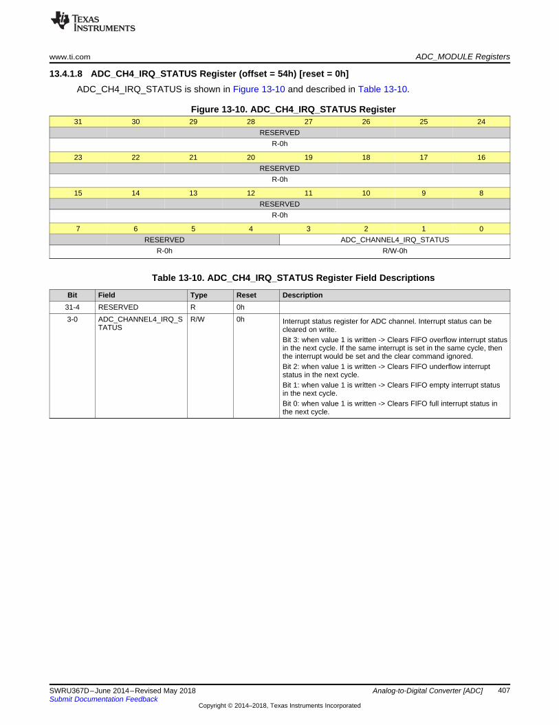
www.ti.com ADC_MODULE Registers
407SWRU367D–June 2014–Revised May 2018Submit Documentation Feedback
Copyright © 2014–2018, Texas Instruments Incorporated
Analog-to-Digital Converter [ADC]
13.4.1.8 ADC_CH4_IRQ_STATUS Register (offset = 54h) [reset = 0h]ADC_CH4_IRQ_STATUS is shown in Figure 13-10 and described in Table 13-10.
Figure 13-10. ADC_CH4_IRQ_STATUS Register31 30 29 28 27 26 25 24
RESERVEDR-0h
23 22 21 20 19 18 17 16RESERVED
R-0h
15 14 13 12 11 10 9 8RESERVED
R-0h
7 6 5 4 3 2 1 0RESERVED ADC_CHANNEL4_IRQ_STATUS
R-0h R/W-0h
Table 13-10. ADC_CH4_IRQ_STATUS Register Field Descriptions
Bit Field Type Reset Description31-4 RESERVED R 0h3-0 ADC_CHANNEL4_IRQ_S
TATUSR/W 0h Interrupt status register for ADC channel. Interrupt status can be
cleared on write.Bit 3: when value 1 is written -> Clears FIFO overflow interrupt statusin the next cycle. If the same interrupt is set in the same cycle, thenthe interrupt would be set and the clear command ignored.Bit 2: when value 1 is written -> Clears FIFO underflow interruptstatus in the next cycle.Bit 1: when value 1 is written -> Clears FIFO empty interrupt statusin the next cycle.Bit 0: when value 1 is written -> Clears FIFO full interrupt status inthe next cycle.
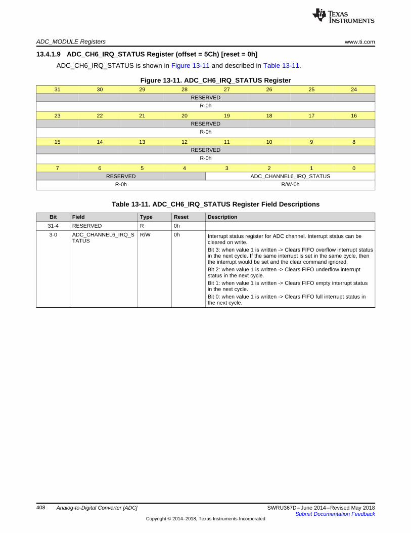
ADC_MODULE Registers www.ti.com
408 SWRU367D–June 2014–Revised May 2018Submit Documentation Feedback
Copyright © 2014–2018, Texas Instruments Incorporated
Analog-to-Digital Converter [ADC]
13.4.1.9 ADC_CH6_IRQ_STATUS Register (offset = 5Ch) [reset = 0h]ADC_CH6_IRQ_STATUS is shown in Figure 13-11 and described in Table 13-11.
Figure 13-11. ADC_CH6_IRQ_STATUS Register31 30 29 28 27 26 25 24
RESERVEDR-0h
23 22 21 20 19 18 17 16RESERVED
R-0h
15 14 13 12 11 10 9 8RESERVED
R-0h
7 6 5 4 3 2 1 0RESERVED ADC_CHANNEL6_IRQ_STATUS
R-0h R/W-0h
Table 13-11. ADC_CH6_IRQ_STATUS Register Field Descriptions
Bit Field Type Reset Description31-4 RESERVED R 0h3-0 ADC_CHANNEL6_IRQ_S
TATUSR/W 0h Interrupt status register for ADC channel. Interrupt status can be
cleared on write.Bit 3: when value 1 is written -> Clears FIFO overflow interrupt statusin the next cycle. If the same interrupt is set in the same cycle, thenthe interrupt would be set and the clear command ignored.Bit 2: when value 1 is written -> Clears FIFO underflow interruptstatus in the next cycle.Bit 1: when value 1 is written -> Clears FIFO empty interrupt statusin the next cycle.Bit 0: when value 1 is written -> Clears FIFO full interrupt status inthe next cycle.
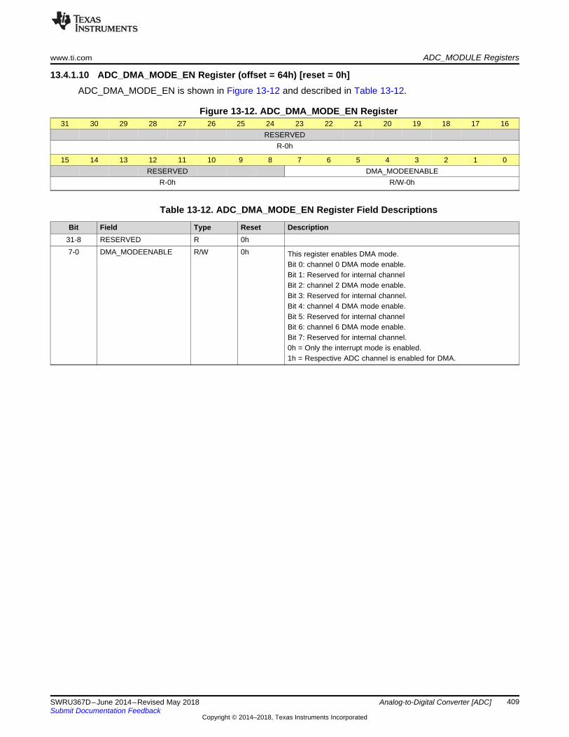
www.ti.com ADC_MODULE Registers
409SWRU367D–June 2014–Revised May 2018Submit Documentation Feedback
Copyright © 2014–2018, Texas Instruments Incorporated
Analog-to-Digital Converter [ADC]
13.4.1.10 ADC_DMA_MODE_EN Register (offset = 64h) [reset = 0h]ADC_DMA_MODE_EN is shown in Figure 13-12 and described in Table 13-12.
Figure 13-12. ADC_DMA_MODE_EN Register31 30 29 28 27 26 25 24 23 22 21 20 19 18 17 16
RESERVEDR-0h
15 14 13 12 11 10 9 8 7 6 5 4 3 2 1 0RESERVED DMA_MODEENABLE
R-0h R/W-0h
Table 13-12. ADC_DMA_MODE_EN Register Field Descriptions
Bit Field Type Reset Description31-8 RESERVED R 0h7-0 DMA_MODEENABLE R/W 0h This register enables DMA mode.
Bit 0: channel 0 DMA mode enable.Bit 1: Reserved for internal channelBit 2: channel 2 DMA mode enable.Bit 3: Reserved for internal channel.Bit 4: channel 4 DMA mode enable.Bit 5: Reserved for internal channelBit 6: channel 6 DMA mode enable.Bit 7: Reserved for internal channel.0h = Only the interrupt mode is enabled.1h = Respective ADC channel is enabled for DMA.
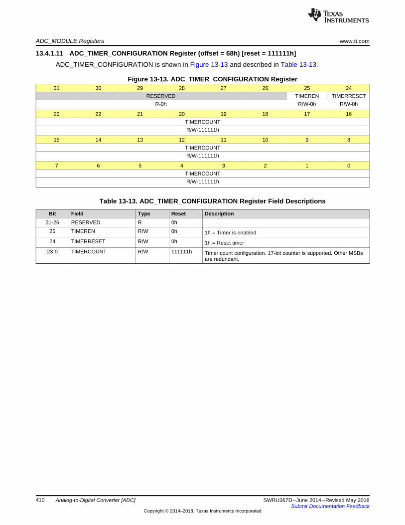
ADC_MODULE Registers www.ti.com
410 SWRU367D–June 2014–Revised May 2018Submit Documentation Feedback
Copyright © 2014–2018, Texas Instruments Incorporated
Analog-to-Digital Converter [ADC]
13.4.1.11 ADC_TIMER_CONFIGURATION Register (offset = 68h) [reset = 111111h]ADC_TIMER_CONFIGURATION is shown in Figure 13-13 and described in Table 13-13.
Figure 13-13. ADC_TIMER_CONFIGURATION Register31 30 29 28 27 26 25 24
RESERVED TIMEREN TIMERRESETR-0h R/W-0h R/W-0h
23 22 21 20 19 18 17 16TIMERCOUNTR/W-111111h
15 14 13 12 11 10 9 8TIMERCOUNTR/W-111111h
7 6 5 4 3 2 1 0TIMERCOUNTR/W-111111h
Table 13-13. ADC_TIMER_CONFIGURATION Register Field Descriptions
Bit Field Type Reset Description31-26 RESERVED R 0h
25 TIMEREN R/W 0h 1h = Timer is enabled24 TIMERRESET R/W 0h 1h = Reset timer
23-0 TIMERCOUNT R/W 111111h Timer count configuration. 17-bit counter is supported. Other MSBsare redundant.
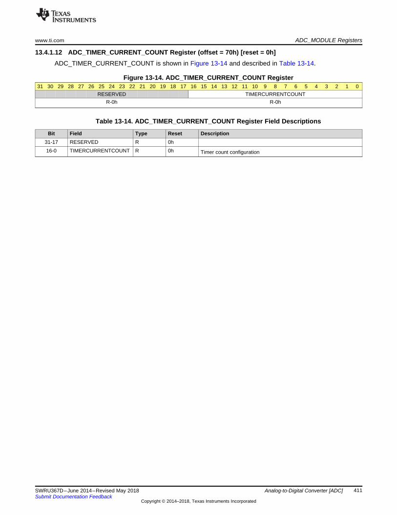
www.ti.com ADC_MODULE Registers
411SWRU367D–June 2014–Revised May 2018Submit Documentation Feedback
Copyright © 2014–2018, Texas Instruments Incorporated
Analog-to-Digital Converter [ADC]
13.4.1.12 ADC_TIMER_CURRENT_COUNT Register (offset = 70h) [reset = 0h]ADC_TIMER_CURRENT_COUNT is shown in Figure 13-14 and described in Table 13-14.
Figure 13-14. ADC_TIMER_CURRENT_COUNT Register31 30 29 28 27 26 25 24 23 22 21 20 19 18 17 16 15 14 13 12 11 10 9 8 7 6 5 4 3 2 1 0
RESERVED TIMERCURRENTCOUNTR-0h R-0h
Table 13-14. ADC_TIMER_CURRENT_COUNT Register Field Descriptions
Bit Field Type Reset Description31-17 RESERVED R 0h16-0 TIMERCURRENTCOUNT R 0h Timer count configuration
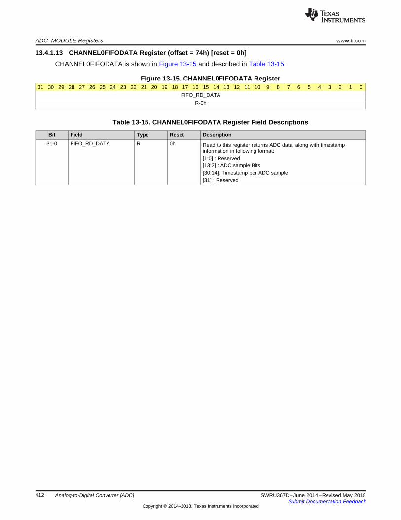
ADC_MODULE Registers www.ti.com
412 SWRU367D–June 2014–Revised May 2018Submit Documentation Feedback
Copyright © 2014–2018, Texas Instruments Incorporated
Analog-to-Digital Converter [ADC]
13.4.1.13 CHANNEL0FIFODATA Register (offset = 74h) [reset = 0h]CHANNEL0FIFODATA is shown in Figure 13-15 and described in Table 13-15.
Figure 13-15. CHANNEL0FIFODATA Register31 30 29 28 27 26 25 24 23 22 21 20 19 18 17 16 15 14 13 12 11 10 9 8 7 6 5 4 3 2 1 0
FIFO_RD_DATAR-0h
Table 13-15. CHANNEL0FIFODATA Register Field Descriptions
Bit Field Type Reset Description31-0 FIFO_RD_DATA R 0h Read to this register returns ADC data, along with timestamp
information in following format:[1:0] : Reserved[13:2] : ADC sample Bits[30:14]: Timestamp per ADC sample[31] : Reserved

www.ti.com ADC_MODULE Registers
413SWRU367D–June 2014–Revised May 2018Submit Documentation Feedback
Copyright © 2014–2018, Texas Instruments Incorporated
Analog-to-Digital Converter [ADC]
13.4.1.14 CHANNEL2FIFODATA Register (offset = 7Ch) [reset = 0h]CHANNEL2FIFODATA is shown in Figure 13-16 and described in Table 13-16.
Figure 13-16. CHANNEL2FIFODATA Register31 30 29 28 27 26 25 24 23 22 21 20 19 18 17 16 15 14 13 12 11 10 9 8 7 6 5 4 3 2 1 0
FIFO_RD_DATAR-0h
Table 13-16. CHANNEL2FIFODATA Register Field Descriptions
Bit Field Type Reset Description31-0 FIFO_RD_DATA R 0h Read to this register returns ADC data, along with timestamp
information in following format:[1:0] : Reserved[13:2] : ADC sample Bits[30:14]: Timestamp per ADC sample[31] : Reserved

ADC_MODULE Registers www.ti.com
414 SWRU367D–June 2014–Revised May 2018Submit Documentation Feedback
Copyright © 2014–2018, Texas Instruments Incorporated
Analog-to-Digital Converter [ADC]
13.4.1.15 CHANNEL4FIFODATA Register (offset = 84h) [reset = 0h]CHANNEL4FIFODATA is shown in Figure 13-17 and described in Table 13-17.
Figure 13-17. CHANNEL4FIFODATA Register31 30 29 28 27 26 25 24 23 22 21 20 19 18 17 16 15 14 13 12 11 10 9 8 7 6 5 4 3 2 1 0
FIFO_RD_DATAR-0h
Table 13-17. CHANNEL4FIFODATA Register Field Descriptions
Bit Field Type Reset Description31-0 FIFO_RD_DATA R 0h Read to this register returns ADC data, along with timestamp
information in following format:[1:0] : Reserved[13:2] : ADC sample Bits[30:14]: Timestamp per ADC sample[31] : Reserved
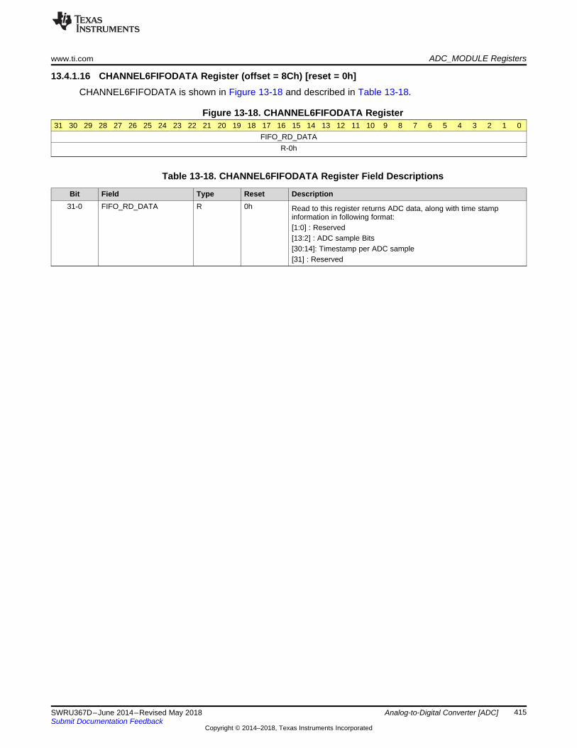
www.ti.com ADC_MODULE Registers
415SWRU367D–June 2014–Revised May 2018Submit Documentation Feedback
Copyright © 2014–2018, Texas Instruments Incorporated
Analog-to-Digital Converter [ADC]
13.4.1.16 CHANNEL6FIFODATA Register (offset = 8Ch) [reset = 0h]CHANNEL6FIFODATA is shown in Figure 13-18 and described in Table 13-18.
Figure 13-18. CHANNEL6FIFODATA Register31 30 29 28 27 26 25 24 23 22 21 20 19 18 17 16 15 14 13 12 11 10 9 8 7 6 5 4 3 2 1 0
FIFO_RD_DATAR-0h
Table 13-18. CHANNEL6FIFODATA Register Field Descriptions
Bit Field Type Reset Description31-0 FIFO_RD_DATA R 0h Read to this register returns ADC data, along with time stamp
information in following format:[1:0] : Reserved[13:2] : ADC sample Bits[30:14]: Timestamp per ADC sample[31] : Reserved
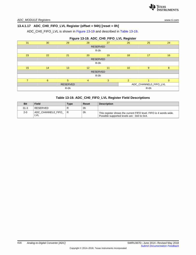
ADC_MODULE Registers www.ti.com
416 SWRU367D–June 2014–Revised May 2018Submit Documentation Feedback
Copyright © 2014–2018, Texas Instruments Incorporated
Analog-to-Digital Converter [ADC]
13.4.1.17 ADC_CH0_FIFO_LVL Register (offset = 94h) [reset = 0h]ADC_CH0_FIFO_LVL is shown in Figure 13-19 and described in Table 13-19.
Figure 13-19. ADC_CH0_FIFO_LVL Register31 30 29 28 27 26 25 24
RESERVEDR-0h
23 22 21 20 19 18 17 16RESERVED
R-0h
15 14 13 12 11 10 9 8RESERVED
R-0h
7 6 5 4 3 2 1 0RESERVED ADC_CHANNEL0_FIFO_LVL
R-0h R-0h
Table 13-19. ADC_CH0_FIFO_LVL Register Field Descriptions
Bit Field Type Reset Description31-3 RESERVED R 0h2-0 ADC_CHANNEL0_FIFO_
LVLR 0h This register shows the current FIFO level. FIFO is 4 words wide.
Possible supported levels are : 0x0 to 0x4.

www.ti.com ADC_MODULE Registers
417SWRU367D–June 2014–Revised May 2018Submit Documentation Feedback
Copyright © 2014–2018, Texas Instruments Incorporated
Analog-to-Digital Converter [ADC]
13.4.1.18 ADC_CH2_FIFO_LVL Register (offset = 9Ch) [reset = 0h]ADC_CH2_FIFO_LVL is shown in Figure 13-20 and described in Table 13-20.
Figure 13-20. ADC_CH2_FIFO_LVL Register31 30 29 28 27 26 25 24
RESERVEDR-0h
23 22 21 20 19 18 17 16RESERVED
R-0h
15 14 13 12 11 10 9 8RESERVED
R-0h
7 6 5 4 3 2 1 0RESERVED ADC_CHANNEL2_FIFO_LVL
R-0h R-0h
Table 13-20. ADC_CH2_FIFO_LVL Register Field Descriptions
Bit Field Type Reset Description31-3 RESERVED R 0h2-0 ADC_CHANNEL2_FIFO_
LVLR 0h This register shows the current FIFO level. FIFO is 4 words wide.
Possible supported levels are : 0x0 to 0x4.
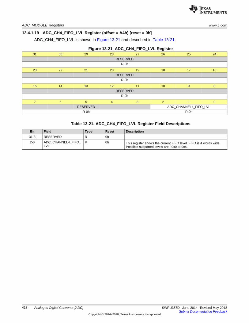
ADC_MODULE Registers www.ti.com
418 SWRU367D–June 2014–Revised May 2018Submit Documentation Feedback
Copyright © 2014–2018, Texas Instruments Incorporated
Analog-to-Digital Converter [ADC]
13.4.1.19 ADC_CH4_FIFO_LVL Register (offset = A4h) [reset = 0h]ADC_CH4_FIFO_LVL is shown in Figure 13-21 and described in Table 13-21.
Figure 13-21. ADC_CH4_FIFO_LVL Register31 30 29 28 27 26 25 24
RESERVEDR-0h
23 22 21 20 19 18 17 16RESERVED
R-0h
15 14 13 12 11 10 9 8RESERVED
R-0h
7 6 5 4 3 2 1 0RESERVED ADC_CHANNEL4_FIFO_LVL
R-0h R-0h
Table 13-21. ADC_CH4_FIFO_LVL Register Field Descriptions
Bit Field Type Reset Description31-3 RESERVED R 0h2-0 ADC_CHANNEL4_FIFO_
LVLR 0h This register shows the current FIFO level. FIFO is 4 words wide.
Possible supported levels are : 0x0 to 0x4.
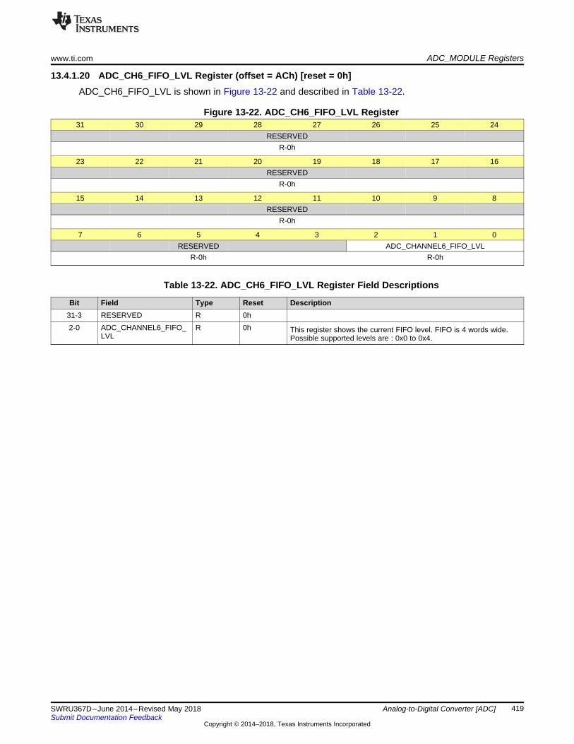
www.ti.com ADC_MODULE Registers
419SWRU367D–June 2014–Revised May 2018Submit Documentation Feedback
Copyright © 2014–2018, Texas Instruments Incorporated
Analog-to-Digital Converter [ADC]
13.4.1.20 ADC_CH6_FIFO_LVL Register (offset = ACh) [reset = 0h]ADC_CH6_FIFO_LVL is shown in Figure 13-22 and described in Table 13-22.
Figure 13-22. ADC_CH6_FIFO_LVL Register31 30 29 28 27 26 25 24
RESERVEDR-0h
23 22 21 20 19 18 17 16RESERVED
R-0h
15 14 13 12 11 10 9 8RESERVED
R-0h
7 6 5 4 3 2 1 0RESERVED ADC_CHANNEL6_FIFO_LVL
R-0h R-0h
Table 13-22. ADC_CH6_FIFO_LVL Register Field Descriptions
Bit Field Type Reset Description31-3 RESERVED R 0h2-0 ADC_CHANNEL6_FIFO_
LVLR 0h This register shows the current FIFO level. FIFO is 4 words wide.
Possible supported levels are : 0x0 to 0x4.
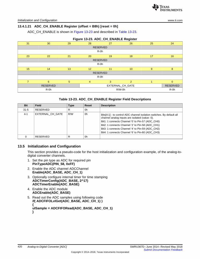
Initialization and Configuration www.ti.com
420 SWRU367D–June 2014–Revised May 2018Submit Documentation Feedback
Copyright © 2014–2018, Texas Instruments Incorporated
Analog-to-Digital Converter [ADC]
13.4.1.21 ADC_CH_ENABLE Register (offset = B8h) [reset = 0h]ADC_CH_ENABLE is shown in Figure 13-23 and described in Table 13-23.
Figure 13-23. ADC_CH_ENABLE Register31 30 29 28 27 26 25 24
RESERVEDR-0h
23 22 21 20 19 18 17 16RESERVED
R-0h
15 14 13 12 11 10 9 8RESERVED
R-0h
7 6 5 4 3 2 1 0RESERVED EXTERNAL_CH_GATE RESERVED
R-0h R/W-0h R-0h
Table 13-23. ADC_CH_ENABLE Register Field Descriptions
Bit Field Type Reset Description31-5 RESERVED R 0h4-1 EXTERNAL_CH_GATE R/W 0h Bits[4:1] : to control ADC channel isolation switches. By default all
channel analog inputs are isolated (value: 0).Bit1: 1 connects Channel '0' to Pin-57 (ADC_CH0)Bit2: 1 connects Channel '2' to Pin-58 (ADC_CH1)Bit3: 1 connects Channel '4' to Pin-59 (ADC_CH2)Bit4: 1 connects Channel '6' to Pin-60 (ADC_CH3)
0 RESERVED R 0h
13.5 Initialization and ConfigurationThis section provides a pseudo-code for the host initialization and configuration example, of the analog-to-digital converter channels.1. Set the pin type as ADC for required pin
PinTypeADC(PIN_58, 0xFF)2. Enable the ADC channel ADCChannel
Enable(ADC_BASE, ADC_CH_1)3. Optionally configure internal timer for time stamping
ADCTimerConfig(ADC_BASE, 2^17)ADCTimerEnable(ADC_BASE)
4. Enable the ADC moduleADCEnable(ADC_BASE)
5. Read out the ADC samples using following codeif( ADCFIFOLvlGet(ADC_BASE, ADC_CH_1) )ulSample = ADCFIFORead(ADC_BASE, ADC_CH_1)
www.ti.com Peripheral Library APIs for ADC Operation
421SWRU367D–June 2014–Revised May 2018Submit Documentation Feedback
Copyright © 2014–2018, Texas Instruments Incorporated
Analog-to-Digital Converter [ADC]
13.6 Peripheral Library APIs for ADC Operation
13.6.1 OverviewFour out of the eight channels of the ADC in the CC3200 are used internally for the SimpleLink subsystem(NWP and Wi-Fi). TI encourages applications to access the four external ADC channels through theperipheral library APIs. These APIs have been designed for optimal ADC operation of the four ADCchannels available to the user, along with the internal ADC channels used for internal functionality of thedevice. In this section, the emphasis is on understanding the ADC APIs provided in the CC3200 SoftwareDevelopment Kit (Peripheral Library). This section lists the software APIs hosted in CC3200 SDK(Peripheral Library) that can be used by the user for easy access to ADC operation.
13.6.2 Configuring the ADC ChannelsConfiguration options for the application developer include:• Enable the channel of interest (assuming the user has programmed the appropriate pins as mentioned
in the device data sheet). Most importantly, the device pin is configured as an analog pin.• Data transfer – CPU (FIFO Level Check and FIFO Read) or DMA• Set up interrupts• Set up timer for time-stamping samples
The following tables serve as a reference for values used for ulChannel and ulIntFlags:
Table 13-24. ulChannel Tags
Tag ValueADC_CH_0 0x00000000ADC_CH_1 0x00000008ADC_CH_2 0x00000010ADC_CH_3 0x00000018
Table 13-25. ulIntFlags Tags
Tag ValueADC_DMA_DONE 0x00000010ADC_FIFO_OVERFLOW 0x00000008ADC_FIFO_UNDERFLOW 0x00000004ADC_FIFO_EMPTY 0x00000002ADC_FIFO_FULL 0x00000001
13.6.3 Basic APIs for Enabling and Configuring the Interface
13.6.3.1 void ADCEnable (unsigned long ulBase)Enables the ADC.
Parameters:
ulBase Base address of the ADC
Peripheral Library APIs for ADC Operation www.ti.com
422 SWRU367D–June 2014–Revised May 2018Submit Documentation Feedback
Copyright © 2014–2018, Texas Instruments Incorporated
Analog-to-Digital Converter [ADC]
This function sets the ADC global enable.
Returns:• None
13.6.3.2 void ADCDisable (unsigned long ulBase)Disables the ADC.
Parameters:
ulBase Base address of the ADC
This function clears the ADC global enable.
Returns:• None
13.6.3.3 void ADCChannelEnable (unsigned long ulBase, unsigned long ulChannel)Enables a specified ADC channel.
Parameters:
ulBase Base address of the ADCulChannel One of the valid ADC channels
This function enables specified ADC channel and configures the pin as an analog pin.
Returns:• None
13.6.3.4 void ADCChannelDisable (unsigned long ulBase, unsigned long ulChannel)Disables a specified ADC channel.
Parameters:
ulBase Base address of the ADCulChannel One of the valid ADC channels
This function disables a specified ADC channel.
Returns:• None
13.6.4 APIs for Data Transfer [Direct Access to FIFO and DMA Setup]
13.6.4.1 unsigned char ADCFIFOLvlGet (unsigned long ulBase, unsigned long ulChannel)Gets the current FIFO level for a specified ADC channel.
Parameters:
ulBase Base address of the ADCulChannel One of the valid ADC channels
www.ti.com Peripheral Library APIs for ADC Operation
423SWRU367D–June 2014–Revised May 2018Submit Documentation Feedback
Copyright © 2014–2018, Texas Instruments Incorporated
Analog-to-Digital Converter [ADC]
This function returns the current FIFO level for specified ADC channel.
The ulChannel parameter should be one of:• ADC_CH_0 for channel 0• ADC_CH_1 for channel 1• ADC_CH_2 for channel 2• ADC_CH_3 for channel 3
Returns:• Returns the current FIFO level for a specified channel.
13.6.4.2 unsigned long ADCFIFORead (unsigned long ulBase, unsigned long ulChannel)Reads FIFO for a specified ADC channel.
Parameters:
ulBase Base address of the ADCulChannel One of the valid ADC channels
This function returns one data sample from the channel FIFO as specified by the ulChannel parameter.
The ulChannel parameter should be one of:• ADC_CH_0 for channel 0• ADC_CH_1 for channel 1• ADC_CH_2 for channel 2• ADC_CH_3 for channel 3
Returns:• Returns one data sample from the channel FIFO.
13.6.4.3 void ADCDMAEnable (unsigned long ulBase, unsigned long ulChannel)Enables the ADC DMA operation for a specified channel.
Parameters:
ulBase Base address of the ADCulChannel One of the valid ADC channels
This function enables the DMA operation for a specified ADC channel.
The ulChannel parameter should be one of:• ADC_CH_0 for channel 0• ADC_CH_1 for channel 1• ADC_CH_2 for channel 2• ADC_CH_3 for channel 3
Returns:• None.
13.6.4.4 void ADCDMADisable (unsigned long ulBase, unsigned long ulChannel)Disables the ADC DMA operation for a specified channel.
Parameters:
Peripheral Library APIs for ADC Operation www.ti.com
424 SWRU367D–June 2014–Revised May 2018Submit Documentation Feedback
Copyright © 2014–2018, Texas Instruments Incorporated
Analog-to-Digital Converter [ADC]
ulBase Base address of the ADCulChannel One of the valid ADC channels
This function disables the DMA operation for a specified ADC channel.
The ulChannel parameter should be one of:• ADC_CH_0 for channel 0• ADC_CH_1 for channel 1• ADC_CH_2 for channel 2• ADC_CH_3 for channel 3
Returns:• None.
13.6.5 APIs for Interrupt Usage
13.6.5.1 void ADCIntEnable (unsigned long ulBase, unsigned long ulChannel, unsigned long ulIntFlags)Enables individual interrupt sources for a specified channel.
Parameters:
ulBase Base address of the ADCulChannel One of the valid ADC channelsulIntFlags The bit mask of the interrupt sources to be enabled
This function enables the indicated ADC interrupt sources. Only enabled sources can be reflected to theprocessor interrupt; disabled sources have no effect on the processor.
The ulChannel parameter should be one of:• ADC_CH_0 for channel 0• ADC_CH_1 for channel 1• ADC_CH_2 for channel 2• ADC_CH_3 for channel 3
The ulIntFlags parameter is the logical OR of any of:• ADC_DMA_DONE for DMA done• ADC_FIFO_OVERFLOW for FIFO over flow• ADC_FIFO_UNDERFLOW for FIFO under flow• ADC_FIFO_EMPTY for FIFO empty• ADC_FIFO_FULL for FIFO full
Returns:• None
13.6.5.2 void ADCIntDisable (unsigned long ulBase, unsigned long ulChannel, unsigned long ulIntFlags)Disables individual interrupt sources for a specified channel.
Parameters:
ulBase Base address of the ADCulChannel One of the valid ADC channelsulIntFlags The bit mask of the interrupt sources to be enabled
www.ti.com Peripheral Library APIs for ADC Operation
425SWRU367D–June 2014–Revised May 2018Submit Documentation Feedback
Copyright © 2014–2018, Texas Instruments Incorporated
Analog-to-Digital Converter [ADC]
This function disables the indicated ADC interrupt sources. Only enabled sources can be reflected to theprocessor interrupt; disabled sources have no effect on the processor.
The ulIntFlags and ulChannel parameters should be as explained in ADCIntEnable().
Returns:• None
13.6.5.3 void ADCIntRegister (unsigned long ulBase, unsigned long ulChannel, void(*)(void) pfnHandler)Enables and registers ADC interrupt handler for a specified channel.
Parameters:
ulBase Base address of the ADCulChannel One of the valid ADC channelspfnHandler A pointer to the function to be called when the ADC channel interrupt occurs
This function enables and registers ADC interrupt handler for a specified channel. An individual interruptfor each channel should be enabled using ADCIntEnable(). It is the responsibility of the interrupt handlerto clear the interrupt source.
The ulChannel parameter should be one of:• ADC_CH_0 for channel 0• ADC_CH_1 for channel 1• ADC_CH_2 for channel 2• ADC_CH_3 for channel 3
Returns:• None
13.6.5.4 void ADCIntUnregister (unsigned long ulBase, unsigned long ulChannel)Disables and unregisters ADC interrupt handler for a specified channel.
Parameters:
ulBase Base address of the ADCulChannel One of the valid ADC channels
This function disables and unregisters ADC interrupt handler for a specified channel. This function alsomasks off the interrupt in the interrupt controller, so that the interrupt handler is no longer called.
The ulChannel parameter should be one of:• ADC_CH_0 for channel 0• ADC_CH_1 for channel 1• ADC_CH_2 for channel 2• ADC_CH_3 for channel 3
Returns:• None
13.6.5.5 unsigned long ADCIntStatus (unsigned long ulBase, unsigned long ulChannel)Gets the current channel interrupt status.
Parameters:
Peripheral Library APIs for ADC Operation www.ti.com
426 SWRU367D–June 2014–Revised May 2018Submit Documentation Feedback
Copyright © 2014–2018, Texas Instruments Incorporated
Analog-to-Digital Converter [ADC]
ulBase Base address of the ADCulChannel One of the valid ADC channels
This function returns the interrupt status of the specified ADC channel. See Table 13-25
The parameter ulChannel should be as explained in ADCIntEnable().
Returns:• Return the ADC channel interrupt status, enumerated as a bit field of values described in
ADCIntEnable()
13.6.5.6 void ADCIntClear (unsigned long ulBase, unsigned long ulChannel, unsigned long ulIntFlags)Clears the current channel interrupt sources.
Parameters:
ulBase Base address of the ADCulChannel One of the valid ADC channelsulIntFlags Bit mask of the interrupt sources to be cleared
This function clears an individual interrupt source for the specified ADC channel.
The ulChannel parameter should be as explained in ADCIntEnable().
Returns:• None
13.6.6 APIs for Setting Up ADC Timer for Time Stamping the Samples
13.6.6.1 void ADCTimerConfig (unsigned long ulBase, unsigned long ulValue)Configures the ADC internal timer.
Parameters:
ulBase Base address of the ADCulValue Wrap-around value of the timer
This function configures the ADC internal timer. The ADC timer is 17-bit timer that internally time-stampsthe ADC data samples. The user can read the timestamp, along with the sample, from the FIFO registers.Each sample in the FIFO contains 14-bit actual data and an 18-bit timestamp.
The ulValue parameter can take any value between 0 and 2^17.
Returns:• None
13.6.6.2 void ADCTimerDisable (unsigned long ulBase)Disables the ADC internal timer.
Parameters:
ulBase Base address of the ADC
www.ti.com Peripheral Library APIs for ADC Operation
427SWRU367D–June 2014–Revised May 2018Submit Documentation Feedback
Copyright © 2014–2018, Texas Instruments Incorporated
Analog-to-Digital Converter [ADC]
This function disables the 17-bit ADC internal timer.
Returns:• None
13.6.6.3 void ADCTimerEnable (unsigned long ulBase)Enables the ADC internal timer.
Parameters:
ulBase Base address of the ADC
This function enables the 17-bit ADC internal timer.
Returns:• None
13.6.6.4 void ADCTimerReset (unsigned long ulBase)Resets the ADC internal timer.
Parameters:
ulBase Base address of the ADC
This function resets the 17-bit ADC internal timer.
Returns:• None
13.6.6.5 unsigned long ADCTimerValueGet (unsigned long ulBase)Gets the current value of ADC internal timer.
Parameters:
ulBase Base address of the ADC
This function gets the current value of the 17-bit ADC internal timer.
Returns:• Returns the current value of the ADC internal timer.
428 SWRU367D–June 2014–Revised May 2018Submit Documentation Feedback
Copyright © 2014–2018, Texas Instruments Incorporated
Parallel Camera Interface Module
Chapter 14SWRU367D–June 2014–Revised May 2018
Parallel Camera Interface Module
Topic ........................................................................................................................... Page
14.1 Overview ......................................................................................................... 42914.2 Image Sensor Interface ..................................................................................... 42914.3 Functional Description ...................................................................................... 43014.4 Programming Model.......................................................................................... 43414.5 Interrupt Handling............................................................................................. 43514.6 Camera Interface Module Functional Registers .................................................... 43614.7 Developer’s Guide ............................................................................................ 450
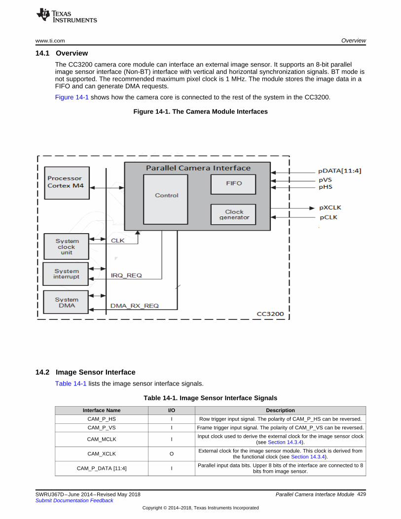
www.ti.com Overview
429SWRU367D–June 2014–Revised May 2018Submit Documentation Feedback
Copyright © 2014–2018, Texas Instruments Incorporated
Parallel Camera Interface Module
14.1 OverviewThe CC3200 camera core module can interface an external image sensor. It supports an 8-bit parallelimage sensor interface (Non-BT) interface with vertical and horizontal synchronization signals. BT mode isnot supported. The recommended maximum pixel clock is 1 MHz. The module stores the image data in aFIFO and can generate DMA requests.
Figure 14-1 shows how the camera core is connected to the rest of the system in the CC3200.
Figure 14-1. The Camera Module Interfaces
14.2 Image Sensor InterfaceTable 14-1 lists the image sensor interface signals.
Table 14-1. Image Sensor Interface Signals
Interface Name I/O DescriptionCAM_P_HS I Row trigger input signal. The polarity of CAM_P_HS can be reversed.CAM_P_VS I Frame trigger input signal. The polarity of CAM_P_VS can be reversed.
CAM_MCLK I Input clock used to derive the external clock for the image sensor clock(see Section 14.3.4).
CAM_XCLK O External clock for the image sensor module. This clock is derived fromthe functional clock (see Section 14.3.4).
CAM_P_DATA [11:4] I Parallel input data bits. Upper 8 bits of the interface are connected to 8bits from image sensor.
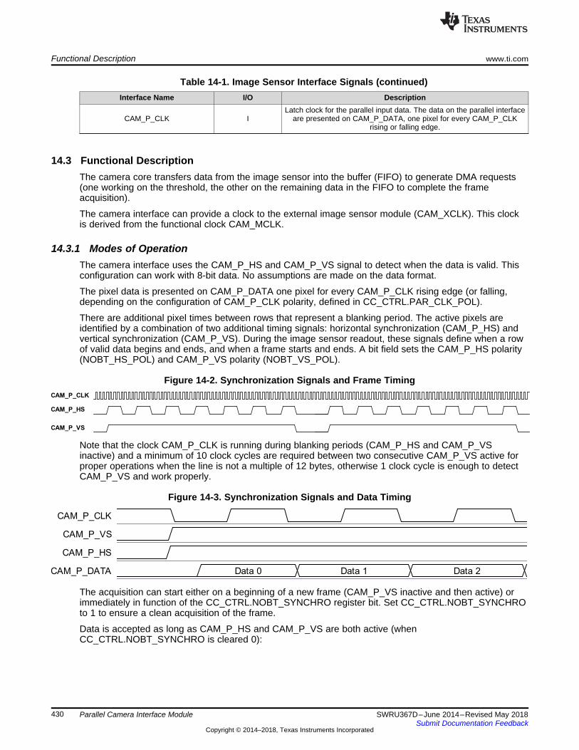
Functional Description www.ti.com
430 SWRU367D–June 2014–Revised May 2018Submit Documentation Feedback
Copyright © 2014–2018, Texas Instruments Incorporated
Parallel Camera Interface Module
Table 14-1. Image Sensor Interface Signals (continued)Interface Name I/O Description
CAM_P_CLK ILatch clock for the parallel input data. The data on the parallel interface
are presented on CAM_P_DATA, one pixel for every CAM_P_CLKrising or falling edge.
14.3 Functional DescriptionThe camera core transfers data from the image sensor into the buffer (FIFO) to generate DMA requests(one working on the threshold, the other on the remaining data in the FIFO to complete the frameacquisition).
The camera interface can provide a clock to the external image sensor module (CAM_XCLK). This clockis derived from the functional clock CAM_MCLK.
14.3.1 Modes of OperationThe camera interface uses the CAM_P_HS and CAM_P_VS signal to detect when the data is valid. Thisconfiguration can work with 8-bit data. No assumptions are made on the data format.
The pixel data is presented on CAM_P_DATA one pixel for every CAM_P_CLK rising edge (or falling,depending on the configuration of CAM_P_CLK polarity, defined in CC_CTRL.PAR_CLK_POL).
There are additional pixel times between rows that represent a blanking period. The active pixels areidentified by a combination of two additional timing signals: horizontal synchronization (CAM_P_HS) andvertical synchronization (CAM_P_VS). During the image sensor readout, these signals define when a rowof valid data begins and ends, and when a frame starts and ends. A bit field sets the CAM_P_HS polarity(NOBT_HS_POL) and CAM_P_VS polarity (NOBT_VS_POL).
Figure 14-2. Synchronization Signals and Frame Timing
Note that the clock CAM_P_CLK is running during blanking periods (CAM_P_HS and CAM_P_VSinactive) and a minimum of 10 clock cycles are required between two consecutive CAM_P_VS active forproper operations when the line is not a multiple of 12 bytes, otherwise 1 clock cycle is enough to detectCAM_P_VS and work properly.
Figure 14-3. Synchronization Signals and Data Timing
The acquisition can start either on a beginning of a new frame (CAM_P_VS inactive and then active) orimmediately in function of the CC_CTRL.NOBT_SYNCHRO register bit. Set CC_CTRL.NOBT_SYNCHROto 1 to ensure a clean acquisition of the frame.
Data is accepted as long as CAM_P_HS and CAM_P_VS are both active (whenCC_CTRL.NOBT_SYNCHRO is cleared 0):
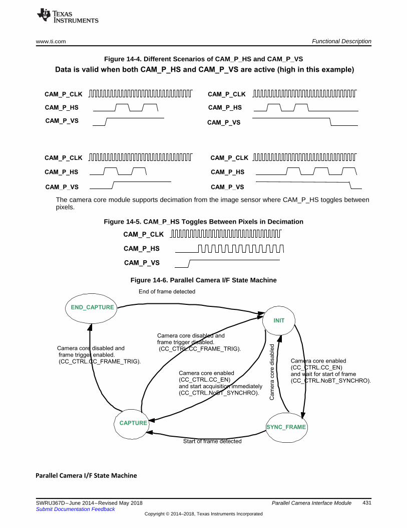
www.ti.com Functional Description
431SWRU367D–June 2014–Revised May 2018Submit Documentation Feedback
Copyright © 2014–2018, Texas Instruments Incorporated
Parallel Camera Interface Module
Figure 14-4. Different Scenarios of CAM_P_HS and CAM_P_VS
The camera core module supports decimation from the image sensor where CAM_P_HS toggles betweenpixels.
Figure 14-5. CAM_P_HS Toggles Between Pixels in Decimation
Figure 14-6. Parallel Camera I/F State Machine
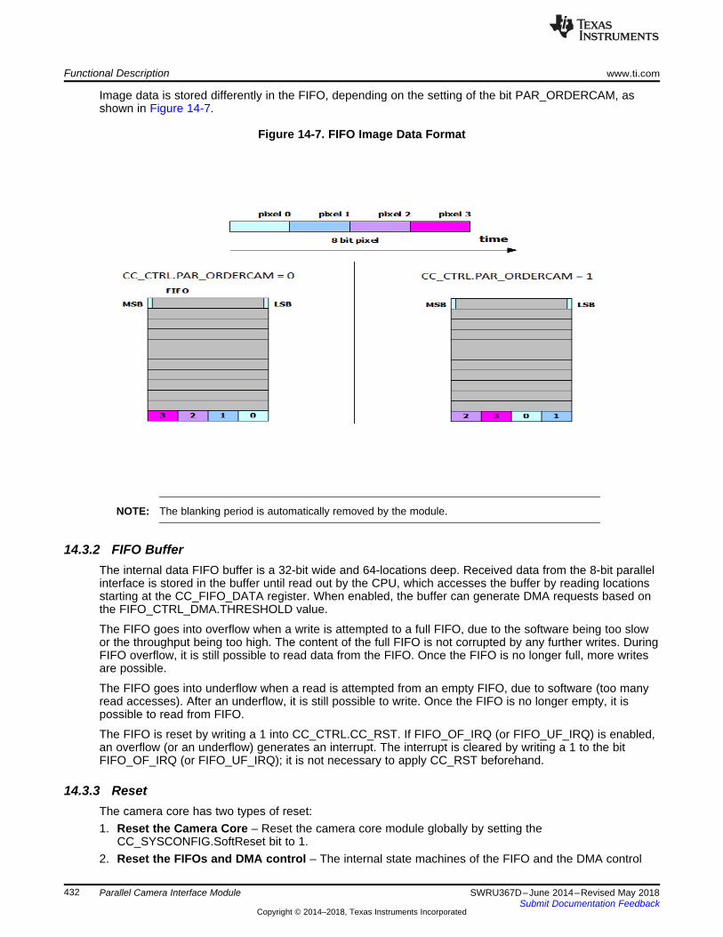
Functional Description www.ti.com
432 SWRU367D–June 2014–Revised May 2018Submit Documentation Feedback
Copyright © 2014–2018, Texas Instruments Incorporated
Parallel Camera Interface Module
Image data is stored differently in the FIFO, depending on the setting of the bit PAR_ORDERCAM, asshown in Figure 14-7.
Figure 14-7. FIFO Image Data Format
NOTE: The blanking period is automatically removed by the module.
14.3.2 FIFO BufferThe internal data FIFO buffer is a 32-bit wide and 64-locations deep. Received data from the 8-bit parallelinterface is stored in the buffer until read out by the CPU, which accesses the buffer by reading locationsstarting at the CC_FIFO_DATA register. When enabled, the buffer can generate DMA requests based onthe FIFO_CTRL_DMA.THRESHOLD value.
The FIFO goes into overflow when a write is attempted to a full FIFO, due to the software being too slowor the throughput being too high. The content of the full FIFO is not corrupted by any further writes. DuringFIFO overflow, it is still possible to read data from the FIFO. Once the FIFO is no longer full, more writesare possible.
The FIFO goes into underflow when a read is attempted from an empty FIFO, due to software (too manyread accesses). After an underflow, it is still possible to write. Once the FIFO is no longer empty, it ispossible to read from FIFO.
The FIFO is reset by writing a 1 into CC_CTRL.CC_RST. If FIFO_OF_IRQ (or FIFO_UF_IRQ) is enabled,an overflow (or an underflow) generates an interrupt. The interrupt is cleared by writing a 1 to the bitFIFO_OF_IRQ (or FIFO_UF_IRQ); it is not necessary to apply CC_RST beforehand.
14.3.3 ResetThe camera core has two types of reset:1. Reset the Camera Core – Reset the camera core module globally by setting the
CC_SYSCONFIG.SoftReset bit to 1.2. Reset the FIFOs and DMA control – The internal state machines of the FIFO and the DMA control
www.ti.com Functional Description
433SWRU367D–June 2014–Revised May 2018Submit Documentation Feedback
Copyright © 2014–2018, Texas Instruments Incorporated
Parallel Camera Interface Module
circuitry are reset by setting the CC_CTRL.CC_RST bit to 1. This bit is primarily used after anunderflow or an overflow, to avoid re-configuring the entire module.
14.3.4 Clock GenerationThe module divides down CAM_MCLK and generates CAM_XCLK clock to the external camera sensor.The configuration of the CAM_XCLK divider is programmable by setting the configuration registerCC_CTRL_XCLK.
CAM_XCLK is not used by the camera core module itself. It is routed to the chip pin.
Table 14-2. Ratio of the XCLK Frequency Generator
Ratio XCLK Based on CAM_MCLK ( CAM_MCLK = 120 MHz)0 (default) Stable low level, divider not enabled
1 Stable high level, divider not enabled2 60 MHz (division by 2)3 40 MHz (division by 3)4 30 MHz5 24 MHz6 20 MHz7 17.14 MHz8 15 MHz9 13.3 MHz10 12 MHz11 10.91 MHz12 10 MHz... ...30 4 MHz (division by 30)31 Bypass (CAM_XCLK = CAM_MCLK)
14.3.5 Interrupt GenerationThe interrupt line is asserted (active low) when one the following events takes place:• FIFO_UF – FIFO underflow• FIFO_OF – FIFO overflow• FIFO_THR – FIFO threshold• FIFO_FULL – FIFO full• FIFO_NOEMPTY – FIFO not empty (can be used to detect that a first data is written)• FE – Frame End
When the CC_IRQSTATUS register is read, the register is not automatically reset. To reset the interrupt,write a 1 to the corresponding bit.
Each event that generates an interrupt can be individually enabled using the CC_IRQENABLE. When aparticular event is not enabled (for example CC_IRQENABLE[5] = 0), the corresponding status(CC_IRQSTATUS[5] = 1) bit is flagged if the corresponding event occurs. This has no effect on theinterrupt line, but can be used by the software to poll the status.
14.3.6 DMA InterfaceThe camera core module interfaces with a DMA controller. At the system level, the advantage is todischarge the CPU of the data transfers.
The module can generate a DMA request when the FIFO reaches the threshold programmed intoCC_CTRL_DMA.FIFO_THRESHOLD.
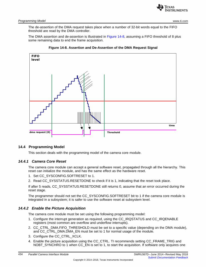
Programming Model www.ti.com
434 SWRU367D–June 2014–Revised May 2018Submit Documentation Feedback
Copyright © 2014–2018, Texas Instruments Incorporated
Parallel Camera Interface Module
The de-assertion of the DMA request takes place when a number of 32-bit words equal to the FIFOthreshold are read by the DMA controller.
The DMA assertion and de-assertion is illustrated in Figure 14-8, assuming a FIFO threshold of 8 plussome remaining data to end the frame acquisition.
Figure 14-8. Assertion and De-Assertion of the DMA Request Signal
14.4 Programming ModelThis section deals with the programming model of the camera core module.
14.4.1 Camera Core ResetThe camera core module can accept a general software reset, propagated through all the hierarchy. Thisreset can initialize the module, and has the same effect as the hardware reset.1. Set CC_SYSCONFIG.SOFTRESET to 1.2. Read CC_SYSSTATUS.RESETDONE to check if it is 1, indicating that the reset took place.
If after 5 reads, CC_SYSSTATUS.RESETDONE still returns 0, assume that an error occurred during thereset stage.
The programmer should not set the CC_SYSCONFIG.SOFTRESET bit to 1 if the camera core module isintegrated in a subsystem; it is safer to use the software reset at subsystem level.
14.4.2 Enable the Picture AcquisitionThe camera core module must be set using the following programming model:1. Configure the interrupt generation as required, using the CC_IRQSTATUS and CC_IRQENABLE
registers (most common are overflow and underflow interrupts).2. CC_CTRL_DMA.FIFO_THRESHOLD must be set to a specific value (depending on the DMA module),
and CC_CTRL_DMA.DMA_EN must be set to 1 for normal usage of the module.3. Configure the CC_CTRL_XCLK.4. Enable the picture acquisition using the CC_CTRL. TI recommends setting CC_FRAME_TRIG and
NOBT_SYNCHRO to 1 when CC_EN is set to 1, to start the acquisition. If software only acquires one
www.ti.com Programming Model
435SWRU367D–June 2014–Revised May 2018Submit Documentation Feedback
Copyright © 2014–2018, Texas Instruments Incorporated
Parallel Camera Interface Module
frame acquisition, use the CC_ONE_SHOT register bit (in this case, the module is automaticallydisabled at the end of the frame).
14.4.3 Disable the Picture AcquisitionTo end the picture acquisition, set the CC_CTRL.CC_EN to 0 in conjunction with settingCC_CTRL.CC_FRAME_TRIG to 1, to properly disable the frame acquisition. In that case, the camera coreends the current frame at the end, or stops immediately if there is no frame ongoing.
14.5 Interrupt Handling
14.5.1 FIFO_OF_IRQ (FIFO overflow)
1. Set CC_CTRL.CC_EN to 0 and CC_CTRL.CC_FRAME_TRIG to 0, thus stopping the data flow fromthe image sensor.
2. Clear the interrupt by writing 1 to the CC_IRQSTATUS.FIFO_OF_IRQ bit.3. If the CC_CTRL_DMA.DMA_EN bit is set to 0, the CPU may keep reading the FIFO_DATA register, or
stop reading. If the CC_CTRL_DMA.EN bit is set to 1, the CPU may stop the DMA, or let it run untilthere are no more DMA requests.
4. Reset FIFO pointers and internal camera core state machines by writing 1 to the CC_CTRL.CC_RSTbit.
5. Set the CC_CTRL.CC_EN bit to 1, to re-enable the data flow from the image sensor.
If an overflow occurs, the entire data flow path must be reset to restart cleanly.
14.5.2 FIFO_UF_IRQ (FIFO underflow)1. Set the CC_CTRL.CC_EN bit to 0 and the CC_CTRL.CC_FRAME_TRIG bit to 0, thus stopping the
data flow from the image sensor.2. Clear the interrupt by writing 1 to the CC_IRQSTATUS.FIFO_UF_IRQ bit.3. Reset FIFO pointers and internal camera core state machines by writing 1 to the CC_CTRL.CC_RST
bit.4. Set the CC_CTRL.CC_EN bit to 1, to re-enable the data flow from the image sensor.
If an underflow occurs, the entire data flow path must be reset to restart cleanly.
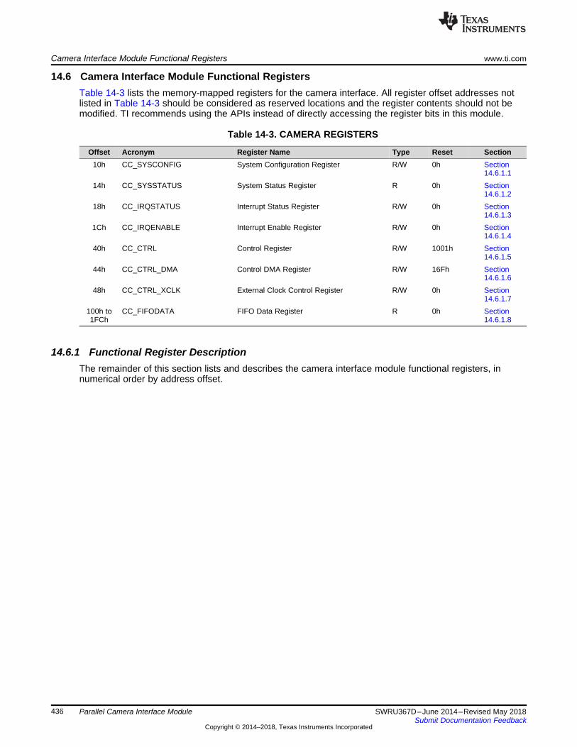
Camera Interface Module Functional Registers www.ti.com
436 SWRU367D–June 2014–Revised May 2018Submit Documentation Feedback
Copyright © 2014–2018, Texas Instruments Incorporated
Parallel Camera Interface Module
14.6 Camera Interface Module Functional RegistersTable 14-3 lists the memory-mapped registers for the camera interface. All register offset addresses notlisted in Table 14-3 should be considered as reserved locations and the register contents should not bemodified. TI recommends using the APIs instead of directly accessing the register bits in this module.
Table 14-3. CAMERA REGISTERS
Offset Acronym Register Name Type Reset Section10h CC_SYSCONFIG System Configuration Register R/W 0h Section
14.6.1.114h CC_SYSSTATUS System Status Register R 0h Section
14.6.1.218h CC_IRQSTATUS Interrupt Status Register R/W 0h Section
14.6.1.31Ch CC_IRQENABLE Interrupt Enable Register R/W 0h Section
14.6.1.440h CC_CTRL Control Register R/W 1001h Section
14.6.1.544h CC_CTRL_DMA Control DMA Register R/W 16Fh Section
14.6.1.648h CC_CTRL_XCLK External Clock Control Register R/W 0h Section
14.6.1.7100h to1FCh
CC_FIFODATA FIFO Data Register R 0h Section14.6.1.8
14.6.1 Functional Register DescriptionThe remainder of this section lists and describes the camera interface module functional registers, innumerical order by address offset.
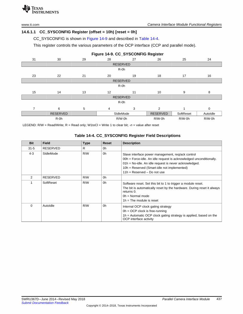
www.ti.com Camera Interface Module Functional Registers
437SWRU367D–June 2014–Revised May 2018Submit Documentation Feedback
Copyright © 2014–2018, Texas Instruments Incorporated
Parallel Camera Interface Module
14.6.1.1 CC_SYSCONFIG Register (offset = 10h) [reset = 0h]CC_SYSCONFIG is shown in Figure 14-9 and described in Table 14-4.
This register controls the various parameters of the OCP interface (CCP and parallel mode).
Figure 14-9. CC_SYSCONFIG Register31 30 29 28 27 26 25 24
RESERVEDR-0h
23 22 21 20 19 18 17 16RESERVED
R-0h
15 14 13 12 11 10 9 8RESERVED
R-0h
7 6 5 4 3 2 1 0RESERVED SIdleMode RESERVED SoftReset AutoIdle
R-0h R/W-0h R/W-0h R/W-0h R/W-0h
LEGEND: R/W = Read/Write; R = Read only; W1toCl = Write 1 to clear bit; -n = value after reset
Table 14-4. CC_SYSCONFIG Register Field Descriptions
Bit Field Type Reset Description31-5 RESERVED R 0h4-3 SIdleMode R/W 0h Slave interface power management, req/ack control
00h = Force-idle. An idle request is acknowledged unconditionally.01h = No-idle. An idle request is never acknowledged.10h = Reserved (Smart-idle not implemented)11h = Reserved – Do not use
2 RESERVED R/W 0h1 SoftReset R/W 0h Software reset. Set this bit to 1 to trigger a module reset.
The bit is automatically reset by the hardware. During reset it alwaysreturns 0.0h = Normal mode1h = The module is reset
0 AutoIdle R/W 0h Internal OCP clock gating strategy0h = OCP clock is free-running1h = Automatic OCP clock gating strategy is applied, based on theOCP interface activity
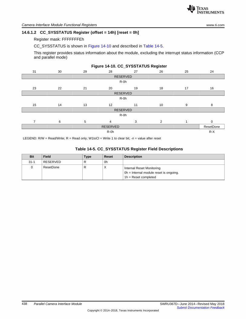
Camera Interface Module Functional Registers www.ti.com
438 SWRU367D–June 2014–Revised May 2018Submit Documentation Feedback
Copyright © 2014–2018, Texas Instruments Incorporated
Parallel Camera Interface Module
14.6.1.2 CC_SYSSTATUS Register (offset = 14h) [reset = 0h]Register mask: FFFFFFFEh
CC_SYSSTATUS is shown in Figure 14-10 and described in Table 14-5.
This register provides status information about the module, excluding the interrupt status information (CCPand parallel mode)
Figure 14-10. CC_SYSSTATUS Register31 30 29 28 27 26 25 24
RESERVEDR-0h
23 22 21 20 19 18 17 16RESERVED
R-0h
15 14 13 12 11 10 9 8RESERVED
R-0h
7 6 5 4 3 2 1 0RESERVED ResetDone
R-0h R-X
LEGEND: R/W = Read/Write; R = Read only; W1toCl = Write 1 to clear bit; -n = value after reset
Table 14-5. CC_SYSSTATUS Register Field Descriptions
Bit Field Type Reset Description31-1 RESERVED R 0h
0 ResetDone R X Internal Reset Monitoring0h = Internal module reset is ongoing.1h = Reset completed
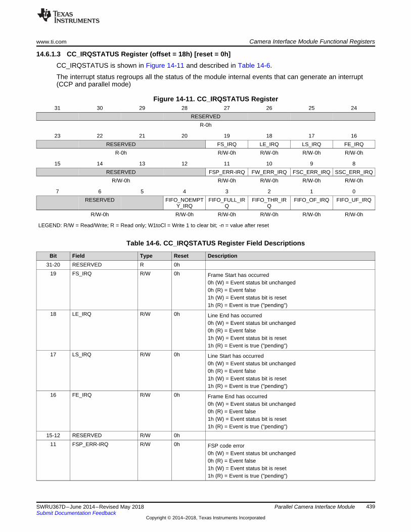
www.ti.com Camera Interface Module Functional Registers
439SWRU367D–June 2014–Revised May 2018Submit Documentation Feedback
Copyright © 2014–2018, Texas Instruments Incorporated
Parallel Camera Interface Module
14.6.1.3 CC_IRQSTATUS Register (offset = 18h) [reset = 0h]CC_IRQSTATUS is shown in Figure 14-11 and described in Table 14-6.
The interrupt status regroups all the status of the module internal events that can generate an interrupt(CCP and parallel mode)
Figure 14-11. CC_IRQSTATUS Register31 30 29 28 27 26 25 24
RESERVEDR-0h
23 22 21 20 19 18 17 16RESERVED FS_IRQ LE_IRQ LS_IRQ FE_IRQ
R-0h R/W-0h R/W-0h R/W-0h R/W-0h
15 14 13 12 11 10 9 8RESERVED FSP_ERR-IRQ FW_ERR_IRQ FSC_ERR_IRQ SSC_ERR_IRQ
R/W-0h R/W-0h R/W-0h R/W-0h R/W-0h
7 6 5 4 3 2 1 0RESERVED FIFO_NOEMPT
Y_IRQFIFO_FULL_IR
QFIFO_THR_IR
QFIFO_OF_IRQ FIFO_UF_IRQ
R/W-0h R/W-0h R/W-0h R/W-0h R/W-0h R/W-0h
LEGEND: R/W = Read/Write; R = Read only; W1toCl = Write 1 to clear bit; -n = value after reset
Table 14-6. CC_IRQSTATUS Register Field Descriptions
Bit Field Type Reset Description31-20 RESERVED R 0h
19 FS_IRQ R/W 0h Frame Start has occurred0h (W) = Event status bit unchanged0h (R) = Event false1h (W) = Event status bit is reset1h (R) = Event is true ("pending")
18 LE_IRQ R/W 0h Line End has occurred0h (W) = Event status bit unchanged0h (R) = Event false1h (W) = Event status bit is reset1h (R) = Event is true ("pending")
17 LS_IRQ R/W 0h Line Start has occurred0h (W) = Event status bit unchanged0h (R) = Event false1h (W) = Event status bit is reset1h (R) = Event is true ("pending")
16 FE_IRQ R/W 0h Frame End has occurred0h (W) = Event status bit unchanged0h (R) = Event false1h (W) = Event status bit is reset1h (R) = Event is true ("pending")
15-12 RESERVED R/W 0h11 FSP_ERR-IRQ R/W 0h FSP code error
0h (W) = Event status bit unchanged0h (R) = Event false1h (W) = Event status bit is reset1h (R) = Event is true ("pending")
Camera Interface Module Functional Registers www.ti.com
440 SWRU367D–June 2014–Revised May 2018Submit Documentation Feedback
Copyright © 2014–2018, Texas Instruments Incorporated
Parallel Camera Interface Module
Table 14-6. CC_IRQSTATUS Register Field Descriptions (continued)Bit Field Type Reset Description10 FW_ERR_IRQ R/W 0h Frame Height Error
0h (W) = Event status bit unchanged0h (R) = Event false1h (W) = Event status bit is reset1h (R) = Event is true ("pending")
9 FSC_ERR_IRQ R/W 0h False Synchronization Code0h (W) = Event status bit unchanged0h (R) = Event false1h (W) = Event status bit is reset1h (R) = Event is true ("pending")
8 SSC_ERR_IRQ R/W 0h Shifted Synchronization Code0h (W) = Event status bit unchanged0h (R) = Event false1h (W) = Event status bit is reset1h (R) = Event is true ("pending")
7-5 RESERVED R/W 0h4 FIFO_NOEMPTY_IRQ R/W 0h FIFO is not empty
0h (W) = Event status bit unchanged0h (R) = Event false1h (W) = Event status bit is reset1h (R) = Event is true ("pending")
3 FIFO_FULL_IRQ R/W 0h FIFO is full0h (W) = Event status bit unchanged0h (R) = Event false1h (W) = Event status bit is reset1h (R) = Event is true ("pending")
2 FIFO_THR_IRQ R/W 0h FIFO threshold has been reached0h (W) = Event status bit unchanged0h (R) = Event false1h (W) = Event status bit is reset1h (R) = Event is true ("pending")
1 FIFO_OF_IRQ R/W 0h FIFO overflow has occurred0h (W) = Event status bit unchanged0h (R) = Event false1h (W) = Event status bit is reset1h (R) = Event is true ("pending")
0 FIFO_UF_IRQ R/W 0h FIFO underflow has occurred0h (W) = Event status bit unchanged0h (R) = Event false1h (W) = Event status bit is reset1h (R) = Event is true ("pending")

www.ti.com Camera Interface Module Functional Registers
441SWRU367D–June 2014–Revised May 2018Submit Documentation Feedback
Copyright © 2014–2018, Texas Instruments Incorporated
Parallel Camera Interface Module
14.6.1.4 CC_IRQENABLE Register (offset = 1Ch) [reset = 0h]CC_IRQENABLE is shown in Figure 14-12 and described in Table 14-7.
The interrupt enable register enables or disables the module internal sources of interrupt on an event-by-event basis (CCP and parallel mode).
Figure 14-12. CC_IRQENABLE Register31 30 29 28 27 26 25 24
RESERVEDR/W-0h
23 22 21 20 19 18 17 16RESERVED FS_IRQ_EN LE_IRQ_EN LS_IRQ_EN FE_IRQ_EN
R/W-0h R/W-0h R/W-0h R/W-0h R/W-0h
15 14 13 12 11 10 9 8RESERVED FSP_ERR_IRQ
_ENFW_ERR_IRQ_
ENFSC_ERR_IRQ
_ENSSC_ERR_IRQ
_ENR/W-0h R/W-0h R/W-0h R/W-0h R/W-0h
7 6 5 4 3 2 1 0RESERVED FIFO_NOEMPT
Y_IRQ_ENFIFO_FULL_IR
Q_ENFIFO_THR_IR
Q_ENFIFO_OF_IRQ_
ENFIFO_UF_IRQ_
ENR/W-0h R/W-0h R/W-0h R/W-0h R/W-0h R/W-0h
LEGEND: R/W = Read/Write; R = Read only; W1toCl = Write 1 to clear bit; -n = value after reset
Table 14-7. CC_IRQENABLE Register Field Descriptions
Bit Field Type Reset Description31-20 RESERVED R/W 0h
19 FS_IRQ_EN R/W 0h Frame Start Interrupt Enable0h = Event is masked1h = Event generates an interrupt when it occurs
18 LE_IRQ_EN R/W 0h Line End Interrupt Enable0h = Event is masked1h = Event generates an interrupt when it occurs
17 LS_IRQ_EN R/W 0h Line Start Interrupt Enable0h = Event is masked1h = Event generates an interrupt when it occurs
16 FE_IRQ_EN R/W 0h Frame End Interrupt Enable0h = Event is masked1h = Event generates an interrupt when it occurs
15-12 RESERVED R/W 0h11 FSP_ERR_IRQ_EN R/W 0h FSP code Interrupt Enable
0h = Event is masked1h = Event generates an interrupt when it occurs
10 FW_ERR_IRQ_EN R/W 0h Frame Height Error Interrupt Enable0h = Event is masked1h = Event generates an interrupt when it occurs
9 FSC_ERR_IRQ_EN R/W 0h False Synchronization Code Interrupt Enable0h = Event is masked1h = Event generates an interrupt when it occurs
8 SSC_ERR_IRQ_EN R/W 0h False Synchronization Code Interrupt Enable0h = Event is masked1h = Event generates an interrupt when it occurs
7-5 RESERVED R/W 0h
Camera Interface Module Functional Registers www.ti.com
442 SWRU367D–June 2014–Revised May 2018Submit Documentation Feedback
Copyright © 2014–2018, Texas Instruments Incorporated
Parallel Camera Interface Module
Table 14-7. CC_IRQENABLE Register Field Descriptions (continued)Bit Field Type Reset Description4 FIFO_NOEMPTY_IRQ_E
NR/W 0h FIFO Not Empty Interrupt Enable
0h = Event is masked1h = Event generates an interrupt when it occurs
3 FIFO_FULL_IRQ_EN R/W 0h FIFO Full Interrupt Enable0h = Event is masked1h = Event generates an interrupt when it occurs
2 FIFO_THR_IRQ_EN R/W 0h FIFO Threshold Interrupt Enable0h = Event is masked1h = Event generates an interrupt when it occurs
1 FIFO_OF_IRQ_EN R/W 0h FIFO Overflow Interrupt Enable0h = Event is masked1h = Event generates an interrupt when it occurs
0 FIFO_UF_IRQ_EN R/W 0h FIFO Underflow Interrupt Enable0h = Event is masked1h = Event generates an interrupt when it occurs
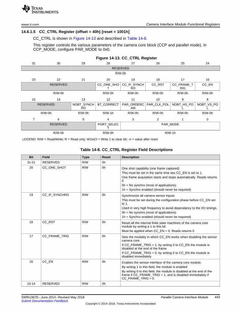
www.ti.com Camera Interface Module Functional Registers
443SWRU367D–June 2014–Revised May 2018Submit Documentation Feedback
Copyright © 2014–2018, Texas Instruments Incorporated
Parallel Camera Interface Module
14.6.1.5 CC_CTRL Register (offset = 40h) [reset = 1001h]CC_CTRL is shown in Figure 14-13 and described in Table 14-8.
This register controls the various parameters of the camera core block (CCP and parallel mode). InCCP_MODE, configure PAR_MODE to 0x0.
Figure 14-13. CC_CTRL Register31 30 29 28 27 26 25 24
RESERVEDR/W-0h
23 22 21 20 19 18 17 16RESERVED CC_ONE_SHO
TCC_IF_SYNCH
ROCC_RST CC_FRAME_T
RIGCC_EN
R/W-0h R/W-0h R/W-0h R/W-0h R/W-0h R/W-0h
15 14 13 12 11 10 9 8RESERVED NOBT_SYNCH
ROBT_CORRECT PAR_ORDERC
AMPAR_CLK_POL NOBT_HS_PO
LNOBT_VS_PO
LR/W-0h R/W-0h R/W-1h R/W-0h R/W-0h R/W-0h R/W-0h
7 6 5 4 3 2 1 0RESERVED PORT_SELEC
TPAR_MODE
R/W-0h R/W-0h R/W-1h
LEGEND: R/W = Read/Write; R = Read only; W1toCl = Write 1 to clear bit; -n = value after reset
Table 14-8. CC_CTRL Register Field Descriptions
Bit Field Type Reset Description31-21 RESERVED R/W 0h
20 CC_ONE_SHOT R/W 0h One shot capability (one frame captured)This must be set in the same time ass CC_EN is set to 1.One frame acquisition starts and stops automatically. Reads returns00h = No synchro (most of applications)1h = Synchro enabled (should never be required)
19 CC_IF_SYNCHRO R/W 0h Synchronize all camera sensor inputsThis must be set during the configuration phase before CC_EN setto 1.Used in very high frequency to avoid dependancy to the I/O timings.0h = No synchro (most of applications)1h = Synchro enabled (should never be required)
18 CC_RST R/W 0h Reset all the internal finite state machines of the camera coremodule by writing a 1 to this bit.Must be applied when CC_EN = 0. Reads returns 0
17 CC_FRAME_TRIG R/W 0h Sets the modality in which CC_EN works when disabling the sensorcamera core.If CC_FRAME_TRIG = 1, by writing 0 to CC_EN the module isdisabled at the end of the frameIf CC_FRAME_TRIG = 0, by writing 0 to CC_EN the module isdisabled immediately
16 CC_EN R/W 0h Enables the sensor interface of the camera core module.By writing 1 to this field, the module is enabledBy writing 0 to this field, the module is disabled at the end of theframe if CC_FRAME_TRIG = 1, and is disabled immediately ifCC_FRAME_TRIG = 0.
15-14 RESERVED R/W 0h
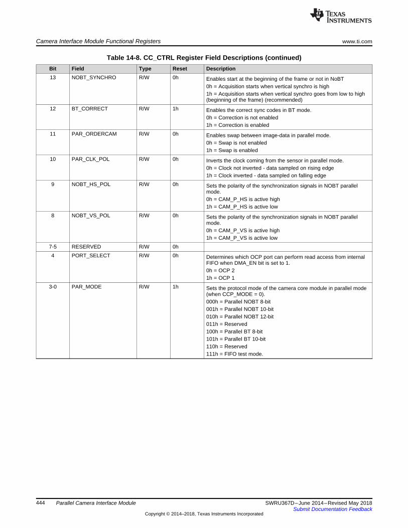
Camera Interface Module Functional Registers www.ti.com
444 SWRU367D–June 2014–Revised May 2018Submit Documentation Feedback
Copyright © 2014–2018, Texas Instruments Incorporated
Parallel Camera Interface Module
Table 14-8. CC_CTRL Register Field Descriptions (continued)Bit Field Type Reset Description13 NOBT_SYNCHRO R/W 0h Enables start at the beginning of the frame or not in NoBT
0h = Acquisition starts when vertical synchro is high1h = Acquisition starts when vertical synchro goes from low to high(beginning of the frame) (recommended)
12 BT_CORRECT R/W 1h Enables the correct sync codes in BT mode.0h = Correction is not enabled1h = Correction is enabled
11 PAR_ORDERCAM R/W 0h Enables swap between image-data in parallel mode.0h = Swap is not enabled1h = Swap is enabled
10 PAR_CLK_POL R/W 0h Inverts the clock coming from the sensor in parallel mode.0h = Clock not inverted - data sampled on rising edge1h = Clock inverted - data sampled on falling edge
9 NOBT_HS_POL R/W 0h Sets the polarity of the synchronization signals in NOBT parallelmode.0h = CAM_P_HS is active high1h = CAM_P_HS is active low
8 NOBT_VS_POL R/W 0h Sets the polarity of the synchronization signals in NOBT parallelmode.0h = CAM_P_VS is active high1h = CAM_P_VS is active low
7-5 RESERVED R/W 0h4 PORT_SELECT R/W 0h Determines which OCP port can perform read access from internal
FIFO when DMA_EN bit is set to 1.0h = OCP 21h = OCP 1
3-0 PAR_MODE R/W 1h Sets the protocol mode of the camera core module in parallel mode(when CCP_MODE = 0).000h = Parallel NOBT 8-bit001h = Parallel NOBT 10-bit010h = Parallel NOBT 12-bit011h = Reserved100h = Parallel BT 8-bit101h = Parallel BT 10-bit110h = Reserved111h = FIFO test mode.
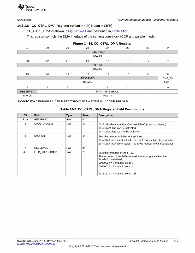
www.ti.com Camera Interface Module Functional Registers
445SWRU367D–June 2014–Revised May 2018Submit Documentation Feedback
Copyright © 2014–2018, Texas Instruments Incorporated
Parallel Camera Interface Module
14.6.1.6 CC_CTRL_DMA Register (offset = 44h) [reset = 16Fh]CC_CTRL_DMA is shown in Figure 14-14 and described in Table 14-9.
This register controls the DMA interface of the camera core block (CCP and parallel mode).
Figure 14-14. CC_CTRL_DMA Register31 30 29 28 27 26 25 24
RESERVEDR/W-0h
23 22 21 20 19 18 17 16RESERVED
R/W-0h
15 14 13 12 11 10 9 8RESERVED DMA_EN
R/W-0h R/W-1h
7 6 5 4 3 2 1 0RESERVED FIFO_THRESHOLD
R/W-0h R/W-7h
LEGEND: R/W = Read/Write; R = Read only; W1toCl = Write 1 to clear bit; -n = value after reset
Table 14-9. CC_CTRL_DMA Register Field Descriptions
Bit Field Type Reset Description31-9 RESERVED R/W 0h
8 DMA1_DISABLE R/W 1h DMA1 disable capability. Only use DMA0 (threshold-based).0h = DMA1 line can be activated1h = DMA1 line can not be activated
8 DMA_EN R/W 1h Sets the number of DMA request lines.0h = DMA interface disabled. The DMA request line stays inactive.1h = DMA interface enabled. The DMA request line is operational.
7 RESERVED R/W 0h6-0 FIFO_THRESHOLD R/W 7h Sets the threshold of the FIFO.
The assertion of the DMA request line takes place when thethreshold is reached.0000000h = Threshold set to 10000001h = Threshold set to 2...1111111h = Threshold set to 128

Camera Interface Module Functional Registers www.ti.com
446 SWRU367D–June 2014–Revised May 2018Submit Documentation Feedback
Copyright © 2014–2018, Texas Instruments Incorporated
Parallel Camera Interface Module
14.6.1.7 CC_CTRL_XCLK Register (offset = 48h) [reset = 0h]CC_CTRL_XCLK is shown in Figure 14-15 and described in Table 14-10.
This register controls the value of the clock divisor used to generate the external clock (parallel mode).Refer to Table 14-2 for details about the ratio of XCLK frequency.
Figure 14-15. CC_CTRL_XCLK Register31 30 29 28 27 26 25 24 23 22 21 20 19 18 17 16
RESERVEDR/W-0h
15 14 13 12 11 10 9 8 7 6 5 4 3 2 1 0RESERVED XCLK_DIV
R/W-0h R/W-0h
LEGEND: R/W = Read/Write; R = Read only; W1toCl = Write 1 to clear bit; -n = value after reset
Table 14-10. CC_CTRL_XCLK Register Field Descriptions
Bit Field Type Reset Description31-5 RESERVED R/W 0h4-0 XCLK_DIV R/W 0h Sets the clock divisor value for CAM_XCLK generation.
Based on CAM_MCLK (value of CAM_MCLK IS 96 MHz).Divider not enabled00000h = CAM_XCLK Stable low level00001h = CAM_XCLK Stable high levelfrom 2 to 30 = CAM_XCLK = CAM_MCLK / XCLK DIV11111h = Bypass - CAM_XCLK = CAM_MCLK
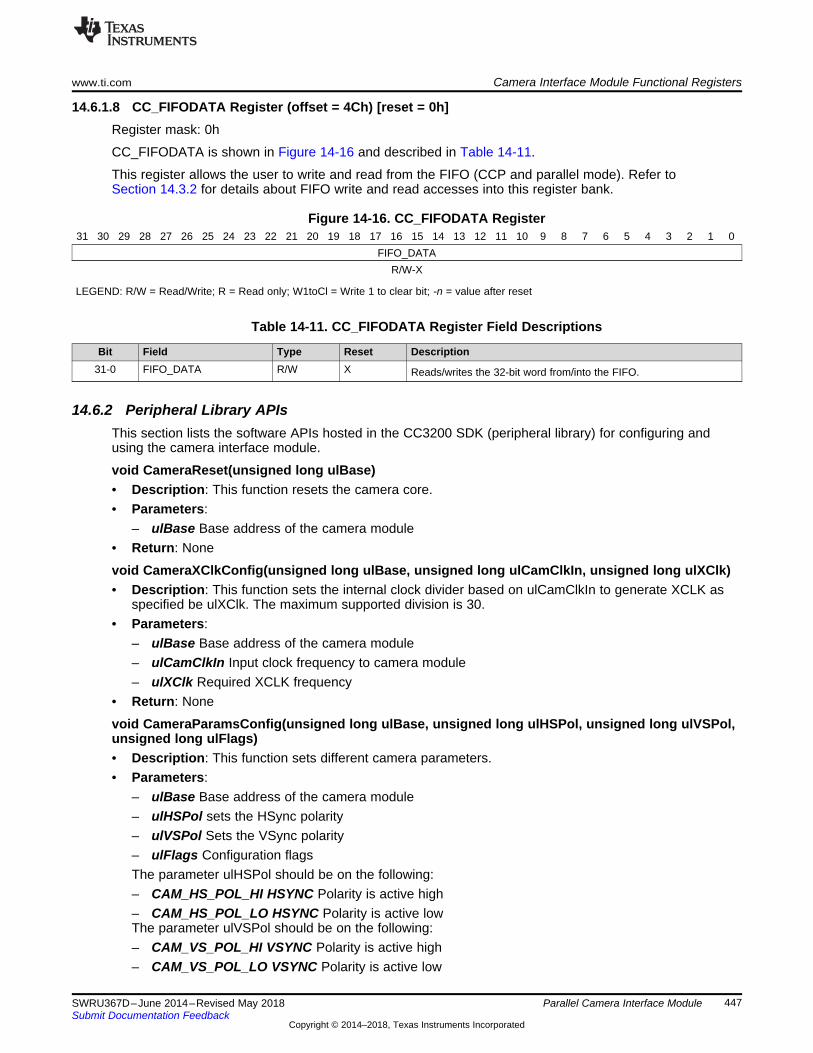
www.ti.com Camera Interface Module Functional Registers
447SWRU367D–June 2014–Revised May 2018Submit Documentation Feedback
Copyright © 2014–2018, Texas Instruments Incorporated
Parallel Camera Interface Module
14.6.1.8 CC_FIFODATA Register (offset = 4Ch) [reset = 0h]Register mask: 0h
CC_FIFODATA is shown in Figure 14-16 and described in Table 14-11.
This register allows the user to write and read from the FIFO (CCP and parallel mode). Refer toSection 14.3.2 for details about FIFO write and read accesses into this register bank.
Figure 14-16. CC_FIFODATA Register31 30 29 28 27 26 25 24 23 22 21 20 19 18 17 16 15 14 13 12 11 10 9 8 7 6 5 4 3 2 1 0
FIFO_DATAR/W-X
LEGEND: R/W = Read/Write; R = Read only; W1toCl = Write 1 to clear bit; -n = value after reset
Table 14-11. CC_FIFODATA Register Field Descriptions
Bit Field Type Reset Description31-0 FIFO_DATA R/W X Reads/writes the 32-bit word from/into the FIFO.
14.6.2 Peripheral Library APIsThis section lists the software APIs hosted in the CC3200 SDK (peripheral library) for configuring andusing the camera interface module.
void CameraReset(unsigned long ulBase)• Description: This function resets the camera core.• Parameters:
– ulBase Base address of the camera module• Return: None
void CameraXClkConfig(unsigned long ulBase, unsigned long ulCamClkIn, unsigned long ulXClk)• Description: This function sets the internal clock divider based on ulCamClkIn to generate XCLK as
specified be ulXClk. The maximum supported division is 30.• Parameters:
– ulBase Base address of the camera module– ulCamClkIn Input clock frequency to camera module– ulXClk Required XCLK frequency
• Return: None
void CameraParamsConfig(unsigned long ulBase, unsigned long ulHSPol, unsigned long ulVSPol,unsigned long ulFlags)• Description: This function sets different camera parameters.• Parameters:
– ulBase Base address of the camera module– ulHSPol sets the HSync polarity– ulVSPol Sets the VSync polarity– ulFlags Configuration flagsThe parameter ulHSPol should be on the following:– CAM_HS_POL_HI HSYNC Polarity is active high– CAM_HS_POL_LO HSYNC Polarity is active lowThe parameter ulVSPol should be on the following:– CAM_VS_POL_HI VSYNC Polarity is active high– CAM_VS_POL_LO VSYNC Polarity is active low
Camera Interface Module Functional Registers www.ti.com
448 SWRU367D–June 2014–Revised May 2018Submit Documentation Feedback
Copyright © 2014–2018, Texas Instruments Incorporated
Parallel Camera Interface Module
The parameter ulFlags can be logical OR of one or more of the following or 0:– CAM_PCLK_RISE_EDGE PCLK Polarity is active high– CAM_PCLK_FALL_EDGE PCLK Polarity is active low– CAM_ORDERCAM_SWAP Swap the byte order– CAM_NOBT_SYNCHRO Enable to start capture at start of frame– CAM_IF_SYNCHRO Synchronize all sensor inputs
• Return: None
void CameraXClkSet(unsigned long ulBase, unsigned char bXClkFlags)• Description: This function sets the internal divide in specified mode.• Parameters:
– ulBase Base address of the camera module– bXClkFlags Sets the divider modeThe parameter bXClkFlags should be one of the following:– CAM_XCLK_STABLE_LO XCLK line will be pulled low– CAM_XCLK_STABLE_HI XCLK line will be pulled high– CAM_XCLK_DIV_BYPASS XCLK divider is in bypass mode
• Return: None
void CameraDMAEnable(unsigned long ulBase)• Description: This function enables a transfer request to DMA from the camera. DMA-specific
configuration must be done separately.• Parameters:
– ulBase Base address of the camera module.• Return: None
void CameraDMADisable(unsigned long ulBase)• Description: This function masks a transfer request to DMA from the camera.• Parameters:
– ulBase Base address of the camera module.• Return: None
void CameraThresholdSet(unsigned long ulBase, unsigned long ulThreshold)• Description: This function sets the FIFO threshold for a DMA transfer request.• Parameters:
– ulBase Base address of the camera module– ulThreshold Specifies the FIFO level at which a DMA request is generated. This can be in the
range of 1 to 64.• Return: None
void CameraIntRegister(unsigned long ulBase, void (*pfnHandler)(void))• Description: This function registers and enables a global camera interrupt from the interrupt controller.
Individual camera interrupts source should be enabled using CameraIntEnable().• Parameters:
– ulBase Base address of the camera module• Return: None
void CameraIntUnregister(unsigned long ulBase)• Description: This function unregisters and disables the global camera interrupt from the interrupt
controller.• Parameters:
www.ti.com Camera Interface Module Functional Registers
449SWRU367D–June 2014–Revised May 2018Submit Documentation Feedback
Copyright © 2014–2018, Texas Instruments Incorporated
Parallel Camera Interface Module
– ulBase Base address of the camera module• Return: None.
void CameraIntEnable(unsigned long ulBase, unsigned long ulIntFlags)• Description: This function enables individual camera interrupt sources.• Parameters:
– ulBase Base address of the camera module– ulIntFlags Bit mask of the interrupt sources to be enabledThe parameter ulIntFlags should be logical OR of one or more of the following:– CAM_INT_DMA DMA done interrupt– CAM_INT_FE Frame end interrupt– CAM_INT_FSC_ERR Frame sync error interrupt– CAM_INT_FIFO_NOEMPTY FIFO empty interrupt– CAM_INT_FIFO_FULL FIFO full interrupt– CAM_INT_FIFO_THR FIFO reached threshold interrupt– CAM_INT_FIFO_OF FIFO overflow interrupt– CAN_INT_FIFO_UR FIFO underflow interrupt
• Return: None
void CameraIntDisable(unsigned long ulBase, unsigned long ulIntFlags)• Description: This function disables individual camera interrupt sources.• Parameters:
– ulBase Base address of the camera module– ulIntFlags Bit mask of the interrupt sources to be disabled
• Return: None
unsigned long CameraIntStatus(unsigned long ulBase)• Description: This functions returns the current interrupt status for the camera.• Parameters:
– ulBase Base address of the camera module• Return: Returns the current interrupt status, enumerated as a bit field of values described in
CameraIntEnable().
void CameraIntClear(unsigned long ulBase, unsigned long ulIntFlags)• Description: This function clears individual camera interrupt sources.• Parameters:
– ulBase Base address of the camera module– ulIntFlags Bit mask of the interrupt sources to be cleared
• Return: None
void CameraCaptureStart(unsigned long ulBase)• Description: This function starts the image capture over the configured camera interface. This function
should be called after completely configuring the camera module.• Parameters:
– ulBase Base address of the camera module• Return: None
void CameraCaptureStop(unsigned long ulBase, tBoolean bImmediate)• Description: This function stops the image capture over the camera interface. The capture is stopped
either immediately or at the end of the current frame, based on the bImmediate parameter.• Parameters:

Developer’s Guide www.ti.com
450 SWRU367D–June 2014–Revised May 2018Submit Documentation Feedback
Copyright © 2014–2018, Texas Instruments Incorporated
Parallel Camera Interface Module
– ulBase Base address of the camera module– bImmediate True to stop capture immediately, False to stop at the end of the frame
• Return: None
void CameraBufferRead(unsigned long ulBase,unsigned long *pBuffer, unsigned char ucSize)• Description: This function reads the camera buffer (FIFO).• Parameters:
– ulBase Base address of the camera module– pBuffer Pointer to the read buffer– ucSize Size to data to be read
• Return: None
14.7 Developer’s Guide
14.7.1 Using Peripheral Driver APIs for Capturing an Image1. The clock for camera peripheral must be configured and enabled. Peripherals are clock-gated by
default, and generate a bus fault if accessed without enabling the clock. The peripheral is ready to useafter the software reset:MAP_PRCMPeripheralClkEnable(PRCM_CAMERA, PRCM_RUN_MODE_CLK);MAP_PRCMPeripheralReset(PRCM_CAMERA);
2. The camera parameters must be set next, using the peripheral driver API CameraParamsConfig. Thisfunction sets the appropriate bits in the CAMERA_O_CC_CTRL register for controlling the variousparameters of the camera control block. The parameters are:• ulHSPol: Sets the polarity of the horizontal synchronization signal (CAM_P_HS). It can be either
CAM_HS_POL_HI or CAM_HS_POL_LO.• ulHSPol: Sets the polarity of the vertical synchronization signal (CAM_P_VS). It can be either
CAM_VS_POL_HI or CAM_VS_POL_LO.• ulFlags:
– Should be set to (CAM_ORDERCAM_SWAP | CAM_NOBT_SYNCHRO) for startingacquisition/capture when CAM_P_VS goes from low to high with swapping the image data inFIFO. See Section 14.3.1 for more details.
– Should be set to CAM_NOBT_SYNCHRO for starting acquisition/capture when CAM_P_VSgoes from low to high without swapping the image data in FIFO.
For high frequency operations, set CAM_IF_SYNCHRO to avoid dependency on the I/O timings.3. The interrupt-handler must be registered, using the peripheral driver API CameraIntRegister. This
function registers and enables global camera interrupts from the interrupt controller.4. The external-clock must be derived by programming the clock-divider values. The peripheral driver API
CameraXClkConfig sets the appropriate bits in this register for setting the internal clock divider.5. MCLK is, by default, set to 120 MHz, and cannot be modified. Hence, an XCLK of:
• 5 MHz can be derived by calling:
CameraXClkConfig(CAMERA_BASE, 120000000, 5000000)
• 10 MHz can be derived by calling:
CameraXClkConfig(CAMERA_BASE, 120000000, 10000000)Note: The maximum supported division is 30; a 2-MHz XCLK cannot be derived using a 120-MHzMCLK.
6. The FIFO threshold must be set using the peripheral driver API CameraThresholdSet. This functionsets the threshold at which to generate a DMA request.CameraThresholdSet(CAMERA_BASE, 8);
7. For handling the image data that is not a multiple of a FIFO threshold, the frame-end interrupt must beregistered using the peripheral API CameraIntEnable. This generates an interrupt at the end of everyframe:
www.ti.com Developer’s Guide
451SWRU367D–June 2014–Revised May 2018Submit Documentation Feedback
Copyright © 2014–2018, Texas Instruments Incorporated
Parallel Camera Interface Module
CameraIntEnable(CAMERA_BASE, CAM_INT_FE)
8. The DMA interface of the camera control block must be enabled by using the peripheral driver APICameraDMAEnable.CameraDMAEnable(CAMERA_BASE)
9. The DMA interface of the camera control block must be configured next. As an example, configure theDMA in ping-pong mode:• First initialize the DMA interface using the peripheral driver API UDMAInit.• The ping-pong transfer can be set up using the peripheral driver API DMASetupTransfer. The code
below code shows how this API could be used:
DMASetupTransfer(UDMA_CH22_CAMERA, UDMA_MODE_PINGPONG, <total_dma_elements>>, UDMA_SIZE_32,UDMA_ARB_8, (void *)CAM_BUFFER_ADDR, UDMA_SRC_INC_32,(void *)<data_buffer>,UDMA_DST_INC_32);
<data_buffer>+=<total_dma_elements>;/* Setup the buffer for pong */DMASetupTransfer(UDMA_CH22_CAMERA|UDMA_ALT_SELECT,
UDMA_MODE_PINGPONG, <total_dma_elements>,UDMA_SIZE_32,UDMA_ARB_8, (void *)CAM_BUFFER_ADDR,
UDMA_SRC_INC_32, (void*)<data_buffer>,UDMA_DST_INC_32);<data_buffer> += <total_dma_elements>;/* Setup buffer fornext ping */
10. The interrupts must be cleared and unmasked, by setting BIT-8 of DMA_DONE_INT_ACK andDMA_DONE_INT_MASK_CLR, respectively.
11. The image can now be captured using the peripheral driver API CameraCaptureStart. This functionenables the sensor interface of the camera core module.• An interrupt is continuously generated until the capture is stopped, and the interrupt-handler
registered above handles the interrupts appropriately.• Because the DMA is configured for ping-pong transfer, the <data_buffer> must be adjusted for the
next ping-pong transaction.• Depending on the value set for <total_dma_elements>, a DMA-Done interrupt is generated every
time after <total_dma_elements> elements are copied to memory.Code snippet for handling the camera interrupts:
void <camera_interrupt_handler>() /* Stop capture on receiving a frame-end */if(CameraIntStatus(CAMERA_BASE) &CAM_INT_FE)
CameraIntClear(CAMERA_BASE, CAM_INT_FE);CameraCaptureStop(CAMERA_BASE, true);
/* Check if ‘CAM_THRESHHOLD_DMA_DONE’ is active */if(<write_register>(DMA_DONE_INT_STS_RAW) & (1<<8))
/* Clear the interrupt */
<write_register>(DMA_DONE_INT_ACK) |= 1 << 8; <total_dma_elements> += <total_dma_elements>* <32-bits>; /* For every iteration, set either the ping or pong transactions */
if(<check condition for even iterations>)
DMASetupTransfer(UDMA_CH22_CAMERA, UDMA_MODE_PINGPONG,<total_dma_elements>,UDMA_SIZE_32,
UDMA_ARB_8, (void *)CAM_BUFFER_ADDR,UDMA_SRC_INC_32,
(void *)<data_buffer>, UDMA_DST_INC_32);
else(<check condition for odd iterations>)
DMASetupTransfer(UDMA_CH22_CAMERA|UDMA_ALT_SELECT,UDMA_MODE_PINGPONG, <total_dma_elements>,
UDMA_SIZE_32, UDMA_ARB_8, (void *)CAM_BUFFER_ADDR,UDMA_SRC_INC_32, (void *)<data_buffer>,
UDMA_DST_INC_32);
Developer’s Guide www.ti.com
452 SWRU367D–June 2014–Revised May 2018Submit Documentation Feedback
Copyright © 2014–2018, Texas Instruments Incorporated
Parallel Camera Interface Module
/* Setup the buffer for the next ping/pong */<data_buffer> += <total_dma_elements>;if (<on an error>)
/* Disable DMA and mask ‘CAM_THRESHHOLD_DMA_DONE’ */UDMAStopTransfer(UDMA_CH22_CAMERA);<write_register>(0x44026090) |= 1 << 8;
12. The capture can be stopped using the peripheral driver API CameraCaptureStop. This functiondisables the sensor interface of the camera core module. The sensor interface can be disabledimmediately, or at the end of current frame.
13. For stopping the image capture after a frame, disable the sensor interface immediately after theCAM_INT_FE interrupt.
14.7.2 Using Peripheral Driver APIs for Communicating with Image SensorsMost image sensors provide a two-wire serial interface for external MCUs to control them. This sectionshows how to use the CC3200 I2C interface to communicate with these image sensors. The CC3200includes one I2C module operating with standard (100-Kbps) or fast (400-Kbps) transmission speeds.
First configure and enable the clock for I2C peripheral. Peripherals are clock-gated by default andgenerate a bus fault if accessed without enabling the clock. The peripheral should be ready to use afterthe software reset.MAP_PRCMPeripheralClkEnable(PRCM_I2CA0, PRCM_RUN_MODE_CLK);MAP_PRCMPeripheralReset(PRCM_I2CA0);
The I2C master block must be configured and enabled next in either standard or fast mode, using theperipheral driver API MAP_I2CMasterInitExpClk. The function internally computes the clock divider toachieve the fastest speed less than or equal to the desired speed.MAP_I2CMasterInitExpClk (I2C_BASE, SYS_CLK, true); /* SYS_CLK is set to 80MHz */
The commands to the image sensor can then be written, and responses read. Normally a standardcommunication consists of:• Generating a START condition• Setting a I2C slave address• Transferring data• Generating a STOP condition
The master sends the slave address followed by the START condition. A slave with an address thatmatches this address responds by returning an acknowledgment bit. Once the slave addressing isachieved, data transfer can proceed byte-by-byte.
Peripheral driver APIs for writing and reading to and from an I2C slave:
I2CMasterSlaveAddrSet• Description: Sets the address that the I2C master places on the bus.• Parameters:
– ui32Base is the base address of the I2C master module.– ui8SlaveAddr is an 7-bit slave address.– bReceive is the flag indicating the type of communication with the slave.
I2CMasterDataPut• Description: Transmits a byte from the I2C master.• Parameters:
– ui32Base is the base address of the I2C master module.– ui8Data is data to be transmitted from the I2C master.
www.ti.com Developer’s Guide
453SWRU367D–June 2014–Revised May 2018Submit Documentation Feedback
Copyright © 2014–2018, Texas Instruments Incorporated
Parallel Camera Interface Module
I2CMasterDataGet• Description: Receives a byte that has been sent to the I2C master.• Parameters:
– ui32Base is the base address of the I2C master module
I2CMasterIntClearEx• Description: Clears I2C master interrupt sources.• Parameters:
– ui32Base is the base address of the I2C master module.– ui32IntFlags is a bit mask of the interrupt sources to be cleared.
I2CMasterTimeoutSet• Description: Sets the master clock timeout value.• Parameters:
– ui32Base is the base address of the I2C master module.– ui32Value is the number of I2C clocks before the timeout is asserted.
I2CMasterControl• Description: Controls the state of the I2C master module.• Parameters:
– ui32Base is the base address of the I2C master module.– ui32Cmd is the command to be issued to the I2C master module.
I2CMasterIntStatusEx• Description: Gets the current I2C master interrupt status.• Parameters:
– ui32Base is the base address of the I2C master module.– bMasked is false if the raw interrupt status is requested, and true if the masked interrupt status is
requested.
454 SWRU367D–June 2014–Revised May 2018Submit Documentation Feedback
Copyright © 2014–2018, Texas Instruments Incorporated
Power, Reset and Clock Management
Chapter 15SWRU367D–June 2014–Revised May 2018
Power, Reset and Clock Management
Topic ........................................................................................................................... Page
15.2 Overview ......................................................................................................... 45515.3 Power Management Control Architecture ............................................................ 45915.4 PRCM APIs ...................................................................................................... 46215.5 Peripheral Macros............................................................................................. 46815.6 Power Management Framework ......................................................................... 46915.7 PRCM Registers ............................................................................................... 470
www.ti.com Overview
455SWRU367D–June 2014–Revised May 2018Submit Documentation Feedback
Copyright © 2014–2018, Texas Instruments Incorporated
Power, Reset and Clock Management
15.1 TrademarksAMBA, CoreSight are trademarks of ARM Limited.
15.2 OverviewThe CC3200 SoC incorporates a highly optimized on-chip power management unit capable of operatingdirectly from battery, without any external regulator.
The on-chip PMU includes a set of high-efficiency, fast transient response DC-DC converters, LDOs, andreference voltage generators. The on-chip PMU is connected to the input supply directly, and generatesthe internal voltages required by the different sections of the chip across power modes. The PMU is tightlysynchronized with the WLAN radio, and avoids interference during radio receive and transmit operations.
The chip supports two supply configurations, which provide flexibility to system designers. In oneconfiguration, the input supply voltage at chip pin supports a range of 2.1 V to 3.6 V for active operation.In the second configuration, the chip can be supplied a pre-regulated 1.85 V that meets the ripple, load-transient, and peak current requirements. Refer to the CC3200 data sheet (SWAS032) for electricaldetails.
15.2.1 VBAT Wide-Voltage ConnectionIn the wide-voltage battery connection, the device is powered directly by the battery or pre-regulated 3.3-Vsupply. All other voltages required to operate the device are generated internally by the DC-DCconverters. This is the most common usage for the device, as it supports wide-voltage operation from 2.1V to 3.6 V.
15.2.2 Pre-Regulated 1.85 VThe pre-regulated 1.85-V mode of operation applies an external regulated 1.85 V directly to the pins 10,25, 33, 36, 37, 39, 44, 48, and 54 of the device. The VBAT and the VIO are also connected to the 1.85-Vsupply. The ANA1 DC-DC and PA DC-DC converters are bypassed. This mode provides the lowest BOMcount version.
NOTE: The chip auto-detects which of the two configurations is being used based on the state of theDC-DC pins. The chip then enables the DC-DCs accordingly.
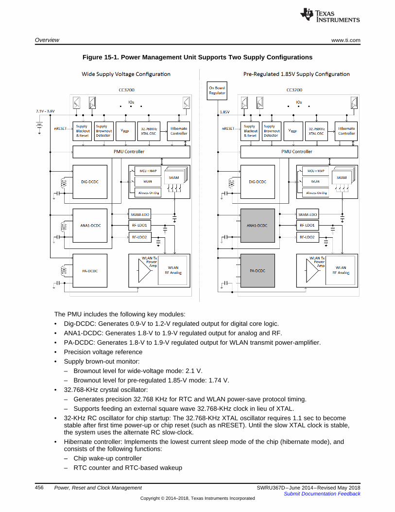
Overview www.ti.com
456 SWRU367D–June 2014–Revised May 2018Submit Documentation Feedback
Copyright © 2014–2018, Texas Instruments Incorporated
Power, Reset and Clock Management
Figure 15-1. Power Management Unit Supports Two Supply Configurations
The PMU includes the following key modules:• Dig-DCDC: Generates 0.9-V to 1.2-V regulated output for digital core logic.• ANA1-DCDC: Generates 1.8-V to 1.9-V regulated output for analog and RF.• PA-DCDC: Generates 1.8-V to 1.9-V regulated output for WLAN transmit power-amplifier.• Precision voltage reference• Supply brown-out monitor:
– Brownout level for wide-voltage mode: 2.1 V.– Brownout level for pre-regulated 1.85-V mode: 1.74 V.
• 32.768-KHz crystal oscillator:– Generates precision 32.768 KHz for RTC and WLAN power-save protocol timing.– Supports feeding an external square wave 32.768-KHz clock in lieu of XTAL.
• 32-KHz RC oscillator for chip startup: The 32.768-KHz XTAL oscillator requires 1.1 sec to becomestable after first time power-up or chip reset (such as nRESET). Until the slow XTAL clock is stable,the system uses the alternate RC slow-clock.
• Hibernate controller: Implements the lowest current sleep mode of the chip (hibernate mode), andconsists of the following functions:– Chip wake-up controller– RTC counter and RTC-based wakeup
www.ti.com Overview
457SWRU367D–June 2014–Revised May 2018Submit Documentation Feedback
Copyright © 2014–2018, Texas Instruments Incorporated
Power, Reset and Clock Management
– GPIO monitor and GPIO-based wakeup– 2×32-bit general purpose direct-battery powered retention register– Accessible from application processor through SoC-level interconnect– Manages the PMU and I/Os when core digital is powered off
• PMU controller:– Controls all the low-level real-time sequencing of the DC-DCs, LDOs, and references.– Implements the low-level sequences associated with sleep mode transitions– Not directly accessible from the application processor– PMU state transitions are initiated by control signals from the PRCM
Refer to the CC3200 data sheet (SWAS032) for the chip wake-up sequence and timing parameters.
15.2.3 Supply Brownout and BlackoutBROWNOUT is the state where the supply voltage falls below the chip brownout threshold. For widevoltage mode, Vbrownout = 2.1 V. For pre-regulated 1.85-V mode, Vbrownout = 1.74 V. All DC-DCs are disabledand all digital logic is power-gated, as long as the chip is in BROWNOUT state. The hibernate controller,2×32-bit general purpose retention register inside the hibernate controller, the 32.768-KHz XOSC, and theRTC counter are not impacted by BROWNOUT and continue to function. Once the supply voltage risesabove Vbrownout, the chip reboots.
BLACKOUT is the condition where the CC3x PMU incorporates a continuous time coarse analog supplyvoltage monitor that forces the PMU, including the hibernate controller, into a reset state where Vsupply <Vblackout. Vblackout is typically 1.4 V and varies with temperature.
BLACKOUT ensures that there is a deterministic reset of the control registers and flags inside thehibernate module just before the supply falls, to ensure that the system operations are terminated reliably.In this way, when a proper supply level is restored, the PMU starts from a clean reset state without anycorrupt control bits carried over from last session. The hibernate controller, 2×32-bit general purposeretention register inside the hibernate controller, the 32.768-KHz XOSC, and the RTC counter are all resetduring BLACKOUT. For a functional perspective, the effect of BLACKOUT is similar to that of pulling downthe chip reset pin (nRESET).
15.2.4 Application Processor Power ModesFrom the application processor (Cortex M4 and its peripherals) standpoint, the following power modes aresupported:• ACTIVE mode
– The processor is clocked at 80 MHz.– The required set of peripherals are running at configured clock rates.
• SLEEP mode– The processor is clock-gated until an interrupt event.– Reduces consumption by 3 mA with respect to ACTIVE.– Immediate wakeup.– The required set of peripherals is running at pre-configured clock rates.– By default, the sleep clock to the peripherals is disabled. If the application chooses to enter sleep
anytime and requires certain peripherals to be active, the sleep clock to the peripheral must beenabled in advance (see Section 15.7 and Section 15.4).
• DEEPSLEEP mode– The processor is clock-gated and PLL is disabled until an interrupt event.– Reduces consumption by 5 mA with respect to ACTIVE.– Using peripherals in conjunction with DEEPSLEEP is not recommended in the CC3200.
• Low-power deep-sleep mode (LPDS)– Up to 256 Kbyte of SRAM retention. No logic retention.
Overview www.ti.com
458 SWRU367D–June 2014–Revised May 2018Submit Documentation Feedback
Copyright © 2014–2018, Texas Instruments Incorporated
Power, Reset and Clock Management
• TI SW API and framework provided for transparent save and restore of processor context,peripheral, and pin configurations.
– Total system current (including Wi-Fi and network periodic wakeup) is as low as 700 uA.– When networking and Wi-Fi subsystems are disabled, the chip draws around 120 uA.
• 40-MHz XTAL and PLL are turned off. 32.768-KHz XTAL is kept alive.• Most digital logic is turned off. Digital supply voltage is reduced to 0.9 V.• SRAM can be retained in multiples of 64 KB.
– Processor and peripheral registers are not retained. Global always ON configurations at SoC levelare retained.
– Configurable wake-on-pad (one out of six pads).– Less that 5-mS wake-up latency.– Recommended for ultra-low power, always-connected cloud and Wi-Fi applications.
• Hibernate mode (HIB)– 32.768-KHz XTAL is kept alive .– Wake on RTC (for example, the 32-KHz slow clock counter) or selected GPIO.– No SRAM or logic retention.– 2×32-bit general purpose retention registers.
• These registers are powered by the input supply directly, and retain their content as long as thechip is not reset (nRESET=1) and the supply stays above the blackout level (1.4 V).
– Ultra-low current of 4 uA, including RTC.– Less than 10-mS wake-up latency.– Recommended for ultra-low power, infrequently-connected cloud and Wi-Fi applications.– A brief hibernation may also be used by software to implement a full system reboot as part of an
over-the-air software upgrade (OTA), or to restore the system to a guaranteed clean state followinga watchdog reset.
– Once a brownout condition is detected, the application software may choose to enter hibernatemode to prevent further oscillatory brownouts that may cause unpredictable system behavior andpossible damage to the end equipment. The system can subsequently be made to restart on a RTCtimer, on a chip reset, or on plugging of new batteries.
For CC3200 applications where battery life is critical, maximize the fraction of time spent in LPDS orhibernate modes compared to active and other sleep modes (SLEEP, DEEPSLEEP).
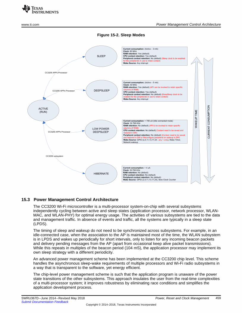
www.ti.com Power Management Control Architecture
459SWRU367D–June 2014–Revised May 2018Submit Documentation Feedback
Copyright © 2014–2018, Texas Instruments Incorporated
Power, Reset and Clock Management
Figure 15-2. Sleep Modes
15.3 Power Management Control ArchitectureThe CC3200 Wi-Fi microcontroller is a multi-processor system-on-chip with several subsystemsindependently cycling between active and sleep states (application processor, network processor, WLAN-MAC, and WLAN-PHY) for optimal energy usage. The activities of various subsystems are tied to the dataand management traffic. In absence of events and traffic, all the systems are typically in a sleep state(LPDS).
The timing of sleep and wakeup do not need to be synchronized across subsystems. For example, in anidle-connected case, when the association to the AP is maintained most of the time, the WLAN subsystemis in LPDS and wakes up periodically for short intervals, only to listen for any incoming beacon packetsand delivery pending messages from the AP (apart from occasional keep alive packet transmissions).While this repeats in multiples of the beacon period (104 mS), the application processor may implement itsown sleep strategy with a different periodicity.
An advanced power management scheme has been implemented at the CC3200 chip level. This schemehandles the asynchronous sleep-wake requirements of multiple processors and Wi-Fi radio subsystems ina way that is transparent to the software, yet energy efficient.
The chip-level power management scheme is such that the application program is unaware of the powerstate transitions of the other subsystems. This approach insulates the user from the real-time complexitiesof a multi-processor system; it improves robustness by eliminating race conditions and simplifies theapplication development process.
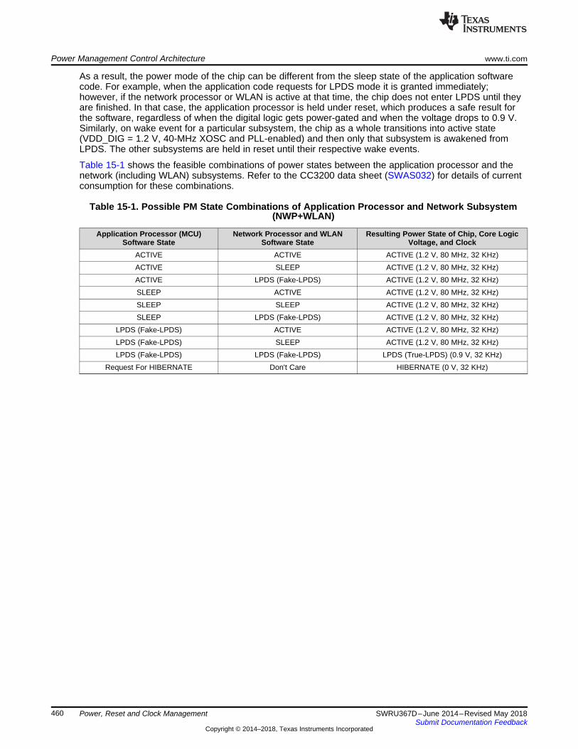
Power Management Control Architecture www.ti.com
460 SWRU367D–June 2014–Revised May 2018Submit Documentation Feedback
Copyright © 2014–2018, Texas Instruments Incorporated
Power, Reset and Clock Management
As a result, the power mode of the chip can be different from the sleep state of the application softwarecode. For example, when the application code requests for LPDS mode it is granted immediately;however, if the network processor or WLAN is active at that time, the chip does not enter LPDS until theyare finished. In that case, the application processor is held under reset, which produces a safe result forthe software, regardless of when the digital logic gets power-gated and when the voltage drops to 0.9 V.Similarly, on wake event for a particular subsystem, the chip as a whole transitions into active state(VDD_DIG = 1.2 V, 40-MHz XOSC and PLL-enabled) and then only that subsystem is awakened fromLPDS. The other subsystems are held in reset until their respective wake events.
Table 15-1 shows the feasible combinations of power states between the application processor and thenetwork (including WLAN) subsystems. Refer to the CC3200 data sheet (SWAS032) for details of currentconsumption for these combinations.
Table 15-1. Possible PM State Combinations of Application Processor and Network Subsystem(NWP+WLAN)
Application Processor (MCU)Software State
Network Processor and WLANSoftware State
Resulting Power State of Chip, Core LogicVoltage, and Clock
ACTIVE ACTIVE ACTIVE (1.2 V, 80 MHz, 32 KHz)ACTIVE SLEEP ACTIVE (1.2 V, 80 MHz, 32 KHz)ACTIVE LPDS (Fake-LPDS) ACTIVE (1.2 V, 80 MHz, 32 KHz)SLEEP ACTIVE ACTIVE (1.2 V, 80 MHz, 32 KHz)SLEEP SLEEP ACTIVE (1.2 V, 80 MHz, 32 KHz)SLEEP LPDS (Fake-LPDS) ACTIVE (1.2 V, 80 MHz, 32 KHz)
LPDS (Fake-LPDS) ACTIVE ACTIVE (1.2 V, 80 MHz, 32 KHz)LPDS (Fake-LPDS) SLEEP ACTIVE (1.2 V, 80 MHz, 32 KHz)LPDS (Fake-LPDS) LPDS (Fake-LPDS) LPDS (True-LPDS) (0.9 V, 32 KHz)
Request For HIBERNATE Don't Care HIBERNATE (0 V, 32 KHz)
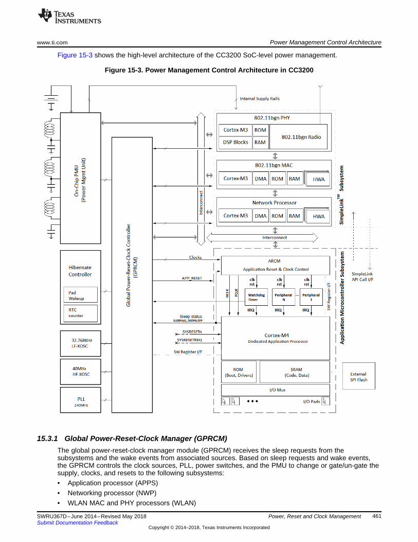
www.ti.com Power Management Control Architecture
461SWRU367D–June 2014–Revised May 2018Submit Documentation Feedback
Copyright © 2014–2018, Texas Instruments Incorporated
Power, Reset and Clock Management
Figure 15-3 shows the high-level architecture of the CC3200 SoC-level power management.
Figure 15-3. Power Management Control Architecture in CC3200
15.3.1 Global Power-Reset-Clock Manager (GPRCM)The global power-reset-clock manager module (GPRCM) receives the sleep requests from thesubsystems and the wake events from associated sources. Based on sleep requests and wake events,the GPRCM controls the clock sources, PLL, power switches, and the PMU to change or gate/un-gate thesupply, clocks, and resets to the following subsystems:• Application processor (APPS)• Networking processor (NWP)• WLAN MAC and PHY processors (WLAN)
Power Management Control Architecture www.ti.com
462 SWRU367D–June 2014–Revised May 2018Submit Documentation Feedback
Copyright © 2014–2018, Texas Instruments Incorporated
Power, Reset and Clock Management
Programmable system clock frequency (using PLL) is not supported in the CC3200, due to co-existencereasons. For ease of programming and system robustness, application code has limited access to the chippower and clock management infrastructure in CC3200. The software interface to power management islimited to a subset of GPRCM registers, which are accessed through a set of easy-to-use API functionsdescribed in Section 15.4.
15.3.2 Application Reset-Clock Manager (ARCM)The application processor subsystem uses a local reset and clock control module called ARCM. TheARCM controls the reset, clock muxing, and clock gating to the application-specific peripheral modules.ARCM has no power control functionality. The application processor subsystem is a single power domainmanaged by GPRCM at the SoC level. Power-gating at an individual peripheral level does not lead tosignificant savings in a high-performance multi-processor system, and is not supported in the CC3200.
The ARCM registers can be accessed either directly or through a set of easy-to-use API functionsdescribed in Section 15.4. The ARCM register map is described in Section 15.7.
15.4 PRCM APIsThis section gives an overview of the PRCM APIs provided in the CC3200 Software Development Kitperipheral library. For more details, refer to the SDK documentation.
15.4.1 MCU InitializationBooting from power-off or exiting hibernate low power mode, the user application can configure themandatory MCU parameters by calling void PRCMCC3200MCUInit() API.
void PRCMCC3200MCUInit(void)
Description: This function sets the mandatory configuration for the MCU.
Parameter: None
Return: None
15.4.2 Reset ControlMCU Reset (Software Reset)The MCU subsystem can be reset to its default state using the following API function call.
void PRCMMCUReset(tBoolean bIncludeSubsystem)
Description: This function performs a software reset of the MCU and associated peripherals. The coreresumes execution in the ROM bootloader, which reloads the user application from sFlash.
Parameter: bIncludeSubsystem – If true, the MCU and its associated peripherals are reset; if false, onlythe MCU is reset.
Return: None
15.4.3 Peripheral ResetIndividual peripherals can be reset to their default register state using the following API call.
void PRCMPeripheralReset(unsigned long ulPeripheral)
Description: This function performs a software reset of the specified peripheral.
Parameter: ulPeripheral – A valid peripheral macro (see Section 15.5)
Return: None
15.4.4 Reset CauseThe application processor restarts its execution from a reset vector after a reset. The application candetermine the cause of the reset using the following API.
www.ti.com PRCM APIs
463SWRU367D–June 2014–Revised May 2018Submit Documentation Feedback
Copyright © 2014–2018, Texas Instruments Incorporated
Power, Reset and Clock Management
unsigned long PRCMSysResetCauseGet(void)
Description: This function acquires the reason for an MCU reset. This is a sticky status.
Parameter: None
Return: Returns the MCU reset cause as one of the following:• PRCM_POWER_ON: Power-on reset• PRCM_LPDS_EXIT: Exiting from LPDS• PRCM_CORE_RESET: Software reset (core only)• PRCM_MCU_RESET: Software reset (core and associated peripherals)• PRCM_WDT_RESET: Watchdog reset• PRCM_SOC_RESET: Software SOC reset• PRCM_HIB_EXIT: Exiting from hibernate
15.4.5 Clock ControlIndividual peripherals can be kept clock-gated or un-gated across different power modes. Any access to aclock-gated peripheral results in a bus fault. The following APIs can control the peripheral clock gating.
void PRCMPeripheralClkEnable(unsigned long ulPeripheral, unsigned long ulClkFlags)
Description: This function un-gates the specified peripheral clock and makes the peripheral accessible.
Parameters:• ulPeripheral: One of the valid peripheral macros (see Section 15.5)• ulClkFlag: Power mode during which the clock is kept enabled and is bitwise or one or more of the
following:– PRCM_RUN_MODE_CLK: Un-gates clock to the peripheral during run mode.– PRCM_SLP_MODE_CLK: Keeps the clock un-gated during sleep.– PRCM_DSLP_MODE_CLK: Keeps the clock un-gated during deep sleep.
Return: None
void PRCMPeripheralClkDisable(unsigned long ulPeripheral, unsigned long ulClkFlags)
Description: This function gates a specified peripheral clock.
Parameter:• ulPeripheral: One of the valid peripheral macros (see Section 15.5).• ulClkFlag: Power mode during which the clock is kept disabled and is bitwise or one or more of the
following:– PRCM_RUN_MODE_CLK: Gates clock to the peripheral during run mode.– PRCM_SLP_MODE_CLK: Keeps the clock gated during sleep.– PRCM_DSLP_MODE_CLK: Keeps the clock gated during deep sleep.
Return: None
15.4.6 Low Power ModesSRAM Retention – The CC3200 SRAM is organized in 4 × 64-KB columns. By default, all SRAM columnsare configured to be retained across LPDS and deep sleep power modes. The application can enable ordisable retention per column by calling the following API with the appropriate parameters:
void PRCMSRAMRetentionEnable(unsigned long ulSramColSel, unsigned long ulFlags)
Description: This function reads from a specified OCR register.
Parameter:• ulSramColSel: Bit-packed representation of SRAM columns. ulSramColSel is logical or one or more
of the following:
PRCM APIs www.ti.com
464 SWRU367D–June 2014–Revised May 2018Submit Documentation Feedback
Copyright © 2014–2018, Texas Instruments Incorporated
Power, Reset and Clock Management
– PRCM_SRAM_COL_1: SRAM column 1– PRCM_SRAM_COL_2: SRAM column 2– PRCM_SRAM_COL_3: SRAM column 3– PRCM_SRAM_COL_4: SRAM column 4
• ulFlags: Bit-packed representation of power modes. ulFlags is logical or one or more of the following:– PRCM_SRAM_DSLP_RET: Configuration for DSLP– PRCM_SRAM_LPDS_RET: Configuration for LPDS
Return: None
void PRCMSRAMRetentionDisable(unsigned long ulSramColSel, unsigned long ulFlags)
Description: This function reads from a specified OCR register.
Parameter:• ulSramColSel: Bit-packed representation of SRAM columns. ulSramColSel is logical or one or more
of the following:– PRCM_SRAM_COL_1: SRAM column 1– PRCM_SRAM_COL_2: SRAM column 2– PRCM_SRAM_COL_3: SRAM column 3– PRCM_SRAM_COL_4: SRAM column 4
• ulFlags: Bit-packed representation of power modes. ulFlags is logical or one or more of the following:– PRCM_SRAM_DSLP_RET: Configuration for DSLP– PRCM_SRAM_LPDS_RET: Configuration for LPDS
Return: None
15.4.7 Sleep (SLEEP)This mode can be entered by calling the following API. In this mode, the core is halted at the point ofinvocation on this API with selective peripheral clock gating. The core resumes execution from the samelocation when it receives an interrupt.
void PRCMSleepEnter()Description: Enter sleep power mode by invoking a WFI instruction.
Parameter: None
Return: None
15.4.8 Deep Sleep (DEEPSLEEP)In this mode, the core is halted at the point of invocation on this API, with selective peripheral clock gatingand SRAM retention. The core resumes execution from the same location when it receives an interrupt.This mode can be entered by calling the following API.
void PRCMDeepSleepEnter ()
Description: Enter deep-sleep power mode by executing a WFI instruction.
Parameter: None
Return: None
By default, the entire SRAM is retained during DSLP. The user can enable or disable SRAM retentionusing the APIs PRCMSRAMRetentionEnable() and PRCMSRAMRetentionDisable(). See Section 15.4.6for more details.
15.4.9 Low-Power Deep Sleep (LPDS)In this mode, the MCU core and its associated peripheral are reset with selective SRAM column retention.
www.ti.com PRCM APIs
465SWRU367D–June 2014–Revised May 2018Submit Documentation Feedback
Copyright © 2014–2018, Texas Instruments Incorporated
Power, Reset and Clock Management
By default, the entire SRAM is retained during DSLP. The user can enable or disable SRAM retentionusing the APIs PRCMSRAMRetentionEnable() and PRCMSRAMRetentionDisable(). See Section 15.4.6for more details.
Core resumes its execution either in the ROM bootloader or a pre-configured location in SRAM (if the usersets restore info before entering LPDS) upon wakeup, due to configured wake sources which includes thefollowing:• Host IRQ – An interrupt from NWP• LPDS Timer – Dedicated LPDS timer• LPDS wakeup GPIOs – Six selected GPIOs
LPDS restore info can be set using the following API:
void PRCMLPDSRestoreInfoSet(unsigned long ulStackPtr, unsigned long ulProgCntr)
Description: This function sets the PC and stack pointer info that will be restored by the bootloader onexit from LPDS.
Parameter:• ulStackPtr: Stack pointer restored on exit from LPDS.• ulProgCntr: Program counter restored on exit from LPDS.
Return: None
LPDS wakeup sources can be configured using following APIs:
void PRCMLPDSWakeupSourceEnable(unsigned long ulLpdsWakeupSrc)
Description: This function enables the specified LPDS wake-up sources.
Parameter: ulLpdsWakeupSrc: Bit-packed representation of valid wake-up sources. ulLpdsWakeupSrcis bitwise or one or more of the following:• PRCM_LPDS_HOST_IRQ: Interrupt from NWP• PRCM_LPDS_GPIO: LPDS wake-up GPIOs• PRCM_LPDS_TIMER: Dedicated LPDS timer
Return: None
void PRCMLPDSWakeupSourceDisable(unsigned long ulLpdsWakeupSrc)
Description: This function disables the specified LPDS wake-up sources.
Parameter: ulLpdsWakeupSrc: Bit-packed representation of valid wake-up sources. ulLpdsWakeupSrcis bitwise or one or more of the following:• PRCM_LPDS_HOST_IRQ: Interrupt from NWP• PRCM_LPDS_GPIO: LPDS wake-up GPIOs• PRCM_LPDS_TIMER: Dedicated LPDS timer
Return: None
void PRCMLPDSIntervalSet(unsigned long ulTicks)
Description: This function sets the LPDS wake-up timer interval. The 32-bit timer is clocked at 32.768KHz and triggers a wakeup on expiry. The timer is started only when the system enters LPDS
Parameter: ulTicks: Wake-up interval in 32.768-KHz ticks.
Return: None
unsigned long PRCMLPDSWakeupCauseGet(void)
Description: This function gets the LPDS wake-up cause.
Parameter: None
Return: Returns the LPDS wake-up cause enumerated as one of the following:• PRCM_LPDS_HOST_IRQ: Interrupt from NWP
PRCM APIs www.ti.com
466 SWRU367D–June 2014–Revised May 2018Submit Documentation Feedback
Copyright © 2014–2018, Texas Instruments Incorporated
Power, Reset and Clock Management
• PRCM_LPDS_GPIO: LPDS wake-up GPIOs• PRCM_LPDS_TIMER: Dedicated LPDS timer
void PRCMLPDSWakeUpGPIOSelect(unsigned long ulGPIOPin, unsigned long ulType)
Description: Sets the specified GPIO as the wake-up source, and configures that GPIO to sense-specified.
Parameter:• ulGPIOPin: One of the valid LPDS wake-up GPIOs. ulGPIOPin can be one of the following:
– PRCM_LPDS_GPIO2: GPIO 2– PRCM_LPDS_GPIO4: GPIO 4– PRCM_LPDS_GPIO13: GPIO 13– PRCM_LPDS_GPIO17: GPIO 17– PRCM_LPDS_GPIO11: GPIO 11– PRCM_LPDS_GPIO24: GPIO 24
• ulType: Event Type. ulType can be one of the following:– PRCM_LPDS_LOW_LEVEL: GPIO is held low (0)– PRCM_LPDS_HIGH_LEVEL: GPIO is held high (1)– PRCM_LPDS_FALL_EDGE: GPIO changes from high to low– PRCM_LPDS_RISE_EDGE: GPIO changes from low to high
Return: None
The user application can put the system in LPDS by invoking following the API function:
void PRCMLPDSEnter(void)
Description: This function puts the system into low-power deep-sleep (LPDS) power mode, and shouldbe invoked after configuring the wake source, SRAM retention configuration, and system restoreconfiguration.
Parameter: None
Return: None
15.4.10 Hibernate (HIB)In this mode, the entire SOC loses its state, including the MCU subsystem, the NWP subsystem, andSRAM except 2 × 32-bit OCR registers and the free-running slow-clock counter. Core resumes itsexecution in the ROM bootloader upon wakeup due to configured wake sources, which include thefollowing:• Slow clock counter – Always-on 32.768-KHz counter• HIB wakeup GPIOs – Six selected GPIOs
Hibernate wake-up sources are configured using following APIs:
void PRCMHibernateWakeupSourceEnable(unsigned long ulHIBWakupSrc)
Description: This function enables the specified HIB wake-up sources.
Parameter: ulHIBWakupSrc: Bit-packed representation of valid wake-up sources. ulHIBWakupSrc isbitwise or one or more of the following:• PRCM_HIB_SLOW_CLK_CTR: Slow clock counter• PRCM_HIB_GPIO2: GPIO 2• PRCM_HIB_GPIO4: GPIO 4• PRCM_HIB_GPIO13: GPIO 13• PRCM_HIB_GPIO17: GPIO 17• PRCM_HIB_GPIO11: GPIO 11
www.ti.com PRCM APIs
467SWRU367D–June 2014–Revised May 2018Submit Documentation Feedback
Copyright © 2014–2018, Texas Instruments Incorporated
Power, Reset and Clock Management
• PRCM_HIB_GPIO24: GPIO 24
Return: None
void PRCMHibernateWakeupSourceDisable(unsigned long ulHIBWakupSrc)
Description: This function disables the specified HIB wake-up sources.
Parameter: ulHIBWakupSrc: Bit-packed representation of valid wake-up sources. ulHIBWakupSrc isbitwise or one or more of the following:• PRCM_HIB_SLOW_CLK_CTR: Slow clock counter• PRCM_HIB_GPIO2: GPIO 2• PRCM_HIB_GPIO4: GPIO 4• PRCM_HIB_GPIO13: GPIO 13• PRCM_HIB_GPIO17: GPIO 17• PRCM_HIB_GPIO11: GPIO 11• PRCM_HIB_GPIO24: GPIO 24
Return: None
unsigned long PRCMHibernateWakeupCauseGet(void)
Description: This function gets the HIB wake-up cause.
Parameter: None
Return: Returns the HIB wake-up cause enumerated as one of the following:• PRCM_HIB_WAKEUP_CAUSE_SLOW_CLOCK: Slow clock counter• PRCM_HIB_WAKEUP_CAUSE_GPIO: HIB wake-up GPIOs
void PRCMHibernateWakeUpGPIOSelect(unsigned long ulMultiGPIOBitMap, unsigned long ulType)
Description: Sets the specified GPIOs as wake-up source and configures them to sense the specifiedevent.
Parameter:• ulMultiGPIOBitMap: One of the valid HIB wake-up GPIOs. ulMultiGPIOBitMap is logical OR of one or
more of the following:– PRCM_LPDS_GPIO2: GPIO 2– PRCM_LPDS_GPIO4: GPIO 4– PRCM_LPDS_GPIO13: GPIO 13– PRCM_LPDS_GPIO17: GPIO 17– PRCM_LPDS_GPIO11: GPIO 11– PRCM_LPDS_GPIO24: GPIO 24
• ulType: Event Type. ulType can be one of the following:– PRCM_HIB_LOW_LEVEL: GPIO is held low (0)– PRCM_HIB_HIGH_LEVEL: GPIO is held high (1)– PRCM_HIB_FALL_EDGE: GPIO changes from High to Low– PRCM_HIB_RISE_EDGE: GPIO changes from Low to High
Return: None
void PRCMHibernateIntervalSet(unsigned long long ullTicks)
Description: This function sets the HIB wake-up interval based on the current slow clock count. The 48-bit timer is clocked at 32.768 KHz and triggers a wakeup when the counter reaches a particular value. Thefunction computes the wake-up count value by adding a specified interval to the current value of the slowclock counter.
Parameter: ullTicks: Wake-up interval in 32.768-KHz ticks
PRCM APIs www.ti.com
468 SWRU367D–June 2014–Revised May 2018Submit Documentation Feedback
Copyright © 2014–2018, Texas Instruments Incorporated
Power, Reset and Clock Management
Return: None
The application can put the system in HIB by invoking the following API:
void PRCMHibernateEnter (void)
Description: This function puts the system into hibernate power mode.
Parameter: None
Return: None
Two 32-bit on-chip retention registers (OCR) retained during the hibernate power mode can be accessedusing the following APIs:
void PRCMOCRRegisterWrite(unsigned char ucIndex, unsigned long ulRegValue)
Description: This function writes into a specified OCR register.
Parameter:• ucIndex: Selects one out of two available registers, 0 or 1• ulRegValue: 32-bit value
Return: None
unsigned long PRCMOCRRegisterRead(unsigned char ucIndex)
Description: This function reads from a specified OCR register.
Parameter: ucIndex: Selects one out of two available registers, 0 or 1
Return: Returns a 32-bit value read from a specified OCR register.
15.4.11 Slow Clock CounterThe CC3200 has a 48-bit on-chip always-on slow counter running at 32.768 KHz, which can wake up thedevice from hibernate low-power mode, or generate an interrupt to the core on counting a particular matchvalue. The following API returns the current value of the counter:
unsigned long PRCMSlowClkCtrGet(void)
Description: This function reads from a specified OCR register.
Parameter: None
Return: None
To set the match value to receive an interrupt call, use the following API with the appropriate value:
void PRCMSlowClkCtrMatchSet(unsigned long long ullTicks)
Description: This function sets the match value of the slow clock triggered interrupt.
Parameter: ullTicks 48-bit match value
Return: None
15.5 Peripheral Macros
Table 15-2. Peripheral Macro Table
Macro DescriptionPRCM_CAMERA Camera interface
PRCM_I2S I2S interfacePRCM_SDHOST SDHost interface
PRCM_GSPI General purpose SPI interfacePRCM_UDMA uDMA module
PRCM_GPIOA0 General Purpose IO port A0
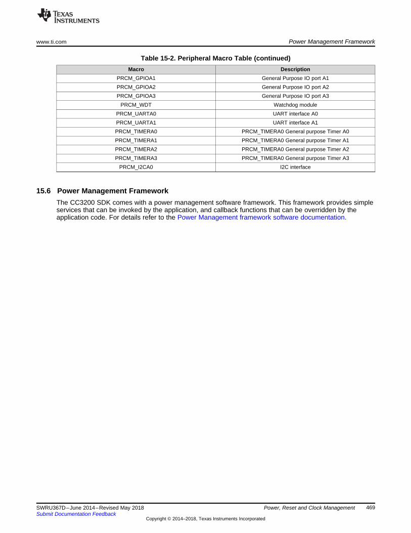
www.ti.com Power Management Framework
469SWRU367D–June 2014–Revised May 2018Submit Documentation Feedback
Copyright © 2014–2018, Texas Instruments Incorporated
Power, Reset and Clock Management
Table 15-2. Peripheral Macro Table (continued)Macro Description
PRCM_GPIOA1 General Purpose IO port A1PRCM_GPIOA2 General Purpose IO port A2PRCM_GPIOA3 General Purpose IO port A3
PRCM_WDT Watchdog modulePRCM_UARTA0 UART interface A0PRCM_UARTA1 UART interface A1PRCM_TIMERA0 PRCM_TIMERA0 General purpose Timer A0PRCM_TIMERA1 PRCM_TIMERA0 General purpose Timer A1PRCM_TIMERA2 PRCM_TIMERA0 General purpose Timer A2PRCM_TIMERA3 PRCM_TIMERA0 General purpose Timer A3
PRCM_I2CA0 I2C interface
15.6 Power Management FrameworkThe CC3200 SDK comes with a power management software framework. This framework provides simpleservices that can be invoked by the application, and callback functions that can be overridden by theapplication code. For details refer to the Power Management framework software documentation.
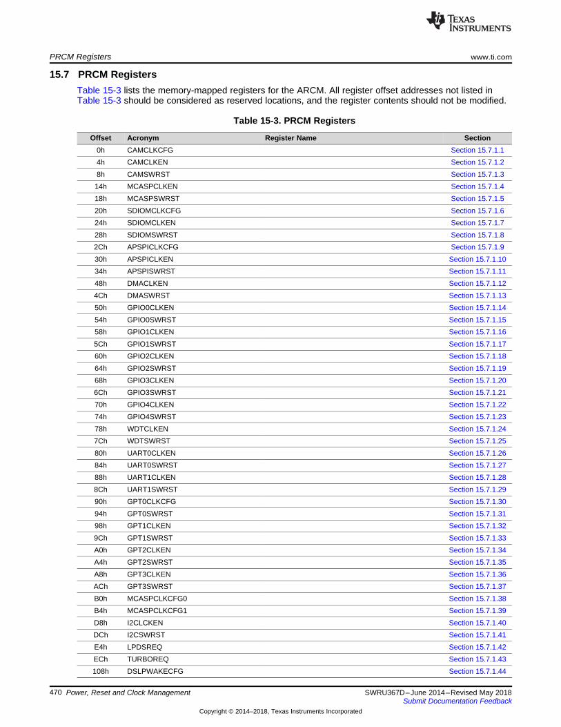
PRCM Registers www.ti.com
470 SWRU367D–June 2014–Revised May 2018Submit Documentation Feedback
Copyright © 2014–2018, Texas Instruments Incorporated
Power, Reset and Clock Management
15.7 PRCM RegistersTable 15-3 lists the memory-mapped registers for the ARCM. All register offset addresses not listed inTable 15-3 should be considered as reserved locations, and the register contents should not be modified.
Table 15-3. PRCM Registers
Offset Acronym Register Name Section0h CAMCLKCFG Section 15.7.1.14h CAMCLKEN Section 15.7.1.28h CAMSWRST Section 15.7.1.314h MCASPCLKEN Section 15.7.1.418h MCASPSWRST Section 15.7.1.520h SDIOMCLKCFG Section 15.7.1.624h SDIOMCLKEN Section 15.7.1.728h SDIOMSWRST Section 15.7.1.82Ch APSPICLKCFG Section 15.7.1.930h APSPICLKEN Section 15.7.1.1034h APSPISWRST Section 15.7.1.1148h DMACLKEN Section 15.7.1.124Ch DMASWRST Section 15.7.1.1350h GPIO0CLKEN Section 15.7.1.1454h GPIO0SWRST Section 15.7.1.1558h GPIO1CLKEN Section 15.7.1.165Ch GPIO1SWRST Section 15.7.1.1760h GPIO2CLKEN Section 15.7.1.1864h GPIO2SWRST Section 15.7.1.1968h GPIO3CLKEN Section 15.7.1.206Ch GPIO3SWRST Section 15.7.1.2170h GPIO4CLKEN Section 15.7.1.2274h GPIO4SWRST Section 15.7.1.2378h WDTCLKEN Section 15.7.1.247Ch WDTSWRST Section 15.7.1.2580h UART0CLKEN Section 15.7.1.2684h UART0SWRST Section 15.7.1.2788h UART1CLKEN Section 15.7.1.288Ch UART1SWRST Section 15.7.1.2990h GPT0CLKCFG Section 15.7.1.3094h GPT0SWRST Section 15.7.1.3198h GPT1CLKEN Section 15.7.1.329Ch GPT1SWRST Section 15.7.1.33A0h GPT2CLKEN Section 15.7.1.34A4h GPT2SWRST Section 15.7.1.35A8h GPT3CLKEN Section 15.7.1.36ACh GPT3SWRST Section 15.7.1.37B0h MCASPCLKCFG0 Section 15.7.1.38B4h MCASPCLKCFG1 Section 15.7.1.39D8h I2CLCKEN Section 15.7.1.40DCh I2CSWRST Section 15.7.1.41E4h LPDSREQ Section 15.7.1.42ECh TURBOREQ Section 15.7.1.43108h DSLPWAKECFG Section 15.7.1.44
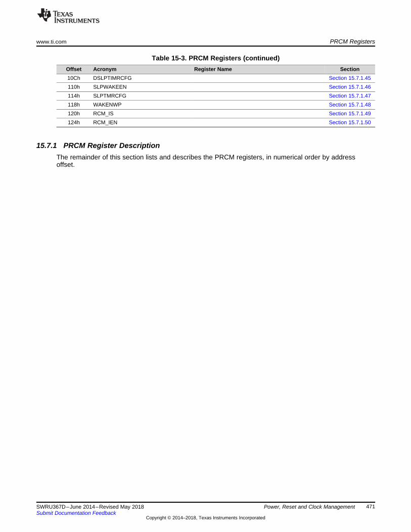
www.ti.com PRCM Registers
471SWRU367D–June 2014–Revised May 2018Submit Documentation Feedback
Copyright © 2014–2018, Texas Instruments Incorporated
Power, Reset and Clock Management
Table 15-3. PRCM Registers (continued)Offset Acronym Register Name Section10Ch DSLPTIMRCFG Section 15.7.1.45110h SLPWAKEEN Section 15.7.1.46114h SLPTMRCFG Section 15.7.1.47118h WAKENWP Section 15.7.1.48120h RCM_IS Section 15.7.1.49124h RCM_IEN Section 15.7.1.50
15.7.1 PRCM Register DescriptionThe remainder of this section lists and describes the PRCM registers, in numerical order by addressoffset.
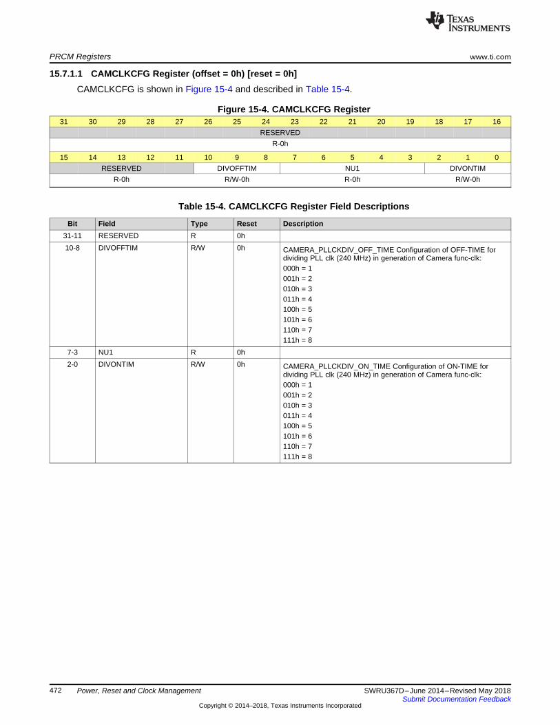
PRCM Registers www.ti.com
472 SWRU367D–June 2014–Revised May 2018Submit Documentation Feedback
Copyright © 2014–2018, Texas Instruments Incorporated
Power, Reset and Clock Management
15.7.1.1 CAMCLKCFG Register (offset = 0h) [reset = 0h]CAMCLKCFG is shown in Figure 15-4 and described in Table 15-4.
Figure 15-4. CAMCLKCFG Register31 30 29 28 27 26 25 24 23 22 21 20 19 18 17 16
RESERVEDR-0h
15 14 13 12 11 10 9 8 7 6 5 4 3 2 1 0RESERVED DIVOFFTIM NU1 DIVONTIM
R-0h R/W-0h R-0h R/W-0h
Table 15-4. CAMCLKCFG Register Field Descriptions
Bit Field Type Reset Description31-11 RESERVED R 0h10-8 DIVOFFTIM R/W 0h CAMERA_PLLCKDIV_OFF_TIME Configuration of OFF-TIME for
dividing PLL clk (240 MHz) in generation of Camera func-clk:000h = 1001h = 2010h = 3011h = 4100h = 5101h = 6110h = 7111h = 8
7-3 NU1 R 0h2-0 DIVONTIM R/W 0h CAMERA_PLLCKDIV_ON_TIME Configuration of ON-TIME for
dividing PLL clk (240 MHz) in generation of Camera func-clk:000h = 1001h = 2010h = 3011h = 4100h = 5101h = 6110h = 7111h = 8

www.ti.com PRCM Registers
473SWRU367D–June 2014–Revised May 2018Submit Documentation Feedback
Copyright © 2014–2018, Texas Instruments Incorporated
Power, Reset and Clock Management
15.7.1.2 CAMCLKEN Register (offset = 4h) [reset = 0h]CAMCLKEN is shown in Figure 15-5 and described in Table 15-5.
Figure 15-5. CAMCLKEN Register31 30 29 28 27 26 25 24
RESERVEDR-0h
23 22 21 20 19 18 17 16NU1 DSLPCLKENR-0h R-0h
15 14 13 12 11 10 9 8NU2 SLPCLKENR-0h R/W-0h
7 6 5 4 3 2 1 0NU3 RUNCLKENR-0h R/W-0h
Table 15-5. CAMCLKEN Register Field Descriptions
Bit Field Type Reset Description31-24 RESERVED R 0h23-17 NU1 R 0h
16 DSLPCLKEN R 0h CAMERA_DSLP_CLK_ENABLE0h = Disable camera clk during deep-sleep mode
15-9 NU2 R 0h8 SLPCLKEN R/W 0h CAMERA_SLP_CLK_ENABLE
0h = Disable camera clk during sleep mode1h = Enable camera clk during sleep mode
7-1 NU3 R 0h0 RUNCLKEN R/W 0h CAMERA_RUN_CLK_ENABLE
0h = Disable camera clk during run mode1h = Enable camera clk during run mode
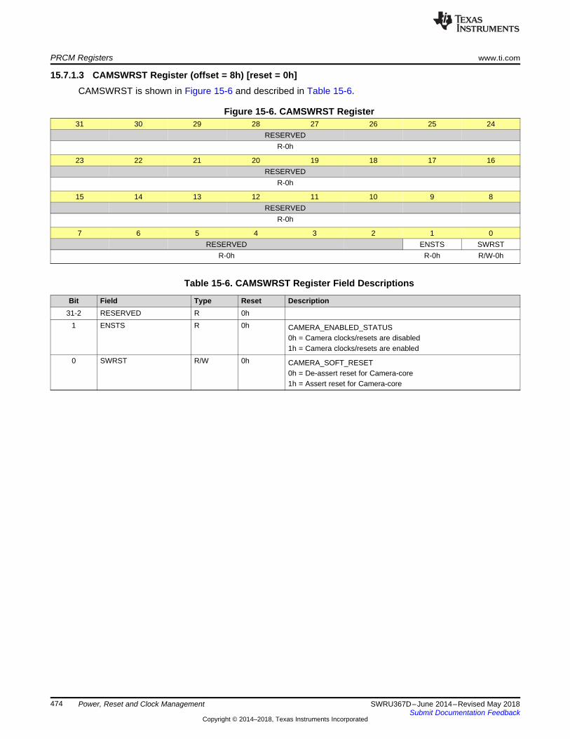
PRCM Registers www.ti.com
474 SWRU367D–June 2014–Revised May 2018Submit Documentation Feedback
Copyright © 2014–2018, Texas Instruments Incorporated
Power, Reset and Clock Management
15.7.1.3 CAMSWRST Register (offset = 8h) [reset = 0h]CAMSWRST is shown in Figure 15-6 and described in Table 15-6.
Figure 15-6. CAMSWRST Register31 30 29 28 27 26 25 24
RESERVEDR-0h
23 22 21 20 19 18 17 16RESERVED
R-0h
15 14 13 12 11 10 9 8RESERVED
R-0h
7 6 5 4 3 2 1 0RESERVED ENSTS SWRST
R-0h R-0h R/W-0h
Table 15-6. CAMSWRST Register Field Descriptions
Bit Field Type Reset Description31-2 RESERVED R 0h
1 ENSTS R 0h CAMERA_ENABLED_STATUS0h = Camera clocks/resets are disabled1h = Camera clocks/resets are enabled
0 SWRST R/W 0h CAMERA_SOFT_RESET0h = De-assert reset for Camera-core1h = Assert reset for Camera-core
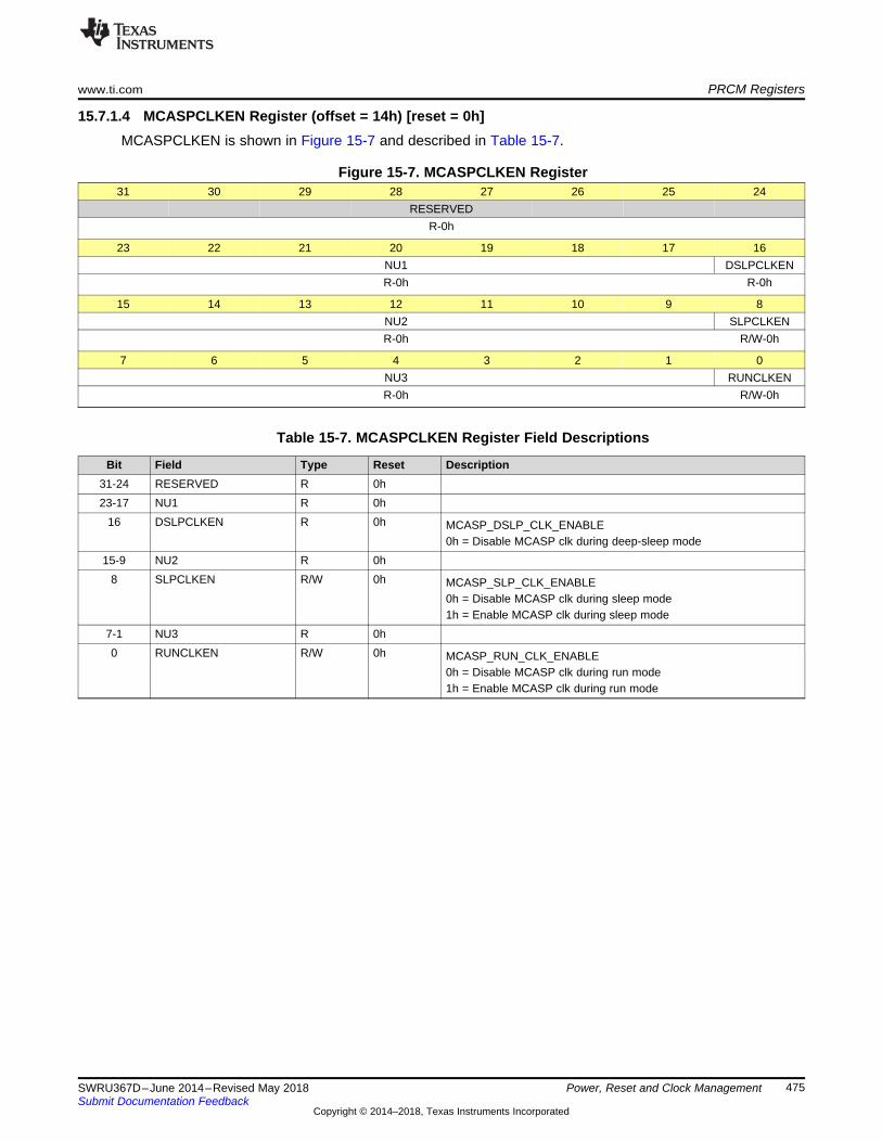
www.ti.com PRCM Registers
475SWRU367D–June 2014–Revised May 2018Submit Documentation Feedback
Copyright © 2014–2018, Texas Instruments Incorporated
Power, Reset and Clock Management
15.7.1.4 MCASPCLKEN Register (offset = 14h) [reset = 0h]MCASPCLKEN is shown in Figure 15-7 and described in Table 15-7.
Figure 15-7. MCASPCLKEN Register31 30 29 28 27 26 25 24
RESERVEDR-0h
23 22 21 20 19 18 17 16NU1 DSLPCLKENR-0h R-0h
15 14 13 12 11 10 9 8NU2 SLPCLKENR-0h R/W-0h
7 6 5 4 3 2 1 0NU3 RUNCLKENR-0h R/W-0h
Table 15-7. MCASPCLKEN Register Field Descriptions
Bit Field Type Reset Description31-24 RESERVED R 0h23-17 NU1 R 0h
16 DSLPCLKEN R 0h MCASP_DSLP_CLK_ENABLE0h = Disable MCASP clk during deep-sleep mode
15-9 NU2 R 0h8 SLPCLKEN R/W 0h MCASP_SLP_CLK_ENABLE
0h = Disable MCASP clk during sleep mode1h = Enable MCASP clk during sleep mode
7-1 NU3 R 0h0 RUNCLKEN R/W 0h MCASP_RUN_CLK_ENABLE
0h = Disable MCASP clk during run mode1h = Enable MCASP clk during run mode

PRCM Registers www.ti.com
476 SWRU367D–June 2014–Revised May 2018Submit Documentation Feedback
Copyright © 2014–2018, Texas Instruments Incorporated
Power, Reset and Clock Management
15.7.1.5 MCASPSWRST Register (offset = 18h) [reset = 0h]MCASPSWRST is shown in Figure 15-8 and described in Table 15-8.
Figure 15-8. MCASPSWRST Register31 30 29 28 27 26 25 24
RESERVEDR-0h
23 22 21 20 19 18 17 16RESERVED
R-0h
15 14 13 12 11 10 9 8RESERVED
R-0h
7 6 5 4 3 2 1 0RESERVED ENSTS SWRST
R-0h R-0h R/W-0h
Table 15-8. MCASPSWRST Register Field Descriptions
Bit Field Type Reset Description31-2 RESERVED R 0h
1 ENSTS R 0h MCASP_ENABLED_STATUS0h = MCASP Clocks/resets are disabled1h = MCASP Clocks/resets are enabled
0 SWRST R/W 0h MCASP_SOFT_RESET0h = De-assert reset for MCASP-core1h = Assert reset for MCASP-core

www.ti.com PRCM Registers
477SWRU367D–June 2014–Revised May 2018Submit Documentation Feedback
Copyright © 2014–2018, Texas Instruments Incorporated
Power, Reset and Clock Management
15.7.1.6 SDIOMCLKCFG Register (offset = 20h) [reset = 0h]SDIOMCLKCFG is shown in Figure 15-9 and described in Table 15-9.
Figure 15-9. SDIOMCLKCFG Register31 30 29 28 27 26 25 24 23 22 21 20 19 18 17 16
RESERVEDR-0h
15 14 13 12 11 10 9 8 7 6 5 4 3 2 1 0RESERVED DIVOFFTIM NU1 DIVONTIM
R-0h R/W-0h R-0h R/W-0h
Table 15-9. SDIOMCLKCFG Register Field Descriptions
Bit Field Type Reset Description31-11 RESERVED R 0h10-8 DIVOFFTIM R/W 0h MMCHS_PLLCKDIV_OFF_TIME Configuration of OFF-TIME for
dividing PLL clk (240 MHz) in generation of MMCHS func-clk:000h = 1001h = 2010h = 3011h = 4100h = 5101h = 6110h = 7111h = 8
7-3 NU1 R 0h2-0 DIVONTIM R/W 0h MMCHS_PLLCKDIV_ON_TIME Configuration of ON-TIME for
dividing PLL clk (240 MHz) in generation of MMCHS func-clk:000h = 1001h = 2010h = 3011h = 4100h = 5101h = 6110h = 7111h = 8
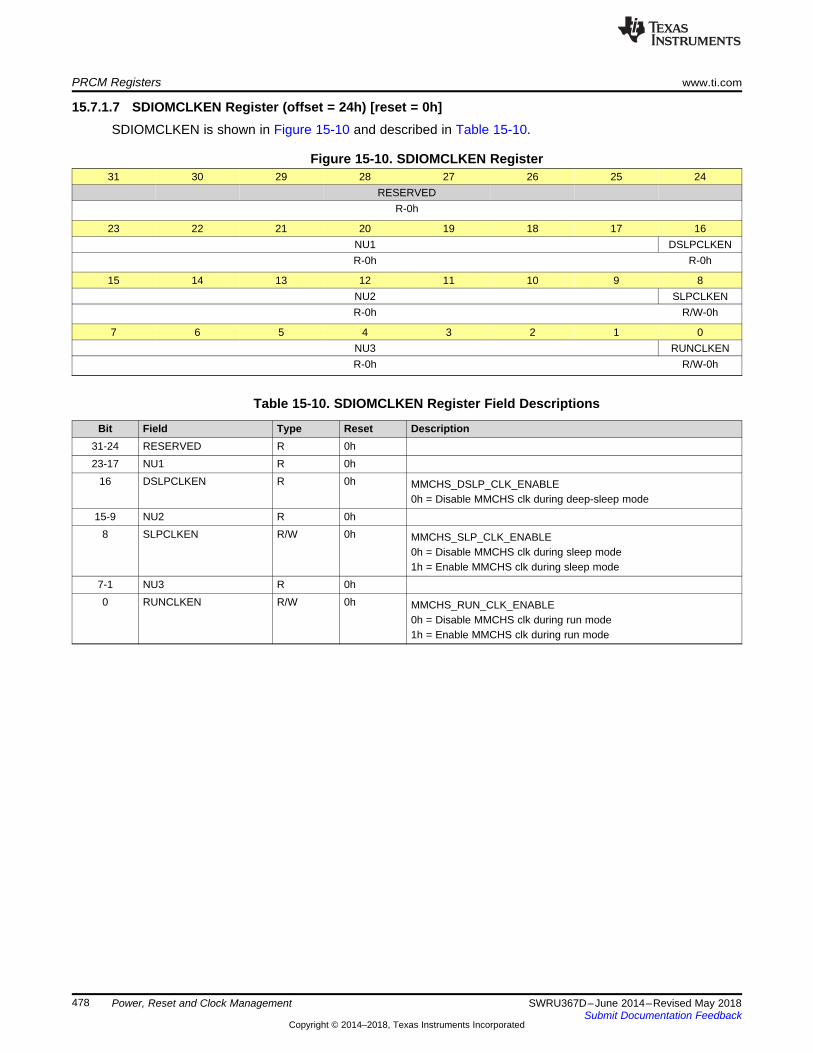
PRCM Registers www.ti.com
478 SWRU367D–June 2014–Revised May 2018Submit Documentation Feedback
Copyright © 2014–2018, Texas Instruments Incorporated
Power, Reset and Clock Management
15.7.1.7 SDIOMCLKEN Register (offset = 24h) [reset = 0h]SDIOMCLKEN is shown in Figure 15-10 and described in Table 15-10.
Figure 15-10. SDIOMCLKEN Register31 30 29 28 27 26 25 24
RESERVEDR-0h
23 22 21 20 19 18 17 16NU1 DSLPCLKENR-0h R-0h
15 14 13 12 11 10 9 8NU2 SLPCLKENR-0h R/W-0h
7 6 5 4 3 2 1 0NU3 RUNCLKENR-0h R/W-0h
Table 15-10. SDIOMCLKEN Register Field Descriptions
Bit Field Type Reset Description31-24 RESERVED R 0h23-17 NU1 R 0h
16 DSLPCLKEN R 0h MMCHS_DSLP_CLK_ENABLE0h = Disable MMCHS clk during deep-sleep mode
15-9 NU2 R 0h8 SLPCLKEN R/W 0h MMCHS_SLP_CLK_ENABLE
0h = Disable MMCHS clk during sleep mode1h = Enable MMCHS clk during sleep mode
7-1 NU3 R 0h0 RUNCLKEN R/W 0h MMCHS_RUN_CLK_ENABLE
0h = Disable MMCHS clk during run mode1h = Enable MMCHS clk during run mode
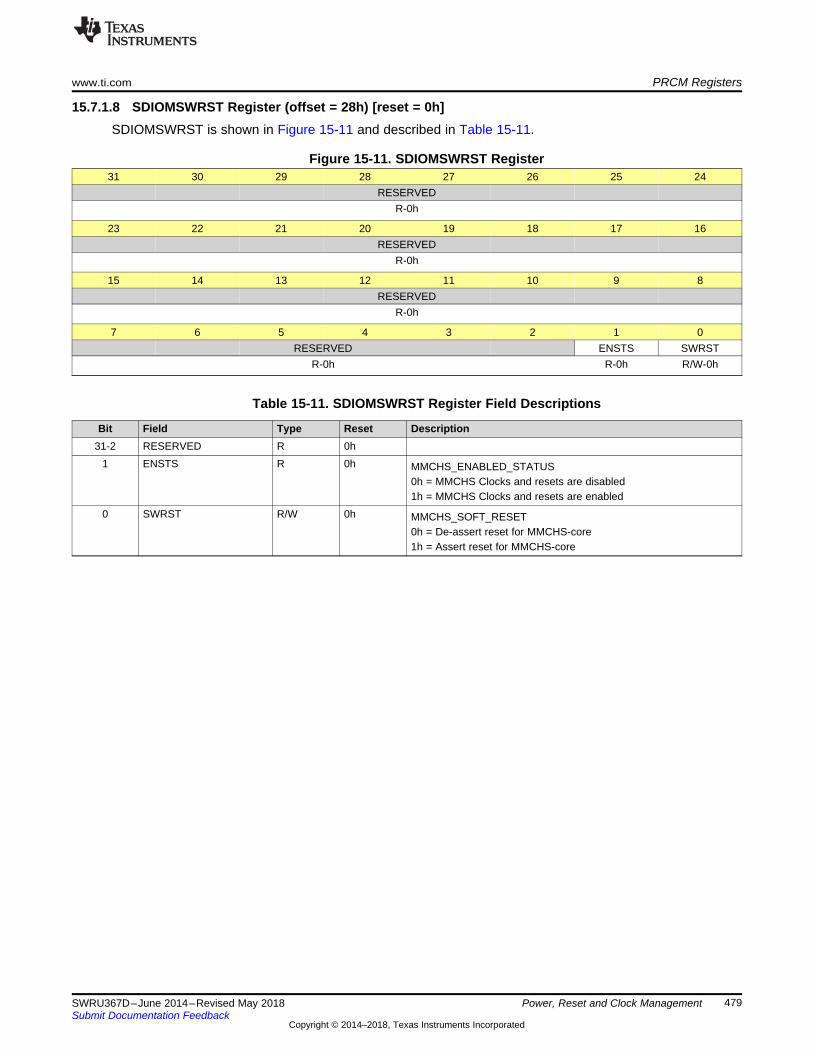
www.ti.com PRCM Registers
479SWRU367D–June 2014–Revised May 2018Submit Documentation Feedback
Copyright © 2014–2018, Texas Instruments Incorporated
Power, Reset and Clock Management
15.7.1.8 SDIOMSWRST Register (offset = 28h) [reset = 0h]SDIOMSWRST is shown in Figure 15-11 and described in Table 15-11.
Figure 15-11. SDIOMSWRST Register31 30 29 28 27 26 25 24
RESERVEDR-0h
23 22 21 20 19 18 17 16RESERVED
R-0h
15 14 13 12 11 10 9 8RESERVED
R-0h
7 6 5 4 3 2 1 0RESERVED ENSTS SWRST
R-0h R-0h R/W-0h
Table 15-11. SDIOMSWRST Register Field Descriptions
Bit Field Type Reset Description31-2 RESERVED R 0h
1 ENSTS R 0h MMCHS_ENABLED_STATUS0h = MMCHS Clocks and resets are disabled1h = MMCHS Clocks and resets are enabled
0 SWRST R/W 0h MMCHS_SOFT_RESET0h = De-assert reset for MMCHS-core1h = Assert reset for MMCHS-core
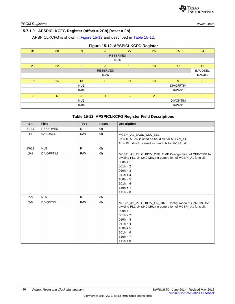
PRCM Registers www.ti.com
480 SWRU367D–June 2014–Revised May 2018Submit Documentation Feedback
Copyright © 2014–2018, Texas Instruments Incorporated
Power, Reset and Clock Management
15.7.1.9 APSPICLKCFG Register (offset = 2Ch) [reset = 0h]APSPICLKCFG is shown in Figure 15-12 and described in Table 15-12.
Figure 15-12. APSPICLKCFG Register31 30 29 28 27 26 25 24
RESERVEDR-0h
23 22 21 20 19 18 17 16RESERVED BAUDSEL
R-0h R/W-0h
15 14 13 12 11 10 9 8NU1 DIVOFFTIMR-0h R/W-0h
7 6 5 4 3 2 1 0NU2 DIVONTIMR-0h R/W-0h
Table 15-12. APSPICLKCFG Register Field Descriptions
Bit Field Type Reset Description31-17 RESERVED R 0h
16 BAUDSEL R/W 0h MCSPI_A1_BAUD_CLK_SEL0h = XTAL clk is used as baud clk for MCSPI_A11h = PLL divclk is used as baud clk for MCSPI_A1.
15-11 NU1 R 0h10-8 DIVOFFTIM R/W 0h MCSPI_A1_PLLCLKDIV_OFF_TIME Configuration of OFF-TIME for
dividing PLL clk (240 MHz) in generation of MCSPI_A1 func-clk:000h = 1001h = 2010h = 3011h = 4100h = 5101h = 6110h = 7111h = 8
7-3 NU2 R 0h2-0 DIVONTIM R/W 0h MCSPI_A1_PLLCLKDIV_ON_TIME Configuration of ON-TIME for
dividing PLL clk (240 MHz) in generation of MCSPI_A1 func-clk:000h = 1001h = 2010h = 3011h = 4100h = 5101h = 6110h = 7111h = 8

www.ti.com PRCM Registers
481SWRU367D–June 2014–Revised May 2018Submit Documentation Feedback
Copyright © 2014–2018, Texas Instruments Incorporated
Power, Reset and Clock Management
15.7.1.10 APSPICLKEN Register (offset = 30h) [reset = 0h]APSPICLKEN is shown in Figure 15-13 and described in Table 15-13.
Figure 15-13. APSPICLKEN Register31 30 29 28 27 26 25 24
RESERVEDR-0h
23 22 21 20 19 18 17 16NU1 DSLPCLKENR-0h R-0h
15 14 13 12 11 10 9 8NU2 SLPCLKENR-0h R/W-0h
7 6 5 4 3 2 1 0NU3 RUNCLKENR-0h R/W-0h
Table 15-13. APSPICLKEN Register Field Descriptions
Bit Field Type Reset Description31-24 RESERVED R 0h23-17 NU1 R 0h
16 DSLPCLKEN R 0h MCSPI_A1_DSLP_CLK_ENABLE0h = Disable MCSPI_A1 clk during deep-sleep mode
15-9 NU2 R 0h8 SLPCLKEN R/W 0h MCSPI_A1_SLP_CLK_ENABLE
0h = Disable MCSPI_A1 clk during sleep mode1h = Enable MCSPI_A1 clk during sleep mode
7-1 NU3 R 0h0 RUNCLKEN R/W 0h MCSPI_A1_RUN_CLK_ENABLE
0h = Disable MCSPI_A1 clk during run mode1h = Enable MCSPI_A1 clk during run mode
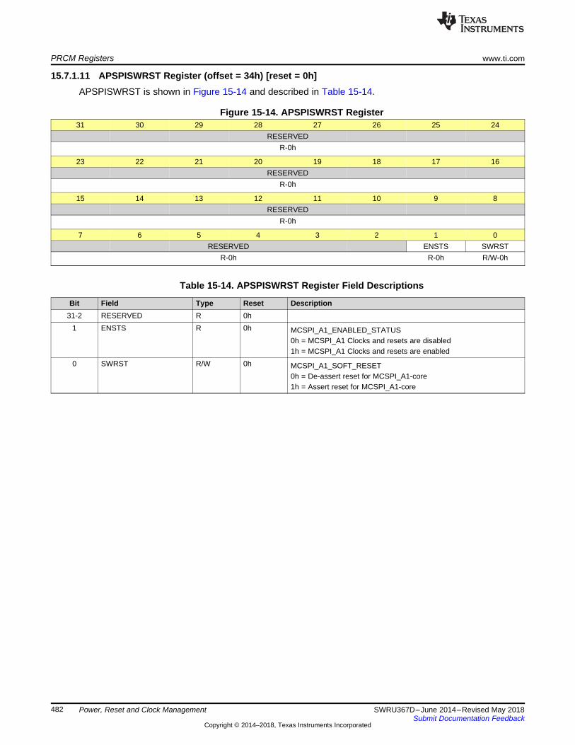
PRCM Registers www.ti.com
482 SWRU367D–June 2014–Revised May 2018Submit Documentation Feedback
Copyright © 2014–2018, Texas Instruments Incorporated
Power, Reset and Clock Management
15.7.1.11 APSPISWRST Register (offset = 34h) [reset = 0h]APSPISWRST is shown in Figure 15-14 and described in Table 15-14.
Figure 15-14. APSPISWRST Register31 30 29 28 27 26 25 24
RESERVEDR-0h
23 22 21 20 19 18 17 16RESERVED
R-0h
15 14 13 12 11 10 9 8RESERVED
R-0h
7 6 5 4 3 2 1 0RESERVED ENSTS SWRST
R-0h R-0h R/W-0h
Table 15-14. APSPISWRST Register Field Descriptions
Bit Field Type Reset Description31-2 RESERVED R 0h
1 ENSTS R 0h MCSPI_A1_ENABLED_STATUS0h = MCSPI_A1 Clocks and resets are disabled1h = MCSPI_A1 Clocks and resets are enabled
0 SWRST R/W 0h MCSPI_A1_SOFT_RESET0h = De-assert reset for MCSPI_A1-core1h = Assert reset for MCSPI_A1-core

www.ti.com PRCM Registers
483SWRU367D–June 2014–Revised May 2018Submit Documentation Feedback
Copyright © 2014–2018, Texas Instruments Incorporated
Power, Reset and Clock Management
15.7.1.12 DMACLKEN Register (offset = 48h) [reset = 0h]DMACLKEN is shown in Figure 15-15 and described in Table 15-15.
Figure 15-15. DMACLKEN Register31 30 29 28 27 26 25 24
RESERVEDR-0h
23 22 21 20 19 18 17 16RESERVED DSLPCLKEN
R-0h R/W-0h
15 14 13 12 11 10 9 8NU1 SLPCLKENR-0h R/W-0h
7 6 5 4 3 2 1 0NU2 RUNCLKENR-0h R/W-0h
Table 15-15. DMACLKEN Register Field Descriptions
Bit Field Type Reset Description31-17 RESERVED R 0h
16 DSLPCLKEN R/W 0h UDMA_A_DSLP_CLK_ENABLE0h = Disable UDMA_A clk during deep-sleep mode1h = Enable UDMA_A clk during deep-sleep mode
15-9 NU1 R 0h8 SLPCLKEN R/W 0h UDMA_A_SLP_CLK_ENABLE
0h = Disable UDMA_A clk during sleep mode1h = Enable UDMA_A clk during sleep mode
7-1 NU2 R 0h0 RUNCLKEN R/W 0h UDMA_A_RUN_CLK_ENABLE
0h = Disable UDMA_A clk during run mode1h = Enable UDMA_A clk during run mode
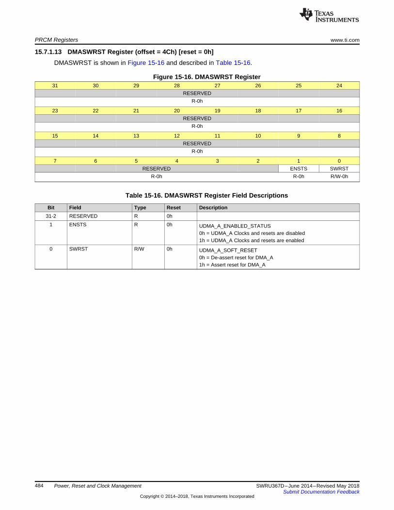
PRCM Registers www.ti.com
484 SWRU367D–June 2014–Revised May 2018Submit Documentation Feedback
Copyright © 2014–2018, Texas Instruments Incorporated
Power, Reset and Clock Management
15.7.1.13 DMASWRST Register (offset = 4Ch) [reset = 0h]DMASWRST is shown in Figure 15-16 and described in Table 15-16.
Figure 15-16. DMASWRST Register31 30 29 28 27 26 25 24
RESERVEDR-0h
23 22 21 20 19 18 17 16RESERVED
R-0h
15 14 13 12 11 10 9 8RESERVED
R-0h
7 6 5 4 3 2 1 0RESERVED ENSTS SWRST
R-0h R-0h R/W-0h
Table 15-16. DMASWRST Register Field Descriptions
Bit Field Type Reset Description31-2 RESERVED R 0h
1 ENSTS R 0h UDMA_A_ENABLED_STATUS0h = UDMA_A Clocks and resets are disabled1h = UDMA_A Clocks and resets are enabled
0 SWRST R/W 0h UDMA_A_SOFT_RESET0h = De-assert reset for DMA_A1h = Assert reset for DMA_A

www.ti.com PRCM Registers
485SWRU367D–June 2014–Revised May 2018Submit Documentation Feedback
Copyright © 2014–2018, Texas Instruments Incorporated
Power, Reset and Clock Management
15.7.1.14 GPIO0CLKEN Register (offset = 50h) [reset = 0h]GPIO0CLKEN is shown in Figure 15-17 and described in Table 15-17.
Figure 15-17. GPIO0CLKEN Register31 30 29 28 27 26 25 24
RESERVEDR-0h
23 22 21 20 19 18 17 16RESERVED DSLPCLKEN
R-0h R/W-0h
15 14 13 12 11 10 9 8NU1 SLPCLKENR-0h R/W-0h
7 6 5 4 3 2 1 0NU2 RUNCLKENR-0h R/W-0h
Table 15-17. GPIO0CLKEN Register Field Descriptions
Bit Field Type Reset Description31-17 RESERVED R 0h
16 DSLPCLKEN R/W 0h GPIO_A_DSLP_CLK_ENABLE0h = Disable GPIO_A clk during deep-sleep mode1h = Enable GPIO_A clk during deep-sleep mode
15-9 NU1 R 0h8 SLPCLKEN R/W 0h GPIO_A_SLP_CLK_ENABLE
0h = Disable GPIO_A clk during sleep mode1h = Enable GPIO_A clk during sleep mode
7-1 NU2 R 0h0 RUNCLKEN R/W 0h GPIO_A_RUN_CLK_ENABLE
0h = Disable GPIO_A clk during run mode1h = Enable GPIO_A clk during run mode

PRCM Registers www.ti.com
486 SWRU367D–June 2014–Revised May 2018Submit Documentation Feedback
Copyright © 2014–2018, Texas Instruments Incorporated
Power, Reset and Clock Management
15.7.1.15 GPIO0SWRST Register (offset = 54h) [reset = 0h]GPIO0SWRST is shown in Figure 15-18 and described in Table 15-18.
Figure 15-18. GPIO0SWRST Register31 30 29 28 27 26 25 24
RESERVEDR-0h
23 22 21 20 19 18 17 16RESERVED
R-0h
15 14 13 12 11 10 9 8RESERVED
R-0h
7 6 5 4 3 2 1 0RESERVED ENSTS SWRST
R-0h R-0h R/W-0h
Table 15-18. GPIO0SWRST Register Field Descriptions
Bit Field Type Reset Description31-2 RESERVED R 0h
1 ENSTS R 0h GPIO_A_ENABLED_STATUS0h = GPIO_A Clocks and resets are disabled1h = GPIO_A Clocks and resets are enabled
0 SWRST R/W 0h GPIO_A_SOFT_RESET0h = De-assert reset for GPIO_A1h = Assert reset for GPIO_A

www.ti.com PRCM Registers
487SWRU367D–June 2014–Revised May 2018Submit Documentation Feedback
Copyright © 2014–2018, Texas Instruments Incorporated
Power, Reset and Clock Management
15.7.1.16 GPIO1CLKEN Register (offset = 58h) [reset = 0h]GPIO1CLKEN is shown in Figure 15-19 and described in Table 15-19.
Figure 15-19. GPIO1CLKEN Register31 30 29 28 27 26 25 24
RESERVEDR-0h
23 22 21 20 19 18 17 16RESERVED DSLPCLKEN
R-0h R/W-0h
15 14 13 12 11 10 9 8NU1 SLPCLKENR-0h R/W-0h
7 6 5 4 3 2 1 0NU2 RUNCLKENR-0h R/W-0h
Table 15-19. GPIO1CLKEN Register Field Descriptions
Bit Field Type Reset Description31-17 RESERVED R 0h
16 DSLPCLKEN R/W 0h GPIO_B_DSLP_CLK_ENABLE0h = Disable GPIO_B clk during deep-sleep mode1h = Enable GPIO_B clk during deep-sleep mode
15-9 NU1 R 0h8 SLPCLKEN R/W 0h GPIO_B_SLP_CLK_ENABLE
0h = Disable GPIO_B clk during sleep mode1h = Enable GPIO_B clk during sleep mode
7-1 NU2 R 0h0 RUNCLKEN R/W 0h GPIO_B_RUN_CLK_ENABLE
0h = Disable GPIO_B clk during run mode1h = Enable GPIO_B clk during run mode

PRCM Registers www.ti.com
488 SWRU367D–June 2014–Revised May 2018Submit Documentation Feedback
Copyright © 2014–2018, Texas Instruments Incorporated
Power, Reset and Clock Management
15.7.1.17 GPIO1SWRST Register (offset = 5Ch) [reset = 0h]GPIO1SWRST is shown in Figure 15-20 and described in Table 15-20.
Figure 15-20. GPIO1SWRST Register31 30 29 28 27 26 25 24
RESERVEDR-0h
23 22 21 20 19 18 17 16RESERVED
R-0h
15 14 13 12 11 10 9 8RESERVED
R-0h
7 6 5 4 3 2 1 0RESERVED ENSTS SWRST
R-0h R-0h R/W-0h
Table 15-20. GPIO1SWRST Register Field Descriptions
Bit Field Type Reset Description31-2 RESERVED R 0h
1 ENSTS R 0h GPIO_B_ENABLED_STATUS0h = GPIO_B Clocks and resets are disabled1h = GPIO_B Clocks and resets are enabled
0 SWRST R/W 0h GPIO_B_SOFT_RESET0h = De-assert reset for GPIO_B1h = Assert reset for GPIO_B
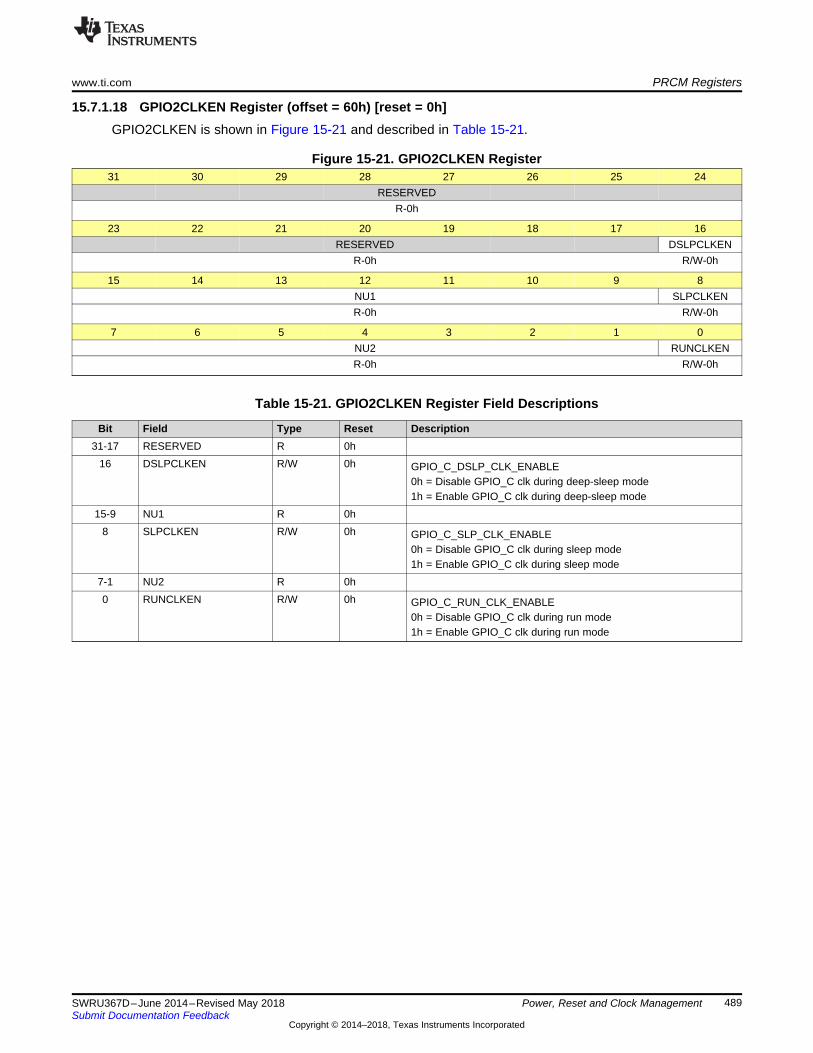
www.ti.com PRCM Registers
489SWRU367D–June 2014–Revised May 2018Submit Documentation Feedback
Copyright © 2014–2018, Texas Instruments Incorporated
Power, Reset and Clock Management
15.7.1.18 GPIO2CLKEN Register (offset = 60h) [reset = 0h]GPIO2CLKEN is shown in Figure 15-21 and described in Table 15-21.
Figure 15-21. GPIO2CLKEN Register31 30 29 28 27 26 25 24
RESERVEDR-0h
23 22 21 20 19 18 17 16RESERVED DSLPCLKEN
R-0h R/W-0h
15 14 13 12 11 10 9 8NU1 SLPCLKENR-0h R/W-0h
7 6 5 4 3 2 1 0NU2 RUNCLKENR-0h R/W-0h
Table 15-21. GPIO2CLKEN Register Field Descriptions
Bit Field Type Reset Description31-17 RESERVED R 0h
16 DSLPCLKEN R/W 0h GPIO_C_DSLP_CLK_ENABLE0h = Disable GPIO_C clk during deep-sleep mode1h = Enable GPIO_C clk during deep-sleep mode
15-9 NU1 R 0h8 SLPCLKEN R/W 0h GPIO_C_SLP_CLK_ENABLE
0h = Disable GPIO_C clk during sleep mode1h = Enable GPIO_C clk during sleep mode
7-1 NU2 R 0h0 RUNCLKEN R/W 0h GPIO_C_RUN_CLK_ENABLE
0h = Disable GPIO_C clk during run mode1h = Enable GPIO_C clk during run mode

PRCM Registers www.ti.com
490 SWRU367D–June 2014–Revised May 2018Submit Documentation Feedback
Copyright © 2014–2018, Texas Instruments Incorporated
Power, Reset and Clock Management
15.7.1.19 GPIO2SWRST Register (offset = 64h) [reset = 0h]GPIO2SWRST is shown in Figure 15-22 and described in Table 15-22.
Figure 15-22. GPIO2SWRST Register31 30 29 28 27 26 25 24
RESERVEDR-0h
23 22 21 20 19 18 17 16RESERVED
R-0h
15 14 13 12 11 10 9 8RESERVED
R-0h
7 6 5 4 3 2 1 0RESERVED ENSTS SWRST
R-0h R-0h R/W-0h
Table 15-22. GPIO2SWRST Register Field Descriptions
Bit Field Type Reset Description31-2 RESERVED R 0h
1 ENSTS R 0h GPIO_C_ENABLED_STATUS0h = GPIO_C Clocks and resets are disabled1h = GPIO_C Clocks and resets are enabled
0 SWRST R/W 0h GPIO_C_SOFT_RESET0h = De-assert reset for GPIO_C1h = Assert reset for GPIO_C

www.ti.com PRCM Registers
491SWRU367D–June 2014–Revised May 2018Submit Documentation Feedback
Copyright © 2014–2018, Texas Instruments Incorporated
Power, Reset and Clock Management
15.7.1.20 GPIO3CLKEN Register (offset = 68h) [reset = 0h]GPIO3CLKEN is shown in Figure 15-23 and described in Table 15-23.
Figure 15-23. GPIO3CLKEN Register31 30 29 28 27 26 25 24
RESERVEDR-0h
23 22 21 20 19 18 17 16RESERVED DSLPCLKEN
R-0h R/W-0h
15 14 13 12 11 10 9 8NU1 SLPCLKENR-0h R/W-0h
7 6 5 4 3 2 1 0NU2 RUNCLKENR-0h R/W-0h
Table 15-23. GPIO3CLKEN Register Field Descriptions
Bit Field Type Reset Description31-17 RESERVED R 0h
16 DSLPCLKEN R/W 0h GPIO_D_DSLP_CLK_ENABLE0h = Disable GPIO_D clk during deep-sleep mode1h = Enable GPIO_D clk during deep-sleep mode
15-9 NU1 R 0h8 SLPCLKEN R/W 0h GPIO_D_SLP_CLK_ENABLE
0h = Disable GPIO_D clk during sleep mode1h = Enable GPIO_D clk during sleep mode
7-1 NU2 R 0h0 RUNCLKEN R/W 0h GPIO_D_RUN_CLK_ENABLE
0h = Disable GPIO_D clk during run mode1h = Enable GPIO_D clk during run mode

PRCM Registers www.ti.com
492 SWRU367D–June 2014–Revised May 2018Submit Documentation Feedback
Copyright © 2014–2018, Texas Instruments Incorporated
Power, Reset and Clock Management
15.7.1.21 GPIO3SWRST Register (offset = 6Ch) [reset = 0h]GPIO3SWRST is shown in Figure 15-24 and described in Table 15-24.
Figure 15-24. GPIO3SWRST Register31 30 29 28 27 26 25 24
RESERVEDR-0h
23 22 21 20 19 18 17 16RESERVED
R-0h
15 14 13 12 11 10 9 8RESERVED
R-0h
7 6 5 4 3 2 1 0RESERVED ENSTS SWRST
R-0h R-0h R/W-0h
Table 15-24. GPIO3SWRST Register Field Descriptions
Bit Field Type Reset Description31-2 RESERVED R 0h
1 ENSTS R 0h GPIO_D_ENABLED_STATUS0h = GPIO_D Clocks and resets are disabled1h = GPIO_D Clocks and resets are enabled
0 SWRST R/W 0h GPIO_D_SOFT_RESET0h = De-assert reset for GPIO_D1h = Assert reset for GPIO_D

www.ti.com PRCM Registers
493SWRU367D–June 2014–Revised May 2018Submit Documentation Feedback
Copyright © 2014–2018, Texas Instruments Incorporated
Power, Reset and Clock Management
15.7.1.22 GPIO4CLKEN Register (offset = 70h) [reset = 0h]GPIO4CLKEN is shown in Figure 15-25 and described in Table 15-25.
Figure 15-25. GPIO4CLKEN Register31 30 29 28 27 26 25 24
RESERVEDR-0h
23 22 21 20 19 18 17 16RESERVED DSLPCLKEN
R-0h R/W-0h
15 14 13 12 11 10 9 8NU1 SLPCLKENR-0h R/W-0h
7 6 5 4 3 2 1 0NU2 RUNCLKENR-0h R/W-0h
Table 15-25. GPIO4CLKEN Register Field Descriptions
Bit Field Type Reset Description31-17 RESERVED R 0h
16 DSLPCLKEN R/W 0h GPIO_E_DSLP_CLK_ENABLE0h = Disable GPIO_E clk during deep-sleep mode1h = Enable GPIO_E clk during deep-sleep mode
15-9 NU1 R 0h8 SLPCLKEN R/W 0h GPIO_E_SLP_CLK_ENABLE
0h = Disable GPIO_E clk during sleep mode1h = Enable GPIO_E clk during sleep mode
7-1 NU2 R 0h0 RUNCLKEN R/W 0h GPIO_E_RUN_CLK_ENABLE
0h = Disable GPIO_E clk during run mode1h = Enable GPIO_E clk during run mode

PRCM Registers www.ti.com
494 SWRU367D–June 2014–Revised May 2018Submit Documentation Feedback
Copyright © 2014–2018, Texas Instruments Incorporated
Power, Reset and Clock Management
15.7.1.23 GPIO4SWRST Register (offset = 74h) [reset = 0h]GPIO4SWRST is shown in Figure 15-26 and described in Table 15-26.
Figure 15-26. GPIO4SWRST Register31 30 29 28 27 26 25 24
RESERVEDR-0h
23 22 21 20 19 18 17 16RESERVED
R-0h
15 14 13 12 11 10 9 8RESERVED
R-0h
7 6 5 4 3 2 1 0RESERVED ENSTS SWRST
R-0h R-0h R/W-0h
Table 15-26. GPIO4SWRST Register Field Descriptions
Bit Field Type Reset Description31-2 RESERVED R 0h
1 ENSTS R 0h GPIO_E_ENABLED_STATUS0h = GPIO_E Clocks and resets are disabled1h = GPIO_E Clocks and resets are enabled
0 SWRST R/W 0h GPIO_E_SOFT_RESET0h = De-assert reset for GPIO_E1h = Assert reset for GPIO_E
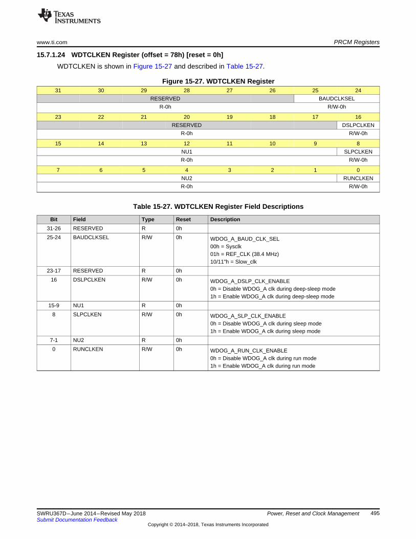
www.ti.com PRCM Registers
495SWRU367D–June 2014–Revised May 2018Submit Documentation Feedback
Copyright © 2014–2018, Texas Instruments Incorporated
Power, Reset and Clock Management
15.7.1.24 WDTCLKEN Register (offset = 78h) [reset = 0h]WDTCLKEN is shown in Figure 15-27 and described in Table 15-27.
Figure 15-27. WDTCLKEN Register31 30 29 28 27 26 25 24
RESERVED BAUDCLKSELR-0h R/W-0h
23 22 21 20 19 18 17 16RESERVED DSLPCLKEN
R-0h R/W-0h
15 14 13 12 11 10 9 8NU1 SLPCLKENR-0h R/W-0h
7 6 5 4 3 2 1 0NU2 RUNCLKENR-0h R/W-0h
Table 15-27. WDTCLKEN Register Field Descriptions
Bit Field Type Reset Description31-26 RESERVED R 0h25-24 BAUDCLKSEL R/W 0h WDOG_A_BAUD_CLK_SEL
00h = Sysclk01h = REF_CLK (38.4 MHz)10/11"h = Slow_clk
23-17 RESERVED R 0h16 DSLPCLKEN R/W 0h WDOG_A_DSLP_CLK_ENABLE
0h = Disable WDOG_A clk during deep-sleep mode1h = Enable WDOG_A clk during deep-sleep mode
15-9 NU1 R 0h8 SLPCLKEN R/W 0h WDOG_A_SLP_CLK_ENABLE
0h = Disable WDOG_A clk during sleep mode1h = Enable WDOG_A clk during sleep mode
7-1 NU2 R 0h0 RUNCLKEN R/W 0h WDOG_A_RUN_CLK_ENABLE
0h = Disable WDOG_A clk during run mode1h = Enable WDOG_A clk during run mode

PRCM Registers www.ti.com
496 SWRU367D–June 2014–Revised May 2018Submit Documentation Feedback
Copyright © 2014–2018, Texas Instruments Incorporated
Power, Reset and Clock Management
15.7.1.25 WDTSWRST Register (offset = 7Ch) [reset = 0h]WDTSWRST is shown in Figure 15-28 and described in Table 15-28.
Figure 15-28. WDTSWRST Register31 30 29 28 27 26 25 24
RESERVEDR-0h
23 22 21 20 19 18 17 16RESERVED
R-0h
15 14 13 12 11 10 9 8RESERVED
R-0h
7 6 5 4 3 2 1 0RESERVED ENSTS SWRST
R-0h R-0h R/W-0h
Table 15-28. WDTSWRST Register Field Descriptions
Bit Field Type Reset Description31-2 RESERVED R 0h
1 ENSTS R 0h WDOG_A_ENABLED_STATUS0h = WDOG_A Clocks and resets are disabled1h = WDOG_A Clocks and resets are enabled
0 SWRST R/W 0h WDOG_A_SOFT_RESET0h = De-assert reset for WDOG_A1h = Assert reset for WDOG_A

www.ti.com PRCM Registers
497SWRU367D–June 2014–Revised May 2018Submit Documentation Feedback
Copyright © 2014–2018, Texas Instruments Incorporated
Power, Reset and Clock Management
15.7.1.26 UART0CLKEN Register (offset = 80h) [reset = 0h]UART0CLKEN is shown in Figure 15-29 and described in Table 15-29.
Figure 15-29. UART0CLKEN Register31 30 29 28 27 26 25 24
RESERVEDR-0h
23 22 21 20 19 18 17 16RESERVED UART0DSLPC
LKENR-0h R/W-0h
15 14 13 12 11 10 9 8NU1 UART0SLPCLK
ENR-0h R/W-0h
7 6 5 4 3 2 1 0NU2 UART0RCLKE
NR-0h R/W-0h
Table 15-29. UART0CLKEN Register Field Descriptions
Bit Field Type Reset Description31-17 RESERVED R 0h
16 UART0DSLPCLKEN R/W 0h UART_A0_DSLP_CLK_ENABLE0h = Disable UART_A0 clk during deep-sleep mode1h = Enable UART_A0 clk during deep-sleep mode
15-9 NU1 R 0h8 UART0SLPCLKEN R/W 0h UART_A0_SLP_CLK_ENABLE
0h = Disable UART_A0 clk during sleep mode1h = Enable UART_A0 clk during sleep mode
7-1 NU2 R 0h0 UART0RCLKEN R/W 0h UART_A0_RUN_CLK_ENABLE
0h = Disable UART_A0 clk during run mode1h = Enable UART_A0 clk during run mode
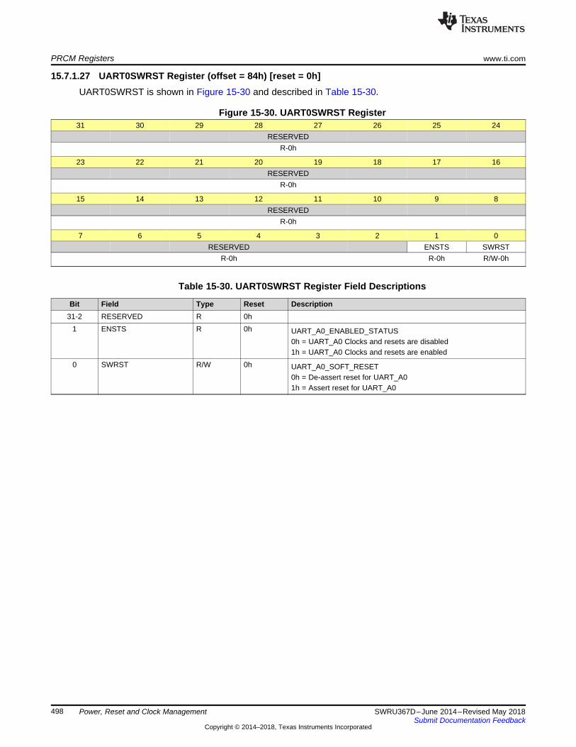
PRCM Registers www.ti.com
498 SWRU367D–June 2014–Revised May 2018Submit Documentation Feedback
Copyright © 2014–2018, Texas Instruments Incorporated
Power, Reset and Clock Management
15.7.1.27 UART0SWRST Register (offset = 84h) [reset = 0h]UART0SWRST is shown in Figure 15-30 and described in Table 15-30.
Figure 15-30. UART0SWRST Register31 30 29 28 27 26 25 24
RESERVEDR-0h
23 22 21 20 19 18 17 16RESERVED
R-0h
15 14 13 12 11 10 9 8RESERVED
R-0h
7 6 5 4 3 2 1 0RESERVED ENSTS SWRST
R-0h R-0h R/W-0h
Table 15-30. UART0SWRST Register Field Descriptions
Bit Field Type Reset Description31-2 RESERVED R 0h
1 ENSTS R 0h UART_A0_ENABLED_STATUS0h = UART_A0 Clocks and resets are disabled1h = UART_A0 Clocks and resets are enabled
0 SWRST R/W 0h UART_A0_SOFT_RESET0h = De-assert reset for UART_A01h = Assert reset for UART_A0

www.ti.com PRCM Registers
499SWRU367D–June 2014–Revised May 2018Submit Documentation Feedback
Copyright © 2014–2018, Texas Instruments Incorporated
Power, Reset and Clock Management
15.7.1.28 UART1CLKEN Register (offset = 88h) [reset = 0h]UART1CLKEN is shown in Figure 15-31 and described in Table 15-31.
Figure 15-31. UART1CLKEN Register31 30 29 28 27 26 25 24
RESERVEDR-0h
23 22 21 20 19 18 17 16RESERVED DSLPCLKEN
R-0h R/W-0h
15 14 13 12 11 10 9 8NU1 SLPCLKENR-0h R/W-0h
7 6 5 4 3 2 1 0NU2 RUNCLKENR-0h R/W-0h
Table 15-31. UART1CLKEN Register Field Descriptions
Bit Field Type Reset Description31-17 RESERVED R 0h
16 DSLPCLKEN R/W 0h UART_A1_DSLP_CLK_ENABLE0h = Disable UART_A1 clk during deep-sleep mode1h = Enable UART_A1 clk during deep-sleep mode
15-9 NU1 R 0h8 SLPCLKEN R/W 0h UART_A1_SLP_CLK_ENABLE
0h = Disable UART_A1 clk during sleep mode1h = Enable UART_A1 clk during sleep mode
7-1 NU2 R 0h0 RUNCLKEN R/W 0h UART_A1_RUN_CLK_ENABLE
0h = Disable UART_A1 clk during run mode1h = Enable UART_A1 clk during run mode
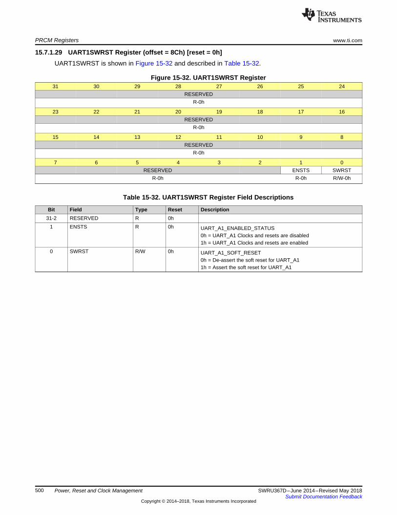
PRCM Registers www.ti.com
500 SWRU367D–June 2014–Revised May 2018Submit Documentation Feedback
Copyright © 2014–2018, Texas Instruments Incorporated
Power, Reset and Clock Management
15.7.1.29 UART1SWRST Register (offset = 8Ch) [reset = 0h]UART1SWRST is shown in Figure 15-32 and described in Table 15-32.
Figure 15-32. UART1SWRST Register31 30 29 28 27 26 25 24
RESERVEDR-0h
23 22 21 20 19 18 17 16RESERVED
R-0h
15 14 13 12 11 10 9 8RESERVED
R-0h
7 6 5 4 3 2 1 0RESERVED ENSTS SWRST
R-0h R-0h R/W-0h
Table 15-32. UART1SWRST Register Field Descriptions
Bit Field Type Reset Description31-2 RESERVED R 0h
1 ENSTS R 0h UART_A1_ENABLED_STATUS0h = UART_A1 Clocks and resets are disabled1h = UART_A1 Clocks and resets are enabled
0 SWRST R/W 0h UART_A1_SOFT_RESET0h = De-assert the soft reset for UART_A11h = Assert the soft reset for UART_A1

www.ti.com PRCM Registers
501SWRU367D–June 2014–Revised May 2018Submit Documentation Feedback
Copyright © 2014–2018, Texas Instruments Incorporated
Power, Reset and Clock Management
15.7.1.30 GPT0CLKCFG Register (offset = 90h) [reset = 0h]GPT0CLKCFG is shown in Figure 15-33 and described in Table 15-33.
Figure 15-33. GPT0CLKCFG Register31 30 29 28 27 26 25 24
RESERVEDR-0h
23 22 21 20 19 18 17 16RESERVED DSLPCLKEN
R-0h R/W-0h
15 14 13 12 11 10 9 8NU1 SLPCLKENR-0h R/W-0h
7 6 5 4 3 2 1 0NU2 RUNCLKENR-0h R/W-0h
Table 15-33. GPT0CLKCFG Register Field Descriptions
Bit Field Type Reset Description31-17 RESERVED R 0h
16 DSLPCLKEN R/W 0h GPT_A0_DSLP_CLK_ENABLE0h = Disable the GPT_A0 clock during deep-sleep1h = Enable the GPT_A0 clock during deep-sleep
15-9 NU1 R 0h8 SLPCLKEN R/W 0h GPT_A0_SLP_CLK_ENABLE
0h = Disable the GPT_A0 clock during sleep1h = Enable the GPT_A0 clock during sleep
7-1 NU2 R 0h0 RUNCLKEN R/W 0h GPT_A0_RUN_CLK_ENABLE
0h = Disable the GPT_A0 clock during run1h = Enable the GPT_A0 clock during run

PRCM Registers www.ti.com
502 SWRU367D–June 2014–Revised May 2018Submit Documentation Feedback
Copyright © 2014–2018, Texas Instruments Incorporated
Power, Reset and Clock Management
15.7.1.31 GPT0SWRST Register (offset = 94h) [reset = 0h]GPT0SWRST is shown in Figure 15-34 and described in Table 15-34.
Figure 15-34. GPT0SWRST Register31 30 29 28 27 26 25 24
RESERVEDR-0h
23 22 21 20 19 18 17 16RESERVED
R-0h
15 14 13 12 11 10 9 8RESERVED
R-0h
7 6 5 4 3 2 1 0RESERVED ENSTS SWRST
R-0h R-0h R/W-0h
Table 15-34. GPT0SWRST Register Field Descriptions
Bit Field Type Reset Description31-2 RESERVED R 0h
1 ENSTS R 0h GPT_A0_ENABLED_STATUS0h = GPT_A0 clocks and resets are disabled1h = GPT_A0 clocks and resets are enabled
0 SWRST R/W 0h GPT_A0_SOFT_RESET0h = De-assert the soft reset for GPT_A01h = Assert the soft reset for GPT_A0

www.ti.com PRCM Registers
503SWRU367D–June 2014–Revised May 2018Submit Documentation Feedback
Copyright © 2014–2018, Texas Instruments Incorporated
Power, Reset and Clock Management
15.7.1.32 GPT1CLKEN Register (offset = 98h) [reset = 0h]GPT1CLKEN is shown in Figure 15-35 and described in Table 15-35.
Figure 15-35. GPT1CLKEN Register31 30 29 28 27 26 25 24
RESERVEDR-0h
23 22 21 20 19 18 17 16RESERVED DSLPCLKEN
R-0h R/W-0h
15 14 13 12 11 10 9 8NU1 SLPCLKENR-0h R/W-0h
7 6 5 4 3 2 1 0NU2 RUNCLKENR-0h R/W-0h
Table 15-35. GPT1CLKEN Register Field Descriptions
Bit Field Type Reset Description31-17 RESERVED R 0h
16 DSLPCLKEN R/W 0h GPT_A1_DSLP_CLK_ENABLE0h = Disable the GPT_A1 clock during deep-sleep1h = Enable the GPT_A1 clock during deep-sleep
15-9 NU1 R 0h8 SLPCLKEN R/W 0h GPT_A1_SLP_CLK_ENABLE
0h = Disable the GPT_A1 clock during sleep1h = Enable the GPT_A1 clock during sleep
7-1 NU2 R 0h0 RUNCLKEN R/W 0h GPT_A1_RUN_CLK_ENABLE
0h = Disable the GPT_A1 clock during run1h = Enable the GPT_A1 clock during run
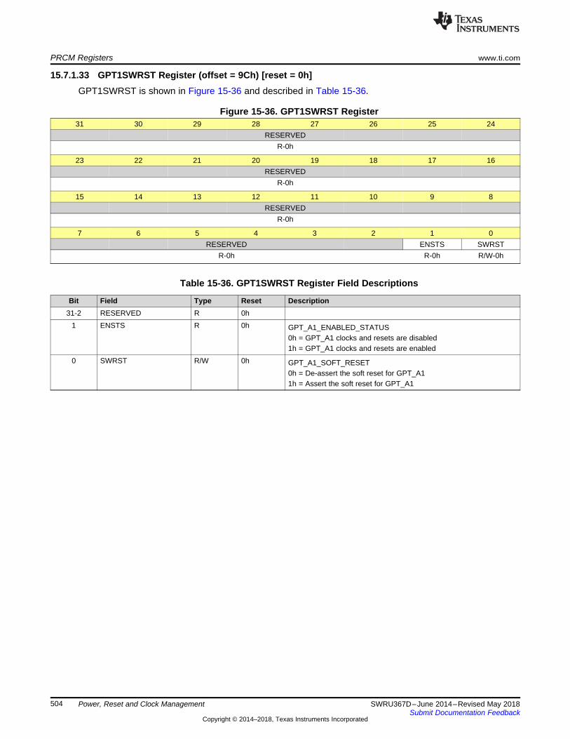
PRCM Registers www.ti.com
504 SWRU367D–June 2014–Revised May 2018Submit Documentation Feedback
Copyright © 2014–2018, Texas Instruments Incorporated
Power, Reset and Clock Management
15.7.1.33 GPT1SWRST Register (offset = 9Ch) [reset = 0h]GPT1SWRST is shown in Figure 15-36 and described in Table 15-36.
Figure 15-36. GPT1SWRST Register31 30 29 28 27 26 25 24
RESERVEDR-0h
23 22 21 20 19 18 17 16RESERVED
R-0h
15 14 13 12 11 10 9 8RESERVED
R-0h
7 6 5 4 3 2 1 0RESERVED ENSTS SWRST
R-0h R-0h R/W-0h
Table 15-36. GPT1SWRST Register Field Descriptions
Bit Field Type Reset Description31-2 RESERVED R 0h
1 ENSTS R 0h GPT_A1_ENABLED_STATUS0h = GPT_A1 clocks and resets are disabled1h = GPT_A1 clocks and resets are enabled
0 SWRST R/W 0h GPT_A1_SOFT_RESET0h = De-assert the soft reset for GPT_A11h = Assert the soft reset for GPT_A1

www.ti.com PRCM Registers
505SWRU367D–June 2014–Revised May 2018Submit Documentation Feedback
Copyright © 2014–2018, Texas Instruments Incorporated
Power, Reset and Clock Management
15.7.1.34 GPT2CLKEN Register (offset = A0h) [reset = 0h]GPT2CLKEN is shown in Figure 15-37 and described in Table 15-37.
Figure 15-37. GPT2CLKEN Register31 30 29 28 27 26 25 24
RESERVEDR-0h
23 22 21 20 19 18 17 16RESERVED DSLPCLKEN
R-0h R/W-0h
15 14 13 12 11 10 9 8NU1 SLPCLKENR-0h R/W-0h
7 6 5 4 3 2 1 0NU2 RUNCLKENR-0h R/W-0h
Table 15-37. GPT2CLKEN Register Field Descriptions
Bit Field Type Reset Description31-17 RESERVED R 0h
16 DSLPCLKEN R/W 0h GPT_A2_DSLP_CLK_ENABLE0h = Disable the GPT_A2 clock during deep-sleep1h = Enable the GPT_A2 clock during deep-sleep
15-9 NU1 R 0h8 SLPCLKEN R/W 0h GPT_A2_SLP_CLK_ENABLE
0h = Disable the GPT_A2 clock during sleep1h = Enable the GPT_A2 clock during sleep
7-1 NU2 R 0h0 RUNCLKEN R/W 0h GPT_A2_RUN_CLK_ENABLE
0h = Disable the GPT_A2 clock during run1h = Enable the GPT_A2 clock during run

PRCM Registers www.ti.com
506 SWRU367D–June 2014–Revised May 2018Submit Documentation Feedback
Copyright © 2014–2018, Texas Instruments Incorporated
Power, Reset and Clock Management
15.7.1.35 GPT2SWRST Register (offset = A4h) [reset = 0h]GPT2SWRST is shown in Figure 15-38 and described in Table 15-38.
Figure 15-38. GPT2SWRST Register31 30 29 28 27 26 25 24
RESERVEDR-0h
23 22 21 20 19 18 17 16RESERVED
R-0h
15 14 13 12 11 10 9 8RESERVED
R-0h
7 6 5 4 3 2 1 0RESERVED ENSTS SWRST
R-0h R-0h R/W-0h
Table 15-38. GPT2SWRST Register Field Descriptions
Bit Field Type Reset Description31-2 RESERVED R 0h
1 ENSTS R 0h GPT_A2_ENABLED_STATUS0h = GPT_A2 clocks and resets are disabled1h = GPT_A2 clocks and resets are enabled
0 SWRST R/W 0h GPT_A2_SOFT_RESET0h = De-assert the soft reset for GPT_A21h = Assert the soft reset for GPT_A2

www.ti.com PRCM Registers
507SWRU367D–June 2014–Revised May 2018Submit Documentation Feedback
Copyright © 2014–2018, Texas Instruments Incorporated
Power, Reset and Clock Management
15.7.1.36 GPT3CLKEN Register (offset = A8h) [reset = 0h]GPT3CLKEN is shown in Figure 15-39 and described in Table 15-39.
Figure 15-39. GPT3CLKEN Register31 30 29 28 27 26 25 24
RESERVEDR-0h
23 22 21 20 19 18 17 16RESERVED DSLPCLKEN
R-0h R/W-0h
15 14 13 12 11 10 9 8NU1 SLPCLKENR-0h R/W-0h
7 6 5 4 3 2 1 0NU2 RUNCLKENR-0h R/W-0h
Table 15-39. GPT3CLKEN Register Field Descriptions
Bit Field Type Reset Description31-17 RESERVED R 0h
16 DSLPCLKEN R/W 0h GPT_A3_DSLP_CLK_ENABLE0h = Disable the GPT_A3 clock during deep-sleep1h = Enable the GPT_A3 clock during deep-sleep
15-9 NU1 R 0h8 SLPCLKEN R/W 0h GPT_A3_SLP_CLK_ENABLE
0h = Disable the GPT_A3 clock during sleep1h = Enable the GPT_A3 clock during sleep
7-1 NU2 R 0h0 RUNCLKEN R/W 0h GPT_A3_RUN_CLK_ENABLE
0h = Disable the GPT_A3 clock during run1h = Enable the GPT_A3 clock during run

PRCM Registers www.ti.com
508 SWRU367D–June 2014–Revised May 2018Submit Documentation Feedback
Copyright © 2014–2018, Texas Instruments Incorporated
Power, Reset and Clock Management
15.7.1.37 GPT3SWRST Register (offset = ACh) [reset = 0h]GPT3SWRST is shown in Figure 15-40 and described in Table 15-40.
Figure 15-40. GPT3SWRST Register31 30 29 28 27 26 25 24
RESERVEDR-0h
23 22 21 20 19 18 17 16RESERVED
R-0h
15 14 13 12 11 10 9 8RESERVED
R-0h
7 6 5 4 3 2 1 0RESERVED ENSTS SWRST
R-0h R-0h R/W-0h
Table 15-40. GPT3SWRST Register Field Descriptions
Bit Field Type Reset Description31-2 RESERVED R 0h
1 ENSTS R 0h GPT_A3_ENABLED_STATUS0h = GPT_A3 Clocks and resets are disabled1h = GPT_A3 Clocks and resets are enabled
0 SWRST R/W 0h GPT_A3_SOFT_RESET0h = De-assert the soft reset for GPT_A31h = Assert the soft reset for GPT_A3
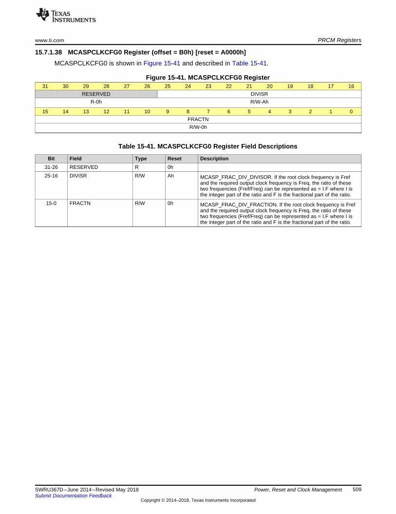
www.ti.com PRCM Registers
509SWRU367D–June 2014–Revised May 2018Submit Documentation Feedback
Copyright © 2014–2018, Texas Instruments Incorporated
Power, Reset and Clock Management
15.7.1.38 MCASPCLKCFG0 Register (offset = B0h) [reset = A0000h]MCASPCLKCFG0 is shown in Figure 15-41 and described in Table 15-41.
Figure 15-41. MCASPCLKCFG0 Register31 30 29 28 27 26 25 24 23 22 21 20 19 18 17 16
RESERVED DIVISRR-0h R/W-Ah
15 14 13 12 11 10 9 8 7 6 5 4 3 2 1 0FRACTNR/W-0h
Table 15-41. MCASPCLKCFG0 Register Field Descriptions
Bit Field Type Reset Description31-26 RESERVED R 0h25-16 DIVISR R/W Ah MCASP_FRAC_DIV_DIVISOR. If the root clock frequency is Fref
and the required output clock frequency is Freq, the ratio of thesetwo frequencies (Fref/Freq) can be represented as = I.F where I isthe integer part of the ratio and F is the fractional part of the ratio.
15-0 FRACTN R/W 0h MCASP_FRAC_DIV_FRACTION. If the root clock frequency is Frefand the required output clock frequency is Freq, the ratio of thesetwo frequencies (Fref/Freq) can be represented as = I.F where I isthe integer part of the ratio and F is the fractional part of the ratio.
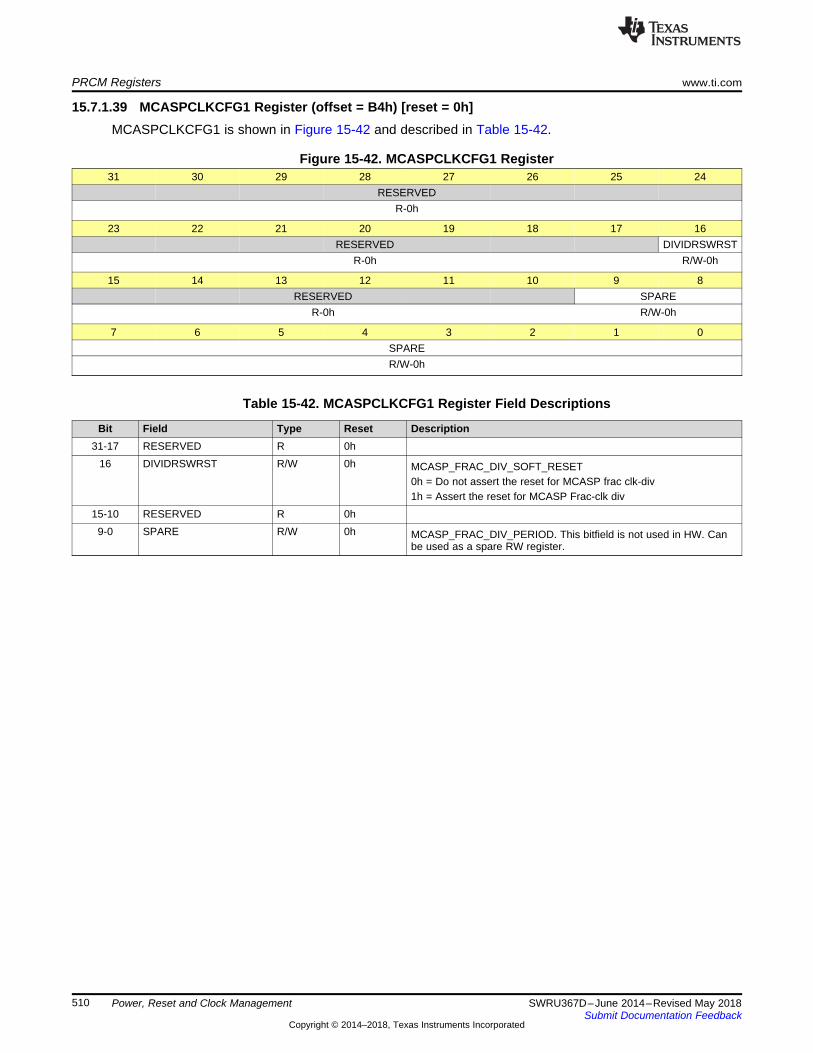
PRCM Registers www.ti.com
510 SWRU367D–June 2014–Revised May 2018Submit Documentation Feedback
Copyright © 2014–2018, Texas Instruments Incorporated
Power, Reset and Clock Management
15.7.1.39 MCASPCLKCFG1 Register (offset = B4h) [reset = 0h]MCASPCLKCFG1 is shown in Figure 15-42 and described in Table 15-42.
Figure 15-42. MCASPCLKCFG1 Register31 30 29 28 27 26 25 24
RESERVEDR-0h
23 22 21 20 19 18 17 16RESERVED DIVIDRSWRST
R-0h R/W-0h
15 14 13 12 11 10 9 8RESERVED SPARE
R-0h R/W-0h
7 6 5 4 3 2 1 0SPARER/W-0h
Table 15-42. MCASPCLKCFG1 Register Field Descriptions
Bit Field Type Reset Description31-17 RESERVED R 0h
16 DIVIDRSWRST R/W 0h MCASP_FRAC_DIV_SOFT_RESET0h = Do not assert the reset for MCASP frac clk-div1h = Assert the reset for MCASP Frac-clk div
15-10 RESERVED R 0h9-0 SPARE R/W 0h MCASP_FRAC_DIV_PERIOD. This bitfield is not used in HW. Can
be used as a spare RW register.
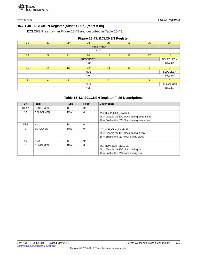
www.ti.com PRCM Registers
511SWRU367D–June 2014–Revised May 2018Submit Documentation Feedback
Copyright © 2014–2018, Texas Instruments Incorporated
Power, Reset and Clock Management
15.7.1.40 I2CLCKEN Register (offset = D8h) [reset = 0h]I2CLCKEN is shown in Figure 15-43 and described in Table 15-43.
Figure 15-43. I2CLCKEN Register31 30 29 28 27 26 25 24
RESERVEDR-0h
23 22 21 20 19 18 17 16RESERVED DSLPCLKEN
R-0h R/W-0h
15 14 13 12 11 10 9 8NU1 SLPCLKENR-0h R/W-0h
7 6 5 4 3 2 1 0NU2 RUNCLKENR-0h R/W-0h
Table 15-43. I2CLCKEN Register Field Descriptions
Bit Field Type Reset Description31-17 RESERVED R 0h
16 DSLPCLKEN R/W 0h I2C_DSLP_CLK_ENABLE0h = Disable the I2C clock during deep-sleep1h = Enable the I2C Clock during deep-sleep
15-9 NU1 R 0h8 SLPCLKEN R/W 0h I2C_SLP_CLK_ENABLE
0h = Disable the I2C clock during sleep1h = Enable the I2C clock during sleep
7-1 NU2 R 0h0 RUNCLKEN R/W 0h I2C_RUN_CLK_ENABLE
0h = Disable the I2C clock during run1h = Enable the I2C clock during run

PRCM Registers www.ti.com
512 SWRU367D–June 2014–Revised May 2018Submit Documentation Feedback
Copyright © 2014–2018, Texas Instruments Incorporated
Power, Reset and Clock Management
15.7.1.41 I2CSWRST Register (offset = DCh) [reset = 0h]I2CSWRST is shown in Figure 15-44 and described in Table 15-44.
Figure 15-44. I2CSWRST Register31 30 29 28 27 26 25 24
RESERVEDR-0h
23 22 21 20 19 18 17 16RESERVED
R-0h
15 14 13 12 11 10 9 8RESERVED
R-0h
7 6 5 4 3 2 1 0RESERVED ENSTS SWRST
R-0h R-0h R/W-0h
Table 15-44. I2CSWRST Register Field Descriptions
Bit Field Type Reset Description31-2 RESERVED R 0h
1 ENSTS R 0h I2C_ENABLED_STATUS0h = I2C clocks and resets are disabled1h = I2C Clocks and resets are enabled
0 SWRST R/W 0h I2C_SOFT_RESET0h = De-assert the soft reset for Shared-I2C1h = Assert the soft reset for Shared-I2C
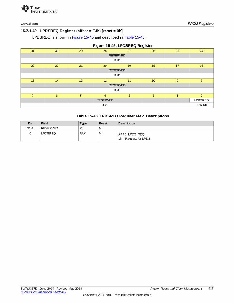
www.ti.com PRCM Registers
513SWRU367D–June 2014–Revised May 2018Submit Documentation Feedback
Copyright © 2014–2018, Texas Instruments Incorporated
Power, Reset and Clock Management
15.7.1.42 LPDSREQ Register (offset = E4h) [reset = 0h]LPDSREQ is shown in Figure 15-45 and described in Table 15-45.
Figure 15-45. LPDSREQ Register31 30 29 28 27 26 25 24
RESERVEDR-0h
23 22 21 20 19 18 17 16RESERVED
R-0h
15 14 13 12 11 10 9 8RESERVED
R-0h
7 6 5 4 3 2 1 0RESERVED LPDSREQ
R-0h R/W-0h
Table 15-45. LPDSREQ Register Field Descriptions
Bit Field Type Reset Description31-1 RESERVED R 0h
0 LPDSREQ R/W 0h APPS_LPDS_REQ1h = Request for LPDS
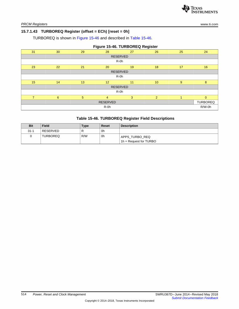
PRCM Registers www.ti.com
514 SWRU367D–June 2014–Revised May 2018Submit Documentation Feedback
Copyright © 2014–2018, Texas Instruments Incorporated
Power, Reset and Clock Management
15.7.1.43 TURBOREQ Register (offset = ECh) [reset = 0h]TURBOREQ is shown in Figure 15-46 and described in Table 15-46.
Figure 15-46. TURBOREQ Register31 30 29 28 27 26 25 24
RESERVEDR-0h
23 22 21 20 19 18 17 16RESERVED
R-0h
15 14 13 12 11 10 9 8RESERVED
R-0h
7 6 5 4 3 2 1 0RESERVED TURBOREQ
R-0h R/W-0h
Table 15-46. TURBOREQ Register Field Descriptions
Bit Field Type Reset Description31-1 RESERVED R 0h
0 TURBOREQ R/W 0h APPS_TURBO_REQ1h = Request for TURBO
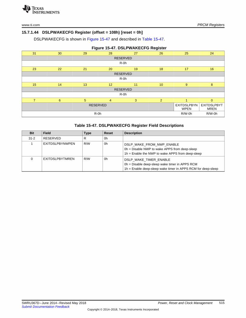
www.ti.com PRCM Registers
515SWRU367D–June 2014–Revised May 2018Submit Documentation Feedback
Copyright © 2014–2018, Texas Instruments Incorporated
Power, Reset and Clock Management
15.7.1.44 DSLPWAKECFG Register (offset = 108h) [reset = 0h]DSLPWAKECFG is shown in Figure 15-47 and described in Table 15-47.
Figure 15-47. DSLPWAKECFG Register31 30 29 28 27 26 25 24
RESERVEDR-0h
23 22 21 20 19 18 17 16RESERVED
R-0h
15 14 13 12 11 10 9 8RESERVED
R-0h
7 6 5 4 3 2 1 0RESERVED EXITDSLPBYN
WPENEXITDSLPBYT
MRENR-0h R/W-0h R/W-0h
Table 15-47. DSLPWAKECFG Register Field Descriptions
Bit Field Type Reset Description31-2 RESERVED R 0h
1 EXITDSLPBYNWPEN R/W 0h DSLP_WAKE_FROM_NWP_ENABLE0h = Disable NWP to wake APPS from deep-sleep1h = Enable the NWP to wake APPS from deep-sleep
0 EXITDSLPBYTMREN R/W 0h DSLP_WAKE_TIMER_ENABLE0h = Disable deep-sleep wake timer in APPS RCM1h = Enable deep-sleep wake timer in APPS RCM for deep-sleep
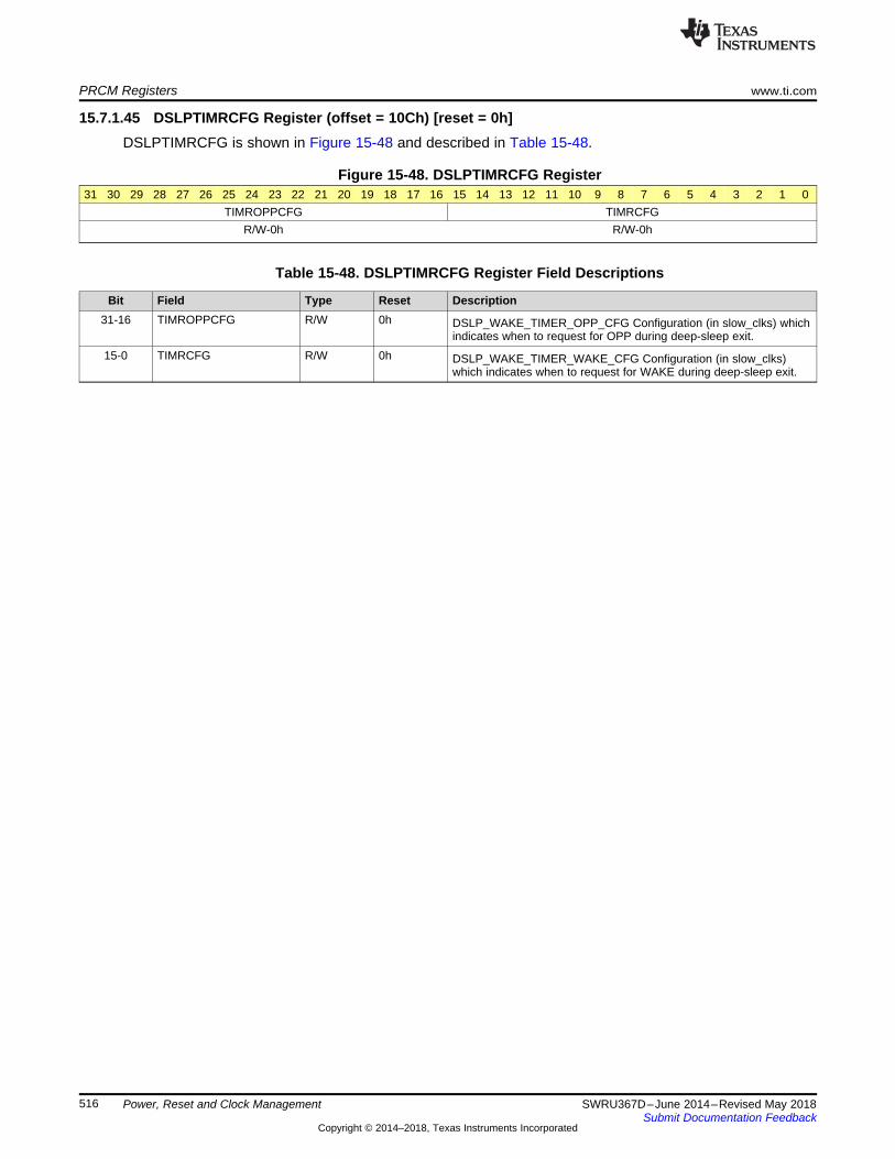
PRCM Registers www.ti.com
516 SWRU367D–June 2014–Revised May 2018Submit Documentation Feedback
Copyright © 2014–2018, Texas Instruments Incorporated
Power, Reset and Clock Management
15.7.1.45 DSLPTIMRCFG Register (offset = 10Ch) [reset = 0h]DSLPTIMRCFG is shown in Figure 15-48 and described in Table 15-48.
Figure 15-48. DSLPTIMRCFG Register31 30 29 28 27 26 25 24 23 22 21 20 19 18 17 16 15 14 13 12 11 10 9 8 7 6 5 4 3 2 1 0
TIMROPPCFG TIMRCFGR/W-0h R/W-0h
Table 15-48. DSLPTIMRCFG Register Field Descriptions
Bit Field Type Reset Description31-16 TIMROPPCFG R/W 0h DSLP_WAKE_TIMER_OPP_CFG Configuration (in slow_clks) which
indicates when to request for OPP during deep-sleep exit.15-0 TIMRCFG R/W 0h DSLP_WAKE_TIMER_WAKE_CFG Configuration (in slow_clks)
which indicates when to request for WAKE during deep-sleep exit.
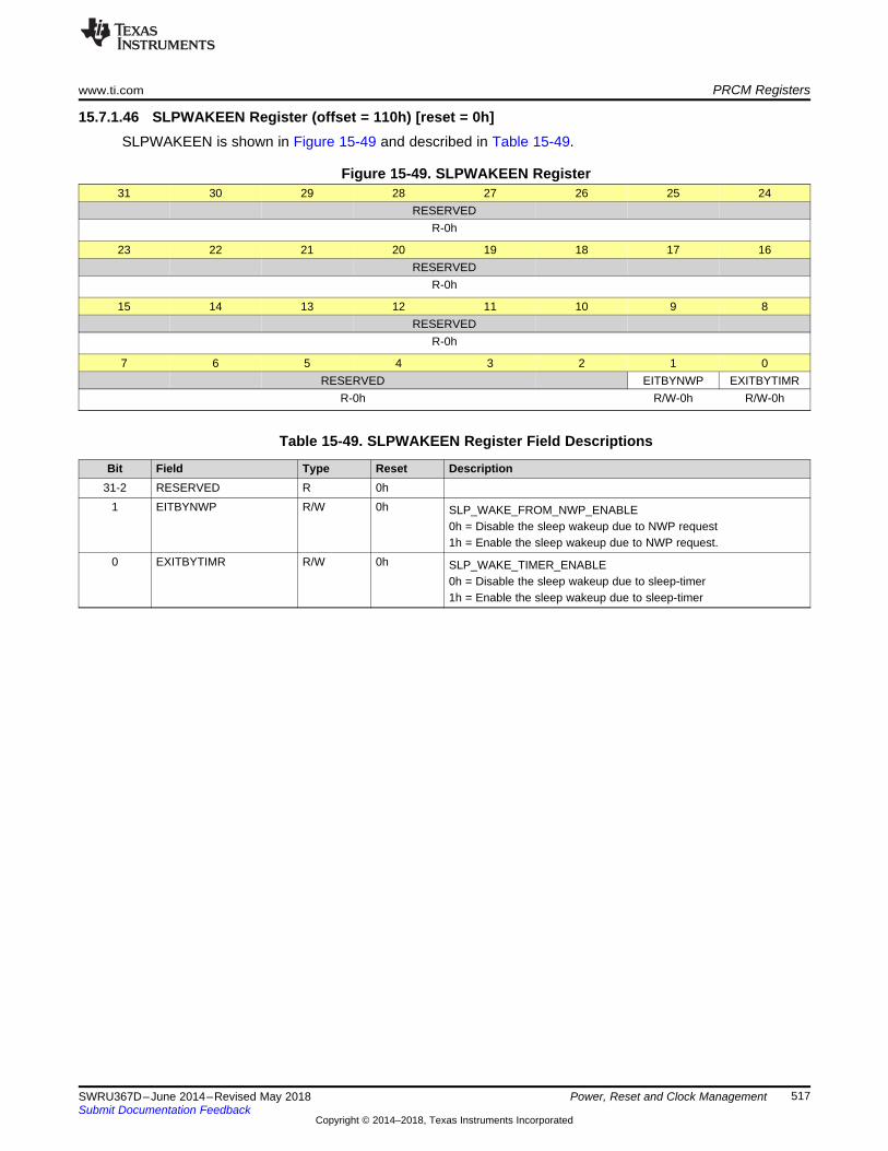
www.ti.com PRCM Registers
517SWRU367D–June 2014–Revised May 2018Submit Documentation Feedback
Copyright © 2014–2018, Texas Instruments Incorporated
Power, Reset and Clock Management
15.7.1.46 SLPWAKEEN Register (offset = 110h) [reset = 0h]SLPWAKEEN is shown in Figure 15-49 and described in Table 15-49.
Figure 15-49. SLPWAKEEN Register31 30 29 28 27 26 25 24
RESERVEDR-0h
23 22 21 20 19 18 17 16RESERVED
R-0h
15 14 13 12 11 10 9 8RESERVED
R-0h
7 6 5 4 3 2 1 0RESERVED EITBYNWP EXITBYTIMR
R-0h R/W-0h R/W-0h
Table 15-49. SLPWAKEEN Register Field Descriptions
Bit Field Type Reset Description31-2 RESERVED R 0h
1 EITBYNWP R/W 0h SLP_WAKE_FROM_NWP_ENABLE0h = Disable the sleep wakeup due to NWP request1h = Enable the sleep wakeup due to NWP request.
0 EXITBYTIMR R/W 0h SLP_WAKE_TIMER_ENABLE0h = Disable the sleep wakeup due to sleep-timer1h = Enable the sleep wakeup due to sleep-timer
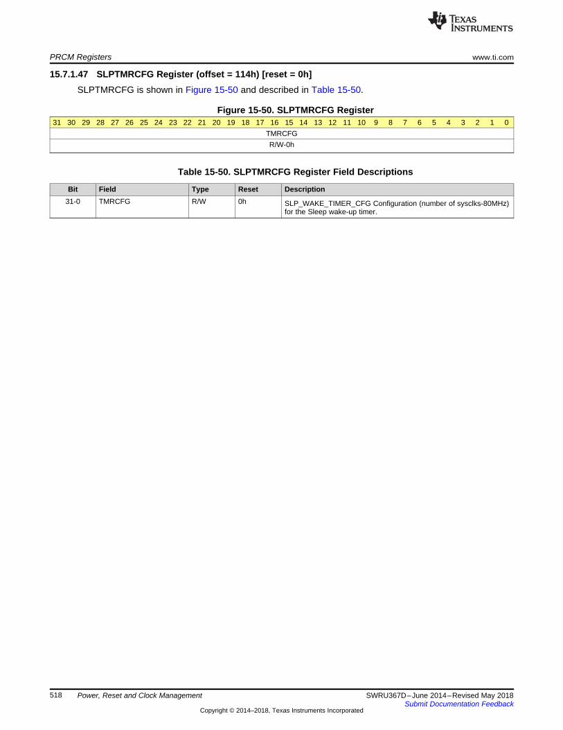
PRCM Registers www.ti.com
518 SWRU367D–June 2014–Revised May 2018Submit Documentation Feedback
Copyright © 2014–2018, Texas Instruments Incorporated
Power, Reset and Clock Management
15.7.1.47 SLPTMRCFG Register (offset = 114h) [reset = 0h]SLPTMRCFG is shown in Figure 15-50 and described in Table 15-50.
Figure 15-50. SLPTMRCFG Register31 30 29 28 27 26 25 24 23 22 21 20 19 18 17 16 15 14 13 12 11 10 9 8 7 6 5 4 3 2 1 0
TMRCFGR/W-0h
Table 15-50. SLPTMRCFG Register Field Descriptions
Bit Field Type Reset Description31-0 TMRCFG R/W 0h SLP_WAKE_TIMER_CFG Configuration (number of sysclks-80MHz)
for the Sleep wake-up timer.
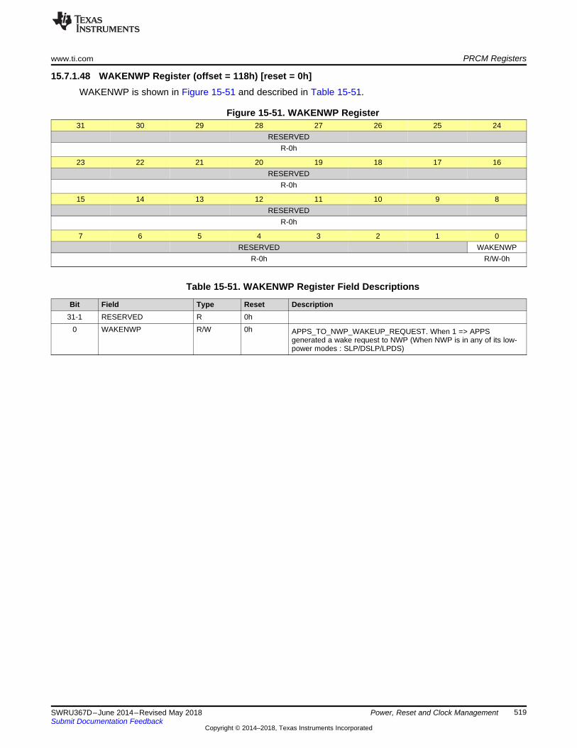
www.ti.com PRCM Registers
519SWRU367D–June 2014–Revised May 2018Submit Documentation Feedback
Copyright © 2014–2018, Texas Instruments Incorporated
Power, Reset and Clock Management
15.7.1.48 WAKENWP Register (offset = 118h) [reset = 0h]WAKENWP is shown in Figure 15-51 and described in Table 15-51.
Figure 15-51. WAKENWP Register31 30 29 28 27 26 25 24
RESERVEDR-0h
23 22 21 20 19 18 17 16RESERVED
R-0h
15 14 13 12 11 10 9 8RESERVED
R-0h
7 6 5 4 3 2 1 0RESERVED WAKENWP
R-0h R/W-0h
Table 15-51. WAKENWP Register Field Descriptions
Bit Field Type Reset Description31-1 RESERVED R 0h
0 WAKENWP R/W 0h APPS_TO_NWP_WAKEUP_REQUEST. When 1 => APPSgenerated a wake request to NWP (When NWP is in any of its low-power modes : SLP/DSLP/LPDS)
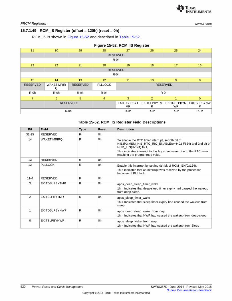
PRCM Registers www.ti.com
520 SWRU367D–June 2014–Revised May 2018Submit Documentation Feedback
Copyright © 2014–2018, Texas Instruments Incorporated
Power, Reset and Clock Management
15.7.1.49 RCM_IS Register (offset = 120h) [reset = 0h]RCM_IS is shown in Figure 15-52 and described in Table 15-52.
Figure 15-52. RCM_IS Register31 30 29 28 27 26 25 24
RESERVEDR-0h
23 22 21 20 19 18 17 16RESERVED
R-0h
15 14 13 12 11 10 9 8RESERVED WAKETIMRIR
QRESERVED PLLLOCK RESERVED
R-0h R-0h R-0h R-0h R-0h
7 6 5 4 3 2 1 0RESERVED EXITDSLPBYT
MREXITSLPBYTM
REXITDSLPBYN
WPEXITSLPBYNW
PR-0h R-0h R-0h R-0h R-0h
Table 15-52. RCM_IS Register Field Descriptions
Bit Field Type Reset Description31-15 RESERVED R 0h
14 WAKETIMRIRQ R 0h To enable the RTC timer interrupt, set 0th bit ofHIB3P3:MEM_HIB_RTC_IRQ_ENABLE(0x4402 F854) and 2nd bit ofRCM_IEN(0x124) to 1,1h = indicates interrupt to the Apps processor due to the RTC timerreaching the programmed value.
13 RESERVED R 0h12 PLLLOCK R 0h Enable this interrupt by setting 0th bit of RCM_IEN(0x124).
1h = indicates that an interrupt was received by the processorbecause of PLL lock.
11-4 RESERVED R 0h3 EXITDSLPBYTMR R 0h apps_deep_sleep_timer_wake
1h = Indicates that deep-sleep timer expiry had caused the wakeupfrom deep-sleep.
2 EXITSLPBYTMR R 0h apps_sleep_timer_wake1h = Indicates that sleep timer expiry had caused the wakeup fromsleep.
1 EXITDSLPBYNWP R 0h apps_deep_sleep_wake_from_nwp1h = Indicates that NWP had caused the wakeup from deep-sleep.
0 EXITSLPBYNWP R 0h apps_sleep_wake_from_nwp1h = Indicates that NWP had caused the wakeup from Sleep
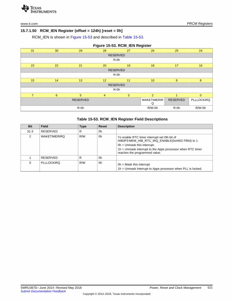
www.ti.com PRCM Registers
521SWRU367D–June 2014–Revised May 2018Submit Documentation Feedback
Copyright © 2014–2018, Texas Instruments Incorporated
Power, Reset and Clock Management
15.7.1.50 RCM_IEN Register (offset = 124h) [reset = 0h]RCM_IEN is shown in Figure 15-53 and described in Table 15-53.
Figure 15-53. RCM_IEN Register31 30 29 28 27 26 25 24
RESERVEDR-0h
23 22 21 20 19 18 17 16RESERVED
R-0h
15 14 13 12 11 10 9 8RESERVED
R-0h
7 6 5 4 3 2 1 0RESERVED WAKETIMERIR
QRESERVED PLLLOCKIRQ
R-0h R/W-0h R-0h R/W-0h
Table 15-53. RCM_IEN Register Field Descriptions
Bit Field Type Reset Description31-3 RESERVED R 0h
2 WAKETIMERIRQ R/W 0h To enable RTC timer interrupt set 0th bit ofHIB3P3:MEM_HIB_RTC_IRQ_ENABLE(0x4402 F854) to 10h = Unmask this interrupt.1h = Unmask interrupt to the Apps processor when RTC timerreaches the programmed value.
1 RESERVED R 0h0 PLLLOCKIRQ R/W 0h 0h = Mask this interrupt
1h = Unmask Interrupt to Apps processor when PLL is locked.
522 SWRU367D–June 2014–Revised May 2018Submit Documentation Feedback
Copyright © 2014–2018, Texas Instruments Incorporated
I/O Pads and Pin Multiplexing
Chapter 16SWRU367D–June 2014–Revised May 2018
I/O Pads and Pin Multiplexing
Topic ........................................................................................................................... Page
16.1 Overview ......................................................................................................... 52316.2 I/O Pad Electrical Specifications......................................................................... 52316.3 Analog-Digital Pin Multiplexing .......................................................................... 52516.4 Special Ana/DIG Pins ........................................................................................ 52616.5 Analog Mux Control Registers ........................................................................... 52816.6 Pins Available for Applications .......................................................................... 53016.7 Functional Pin Mux Configurations..................................................................... 53216.8 Pin Mapping Recommendations ......................................................................... 546
www.ti.com Overview
523SWRU367D–June 2014–Revised May 2018Submit Documentation Feedback
Copyright © 2014–2018, Texas Instruments Incorporated
I/O Pads and Pin Multiplexing
16.1 OverviewThe CC3200 features flexible wide-voltage I/Os. Supported features are:• Programmable drive strength from 2 mA to 14 mA (nominal condition) in steps of 2 mA.• Open drain mode• Output buffer isolation• Automatic output isolation during reset and hibernate• Configurable pullup and pulldown (10-uA nominal)• Software configurable pad state retention during LPDS
Each I/O pad cell in the CC3200 has the following ports:• PAD: I/O pad connected to package pin and external components• ODI: Level-shifted data from from PAD to core logic• IDO: Input to I/O-cell from core.• ioden: When level 1, this disables the PMOS xtors of the output stages, making them open-drain type.
For example, I2C may use a open-drain configuration. Value gets latched at the rising edge of RET33.• ioe_n: If level 0, this enables the IDO to PAD path. Otherwise, PAD is tristated (except for the PU/PD,
which are independent).• ioen33: This control signal is driven by hibernate controller. Level 1 enables the IDO to PAD path.
Otherwise, PAD is made Hi-Z (except for the PU/PD, which are independent). This is automaticallycontrolled by hardware to Hi-Z; the main o/p drivers during chip reset (nRESET=0). On first timepower-up, the chip performs a sense-on-power detection of board-level pullup and pulldown resistorson three specific device pins (SOP0, SOP1, and SOP2); after this is done, this control signal is madehigh. The user-defined I/O pads still remain in Hi-Z state until configured by the user program.
• 3-bit drive strength control (value gets latched at rising edge of RET33):– i2maen: Level 1 enables the approximately 2-mA output stage (in parallel with 4-mA and 8-mA
drivers, if enabled)– i4maen: Level 1 enables the approximately 4-mA output stage (in parallel with 2-mA and 8-mA
drivers, if enabled)– i8maen: Level 1 enables the approximately 8-mA output stage (in parallel with 4-mA and 2-mA
drivers, if enabled)
NOTE: Any drive strength between 2 mA and 14 mA can be realized by enabling one or more ofabove drivers together. Treat these 3 pins as 3-bit binary-coded strength control.
• Pullup and pulldown controls (value gets latched at rising edge of RET33. Works independent of these:ioe_n, ioen33, i2maen/i4maen/i8maen)– iwkpuen: 10-uA pull up (NOM_25C_3.3V)– iwkpden: 10-uA pull down (NOM_25C_3.3V)
• RET33: Control signal from hibernate controller module. Puts the I/O in low power retention mode. Thecontrol and data signals are latched on rising edge (except ioen33). The internal bias for high-speedlevel-shifter is automatically disabled when RET33 is 1. By default, this signal is controlled by thepower management state machine in the hibernate controller. By default, this signal goes high on entryto hibernate mode. On exit from hibernate, RET33 returns to level 0 to allow the device firmware andapplication software to access the I/O pads.
16.2 I/O Pad Electrical Specifications
Table 16-1. GPIO Pin Electrical Specifications (25 C)(Except Pin 29, 30, 45, 50, 52 , 53)
GPIO Pin Electrical Specifications (25 C)(Except Pin 29, 30, 45, 50, 52 , 53)Parameter Parameter Name Min Nom Max Unit
CIN Pin capacitance 4 pF
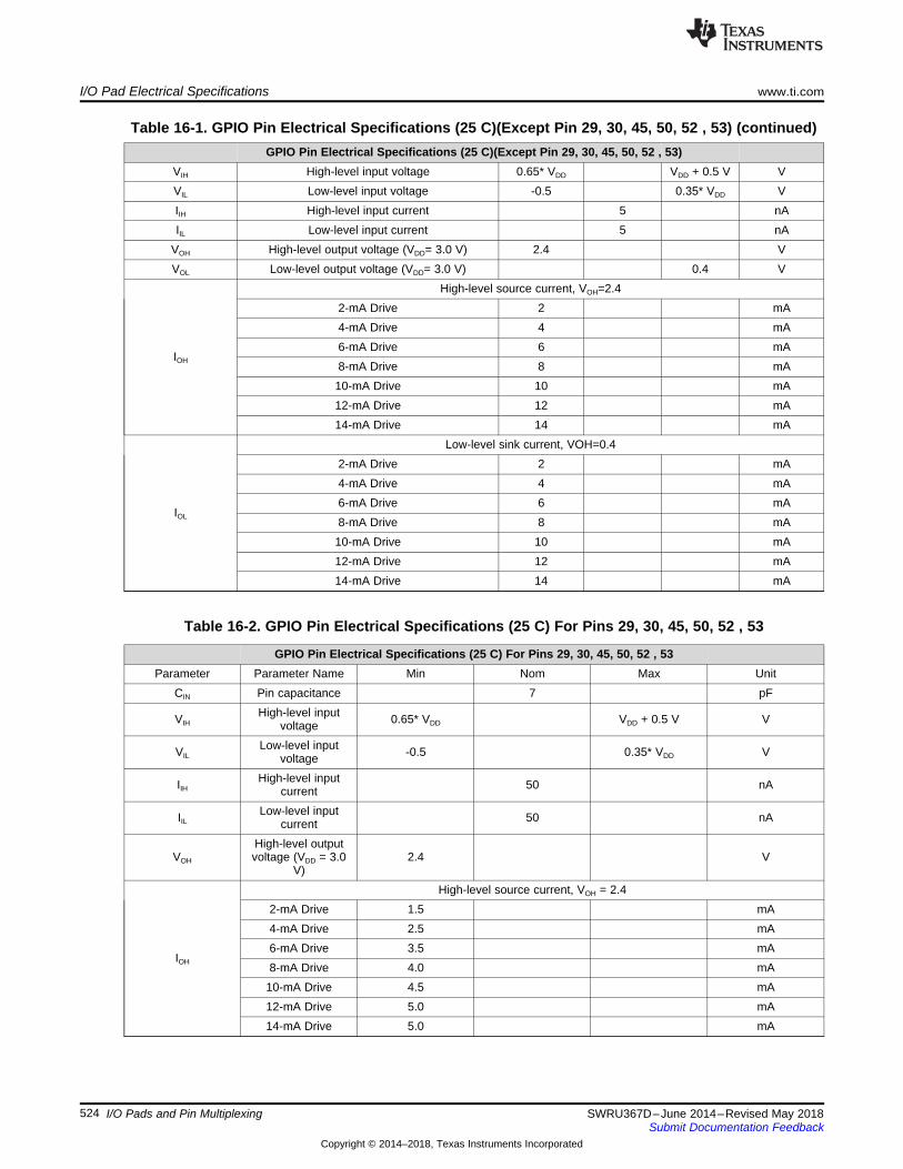
I/O Pad Electrical Specifications www.ti.com
524 SWRU367D–June 2014–Revised May 2018Submit Documentation Feedback
Copyright © 2014–2018, Texas Instruments Incorporated
I/O Pads and Pin Multiplexing
Table 16-1. GPIO Pin Electrical Specifications (25 C)(Except Pin 29, 30, 45, 50, 52 , 53) (continued)GPIO Pin Electrical Specifications (25 C)(Except Pin 29, 30, 45, 50, 52 , 53)
VIH High-level input voltage 0.65* VDD VDD + 0.5 V VVIL Low-level input voltage -0.5 0.35* VDD VIIH High-level input current 5 nAIIL Low-level input current 5 nA
VOH High-level output voltage (VDD= 3.0 V) 2.4 VVOL Low-level output voltage (VDD= 3.0 V) 0.4 V
IOH
High-level source current, VOH=2.42-mA Drive 2 mA4-mA Drive 4 mA6-mA Drive 6 mA8-mA Drive 8 mA10-mA Drive 10 mA12-mA Drive 12 mA14-mA Drive 14 mA
IOL
Low-level sink current, VOH=0.42-mA Drive 2 mA4-mA Drive 4 mA6-mA Drive 6 mA8-mA Drive 8 mA10-mA Drive 10 mA12-mA Drive 12 mA14-mA Drive 14 mA
Table 16-2. GPIO Pin Electrical Specifications (25 C) For Pins 29, 30, 45, 50, 52 , 53
GPIO Pin Electrical Specifications (25 C) For Pins 29, 30, 45, 50, 52 , 53Parameter Parameter Name Min Nom Max Unit
CIN Pin capacitance 7 pF
VIHHigh-level input
voltage 0.65* VDD VDD + 0.5 V V
VILLow-level input
voltage -0.5 0.35* VDD V
IIHHigh-level input
current 50 nA
IILLow-level input
current 50 nA
VOH
High-level outputvoltage (VDD = 3.0
V)2.4 V
IOH
High-level source current, VOH = 2.42-mA Drive 1.5 mA4-mA Drive 2.5 mA6-mA Drive 3.5 mA8-mA Drive 4.0 mA
10-mA Drive 4.5 mA12-mA Drive 5.0 mA14-mA Drive 5.0 mA
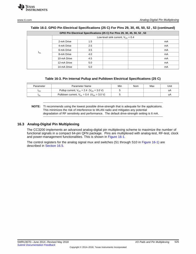
www.ti.com Analog-Digital Pin Multiplexing
525SWRU367D–June 2014–Revised May 2018Submit Documentation Feedback
Copyright © 2014–2018, Texas Instruments Incorporated
I/O Pads and Pin Multiplexing
Table 16-2. GPIO Pin Electrical Specifications (25 C) For Pins 29, 30, 45, 50, 52 , 53 (continued)GPIO Pin Electrical Specifications (25 C) For Pins 29, 30, 45, 50, 52 , 53
IOL
Low-level sink current, VOH = 0.42-mA Drive 1.5 mA4-mA Drive 2.5 mA6-mA Drive 3.5 mA8-mA Drive 4.0 mA
10-mA Drive 4.5 mA12-mA Drive 5.0 mA14-mA Drive 5.0 mA
Table 16-3. Pin Internal Pullup and Pulldown Electrical Specifications (25 C)
Parameter Parameter Name Min Nom Max UnitIOH Pullup current, VOH = 2.4 (VDD = 3.0 V) 5 uAIOL Pulldown current, VOL = 0.4 (VDD = 3.0 V) 5 uA
NOTE: TI recommends using the lowest possible drive-strength that is adequate for the applications.This minimizes the risk of interference to WLAN radio and mitigates any potentialdegradation of RF sensitivity and performance. The default drive-strength setting is 6 mA.
16.3 Analog-Digital Pin MultiplexingThe CC3200 implements an advanced analog-digital pin multiplexing scheme to maximize the number offunctional signals in a compact 64-pin QFN package. Pins are multiplexed with analog-test, RF-test, clockand power-management functionalities. This is shown in Figure 16-1.
The control registers for the analog signal mux and switches (S1 through S10 in Figure 16-1) aredescribed in Section 16.5.
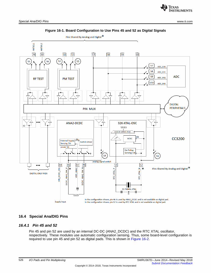
Special Ana/DIG Pins www.ti.com
526 SWRU367D–June 2014–Revised May 2018Submit Documentation Feedback
Copyright © 2014–2018, Texas Instruments Incorporated
I/O Pads and Pin Multiplexing
Figure 16-1. Board Configuration to Use Pins 45 and 52 as Digital Signals
16.4 Special Ana/DIG Pins
16.4.1 Pin 45 and 52Pin 45 and pin 52 are used by an internal DC-DC (ANA2_DCDC) and the RTC XTAL oscillator,respectively. These modules use automatic configuration sensing. Thus, some board-level configuration isrequired to use pin 45 and pin 52 as digital pads. This is shown in Figure 16-2.
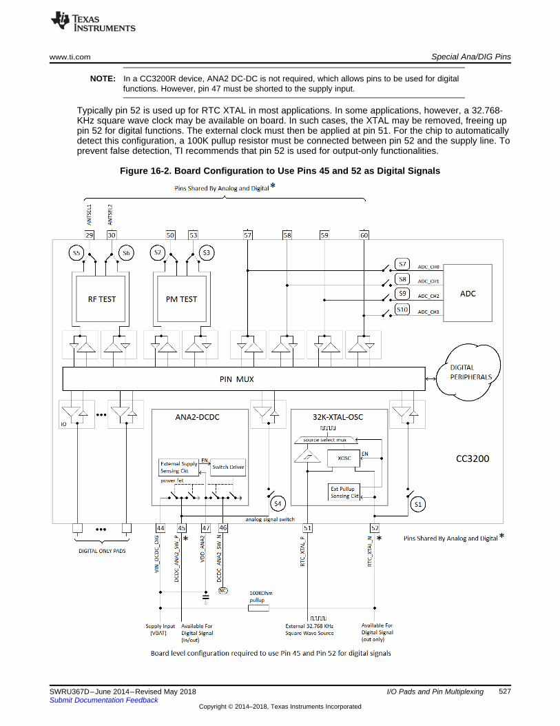
www.ti.com Special Ana/DIG Pins
527SWRU367D–June 2014–Revised May 2018Submit Documentation Feedback
Copyright © 2014–2018, Texas Instruments Incorporated
I/O Pads and Pin Multiplexing
NOTE: In a CC3200R device, ANA2 DC-DC is not required, which allows pins to be used for digitalfunctions. However, pin 47 must be shorted to the supply input.
Typically pin 52 is used up for RTC XTAL in most applications. In some applications, however, a 32.768-KHz square wave clock may be available on board. In such cases, the XTAL may be removed, freeing uppin 52 for digital functions. The external clock must then be applied at pin 51. For the chip to automaticallydetect this configuration, a 100K pullup resistor must be connected between pin 52 and the supply line. Toprevent false detection, TI recommends that pin 52 is used for output-only functionalities.
Figure 16-2. Board Configuration to Use Pins 45 and 52 as Digital Signals
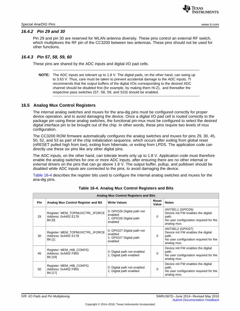
Special Ana/DIG Pins www.ti.com
528 SWRU367D–June 2014–Revised May 2018Submit Documentation Feedback
Copyright © 2014–2018, Texas Instruments Incorporated
I/O Pads and Pin Multiplexing
16.4.2 Pin 29 and 30Pin 29 and pin 30 are reserved for WLAN antenna diversity. These pins control an external RF switch,which multiplexes the RF pin of the CC3200 between two antennas. These pins should not be used forother functions.
16.4.3 Pin 57, 58, 59, 60These pins are shared by the ADC inputs and digital I/O pad cells.
NOTE: The ADC inputs are tolerant up to 1.8 V. The digital pads, on the other hand, can swing upto 3.63 V. Thus, care must be taken to prevent accidental damage to the ADC inputs. TIrecommends that the output buffers of the digital I/Os corresponding to the desired ADCchannel should be disabled first (for example, by making them Hi-Z), and thereafter therespective pass switches (S7, S8, S9, and S10) should be enabled.
16.5 Analog Mux Control RegistersThe internal analog switches and muxes for the ana-dig pins must be configured correctly for properdevice operation, and to avoid damaging the device. Once a digital I/O pad cell is routed correctly to thepackage pin using these analog switches, the functional pin-mux must be configured to select the desireddigital interface pin to be brought out of the chip. In other words, these pins require two levels of muxconfiguration.
The CC3200 ROM firmware automatically configures the analog switches and muxes for pins 29, 30, 45,50, 52, and 53 as part of the chip initialization sequence, which occurs after exiting from global reset(nRESET pulled high from low), exiting from hibernate, or exiting from LPDS. The application code candirectly use these six pins like any other digital pins.
The ADC inputs, on the other hand, can tolerate levels only up to 1.8 V. Application code must thereforeenable the analog switches for one or more ADC inputs, after ensuring there are no other internal orexternal drivers on the pins that can go above 1.8 V. The output buffer, pullup, and pulldown should bedisabled while ADC inputs are connected to the pins, to avoid damaging the device.
Table 16-4 describes the register bits used to configure the internal analog switches and muxes for theana-dig pins.
Table 16-4. Analog Mux Control Registers and Bits
Analog Mux Control Registers and Bits
Pin Analog Mux Control Register and Bit Write Values ResetValue Notes
29Register: MEM_TOPMUXCTRL_IFORCEAddress: 0x4402 E178Bit [0]
0: GPIO26 Digital path notenabled1: GPIO26 Digital pathenabled
0
ANTSEL1 (GPIO26)Device init FW enables the digitalpath.No user configuration required for theanalog mux.
30Register: MEM_TOPMUXCTRL_IFORCEAddress: 0x4402 E178Bit [1]
0: GPIO27 Digital path notenabled1: GPIO27 Digital pathenabled
0
ANTSEL2 (GPIO27)Device init FW enables the digitalpath.No user configuration required for theanalog mux.
45Register: MEM_HIB_CONFIGAddress: 0x4402 F850Bit [19]
0: Digital path not enabled1: Digital path enabled 0
Device init FW enables the digitalpath.No user configuration required for theanalog mux.
50Register: MEM_HIB_CONFIGAddress: 0x4402 F850Bit [17]
0: Digital path not enabled1: Digital path enabled 0
Device init FW enables the digitalpath.No user configuration required for theanalog mux.
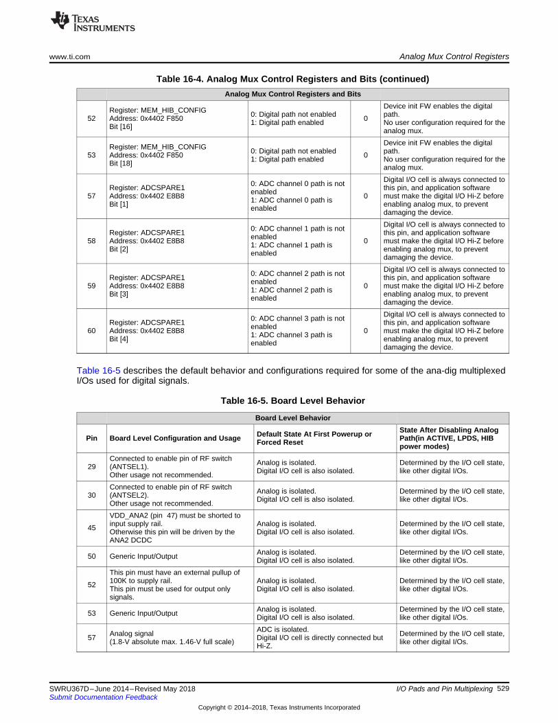
www.ti.com Analog Mux Control Registers
529SWRU367D–June 2014–Revised May 2018Submit Documentation Feedback
Copyright © 2014–2018, Texas Instruments Incorporated
I/O Pads and Pin Multiplexing
Table 16-4. Analog Mux Control Registers and Bits (continued)Analog Mux Control Registers and Bits
52Register: MEM_HIB_CONFIGAddress: 0x4402 F850Bit [16]
0: Digital path not enabled1: Digital path enabled 0
Device init FW enables the digitalpath.No user configuration required for theanalog mux.
53Register: MEM_HIB_CONFIGAddress: 0x4402 F850Bit [18]
0: Digital path not enabled1: Digital path enabled 0
Device init FW enables the digitalpath.No user configuration required for theanalog mux.
57Register: ADCSPARE1Address: 0x4402 E8B8Bit [1]
0: ADC channel 0 path is notenabled1: ADC channel 0 path isenabled
0
Digital I/O cell is always connected tothis pin, and application softwaremust make the digital I/O Hi-Z beforeenabling analog mux, to preventdamaging the device.
58Register: ADCSPARE1Address: 0x4402 E8B8Bit [2]
0: ADC channel 1 path is notenabled1: ADC channel 1 path isenabled
0
Digital I/O cell is always connected tothis pin, and application softwaremust make the digital I/O Hi-Z beforeenabling analog mux, to preventdamaging the device.
59Register: ADCSPARE1Address: 0x4402 E8B8Bit [3]
0: ADC channel 2 path is notenabled1: ADC channel 2 path isenabled
0
Digital I/O cell is always connected tothis pin, and application softwaremust make the digital I/O Hi-Z beforeenabling analog mux, to preventdamaging the device.
60Register: ADCSPARE1Address: 0x4402 E8B8Bit [4]
0: ADC channel 3 path is notenabled1: ADC channel 3 path isenabled
0
Digital I/O cell is always connected tothis pin, and application softwaremust make the digital I/O Hi-Z beforeenabling analog mux, to preventdamaging the device.
Table 16-5 describes the default behavior and configurations required for some of the ana-dig multiplexedI/Os used for digital signals.
Table 16-5. Board Level Behavior
Board Level Behavior
Pin Board Level Configuration and Usage Default State At First Powerup orForced Reset
State After Disabling AnalogPath(in ACTIVE, LPDS, HIBpower modes)
29Connected to enable pin of RF switch(ANTSEL1).Other usage not recommended.
Analog is isolated.Digital I/O cell is also isolated.
Determined by the I/O cell state,like other digital I/Os.
30Connected to enable pin of RF switch(ANTSEL2).Other usage not recommended.
Analog is isolated.Digital I/O cell is also isolated.
Determined by the I/O cell state,like other digital I/Os.
45
VDD_ANA2 (pin 47) must be shorted toinput supply rail.Otherwise this pin will be driven by theANA2 DCDC
Analog is isolated.Digital I/O cell is also isolated.
Determined by the I/O cell state,like other digital I/Os.
50 Generic Input/Output Analog is isolated.Digital I/O cell is also isolated.
Determined by the I/O cell state,like other digital I/Os.
52
This pin must have an external pullup of100K to supply rail.This pin must be used for output onlysignals.
Analog is isolated.Digital I/O cell is also isolated.
Determined by the I/O cell state,like other digital I/Os.
53 Generic Input/Output Analog is isolated.Digital I/O cell is also isolated.
Determined by the I/O cell state,like other digital I/Os.
57 Analog signal(1.8-V absolute max. 1.46-V full scale)
ADC is isolated.Digital I/O cell is directly connected butHi-Z.
Determined by the I/O cell state,like other digital I/Os.
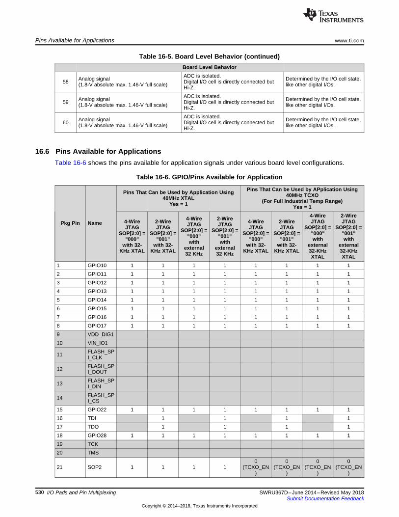
Pins Available for Applications www.ti.com
530 SWRU367D–June 2014–Revised May 2018Submit Documentation Feedback
Copyright © 2014–2018, Texas Instruments Incorporated
I/O Pads and Pin Multiplexing
Table 16-5. Board Level Behavior (continued)Board Level Behavior
58 Analog signal(1.8-V absolute max. 1.46-V full scale)
ADC is isolated.Digital I/O cell is directly connected butHi-Z.
Determined by the I/O cell state,like other digital I/Os.
59 Analog signal(1.8-V absolute max. 1.46-V full scale)
ADC is isolated.Digital I/O cell is directly connected butHi-Z.
Determined by the I/O cell state,like other digital I/Os.
60 Analog signal(1.8-V absolute max. 1.46-V full scale)
ADC is isolated.Digital I/O cell is directly connected butHi-Z.
Determined by the I/O cell state,like other digital I/Os.
16.6 Pins Available for ApplicationsTable 16-6 shows the pins available for application signals under various board level configurations.
Table 16-6. GPIO/Pins Available for Application
Pkg Pin Name
Pins That Can be Used by Application Using40MHz XTAL
Yes = 1
Pins That Can be Used by APplication Using40MHz TCXO
(For Full Industrial Temp Range)Yes = 1
4-WireJTAG
SOP[2:0] ="000"
with 32-KHz XTAL
2-WireJTAG
SOP[2:0] ="001"
with 32-KHz XTAL
4-WireJTAG
SOP[2:0] ="000"with
external32 KHz
2-WireJTAG
SOP[2:0] ="001"with
external32 KHz
4-WireJTAG
SOP[2:0] ="000"
with 32-KHz XTAL
2-WireJTAG
SOP[2:0] ="001"
with 32-KHz XTAL
4-WireJTAG
SOP[2:0] ="000"with
external32-KHzXTAL
2-WireJTAG
SOP[2:0] ="001"with
external32-KHzXTAL
1 GPIO10 1 1 1 1 1 1 1 12 GPIO11 1 1 1 1 1 1 1 13 GPIO12 1 1 1 1 1 1 1 14 GPIO13 1 1 1 1 1 1 1 15 GPIO14 1 1 1 1 1 1 1 16 GPIO15 1 1 1 1 1 1 1 17 GPIO16 1 1 1 1 1 1 1 18 GPIO17 1 1 1 1 1 1 1 19 VDD_DIG110 VIN_IO1
11 FLASH_SPI_CLK
12 FLASH_SPI_DOUT
13 FLASH_SPI_DIN
14 FLASH_SPI_CS
15 GPIO22 1 1 1 1 1 1 1 116 TDI 1 1 1 117 TDO 1 1 1 118 GPIO28 1 1 1 1 1 1 1 119 TCK20 TMS
21 SOP2 1 1 1 10
(TCXO_EN)
0(TCXO_EN
)
0(TCXO_EN
)
0(TCXO_EN
)
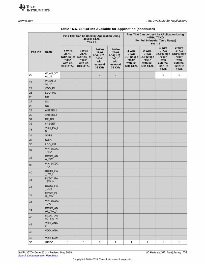
www.ti.com Pins Available for Applications
531SWRU367D–June 2014–Revised May 2018Submit Documentation Feedback
Copyright © 2014–2018, Texas Instruments Incorporated
I/O Pads and Pin Multiplexing
Table 16-6. GPIO/Pins Available for Application (continued)
Pkg Pin Name
Pins That Can be Used by Application Using40MHz XTAL
Yes = 1
Pins That Can be Used by APplication Using40MHz TCXO
(For Full Industrial Temp Range)Yes = 1
4-WireJTAG
SOP[2:0] ="000"
with 32-KHz XTAL
2-WireJTAG
SOP[2:0] ="001"
with 32-KHz XTAL
4-WireJTAG
SOP[2:0] ="000"with
external32 KHz
2-WireJTAG
SOP[2:0] ="001"with
external32 KHz
4-WireJTAG
SOP[2:0] ="000"
with 32-KHz XTAL
2-WireJTAG
SOP[2:0] ="001"
with 32-KHz XTAL
4-WireJTAG
SOP[2:0] ="000"with
external32-KHzXTAL
2-WireJTAG
SOP[2:0] ="001"with
external32-KHzXTAL
22 WLAN_XTAL_N 0 0 1 1
23 WLAN_XTAL_P
24 VDD_PLL25 LDO_IN226 NC27 NC28 NC29 ANTSEL130 ANTSEL231 RF_BG32 nRESET
33 VDD_PA_IN
34 SOP135 SOP036 LDO_IN1
37 VIN_DCDC_ANA
38 DCDC_ANA_SW
39 VIN_DCDC_PA
40 DCDC_PA_SW_P
41 DCDC_PA_SW_N
42 DCDC_PA_OUT
43 DCDC_DIG_SW
44 VIN_DCDC_DIG
45 DCDC_ANA2_SW_P
46 DCDC_ANA2_SW_N
47 VDD_ANA2
48 VDD_ANA1
49 VDD_RAM50 GPIO0 1 1 1 1 1 1 1 1
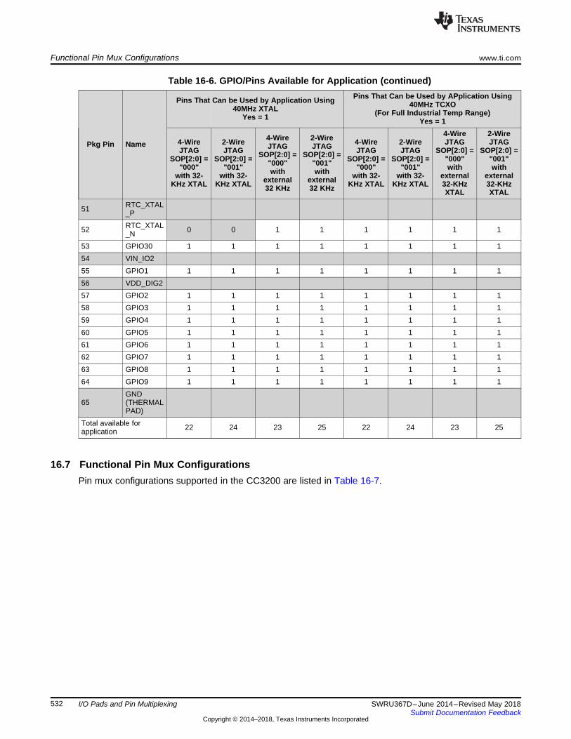
Functional Pin Mux Configurations www.ti.com
532 SWRU367D–June 2014–Revised May 2018Submit Documentation Feedback
Copyright © 2014–2018, Texas Instruments Incorporated
I/O Pads and Pin Multiplexing
Table 16-6. GPIO/Pins Available for Application (continued)
Pkg Pin Name
Pins That Can be Used by Application Using40MHz XTAL
Yes = 1
Pins That Can be Used by APplication Using40MHz TCXO
(For Full Industrial Temp Range)Yes = 1
4-WireJTAG
SOP[2:0] ="000"
with 32-KHz XTAL
2-WireJTAG
SOP[2:0] ="001"
with 32-KHz XTAL
4-WireJTAG
SOP[2:0] ="000"with
external32 KHz
2-WireJTAG
SOP[2:0] ="001"with
external32 KHz
4-WireJTAG
SOP[2:0] ="000"
with 32-KHz XTAL
2-WireJTAG
SOP[2:0] ="001"
with 32-KHz XTAL
4-WireJTAG
SOP[2:0] ="000"with
external32-KHzXTAL
2-WireJTAG
SOP[2:0] ="001"with
external32-KHzXTAL
51 RTC_XTAL_P
52 RTC_XTAL_N 0 0 1 1 1 1 1 1
53 GPIO30 1 1 1 1 1 1 1 154 VIN_IO255 GPIO1 1 1 1 1 1 1 1 156 VDD_DIG257 GPIO2 1 1 1 1 1 1 1 158 GPIO3 1 1 1 1 1 1 1 159 GPIO4 1 1 1 1 1 1 1 160 GPIO5 1 1 1 1 1 1 1 161 GPIO6 1 1 1 1 1 1 1 162 GPIO7 1 1 1 1 1 1 1 163 GPIO8 1 1 1 1 1 1 1 164 GPIO9 1 1 1 1 1 1 1 1
65GND(THERMALPAD)
Total available forapplication 22 24 23 25 22 24 23 25
16.7 Functional Pin Mux ConfigurationsPin mux configurations supported in the CC3200 are listed in Table 16-7.
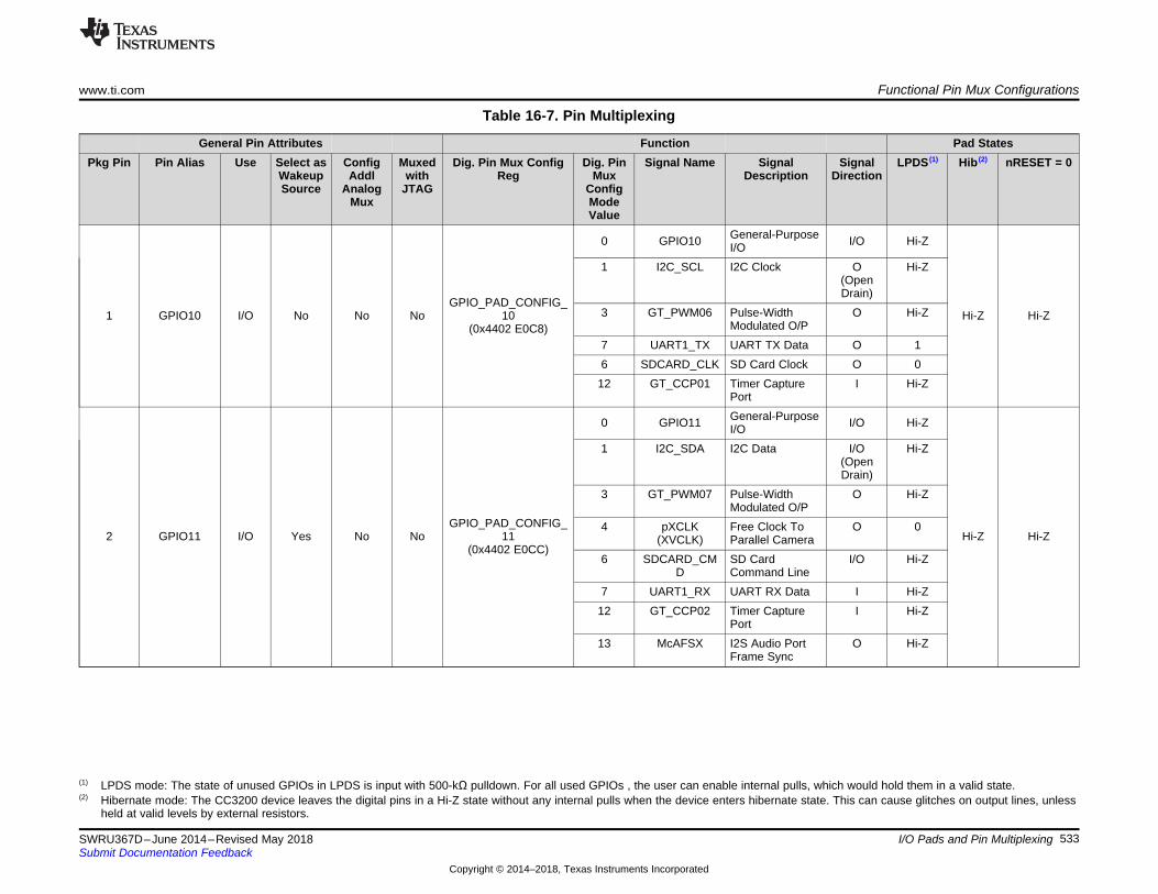
www.ti.com Functional Pin Mux Configurations
533SWRU367D–June 2014–Revised May 2018Submit Documentation Feedback
Copyright © 2014–2018, Texas Instruments Incorporated
I/O Pads and Pin Multiplexing
(1) LPDS mode: The state of unused GPIOs in LPDS is input with 500-kΩ pulldown. For all used GPIOs , the user can enable internal pulls, which would hold them in a valid state.(2) Hibernate mode: The CC3200 device leaves the digital pins in a Hi-Z state without any internal pulls when the device enters hibernate state. This can cause glitches on output lines, unless
held at valid levels by external resistors.
Table 16-7. Pin Multiplexing
General Pin Attributes Function Pad StatesPkg Pin Pin Alias Use Select as
WakeupSource
ConfigAddl
AnalogMux
Muxedwith
JTAG
Dig. Pin Mux ConfigReg
Dig. PinMux
ConfigModeValue
Signal Name SignalDescription
SignalDirection
LPDS (1) Hib (2) nRESET = 0
1 GPIO10 I/O No No NoGPIO_PAD_CONFIG_
10(0x4402 E0C8)
0 GPIO10 General-PurposeI/O I/O Hi-Z
Hi-Z Hi-Z
1 I2C_SCL I2C Clock O(OpenDrain)
Hi-Z
3 GT_PWM06 Pulse-WidthModulated O/P
O Hi-Z
7 UART1_TX UART TX Data O 16 SDCARD_CLK SD Card Clock O 0
12 GT_CCP01 Timer CapturePort
I Hi-Z
2 GPIO11 I/O Yes No NoGPIO_PAD_CONFIG_
11(0x4402 E0CC)
0 GPIO11 General-PurposeI/O I/O Hi-Z
Hi-Z Hi-Z
1 I2C_SDA I2C Data I/O(OpenDrain)
Hi-Z
3 GT_PWM07 Pulse-WidthModulated O/P
O Hi-Z
4 pXCLK(XVCLK)
Free Clock ToParallel Camera
O 0
6 SDCARD_CMD
SD CardCommand Line
I/O Hi-Z
7 UART1_RX UART RX Data I Hi-Z12 GT_CCP02 Timer Capture
PortI Hi-Z
13 McAFSX I2S Audio PortFrame Sync
O Hi-Z
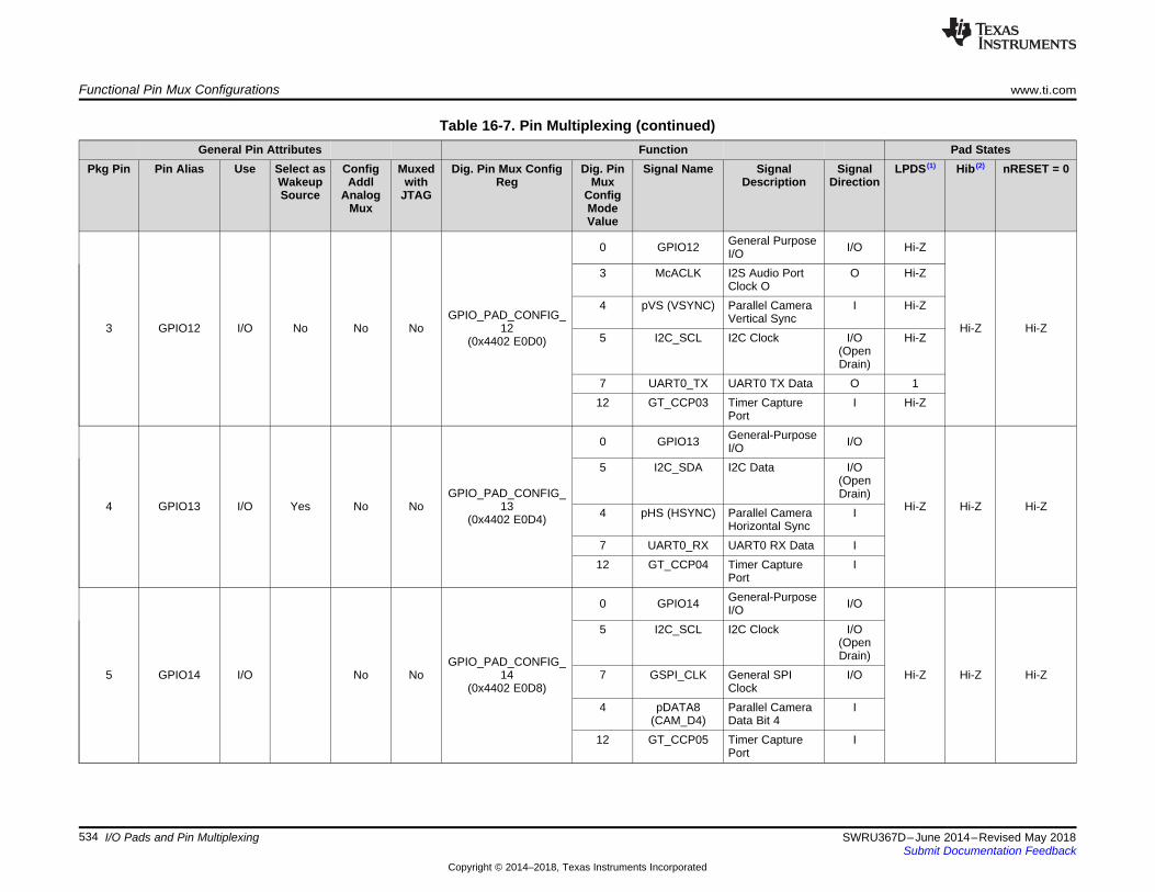
Functional Pin Mux Configurations www.ti.com
534 SWRU367D–June 2014–Revised May 2018Submit Documentation Feedback
Copyright © 2014–2018, Texas Instruments Incorporated
I/O Pads and Pin Multiplexing
Table 16-7. Pin Multiplexing (continued)General Pin Attributes Function Pad States
Pkg Pin Pin Alias Use Select asWakeupSource
ConfigAddl
AnalogMux
Muxedwith
JTAG
Dig. Pin Mux ConfigReg
Dig. PinMux
ConfigModeValue
Signal Name SignalDescription
SignalDirection
LPDS (1) Hib (2) nRESET = 0
3 GPIO12 I/O No No NoGPIO_PAD_CONFIG_
12(0x4402 E0D0)
0 GPIO12 General PurposeI/O I/O Hi-Z
Hi-Z Hi-Z
3 McACLK I2S Audio PortClock O
O Hi-Z
4 pVS (VSYNC) Parallel CameraVertical Sync
I Hi-Z
5 I2C_SCL I2C Clock I/O(OpenDrain)
Hi-Z
7 UART0_TX UART0 TX Data O 112 GT_CCP03 Timer Capture
PortI Hi-Z
4 GPIO13 I/O Yes No NoGPIO_PAD_CONFIG_
13(0x4402 E0D4)
0 GPIO13 General-PurposeI/O I/O
Hi-Z Hi-Z Hi-Z
5 I2C_SDA I2C Data I/O(OpenDrain)
4 pHS (HSYNC) Parallel CameraHorizontal Sync
I
7 UART0_RX UART0 RX Data I12 GT_CCP04 Timer Capture
PortI
5 GPIO14 I/O No NoGPIO_PAD_CONFIG_
14(0x4402 E0D8)
0 GPIO14 General-PurposeI/O I/O
Hi-Z Hi-Z Hi-Z
5 I2C_SCL I2C Clock I/O(OpenDrain)
7 GSPI_CLK General SPIClock
I/O
4 pDATA8(CAM_D4)
Parallel CameraData Bit 4
I
12 GT_CCP05 Timer CapturePort
I
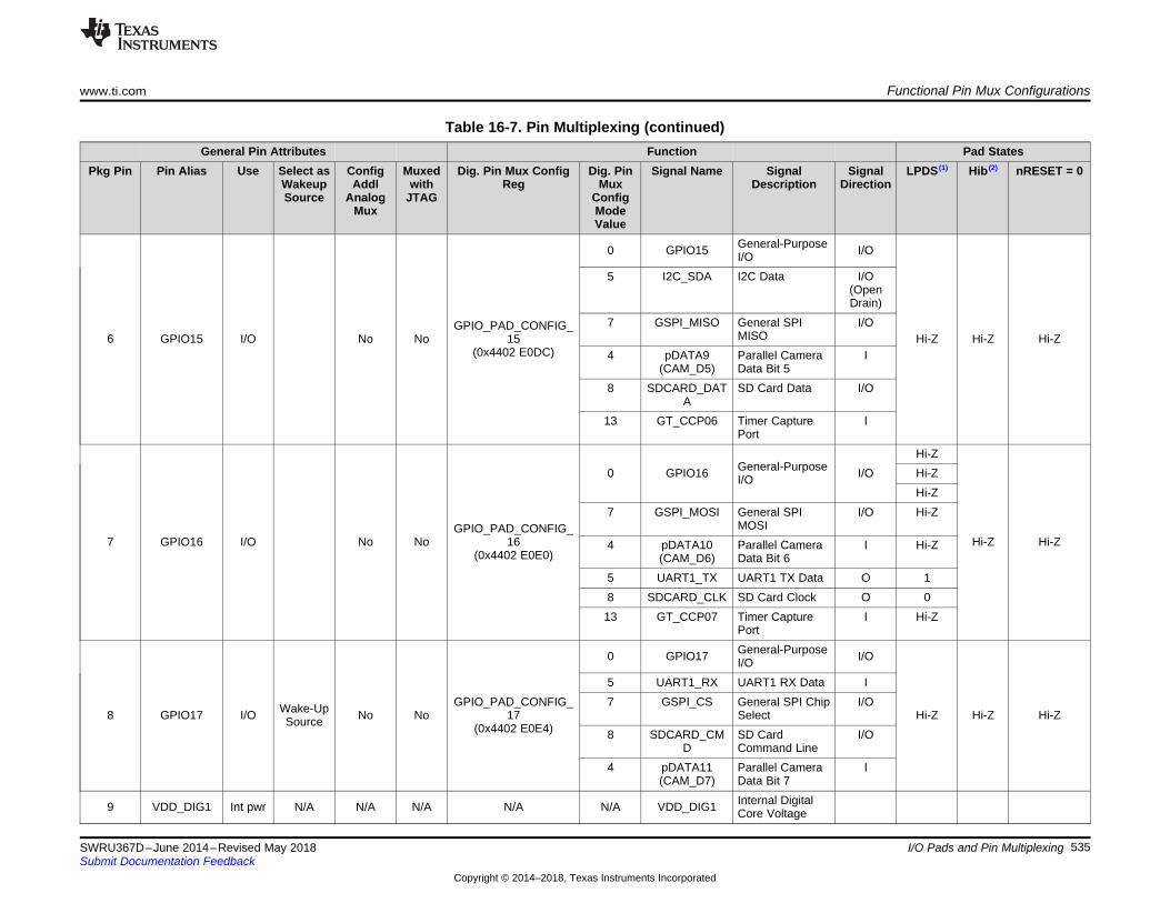
www.ti.com Functional Pin Mux Configurations
535SWRU367D–June 2014–Revised May 2018Submit Documentation Feedback
Copyright © 2014–2018, Texas Instruments Incorporated
I/O Pads and Pin Multiplexing
Table 16-7. Pin Multiplexing (continued)General Pin Attributes Function Pad States
Pkg Pin Pin Alias Use Select asWakeupSource
ConfigAddl
AnalogMux
Muxedwith
JTAG
Dig. Pin Mux ConfigReg
Dig. PinMux
ConfigModeValue
Signal Name SignalDescription
SignalDirection
LPDS (1) Hib (2) nRESET = 0
6 GPIO15 I/O No NoGPIO_PAD_CONFIG_
15(0x4402 E0DC)
0 GPIO15 General-PurposeI/O I/O
Hi-Z Hi-Z Hi-Z
5 I2C_SDA I2C Data I/O(OpenDrain)
7 GSPI_MISO General SPIMISO
I/O
4 pDATA9(CAM_D5)
Parallel CameraData Bit 5
I
8 SDCARD_DATA
SD Card Data I/O
13 GT_CCP06 Timer CapturePort
I
7 GPIO16 I/O No NoGPIO_PAD_CONFIG_
16(0x4402 E0E0)
0 GPIO16 General-PurposeI/O I/O
Hi-Z
Hi-Z Hi-Z
Hi-ZHi-Z
7 GSPI_MOSI General SPIMOSI
I/O Hi-Z
4 pDATA10(CAM_D6)
Parallel CameraData Bit 6
I Hi-Z
5 UART1_TX UART1 TX Data O 18 SDCARD_CLK SD Card Clock O 0
13 GT_CCP07 Timer CapturePort
I Hi-Z
8 GPIO17 I/O Wake-UpSource No No
GPIO_PAD_CONFIG_17
(0x4402 E0E4)
0 GPIO17 General-PurposeI/O I/O
Hi-Z Hi-Z Hi-Z
5 UART1_RX UART1 RX Data I7 GSPI_CS General SPI Chip
SelectI/O
8 SDCARD_CMD
SD CardCommand Line
I/O
4 pDATA11(CAM_D7)
Parallel CameraData Bit 7
I
9 VDD_DIG1 Int pwr N/A N/A N/A N/A N/A VDD_DIG1 Internal DigitalCore Voltage
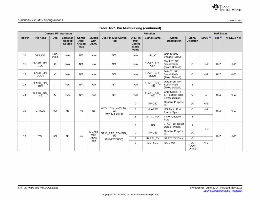
Functional Pin Mux Configurations www.ti.com
536 SWRU367D–June 2014–Revised May 2018Submit Documentation Feedback
Copyright © 2014–2018, Texas Instruments Incorporated
I/O Pads and Pin Multiplexing
Table 16-7. Pin Multiplexing (continued)General Pin Attributes Function Pad States
Pkg Pin Pin Alias Use Select asWakeupSource
ConfigAddl
AnalogMux
Muxedwith
JTAG
Dig. Pin Mux ConfigReg
Dig. PinMux
ConfigModeValue
Signal Name SignalDescription
SignalDirection
LPDS (1) Hib (2) nRESET = 0
10 VIN_IO1 Sup.input N/A N/A N/A N/A N/A VIN_IO1 Chip Supply
Voltage (VBAT)
11 FLASH_SPI_CLK O N/A N/A N/A N/A N/A FLASH_SPI_
CLK
Clock To SPISerial Flash(Fixed Default)
O Hi-Z Hi-Z Hi-Z
12 FLASH_SPI_DOUT O N/A N/A N/A N/A N/A FLASH_SPI_
DOUT
Data To SPISerial Flash(Fixed Default)
O Hi-Z Hi-Z Hi-Z
13 FLASH_SPI_DIN I N/A N/A N/A N/A N/A FLASH_SPI_
DIN
Data From SPISerial Flash(Fixed Default)
I
14 FLASH_SPI_CS O N/A N/A N/A N/A N/A FLASH_SPI_
CS
Chip Select ToSPI Serial Flash(Fixed Default)
O 1 Hi-Z Hi-Z
15 GPIO22 I/O No No NoGPIO_PAD_CONFIG_
22(0x4402 E0F8)
0 GPIO22 General-PurposeI/O I/O Hi-Z
Hi-Z Hi-Z7 McAFSX I2S Audio PortFrame Sync
O Hi-Z
5 GT_CCP04 Timer CapturePort
I
16 TDI I/O No No
MUXedwith
JTAGTDI
GPIO_PAD_CONFIG_23
(0x4402 E0FC)
1 TDI JTAG TDI. ResetDefault Pinout. I
Hi-Z
Hi-Z Hi-Z0 GPIO23 General-Purpose
I/O I/O
2 UART1_TX UART1 TX Data O 19 I2C_SCL I2C Clock I/O
(OpenDrain)
Hi-Z
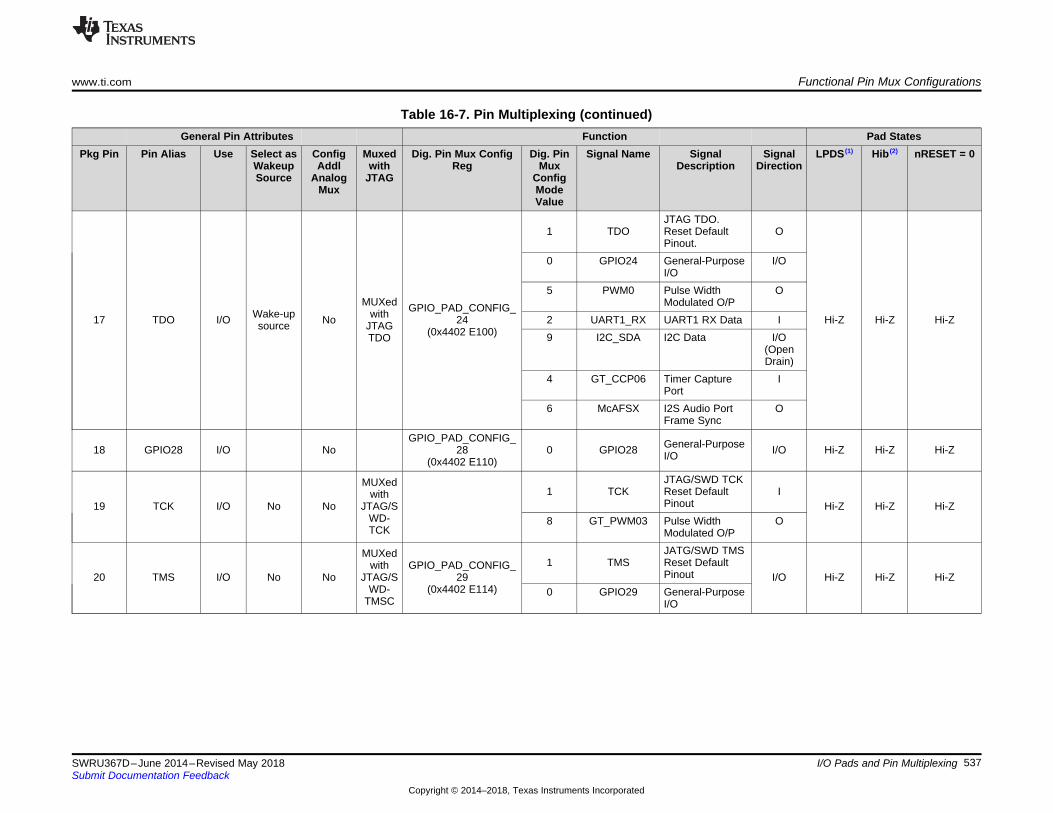
www.ti.com Functional Pin Mux Configurations
537SWRU367D–June 2014–Revised May 2018Submit Documentation Feedback
Copyright © 2014–2018, Texas Instruments Incorporated
I/O Pads and Pin Multiplexing
Table 16-7. Pin Multiplexing (continued)General Pin Attributes Function Pad States
Pkg Pin Pin Alias Use Select asWakeupSource
ConfigAddl
AnalogMux
Muxedwith
JTAG
Dig. Pin Mux ConfigReg
Dig. PinMux
ConfigModeValue
Signal Name SignalDescription
SignalDirection
LPDS (1) Hib (2) nRESET = 0
17 TDO I/O Wake-upsource No
MUXedwith
JTAGTDO
GPIO_PAD_CONFIG_24
(0x4402 E100)
1 TDOJTAG TDO.Reset DefaultPinout.
O
Hi-Z Hi-Z Hi-Z
0 GPIO24 General-PurposeI/O
I/O
5 PWM0 Pulse WidthModulated O/P
O
2 UART1_RX UART1 RX Data I9 I2C_SDA I2C Data I/O
(OpenDrain)
4 GT_CCP06 Timer CapturePort
I
6 McAFSX I2S Audio PortFrame Sync
O
18 GPIO28 I/O NoGPIO_PAD_CONFIG_
28(0x4402 E110)
0 GPIO28 General-PurposeI/O I/O Hi-Z Hi-Z Hi-Z
19 TCK I/O No No
MUXedwith
JTAG/SWD-TCK
1 TCKJTAG/SWD TCKReset DefaultPinout
IHi-Z Hi-Z Hi-Z
8 GT_PWM03 Pulse WidthModulated O/P
O
20 TMS I/O No No
MUXedwith
JTAG/SWD-
TMSC
GPIO_PAD_CONFIG_29
(0x4402 E114)
1 TMSJATG/SWD TMSReset DefaultPinout I/O Hi-Z Hi-Z Hi-Z
0 GPIO29 General-PurposeI/O
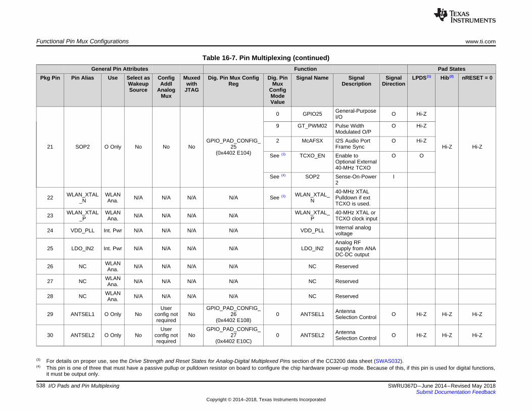
Functional Pin Mux Configurations www.ti.com
538 SWRU367D–June 2014–Revised May 2018Submit Documentation Feedback
Copyright © 2014–2018, Texas Instruments Incorporated
I/O Pads and Pin Multiplexing
Table 16-7. Pin Multiplexing (continued)General Pin Attributes Function Pad States
Pkg Pin Pin Alias Use Select asWakeupSource
ConfigAddl
AnalogMux
Muxedwith
JTAG
Dig. Pin Mux ConfigReg
Dig. PinMux
ConfigModeValue
Signal Name SignalDescription
SignalDirection
LPDS (1) Hib (2) nRESET = 0
(3) For details on proper use, see the Drive Strength and Reset States for Analog-Digital Multiplexed Pins section of the CC3200 data sheet (SWAS032).(4) This pin is one of three that must have a passive pullup or pulldown resistor on board to configure the chip hardware power-up mode. Because of this, if this pin is used for digital functions,
it must be output only.
21 SOP2 O Only No No NoGPIO_PAD_CONFIG_
25(0x4402 E104)
0 GPIO25 General-PurposeI/O O Hi-Z
Hi-Z Hi-Z
9 GT_PWM02 Pulse WidthModulated O/P
O Hi-Z
2 McAFSX I2S Audio PortFrame Sync
O Hi-Z
See (3) TCXO_EN Enable toOptional External40-MHz TCXO
O O
See (4) SOP2 Sense-On-Power2
I
22 WLAN_XTAL_N
WLANAna. N/A N/A N/A N/A See (3) WLAN_XTAL_
N
40-MHz XTALPulldown if extTCXO is used.
23 WLAN_XTAL_P
WLANAna. N/A N/A N/A N/A WLAN_XTAL_
P40-MHz XTAL orTCXO clock input
24 VDD_PLL Int. Pwr N/A N/A N/A N/A VDD_PLL Internal analogvoltage
25 LDO_IN2 Int. Pwr N/A N/A N/A N/A LDO_IN2Analog RFsupply from ANADC-DC output
26 NC WLANAna. N/A N/A N/A N/A NC Reserved
27 NC WLANAna. N/A N/A N/A N/A NC Reserved
28 NC WLANAna. N/A N/A N/A N/A NC Reserved
29 ANTSEL1 O Only NoUser
config notrequired
NoGPIO_PAD_CONFIG_
26(0x4402 E108)
0 ANTSEL1 AntennaSelection Control O Hi-Z Hi-Z Hi-Z
30 ANTSEL2 O Only NoUser
config notrequired
NoGPIO_PAD_CONFIG_
27(0x4402 E10C)
0 ANTSEL2 AntennaSelection Control O Hi-Z Hi-Z Hi-Z
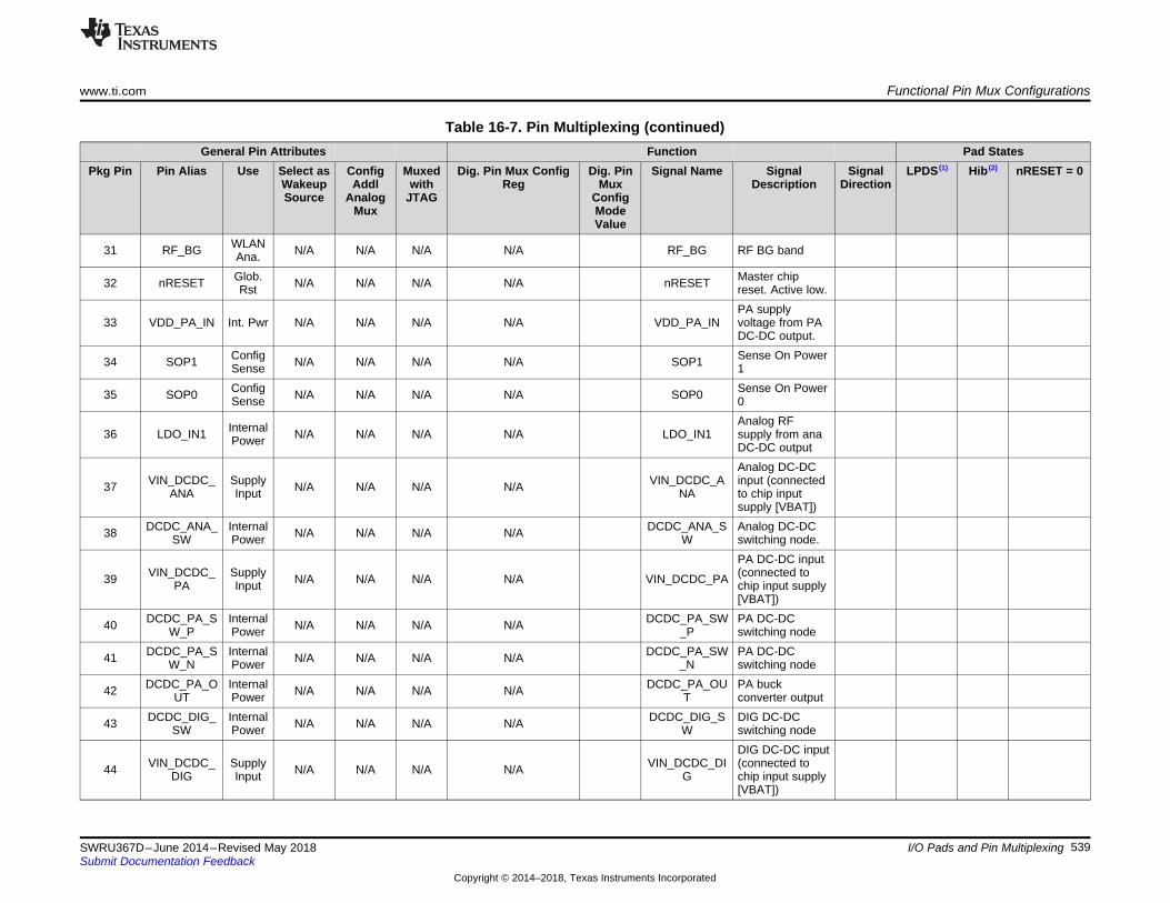
www.ti.com Functional Pin Mux Configurations
539SWRU367D–June 2014–Revised May 2018Submit Documentation Feedback
Copyright © 2014–2018, Texas Instruments Incorporated
I/O Pads and Pin Multiplexing
Table 16-7. Pin Multiplexing (continued)General Pin Attributes Function Pad States
Pkg Pin Pin Alias Use Select asWakeupSource
ConfigAddl
AnalogMux
Muxedwith
JTAG
Dig. Pin Mux ConfigReg
Dig. PinMux
ConfigModeValue
Signal Name SignalDescription
SignalDirection
LPDS (1) Hib (2) nRESET = 0
31 RF_BG WLANAna. N/A N/A N/A N/A RF_BG RF BG band
32 nRESET Glob.Rst N/A N/A N/A N/A nRESET Master chip
reset. Active low.
33 VDD_PA_IN Int. Pwr N/A N/A N/A N/A VDD_PA_INPA supplyvoltage from PADC-DC output.
34 SOP1 ConfigSense N/A N/A N/A N/A SOP1 Sense On Power
1
35 SOP0 ConfigSense N/A N/A N/A N/A SOP0 Sense On Power
0
36 LDO_IN1 InternalPower N/A N/A N/A N/A LDO_IN1
Analog RFsupply from anaDC-DC output
37 VIN_DCDC_ANA
SupplyInput N/A N/A N/A N/A VIN_DCDC_A
NA
Analog DC-DCinput (connectedto chip inputsupply [VBAT])
38 DCDC_ANA_SW
InternalPower N/A N/A N/A N/A DCDC_ANA_S
WAnalog DC-DCswitching node.
39 VIN_DCDC_PA
SupplyInput N/A N/A N/A N/A VIN_DCDC_PA
PA DC-DC input(connected tochip input supply[VBAT])
40 DCDC_PA_SW_P
InternalPower N/A N/A N/A N/A DCDC_PA_SW
_PPA DC-DCswitching node
41 DCDC_PA_SW_N
InternalPower N/A N/A N/A N/A DCDC_PA_SW
_NPA DC-DCswitching node
42 DCDC_PA_OUT
InternalPower N/A N/A N/A N/A DCDC_PA_OU
TPA buckconverter output
43 DCDC_DIG_SW
InternalPower N/A N/A N/A N/A DCDC_DIG_S
WDIG DC-DCswitching node
44 VIN_DCDC_DIG
SupplyInput N/A N/A N/A N/A VIN_DCDC_DI
G
DIG DC-DC input(connected tochip input supply[VBAT])
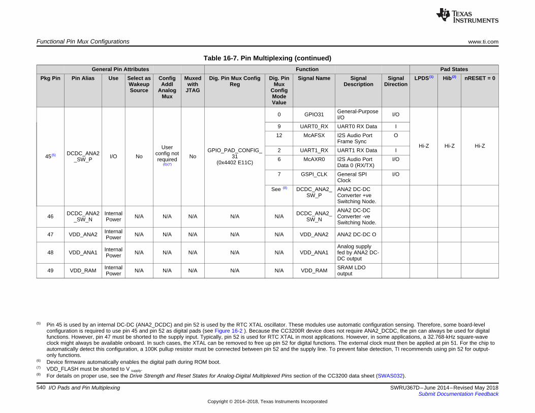
Functional Pin Mux Configurations www.ti.com
540 SWRU367D–June 2014–Revised May 2018Submit Documentation Feedback
Copyright © 2014–2018, Texas Instruments Incorporated
I/O Pads and Pin Multiplexing
Table 16-7. Pin Multiplexing (continued)General Pin Attributes Function Pad States
Pkg Pin Pin Alias Use Select asWakeupSource
ConfigAddl
AnalogMux
Muxedwith
JTAG
Dig. Pin Mux ConfigReg
Dig. PinMux
ConfigModeValue
Signal Name SignalDescription
SignalDirection
LPDS (1) Hib (2) nRESET = 0
(5) Pin 45 is used by an internal DC-DC (ANA2_DCDC) and pin 52 is used by the RTC XTAL oscillator. These modules use automatic configuration sensing. Therefore, some board-levelconfiguration is required to use pin 45 and pin 52 as digital pads (see Figure 16-2 ). Because the CC3200R device does not require ANA2_DCDC, the pin can always be used for digitalfunctions. However, pin 47 must be shorted to the supply input. Typically, pin 52 is used for RTC XTAL in most applications. However, in some applications, a 32.768-kHz square-waveclock might always be available onboard. In such cases, the XTAL can be removed to free up pin 52 for digital functions. The external clock must then be applied at pin 51. For the chip toautomatically detect this configuration, a 100K pullup resistor must be connected between pin 52 and the supply line. To prevent false detection, TI recommends using pin 52 for output-only functions.
(6) Device firmware automatically enables the digital path during ROM boot.(7) VDD_FLASH must be shorted to V supply.(8) For details on proper use, see the Drive Strength and Reset States for Analog-Digital Multiplexed Pins section of the CC3200 data sheet (SWAS032).
45 (5) DCDC_ANA2_SW_P I/O No
Userconfig notrequired
(6) (7)
NoGPIO_PAD_CONFIG_
31(0x4402 E11C)
0 GPIO31 General-PurposeI/O I/O
Hi-Z Hi-Z Hi-Z
9 UART0_RX UART0 RX Data I12 McAFSX I2S Audio Port
Frame SyncO
2 UART1_RX UART1 RX Data I6 McAXR0 I2S Audio Port
Data 0 (RX/TX)I/O
7 GSPI_CLK General SPIClock
I/O
See (8) DCDC_ANA2_SW_P
ANA2 DC-DCConverter +veSwitching Node.
46 DCDC_ANA2_SW_N
InternalPower N/A N/A N/A N/A N/A DCDC_ANA2_
SW_N
ANA2 DC-DCConverter -veSwitching Node.
47 VDD_ANA2 InternalPower N/A N/A N/A N/A N/A VDD_ANA2 ANA2 DC-DC O
48 VDD_ANA1 InternalPower N/A N/A N/A N/A N/A VDD_ANA1
Analog supplyfed by ANA2 DC-DC output
49 VDD_RAM InternalPower N/A N/A N/A N/A N/A VDD_RAM SRAM LDO
output
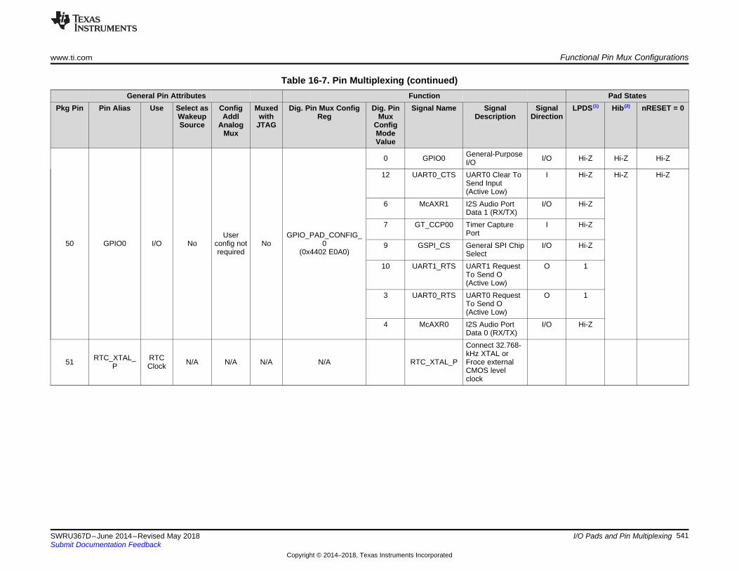
www.ti.com Functional Pin Mux Configurations
541SWRU367D–June 2014–Revised May 2018Submit Documentation Feedback
Copyright © 2014–2018, Texas Instruments Incorporated
I/O Pads and Pin Multiplexing
Table 16-7. Pin Multiplexing (continued)General Pin Attributes Function Pad States
Pkg Pin Pin Alias Use Select asWakeupSource
ConfigAddl
AnalogMux
Muxedwith
JTAG
Dig. Pin Mux ConfigReg
Dig. PinMux
ConfigModeValue
Signal Name SignalDescription
SignalDirection
LPDS (1) Hib (2) nRESET = 0
50 GPIO0 I/O NoUser
config notrequired
NoGPIO_PAD_CONFIG_
0(0x4402 E0A0)
0 GPIO0 General-PurposeI/O I/O Hi-Z Hi-Z Hi-Z
12 UART0_CTS UART0 Clear ToSend Input(Active Low)
I Hi-Z Hi-Z Hi-Z
6 McAXR1 I2S Audio PortData 1 (RX/TX)
I/O Hi-Z
7 GT_CCP00 Timer CapturePort
I Hi-Z
9 GSPI_CS General SPI ChipSelect
I/O Hi-Z
10 UART1_RTS UART1 RequestTo Send O(Active Low)
O 1
3 UART0_RTS UART0 RequestTo Send O(Active Low)
O 1
4 McAXR0 I2S Audio PortData 0 (RX/TX)
I/O Hi-Z
51 RTC_XTAL_P
RTCClock N/A N/A N/A N/A RTC_XTAL_P
Connect 32.768-kHz XTAL orFroce externalCMOS levelclock
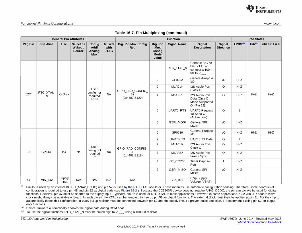
Functional Pin Mux Configurations www.ti.com
542 SWRU367D–June 2014–Revised May 2018Submit Documentation Feedback
Copyright © 2014–2018, Texas Instruments Incorporated
I/O Pads and Pin Multiplexing
Table 16-7. Pin Multiplexing (continued)General Pin Attributes Function Pad States
Pkg Pin Pin Alias Use Select asWakeupSource
ConfigAddl
AnalogMux
Muxedwith
JTAG
Dig. Pin Mux ConfigReg
Dig. PinMux
ConfigModeValue
Signal Name SignalDescription
SignalDirection
LPDS (1) Hib (2) nRESET = 0
(9) Pin 45 is used by an internal DC-DC (ANA2_DCDC) and pin 52 is used by the RTC XTAL oscillator. These modules use automatic configuration sensing. Therefore, some board-levelconfiguration is required to use pin 45 and pin 52 as digital pads (see Figure 16-2 ). Because the CC3200R device does not require ANA2_DCDC, the pin can always be used for digitalfunctions. However, pin 47 must be shorted to the supply input. Typically, pin 52 is used for RTC XTAL in most applications. However, in some applications, a 32.768-kHz square-waveclock might always be available onboard. In such cases, the XTAL can be removed to free up pin 52 for digital functions. The external clock must then be applied at pin 51. For the chip toautomatically detect this configuration, a 100K pullup resistor must be connected between pin 52 and the supply line. To prevent false detection, TI recommends using pin 52 for output-only functions.
(10) Device firmware automatically enables the digital path during ROM boot.(11) To use the digital functions, RTC_XTAL_N must be pulled high to V supply using a 100-KΩ resistor
52 (9) RTC_XTAL_N O Only
Userconfig notrequired
(10) (11)
NoGPIO_PAD_CONFIG_
32(0x4402 E120)
RTC_XTAL_N
Connect 32.768-kHz XTAL orconnect a 100-kΩ to Vsupply.
Hi-Z Hi-Z
0 GPIO32 General-PurposeI/O I/O Hi-Z
2 McACLK I2S Audio PortClock O
O Hi-Z
4 McAXR0 I2S Audio PortData (Only OMode SupportedOn Pin 52)
O Hi-Z
6 UART0_RTS UART0 RequestTo Send O(Active Low)
O 1
8 GSPI_MOSI General SPIMOSI
I/O Hi-Z
53 GPIO30 I/O No
Userconfig notrequired
(10)
NoGPIO_PAD_CONFIG_
30(0x4402 E118)
0 GPIO30 General-PurposeI/O I/O Hi-Z Hi-Z Hi-Z
9 UART0_TX UART0 TX Data O 12 McACLK I2S Audio Port
Clock OO Hi-Z
3 McAFSX I2S Audio PortFrame Sync
O Hi-Z
4 GT_CCP05 Timer CapturePort
I Hi-Z
7 GSPI_MISO General SPIMISO
I/O Hi-Z
54 VIN_IO2 SupplyInput N/A N/A N/A N/A VIN_IO2 Chip Supply
Voltage (VBAT)
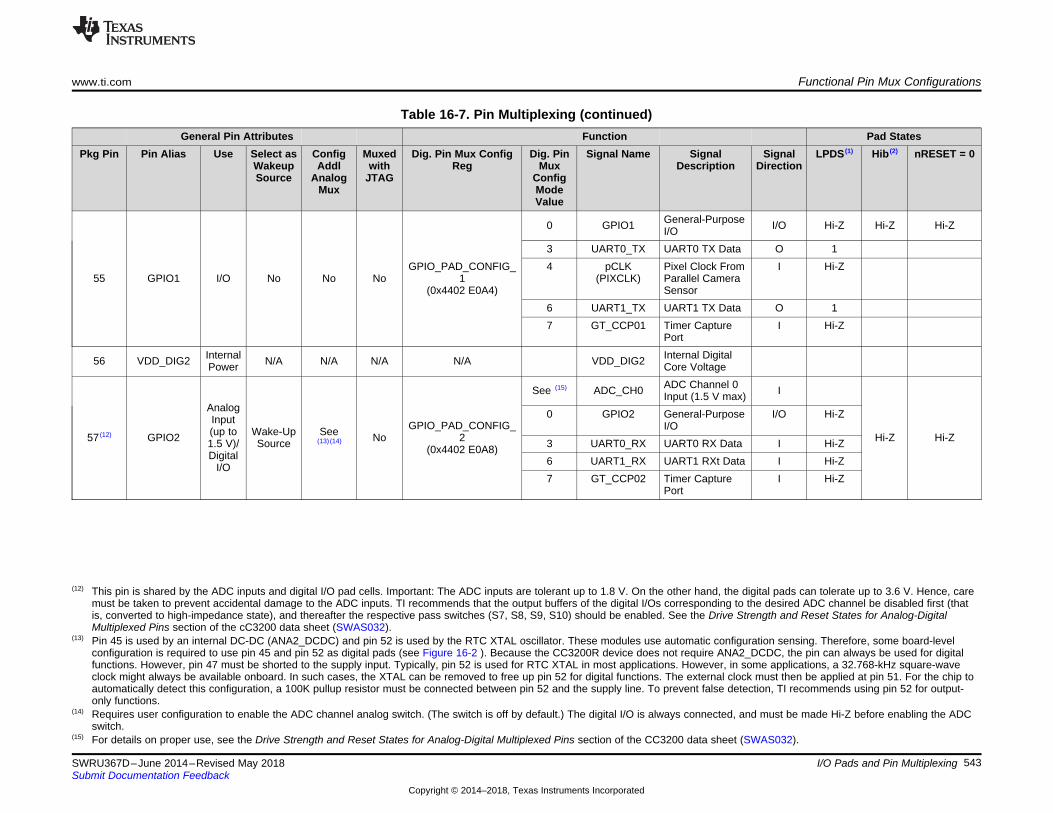
www.ti.com Functional Pin Mux Configurations
543SWRU367D–June 2014–Revised May 2018Submit Documentation Feedback
Copyright © 2014–2018, Texas Instruments Incorporated
I/O Pads and Pin Multiplexing
Table 16-7. Pin Multiplexing (continued)General Pin Attributes Function Pad States
Pkg Pin Pin Alias Use Select asWakeupSource
ConfigAddl
AnalogMux
Muxedwith
JTAG
Dig. Pin Mux ConfigReg
Dig. PinMux
ConfigModeValue
Signal Name SignalDescription
SignalDirection
LPDS (1) Hib (2) nRESET = 0
(12) This pin is shared by the ADC inputs and digital I/O pad cells. Important: The ADC inputs are tolerant up to 1.8 V. On the other hand, the digital pads can tolerate up to 3.6 V. Hence, caremust be taken to prevent accidental damage to the ADC inputs. TI recommends that the output buffers of the digital I/Os corresponding to the desired ADC channel be disabled first (thatis, converted to high-impedance state), and thereafter the respective pass switches (S7, S8, S9, S10) should be enabled. See the Drive Strength and Reset States for Analog-DigitalMultiplexed Pins section of the cC3200 data sheet (SWAS032).
(13) Pin 45 is used by an internal DC-DC (ANA2_DCDC) and pin 52 is used by the RTC XTAL oscillator. These modules use automatic configuration sensing. Therefore, some board-levelconfiguration is required to use pin 45 and pin 52 as digital pads (see Figure 16-2 ). Because the CC3200R device does not require ANA2_DCDC, the pin can always be used for digitalfunctions. However, pin 47 must be shorted to the supply input. Typically, pin 52 is used for RTC XTAL in most applications. However, in some applications, a 32.768-kHz square-waveclock might always be available onboard. In such cases, the XTAL can be removed to free up pin 52 for digital functions. The external clock must then be applied at pin 51. For the chip toautomatically detect this configuration, a 100K pullup resistor must be connected between pin 52 and the supply line. To prevent false detection, TI recommends using pin 52 for output-only functions.
(14) Requires user configuration to enable the ADC channel analog switch. (The switch is off by default.) The digital I/O is always connected, and must be made Hi-Z before enabling the ADCswitch.
(15) For details on proper use, see the Drive Strength and Reset States for Analog-Digital Multiplexed Pins section of the CC3200 data sheet (SWAS032).
55 GPIO1 I/O No No NoGPIO_PAD_CONFIG_
1(0x4402 E0A4)
0 GPIO1 General-PurposeI/O I/O Hi-Z Hi-Z Hi-Z
3 UART0_TX UART0 TX Data O 14 pCLK
(PIXCLK)Pixel Clock FromParallel CameraSensor
I Hi-Z
6 UART1_TX UART1 TX Data O 17 GT_CCP01 Timer Capture
PortI Hi-Z
56 VDD_DIG2 InternalPower N/A N/A N/A N/A VDD_DIG2 Internal Digital
Core Voltage
57 (12) GPIO2
AnalogInput(up to1.5 V)/Digital
I/O
Wake-UpSource
See(13) (14) No
GPIO_PAD_CONFIG_2
(0x4402 E0A8)
See (15) ADC_CH0 ADC Channel 0Input (1.5 V max) I
Hi-Z Hi-Z
0 GPIO2 General-PurposeI/O
I/O Hi-Z
3 UART0_RX UART0 RX Data I Hi-Z6 UART1_RX UART1 RXt Data I Hi-Z7 GT_CCP02 Timer Capture
PortI Hi-Z
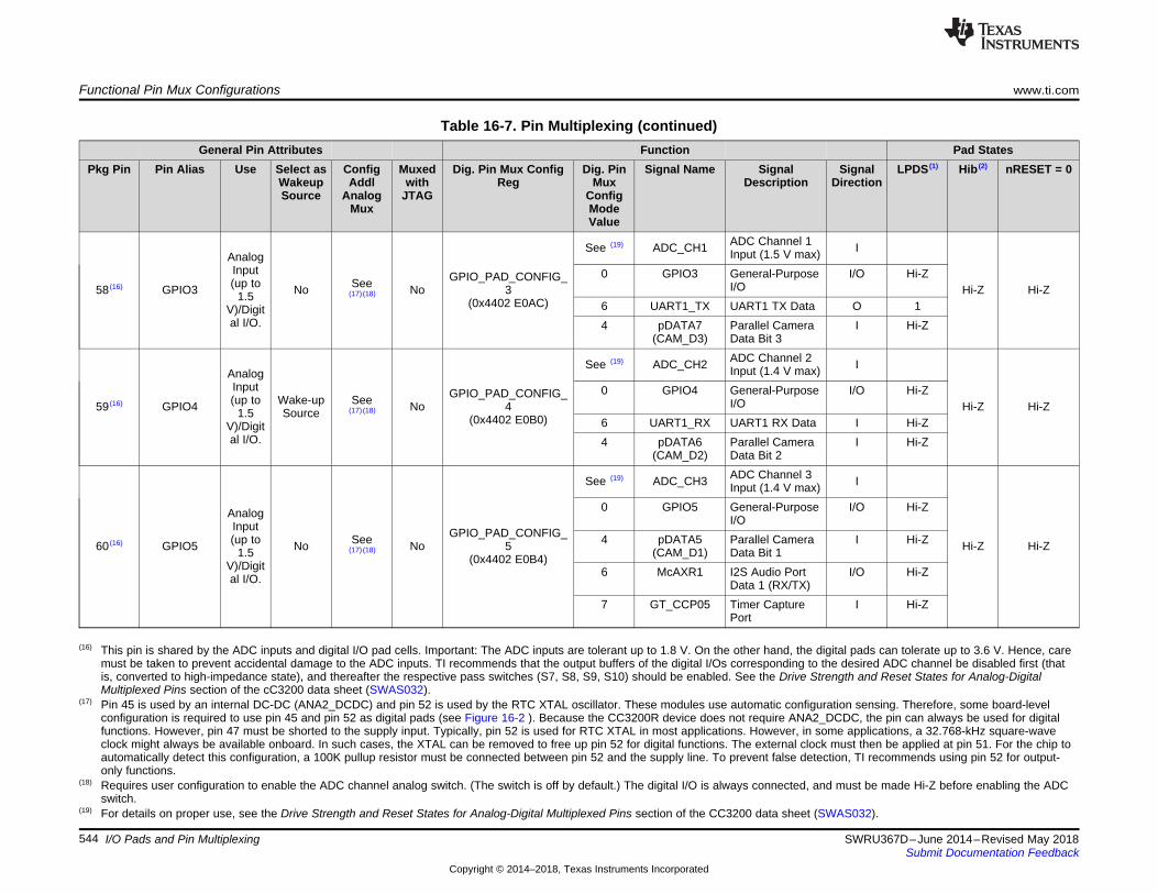
Functional Pin Mux Configurations www.ti.com
544 SWRU367D–June 2014–Revised May 2018Submit Documentation Feedback
Copyright © 2014–2018, Texas Instruments Incorporated
I/O Pads and Pin Multiplexing
Table 16-7. Pin Multiplexing (continued)General Pin Attributes Function Pad States
Pkg Pin Pin Alias Use Select asWakeupSource
ConfigAddl
AnalogMux
Muxedwith
JTAG
Dig. Pin Mux ConfigReg
Dig. PinMux
ConfigModeValue
Signal Name SignalDescription
SignalDirection
LPDS (1) Hib (2) nRESET = 0
(16) This pin is shared by the ADC inputs and digital I/O pad cells. Important: The ADC inputs are tolerant up to 1.8 V. On the other hand, the digital pads can tolerate up to 3.6 V. Hence, caremust be taken to prevent accidental damage to the ADC inputs. TI recommends that the output buffers of the digital I/Os corresponding to the desired ADC channel be disabled first (thatis, converted to high-impedance state), and thereafter the respective pass switches (S7, S8, S9, S10) should be enabled. See the Drive Strength and Reset States for Analog-DigitalMultiplexed Pins section of the cC3200 data sheet (SWAS032).
(17) Pin 45 is used by an internal DC-DC (ANA2_DCDC) and pin 52 is used by the RTC XTAL oscillator. These modules use automatic configuration sensing. Therefore, some board-levelconfiguration is required to use pin 45 and pin 52 as digital pads (see Figure 16-2 ). Because the CC3200R device does not require ANA2_DCDC, the pin can always be used for digitalfunctions. However, pin 47 must be shorted to the supply input. Typically, pin 52 is used for RTC XTAL in most applications. However, in some applications, a 32.768-kHz square-waveclock might always be available onboard. In such cases, the XTAL can be removed to free up pin 52 for digital functions. The external clock must then be applied at pin 51. For the chip toautomatically detect this configuration, a 100K pullup resistor must be connected between pin 52 and the supply line. To prevent false detection, TI recommends using pin 52 for output-only functions.
(18) Requires user configuration to enable the ADC channel analog switch. (The switch is off by default.) The digital I/O is always connected, and must be made Hi-Z before enabling the ADCswitch.
(19) For details on proper use, see the Drive Strength and Reset States for Analog-Digital Multiplexed Pins section of the CC3200 data sheet (SWAS032).
58 (16) GPIO3
AnalogInput(up to
1.5V)/Digital I/O.
No See(17) (18) No
GPIO_PAD_CONFIG_3
(0x4402 E0AC)
See (19) ADC_CH1 ADC Channel 1Input (1.5 V max) I
Hi-Z Hi-Z0 GPIO3 General-Purpose
I/OI/O Hi-Z
6 UART1_TX UART1 TX Data O 14 pDATA7
(CAM_D3)Parallel CameraData Bit 3
I Hi-Z
59 (16) GPIO4
AnalogInput(up to
1.5V)/Digital I/O.
Wake-upSource
See(17) (18) No
GPIO_PAD_CONFIG_4
(0x4402 E0B0)
See (19) ADC_CH2 ADC Channel 2Input (1.4 V max) I
Hi-Z Hi-Z0 GPIO4 General-Purpose
I/OI/O Hi-Z
6 UART1_RX UART1 RX Data I Hi-Z4 pDATA6
(CAM_D2)Parallel CameraData Bit 2
I Hi-Z
60 (16) GPIO5
AnalogInput(up to
1.5V)/Digital I/O.
No See(17) (18) No
GPIO_PAD_CONFIG_5
(0x4402 E0B4)
See (19) ADC_CH3 ADC Channel 3Input (1.4 V max) I
Hi-Z Hi-Z
0 GPIO5 General-PurposeI/O
I/O Hi-Z
4 pDATA5(CAM_D1)
Parallel CameraData Bit 1
I Hi-Z
6 McAXR1 I2S Audio PortData 1 (RX/TX)
I/O Hi-Z
7 GT_CCP05 Timer CapturePort
I Hi-Z
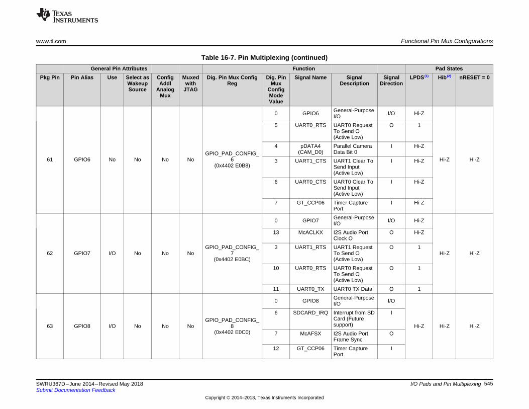
www.ti.com Functional Pin Mux Configurations
545SWRU367D–June 2014–Revised May 2018Submit Documentation Feedback
Copyright © 2014–2018, Texas Instruments Incorporated
I/O Pads and Pin Multiplexing
Table 16-7. Pin Multiplexing (continued)General Pin Attributes Function Pad States
Pkg Pin Pin Alias Use Select asWakeupSource
ConfigAddl
AnalogMux
Muxedwith
JTAG
Dig. Pin Mux ConfigReg
Dig. PinMux
ConfigModeValue
Signal Name SignalDescription
SignalDirection
LPDS (1) Hib (2) nRESET = 0
61 GPIO6 No No No NoGPIO_PAD_CONFIG_
6(0x4402 E0B8)
0 GPIO6 General-PurposeI/O I/O Hi-Z
Hi-Z Hi-Z
5 UART0_RTS UART0 RequestTo Send O(Active Low)
O 1
4 pDATA4(CAM_D0)
Parallel CameraData Bit 0
I Hi-Z
3 UART1_CTS UART1 Clear ToSend Input(Active Low)
I Hi-Z
6 UART0_CTS UART0 Clear ToSend Input(Active Low)
I Hi-Z
7 GT_CCP06 Timer CapturePort
I Hi-Z
62 GPIO7 I/O No No NoGPIO_PAD_CONFIG_
7(0x4402 E0BC)
0 GPIO7 General-PurposeI/O I/O Hi-Z
Hi-Z Hi-Z
13 McACLKX I2S Audio PortClock O
O Hi-Z
3 UART1_RTS UART1 RequestTo Send O(Active Low)
O 1
10 UART0_RTS UART0 RequestTo Send O(Active Low)
O 1
11 UART0_TX UART0 TX Data O 1
63 GPIO8 I/O No No NoGPIO_PAD_CONFIG_
8(0x4402 E0C0)
0 GPIO8 General-PurposeI/O I/O
Hi-Z Hi-Z Hi-Z
6 SDCARD_IRQ Interrupt from SDCard (Futuresupport)
I
7 McAFSX I2S Audio PortFrame Sync
O
12 GT_CCP06 Timer CapturePort
I
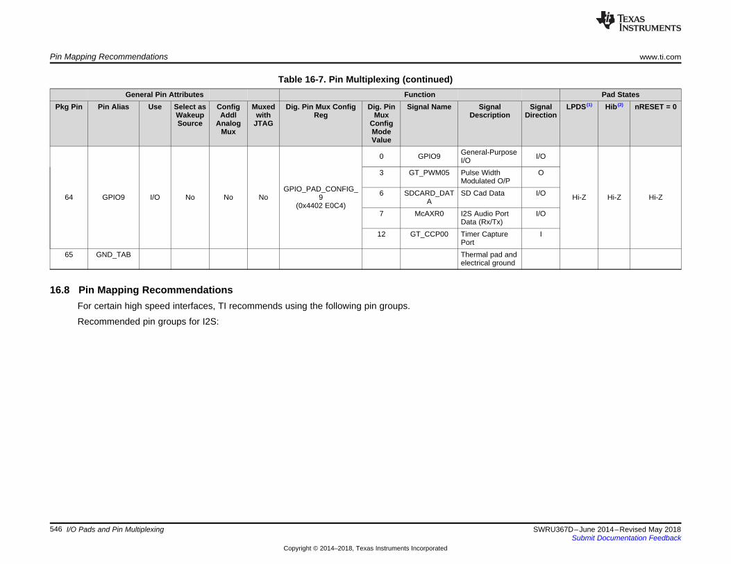
Pin Mapping Recommendations www.ti.com
546 SWRU367D–June 2014–Revised May 2018Submit Documentation Feedback
Copyright © 2014–2018, Texas Instruments Incorporated
I/O Pads and Pin Multiplexing
Table 16-7. Pin Multiplexing (continued)General Pin Attributes Function Pad States
Pkg Pin Pin Alias Use Select asWakeupSource
ConfigAddl
AnalogMux
Muxedwith
JTAG
Dig. Pin Mux ConfigReg
Dig. PinMux
ConfigModeValue
Signal Name SignalDescription
SignalDirection
LPDS (1) Hib (2) nRESET = 0
64 GPIO9 I/O No No NoGPIO_PAD_CONFIG_
9(0x4402 E0C4)
0 GPIO9 General-PurposeI/O I/O
Hi-Z Hi-Z Hi-Z
3 GT_PWM05 Pulse WidthModulated O/P
O
6 SDCARD_DATA
SD Cad Data I/O
7 McAXR0 I2S Audio PortData (Rx/Tx)
I/O
12 GT_CCP00 Timer CapturePort
I
65 GND_TAB Thermal pad andelectrical ground
16.8 Pin Mapping RecommendationsFor certain high speed interfaces, TI recommends using the following pin groups.
Recommended pin groups for I2S:
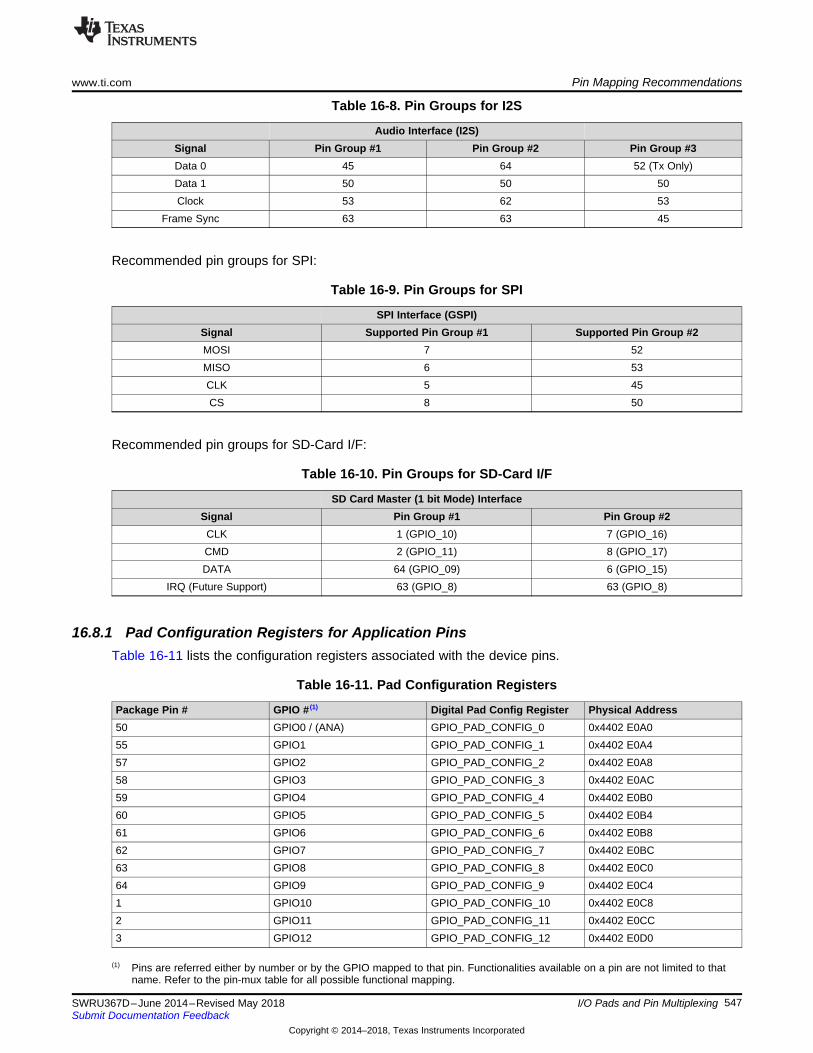
www.ti.com Pin Mapping Recommendations
547SWRU367D–June 2014–Revised May 2018Submit Documentation Feedback
Copyright © 2014–2018, Texas Instruments Incorporated
I/O Pads and Pin Multiplexing
Table 16-8. Pin Groups for I2S
Audio Interface (I2S)Signal Pin Group #1 Pin Group #2 Pin Group #3Data 0 45 64 52 (Tx Only)Data 1 50 50 50Clock 53 62 53
Frame Sync 63 63 45
Recommended pin groups for SPI:
Table 16-9. Pin Groups for SPI
SPI Interface (GSPI)Signal Supported Pin Group #1 Supported Pin Group #2MOSI 7 52MISO 6 53CLK 5 45CS 8 50
Recommended pin groups for SD-Card I/F:
Table 16-10. Pin Groups for SD-Card I/F
SD Card Master (1 bit Mode) InterfaceSignal Pin Group #1 Pin Group #2CLK 1 (GPIO_10) 7 (GPIO_16)CMD 2 (GPIO_11) 8 (GPIO_17)DATA 64 (GPIO_09) 6 (GPIO_15)
IRQ (Future Support) 63 (GPIO_8) 63 (GPIO_8)
16.8.1 Pad Configuration Registers for Application PinsTable 16-11 lists the configuration registers associated with the device pins.
(1) Pins are referred either by number or by the GPIO mapped to that pin. Functionalities available on a pin are not limited to thatname. Refer to the pin-mux table for all possible functional mapping.
Table 16-11. Pad Configuration Registers
Package Pin # GPIO # (1) Digital Pad Config Register Physical Address50 GPIO0 / (ANA) GPIO_PAD_CONFIG_0 0x4402 E0A055 GPIO1 GPIO_PAD_CONFIG_1 0x4402 E0A457 GPIO2 GPIO_PAD_CONFIG_2 0x4402 E0A858 GPIO3 GPIO_PAD_CONFIG_3 0x4402 E0AC59 GPIO4 GPIO_PAD_CONFIG_4 0x4402 E0B060 GPIO5 GPIO_PAD_CONFIG_5 0x4402 E0B461 GPIO6 GPIO_PAD_CONFIG_6 0x4402 E0B862 GPIO7 GPIO_PAD_CONFIG_7 0x4402 E0BC63 GPIO8 GPIO_PAD_CONFIG_8 0x4402 E0C064 GPIO9 GPIO_PAD_CONFIG_9 0x4402 E0C41 GPIO10 GPIO_PAD_CONFIG_10 0x4402 E0C82 GPIO11 GPIO_PAD_CONFIG_11 0x4402 E0CC3 GPIO12 GPIO_PAD_CONFIG_12 0x4402 E0D0
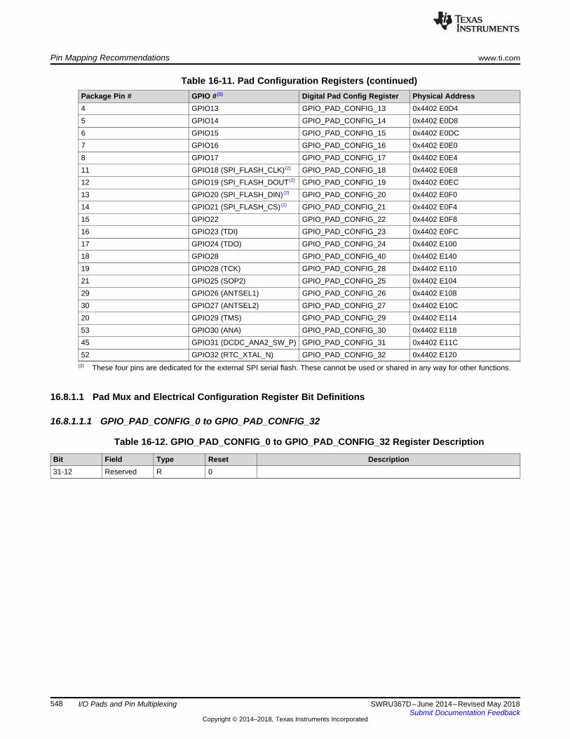
Pin Mapping Recommendations www.ti.com
548 SWRU367D–June 2014–Revised May 2018Submit Documentation Feedback
Copyright © 2014–2018, Texas Instruments Incorporated
I/O Pads and Pin Multiplexing
Table 16-11. Pad Configuration Registers (continued)Package Pin # GPIO # (1) Digital Pad Config Register Physical Address
(2) These four pins are dedicated for the external SPI serial flash. These cannot be used or shared in any way for other functions.
4 GPIO13 GPIO_PAD_CONFIG_13 0x4402 E0D45 GPIO14 GPIO_PAD_CONFIG_14 0x4402 E0D86 GPIO15 GPIO_PAD_CONFIG_15 0x4402 E0DC7 GPIO16 GPIO_PAD_CONFIG_16 0x4402 E0E08 GPIO17 GPIO_PAD_CONFIG_17 0x4402 E0E411 GPIO18 (SPI_FLASH_CLK) (2) GPIO_PAD_CONFIG_18 0x4402 E0E812 GPIO19 (SPI_FLASH_DOUT (2) GPIO_PAD_CONFIG_19 0x4402 E0EC13 GPIO20 (SPI_FLASH_DIN) (2) GPIO_PAD_CONFIG_20 0x4402 E0F014 GPIO21 (SPI_FLASH_CS) (2) GPIO_PAD_CONFIG_21 0x4402 E0F415 GPIO22 GPIO_PAD_CONFIG_22 0x4402 E0F816 GPIO23 (TDI) GPIO_PAD_CONFIG_23 0x4402 E0FC17 GPIO24 (TDO) GPIO_PAD_CONFIG_24 0x4402 E10018 GPIO28 GPIO_PAD_CONFIG_40 0x4402 E14019 GPIO28 (TCK) GPIO_PAD_CONFIG_28 0x4402 E11021 GPIO25 (SOP2) GPIO_PAD_CONFIG_25 0x4402 E10429 GPIO26 (ANTSEL1) GPIO_PAD_CONFIG_26 0x4402 E10830 GPIO27 (ANTSEL2) GPIO_PAD_CONFIG_27 0x4402 E10C20 GPIO29 (TMS) GPIO_PAD_CONFIG_29 0x4402 E11453 GPIO30 (ANA) GPIO_PAD_CONFIG_30 0x4402 E11845 GPIO31 (DCDC_ANA2_SW_P) GPIO_PAD_CONFIG_31 0x4402 E11C52 GPIO32 (RTC_XTAL_N) GPIO_PAD_CONFIG_32 0x4402 E120
16.8.1.1 Pad Mux and Electrical Configuration Register Bit Definitions
16.8.1.1.1 GPIO_PAD_CONFIG_0 to GPIO_PAD_CONFIG_32
Table 16-12. GPIO_PAD_CONFIG_0 to GPIO_PAD_CONFIG_32 Register Description
Bit Field Type Reset Description31-12 Reserved R 0
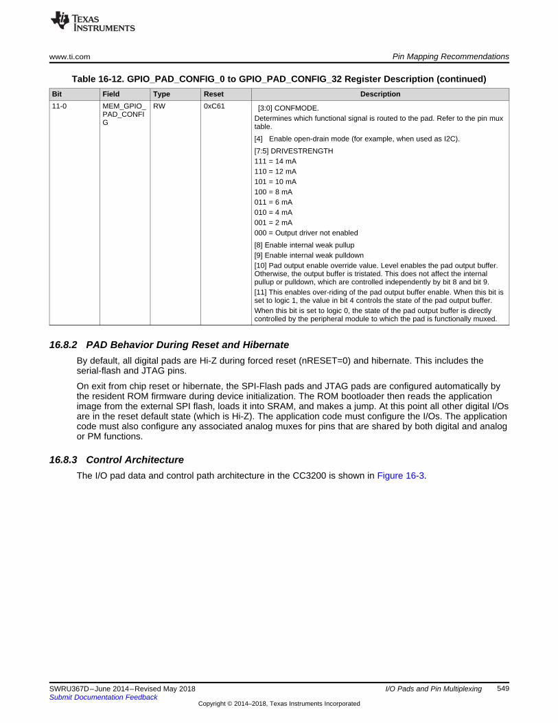
www.ti.com Pin Mapping Recommendations
549SWRU367D–June 2014–Revised May 2018Submit Documentation Feedback
Copyright © 2014–2018, Texas Instruments Incorporated
I/O Pads and Pin Multiplexing
Table 16-12. GPIO_PAD_CONFIG_0 to GPIO_PAD_CONFIG_32 Register Description (continued)Bit Field Type Reset Description11-0 MEM_GPIO_
PAD_CONFIG
RW 0xC61 [3:0] CONFMODE.Determines which functional signal is routed to the pad. Refer to the pin muxtable.
[4] Enable open-drain mode (for example, when used as I2C).
[7:5] DRIVESTRENGTH111 = 14 mA110 = 12 mA101 = 10 mA100 = 8 mA011 = 6 mA010 = 4 mA001 = 2 mA000 = Output driver not enabled
[8] Enable internal weak pullup[9] Enable internal weak pulldown[10] Pad output enable override value. Level enables the pad output buffer.Otherwise, the output buffer is tristated. This does not affect the internalpullup or pulldown, which are controlled independently by bit 8 and bit 9.[11] This enables over-riding of the pad output buffer enable. When this bit isset to logic 1, the value in bit 4 controls the state of the pad output buffer.When this bit is set to logic 0, the state of the pad output buffer is directlycontrolled by the peripheral module to which the pad is functionally muxed.
16.8.2 PAD Behavior During Reset and HibernateBy default, all digital pads are Hi-Z during forced reset (nRESET=0) and hibernate. This includes theserial-flash and JTAG pins.
On exit from chip reset or hibernate, the SPI-Flash pads and JTAG pads are configured automatically bythe resident ROM firmware during device initialization. The ROM bootloader then reads the applicationimage from the external SPI flash, loads it into SRAM, and makes a jump. At this point all other digital I/Osare in the reset default state (which is Hi-Z). The application code must configure the I/Os. The applicationcode must also configure any associated analog muxes for pins that are shared by both digital and analogor PM functions.
16.8.3 Control ArchitectureThe I/O pad data and control path architecture in the CC3200 is shown in Figure 16-3.
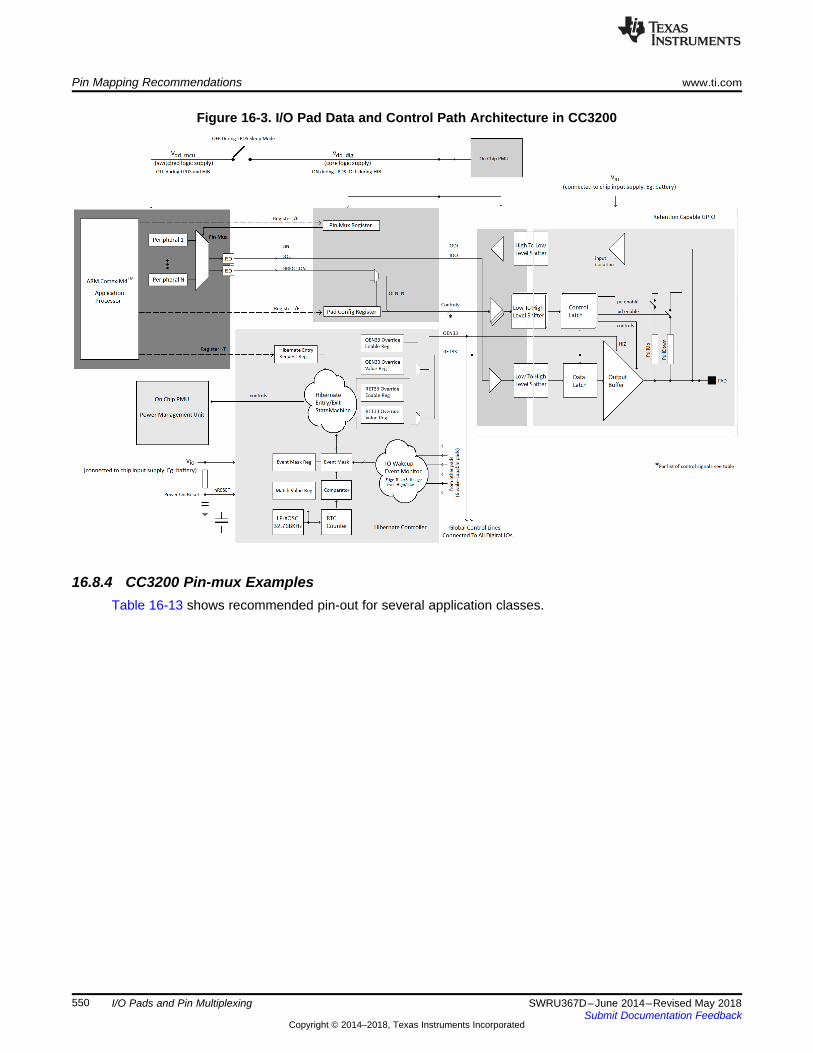
Pin Mapping Recommendations www.ti.com
550 SWRU367D–June 2014–Revised May 2018Submit Documentation Feedback
Copyright © 2014–2018, Texas Instruments Incorporated
I/O Pads and Pin Multiplexing
Figure 16-3. I/O Pad Data and Control Path Architecture in CC3200
16.8.4 CC3200 Pin-mux ExamplesTable 16-13 shows recommended pin-out for several application classes.
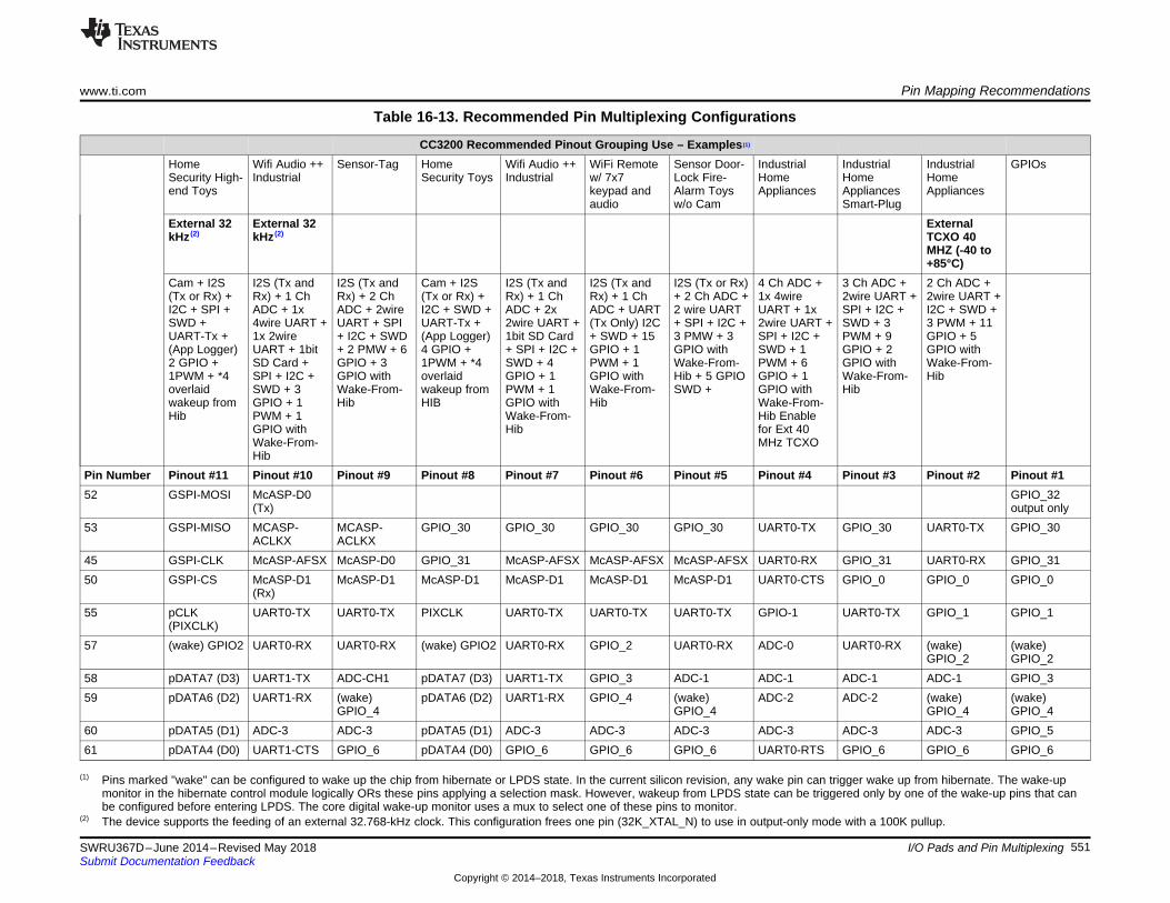
www.ti.com Pin Mapping Recommendations
551SWRU367D–June 2014–Revised May 2018Submit Documentation Feedback
Copyright © 2014–2018, Texas Instruments Incorporated
I/O Pads and Pin Multiplexing
(1) Pins marked "wake" can be configured to wake up the chip from hibernate or LPDS state. In the current silicon revision, any wake pin can trigger wake up from hibernate. The wake-upmonitor in the hibernate control module logically ORs these pins applying a selection mask. However, wakeup from LPDS state can be triggered only by one of the wake-up pins that canbe configured before entering LPDS. The core digital wake-up monitor uses a mux to select one of these pins to monitor.
(2) The device supports the feeding of an external 32.768-kHz clock. This configuration frees one pin (32K_XTAL_N) to use in output-only mode with a 100K pullup.
Table 16-13. Recommended Pin Multiplexing Configurations
CC3200 Recommended Pinout Grouping Use – Examples (1)
HomeSecurity High-end Toys
Wifi Audio ++Industrial
Sensor-Tag HomeSecurity Toys
Wifi Audio ++Industrial
WiFi Remotew/ 7x7keypad andaudio
Sensor Door-Lock Fire-Alarm Toysw/o Cam
IndustrialHomeAppliances
IndustrialHomeAppliancesSmart-Plug
IndustrialHomeAppliances
GPIOs
External 32kHz (2)
External 32kHz (2)
ExternalTCXO 40MHZ (-40 to+85°C)
Cam + I2S(Tx or Rx) +I2C + SPI +SWD +UART-Tx +(App Logger)2 GPIO +1PWM + *4overlaidwakeup fromHib
I2S (Tx andRx) + 1 ChADC + 1x4wire UART +1x 2wireUART + 1bitSD Card +SPI + I2C +SWD + 3GPIO + 1PWM + 1GPIO withWake-From-Hib
I2S (Tx andRx) + 2 ChADC + 2wireUART + SPI+ I2C + SWD+ 2 PMW + 6GPIO + 3GPIO withWake-From-Hib
Cam + I2S(Tx or Rx) +I2C + SWD +UART-Tx +(App Logger)4 GPIO +1PWM + *4overlaidwakeup fromHIB
I2S (Tx andRx) + 1 ChADC + 2x2wire UART +1bit SD Card+ SPI + I2C +SWD + 4GPIO + 1PWM + 1GPIO withWake-From-Hib
I2S (Tx andRx) + 1 ChADC + UART(Tx Only) I2C+ SWD + 15GPIO + 1PWM + 1GPIO withWake-From-Hib
I2S (Tx or Rx)+ 2 Ch ADC +2 wire UART+ SPI + I2C +3 PMW + 3GPIO withWake-From-Hib + 5 GPIOSWD +
4 Ch ADC +1x 4wireUART + 1x2wire UART +SPI + I2C +SWD + 1PWM + 6GPIO + 1GPIO withWake-From-Hib Enablefor Ext 40MHz TCXO
3 Ch ADC +2wire UART +SPI + I2C +SWD + 3PWM + 9GPIO + 2GPIO withWake-From-Hib
2 Ch ADC +2wire UART +I2C + SWD +3 PWM + 11GPIO + 5GPIO withWake-From-Hib
Pin Number Pinout #11 Pinout #10 Pinout #9 Pinout #8 Pinout #7 Pinout #6 Pinout #5 Pinout #4 Pinout #3 Pinout #2 Pinout #152 GSPI-MOSI McASP-D0
(Tx)GPIO_32output only
53 GSPI-MISO MCASP-ACLKX
MCASP-ACLKX
GPIO_30 GPIO_30 GPIO_30 GPIO_30 UART0-TX GPIO_30 UART0-TX GPIO_30
45 GSPI-CLK McASP-AFSX McASP-D0 GPIO_31 McASP-AFSX McASP-AFSX McASP-AFSX UART0-RX GPIO_31 UART0-RX GPIO_3150 GSPI-CS McASP-D1
(Rx)McASP-D1 McASP-D1 McASP-D1 McASP-D1 McASP-D1 UART0-CTS GPIO_0 GPIO_0 GPIO_0
55 pCLK(PIXCLK)
UART0-TX UART0-TX PIXCLK UART0-TX UART0-TX UART0-TX GPIO-1 UART0-TX GPIO_1 GPIO_1
57 (wake) GPIO2 UART0-RX UART0-RX (wake) GPIO2 UART0-RX GPIO_2 UART0-RX ADC-0 UART0-RX (wake)GPIO_2
(wake)GPIO_2
58 pDATA7 (D3) UART1-TX ADC-CH1 pDATA7 (D3) UART1-TX GPIO_3 ADC-1 ADC-1 ADC-1 ADC-1 GPIO_359 pDATA6 (D2) UART1-RX (wake)
GPIO_4pDATA6 (D2) UART1-RX GPIO_4 (wake)
GPIO_4ADC-2 ADC-2 (wake)
GPIO_4(wake)GPIO_4
60 pDATA5 (D1) ADC-3 ADC-3 pDATA5 (D1) ADC-3 ADC-3 ADC-3 ADC-3 ADC-3 ADC-3 GPIO_561 pDATA4 (D0) UART1-CTS GPIO_6 pDATA4 (D0) GPIO_6 GPIO_6 GPIO_6 UART0-RTS GPIO_6 GPIO_6 GPIO_6
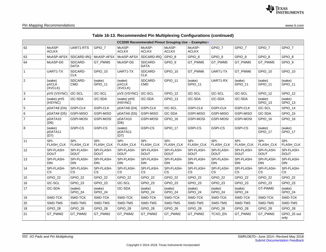
Pin Mapping Recommendations www.ti.com
552 SWRU367D–June 2014–Revised May 2018Submit Documentation Feedback
Copyright © 2014–2018, Texas Instruments Incorporated
I/O Pads and Pin Multiplexing
Table 16-13. Recommended Pin Multiplexing Configurations (continued)CC3200 Recommended Pinout Grouping Use – Examples (1)
62 McASP-ACLKX
UART1-RTS GPIO_7 McASP-ACLKX
McASP-ACLKX
McASP-ACLKX
McASP-ACLKX
GPIO_7 GPIO_7 GPIO_7 GPIO_7
63 McASP-AFSX SDCARD-IRQ McASP-AFSX McASP-AFSX SDCARD-IRQ GPIO_8 GPIO_8 GPIO_8 GPIO_8 GPIO_8 GPIO_864 McASP-D0 SDCARD-
DATAGT_PWM5 McASP-D0 SDCARD-
DATAGPIO_9 GT_PWM5 GT_PWM5 GT_PWM5 GT_PWM5 GPIO_9
1 UART1-TX SDCARD-CLK
GPIO_10 UART1-TX SDCARD-CLK
GPIO_10 GT_PWM6 UART1-TX GT_PWM6 GPIO_10 GPIO_10
2 (wake)pXCLK(XVCLK)
SDCARD-CMD
(wake)GPIO_11
(wake)pXCLK(XVCLK)
SDCARD-CMD
GPIO_11 (wake)GPIO_11
UART1-RX (wake)GPIO_11
(wake)GPIO_11
(wake)GPIO_11
3 pVS (VSYNC) I2C-SCL I2C-SCL pVS (VSYNC) I2C-SCL GPIO_12 I2C-SCL I2C-SCL I2C-SCL GPIO_12 GPIO_124 (wake) pHS
(HSYNC)I2C-SDA I2C-SDA (wake) pHS
(HSYNC)I2C-SDA GPIO_13 I2C-SDA I2C-SDA I2C-SDA (wake)
GPIO_13(wake)GPIO_13
5 pDATA8 (D4) GSPI-CLK GSPI-CLK pDATA8 (D4) GSPI-CLK I2C-SCL GSPI-CLK GSPI-CLK GSPI-CLK I2C-SCL GPIO_146 pDATA9 (D5) GSPI-MISO GSPI-MISO pDATA9 (D5) GSPI-MISO I2C-SDA GSPI-MISO GSPI-MISO GSPI-MISO I2C-SDA GPIO_157 pDATA10
(D6)GSPI-MOSI GSPI-MOSI pDATA10
(D6)GSPI-MOSI GPIO_16 GSPI-MOSI GSPI-MOSI GSPI-MOSI GPIO_16 GPIO_16
8 (wake)pDATA11(D7)
GSPI-CS GSPI-CS (wake)pDATA11(D7)
GSPI-CS GPIO_17 GSPI-CS GSPI-CS GSPI-CS (wake)GPIO_17
(wake)GPIO_17
11 SPI-FLASH_CLK
SPI-FLASH_CLK
SPI-FLASH_CLK
SPI-FLASH_CLK
SPI-FLASH_CLK
SPI-FLASH_CLK
SPI-FLASH_CLK
SPI-FLASH_CLK
SPI-FLASH_CLK
SPI-FLASH_CLK
SPI-FLASH_CLK
12 SPI-FLASH-DOUT
SPI-FLASH-DOUT
SPI-FLASH-DOUT
SPI-FLASH-DOUT
SPI-FLASH-DOUT
SPI-FLASH-DOUT
SPI-FLASH-DOUT
SPI-FLASH-DOUT
SPI-FLASH-DOUT
SPI-FLASH-DOUT
SPI-FLASH-DOUT
13 SPI-FLASH-DIN
SPI-FLASH-DIN
SPI-FLASH-DIN
SPI-FLASH-DIN
SPI-FLASH-DIN
SPI-FLASH-DIN
SPI-FLASH-DIN
SPI-FLASH-DIN
SPI-FLASH-DIN
SPI-FLASH-DIN
SPI-FLASH-DIN
14 SPI-FLASH-CS
SPI-FLASH-CS
SPI-FLASH-CS
SPI-FLASH-CS
SPI-FLASH-CS
SPI-FLASH-CS
SPI-FLASH-CS
SPI-FLASH-CS
SPI-FLASH-CS
SPI-FLASH-CS
SPI-FLASH-CS
15 GPIO_22 GPIO_22 GPIO_22 GPIO_22 GPIO_22 GPIO_22 GPIO_22 GPIO_22 GPIO_22 GPIO_22 GPIO_2216 I2C-SCL GPIO_23 GPIO_23 I2C-SCL GPIO_23 GPIO_23 GPIO_23 GPIO_23 GPIO_23 GPIO_23 GPIO_2317 I2C-SDA (wake)
GPIO_24(wake)GPIO_24
I2C-SDA (wake)GPIO_24
(wake)GPIO_24
(wake)GPIO_24
(wake)GPIO_24
(wake)GPIO_24
GT-PWM0 (wake)GPIO_24
19 SWD-TCK SWD-TCK SWD-TCK SWD-TCK SWD-TCK SWD-TCK SWD-TCK SWD-TCK SWD-TCK SWD-TCK SWD-TCK20 SWD-TMS SWD-TMS SWD-TMS SWD-TMS SWD-TMS SWD-TMS SWD-TMS SWD-TMS SWD-TMS SWD-TMS SWD-TMS18 GPIO_28 GPIO_28 GPIO_28 GPIO_28 GPIO_28 GPIO_28 GPIO_28 GPIO_28 GPIO_28 GPIO_28 GPIO_2821 GT_PWM2 GT_PWM2 GT_PWM2 GT_PWM2 GT_PWM2 GT_PWM2 GT_PWM2 TCXO_EN GT_PWM2 GT_PWM2 GPIO_25 out
only
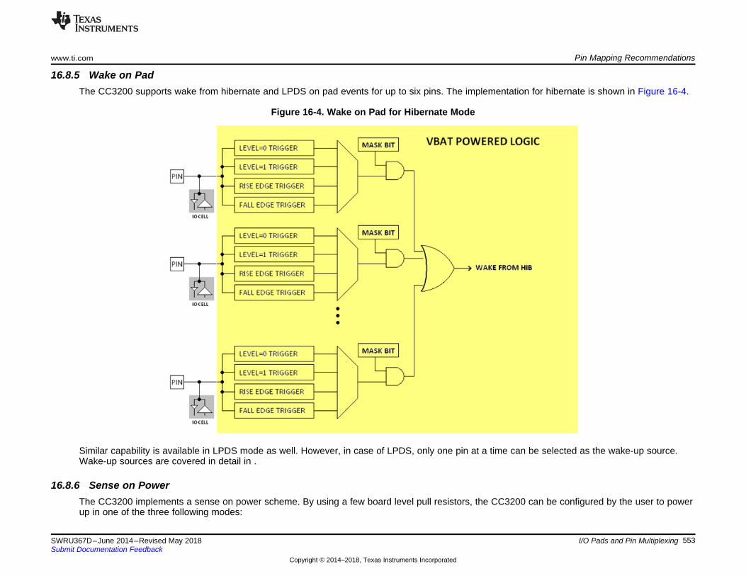
www.ti.com Pin Mapping Recommendations
553SWRU367D–June 2014–Revised May 2018Submit Documentation Feedback
Copyright © 2014–2018, Texas Instruments Incorporated
I/O Pads and Pin Multiplexing
16.8.5 Wake on PadThe CC3200 supports wake from hibernate and LPDS on pad events for up to six pins. The implementation for hibernate is shown in Figure 16-4.
Figure 16-4. Wake on Pad for Hibernate Mode
Similar capability is available in LPDS mode as well. However, in case of LPDS, only one pin at a time can be selected as the wake-up source.Wake-up sources are covered in detail in .
16.8.6 Sense on PowerThe CC3200 implements a sense on power scheme. By using a few board level pull resistors, the CC3200 can be configured by the user to powerup in one of the three following modes:
Pin Mapping Recommendations www.ti.com
554 SWRU367D–June 2014–Revised May 2018Submit Documentation Feedback
Copyright © 2014–2018, Texas Instruments Incorporated
I/O Pads and Pin Multiplexing
1. Fn4WJ: Functional mode with 4-wire JTAG mapped to fixed pins2. Fn2WJ: Functional mode with 2-wire SWD mapped to fixed pins3. LDfrUART : UART load mode for flashing the system during development and in OEM assembly line (for example: serial flash connected to
CC3200R)
Sense-on-power (SoP) values are sensed from the device pin during power up. This encoding determines the boot flow, as well as the defaultmapping for some of the pins (JTAG, SWD, UART0). Three SoP pins are used for this purpose. Before the device is taken out of reset, the SoPvalues are made available on a register and determine the device character while powering up. Table 16-14 shows the pull configurations.
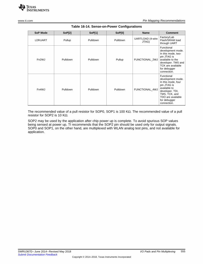
www.ti.com Pin Mapping Recommendations
555SWRU367D–June 2014–Revised May 2018Submit Documentation Feedback
Copyright © 2014–2018, Texas Instruments Incorporated
I/O Pads and Pin Multiplexing
Table 16-14. Sense-on-Power Configurations
SoP Mode SoP[2] SoP[1] SoP[0] Name Comment
LDfrUART Pullup Pulldown Pulldown UARTLOAD (4-wireJTAG)
Factory/LabFlash/SRAM loadthrough UART
Fn2WJ Pulldown Pulldown Pullup FUNCTIONAL_2WJ
Functionaldevelopment mode.In this mode, two-pin JTAG isavailable to thedeveloper. TMS andTCK are availablefor debuggerconnection.
Fn4WJ Pulldown Pulldown Pulldown FUNCTIONAL_4WJ
Functionaldevelopment mode.In this mode, fourpin JTAG isavailable todeveloper. TDI,TMS, TCK, andTDO are availablefor debuggerconnection.
The recommended value of a pull resistor for SOP0, SOP1 is 100 KΩ. The recommended value of a pullresistor for SOP2 is 10 KΩ.
SOP2 may be used by the application after chip power up is complete. To avoid spurious SOP valuesbeing sensed at power up, TI recommends that the SOP2 pin should be used only for output signals.SOP0 and SOP1, on the other hand, are multiplexed with WLAN analog test pins, and not available forapplication.
556 SWRU367D–June 2014–Revised May 2018Submit Documentation Feedback
Copyright © 2014–2018, Texas Instruments Incorporated
Software Development Kit Examples
Appendix ASWRU367D–June 2014–Revised May 2018
Software Development Kit Examples
A.1 Software Development Kit ExamplesThe CC3200 SDK kit contains several examples of sample code for most of the peripherals covered in thisdocument. Table A-1 provides links to examples for each of the peripherals. Also refer to the CC3200SDK Sample Applications wiki page.
Table A-1. Peripheral Samples
Peripheral Chapter Sample Examples with URLs
DMA Chapter 4 1. uDMA Application2. UART DMA Application
GPIO Chapter 5 1. Blinky Application2. Timer Demo Application
UART Chapter 6 1. UART Demo Application2. UART DMA Application
I2C Chapter 7 1. I2C ApplicationSPI Chapter 8 1. SPI Reference ApplicationGPT Chapter 9 1. PWM ApplicationWDT Chapter 10 1. Watchdog Demo Application
SD Host Chapter 11 1. SDHost Application2. SDHost FatFS Application
I2S Chapter 12 1. Wi-Fi Audio ApplicationADC Chapter 13 1. ADC Reference
Parallel camera interface Chapter 14 1. Camera Application
557SWRU367D–June 2014–Revised May 2018Submit Documentation Feedback
Copyright © 2014–2018, Texas Instruments Incorporated
CC3200 Miscellaneous Registers
Appendix BSWRU367D–June 2014–Revised May 2018
CC3200 Miscellaneous Registers
This chapter lists miscellaneous registers which do not belong to any one module, but hold informationcorresponding to multiple modules and peripherals.
B.1 Miscellaneous Register SummaryTable B-1 lists the memory-mapped registers for the REGISTER_SUMMARY. All register offset addressesnot listed in Table B-1 should be considered as reserved locations and the register contents should not bemodified.
Table B-1. Miscellaneous Register Summary
Offset Acronym Register Name Section8Ch DMA_IMR DMA_IMR Register Section B.1.190h DMA_IMS DMA_IMS Register Section B.1.294h DMA_IMC DMA_IMC Register Section B.1.39Ch DMA_ICR DMA_ICR Register Section B.1.4A0h DMA_MIS DMA_MIS Register Section B.1.5A4h DMA_RIS DMA_RIS Register Section B.1.6B0h GPTTRIGSEL GPTTRIGSEL Register Section B.1.7
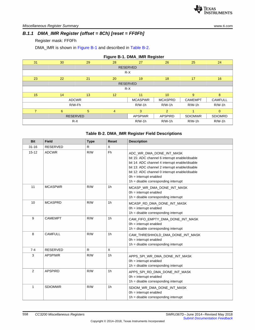
Miscellaneous Register Summary www.ti.com
558 SWRU367D–June 2014–Revised May 2018Submit Documentation Feedback
Copyright © 2014–2018, Texas Instruments Incorporated
CC3200 Miscellaneous Registers
B.1.1 DMA_IMR Register (offset = 8Ch) [reset = FF0Fh]Register mask: FF0Fh
DMA_IMR is shown in Figure B-1 and described in Table B-2.
Figure B-1. DMA_IMR Register31 30 29 28 27 26 25 24
RESERVEDR-X
23 22 21 20 19 18 17 16RESERVED
R-X
15 14 13 12 11 10 9 8ADCWR MCASPWR MCASPRD CAMEMPT CAMFULLR/W-Fh R/W-1h R/W-1h R/W-1h R/W-1h
7 6 5 4 3 2 1 0RESERVED APSPIWR APSPIRD SDIOMWR SDIOMRD
R-X R/W-1h R/W-1h R/W-1h R/W-1h
Table B-2. DMA_IMR Register Field Descriptions
Bit Field Type Reset Description31-16 RESERVED R X15-12 ADCWR R/W Fh ADC_WR_DMA_DONE_INT_MASK
bit 15: ADC channel 6 interrupt enable/disablebit 14: ADC channel 4 interrupt enable/disablebit 13: ADC channel 2 interrupt enable/disablebit 12: ADC channel 0 interrupt enable/disable0h = interrupt enabled1h = disable corresponding interrupt
11 MCASPWR R/W 1h MCASP_WR_DMA_DONE_INT_MASK0h = interrupt enabled1h = disable corresponding interrupt
10 MCASPRD R/W 1h MCASP_RD_DMA_DONE_INT_MASK0h = interrupt enabled1h = disable corresponding interrupt
9 CAMEMPT R/W 1h CAM_FIFO_EMPTY_DMA_DONE_INT_MASK0h = interrupt enabled1h = disable corresponding interrupt
8 CAMFULL R/W 1h CAM_THRESHHOLD_DMA_DONE_INT_MASK0h = interrupt enabled1h = disable corresponding interrupt
7-4 RESERVED R X3 APSPIWR R/W 1h APPS_SPI_WR_DMA_DONE_INT_MASK
0h = interrupt enabled1h = disable corresponding interrupt
2 APSPIRD R/W 1h APPS_SPI_RD_DMA_DONE_INT_MASK0h = interrupt enabled1h = disable corresponding interrupt
1 SDIOMWR R/W 1h SDIOM_WR_DMA_DONE_INT_MASK0h = interrupt enabled1h = disable corresponding interrupt
www.ti.com Miscellaneous Register Summary
559SWRU367D–June 2014–Revised May 2018Submit Documentation Feedback
Copyright © 2014–2018, Texas Instruments Incorporated
CC3200 Miscellaneous Registers
Table B-2. DMA_IMR Register Field Descriptions (continued)Bit Field Type Reset Description0 SDIOMRD R/W 1h SDIOM_RD_DMA_DONE_INT_MASK
0h = interrupt enabled1h = disable corresponding interrupt
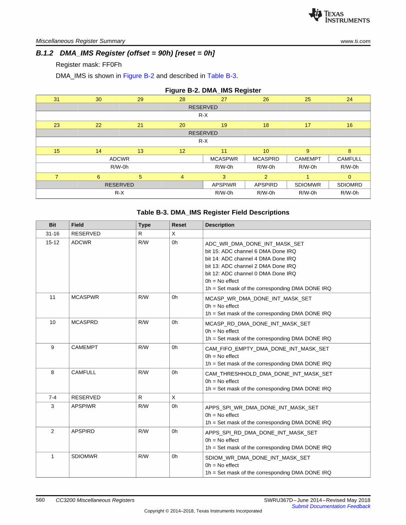
Miscellaneous Register Summary www.ti.com
560 SWRU367D–June 2014–Revised May 2018Submit Documentation Feedback
Copyright © 2014–2018, Texas Instruments Incorporated
CC3200 Miscellaneous Registers
B.1.2 DMA_IMS Register (offset = 90h) [reset = 0h]Register mask: FF0Fh
DMA_IMS is shown in Figure B-2 and described in Table B-3.
Figure B-2. DMA_IMS Register31 30 29 28 27 26 25 24
RESERVEDR-X
23 22 21 20 19 18 17 16RESERVED
R-X
15 14 13 12 11 10 9 8ADCWR MCASPWR MCASPRD CAMEMPT CAMFULLR/W-0h R/W-0h R/W-0h R/W-0h R/W-0h
7 6 5 4 3 2 1 0RESERVED APSPIWR APSPIRD SDIOMWR SDIOMRD
R-X R/W-0h R/W-0h R/W-0h R/W-0h
Table B-3. DMA_IMS Register Field Descriptions
Bit Field Type Reset Description31-16 RESERVED R X15-12 ADCWR R/W 0h ADC_WR_DMA_DONE_INT_MASK_SET
bit 15: ADC channel 6 DMA Done IRQbit 14: ADC channel 4 DMA Done IRQbit 13: ADC channel 2 DMA Done IRQbit 12: ADC channel 0 DMA Done IRQ0h = No effect1h = Set mask of the corresponding DMA DONE IRQ
11 MCASPWR R/W 0h MCASP_WR_DMA_DONE_INT_MASK_SET0h = No effect1h = Set mask of the corresponding DMA DONE IRQ
10 MCASPRD R/W 0h MCASP_RD_DMA_DONE_INT_MASK_SET0h = No effect1h = Set mask of the corresponding DMA DONE IRQ
9 CAMEMPT R/W 0h CAM_FIFO_EMPTY_DMA_DONE_INT_MASK_SET0h = No effect1h = Set mask of the corresponding DMA DONE IRQ
8 CAMFULL R/W 0h CAM_THRESHHOLD_DMA_DONE_INT_MASK_SET0h = No effect1h = Set mask of the corresponding DMA DONE IRQ
7-4 RESERVED R X3 APSPIWR R/W 0h APPS_SPI_WR_DMA_DONE_INT_MASK_SET
0h = No effect1h = Set mask of the corresponding DMA DONE IRQ
2 APSPIRD R/W 0h APPS_SPI_RD_DMA_DONE_INT_MASK_SET0h = No effect1h = Set mask of the corresponding DMA DONE IRQ
1 SDIOMWR R/W 0h SDIOM_WR_DMA_DONE_INT_MASK_SET0h = No effect1h = Set mask of the corresponding DMA DONE IRQ
www.ti.com Miscellaneous Register Summary
561SWRU367D–June 2014–Revised May 2018Submit Documentation Feedback
Copyright © 2014–2018, Texas Instruments Incorporated
CC3200 Miscellaneous Registers
Table B-3. DMA_IMS Register Field Descriptions (continued)Bit Field Type Reset Description0 SDIOMRD R/W 0h SDIOM_RD_DMA_DONE_INT_MASK_SET
0h = No effect1h = Set mask of the corresponding DMA DONE IRQ

Miscellaneous Register Summary www.ti.com
562 SWRU367D–June 2014–Revised May 2018Submit Documentation Feedback
Copyright © 2014–2018, Texas Instruments Incorporated
CC3200 Miscellaneous Registers
B.1.3 DMA_IMC Register (offset = 94h) [reset = 0h]Register mask: FF0Fh
DMA_IMC is shown in Figure B-3 and described in Table B-4.
Figure B-3. DMA_IMC Register31 30 29 28 27 26 25 24
RESERVEDR-X
23 22 21 20 19 18 17 16RESERVED
R-X
15 14 13 12 11 10 9 8ADCWR MCASPWR MCASPRD CAMEMPT CAMFULLR/W-0h R/W-0h R/W-0h R/W-0h R/W-0h
7 6 5 4 3 2 1 0RESERVED APSPIWR APSPIRD SDIOMWR SDIOMRD
R-X R/W-0h R/W-0h R/W-0h R/W-0h
Table B-4. DMA_IMC Register Field Descriptions
Bit Field Type Reset Description31-16 RESERVED R X15-12 ADCWR R/W 0h ADC_WR_DMA_DONE_INT_MASK_CLR
bit 15: ADC channel 6 DMA Done IRQ maskbit 14: ADC channel 4 DMA Done IRQ maskbit 13: ADC channel 2 DMA Done IRQ maskbit 12: ADC channel 0 DMA Done IRQ mask0h = No effect1h = Clear mask of the corresponding DMA DONE IRQ
11 MCASPWR R/W 0h MCASP_WR_DMA_DONE_INT_MASK_CLR0h = No effect1h = Clear mask of the corresponding DMA DONE IRQ
10 MCASPRD R/W 0h MCASP_RD_DMA_DONE_INT_MASK_CLR0h = No effect1h = Clear mask of the corresponding DMA DONE IRQ
9 CAMEMPT R/W 0h CAM_FIFO_EMPTY_DMA_DONE_INT_MASK_CLR0h = No effect1h = Clear mask of the corresponding DMA DONE IRQ
8 CAMFULL R/W 0h CAM_THRESHHOLD_DMA_DONE_INT_MASK_CLR0h = No effect1h = Clear mask of the corresponding DMA DONE IRQ
7-4 RESERVED R X3 APSPIWR R/W 0h APPS_SPI_WR_DMA_DONE_INT_MASK_CLR
0h = No effect1h = Clear mask of the corresponding DMA DONE IRQ
2 APSPIRD R/W 0h APPS_SPI_RD_DMA_DONE_INT_MASK_CLR0h = No effect1h = Clear mask of the corresponding DMA DONE IRQ
1 SDIOMWR R/W 0h SDIOM_WR_DMA_DONE_INT_MASK_CLR0h = No effect1h = Clear mask of the corresponding DMA DONE IRQ

www.ti.com Miscellaneous Register Summary
563SWRU367D–June 2014–Revised May 2018Submit Documentation Feedback
Copyright © 2014–2018, Texas Instruments Incorporated
CC3200 Miscellaneous Registers
Table B-4. DMA_IMC Register Field Descriptions (continued)Bit Field Type Reset Description0 SDIOMRD R/W 0h SDIOM_RD_DMA_DONE_INT_MASK_CLR
0h = No effect1h = Clear mask of the corresponding DMA DONE IRQ

Miscellaneous Register Summary www.ti.com
564 SWRU367D–June 2014–Revised May 2018Submit Documentation Feedback
Copyright © 2014–2018, Texas Instruments Incorporated
CC3200 Miscellaneous Registers
B.1.4 DMA_ICR Register (offset = 9Ch) [reset = 0h]Register mask: FF0Fh
DMA_ICR is shown in Figure B-4 and described in Table B-5.
Figure B-4. DMA_ICR Register31 30 29 28 27 26 25 24
RESERVEDR-X
23 22 21 20 19 18 17 16RESERVED
R-X
15 14 13 12 11 10 9 8ADCWR MCASPWR MCASPRD CAMEMPT CAMFULLR/W-0h R/W-0h R/W-0h R/W-0h R/W-0h
7 6 5 4 3 2 1 0RESERVED APSPIWR APSPIRD SDIOMWR SDIOMRD
R-X R/W-0h R/W-0h R/W-0h R/W-0h
Table B-5. DMA_ICR Register Field Descriptions
Bit Field Type Reset Description31-16 RESERVED R X15-12 ADCWR R/W 0h ADC_WR_DMA_DONE_INT_ACK
bit 15: ADC channel 6 DMA Done IRQbit 14: ADC channel 4 DMA Done IRQbit 13: ADC channel 2 DMA Done IRQbit 12: ADC channel 0 DMA Done IRQ0h = No effect1h = Clear corresponding interrupt
11 MCASPWR R/W 0h MCASP_WR_DMA_DONE_INT_ACK0h = No effect1h = Clear corresponding interrupt
10 MCASPRD R/W 0h MCASP_RD_DMA_DONE_INT_ACK0h = No effect1h = Clear corresponding interrupt
9 CAMEMPT R/W 0h CAM_FIFO_EMPTY_DMA_DONE_INT_ACK0h = No effect1h = Clear corresponding interrupt
8 CAMFULL R/W 0h CAM_THRESHHOLD_DMA_DONE_INT_ACK0h = No effect1h = Clear corresponding interrupt
7-4 RESERVED R X3 APSPIWR R/W 0h APPS_SPI_WR_DMA_DONE_INT_ACK
0h = No effect1h = Clear corresponding interrupt
2 APSPIRD R/W 0h APPS_SPI_RD_DMA_DONE_INT_ACK0h = No effect1h = Clear corresponding interrupt
1 SDIOMWR R/W 0h SDIOM_WR_DMA_DONE_INT_ACK0h = No effect1h = Clear corresponding interrupt
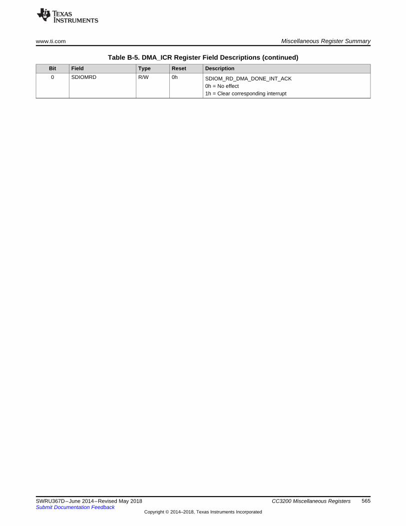
www.ti.com Miscellaneous Register Summary
565SWRU367D–June 2014–Revised May 2018Submit Documentation Feedback
Copyright © 2014–2018, Texas Instruments Incorporated
CC3200 Miscellaneous Registers
Table B-5. DMA_ICR Register Field Descriptions (continued)Bit Field Type Reset Description0 SDIOMRD R/W 0h SDIOM_RD_DMA_DONE_INT_ACK
0h = No effect1h = Clear corresponding interrupt
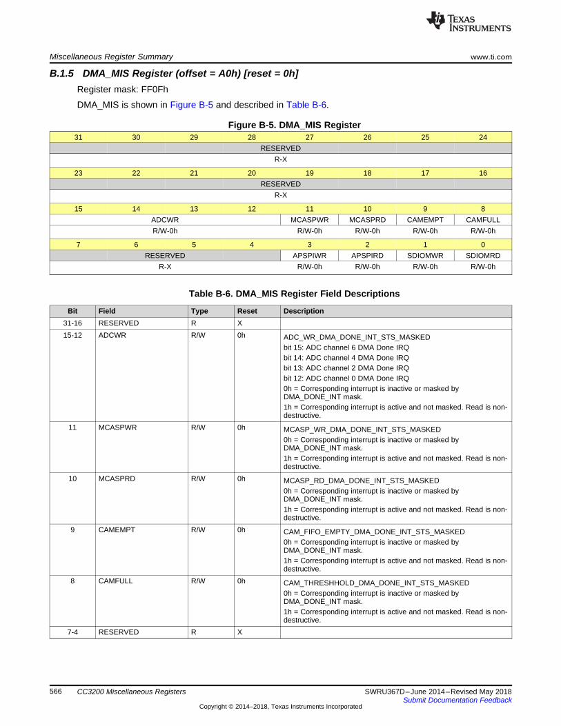
Miscellaneous Register Summary www.ti.com
566 SWRU367D–June 2014–Revised May 2018Submit Documentation Feedback
Copyright © 2014–2018, Texas Instruments Incorporated
CC3200 Miscellaneous Registers
B.1.5 DMA_MIS Register (offset = A0h) [reset = 0h]Register mask: FF0Fh
DMA_MIS is shown in Figure B-5 and described in Table B-6.
Figure B-5. DMA_MIS Register31 30 29 28 27 26 25 24
RESERVEDR-X
23 22 21 20 19 18 17 16RESERVED
R-X
15 14 13 12 11 10 9 8ADCWR MCASPWR MCASPRD CAMEMPT CAMFULLR/W-0h R/W-0h R/W-0h R/W-0h R/W-0h
7 6 5 4 3 2 1 0RESERVED APSPIWR APSPIRD SDIOMWR SDIOMRD
R-X R/W-0h R/W-0h R/W-0h R/W-0h
Table B-6. DMA_MIS Register Field Descriptions
Bit Field Type Reset Description31-16 RESERVED R X15-12 ADCWR R/W 0h ADC_WR_DMA_DONE_INT_STS_MASKED
bit 15: ADC channel 6 DMA Done IRQbit 14: ADC channel 4 DMA Done IRQbit 13: ADC channel 2 DMA Done IRQbit 12: ADC channel 0 DMA Done IRQ0h = Corresponding interrupt is inactive or masked byDMA_DONE_INT mask.1h = Corresponding interrupt is active and not masked. Read is non-destructive.
11 MCASPWR R/W 0h MCASP_WR_DMA_DONE_INT_STS_MASKED0h = Corresponding interrupt is inactive or masked byDMA_DONE_INT mask.1h = Corresponding interrupt is active and not masked. Read is non-destructive.
10 MCASPRD R/W 0h MCASP_RD_DMA_DONE_INT_STS_MASKED0h = Corresponding interrupt is inactive or masked byDMA_DONE_INT mask.1h = Corresponding interrupt is active and not masked. Read is non-destructive.
9 CAMEMPT R/W 0h CAM_FIFO_EMPTY_DMA_DONE_INT_STS_MASKED0h = Corresponding interrupt is inactive or masked byDMA_DONE_INT mask.1h = Corresponding interrupt is active and not masked. Read is non-destructive.
8 CAMFULL R/W 0h CAM_THRESHHOLD_DMA_DONE_INT_STS_MASKED0h = Corresponding interrupt is inactive or masked byDMA_DONE_INT mask.1h = Corresponding interrupt is active and not masked. Read is non-destructive.
7-4 RESERVED R X

www.ti.com Miscellaneous Register Summary
567SWRU367D–June 2014–Revised May 2018Submit Documentation Feedback
Copyright © 2014–2018, Texas Instruments Incorporated
CC3200 Miscellaneous Registers
Table B-6. DMA_MIS Register Field Descriptions (continued)Bit Field Type Reset Description3 APSPIWR R/W 0h APPS_SPI_WR_DMA_DONE_INT_STS_MASKED
0h = Corresponding interrupt is inactive or masked byDMA_DONE_INT mask.1h = Corresponding interrupt is active and not masked. Read is non-destructive.
2 APSPIRD R/W 0h APPS_SPI_RD_DMA_DONE_INT_STS_MASKED0h = Corresponding interrupt is inactive or masked byDMA_DONE_INT mask.1h = Corresponding interrupt is active and not masked. Read is non-destructive.
1 SDIOMWR R/W 0h SDIOM_WR_DMA_DONE_INT_STS_MASKED0h = Corresponding interrupt is inactive or masked byDMA_DONE_INT mask.1h = Corresponding interrupt is active and not masked. Read is non-destructive.
0 SDIOMRD R/W 0h SDIOM_RD_DMA_DONE_INT_STS_MASKED0h = Corresponding interrupt is inactive or masked byDMA_DONE_INT mask.1h = Corresponding interrupt is active and not masked. Read is non-destructive.

Miscellaneous Register Summary www.ti.com
568 SWRU367D–June 2014–Revised May 2018Submit Documentation Feedback
Copyright © 2014–2018, Texas Instruments Incorporated
CC3200 Miscellaneous Registers
B.1.6 DMA_RIS Register (offset = A4h) [reset = 0h]Register mask: FF0Fh
DMA_RIS is shown in Figure B-6 and described in Table B-7.
Figure B-6. DMA_RIS Register31 30 29 28 27 26 25 24
RESERVEDR-X
23 22 21 20 19 18 17 16RESERVED
R-X
15 14 13 12 11 10 9 8ADCWR MCASPWR MCASPRD CAMEMPT CAMFULLR/W-0h R/W-0h R/W-0h R/W-0h R/W-0h
7 6 5 4 3 2 1 0RESERVED APSPIWR APSPIRD SDIOMWR SDIOMRD
R-X R/W-0h R/W-0h R/W-0h R/W-0h
Table B-7. DMA_RIS Register Field Descriptions
Bit Field Type Reset Description31-16 RESERVED R X15-12 ADCWR R/W 0h ADC_WR_DMA_DONE_INT_STS_RAW
bit 15: ADC channel 6 DMA Done IRQbit 14: ADC channel 4 DMA Done IRQbit 13: ADC channel 2 DMA Done IRQbit 12: ADC channel 0 DMA Done IRQ0h = Corresponding interrupt is inactive.1h = Corresponding interrupt is active. Read is non-destructive.
11 MCASPWR R/W 0h MCASP_WR_DMA_DONE_INT_STS_RAW0h = Corresponding interrupt is inactive.1h = Corresponding interrupt is active. Read is non-destructive.
10 MCASPRD R/W 0h MCASP_RD_DMA_DONE_INT_STS_RAW0h = Corresponding interrupt is inactive.1h = Corresponding interrupt is active. Read is non-destructive.
9 CAMEMPT R/W 0h CAM_FIFO_EMPTY_DMA_DONE_INT_STS_RAW0h = Corresponding interrupt is inactive.1h = Corresponding interrupt is active. Read is non-destructive.
8 CAMFULL R/W 0h CAM_THRESHHOLD_DMA_DONE_INT_STS_RAW0h = Corresponding interrupt is inactive.1h = Corresponding interrupt is active. Read is non-destructive.
7-4 RESERVED R X3 APSPIWR R/W 0h APPS_SPI_WR_DMA_DONE_INT_STS_RAW
0h = Corresponding interrupt is inactive.1h = Corresponding interrupt is active. Read is non-destructive.
2 APSPIRD R/W 0h APPS_SPI_RD_DMA_DONE_INT_STS_RAW0h = Corresponding interrupt is inactive.1h = Corresponding interrupt is active. Read is non-destructive.
1 SDIOMWR R/W 0h SDIOM_WR_DMA_DONE_INT_STS_RAW0h = Corresponding interrupt is inactive.1h = Corresponding interrupt is active. Read is non-destructive.

www.ti.com Miscellaneous Register Summary
569SWRU367D–June 2014–Revised May 2018Submit Documentation Feedback
Copyright © 2014–2018, Texas Instruments Incorporated
CC3200 Miscellaneous Registers
Table B-7. DMA_RIS Register Field Descriptions (continued)Bit Field Type Reset Description0 SDIOMRD R/W 0h SDIOM_RD_DMA_DONE_INT_STS_RAW
0h = Corresponding interrupt is inactive.1h = Corresponding interrupt is active. Read is non-destructive.
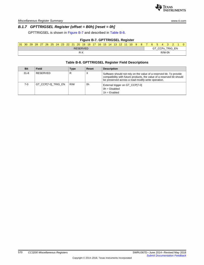
Miscellaneous Register Summary www.ti.com
570 SWRU367D–June 2014–Revised May 2018Submit Documentation Feedback
Copyright © 2014–2018, Texas Instruments Incorporated
CC3200 Miscellaneous Registers
B.1.7 GPTTRIGSEL Register (offset = B0h) [reset = 0h]GPTTRIGSEL is shown in Figure B-7 and described in Table B-8.
Figure B-7. GPTTRIGSEL Register31 30 29 28 27 26 25 24 23 22 21 20 19 18 17 16 15 14 13 12 11 10 9 8 7 6 5 4 3 2 1 0
RESERVED GT_CCPx_TRIG_ENR-X R/W-0h
Table B-8. GPTTRIGSEL Register Field Descriptions
Bit Field Type Reset Description31-8 RESERVED R X Software should not rely on the value of a reserved bit. To provide
compatibility with future products, the value of a reserved bit shouldbe preserved across a read-modify-write operation.
7-0 GT_CCP[7-0]_TRIG_EN R/W 0h External trigger on GT_CCP[7-0]0h = Disabled1h = Enabled
www.ti.com Revision History
571SWRU367D–June 2014–Revised May 2018Submit Documentation Feedback
Copyright © 2014–2018, Texas Instruments Incorporated
Revision History
Revision HistoryNOTE: Page numbers for previous revisions may differ from page numbers in the current version.
Changes from March 31, 2016 to May 30, 2018 (from C Revision (March 2016) to D Revision) ................................. Page
• Updated Debug Interface section. ..................................................................................................... 30• Updated CC3200 Application Processor Interrupts table........................................................................... 46• Updated CPUID Register Field Descriptions table. ................................................................................ 77• Added DMA_(OFFSET_FROM_DMA_BASE_ADDRESS) Registers section. ................................................ 115• Updated BRK bit of UARTLCRH Register Field Description. .................................................................... 173• Updated GPTMTBMR Register....................................................................................................... 301• Updated GPTTRIGSEL Register. .................................................................................................... 570

IMPORTANT NOTICE FOR TI DESIGN INFORMATION AND RESOURCES
Texas Instruments Incorporated (‘TI”) technical, application or other design advice, services or information, including, but not limited to,reference designs and materials relating to evaluation modules, (collectively, “TI Resources”) are intended to assist designers who aredeveloping applications that incorporate TI products; by downloading, accessing or using any particular TI Resource in any way, you(individually or, if you are acting on behalf of a company, your company) agree to use it solely for this purpose and subject to the terms ofthis Notice.TI’s provision of TI Resources does not expand or otherwise alter TI’s applicable published warranties or warranty disclaimers for TIproducts, and no additional obligations or liabilities arise from TI providing such TI Resources. TI reserves the right to make corrections,enhancements, improvements and other changes to its TI Resources.You understand and agree that you remain responsible for using your independent analysis, evaluation and judgment in designing yourapplications and that you have full and exclusive responsibility to assure the safety of your applications and compliance of your applications(and of all TI products used in or for your applications) with all applicable regulations, laws and other applicable requirements. Yourepresent that, with respect to your applications, you have all the necessary expertise to create and implement safeguards that (1)anticipate dangerous consequences of failures, (2) monitor failures and their consequences, and (3) lessen the likelihood of failures thatmight cause harm and take appropriate actions. You agree that prior to using or distributing any applications that include TI products, youwill thoroughly test such applications and the functionality of such TI products as used in such applications. TI has not conducted anytesting other than that specifically described in the published documentation for a particular TI Resource.You are authorized to use, copy and modify any individual TI Resource only in connection with the development of applications that includethe TI product(s) identified in such TI Resource. NO OTHER LICENSE, EXPRESS OR IMPLIED, BY ESTOPPEL OR OTHERWISE TOANY OTHER TI INTELLECTUAL PROPERTY RIGHT, AND NO LICENSE TO ANY TECHNOLOGY OR INTELLECTUAL PROPERTYRIGHT OF TI OR ANY THIRD PARTY IS GRANTED HEREIN, including but not limited to any patent right, copyright, mask work right, orother intellectual property right relating to any combination, machine, or process in which TI products or services are used. Informationregarding or referencing third-party products or services does not constitute a license to use such products or services, or a warranty orendorsement thereof. Use of TI Resources may require a license from a third party under the patents or other intellectual property of thethird party, or a license from TI under the patents or other intellectual property of TI.TI RESOURCES ARE PROVIDED “AS IS” AND WITH ALL FAULTS. TI DISCLAIMS ALL OTHER WARRANTIES ORREPRESENTATIONS, EXPRESS OR IMPLIED, REGARDING TI RESOURCES OR USE THEREOF, INCLUDING BUT NOT LIMITED TOACCURACY OR COMPLETENESS, TITLE, ANY EPIDEMIC FAILURE WARRANTY AND ANY IMPLIED WARRANTIES OFMERCHANTABILITY, FITNESS FOR A PARTICULAR PURPOSE, AND NON-INFRINGEMENT OF ANY THIRD PARTY INTELLECTUALPROPERTY RIGHTS.TI SHALL NOT BE LIABLE FOR AND SHALL NOT DEFEND OR INDEMNIFY YOU AGAINST ANY CLAIM, INCLUDING BUT NOTLIMITED TO ANY INFRINGEMENT CLAIM THAT RELATES TO OR IS BASED ON ANY COMBINATION OF PRODUCTS EVEN IFDESCRIBED IN TI RESOURCES OR OTHERWISE. IN NO EVENT SHALL TI BE LIABLE FOR ANY ACTUAL, DIRECT, SPECIAL,COLLATERAL, INDIRECT, PUNITIVE, INCIDENTAL, CONSEQUENTIAL OR EXEMPLARY DAMAGES IN CONNECTION WITH ORARISING OUT OF TI RESOURCES OR USE THEREOF, AND REGARDLESS OF WHETHER TI HAS BEEN ADVISED OF THEPOSSIBILITY OF SUCH DAMAGES.You agree to fully indemnify TI and its representatives against any damages, costs, losses, and/or liabilities arising out of your non-compliance with the terms and provisions of this Notice.This Notice applies to TI Resources. Additional terms apply to the use and purchase of certain types of materials, TI products and services.These include; without limitation, TI’s standard terms for semiconductor products http://www.ti.com/sc/docs/stdterms.htm), evaluationmodules, and samples (http://www.ti.com/sc/docs/sampterms.htm).
Mailing Address: Texas Instruments, Post Office Box 655303, Dallas, Texas 75265Copyright © 2018, Texas Instruments Incorporated