Ian Bird Trigger, Online, Offline Computing Workshop CERN, 5 th September 2014.
date post
19-Dec-2015Category
view
216download
0
CA
RE s
teeri
ng
Sep
tem
ber
17th
20
08
1
NED Status Report
Thierry Boutboul(CERN)
CERN17 September 2008

CA
RE s
teeri
ng
Sep
tem
ber
17th
20
08
2
CARE/NED JRA
•Following the 2003 EU peer review, the scope of the NED
program was revised to focus on Nb3Sn conductor and
insulation development. •The NED JRA has been articulated around four Work Packages
and one Working Group
1 Management & Communication (M&C),
2 Thermal Studies and Quench Protection (TSQP),
3 Conductor Development (CD),
4 Insulation Development and Implementation (IDI),
5 Magnet Design and Optimization (MDO) Working
Group. • It involves 7 institutes (8 laboratories)
• Total budget: ~2 M€; EU grant: 979 k€ (over ~3 years).

CA
RE s
teeri
ng
Sep
tem
ber
17th
20
08
3
NED/TSQP Work Package
• The Thermal Studies part of the TSQP Work Package was completed with the publication of the final report in December 2007 (CARE-Report-2007-033-NED)(CEA and WUT; Task Leader: B. Baudouy, CEA)
• The quench computation task was already completed before
(INFN-Mi; Task Leader: G. Volpini).

CA
RE s
teeri
ng
Sep
tem
ber
17th
20
08
4
NED-CD Work Package
• The CD Work Package includes two main Tasks – conductor development
two industrial contracts under CERN supervision: Alstom/MSA (F) and EAS/SMI (NL/D); Task Leader: L. Oberli
– conductor characterization (CEA, INFN-Ge, INFN-Mi, and TEU; Task Leader: A. den Ouden, TEU)
• It is the core of the Program and absorbs ~70% of the EU funding.
• It is complemented by two extensions of scope – FE wire model development to simulate cabling effects
(INFN-Ge & CERN; Task Leader: S. Farinon, INFN-Ge), – heat treatment study
(CERN; Task Leader: C. Scheuerlein).

CA
RE s
teeri
ng
Sep
tem
ber
17th
20
08
5
NED-CD: Status of the SMI contract (1)
• Following successful R&D step 2 including the cabling trial of a 40-strand Rutherford cable (LBNL), EAS/SMI was awarded the green light to launch the final strand production in fall 2007.
• Final strand manufacturing (12.7 km of strand overall) is currently underway and the full strand delivery to CERN has taken a few months delay (was expected by summer 2008).
• A first 1000 m long strand, B228, produced partly at Hanau (EAS) and partly at Enschede (SMI) delivered to CERN in April 2008 into 2 strand lengths (400 m + 600 m).
• A second strand, B230 (1650 m), was completely produced at Hanau, except final strand drawing to nominal diameter. This strand was delivered to CERN in July 2008 into 4 strand lengths (705 + 314 + 305 + 323 m). Since July 2008, equipment transfer from SMI to EAS was completed.

CA
RE s
teeri
ng
Sep
tem
ber
17th
20
08
6
NED-CD: Status of the SMI contract (2)
• An additional strand of 3.5 km is currently under fabrication at Hanau (final steps). It is expected to be delivered at the beginning of October 2008.
• The remaining 6.6 km of PIT strand are currently in early steps of production. They are expected to be delivered to CERN into two strand batches by the end of 2008.
• The strands B228 and B230 (partly) were used to produce at CERN a 14-strand cable (9.7 mm width and 2.2 mm thickness) for Short Model Coil (SMC) program. A 138 m long SMC cable was successfully produced in early September 2008.

CA
RE s
teeri
ng
Sep
tem
ber
17th
20
08
7
NED-CD: Status of the Alstom contract (1)
• During Step 2, Alstom considered two fabrication processes: one with cold work only (Way 1) and the second based on hot extrusion.
• With cold work method, Alstom produced a strand which included 78 sub-elements (~ 85 µm in diameter). This fabrication was characterized by workability problems (numerous breakages). This strand (binary Nb3Sn) showed a non-copper Jc ~ 2000 A/mm2 at 12 T and 4.2 K.
• The second way (extrusion) used to guarantee fair cohesion between Nb barrier and Cu can, especially important when increasing the number of sub-elements (to decrease filament size down to 50 µm, as requested by specification).
• Then, B1/63468 strand was produced into a single length of 1300 m, showing a very fair workability. This strand includes 246 sub-elements (~ 54 µm in diameter). In order to further check the strand workability, the B1/63468 was successfully drawn down to 0.8 mm diameter, corresponding to 35 µm in diameter sub-elements!!

CA
RE s
teeri
ng
Sep
tem
ber
17th
20
08
8
NED-CD: Status of the Alstom contract (2)
• However, disappointing critical current density for B1/63468: Jc~1500 A/mm2 at 12 T and 4.2 K.
• Many efforts done at CERN to try to optimize heat treatment but without significant success (1600 A/mm2 maximal value reached).
• The main reason for this low Jc seems to be the big Nb3Sn grains observed by means of SEM (poor pinning). Therefore using Ta additions, leading to ternary Nb3Sn, should limit grain growth and then enhance Jc (up to 40-50 %).
• Therefore, two billets currently fabricated by Alstom by cold drawing process with Nb-Ta filaments to get ternary Nb3Sn phase. Around 1.5 km long and 6 km long strands respectively expected by November and December 2008.
• Extrusion process continued in parallel (Ta-alloyed Nb3Sn). Raw material (especially Nb tubes) already ordered from supplier. 15-20 km of strand expected by March 2009.

CA
RE s
teeri
ng
Sep
tem
ber
17th
20
08
9
NED-CD: Planning of final strand delivery
Firm
Total [km]
Delivered [km]
10/08
11/08
12/08
03/09
EAS/SMI 12.7 2.6 3.5 - 6.6 -
Alstom 24 - - 1.5 6 15-20

CA
RE s
teeri
ng
Sep
tem
ber
17th
20
08
10
NED-CD: Conductor characterization (1)
EAS/SMI B215 wire
• B215 is the successful prototype wire developed by SMI during Step 2. According to its design, the final strand is currently produced. This strand has 288 filaments (~ 50 µm), 84 h @ 675 oC: Jc ~ 2500 A/mm2.
• Heat treatment optimization studies at CERN: general trend was to decrease reaction temperature but increase duration to try to decrease Nb3Sn grain size.
• 320 h @ 625 oC: - 12 T and 4.2 K: Ic > 1500 A, Jc > 2700 A/mm2, + 10 %!!
- 15 T and 4.2 K: Ic > 818 A (NED spec.), Jc ~ 1500 A/mm2
- RRR ~ 220 (vs 80 for 84 h @ 675 oC): much better for stability
• Reasonable cabling degradation of 5-6 % (as compared to 10-13 % for 84 h @ 675 oC).

CA
RE s
teeri
ng
Sep
tem
ber
17th
20
08
11
NED-CD: Conductor characterization (2)
EAS/SMI B215 wire (continuation)
0
200
400
600
800
1000
1200
1400
1600
1800
10 12 14 16 18 20 22 24
Applied field [T]
Cri
tica
l cu
rren
t [A
]
Nijmegen, 320 h @ 625 C
Specification
Geneva, 84 h @ 675 C
> 120> 200> 8181.25± 0.10< 501.250 ±0.004
Specification
~ 130~ 220823-8591.2249.81.258625 oC/320 h
30-6070-807561.2249.81.258675 oC/84 h
RRR, extr.RRR, virgin
Ic, 15 T [A]
Cu/non-CuDeff [µm]D [mm]HT
> 120> 200> 8181.25± 0.10< 501.250 ±0.004
Specification
~ 130~ 220823-8591.2249.81.258625 oC/320 h
30-6070-807561.2249.81.258675 oC/84 h
RRR, extr.RRR, virgin
Ic, 15 T [A]
Cu/non-CuDeff [µm]D [mm]HT
Stringent NED specification fulfilled!!
Bc2K = 26.3 T
Courtesy of C. Senatore and R. Flukiger (Geneva Univ.)

CA
RE s
teeri
ng
Sep
tem
ber
17th
20
08
12
NED-CD: Conductor characterization (3)
EAS/SMI B215 wire (end)SEM: Polished and fractured samples examined for standard and
modified HT.
675 oC/84 h 625 oC/320 h
Un-reacted barrier ratio 23 % of total filament 25 % of total filament
Sn content 24.2 at. % Sn 24.7 at. % Sn
Coarse grain ratio ~ 30 % of A15 phase ~ 30 % of A15 phase
Mean fine grain size ~ 180 nm ~ 160 nm
Sample with optimized HT: less reacted Nb3Sn but with higher quality: higher Sn content, Bc2
K, Tc and smaller grain size (160 nm vs 180 nm)
coarse grain (~ 1-2 µm) fine grain (~ 200 nm)
CA
RE s
teeri
ng
Sep
tem
ber
17th
20
08
13
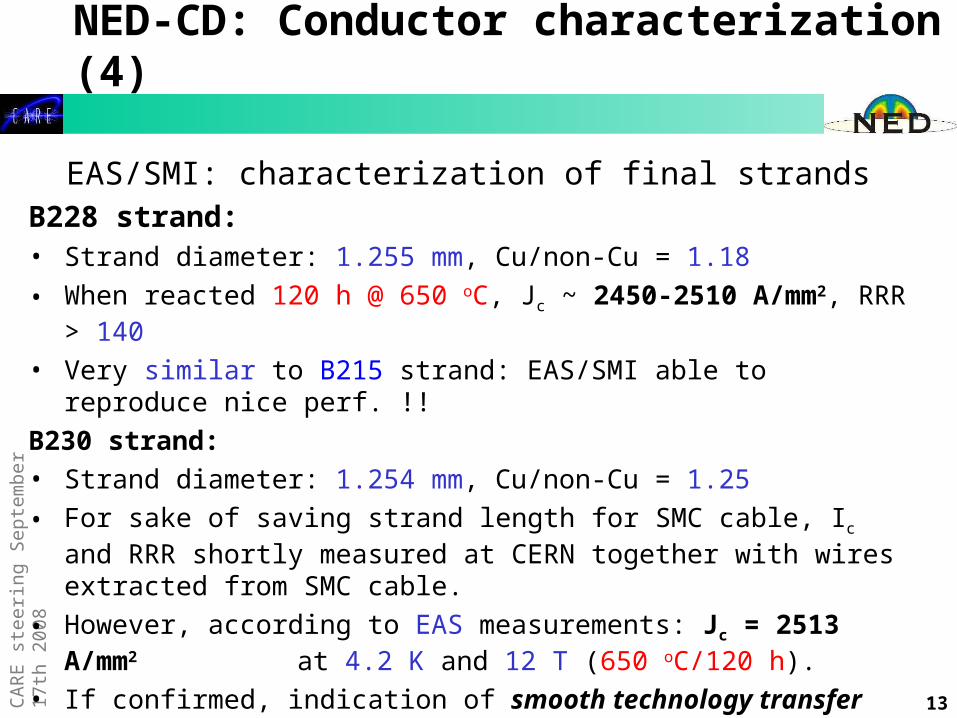
NED-CD: Conductor characterization (4)
EAS/SMI: characterization of final strandsB228 strand: • Strand diameter: 1.255 mm, Cu/non-Cu = 1.18
• When reacted 120 h @ 650 oC, Jc ~ 2450-2510 A/mm2, RRR > 140
• Very similar to B215 strand: EAS/SMI able to reproduce nice perf. !!
B230 strand:• Strand diameter: 1.254 mm, Cu/non-Cu = 1.25
• For sake of saving strand length for SMC cable, Ic and RRR shortly measured at CERN together with wires extracted from SMC cable.
• However, according to EAS measurements: Jc = 2513 A/mm2 at 4.2 K and 12 T (650 oC/120 h).
• If confirmed, indication of smooth technology transfer from SMI to EAS.

CA
RE s
teeri
ng
Sep
tem
ber
17th
20
08
14
NED-IDI Work Package (1)
• The Insulation Development and Implementation Work Package includes two main Tasks
– studies on “conventional” insulation systems relying on ceramic or glass fiber tape and vacuum-impregnation by epoxy resin (CCLRC/RAL; Task Leader: S. Canfer)
Completed with a final report in March 2007
– studies on “innovative” insulation systems relying on pre- impregnated fiber tapes and eliminating the need for a vacuum impregnation (CEA; Task Leader: F. Rondeaux).
Completed with a final report in December 2007(CARE-Report-2007-037-NED)

CA
RE s
teeri
ng
Sep
tem
ber
17th
20
08
NED conductor review 4 Nov 2008
The aim of the review is twofold
• Firstly, the NED Nb3Sn conductor development program should be reviewed such that the achievements, the main difficulties and the limitations are brought out.
• Secondly, using the experience of this conductor program, the requirements for new dipoles and quadrupoles and the existing open issues ( eg. stability and stress sensitivity), recommendations for the next steps in Nb3Sn conductor development for accelerator magnets at CERN should be formulated.
15

CA
RE s
teeri
ng
Sep
tem
ber
17th
20
08
NED conductor review: program 4 Nov 2008
1. History of the NED conductor program Luc Oberli
2. Results of the PIT conductor development Thierry Boutboul
3. Results of the IT conductor developmentLuc Oberli
4. Results of the cable development Thierry Boutboul
5. Guidelines on stability Bernardo Bordini
6. Review on stress sensitivity Rene Flukiger
7. Dipole conductor needs: examples for Fresca2 Glyn Kirby
8. Quadrupole conductor needs: examples for HQ Helene Felice
16

CA
RE s
teeri
ng
Sep
tem
ber
17th
20
08
17
Next Step: Short Model Coil SMC
• Participant funding only (formally outside FP6-CARE-NED )
• CCLRC/RAL, CEA and CERN have agreed to manufacture and test a series of LBNL-type Short Model Coils wound from NED-sub-cables so as to investigate – cable and insulation performances in real coil environment, – design limits for transverse and longitudinal loads.
• Coil and cold mass design finished, winding tests with dummy Cu+Nb3Snin progress by RAL-CERN team (with LBNL)Nb3Sn cable done (120 m ready: 3 poles).
Tender for structure components called.First magnet foreseen to be tested in February 2009 at CERN
(Courtesy P. Ferracin, LBNL)
CA
RE s
teeri
ng
Sep
tem
ber
17th
20
08
18
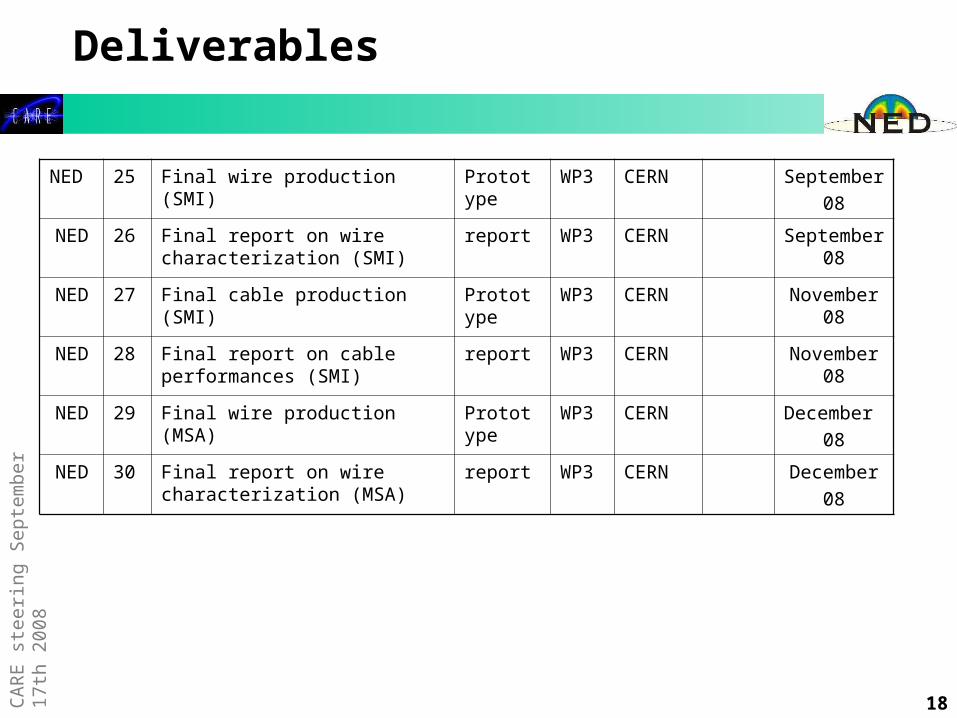
Deliverables
NED 25 Final wire production (SMI) Prototype WP3 CERN September
08
NED 26 Final report on wire characterization (SMI)
report WP3 CERN September 08
NED 27 Final cable production (SMI) Prototype WP3 CERN November 08
NED 28 Final report on cable performances (SMI)
report WP3 CERN November 08
NED 29 Final wire production (MSA) Prototype WP3 CERN December
08
NED 30 Final report on wire characterization (MSA)
report WP3 CERN December
08