CARBON NANOTUBE BASED THIN FILM TRANSISTORS FOR GAS ...
154
I CARBON NANOTUBE BASED THIN FILM TRANSISTORS FOR GAS- SENSING AND ELECTRONIC APPLICATIONS A Dissertation Presented to The Academic Faculty by Jialuo Chen In Partial Fulfillment of the Requirements for the Degree Doctor of Philosophy in the School of Electrical and Computer Engineering Georgia Institute of Technology May 2019 COPYRIGHT © 2019 BY JIALUO CHEN
Transcript of CARBON NANOTUBE BASED THIN FILM TRANSISTORS FOR GAS ...

I
CARBON NANOTUBE BASED THIN FILM TRANSISTORS FOR GAS-
SENSING AND ELECTRONIC APPLICATIONS
A Dissertation
Presented to
The Academic Faculty
by
Jialuo Chen
In Partial Fulfillment
of the Requirements for the Degree
Doctor of Philosophy in the
School of Electrical and Computer Engineering
Georgia Institute of Technology
May 2019
COPYRIGHT © 2019 BY JIALUO CHEN

II
CARBON NANOTUBE BASED THIN FILM TRANSISTORS FOR GAS-
SENSING AND ELECTRONIC APPLICATIONS
Approved by:
Dr. Satish Kumar, Advisor
School of Mechanical Engineering
Georgia Institute of Technology
Dr. Abhijit Chatterjee, Co-advisor
School of Electrical and Computer
Engineering
Georgia Institute of Technology
Dr. Peter J. Hesketh
School of Mechanical Engineering
Georgia Institute of Technology
Dr. Saibal Mukhopadhyay
School of Electrical and Computer
Engineering
Georgia Institute of Technology
Dr. Woon-Hong Yeo
School of Mechanical Engineering
Georgia Institute of Technology
Dr. Asif Islam Khan
School of Electrical and Computer
Engineering
Georgia Institute of Technology
Date Approved: 01/02/2019

III
ACKNOWLEDGEMENTS
I have the most memorable time during last 5 years at Georgia Tech. I would like to take
this opportunity to extend my sincere thanks to those who generously contributed to the work
presented here and gave me endless supports. First, I would like to thank my advisor, Dr. Satish
Kumar, whose enthusiasm and patience in academic researches affects me in so many ways. I feel
deeply attached every time discussing with him, which helps grow maturity in my thoughts. His
incredible guidance and discipline will inspire me in the days to come. Similar gratitude goes to
my co-advisor, Dr. Abhijit Chatterjee, who also gave me the most helps in my hour of need.
I am hugely appreciative to Dr. Peter J Hesketh, Dr. Saibal Mukhopadhyay, Dr Asif Islam
Khan, Dr. Woon-Hong Yeo, and Dr. Seung Woo Lee for allowing me to work in their labs. The
collaborating work with them largely broadens my vision. Profound gratitude goes to Dr. Hang
Chen, Dr. David Gottfried, Chris Yang, Eric Woods, whose patient guidance in cleanroom pave
the way for this work. Sincere thanks go to my fellow labmates Songkil Kim, Tianyuan Liu, Saswat
Mishra for their generous supports in my research. I’m also very thankful to my colleagues Man,
Liang, Zhequan, David, Wenqing, Nitish, and Haoxiang, for creating comfortable office
environment. Special mention goes to Timothy and Eli, who gave me lots of assistances when I
first came to United States.
At last, I am profoundly grateful to my parents for their unconditional love and
understanding all these years. Their truly faith helps me grow whenever success comes or
frustration disturbs.

IV
TABLE OF CONTENTS
ACKNOWLEDGEMENTS III
LIST OF TABLES VIII
LIST OF FIGURES IX
LIST OF SYMBOLS AND ABBREVIATIONS XVIII
SUMMARY XXIV
CHAPTER 1. Introduction 1
1.1 Progress in CNT based Devices 2
1.2 Motivation and Challenges 6
1.2.1 Fabrication 6
1.2.2 Performance Variability 8
1.2.3 Chemical Sensors 9
1.2.4 Flexible Electronics and Sensors 10
1.3 Scope of Current Work 11
CHAPTER 2. BACKGROUND 13
2.1 CNTs and CNT Based Devices 13
2.1.1 Properties of CNTs 13
2.1.2 CNT Network 15
2.1.3 CNT Based Thin Film Transistors 15
2.1.4 Hysteresis of CNT-TFTs 18

V
2.1.5 Variability Analysis of CNT-TFTs 19
2.1.6 Contact Analysis of CNT-TFTs 20
2.1.7 Performance Analysis of CNT-TFTs 22
2.2 Fabrication of CNT-TFTs 24
2.2.1 Photolithography 24
2.2.2 Inkjet Printing 24
2.2.3 Aerosol Jet Printing 26
2.2.4 Screen Printing 27
2.2.5 Roll-to-roll Gravure Printing 28
2.3 Applications 29
2.3.1 Flexible Electronics 29
2.3.2 Sensors and Actuators 31
2.3.3 Radio Frequency Applications 34
2.3.4 Batteries and Energy Devices 34
2.3.5 Other Applications 35
2.4 Contributions of Current Work 36
CHAPTER 3. Performance Variability of CNT-TFTs 39
3.1 Fabrication of CNT-TFTs 39
3.2 I-V Characteristics of CNT-TFTs 41
3.3 CNT Statistics 42
3.3.1 Statistics of CNT Length Distribution 43
3.3.2 Estimation of CNT Network Density 45
3.4 Source of Variation and Variability Analysis 46

VI
3.4.1 M-CNT and S-CNT 50
3.4.2 Threshold Voltage 53
3.4.3 CNT Network Density 56
3.4.4 CNT Mean Length 58
3.4.5 Comprehensive Effects 60
3.5 Closure 61
CHAPTER 4. CNT-TFTs as Gas Sensors 62
4.1 Experiment Setup and Sensing Characteristics 62
4.2 Sample Characteristics and the Sensing Mechanism 64
4.3 Sensor Response Fitting 66
4.4 Consistency of Time Constants for Different Concentration 70
4.5 Gas Identification 72
4.6 Closure 76
CHAPTER 5. FULLY PRINTED CNT-TFTS 77
5.1 Fabrication 77
5.1.1 Fabrication Process 78
5.1.2 Fabrication Details 79
5.2 Morphologies and Performance 83
5.3 Optimization of Printed xdi-dcs Thin Film 85
5.4 Closure 91
CHAPTER 6. FULLY PRINTED GAS SENSORS 93
6.1 Fabrication 93

VII
6.2 Experimental Setup 97
6.3 Sensor Responses 100
6.4 Variability of Sensor Responses 101
6.5 Closure 105
CHAPTER 7. SUMMARY AND FUTURE WORK 107
7.1 Summary of Current Work 107
7.2 Future Work 110
7.2.1 Optimization and Improvement of Fully Printed CNT-TFTs 110
7.2.2 Mechanical Test of Flexible CNT-TFTs 111
7.2.3 Gas Sensing of Flexible CNT Sensors under Stress 111
7.2.4 Mixed Gas Sensing 113
REFERENCES 114

VIII
LIST OF TABLES
Table 2.1 Summary of selected sensing performance (N/S = Not-stated) [25] ............................ 31
Table 4.1 Common time constants at different gas concentration in each state and the
corresponding fitting errors........................................................................................................... 69
Table 6.1 Fabrication comparison among PL, AJP, and IJP ........................................................ 97

IX
LIST OF FIGURES
Figure 1.1 Schematic of a CNT-TFT with randomly distributed CNT network. W is channel width,
L is channel length, Vds is drain voltage, Vgs is gate voltage, and GND is grounded. ................... 1
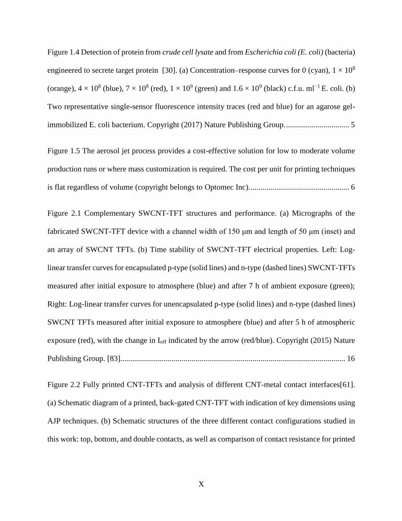
Figure 1.2 Structure and performance of 10-nm CNT based complementary metal-oxide
semiconductor (CMOS) FETs [9]. (a) The cross sections of a p-type FET, n-type FET, and gate
stack; gate length 10 nm, channel length 20 nm. (b) Transfer characteristics of typical CMOS FETs
fabricated on a s-SWCNT with a diameter of 1.3 nm at a drain bias Vds = ±0.4 V. The solid blue
and green curves represent CNT p-type and n-type FETs, respectively. (c and d) Comparison of
10-nm CNT CMOS FETs and commercial Si CMOS transistors of Intel’s 14-nm (22) (solid black
curve) and 22-nm nodes (23) (solid maroon curve). The on currents of n-FETs for CNT, Si 14-nm
node, and Si 22-nm node are 1.16 mA/mm (supply voltage Vdd = 0.4 V, 125 CNTs/mm), 1.1
mA/mm (Vdd = 0.7 V), and 1.03mA/mm (Vdd = 0.8 V), respectively. The on-currents of p-FETs
for CNT, Si 14-nm node, and Si 22-nm node are 0.76 mA/mm (Vdd = 0.4 V, 125 CNTs/mm), 0.96
mA/mm (Vdd = 0.7 V), and 0.83mA/mm (Vdd = 0.8 V), respectively. CNT CMOS FETs and 14-
and 22-nm Si CMOS FETs have gate lengths of 10 nm, 20 nm, and 26 to 30 nm, respectively.
Copyright (2017) American Association for the Advancement of Science. .................................. 2
Figure 1.3 (a) Schematic of 3D flexible CMOS CNT-TFT inverter. (b) Optical microscope photo
of the two nested 3D CMOS ring oscillators. (c) Optical images of 3D flexible CMOS inverter
arrays based on CNT-TFTs formed on polyimide substrate [22]. Copyright (2016) ACS
Publications. .................................................................................................................................... 4
X
Figure 1.4 Detection of protein from crude cell lysate and from Escherichia coli (E. coli) (bacteria)
engineered to secrete target protein [30]. (a) Concentration–response curves for 0 (cyan), 1 × 10⁸
(orange), 4 × 10⁸ (blue), 7 × 10⁸ (red), 1 × 10⁹ (green) and 1.6 × 10⁹ (black) c.f.u. ml−1 E. coli. (b)
Two representative single-sensor fluorescence intensity traces (red and blue) for an agarose gel-
immobilized E. coli bacterium. Copyright (2017) Nature Publishing Group. ................................ 5
Figure 1.5 The aerosol jet process provides a cost-effective solution for low to moderate volume
production runs or where mass customization is required. The cost per unit for printing techniques
is flat regardless of volume (copyright belongs to Optomec Inc). .................................................. 6
Figure 2.1 Complementary SWCNT-TFT structures and performance. (a) Micrographs of the
fabricated SWCNT-TFT device with a channel width of 150 μm and length of 50 μm (inset) and
an array of SWCNT TFTs. (b) Time stability of SWCNT-TFT electrical properties. Left: Log-
linear transfer curves for encapsulated p-type (solid lines) and n-type (dashed lines) SWCNT-TFTs
measured after initial exposure to atmosphere (blue) and after 7 h of ambient exposure (green);
Right: Log-linear transfer curves for unencapsulated p-type (solid lines) and n-type (dashed lines)
SWCNT TFTs measured after initial exposure to atmosphere (blue) and after 5 h of atmospheric
exposure (red), with the change in Ioff indicated by the arrow (red/blue). Copyright (2015) Nature
Publishing Group. [83].................................................................................................................. 16
Figure 2.2 Fully printed CNT-TFTs and analysis of different CNT-metal contact interfaces[61].
(a) Schematic diagram of a printed, back-gated CNT-TFT with indication of key dimensions using
AJP techniques. (b) Schematic structures of the three different contact configurations studied in
this work: top, bottom, and double contacts, as well as comparison of contact resistance for printed

XI
CNT-TFTs having different printed electrode materials (Ag, Au, and M-CNTs) and contact
geometries (top, bottom, and double). Copyright (2016) ACS Publications. ............................... 21
Figure 2.3 Printed CNT based transistors using different printing techniques. (a) Micrograph of
the inkjet printed NAND gate based on SWCNT-TFTs[127]. (b) Fully-printed, flexible, and
hysteresis-free CNT-TFTs using aerosol jet printing (AJP)[68]. Copyright (2017) Nature
Publishing Group and (2017) Wiley-VCH Verlag. ...................................................................... 25
Figure 2.4 (a) Devices on PEN substrate. (b) Optical micrograph and circuit diagram of a 21-stage
ring oscillator. (c) Optical micrograph and input–output characteristics master–slave delay flip-
flop[164]. Copyright (2011) Nature Publishing Group. ............................................................... 30
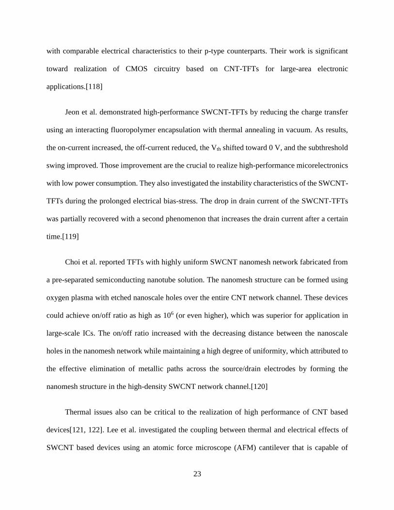
Figure 2.5 (a) Characterization of the self-aligned T-shape gate transistors based on aligned
polyfluorene-sorted CNTs. (b) Comparison of the RF performance between different CNT based
transistors. The extrinsic frequency response (left). The intrinsic frequency response with the
device de-embedding structure (middle). The intrinsic frequency response with the intrinsic de-
embedding structure (right) [186]. Copyright (2016) ACS Publications. .................................... 33
Figure 3.1 Fabrication of CNT-TFTs. (a) ~ (f) Fabrication process. (g) The sectional view of the
CNT-TFT. (h) CNT-TFTs fabricated in IEN cleanroom. ............................................................. 40
Figure 3.2 I-V characteristics. The overall I-V characteristics shows good performance of the p-
type CNT-TFTs with on/off ratio as high as 105 and mobility around 1-4 cm2 V-1 s-1. ................ 41
Figure 3.3 Statistics of CNT length distribution using Auto CAD software and a SEM image of
low-density CNT network. The white frame is selected randomly. The green splines denote CNTs

XII
that will be recorded (the red ones will not be recorded). The scale bar is used as calibration
standard in order to calculate the real lengths of all the target CNTs. .......................................... 43
Figure 3.4 Estimation of CNT network density based on image processing by converting the SEM
image into a binary image. The inset of the sample image is used to estimate the average diameter
of all the CNTs in the target image. .............................................................................................. 44
Figure 3.5 Measured output characteristics of fabricated CNT-TFTs. All devices are shown
together in (a), and shown separately for 5µm series (b), 10µm series (c), and 50µm series (d).
Green curves in (b)~(d) denote average output characteristics..................................................... 49
Figure 3.6 Id(sat) distribution for various channel lengths. L series: red=5µm series; blue=10µm
series, black=50µm series. Green stars denote average values for each series. ........................... 52
Figure 3.7 Schematic of output characteristics for S-CNT, M-CNT, and considering mutual
influence from both. ...................................................................................................................... 52
Figure 3.8 CNT length distribution from measurement. A sample of 300 CNTs was chosen for
statistics (x-axis). Green line denotes the average length (1.08µm) of the 300 CNTs (reference
average length ~1µm). .................................................................................................................. 52
Figure 3.9 Measured transfer characteristics using semi-log scale (a) and linear scale (b). of CNT-
TFTs for 5µm series (c), 10µm series (d), and 50µm series (e). Green curves in (a)~(b) denote the
average transfer characteristics. Green lines in (c)~(e) denote Vth extrapolation. The resulting Vth
distribution is shown in (f) for different L series. ......................................................................... 54
Figure 3.10 The variability based on the normal distributions of Vth ........................................... 55

XIII
Figure 3.11 The variability based on the normal distributions of CNT network density. ............ 56
Figure 3.12 (a) CNT length distribution. (b) Ls distribution for individual TFTs of each series. The
green line denotes the average Ls of all series. (c) The variability based on Ls. ......................... 58
Figure 3.13 The variability after considering comprehensive effect of Vth, ρ, and Ls. ................ 59
Figure 3.14 Comparison of variation range of different sources (Vth, ρ, and Ls) individually,
comprehensive effect of the three sources, and experimental measurement (without M-CNT effect)
for three different series (L=5µm, 10µm, and 50µm ) analyzed in previous sections. ................. 60
Figure 4.1 Schematic diagram of the experiment setup for gas sensing ....................................... 63
Figure 4.2 2-cycle (2ppm and 40ppm) sensor response under NH3 or NO2 spray for a long channel
TFT (2K: W=100µm/L=80µm) and a short-channel TFT (2H: W=100µm/L=8µm). Ro is the stable
device resistance before gas spray. (a)-(b) Sensor response of 2K under NH3 or NO2 spray
respectively. (c)-(d) Sensor response of 2H under NH3 or NO2 spray respectively. Inset figures are
the corresponding TFTs. Red curves are the fitting results using common time constants of double
exponential-convolution model. ................................................................................................... 64
Figure 4.3 Fitting for sensor response curves. (a) Linear transformation before fitting to standardize
the fitting process for different sensing gas. (b)-(c) Fitting result comparison of device 2H in gas
on and off state between double exponential-convolution (double exp) model, double t
exponential-convolution (double t exp) model, and quadratic model. (d)-(e) Fitting result
comparison of device 2K in gas on and off state between double exponential and double t
exponential models. ...................................................................................................................... 68

XIV
Figure 4.4 4-cycle (2ppm, 10ppm, 20ppm, 40ppm) sensor response and the corresponding fitting,
using common time constants of double exponential-convolution model at different gas
concentration. (a)-(b) Results for a long channel device 3F. (c)-(d) Results for a short channel
device 3A. ..................................................................................................................................... 70
Figure 4.5 4-cycle sensor response under NO2 spray and the corresponding fitting using common
time constants of double exponential-convolution model with different flowrates (600sccm,
800sccm, 1000sccm, 1200sccm) but at the same concentration of 50ppm. ................................. 71
Figure 4.6 Gas identification based on common time constant and the corresponding error
difference. (a) Fitting results from different gas assumptions (time constant pairs) for device 2K in
gas on state. (b) Same strategy as (a) for device 2K in gas off state. ........................................... 72
Figure 4.7 The cycling sensing experiment and comparison of the corresponding sensor responses
under NO2 spray at the same concentration (20ppm) for the same device at 5 hours’ time period.
Fitting 1 is based on common time constants and fitting 2 is based on separate time constants. . 73
Figure 4.8 One-to-one mapping for time constant pairs (τa ,τb) in gas on state (a) and gas off state
(b). The same marks denote the same gas type, and the same colors represent the same device. 75
Figure 5.1 Schematic of fabrication process of fully printed CNT-TFTs on flexible substrates using
AJP. (a) A well prepared flexible substrate (either Kapton or LCP) which is cleaned by 3-5min
oxygen plasma before printing. (b) Ag printing as S/D electrodes. (c) 1min oxygen plasma before
CNT printing for better wetting. (d) CNT network printing using a multiple layer by layer printing
method. (e) Dielectric layer/xdi-dcs printing. (f) 2-3min oxygen plasma treatment before Ag
printing. (g) Ag printing as a top gate electrode. A fully printed CNT-TFT is fabricated by this

XV
process. Note: Ag is cured at 150°C for 15~25min. Dielectric layer/xdi-dcs is cured at 140°C for
20min. ........................................................................................................................................... 78
Figure 5.2 Features and morphology of printed CNT-TFTs. (a) Fully printed CNT-TFTs on Kapton
substrate based on xdi-dcs layer. xdi-dcs layer is a transparent thin film under microscope where
CNT network (denoted by red dash box) is almost invisible in the channel. (b) Morphology of Ag,
CNT network, and a CNT-TFT using SEM. (c) Printed CNT-TFTs on LCP substrate based on
ALD dielectric layer. .................................................................................................................... 82
Figure 5.3 The effects of oxygen plasma treatment before CNT network printing (a)-(f) and Ag
printing on top of xdi-dcs thin film (g)-(h). Without plasma treatment, CNTs bundle together easily
(a)-(b) and Ag thin film is uneven with huge pinholes everywhere (g). CNT network density can
be well controlled by multiple layer by layer deposition after plasma treatment (c)-(f). Scale bar is
2μm in each figure. ....................................................................................................................... 83
Figure 5.4 I-V characteristics of CNT-TFTs. Transfer curve (a) and output curve (b) of printed
CNT-TFTs where gate dielectric were fabricated using ALD (~80nm Al2O3, W=500μm,
L=100μm, 1-cycle CNT network deposition). Transfer curve (c) and output curve (d) of a fully
printed CNT-TFTs based on printed dielectric layer with thickness as small as 0.3μm (W=500μm,
L=100μm, 3-cycle CNT network deposition). .............................................................................. 84
Figure 5.5 The impact of the printed xdi-dcs layer on the performance of fully printed CNT-TFTs.
(a) Comparison of transfer curves of four fully printed CNT-TFTs with different thickness of
dielectric layers. (b) The dependence of Vth on the thickness of printed xdi-dcs thin films for fully
printed CNT-TFTs. ....................................................................................................................... 86

XVI
Figure 5.6 (a) Schematic structure (layer by layer structure and the sectional view) used to test the
insulation quality of printed xdi-dcs thin films. (b) Visualization of printed xdi-dcs thin film at
different dilute ratio σ and UA. The devices in upper figures will not work as numerous pinholes
created during xdi-dcs printing. The middle figures show well printed xdi-dcs thin films. The lower
figures will not work either because of the over printing, which can result in several big pinholes
(denoted by red dash area, left) and even ruin the substrate (right). ............................................. 88
Figure 5.7 Optimization of printed xdi-dcs thin film. (a) Yield rate (number of samples with good
insulation quality) under different σ and UA combinations. (b) Thickness dependence of xdi-dcs
thin film on UA when σ equals to 1:2.5, which is the best σ from (a). The black dash box in (a)
and (b) denotes UA range of 30-38CCM at best σ. ...................................................................... 90
Figure 6.1 Fabrication steps of AJP sensors (a) and highly simplified fabrication steps of IJP
sensors (b). For IJP, extremely low-cost daily-used printers (Epson C88+ or Artisan 1430) were
utilized without any controllable stage. ........................................................................................ 94
Figure 6.2 Morphology and comparison of CNT sensors fabricated by AJP on Kapton substrate
(a), IJP on PET substrate (b), and PL on Si wafer (c). SEM was used for the imaging of CNT
network and Ag electrodes. Uniform CNT network was obtained in both PL and AJP process, but
severe CNT bundling effect was observed in IJP process. CNT network is invisible under low
resolution microscope. .................................................................................................................. 96
Figure 6.3 Schematic of the experimental setup for gas sensing .................................................. 97
Figure 6.4 Sensor responses of AJP sensors (a-b), IJP sensors (c-d), and PL sensors (e-f) under
~10min NO2 spray (orange strips) and 10min NH3 spray (green strips) at 2ppm and 20ppm

XVII
concentration. Color strips denote gas on states (orange for NO2 and green for NH3), no strip
denotes gas off state. The width of each color strip denotes the length of 10min. (g) sensitivity
error bars of the PL, AJP, and IJP sensors. ................................................................................... 98
Figure 6.5 Variabilities in response of sensors, printed by AJP, with respect to different CNT
network: layer by layer printed uniform CNT network (with oxygen plasma treatment) (a), drop-
cast CNT network with CNT bundling effect (no surface treatment involved) (b). The inset figures
are SEM imaging of CNT network patterned by the two different methods. ............................... 99
Figure 6.6 Comparison of sensitivity distribution of AJP sensors with respect to different CNT
network: printed uniform CNT network (with oxygen plasma treatment, stars), drop-cast CNT
network with severe CNT bundling effect (no surface treatment involved, triangles). .............. 103
Figure 6.7 Sensitivity improvement of an IJP sensor under NH3 spray at 2ppm and 20ppm. Black
curve is the sensor response from the original IJP sensor with relatively low sensitivity. Red curve
is the improved sensor response of the IJP sensor with post drop-cast CNT deposition. The SEM
images show the change of CNT network after post drop-cast deposition. ................................ 104
Figure 7.1 Sensor responses of mixed gases. Same concentration of NH3 at 5ppm (a) and 40ppm
(b) with increasing concentration of NO2 for each cycle. ........................................................... 112

XVIII
LIST OF SYMBOLS AND ABBREVIATIONS
Abbreviations
abs Absolute value
AFM Atomic force microscope
AJ200 The aerosol jet 200 system
AJP Aerosol jet printing
ALD Atomic layer deposition
AMECD Active-matrix electrochromic display
AMOLED Active matrix organic light-emitting diode
As_white White pixel area in the sample binary image
At Total area of the target SEM image
At_white White pixel area in the target binary image
ChemFET Chemical field-effect transistor
CMOS Complementary metal–oxide–semiconductor
CNT Carbon nanotube

XIX
CNT-FET Carbon nanotube field-effect transistor
CNT-TFT Carbon nanotube thin film transistor
cP Unit of centipoise
CVD Chemical vapor deposition
DI Deionized (water)
Ds_CNT Average CNT diameter in the sample binary image
Dt_CNT Average CNT diameter in the target binary image
FET Field-effect transistor
G Gate electrodes
GND Grounded
h Height of the pulse signal in a sensing cycle
IC Integrated circuit
Id Drain current
Id(sat) Saturated drain current
IEN Institute for Electronics and Nanotechnology
IJP Inkjet printing
IPA Isopropyl alcohol

XX
L Channel length
LCP Liquid crystal polymer
Ls The mean length of CNTs
Ls_CNT Total CNT length in the sample binary image
Lt_CNT Total CNT length in the target binary image
m A universal exponent of CNT percolating system
MOS Metal-oxide-semiconductor
MOSFET Metal-oxide-semiconductor field-effect transistor
MWCNT Multi-walled carbon nanotube
M-CNT Metallic carbon nanotube
NAND A digital logic NAND gate
nIR Near-infrared
NOR A digital logic NOR gate
PDF Probability distribution function
PDMS Polydimethylsiloxane
PEI Poly (ethylene imine)
PET Poly(ethylene terephthalate)

XXI
PL Photolithography
PR Photoresist
PS Printing speed
PVD Physical vapor deposition
PVP/PMSSQ Poly(vinylphenol)/poly(methyl silsesquioxane)
R Resistance of a CNT device over time
Rc Contact resistance between CNTs and electrodes
RF Radio frequency
RFID Radiofrequency identification
RIE Reactive-ion etching
Rm Maximum or minimum resistance of a sensor in a sensing cycle
Ro Stable resistance of a CNT device before gas spray
RSD Total resistance of random CNT network in the channel
S Sensitivity of a sensor
SEM Scanning electron microscope
SG Sheath gas flow rate
SMUs Source measurement units

XXII
SRAM Static random-access memory
SWCNT Single-walled carbon nanotube
S/D Source and drain electrodes
S-CNT Semiconducting carbon nanotube
t Time
TEM Transmission electron microscope
TFT Thin film transistor
TLM Transfer length method
to Time of onset point in a sensing cycle
UA Ultrasonic atomizer flow rate
UHV Ultrahigh vacuum
Vdd Supply voltage
Vds Drain voltage
Vgs Gate voltage
Vth Threshold voltage
W Channel width
xdi-dcs Dielectric ink: a blend of PVP/PMSSQ solution

XXIII
ξ A function of the geometrical parameters and bias conditions
λ Standard deviation in a distribution function
σ Volumetric dilute ratio
ρ CNT network density
τa Time constant in a convolution model
τb Time constant in a convolution model
μ Statistical mean value in a distribution function
υ Standard deviation for error evaluation

XXIV
SUMMARY
Single-walled carbon nanotubes (CNTs) are promising candidates for future electronic
devices because of their excellent electrical, mechanical, optical and chemical properties. CNT
based sensors have high potential for large scale adaptation because of its high sensitivity, fast
response, and physical/chemical stability. Fabrication of CNT based devices such as thin film
transistors (TFTs) by photolithography (PL) can reach high resolution, and meet the requirements
of aggressive scaling of physical dimensions like Si-based metal-oxide-semiconductor field-effect
transistors (MOSFETs). However, the complicated processes and need of expensive equipment of
PL become a major drawback and severely limits its application in various fields. Fully printed
CNT-TFTs, using inkjet (IJP) or aerosol jet (AJP) printing, possess tremendous advantages in
design versatility and operational customization for sensing devices. They are also very promising
for cost-effective and scalable production of flexible/wearable devices. However, the performance
of CNT-TFTs and their usage as CNT sensors need to be significantly improved.
For CNT-TFTs fabricated by PL, device-to-device performance variability can pose
challenging problems for its practical applications. To address this issue, both experimental and
theoretical methods were employed to analyze the variability in I–V characteristics in a statistical
framework. For the experimental analysis, array of CNT-TFTs were fabricated with high-k
dielectric HfO2 as gate oxide layer to achieve high performance. For the theoretical part, the current
scaling relationship was applied to analyze variation sources such as % of metallic CNTs (M-
CNTs), threshold voltage, CNT mean length, etc. Results show that a better consistency in
performance can be guaranteed for TFTs with larger channel area, which ensures a smaller
variation in CNT network density and CNT mean length. The fabricated CNT-TFTs can be used
XXV
as gas sensors for ammonia and nitrogen dioxide detection at low ppm concentrations. To improve
the selectivity of CNT sensors, a double exponential-convolution model was developed to decipher
sensor response as well as to explore its application in gas identification. The uniqueness of time
constants of the model can work as identity verification for different sensing gases, which
demonstrates that the sensor response is a distinctive behavior determined by the unique channel
structure of each TFT.
For fully printed CNT-TFTs, the performance is mainly limited by the printed gate
dielectric. Its relatively large thickness can result in high gate voltage to switch on and off the
transistors, which will cause high power dissipation for printed devices. In response to address this
challenge, fully printed CNT-TFTs have been fabricated on flexible substrates using AJP. The
devices show very stable performance including high on/off ratio, high mobility, negligible
hysteresis, and good uniformity. More importantly, these devices can be operated using bias
voltages as small as ±5V, which is much smaller than the previously reported values and is a
consequence of the improvement in printing both CNT network and gate dielectric layer. The fully
printed CNT sensors are also fabricated using AJP or IJP separately. Compared to PL, printed
sensors show no degradation with respect to sensitivity and stability, but can be fabricated at much
lower cost. Besides, the sensitivity of printed CNT sensors can be highly improved using post
drop-cast CNT deposition without any surface functionalization. This work provides key insights
for the fabrication and usage of extremely low-cost CNT gas sensors, which has immense potential
in flexible and wearable devices as well as air quality detection and industrial emission control.

1
CHAPTER 1. INTRODUCTION
Carbon nanotubes (CNTs) are one-dimensional cylinders of monolayer graphene which is
made of carbon atoms arranged in a hexagonal / honeycomb structure with open or close ends. It
is a promising candidate for future nanoscale devices[1]. Diameters of CNTs can range between
0.8 nm to 20 nm and their lengths can be as large as several centimeters. The advantages of the
CNT mainly lie in its remarkable properties such as high carrier mobility, excellent thermal
conductivity, high mechanical flexibility, and high photo transparency, etc. Field-effect transistors
(FETs) are the most common type of transistors, which are the basic building blocks used in
amplifiers, switches as well as logic, memory, and sensors [2-4]. The structure of a typical CNT-
FET with randomly distributed CNT network is illustrated in Figure 1.1. Other CNT-FETs with
single CNT and aligned CNT network in the channel are also extensively used in different
applications. The unique properties make CNTs, especially single-wall carbon nanotubes
(SWCNTs) a perfect material for transistors.
Figure 1.1 Schematic of a CNT-TFT with randomly distributed CNT network. W is channel
width, L is channel length, Vds is drain voltage, Vgs is gate voltage, and GND is grounded.
2
1.1 Progress in CNT based Devices
Ever since Gordon E. Moore made a prediction on doubling the number of transistors on IC
every two years, the semiconductor industry has been driven to reach this goal mostly by scaling
down the size of transistors [5]. The projection has been achieved when the device dimension was
reduced to sub-22nm. At this level, the steady growth of transistor numbers started to slow down
due to limitations from both miniaturization and device performance. The deceased size problems
will cause short channel effect, current leakage, and power dissipation[6-8].
Figure 1.2 Structure and performance of 10-nm CNT based complementary metal-oxide
semiconductor (CMOS) FETs [9]. (a) The cross sections of a p-type FET, n-type FET, and
gate stack; gate length 10 nm, channel length 20 nm. (b) Transfer characteristics of typical
CMOS FETs fabricated on a s-SWCNT with a diameter of 1.3 nm at a drain bias Vds = ±0.4
V. The solid blue and green curves represent CNT p-type and n-type FETs, respectively. (c
and d) Comparison of 10-nm CNT CMOS FETs and commercial Si CMOS transistors of
Intel’s 14-nm (22) (solid black curve) and 22-nm nodes (23) (solid maroon curve). The on
currents of n-FETs for CNT, Si 14-nm node, and Si 22-nm node are 1.16 mA/mm (supply
voltage Vdd = 0.4 V, 125 CNTs/mm), 1.1 mA/mm (Vdd = 0.7 V), and 1.03mA/mm (Vdd = 0.8
V), respectively. The on-currents of p-FETs for CNT, Si 14-nm node, and Si 22-nm node are
0.76 mA/mm (Vdd = 0.4 V, 125 CNTs/mm), 0.96 mA/mm (Vdd = 0.7 V), and 0.83mA/mm (Vdd
= 0.8 V), respectively. CNT CMOS FETs and 14- and 22-nm Si CMOS FETs have gate
lengths of 10 nm, 20 nm, and 26 to 30 nm, respectively. Copyright (2017) American
Association for the Advancement of Science.

3
CNT-FETs are one of the promising alternatives for further miniaturization and they have
been widely researched. Even though good progresses have been made, their high application
potential still needs to be exploited to take the place of conventional metal-oxide-semiconductor
field-effect transistors (MOSFETs) in the future. As a new generation of transistors, CNT-FETs
have significant advantages such as low power consumption, high flexibility, and high operation
speed [9, 10]. CNT-TFTs are also promising for flexible microelectronic applications because of
their high mobility, substrate-neutrality, and low-temperature fabrication process. These
capabilities enable a wide range of applications such as wearable/flexible e-displays, disposable
electronics, chemical/biological sensors, etc. [3, 11-19]
Figure 1.2 shows the transmission electron microscope (TEM) images of the cross sections
of CNT-FETs (with gate length 10 nm and channel length 20 nm; the smallest size can reach 5
nm) and the performance comparison with transistors fabricated by Intel. It turned out that the
performance of CNT-FETs is better than silicon complementary metal-oxide semiconductor
(CMOS) FETs at the same scale. The 5 nm CNT-FETs actually approached the quantum limit of
FETs by using only one electron per switching operation.
Most of these advantages root in the excellent performance of CNTs, which can be classified
as either single-walled (SWCNT) or multi-walled carbon nanotube (MWCNT). As a one-
dimensional nanoscale material, individual CNTs exhibit exceptional electrical, mechanical,
chemical, thermal, and optical properties. SWCNTs have exceptional high current carrying
capacity as its mobility can reach as high as 100,000 cm2 V-1 s-1 [10, 20]. Extraordinary flexibility
and elasticity can also be expected when it undergoes high strain and bending. Aligned SWCNT
based thin film transistors (TFTs) have certain advantages such as small TFT dimensions, high
mobility, and only few CNTs are needed per channel. The CNT network based TFT is also of high
4
interest for low-cost and large area electronic applications such as antennae, RF tags, sensors, etc.
as it is much easier to fabricate on both flexible and hard substrates [21, 22]. In recent years, the
cost of CNTs has significantly dropped and the large amount of CNT usage per TFT is not
necessarily a major concern from a cost standpoint.
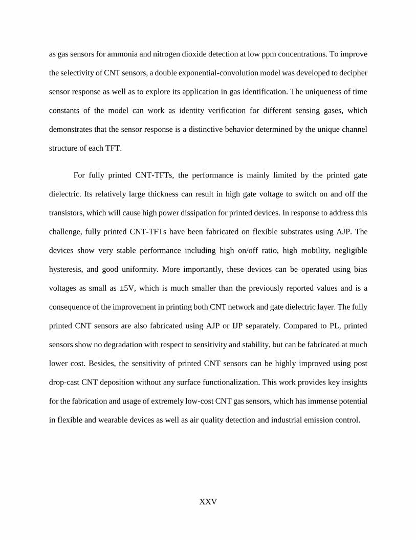
Figure 1.3 presents one of the applications in three-dimensional flexible CMOS logic circuits
[22]. These flexible SWCNT-TFT CMOS circuits have a 3D structure based on a two-layer stack
of SWCNT networks. Other 3D flexible circuits such as CMOS NOR, NAND logic gates, and 15-
stage ring oscillators were fabricated on the same polyimide substrates with high performance as
well, which also showed stable electrical properties with bending radii as small as 3.16mm. It
demonstrates this 3D structure is a reliable architecture and suitable for carbon nanotube electrical
applications in complex flexible and wearable electronic devices.
Figure 1.3 (a) Schematic of 3D flexible CMOS CNT-TFT inverter. (b) Optical microscope
photo of the two nested 3D CMOS ring oscillators. (c) Optical images of 3D flexible CMOS
inverter arrays based on CNT-TFTs formed on polyimide substrate [22]. Copyright (2016)
ACS Publications.

5
The sensitivity of CNTs has been utilized in sensor applications because of its unique
structure for high sensitivity. As sensor material, CNTs have large surface area and exhibit charge-
sensitive conductance, which attributes to the carbon atoms and C-C bonds on the tube surface
[23]. The conductance of CNTs is known to be sensitive to ambient environment, especially to
oxygen and oxygen-containing gaseous species [24, 25]. In addition, CNT sensors can also work
for the detection of hydrogen (H2) [26, 27], organic vapors [28], alcohols [29], protein [30], etc.
which has huge practical significance for disease and health diagnosis [31-33]. CNT based sensors
can also benefit from their low cost, room temperature operation, and nanoscale and
microelectronics applications [10, 34, 35].
Figure 1.4 Detection of protein from crude cell lysate and from Escherichia coli (E. coli)
(bacteria) engineered to secrete target protein [30]. (a) Concentration–response curves for
0 (cyan), 1 × 10⁸ (orange), 4 × 10⁸ (blue), 7 × 10⁸ (red), 1 × 10⁹ (green) and 1.6 × 10⁹ (black)
c.f.u. ml−1 E. coli. (b) Two representative single-sensor fluorescence intensity traces (red and
blue) for an agarose gel-immobilized E. coli bacterium. Copyright (2017) Nature Publishing
Group.

6
Figure 1.4 plots the detection of protein efflux from microorganisms using fluorescent
SWCNT based sensor arrays. Protein binding to aptamer targets on SWCNTs subsequently relays
an optical signal in the near-infrared (nIR) optical window. And SWCNTs are the only
fluorophores to date that have essentially infinite lifetimes and are not susceptible to on–off
blinking, as quantum dots are. Therefore, the signal produced by SWCNTs, combined with the
selectivity provided by aptamers, provides much promise for the long-term optical monitoring of
specific protein targets from within crude biological samples over long timescales [30]. As
nanosensor arrays, which can provide a distinct way to achieve ultralow detection limits in solution
by proximity placement to an analyte, they enable real-time, single-cell analysis of different
protein products from various cells.
1.2 Motivation and Challenges
1.2.1 Fabrication
Figure 1.5 The aerosol jet process provides a cost-effective solution for low to moderate
volume production runs or where mass customization is required. The cost per unit for
printing techniques is flat regardless of volume (copyright belongs to Optomec Inc).

7
Even though advances in high resolution lithography process (and other traditional
fabrication methods) have achieved smallest features of several nanometers for CNT based devices
which almost approaches the quantum limit, the corresponding high cost has severely limited their
further applications. The improvement of printing techniques, synthesis, and processing of
nanomaterials has brought fresh impetus to the development of printed flexible devices[36]. First,
printing techniques such as AJP and IJP can reach spatial resolution as small as ~20 µm and this
spatial resolution can be further decreased in the near future. Even though they cannot compete
with traditional fabrication methods in resolution, they are good enough for applications in most
flexible and wearable electronics. Secondly, printing techniques have much simpler fabrication
process, which do not involve too many other high-cost equipment or complicated procedures.
Thus, the overall cost is much lower and it can save time when making a prototype. Moreover,
incredibly resource-efficiency is also one of their major advantages because printing techniques
apply the so-called “additive” process instead of a traditional “subtractive” process, which
produces much less waste than traditional fabrication methods. Besides, printing techniques are
also very suitable for large-scale production, etc. Figure 1.5 compares the cost between AJP
printing and typical traditional fabrication methods.
However, the tradeoff between cost and performance is still an urgent problem to be solved
because of the huge gap between printing techniques and traditional fabrication methods. It is
becoming quite critical to fabricate microelectronics using printing techniques for cost
consideration while maintain the relatively high performance and stability at the same time, which
has significant potential in applications of flexible electronics.
8
1.2.2 Performance Variability
Even for devices fabricated using the PL process, device-to-device performance variation of
CNT-TFTs is becoming a critical problem while trying to harvest the exceptional properties of
CNTs. Performance variations of TFTs can be reflected in the variability in I-V characteristics,
including output and transfer characteristics. It results from the multiple sources. The atomic
structure of CNT is a source of large variation, which includes variations in diameter, defects,
doping, length, etc. A CNT of similar diameter can be either metallic or semiconducting depending
on its chirality, leading to significant variability in I-V characteristics. The CNT network
distribution and morphology in its channel area, e.g., CNT network density, channel length, and
orientation, are very different from one TFT to another because of the randomness induced during
deposition. Fabrication process, especially fabrication imperfections, further affects the variability.
Even though the CNTs are grown by the same method and the devices are fabricated under the
same processing conditions, the I-V characteristics of TFTs can still vary.
In the previous studies, performance variation of CNT-FETs had been discussed with respect
to the CNT diameter, CNT density fluctuation, CNT growth and manufacturing process. Cao et al.
studied variability in threshold voltage (Vth) of CNT-FETs. It showed that variability in Vth mainly
results from the random fluctuation of fixed charges on the oxide/air interface [37, 38]. Franklin
et al. analyzed the origin of variability in Vth and hysteresis of CNT-FETs, and tried to improve
the device-to-device consistency through optimized gate dielectric and passivation layer [39].
However, most of the studies only focused on the devices using single or aligned nanotubes as
channel. Performance variability of FETs with aligned CNTs [40-42] is of high interest because
of large variation in FET performance with small changes in CNT structure, which had been
studied to achieve better consistency. None of the previous studies reported the variability analysis

9
of CNT-TFTs using random CNT networks as channel. For CNT networks, the variability analysis
becomes more complicated due to randomness in the network structure and CNT distribution,
which varies with respect to CNT network density, deposition methods, surface condition before
CNT deposition, etc. Undoubtedly, these further increase performance uncertainty which need to
be analyzed and understood thoroughly.
1.2.3 Chemical Sensors
SWCNT based chemiresistor gas sensors have been widely studied due to their significant
advantages in monitoring different gases in low ppm and ppb level. The first CNT gas sensor was
reported in 2000 by Kong et al. [43] Since then, many research groups have worked on the sensor
application and enormous progress has been achieved. Reports on the sensing mechanism have
been discussed and argued still today. Early discussions mainly focused on the adsorption of gas
molecules at CNT junction area [44], indirect interaction through pre-adsorbed water layer or the
hydroxyl group from SiO2 substrate [45, 46], direct charge transfer between gas molecules and
CNT [47], and Schottky barrier modulation at the CNT/metal contacts [23], etc. Battie et al.
performed an experiment based on CNT network and suggested gas molecules mainly attach to
CNT network, not CNT/metal contacts [48]. Later, Boyd et al. pointed out the gas sensitivity is
due to both the CNT/metal contacts and the CNT junctions [49], and the network effects are
dominated by gas-induced changes in CNT junctions. As for sensitivity, a detection limit of 3ppb
ammonia (NH3) was demonstrated by Rigoni et al [50].
Functionalization strategies, including polymers coating or CNT decoration with different
metal nanoparticle, were performed and yielded good results. But these methods degraded the
overall performance of the sensors in terms of response rate and long-term stability. Random CNT

10
network and aligned CNT network in sensors were also investigated with single decorated
molecules and nanoparticles, either in chambers or in air. However, few researches focused on the
selectivity of CNT based gas sensors, and no publication has been reported on gas identification
study without functionalization or coating or using array of CNTs. More work needs to be done to
explore the selectivity of CNT sensors.
1.2.4 Flexible Electronics and Sensors
Printed microelectronics on flexible substrates has attracted significant attentions in recent
years because of the high potential in wearable and bendable devices[21]. Its applications include
flexible displays[51], radiofrequency identification (RFID) antennae/tags[52, 53], sensors[54, 55],
artificial skins[56], etc[57]. As for printing techniques, AJP has been proven to be capable of
printing microelectronic devices and relevant circuits with low-cost, repeatability, scalability, and
relatively high precision compared to other printing techniques[58]. AJP has been utilized to
deposit a wide range of materials because it can handle inks viscosities in the range of 1-1000
Cp[59] Printed CNT-TFTs have significant potential with improved carrier mobility, device
stability, variability, dissipation power, and other operation performance[60-62].
Even though advances in printing techniques, synthesis and processing of nanomaterials
have promoted the development of printed flexible devices[36], the tradeoff between cost and
performance still limits their further applications in various fields. On the one hand, fully printed
CNT-TFTs are crucial for low-cost consideration. Procedures such as atomic layer deposition
(ALD) will complicate the process and increase the cost at the same time. On the other hand, high
performance is hard to achieve for fully printed CNT-TFTs. The causes are different, such as
imperfections in electrode patterns, contact interfaces, uniformity of CNT network, thickness of

11
dielectric layer, etc[11]. Most of them are being addressed properly with the improvement of
nanomaterial inks, including nanoparticle silver (Ag) inks [63], highly purified semiconducting
CNT (S-CNT) inks [64], ion-gels [65, 66], dielectric inks such as barium titanate (BaTiO3)
nanoparticles[67] and xdi-dcs [68], which is a blend of poly(vinylphenol)/poly(methyl
silsesquioxane) (PVP/pMSSQ). However, printable dielectric layer is still one of the major
obstacles because its relatively large thickness can result in very high gate voltage to fully switch
on and off the transistors, which will cause high power dissipation for printed devices on flexible
substrates. For example, the high Vth in some fully printed TFTs highly limited their performance
because the gate bias has to be as large as ±40V to fully switch on/off the transistors. Ion gel could
be an alternative solution to address the specific problem of high Vth [65, 66, 69], but it is
temperature sensitive, very fragile and unstable compared to other dielectric materials. In this
context, the optimization of fully printed CNT-TFTs, especially the printed CNT network and
dielectric layers, is becoming more and more indispensable to make full use of its high potential
in many practical applications.
1.3 Scope of Current Work
The proposed research tasks are organized in the following sequence. Chapter 2 summarizes
the literature for CNT–TFTs, including their excellent properties, fabrication processes, and
various applications. It also lists the important contributions of the present work. Chapter 3
concentrates on the fabrication of CNT-TFTs by typical PL process and discusses the performance
variability in output characteristics of the fabricated CNT-TFTs. Chapter 4 presents CNT-TFTs’
application as selective chemiresistor sensors for gas identification by putting forward a
convolution model to characterize the corresponding sensor responses. Chapter 5 discusses the
improvement in device performance after the optimization of fully printed CNT-TFTs using AJP,

12
including the printed CNT network and dielectric thin film. Chapter 6 characterizes the sensor
responses of fully printed CNT sensors fabricated by different printing techniques as well as puts
forward an efficient strategy to improve the sensitivity. Chapter 7 summarizes the current work
and introduces the scope of future work.

13
CHAPTER 2. BACKGROUND
2.1 CNTs and CNT Based Devices
2.1.1 Properties of CNTs
Since their discovery in 1991, CNTs have become one of the most highly researched
materials in the areas of science and engineering due to their superior electrical, mechanical,
chemical, thermal, and optical properties[70]. CNTs can be classified as either MWCNTs or
SWCNTs. SWCNTs can be further classified as either metallic (M-CNTs) or S-CNTs[71].
Electrical Properties
For a SWCNT, the mobility and current carrying capacity can be exceptionally high [72].
Nevertheless, large difference exists between properties of M-CNTs and S-CNTs. Because 1/3rd
of SWCNTs are metallic in a grown CNT network, a significant variation in property among CNTs
is not unexpected. S-CNTs show stronger temperature dependence than M-CNTs in conductivity
due to the thermal excitation of carriers[73]. For CNT thin film, which contains both M-CNTs
and S-CNTs, carrier transport includes travelling across tube-tube junction in addition to merely
along the tube. The M-M or S-S CNT junctions have 20kΩ~400kΩ contact resistance, but M-S
contact resistance is found to be as high as 1MΩ~5MΩ. Hence, the CNT-CNT contact resistance
is one of the main contributions to the film resistance and network transport properties.
Mechanical Properties
CNTs show extraordinary mechanical flexibility and elasticity when they undergo large
strain and bending [74, 75]. This can be credited to the large aspect ratio and strong internal

14
bonding within CNTs. Defects may be introduced upon deformation, and they will affect both
electrical and thermal transport properties. Therefore, the superior mechanical property of
individual CNTs is an important figure of merit. Moreover, because of the strong interaction
between substrate and CNTs, CNT thin films are amazingly flexible, stretchable, and foldable
without causing significant reliability problem. Typically, a CNT thin film can be bent down to
radius of 2 mm without causing damage to network.
Chemical Properties
Because of the special structure of CNT where all carbon atom and C-C bonds are on the
tube surface, the chemical sensitivity of CNTs can be utilized in sensing applications [76]. After
absorbing chemicals, two resulting effects may be observed. One is the change in carrier
concentration due to charge transfer between CNTs and incoming chemicals. The other is the
induced potential energy barrier that affects carrier mobility along the tube. CNT thin films are
required to have an acceptable chemical stability after exposure, especially to those chemicals that
will be employed in fabrication and regular usage.
Thermal Properties
The thermal conductivity of a SWCNT can reach 3500W·m−1·K−1 along its axis at room
temperature, which is much higher than the widely used high conductivity metal copper (385
W·m−1·K−1). CNTs can also bear high temperature in practice. The temperature stability of CNTs
is estimated to be up to 750°C in air and about 2800°C in vacuum [75]. Crystallographic defects
strongly affect CNTs’ thermal properties, which leads to phonon scattering and in turn increases
the relaxation rate of the phonons, thus reducing the thermal conductivity. Besides that, CNTs also

15
show superior optical properties and CNT network is relatively easy to deposit by multiple
methods for the fabrication of TFTs.
2.1.2 CNT Network
The most common technique to grow CNT network or CNT thin films is chemical vapor
deposition (CVD) [77]. CVD has a great advance in density control by tuning the catalyst density
and growth time. It also gives a better tube-tube contact and fewer defects that result in higher
conductance. However, solution-based deposition is more suitable for pressure and temperature
sensitive electronics [78]. It is also more compatible for fabrication of plastic/flexible electronic
devices. Compared to CVD, the cost of solution-based deposition is much lower since it operates
at low temperature and no vacuum system is needed. The highly purified S-CNT solution are
commercially available nowadays, which are typically either water based or solvent based.
Solution-based deposition further increases the design flexibility and makes it more accessible for
mass production of CNT based microelectronics/circuits.
Uniformity of CNT thin films is very important to obtain high performance [21, 79]. To
achieve this, the quality of CNT solution and coating methods are crucial. For example, the
“Langmuir-Blodgett” method spreads CNT solution over a substrate surface covered by a water
layer. Self-assembly method enhances the interaction between CNTs and deposition surface by
chemical treatment, local surface charge, or microfluidic guidance. For electrophoretic deposition,
a metallic layer is added on top of the substrate and CNTs are locally charged and polarized by an
electric field. After deposition, the conductive layer will be etched away, leaving only the
transparent CNT thin films. All these deposition methods can accommodate to various objectives.
2.1.3 CNT Based Thin Film Transistors
16
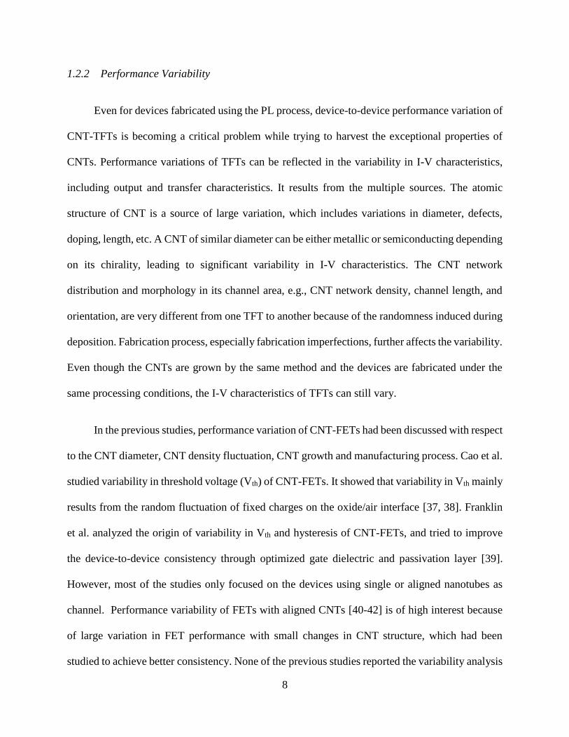
CNT-TFTs can withstand high degree of strain, exhibit excellent electrical performance due
to their high mobility, on/off ratio [80-82]. Even though individual CNT based FETs can meet the
requirements of aggressive scaling down of physical dimensions, they have been deemed
impractical for commercialization due to the difficulty of pinpointing individual CNTs at desired
locations and the performance variability depending on the chirality and diameter of individual
CNTs. CNT network based TFTs are more practical due to the ease of fabrication using either
conventional lithography or printing techniques, and their relatively high device-to-device
performance uniformity which is vital for scalable production.
Figure 2.1 Complementary SWCNT-TFT structures and performance. (a) Micrographs of
the fabricated SWCNT-TFT device with a channel width of 150 μm and length of 50 μm
(inset) and an array of SWCNT TFTs. (b) Time stability of SWCNT-TFT electrical
properties. Left: Log-linear transfer curves for encapsulated p-type (solid lines) and n-type
(dashed lines) SWCNT-TFTs measured after initial exposure to atmosphere (blue) and after
7 h of ambient exposure (green); Right: Log-linear transfer curves for unencapsulated p-
type (solid lines) and n-type (dashed lines) SWCNT TFTs measured after initial exposure to
atmosphere (blue) and after 5 h of atmospheric exposure (red), with the change in Ioff
indicated by the arrow (red/blue). Copyright (2015) Nature Publishing Group. [83]

17
Geier et al. fabricated both p-type and n-type SWCNT-TFTs using methods similar to a
previous work[84]; they modified the structure to encapsulate the doped SWCNT channel
networks. The schematic structure and corresponding performance are shown in Figure 2.1. Based
on these transistors, SWCNT CMOS static random-access memory (SRAM) cells and
corresponding circuits were also fabricated. Read, write, and hold noise margin stability testing
was obtained for these SWCNT CMOS SRAM cells over 40 h (4,000 cycles) of ambient testing
with high temporal stability and spatial uniformity. Overall, their work provides an approach for
the design and fabrication of complex solution-processable, large-area, energy-efficient CMOS
logic devices. These features have potentially wide-ranging implications for high-performance
wearable and bendable electronics when combined with recent advances in flexible and printed
electronics. [83]
CNT-TFTs on bendable substrate have attracted major interests because of their wide range
of applications in flexible electronics such as transparent displays, chemical/biological sensors,
RFIDs, logic circuits, oscillators, etc. [10]. The main advantages of the flexible TFTs lie in their
potential to enable low-cost, and high throughput manufacturing in practice. To further realize the
cost-effective and scalable production of flexible TFTs, printing techniques have been introduced
as a viable solution. Printable TFTs do not require fabrication masks or templates, which provide
significant design flexibility compared to the conventional photolithography (PL) process.
Feng et al. proposed artificial synapses based on dual-gate SWCNT-TFTs which are
fabricated by printing techniques[85]. High field-effect mobility was demonstrated for those
printed low-voltage synaptic devices. Some key synaptic behaviors were emulated including
paired-pulse facilitation and filtering characteristics. They presented a printable method to
fabricate synaptic devices for a neuromorphic system.

18
2.1.4 Hysteresis of CNT-TFTs
Hysteresis of transistors is highly undesirable in practice[86, 87]. Hysteresis can result from
various factors such as trap states in the dielectric or semiconductor/dielectric interface, trap
charges induced by water molecules absorbed onto or in the vicinity of the semiconductor channel.
Hysteresis can lead to a shift in Vth as a function of the voltage sweeping speed, sweeping direction,
and sweeping range. Instability and reliability problems can result from hysteresis during transistor
operation and logic circuit design [88-90].
Lee et al. studied gate hysteresis of CNT-FETs on silicon oxide substrates in an ultrahigh
vacuum (UHV) at low temperatures[87]. Results showed the hysteresis decreases greatly upon co-
adsorption of water and ammonia below condensation temperatures. But it is neither reduced by
thermal annealing over 300°C under UHV nor significantly affected by independent adsorption of
ammonia or water at 56 K. Yu et al. demonstrated transparent and flexible transistors and logic
gates using a monolayer graphene electrode and CNT network in the channel. Small hysteresis
was observed for the nanocarbon based integrated circuits (ICs) [91]. Because of the defect-free
graphene surface, the hysteresis of the devices was independent of the gate voltage sweeping range.
Ha et al. applied fluorocarbon polymer (Teflon-AF) in CNT-TFTs and obtained hysteresis-
free performance in the transfer characteristics[92]. This fluorocarbon encapsulation method
provides a promising approach for enhanced device stability and reliability, which is critical for
future CNT based system-level electronics. Cao et al. also reported hysteresis-free CNT-TFTs
using AJP techniques[68]. They fabricated fully printed transistors on flexible substrate (Kapton),
which includes the printing of all layers: S-CNTs, metallic electrodes, and insulating gate
dielectrics. Other hysteresis-free devices can be seen in [86, 93-98].

19
2.1.5 Variability Analysis of CNT-TFTs
Performance variability of transistors increases with the decrease of the smallest feature size,
resulting in large challenges in device reliability and stability. The challenges include the
unpredictability of delay to increasing leakage current, as well as the inherent unreliability of the
components, posing design, and test challenges[99].
Islam et al. discussed the variability and reliability of SWCNT-FETs in different
aspects[100]. They pointed out that performance variability of SWCNT-FETs is mainly attributed
to both the distributions of SWCNTs’ diameter and the interface defects caused by hydroxyl-
group. Besides, oxide defects also play a dominant role in controlling reliability parameters, like
low-frequency noise, radiation damage, and long-term performance degradation. Salamat et al.
explored the origin of large device-to-device fluctuation in aligned array transistors[101]. They
developed numerical simulations using measured diameter distribution of CNTs to demonstrate
that the diameter distribution had significant impacts on the variability. Results showed the control
over diameter distribution is vital for attaining high-performance transistors and circuits with
characteristics rivaling those of the state-of-the-art Si technology. Hu et al. presents variability and
reliability analysis of self-assembled CNT-FETs based on thousands (~3000) of multichannel
CNT-FETs [102]. By increasing the number of channels in CNT-FETs, the on-state current was
increased and the Vth was reduced. Moreover, the major failure mode in the scaled multichannel
CNT-FETs may be the “shorts” caused by M-CNTs. Almudéver et al. studied the variability and
reliability of CNT-FETs due to the density variations [39] and manufacturing imperfections[103],
including the presence of M-CNTs, imperfect M-CNT removal processes, chirality variations,
CNT doping variations, and density fluctuations. Other work concentrating on the variability
analysis of transistors can be found in [37-39, 104, 105]. However, none of the studies reported
20
the variability analysis of CNT-TFTs using random CNT networks as channel. For CNT networks,
it becomes more complicated due to randomness in the network structure and CNT distribution,
which need to be analyzed and understood thoroughly.
2.1.6 Contact Analysis of CNT-TFTs
Franklin et al. defined various contact resistances in CNT-FETs and explained how they
related to the technology-relevant device-level resistance in the context of a high-performance
scaled transistors at the sub-10 nm technology nodes[106]. They presented the impact of the
scaling of contact resistances versus contact length using different source/drain contact metals (Pd,
Pt, Au, Rh, Ni, and Ti), which enhanced the understanding and engineering of transport at the
metal-CNT interface in CNT-FETs and other CNT related devices. Shahrjerdi et al. conducted a
thorough experimental study of device yield and performance for several low work function metal
contacts such as erbium, lanthanum, and Yttrium for high-performance air-stable n-type CNT-
FETs[107]. They found that the lower yield and large variation in performance of n-type CNT
devices with low work function metal contacts are mainly caused by high oxidation rates and
sensitivity to deposition conditions. Device yield was improved by using erbium contacts
evaporated at high deposition rates. Chai et al. introduced low-resistance electrical contact using a
graphitic carbon (G-C) interfacial layer which is introduced with different capping metals[108].
Electrical contact to the CNT was improved using the G-C interfacial layer catalyzed by a Ni layer,
which is attributed to the improved wetting and the formation of chemical bonding with the CNTs.
Cao et al. evaluated contact resistance and field-effect mobility of transistors fabricated using
solution-processed SWCNTs; they used both the transmission line method and the Y function
method[109]. Results indicated solution-processed SWCNTs can offer performance comparable
21
to that of CVD based CNTs in ultimately scaled FETs, where contacts could dominate electron
transport instead of electron scattering in the channel region.
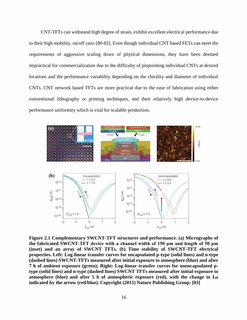
Figure 2.2 Fully printed CNT-TFTs and analysis of different CNT-metal contact
interfaces[61]. (a) Schematic diagram of a printed, back-gated CNT-TFT with indication of
key dimensions using AJP techniques. (b) Schematic structures of the three different contact
configurations studied in this work: top, bottom, and double contacts, as well as comparison
of contact resistance for printed CNT-TFTs having different printed electrode materials (Ag,
Au, and M-CNTs) and contact geometries (top, bottom, and double). Copyright (2016) ACS
Publications.
Cao et al. analyzed different contact resistance in fully printed CNT-TFTs fabricated using
AJP techniques[61]. Three different contact geometries including top, bottom and double (a
sandwich-like structure combining contacts below (bottom) and above (top) the printed CNTs) are
illustrated in Figure 2.2. They demonstrated that double contacts offered a significant decrease in
contact resistance in CNT-TFTs for different electrode materials compared to top and bottom

22
contact geometries. Besides, using M-CNTs as contacts were proved to be one of the best options
for enhancing performance of the CNT-TFTs. The bottom contacts were able to boost the on
current by up to 50% compared to the top contacts. Similar work can be found in [110-115].
2.1.7 Performance Analysis of CNT-TFTs
Kim et al. fabricated high-performance transparent electrodes and FETs using SWCNT and
graphene hybrid thin film. The high-performance was achieved by controlling the density and
alignment of pre-coated SWCNTs at the optimized spin-coating speed. Compared to the previous
work, they improved the on/off ratio and on-state current with respect to pristine graphene, and
the hybrid film possessed a sheet resistance of 300 Ω/sq with 96.4% transparency.[116]
It is well known that n-type SWCNT transistors are much difficult to achieve because of
various issues related with n-type doping strategies, e.g., limited carrier concentration modulation,
environmental instability, undesirable Vth control, and/or poor morphology. Geier et al. reported
controlled n-type doping of SWCNT thin-film transistors with a solution-processed
pentamethylrhodocene dimer. Consistent n-type behavior was observed for the charge transport
properties of organorhodium-treated SWCNT thin films when characterized in both Hall effect
and thin-film transistor geometries. Their work can facilitate ongoing efforts to realize high-
density SWCNT based ICs.[117]
Ha et al. also studied air-stable n-doping of CNT-TFTs by utilizing SiNx thin films deposited
by plasma enhanced CVD. Different from commonly used methods in the past, the fixed positive
charges within SiNx act to n-dope the underlying nanotubes via field-effect, which presented a
reliable and easy process route toward obtaining high performance SWCNT n-type transistors.
Moreover, excellent device-to-device uniformity was also achieved for these n-type CNT-TFTs
23
with comparable electrical characteristics to their p-type counterparts. Their work is significant
toward realization of CMOS circuitry based on CNT-TFTs for large-area electronic
applications.[118]
Jeon et al. demonstrated high-performance SWCNT-TFTs by reducing the charge transfer
using an interacting fluoropolymer encapsulation with thermal annealing in vacuum. As results,
the on-current increased, the off-current reduced, the Vth shifted toward 0 V, and the subthreshold
swing improved. Those improvement are the crucial to realize high-performance micorelectronics
with low power consumption. They also investigated the instability characteristics of the SWCNT-
TFTs during the prolonged electrical bias-stress. The drop in drain current of the SWCNT-TFTs
was partially recovered with a second phenomenon that increases the drain current after a certain
time.[119]
Choi et al. reported TFTs with highly uniform SWCNT nanomesh network fabricated from
a pre-separated semiconducting nanotube solution. The nanomesh structure can be formed using
oxygen plasma with etched nanoscale holes over the entire CNT network channel. These devices
could achieve on/off ratio as high as 106 (or even higher), which was superior for application in
large-scale ICs. The on/off ratio increased with the decreasing distance between the nanoscale
holes in the nanomesh network while maintaining a high degree of uniformity, which attributed to
the effective elimination of metallic paths across the source/drain electrodes by forming the
nanomesh structure in the high-density SWCNT network channel.[120]
Thermal issues also can be critical to the realization of high performance of CNT based
devices[121, 122]. Lee et al. investigated the coupling between thermal and electrical effects of
SWCNT based devices using an atomic force microscope (AFM) cantilever that is capable of

24
applying local electric and temperature fields in both contact and amplitude modulation modes.
They found tip-CNT thermal resistance was estimated at 1.6×10⁷ K/W and decreased with
increasing temperature. The ability to measure thermal coupling to a single-molecule electronic
device could offer new insights into CNT based devices in micro and nano scale.[123]
2.2 Fabrication of CNT-TFTs
2.2.1 Photolithography
PL is one of the most important methods for ICs fabrication [124]. Compared to printing
techniques, CNT-TFTs fabricated from PL exhibit much better electrical performance such as
higher carrier mobility and lower operation voltage [21]. More importantly, it can well control the
exact size/shape of the designed features and ensure resolution <100nm, especially when using
electron-beam lithography the resolution can reach sub-10nm level. However, multiple
photolithographic processes are indispensable for different patterns or layers. Typically, more than
10 masks might be needed for certain ICs fabrication, and each requires an extremely clean
condition in order to avoid possible contamination and environmental hazards. In general,
conventional lithographic patterning and vacuum processes will result in high-cost and low-
throughput processing.
2.2.2 Inkjet Printing
IJP has been widely used as a free-form fabrication technology for building three
dimensional layer-by-layer patterns and an effective way to fabricate flexible microelectronic
devices [34, 125, 126]. Typically, inkjet printers are able to handle inks with viscosities less than
20 centipoise (cP) and achieve resolution as small as 20 µm. Compared to conventional

25
lithography, low-cost is one of its greatest advantages. Another tremendous advantage lies in its
design versatility and operational flexibility. Due to the drop-by-drop printing method, inkjet
printers are capable of printing any desired features on demand within its resolution limits, which
makes it an efficient solution for cost-effective and scalable production.
Figure 2.3 Printed CNT based transistors using different printing techniques. (a)
Micrograph of the inkjet printed NAND gate based on SWCNT-TFTs[127]. (b) Fully-
printed, flexible, and hysteresis-free CNT-TFTs using aerosol jet printing (AJP)[68].
Copyright (2017) Nature Publishing Group and (2017) Wiley-VCH Verlag.
Vaillancourt et al. reported all inkjet printed CNT-TFTs on flexible substrates. The entire
fabrication was free from PL [128]. In Figure 2.3(a), Kim et al. fabricated ambipolar CNT-TFTs
mainly by IJP, which can be used for complementary circuits for sensor applications in ambient
conditions [127]. In this work, ALD was applied for dielectric layer because dielectric printing is
quite challenging for inkjet printers when considering its thickness and uniformity. Grubb et al.
reported 100% inkjet printed transistors with channel length as short as 0.3-2µm, which was
accomplished by using silver inks with different chemical properties to prevent mixing [129]. Cao

26
et al. also obtained fully printed CNT-TFTs using IJP with dramatically enhanced on-state current
density to ∼4.5 μA/μm[130]. Surprisingly, their CNT-TFTs actually achieved a sub-micron
channel length with top-contact self-aligned printing and employing high capacitance ion gel as
the gate dielectric, which may pave the way for future high-definition printed displays, sensing
systems, and low-power consumer electronics[131-133]. Other important publications focusing on
IJP based fabrication can be seen from [134-140].
2.2.3 Aerosol Jet Printing
AJP begins with atomization of liquid ink, producing droplets ranging 1-5μm in diameter.
The atomized droplets are delivered to the print head with an annular flow of clean nitrogen (N2)
gas wrapped around in order to focus the droplets into a tightly collimated beam of material. Then
this printable stream exits a converging nozzle at a controllable flow rate and then can be deposited
onto the target surface with relatively high velocity[58, 59, 141-146]. AJP has been proven to be
capable of printing microelectronic devices and relevant circuits with relatively high precision,
which is noncontact injection with high repeatability and scalability. AJP is also low in cost
compared to PL process. Like IJP, it has the ability to print fine and easily controllable patterns or
layers but with higher resolution (<10µm). The most significant advantage of AJP is that it can
deal with a much wider range of inks with viscosities >1000 cP.
AJP has also been successfully used for CNT-FET fabrication. Rother et al. investigated the
suitability of AJP of polymer-sorted (6,5) SWCNTs for top-gate FETs[147]. No impact was found
on the quality of the SWCNTs in terms of defects and length after sonication during the printing
process. Reproducible device performance was guaranteed over extended printing periods and for
different ink batches with constant printing parameters. Ha et al. fabricated sub-3V digital circuits

27
on plastic by AJP of CNT network, ion gel dielectric, and conducting polymer gate electrode
sequentially from liquid inks [65]. Cardenas et al. reported in-place printing of CNT-FETs with
Ag-CNT contacts at low temperature using AJP[148]. No external baking, coating, or other
treatments were involved during fabrication after the substrate was loaded, which ensured entirely
in-place, from first step to last, without removal of the substrate from the printer. In Cao et al.’s
work, they explored the printing of hydrophobic dielectric layer (xdi-dcs) based on AJP for their
hysteresis-free CNT-TFTs, depicted in Figure 2.3(b) [68]. Another work from Cao et al. focused
on improving the contact interfaces in AJP printed CNT-TFTs, where contact resistance dominates
the performance and degree of variability in these TFTs [61]. Similar work can be found in [58,
149-152]. However, the thick printed dielectric layer highly limits the performance of printed
CNT-TFTs because high gate bias is required to switch on/off the devices. More work needs to be
done considering the quality of printed dielectric layer in order to improve the overall performance.
2.2.4 Screen Printing
Screen printing, also known as serigraphy or screen process, is a printing technique
whereby a thick paste ink is forced through a stencil attached to a finely-woven mesh screen,
transferring ink to the desired substrate except in areas made impermeable to the ink by a blocking
stencil[153]. Similar as IJP and AJP techniques, it is also a relatively simple and inexpensive way
to make detailed prints on a diverse set of substrates including paper, polyimide, bumper stickers,
posters, cloth, etc.[154, 155]
Cao et al. utilized screen printing as simple, scalable, and cost-effective approach for both
rigid and flexible SWCNT-TFTs[156]. The fully printed transistors exhibited decent performance,
with mobility up to 7.67 cm2 V-1 s-1, on/off ratio of 104 ∼ 105, minimal hysteresis, and low
28
operation voltage (<10 V). They also demonstrated outstanding mechanical flexibility of the CNT-
TFTs bent with radius of curvature down to 3 mm. Another work from Cao et al. focused on CNT-
TFT based large-area and flexible active-matrix electrochromic displays (AMECD), which were
also fabricated by screen printing[157]. This fully printed backplane showed high electrical
performance with mobility of 3.92 ±1.08 cm2 V-1 s-1, on/off ratio ∼104, and good uniformity. To
obtain an entirely screen-printed AMECD, they monolithically integrated the printed backplane
with an array of printed electrochromic pixels, which resulted in devices with good switching
characteristics, facile manufacturing, and long-term stability. Bandodkar et al. reported fully
printed CNT-based electrochemical sensors and biofuel cells using screen printing technique for
large-scale fabrication[158]. These devices were highly stretchable and could withstand strains as
high as 500% with very limited effect on their structural integrity and electrochemical
performance. This work lays the foundation for scalable, low-cost, and highly stretchable CNT
based devices for wide range of applications in healthcare, consumer electronics etc.
2.2.5 Roll-to-roll Gravure Printing
During roll-to-roll gravure printing, the ink or paste is rolled over the engraved cylinder first
and then wiped to remove excess ink from the non-image areas of the gravure roll using a doctor
blade. The ink is compressed, stretched, sheared, fractured, and then transferred to the substrate.
During the printing process, the effectiveness of excess ink removal from the non-image areas
highly depends on two major factors: (1) the viscosity of the ink under a given roll speed, and (2)
the doctor blade angle. [159]
Koo et al. demonstrated roll-to-roll gravure printing as a suitable manufacturing technique
for flexible CNT-TFT based electronic circuits[160, 161]. Fully printed SWCNT-TFTs with

29
different channel sizes were fabricated on 150-m-long rolls of 0.25-m-wide poly(ethylene
terephthalate) (PET) using silver nanoparticles, BaTiO3 nanoparticles, and SWCNTs ink. A Monte
Carlo simulation for a 1-bit adder circuit was conducted to demonstrate the feasibility of roll-to-
roll gravure printing for functional circuits with reasonable complexity. Noh et al. fabricated fully
roll-to-roll gravure printed D flip-flop on flexible plastic foils using p-channel SWCNT-TFTs for
the first time, which shows a clock-to-output delay of 23 ms for 20-Hz clock signal[162].
Combined printing methods are also of large interest. Fully printed CNT-TFTs were fabricated by
Homenick et al. [126]. This printing process combined roll-to-roll gravure for gate/dielectric and
IJP for CNTs/source/drain, which yielded CNT-TFTs with good operational stability.
2.3 Applications
2.3.1 Flexible Electronics
Due to the excellent properties of CNTs such as high conductivity, intrinsic carrier mobility,
mechanical flexibility, stability and reliability, they have been widely used as material for flexible
electronics. In most of the cases, CNTs are the semiconducting material (either single CNT or
CNT thin film) in the channel of FETs, which are the elemental building blocks for flexible
electronics. They also can be applied as transparent electrodes, sensor materials, etc. in other
applications. Two major processing methods have been extensively utilized for CNT film
fabrication, which are CVD based and solution/ink based method. One of the biggest advantages
of CVD based CNTs is that they can be highly aligned for better performance. However,
solution/ink based CNTs is more convenient for large-scale fabrication and especially compatible
for printed flexible electronics, which is beyond the capability of CVD based method. Besides, the

30
low cost of solution based CNT film deposition make them suitable for the development of future
flexible and wearable devices.
Figure 2.4 (a) Devices on PEN substrate. (b) Optical micrograph and circuit diagram of a
21-stage ring oscillator. (c) Optical micrograph and input–output characteristics master–
slave delay flip-flop[164]. Copyright (2011) Nature Publishing Group.
Wang et al. fabricated extremely bendable devices using SWCNT-TFTs on a flexible
substrate, which offers high performance, low cost, ambient stability, and significantly outruns the
organic semiconductor materials [21]. Such devices are proven to be practical for digital, analog
and radio frequency (RF) applications. Cao et al. reported medium-scale CNT thin-film devices
on plastic substrates using sub-monolayer SWCNT networks to yield small to medium-scale
integrated digital circuits, composed of up to nearly 100 transistors [163]. The sub-monolayer films
are superior materials for flexible ICs, with potential applications in consumer and other areas of
electronics. Sun et al. investigated high performance flexible devices using CNT-TFTs exhibited

31
in Figure 2.4 [164]. They not only demonstrated flexible ICs, including a 21-stage ring oscillator
and master–slave delay flip-flops that are capable of sequential logic, but also pointed out the
lithographic techniques can be replaced with printing techniques in order to develop large-scale,
low-cost and flexible electronics. Other similar applications include flexible circuits[163-166],
flexible displays[167-169], flexible sensors[170-174], flexible solar cells[175-177], artificial
skin[56, 178], and conformable RFID tags[14, 124], etc.
Table 2.1 Summary of selected sensing performance (N/S = Not-stated) [25]
CNT type Sensor
configuration Targeted analytes Detection limit
Response time (s)
Reversibility
Single SWCNT
ChemFET NO2, NH3 2 ppm (NO2) 0.1%
(NH3) <600 Irreversible
SWCNTs ChemFET Alcoholic vapors N/S 5-150 Reversible
SWCNTs Chemiresistor O2 N/S N/S Reversible
SWCNTs ChemFET DMMP <1 ppb 1000 Reversible
MWCNTs Chemiresistor NO2 10 ppb N/S Reversible
(165℃)
SWCNTs Chemiresistor NO2, Nitrotoluene 44 ppb (NO2), 262 ppb (Nitrotoluene)
600 Reversible
(UV)
MWCNTs Chemiresistor NH3 10 ppm ~100 Reversible
SWCNTs Chemiresistor SOCl2, DMMP 100 ppm 10 Irreversible
SWCNTs Chemiresistor O3 6 ppb <600 Reversible
MWCNTs Chemiresistor NO2 5-10 ppb ~600
(165℃) Reversible
(165℃)
SWCNTs Chemiresistor methanol, acetone N/S ~100 N/S
SWCNTs Chemiresistor H2O N/S 10-100 Reversible
Carboxylated SWCNT
Chemiresistor CO 1 ppm ~100 Reversible
2.3.2 Sensors and Actuators
The special structure of being composed entirely of surface atoms makes CNTs an ideal
material to detect electrical signals resulting from interaction with different gas molecules.

32
Generally, chemical field-effect transistors (ChemFET) and chemiresistors are two typical gas
sensors. Table 2.1 summarizes the sensing performance of some pristine CNT gas sensors from
previous work. Snow et al. demonstrated that the capacitance of SWCNTs is highly sensitive for
both polar and non-polar gas molecules at room temperature [179]. MWCNTs were used in gas
sensors by Ong et al. for the detection of CO2, O2, and NH3 [180]. They developed a wireless,
passive MWCNT-SiO2 sensors based on changes of relative permittivity and conductivity of the
material. Functionalization of CNTs can not only increase the sensitivity, but also well address the
potential drawbacks: lack of selectivity to different gaseous analytes. Kuzmych et al.
functionalized the SWCNT networks with poly (ethylene imine) (PEI) non-covalently to detect
NO in exhaled breadth, which reached detection limit ~5ppb in air [181]. Guerin et al. fabricated
different electrode metals on top of horizontal CNT arrays [182]. These structures can take
advantage of the specific interaction for each metal/CNTs/gas case to discriminate different gases
at room temperature. Abdelhalim et al. utilized different metals to alter the response of each
sensing element towards different gases, which can discriminate four gases: NH3, CO, CO2, and
ethanol [183].
CNTs can be also used as material for other different types of sensors. Lipomi et al.
fabricated skin-like pressure and strain sensors based on transparent elastic CNT films[173]. Even
though the sensors showed less sensitivity compared to previously reported work, but they were
the first transparent and stretchable devices which could detect both pressure and strain. Besides,
those devices were monolithically integrated, extremely mechanically compliant, physically
robust and easily fabricated. Liu et al. applied synergistic CNTs and graphene bifillers in strain
sensors[184]. The dispersion of CNTs and formation of effective conductive paths were
strengthened when graphene acted as a ‘spacer’ to separate the entangled CNTs from each other.
33
The sensors showed good reversibility and reproductivity under cyclic extension. As biosensors,
CNTs can be modified with suitable groups capable of recognizing biomolecules (e.g., proteins
such as enzymes and antibodies) and also can be modified with a biological sensing element (e.g.,
nucleic acids and peptides)[33]. Shah et al. reported electrochemical sensors based on SWCNT-
modified glassy carbon electrodes for the sensitive detection of valacyclovir[185]. The
electrochemical oxidation of valacyclovir was investigated using cyclic voltammetry and
differential pulse voltammetry. Results revealed the proposed sensors had a lower detection limit
compared to the previously reported instrumental analysis.
Figure 2.5 (a) Characterization of the self-aligned T-shape gate transistors based on aligned
polyfluorene-sorted CNTs. (b) Comparison of the RF performance between different CNT
based transistors. The extrinsic frequency response (left). The intrinsic frequency response
with the device de-embedding structure (middle). The intrinsic frequency response with the
intrinsic de-embedding structure (right) [186]. Copyright (2016) ACS Publications.

34
2.3.3 Radio Frequency Applications
Cao et al. reported RF transistors using well-aligned S-CNTs with current-gain cutoff
frequency and maximum oscillation frequency simultaneously greater than 70GHz[186]. As
shown in Figure 2.5, these transistors showed outstanding direct current performance with on
current density of 350 μA/μm, transconductance of 310 μS/μm, and superior current saturation
with normalized output resistance greater than 100 kΩ·μm, and also exhibited good linearity
performance with 1 dB gain compression point of 14 dBm and input third-order intercept point of
22 dBm. Their contribution in CNT based RF electronics will broaden the applications for signal
amplification, wireless communication, and wearable/flexible electronics. Wang et al. studied RF
and linearity performance of CNT-FETs using high-density, uniform S-CNT networks[187]. The
channel length of the RF transistors was fabricated as small as 500nm, exhibiting a cutoff
frequency of 5 GHz and with maximum oscillation frequency of 1.5 GHz, with linearity metrics
up to 1 GHz. Those RF transistors are promising building blocks for highly linear RF electronics
and circuit applications. Vincent et al. performed a systematic study of the use of resonating
nanotubes in a field emission configuration to demodulate RF signals and explored the use of
CNTs undergoing field emission as nanoantennae and the different geometries that could be used
for optimization and implementation[188].
2.3.4 Batteries and Energy Devices
Yu et al. described a hierarchically structured carbon microfibre made of an interconnected
network of aligned SWCNT with interposed nitrogen-doped reduced graphene oxide sheets[189].
They fabricated capacitor electrodes using these fibres, which showed a specific volumetric
capacity of 305 F cm-3 in H2SO4 and 300 F cm-3 in polyvinyl alcohol (PVA)/H3PO4. They also

35
fabricated a full micro-supercapacitor with PVA/H3PO4 gel electrolyte, which has a volumetric
energy density of ∼6.3 m Wh cm-3 while maintaining a power density more than two orders of
magnitude higher than that of batteries. Their device could bridge the energy density gap between
microbatteries and micro-supercapacitors for miniaturized portable electronics. Lee et al. used
layer-by-layer techniques to assemble an electrode with MWCNTs, which was an alternative
approach based on the redox reactions of functional groups on the surfaces of CNTs[190]. A
gravimetric energy ∼5 times higher than conventional electrochemical capacitors and power
delivery ∼10 times higher than conventional lithium-ion batteries were achieved by using the CNT
electrode as the positive electrode and lithium titanium oxide as a negative electrode. Kim et al.
electrodeposited MnOx nanoparticles onto CNT sheets for high-performance energy storage
devices, which can be used as electrodes for lithium batteries and supercapacitors[191].
2.3.5 Other Applications
CNT-TFTs are promising for optically transparent and flexible display electronics. Zhang et
al. reported separated CNT macro-electronics for a monolithically integrated active matrix organic
light-emitting diode (AMOLED) displays on glass substrates [192]. It exhibits huge advantages
for the next generation visual technologies due to its high light efficiency, flexibility, lightweight,
and low-temperature processing. High performance ICs is another important application of CNT-
TFTs. Chen et al. built medium scale ICs using CNT-TFTs [35]. Logical/arithmetical gates,
shifters, and d-latch circuits were designed and demonstrated with rail-to-rail output with superior
performance. Besides, as the maturity of printing techniques, many wearable devices have been
put into use with outstanding flexibility and stability, such as artificial electronic skin,
chemical/biological sensors, solar cells, and stretchable electrode for actuators [20, 80, 124].

36
However, significant challenges still exist in many aspects, e.g., (a) device-to-device
performance variation is becoming a critical problem for reliability and stability consideration as
well as circuit design; (b) the lack of selectivity of CNT based gas sensors can severely limit their
applications in gas detection and gas identification; (c) for printed TFTs, the uniformity of printed
CNT network and roughness/thickness of dielectric layer will be a major obstacle to achieve higher
device performance; and (d) the application of flexible sensors is the trend in the future. It is critical
to make best of the tradeoff between high sensitivity and low cost, which needs further studies,
etc. Undoubtedly, all of these need to be analyzed and understood thoroughly.
2.4 Contributions of Current Work
The important findings and the major contributions of the current work are listed below
(1) A systematic study of variability in I-V characteristics has been performed in a statistical
framework through a combination of experimental and theoretical analysis of the major
sources which cause performance variation. For the experimental analysis, array of
CNT-TFTs are fabricated using high-k dielectric HfO2 as gate oxide layer to achieve
high performance (PL fabrication). For the theoretical part, we apply the current scaling
relationship developed by Pimparkar et al.[193] and analyze each variable used in the
relationship, which can be a major source of variability. The sources of variation
including % of M-CNTs, Vth, CNT mean length and CNT network density have been
studied separately. The analysis shows that the presence of m-CNT is a major source
contributing to the performance variation for short channel TFTs, but its effect reduces
for large channel length transistors. Vth is found to be the major source of variation for
long channel TFTs. A better consistency in performance can be guaranteed for TFTs

37
with larger channel area, which ensures a smaller variation in CNT network density and
CNT mean length. These results provide key insights into the variability estimation of I-
V characteristics of CNT based devices which is vital for reliability studies of CNT-
TFTs based circuits for different electronic applications.
(2) CNT-TFTs have been fabricated using randomly distributed CNT network (PL
fabrication) and they are investigated for NH3 and NO2 detection at low ppm
concentrations. Sensor response from NH3 and NO2 spray at 2ppm-40ppm has been
measured in air at room temperature. A sensing mechanism is proposed based on the
interaction between gas molecules and different types of dwelling spots inside the
channel area of a TFT. We present double exponential-convolution model to decipher
sensor response as well as to explore its application in gas identification. In this context,
the consistency in time constants is recognized, which is independent of gas
concentration. More importantly, the time constants vary with respect to different gas
types and TFTs. The uniqueness of time constants can work as identity verification for
different sensing gases, which demonstrates that the sensor response is a distinctive
behavior determined by the unique channel structure of each TFT. It provides a general
strategy for gas identification in ppm level and a practical path to realize the advantages
of CNT gas sensors in air quality detection as well as the industrial emission control.
(3) Fully printed CNT-TFTs have been fabricated (AJP fabrication) on Kapton and PET
substrates with high on/off ratio, high mobility, negligible hysteresis, and good
uniformity. More importantly, the fully printed CNT-TFTs can be operated using bias
voltages ~ ±5V, which is much smaller than the previously reported values because of
the improvement in both CNT network and dielectric layer. Multiple layer by layer CNT

38
network deposition is applied for density control and high uniformity, and xdi-dcs is
diluted and optimized with natural ≥99.5% butyl alcohol to reach thinner printing for
better gate dielectric quality. The performance was highly improved by optimization of
xdi-dcs layer for the first time, which is key for CNT-TFTs based flexible electronics to
achieve lower voltage operation and power dissipation. This paves the path for
applications of CNT-FETs in wearable and bendable devices such as flexible displays,
RFID antennae/tags, sensors, artificial skins, etc.
(4) CNT networked gas sensors are fabricated base on printing techniques (AJP and IJP
fabrication). The fully printed CNT sensors are applied for NH3 and NO2 detection in air
at low ppm concentration. Through comparison with CNT sensors fabricated by PL,
printed sensors show no degradation with respect to sensitivity and stability, but much
lower in cost. Especially for sensors using extremely low-cost IJP (with the printer price
only US $108), the corresponding sensor responses still show excellent performance.
The sensitivity was surprisingly high for some printed CNT sensors with drop-casted
CNT network. Moreover, the post drop-casted deposition (without any surface
functionalization) could help improve the sensitivity efficiently by rebuilding the CNT
network of low sensitivity sensors, which implies the extremely low-cost potential of
CNT gas sensors using IJP and drop-cast method. It provides key insights for the
application of extremely low-cost CNT gas sensors.

39
CHAPTER 3. PERFORMANCE VARIABILITY OF CNT-TFTS
In this Chapter, both experimental and theoretical methods were employed to analyze the
variability in I-V characteristics in a statistical framework. For the experimental analysis, array of
CNT-TFTs were fabricated using high-k dielectric HfO2 as gate dielectric to achieve high
performance. 40~50 devices of each series (same channel dimensions) were fabricated on a Si
wafer for the statistical study. For the theoretical part, the current scaling relationship [193] was
applied and each variable used in the relationship was analyzed, which can be a major source of
variability. To be specific, each variable was treated as a distribution function while keeping others
as constants. Variation sources such as % of M-CNTs, Vth, CNT mean length, and CNT network
density were studied statistically for different channel dimensions. For the first time, the variability
analysis of random CNT network based TFTs has been studied systematically. This analysis
presents an effective way of the variability estimation of CNT network based TFTs. Such analysis
of CNT-TFTs is crucial to explore the reliability and stability of CNT network based circuits and
to devise techniques which can help reduce variability in circuit performance for various electronic
applications.
3.1 Fabrication of CNT-TFTs
CNT-TFTs were fabricated at the Institute for Electronics and Nanotechnology (IEN)
cleanroom of Georgia Tech. The structure and fabrication process of a typical TFT are illustrated
in Figure 3.1. First, Ti/Au (5nm/50nm) layers as back gate were deposited on top of a Si wafer by
e-beam evaporation at deposit rate of 0.2Å/s and 1 Å/s respectively. The gate contacts were
patterned between the source/drain (S/D, deposited later) electrodes. Following this, ALD was
used to deposit TiO2 (1.5 nm/15 cycles) and HfO2 (75nm/600 cycles), covering the entire wafer

40
surface as a global gate-dielectric layer. Ti and TiO2 work as adhesion layers for the gate and gate
dielectric. Then, 15~30s oxygen plasma treatment was indispensable to make the surface
hydrophilic[81]. After this, CNT network was deposited by immersing the wafer into 0.005-
0.01g/L toluene-based CNT solution for 5-15 minutes (CNT source: >99% purity polymer-
wrapped CNT solution from NanoIntegris). The resulting density of the CNT network is a function
of both deposition time and concentration of the CNT solution. Ti/Au (5nm/50nm) layers as S/D
electrodes are patterned by PL and lift-off process. This step was followed by another PL and 30s
oxygen plasma treatment to form channel area by etching away unwanted part of the CNT network.
At last, vacuum annealing at 250°C for 2 hours was performed to get rid of the surface residue on
the wafer.
Figure 3.1 Fabrication of CNT-TFTs. (a) ~ (f) Fabrication process. (g) The sectional view of
the CNT-TFT. (h) CNT-TFTs fabricated in IEN cleanroom.

41
Figure 3.2 I-V characteristics. The overall I-V characteristics shows good performance of the
p-type CNT-TFTs with on/off ratio as high as 105 and mobility around 1-4 cm2 V-1 s-1.
3.2 I-V Characteristics of CNT-TFTs
After the fabrication, I-V characteristics of the CNT-TFTs had been measured using
Microtech Summit 11k probe station and Keithley 4200-SCS. The I-V of the CNT-TFTs is plotted
42
in Figure 3.2. The output characteristics (Id-Vds curves) of the CNT-TFTs is depicted in Figure
3.2(a) for different channel lengths with drain voltage (Vds) swept from 0 to -4V at Vgs=-1V, where
Id is the drain current and Vgs is the gate voltage. For the transfer characteristics (Id-Vgs curves),
Vgs was swept from -4~4V (forward sweeping) while keeping Vds = -1V. Semi-log plots are shown
in Figure 3.2(b) for each channel length. The on/off ratio increases from 103 to as high as 105 when
the channel length increases from 5µm to 60µm, which can be expected since the CNT networks
still contain M-CNTs even though it is purified for 99% semiconducting tubes. The on/off ratio is
a function of the channel length as the TFTs with smaller channel length have much higher
possibility to bridge the channel by M-CNTs. In Figure 3.2(c), the output characteristics at
different Vgs is plotted for a specific device. The overall I-V characteristics shows good
performance of the p-type CNT-TFTs with on/off ratio as high as 105 and mobility around 1-4 cm2
V-1 s-1
3.3 CNT Statistics
CNT network as well as individual CNTs play an important role for the fabricated CNT-
TFTs with respect to mobility, on/off ratio, Vth, etc. Before variability analysis, CNT length
distribution has been obtained using Auto CAD sampling and statistics based on the scanning
electron microscope (SEM) images of CNT network. Besides, CNT network density can be
estimated based on both Auto CAD sampling and image processing technique.

43
Figure 3.3 Statistics of CNT length distribution using Auto CAD software and a SEM image
of low-density CNT network. The white frame is selected randomly. The green splines denote
CNTs that will be recorded (the red ones will not be recorded). The scale bar is used as
calibration standard in order to calculate the real lengths of all the target CNTs.
3.3.1 Statistics of CNT Length Distribution
To obtain the CNT length distribution, we measure CNT length one by one from a much
lower density network using the same CNT solution. In this way, the overlapping between CNTs
can be avoided and each of them can be located individually. Then ‘spline’ of Auto CAD is used
to draw each CNT separately while setting the SEM image as background in Auto CAD workspace
as shown in Figure 3.3. After that, the length information of CNTs can be obtained by recording
the length of each ‘spline’. At last, calibration is performed by utilizing the scale bar in the SEM
image to calculate the real length information of the target CNTs.
In order to get accurate length distribution, different area is selected randomly (using
multiple white frames to repeat the described process) from different CNT network samples. And

44
for each target area (each white frame), only CNTs with >50% of its length inside the frame are
recorded, which can guarantee that all the CNTs will have the equal probability to be recorded no
matter what length it is. Considering hundreds of CNTs, the CNT mean length is measured to be
1.08µm (the suggested value from the vendor is ~1µm).
Figure 3.4 Estimation of CNT network density based on image processing by converting the
SEM image into a binary image. The inset of the sample image is used to estimate the average
diameter of all the CNTs in the target image.

45
3.3.2 Estimation of CNT Network Density
The CNT network density (ρ) is defined as the number of CNTs per unit area. To estimate
CNT network density in the channel of CNT-TFTs, an image processing technique is put forward
to convert the target SEM image of CNT network into the corresponding binary image by using
Matlab. Then the relationship between CNT network density and the white pixel of the binary
image can be established for the density estimation.
As shown in Figure 3.4, the target SEM image can be acquired through Zeiss Ultra60 FE-
SEM. To calculate the CNT network density of the target image, the corresponding binary image
can be generated to obtain the white pixel area (At_white), which denotes all the CNTs in the target
image. Then At_white can be expressed as
At_white = Dt_CNT × Lt_CNT (3.1)
where Dt_CNT is the average diameter of CNTs in the target binary image, and Lt_CNT is the total
length of all the CNTs in the target binary image. It is worth noting that the real diameter of
SWCNT is as small as 1-3nm, which cannot be used as Dt_CNT in equation (3.1). Dt_CNT will be
much larger because of the optical effect during SEM imaging. To estimate the value of Dt_CNT , a
sample area is selected and similar expression can be obtain for this sample binary image
As_white = Ds_CNT × Ls_CNT (3.2)
where Ds_CNT is the average diameter of CNTs in the sample binary image, and Ls_CNT is the total
length of all the CNTs in the sample binary image. To obtain the value of Ls_CNT, Auto CAD
sampling and statistics strategy has been used again as described in Figure 3.3. At_white and As_white
can be obtained from the corresponding binary images. Then assume

46
Dt_CNT = Ds_CNT (3.3)
Based on equation 3.1 – 3.3, Lt_CNT can be calculated as
Lt_CNT = Ls_CNT × At_white / As_white (3.4)
At last, the CNT network density (ρ) can be calculated as
ρ = Lt_CNT / At / Ls (3.5)
where At is the total area of the target image, and Ls is the CNT mean length (1.08μm) which has
been obtained in section 3.3.1. As a result, the CNT network density is calculated as 11.718 / µm2
in the target image. Clearly, the assumption of equation 3.3 is the key during the calculation, which
depends on the selection of the sample area. As a matter of fact, the value of Ds_CNT is very stable
in most of situation when the SEM image is taken properly. If Ds_CNT depends much on the
selection of sample area, multiple sample area should be selected in order to satisfy the assumption
of equation 3.3. This method is proved to be very reliable for the estimation of CNT network
density.
3.4 Source of Variation and Variability Analysis
This study focuses on the variability analysis of I-V characteristics of CNT-TFTs. The
performance variation results from multiple sources, described below:
On the level of individual CNTs
One of the major sources of variability lies in the large difference of electronic properties
between M-CNTs and semiconducting S-CNTs. Generally, as-grown CNT networks contains 33%
M-CNTs, which largely limit the function of gate to achieve high on/off ratio[1]. In Figure 3.2, the

47
on/off ratio varies from 103 to 105 for different channel lengths even though 99% purified CNT
solution (i.e., 99% S-CNT and 1% M-CNT) were used. The length distribution of CNT is another
source of variability. In our CNT networks, the average length of CNT is ~1µm. However, some
CNTs can be > 5µm while some other CNTs can be as short as 0.1µm. The performance variations
for the short channel TFTs will be much higher since longer CNTs can directly bridge the source
and drain with much higher probabilities[193]. Besides, difference in diameter, morphology,
doping of individual CNTs may also contribute to the variability in I-V characteristics[194, 195].
On the level of the CNT networks
On the one hand, CNT network density has a significant effect on the drain current, which
has been studied intensively in the recent years. The significant performance variations can result
from the density variation since it cannot be controlled perfectly in practice. No matter how a CNT
network is fabricated in a TFT, density will vary from region to region. On the other hand, CNT
network structure can be another reason for variability. For TFTs with the same channel length
and the same network density, performance variations still exist because the randomly distributed
CNTs make each network structure different from each other. Although each TFT has different
network structure, variability can be deciphered in a statistical framework by studying TFTs with
a range of channel dimensions and network densities.
On the level of the device
The variation in Vth can lead to significant variation in I-V characteristics and device
performance. Vth can be obtained for each TFT and its effect on the variability can be
quantified[72, 196, 197]. Many imperfections may exist during the fabrication process which can
be significant sources of variation, e.g., variations in oxide layer thickness, contact patterns,

48
contamination region by region etc.
In general, the sources described above at different levels can contribute to the final
performance variation. It is impossible and needless to analyze each cause one by one. But
capturing the effect of most important sources is rather reasonable and feasible. Contact resistance
(Rc) between CNTs and electrodes has been ignored because Rc is small compared to the total
resistance (RSD) of the random CNT networks considered. Using a transfer length method (TLM),
Rc is estimated to be ~6.8kΩ which is less than 1% of the average total resistance (RSD) of the
smallest channel length considered (~5µm). The reason for high RSD is rooted in the large number
of CNT-CNT junctions inside a randomly generated CNT network, which dominates the total
resistance. In the following discussion, variation in I-V characteristics of TFTs were analyzed and
compared by both experimental and theoretical means. Experimental data corresponds to the I-V
characteristics measured for the TFTs fabricated at Georgia Tech’s IEN. Theoretical data were
obtained using the empirical formula developed by Pimparkar et al. [193].
CNT-TFTs with three different channel length series (L=5µm, 10µm, and 50µm) were
considered and referred as 5µm series, 10µm series, and 50µm series, respectively. For each series,
we fabricated 45 CNT-TFTs and analyzed the variability of I-V. The transfer and output
characteristics was measured for CNT-TFTs with 5µm, 10µm, and 50µm series. For output
characteristics, Vds was swept from 0 to -2V at Vgs= -1V. From Figure 3.5(a)~(d), it is obvious that
TFTs with longer channel lengths have smaller current magnitude. It can be also noted that the
longer channel TFTs have a smaller range of variation in the saturated current, referred as Id(sat) .
From the experimental data, the range of variation in Id(sat) of L=5µm, 10µm, and 50µm series are
(-1×10⁻⁶, -0.6×10⁻⁷), (-4×10⁻⁷, -0.5×10⁻⁷), and (-2.1×10⁻⁷, -0.4×10⁻⁷). Their mean values are -
2.8×10⁻⁷, -1.7×10⁻⁷, and -1.3×10⁻⁷respectively. Here the unit of current is A by default unless stated

49
otherwise. For the TFTs whose current does not saturate in the range of sweep voltage considered,
the Id(sat) corresponds to the maximum magnitude of the measured current. The average Id-Vds
curves for each series are illustrated in Figure 3.5(b)~(d) by green curves. The Id(sat) distribution
can be found in Figure 3.6. The standard deviations for 5µm, 10µm, and 50µm series are 1.7×10-
7, 7.7×10⁻⁸, and 4.1×10⁻⁸, respectively. And the corresponding standard deviation normalized by
mean are 0.61, 0.45, and 0.32 respectively. From the experimental data, it can be deciphered that
the longer channel length TFTs are more stable and have less variations in performance.
Figure 3.5 Measured output characteristics of fabricated CNT-TFTs. All devices are shown
together in (a), and shown separately for 5µm series (b), 10µm series (c), and 50µm series (d).
Green curves in (b)~(d) denote average output characteristics.
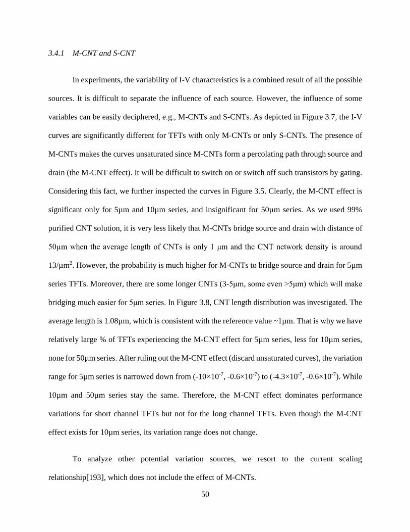
50
3.4.1 M-CNT and S-CNT
In experiments, the variability of I-V characteristics is a combined result of all the possible
sources. It is difficult to separate the influence of each source. However, the influence of some
variables can be easily deciphered, e.g., M-CNTs and S-CNTs. As depicted in Figure 3.7, the I-V
curves are significantly different for TFTs with only M-CNTs or only S-CNTs. The presence of
M-CNTs makes the curves unsaturated since M-CNTs form a percolating path through source and
drain (the M-CNT effect). It will be difficult to switch on or switch off such transistors by gating.
Considering this fact, we further inspected the curves in Figure 3.5. Clearly, the M-CNT effect is
significant only for 5µm and 10µm series, and insignificant for 50µm series. As we used 99%
purified CNT solution, it is very less likely that M-CNTs bridge source and drain with distance of
50µm when the average length of CNTs is only 1 μm and the CNT network density is around
13/µm2. However, the probability is much higher for M-CNTs to bridge source and drain for 5µm
series TFTs. Moreover, there are some longer CNTs (3-5μm, some even >5μm) which will make
bridging much easier for 5μm series. In Figure 3.8, CNT length distribution was investigated. The
average length is 1.08µm, which is consistent with the reference value ~1µm. That is why we have
relatively large % of TFTs experiencing the M-CNT effect for 5µm series, less for 10µm series,
none for 50µm series. After ruling out the M-CNT effect (discard unsaturated curves), the variation
range for 5µm series is narrowed down from (-10×10-7, -0.6×10⁻⁷) to (-4.3×10⁻⁷, -0.6×10⁻⁷). While
10µm and 50µm series stay the same. Therefore, the M-CNT effect dominates performance
variations for short channel TFTs but not for the long channel TFTs. Even though the M-CNT
effect exists for 10µm series, its variation range does not change.
To analyze other potential variation sources, we resort to the current scaling
relationship[193], which does not include the effect of M-CNTs.

51
2( , ) ( , )Sd S gs ds
S
LAI L f V V
L L = (3.6)
Here, Id is the drain current and the proportionally constant A depends on the oxide capacitance,
CNT diameter and CNT-CNT interaction parameter[72]. Ls is CNT mean length. ξ and f are
functions of the geometrical parameters (Ls, L and ρ) and bias conditions (Vgs and Vds), where L
is channel length, ρ is CNT network density, Vgs is gate bias voltage, and Vds is drain bias voltage.
ξ can be expressed as
2( )
2( , )
Sm L
S SS
L LL
L L
=
(3.7)
Here, m is a universal exponent of CNT percolating system, which is a function of ρ and Ls. This
relation is derived and analyzed in [193]. The bias-dependent scaling function
21( , ) [( ) ]
2gs ds gs th ds dsf V V V V V V= − − (3.8)
is independent of the geometrical parameters, where Vth is threshold voltage. Plugging (3.7) and
(3.8) into (3.6), the current scaling relationship can be expressed as
21[( ) ]
2
m
Sd gs th ds ds
S
LAI V V V V
L L
= − −
(3.9)
Theoretically, all the listing variables will have effects on the variation of Id. By
considering each variable as a statistical distribution such as normal or lognormal distribution, the
corresponding distribution for Id can be obtained.
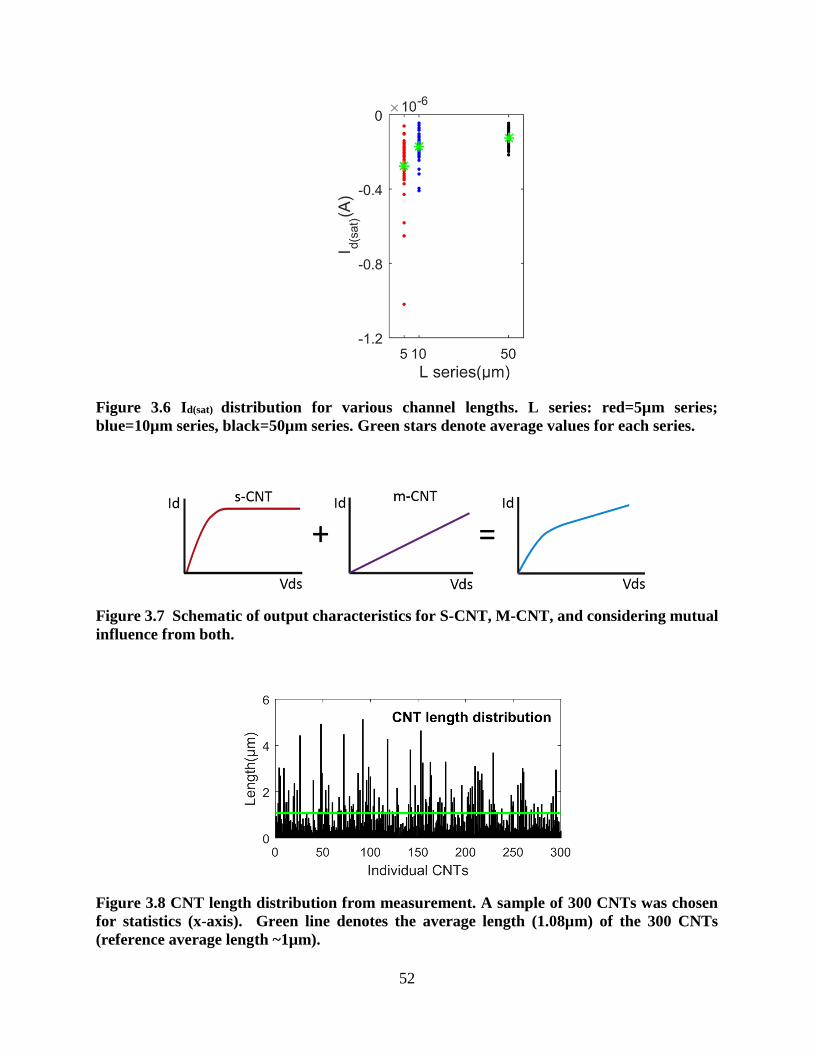
52
Figure 3.6 Id(sat) distribution for various channel lengths. L series: red=5µm series;
blue=10µm series, black=50µm series. Green stars denote average values for each series.
Figure 3.7 Schematic of output characteristics for S-CNT, M-CNT, and considering mutual
influence from both.
Figure 3.8 CNT length distribution from measurement. A sample of 300 CNTs was chosen
for statistics (x-axis). Green line denotes the average length (1.08µm) of the 300 CNTs
(reference average length ~1µm).

53
3.4.2 Threshold Voltage
The Vth distribution was considered as a source of variability in the I-V characteristics.
Ortiz-Conde et al. studied multiple methods to obtain Vth from the transfer characteristics [197],
e.g., by linear extrapolation of the Id-Vgs curve at its maximum first derivative point and finding
the intercept of the gate bias axis. Using this method, Vth was extracted from the measured Id-Vgs
curves where Vgs was swept from -4~4V at Vds =-1V. Id-Vgs curves are shown in Figure 3.9(a)~(b)
under both linear and semi-log axes for Vgs. The results for Vth are presented in Figure 3.9(c)~(e)
for 5µm, 10µm, and 50µm series separately. The corresponding distribution of Vth can be found
in Figure 3.9(f). Average Vth equals to -0.39V, -0.25V, and -0.13V, and standard deviation of Vth
equals to 0.17, 0.25, and 0.23 for 5µm, 10µm, and 50µm series, respectively. Even though Vth
shows increasing trend with increasing channel length, such trend should not be generalized for
other TFTs. We do not have experimental data and evidences to accurately explain the physics
behind this observation. Vth can be affected by many factors such as random dopant fluctuation,
different types of oxide charges, body effect, etc. and the observed trend can be a combined
influence of these parameters. Vth can be represented as a normal distribution, which is shown in
inset of Figure 3.9(f).
Using the Vth distribution estimated from the experimental data, we obtained series of
output characteristics from equation 3.9 by setting the rest of variables constants (Ls=1.08µm,
Vgs=-1V, m=1.05, L=5µm, 10µm, and 50µm for each series). Ls=1.08µm is CNT mean length,
and m=1.05 is determined by average CNT network density, which is ρ=13/µm2. The value of A
in equation 3.9 was determined by making the calculated average Id(sat) from equation 3.9 equals
the experimental average Id(sat).

54
Figure 3.9 Measured transfer characteristics using semi-log scale (a) and linear scale (b). of
CNT-TFTs for 5µm series (c), 10µm series (d), and 50µm series (e). Green curves in (a)~(b)
denote the average transfer characteristics. Green lines in (c)~(e) denote Vth extrapolation.
The resulting Vth distribution is shown in (f) for different L series.

55
Therefore, Vth is the only source of variation in equation 3.9. The corresponding variability
in output characteristics is shown in Figure 3.10. The variation range of calculated Id(sat) for 5µm,
10µm and 50µm series are (-3.61×10⁻⁷, -1.57×10⁻⁷), (-2.73×10⁻⁷, -5.69×10⁻⁸) and (-2.21×10⁻⁷, -5.
23×10-8). Analyzing the measured Id(sat) in Figure 3.6, the variation caused by Vth account for 16%,
61%, and 99% of the range of variation in Id(sat) for 5µm, 10µm, and 50µm series, respectively.
Therefore, Vth is a main source that contributes to variability in Id(sat) for long channel TFTs
(L>=10µm). While for short channel TFTs (L<=5µm), Vth only accounts for a small part of the
entire variation.
Figure 3.10 The variability based on the normal distributions of Vth

56
Figure 3.11 The variability based on the normal distributions of CNT network density.
3.4.3 CNT Network Density
The effect of CNT density (ρ) distribution in the TFT channel was analyzed using the same
method as for Vth. The variation in ρ will result in the variation in ‘m’ parameter in equation 3.9,
which in turn affects the variability in output characteristics. The relationship between ρ and m
can be found in [193]. From this relationship, we incorporated the distribution of ρ for each channel
length series. Assume ρ obeys normal distribution with mean value µ and standard deviation σ, we
measured ρ from SEM images by sampling multiple regions inside TFT channels. This
measurement was performed only for 5µm series TFTs; we obtained statistical mean µ=13/μm2

57
and standard deviation λ =2.45. Based on this normal distribution, density values for all 5 µm TFTs
were generated. This normal distribution for 5µm series was then used for density value generation
for 10µm and 50µm series. The only difference is, a 10µm channel can be treated as two 5µm-
channels combined together and a 50µm channel can be treated as ten 5µm-channels combined
together, with each element (a 5µm-channel) obeys the same normal distribution with µ=13 and λ
=2.45. In this way, we can expect that the density for 10µm and 50µm series will stay the same
(13/μm2) as for 5µm series while the standard deviation will be smaller. Both theoretical method
and numerical sampling verified that the resulting standard deviations are λ =1.73 for 10µm series
and λ=0.77 for 50µm series. Using the corresponding density distributions for 5µm, 10µm, and
50µm series (Figure 3.11 inset), the variability in output characteristics for each series was
calculated and is presented in Figure 3.11(a)~(d).
Apparently, the range of variation for 5µm, 10µm, and 50µm series decreases with the
increasing channel length, which is in agreement with the experimental trends depicted in Figure
3.5. This is because TFTs with larger channel area (longer channel lengths) are likely to have
smaller standard deviation in density. Consequently, for 10µm and 50µm series, the range of
variation caused by ρ are comparably smaller than that caused by Vth. But the range of variation
for 5µm series is at the same level. Therefore, the influence on the output characteristics variability
from ρ is more prevalent for small channel length TFTs. But for long channel length TFTs, such
influence is a secondary consideration.

58
Figure 3.12 (a) CNT length distribution. (b) Ls distribution for individual TFTs of each series.
The green line denotes the average Ls of all series. (c) The variability based on Ls.
3.4.4 CNT Mean Length
Using the similar method as for Vth, we considered the distribution of CNT mean length (Ls)
in the channel area of TFTs. Vth can be extracted from Id-Vgs curves while it is very difficult to
obtain the length information of all CNTs in the TFT channel, especially when CNT network
density is as large as 13/µm2. There will be a large number of CNTs in the channel and some CNTs
may bundle with each other. So, a low-density network was fabricated and the lengths of all CNTs

59
in the network were recorded. We fitted the probability distribution function (PDF) to the measured
CNT lengths, shown in Figure 3.12(a). This was found to be a log-normal distribution as observed
in some previous studies[198]. Based on this PDF, CNT networks were generated using a
computational model for TFT series with different channel lengths at a given density. Then Ls was
determined by averaging the CNT lengths for each TFT channel. This simulation method is
statistically reasonable because the CNT networks in the fabricated TFTs were also randomly
generated during deposition. Ls distributions for 5µm, 10µm and 50µm series are plotted in Figure
3.12(b), which clearly shows that the standard deviation is larger for shorter channels. As more
CNTs exist in the longer channel TFTs at a given density, the mean CNT length (Ls) has a smaller
range of variation than the channel with less CNTs.
Based on the Ls distributions, the corresponding output characteristics were obtained and
shown in Figure 3.12(c). Results shows that Ls has very limited influence on the variability due to
the large number of CNTs in the channel. However, the influence from Ls will be much larger
when density goes down in small channels, i.e., when the variation range of Ls will be much larger.
Figure 3.13 The variability after considering comprehensive effect of Vth, ρ, and Ls.

60
Figure 3.14 Comparison of variation range of different sources (Vth, ρ, and Ls) individually,
comprehensive effect of the three sources, and experimental measurement (without M-CNT
effect) for three different series (L=5µm, 10µm, and 50µm ) analyzed in previous sections.
3.4.5 Comprehensive Effects
Up to now, each important parameter of equation 3.9 has been considered individually. In
practice, I-V characteristics variability is a comprehensive effect caused by all the parameters.
Therefore, we considered the comprehensive variations from Vth, network density (ρ), and CNT
mean length (Ls) all together in equation 3.9. To calculate the overall variability in Id, Vth, ρ, and
Ls were assigned values following their distribution functions (Vth and ρ satisfy normal
distribution; Ls is based on the lognormal distribution of CNT length). We considered 200 samples
in order to obtain a general variability of the output characteristics. Results are shown in Figure
3.13 (a)~(c). We observed that Id(sat) of more than 90% of samples fall into the variation range of
(-4.5×10⁻⁷, -1×10⁻⁷), (-4×10⁻⁷, -0.5×10⁻⁷), and (-2.5×10⁻⁷, -0.4×10⁻⁷) for 5µm, 10µm, and 50µm
series respectively, compared with the experimental data in Figure 3.5 (after removal of the curves
with the M-CNT effect). Variation range comparison analyzed in section III is illustrated in Figure
3.14. It can be concluded that more than 90% of the variation range of simulation data overlap

61
with the experimental data for each series. Therefore, the method applied here for variability
analysis is reliable. It is an important tool to capture the overall variability of CNT-TFTs, which
can be further used in the design of relevant microelectronics.
3.5 Closure
We fabricated array of CNT-TFTs of different channel lengths and analyzed variability in the
output characteristics through a combination of experimental and computational methods. We
obtained distribution functions for different sources of variation such as Vth, CNT network density
and CNT mean length. The variability in I-V characteristics resulting from each source were
analyzed individually and combined. The M-CNT is found to be a major source contributing to
variability in I-V characteristics for short channel TFTs. Vth is the major source of variation for
long channel TFTs. The effect of variation in the CNT mean length can be ignored unless CNT
network density is very low and channel is short. A better consistency in performance can be
reached for TFTs with larger channel area, which ensure smaller variations in the CNT network
density and the CNT mean length. More importantly, the variability of I-V characteristics for CNT-
TFTs can be reconstructed from the distribution functions of the relevant parameters, which will
be helpful for the reliability analysis and testing of CNT-TFT based devices and circuits.
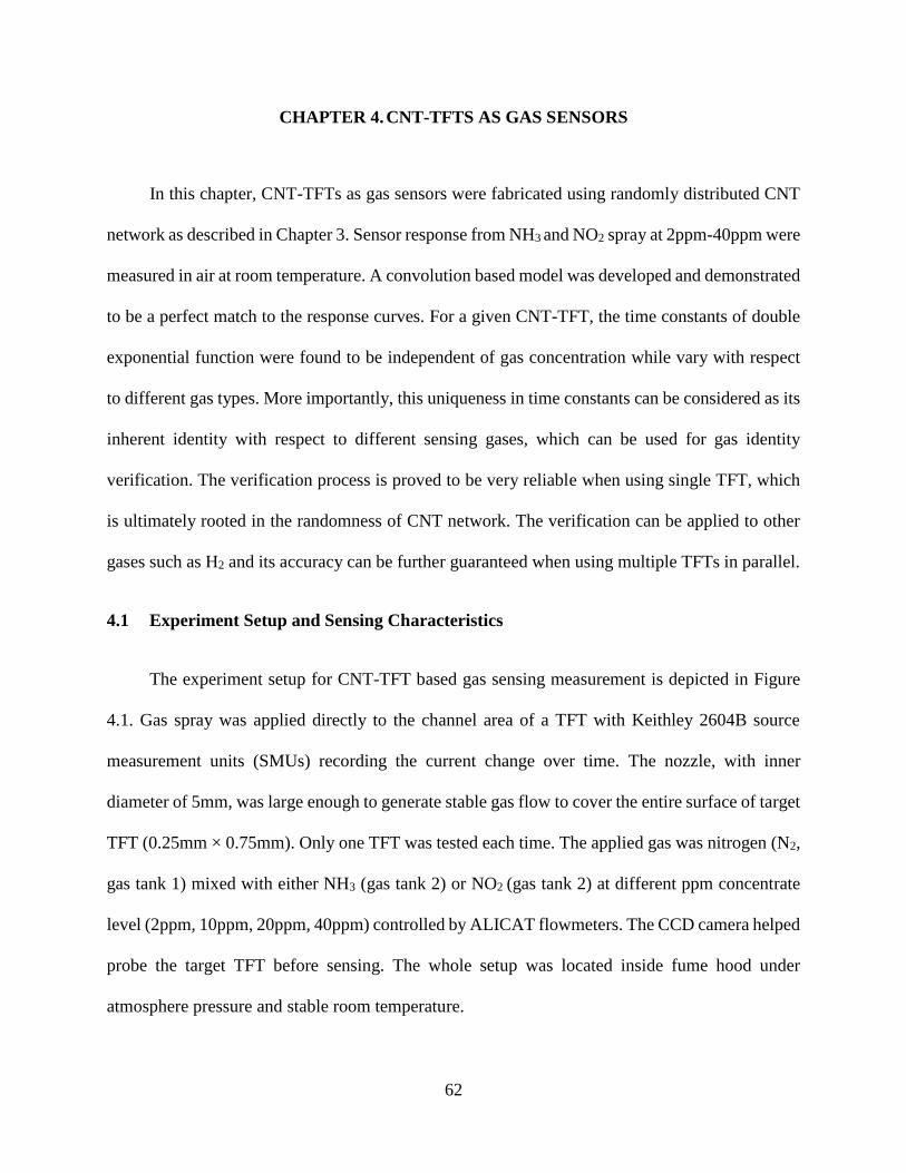
62
CHAPTER 4. CNT-TFTS AS GAS SENSORS
In this chapter, CNT-TFTs as gas sensors were fabricated using randomly distributed CNT
network as described in Chapter 3. Sensor response from NH3 and NO2 spray at 2ppm-40ppm were
measured in air at room temperature. A convolution based model was developed and demonstrated
to be a perfect match to the response curves. For a given CNT-TFT, the time constants of double
exponential function were found to be independent of gas concentration while vary with respect
to different gas types. More importantly, this uniqueness in time constants can be considered as its
inherent identity with respect to different sensing gases, which can be used for gas identity
verification. The verification process is proved to be very reliable when using single TFT, which
is ultimately rooted in the randomness of CNT network. The verification can be applied to other
gases such as H2 and its accuracy can be further guaranteed when using multiple TFTs in parallel.
4.1 Experiment Setup and Sensing Characteristics
The experiment setup for CNT-TFT based gas sensing measurement is depicted in Figure
4.1. Gas spray was applied directly to the channel area of a TFT with Keithley 2604B source
measurement units (SMUs) recording the current change over time. The nozzle, with inner
diameter of 5mm, was large enough to generate stable gas flow to cover the entire surface of target
TFT (0.25mm × 0.75mm). Only one TFT was tested each time. The applied gas was nitrogen (N2,
gas tank 1) mixed with either NH3 (gas tank 2) or NO2 (gas tank 2) at different ppm concentrate
level (2ppm, 10ppm, 20ppm, 40ppm) controlled by ALICAT flowmeters. The CCD camera helped
probe the target TFT before sensing. The whole setup was located inside fume hood under
atmosphere pressure and stable room temperature.

63
Figure 4.1 Schematic diagram of the experiment setup for gas sensing
During measurement, the target TFT was biased with Vds= - 0.5V and Vgs= - 1V. We first
apply this bias to the TFT for more than 20 minutes in order to stabilize the drain current (Id).
Then, we open the valves to release the gas mixture (either N2 + NH3 or N2 + NO2) while keep the
mass flowrate constant at 1000 sccm all the time. After 10 minutes of gas spray (gas on state), we
close the valves (gas off state) and keep the gas off state for 20~30 minutes before another sensing
cycle began at a higher ppm level. The lowest concentrate we used was 2ppm for both NH3 and
NO2 sensing, which is higher enough to get rid of the possible noise effect since the CNT-TFTs
might also detect interfering gases (such as NH3, NO2, H2, etc.) at ppb level from the environment.

64
Figure 4.2 2-cycle (2ppm and 40ppm) sensor response under NH3 or NO2 spray for a long
channel TFT (2K: W=100µm/L=80µm) and a short-channel TFT (2H: W=100µm/L=8µm).
Ro is the stable device resistance before gas spray. (a)-(b) Sensor response of 2K under NH3
or NO2 spray respectively. (c)-(d) Sensor response of 2H under NH3 or NO2 spray
respectively. Inset figures are the corresponding TFTs. Red curves are the fitting results
using common time constants of double exponential-convolution model.
4.2 Sample Characteristics and the Sensing Mechanism
The sensor response under 2-cycle (2ppm and 40ppm) of NH3 or NO2 pulsing is shown in
Figure 4.2 for a long-channel CNT-TFT with L=80µm/W=100µm (2K) and a short-channel CNT-
TFT with L= 8µm/W=100µm (2H). They all show stable sensor response to either NH3 or NO2
sensing. For each gas sensing process, the gas pulsing signal stayed for 10 minutes in ‘on state’
(shown as orange stripes for NH3 or green stripes for NO2 in figures) and 30 minutes in ‘off state’
(no stripe in figures) between each cycle. When NH3 molecules interact with the CNT network in
the channel area, they work as electron source which decreases the current by consuming the holes
in the channel of the p-type CNT-TFT. Thus, the resistance will increase during on state and

65
decrease during off state. NO2 affects the resistance in an opposite way by providing more holes
to the channel. For 2ppm concentration, both TFTs have more than 20% increase or decrease in
resistance when exposed to NH3 and NO2. While for 40ppm concentration, both TFTs show more
than 50% resistance decrease under NO2 spray and more than 40% resistance increase under NH3
spray.
From the sensor response curves, it is easy to find 4 phases within each gas spray cycle,
described in Figure 4.2(b) in bold green, which is vital to understand the sensing mechanism for
CNT-TFT based sensors. We define the interactive units between gas molecules and the device as
dwelling spots, which largely exist in CNT-CNT junctions, CNT-metal area, and other locations
such as defects on CNTs. A dwelling spot can either capture or release a gas molecule depending
on it is taken already or not.
For a gas spray cycle, phase 1 is the beginning of gas on state, where the resistance
experiences an abrupt change when large number of empty dwelling spots are being taken by the
gas molecules. Phase 1 only lasts for several seconds when all gas molecules can unlimitedly take
the empty spots, which counts for a significant proportion of the resistance change during the entire
on state. Even though gas molecules can escape their dwelling spots all the time, it can be ignored
compared to the amount of gas molecules that take the empty spots.
Phase 2 starts when a large number of the empty spots have already been taken. In this phase,
endless gas molecules reach the channel surface continuously like phase 1, but only part of them
can be taken by the dwelling spots because only some of them will reach unavailable spots, which
slows down the rate of change in resistance compared to phase 1. Another cause is, more and more
trapped molecules can escape their spots than phase 1. Even after saturation, the target TFT is in a

66
dynamic equilibrium with the escaping molecules cancelling out the molecules being taken by the
dwelling spots.
Phase 3 begins when gas spray comes to an end and no molecule reaches the channel surface
(gas off state). Conversely, there are a large number of gas molecules escaping their spots, resulting
in the abrupt change in resistance which is similar to phase 1 but in an opposite manner. In phase
4, the change rate slows down because it is more difficult for the remaining trapped molecules to
escape their spots. It is commonly known that the dwelling spots near CNT junctions and CNT-
metal region are much easier to capture gas molecules (gas molecules are relatively stable and
harder to escape in those spots) than CNT itself and other region of the channel. Therefore, the
slowness in phase 4 mainly results from the difficulty of gas molecules escaping from CNT
junctions and CNT-metal region, while the sudden change in resistance of phase 3 mainly
attributes to the rapid escape of gas molecules from CNT itself and other similar unstable gas-
dwelling spots.
4.3 Sensor Response Fitting
Enlightened by the two phases during gas on or gas off state, it is natural to resort to double
exponential function for fitting purpose. There are two formats related to double exponential
function
1( ) exp( / ) exp( / )a bf t a t b t = − + − (4.1)
2 ( ) exp( / ) exp( / )a bf t a t t b t t = − + − (4.2)

67
where τa and τb are time constants, t is time, a and b are constants. To distinguish these two formats,
we define equation 4.1 as double exponential function, equation 4.2 as double t exponential
function. The gas pulsing signal can be expressed as
( )
0
h gas ong t
gas off
=
(4.3)
where the constant h is the height of the pulse signal.
Rigoni et al. used convolution between double t exponential function and gas pulsing signal
to fit the sensor response curves of a whole cycle using the same time constants [50]. However,
we found convolution between double exponential function and gas pulsing signal is a better match
for our sensor response curves. To be specific, let D(t) be the original sensor response data, e.g.,
the sensor response curves in Figure 4.2. To fit D(t) separately for gas on state and gas off state in
each case, linear transformation was applied to move both gas on state and gas off state to the
origin from the onset point, exhibited in Figure 4.3(a). Obviously linear actions will not change
the time constants. Then we resorted to double exponential-convolution model to fit the sensor
response curves separately. That is
1 1( ) ( ) ( )
fD t f t g t= (4.4)
where 1( )
fD t is the fitting results from convolution between double exponential function and gas
pulsing signal. We consider a=1 to eliminate a redundant variable during fitting. Then apply linear
transformation for 1( )
fD t in order to restore the real time fitting
1( ) ( ) ( )
f f o oD t D t t D t= − + (4.5)

68
Where D(t) is the original sensor response data, to is the time at the onset point. The standard
deviation
υ = ‖𝐷𝑓(𝑡) − 𝐷(𝑡)‖ = √1
𝑁∑ (𝐷𝑓(𝑡𝑖) − 𝐷(𝑡𝑖))
2𝑁𝑖=1 (4.6)
is defined for error evaluation. Same process is applied for double t exponential-convolution model
by using f2 instead of f1.
Figure 4.3 Fitting for sensor response curves. (a) Linear transformation before fitting to
standardize the fitting process for different sensing gas. (b)-(c) Fitting result comparison of
device 2H in gas on and off state between double exponential-convolution (double exp)
model, double t exponential-convolution (double t exp) model, and quadratic model. (d)-(e)
Fitting result comparison of device 2K in gas on and off state between double exponential
and double t exponential models.

69
Table 4.1 Common time constants at different gas concentration in each state and the
corresponding fitting errors
Figure 4.3(b)-(c) compares the fitting results of 2H between double exponential-convolution
model, double t exponential-convolution model, and quadratic model. From the fitting curves,
double exponential-convolution model matches the original sensor response data the best in both
states. It is quite clear that the quadratic model is unable to depict the sudden change at the
beginning of each state (phase 1 and phase 3). While for double t exponential-convolution model,
the fitting is distorted during the transition period between each phase. Quantitatively, the standard
deviations (υ) for double exponential-convolution model, double t exponential-convolution model,
and quadratic model during gas on state are 3.65×10⁻⁵, 4.24×10⁻⁵, and 6.68×10⁻⁵ respectively. And
for gas off state, the corresponding standard deviations are 3.15×10⁻⁵, 4.31×10⁻⁵, and 4.55×10⁻⁵.
Therefore, double exponential-convolution model can best fit the sensor response curves. Figure
4.3(d)-(e) further confirm the superior of double exponential-convolution model. Other fitting
cases also support the same conclusion.

70
Figure 4.4 4-cycle (2ppm, 10ppm, 20ppm, 40ppm) sensor response and the corresponding
fitting, using common time constants of double exponential-convolution model at different
gas concentration. (a)-(b) Results for a long channel device 3F. (c)-(d) Results for a short
channel device 3A.
4.4 Consistency of Time Constants for Different Concentration
During sensor response fitting from double exponential-convolution model, we noticed the
two time constants (τa and τb) in equation 4.1 are quite stable for sensing at different gas
concentrations. Based on that observation, we assumed the same τa and τb (common time constants)
while fitting response of the same TFT during gas sensing at different concentrations. The fitting
results are shown in Figure 4.2. The common time constants and the corresponding fitting errors
are listed in Table 4.1. Surprisingly, the fitting are excellent for both NH3 and NO2 spray in either
gas on state or gas off state. Figure 4.4 shows the fitting results for another TFT at 4 different gas
concentrations, which are 2ppm, 10ppm, 20ppm, and 40ppm. The excellence in sensor response
fitting from both Figure 4.2 and Figure 4.4 demonstrates the consistency of the common time
constants with respect to different gas concentration.
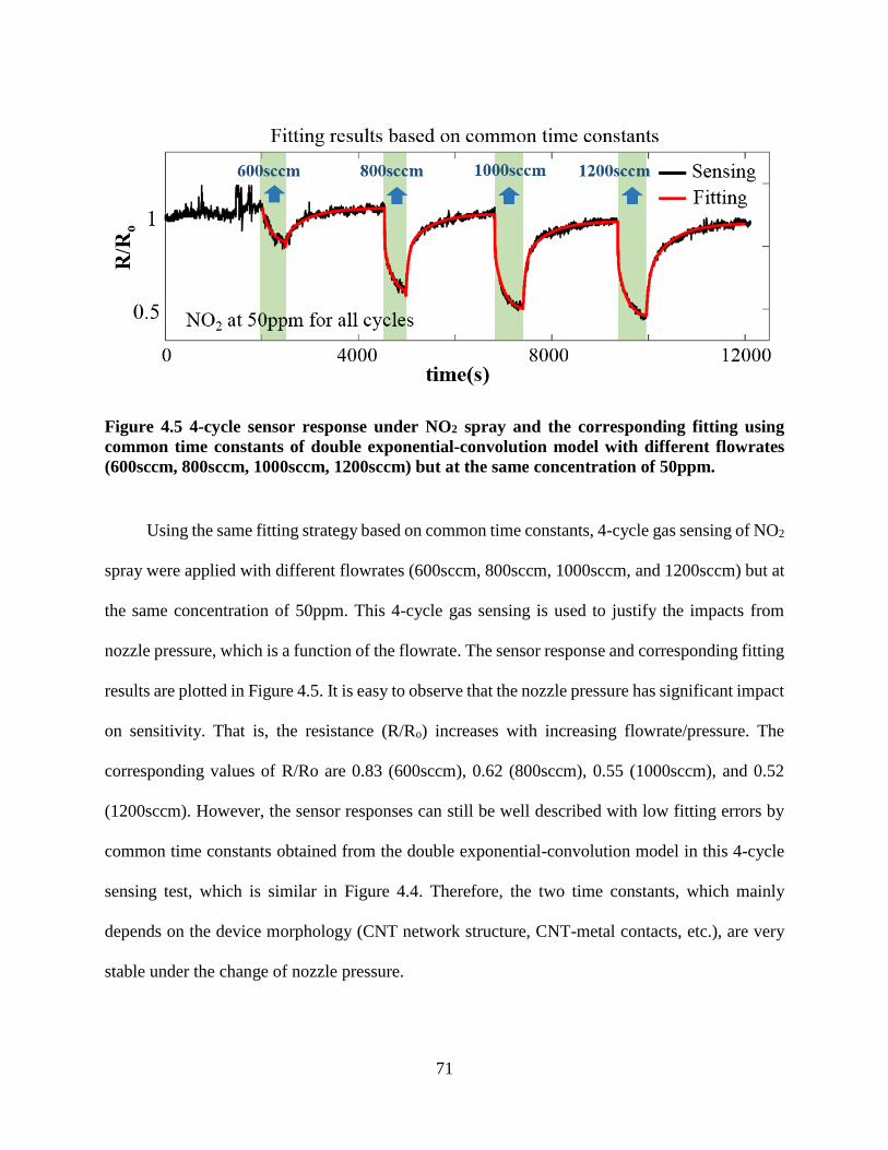
71
Figure 4.5 4-cycle sensor response under NO2 spray and the corresponding fitting using
common time constants of double exponential-convolution model with different flowrates
(600sccm, 800sccm, 1000sccm, 1200sccm) but at the same concentration of 50ppm.
Using the same fitting strategy based on common time constants, 4-cycle gas sensing of NO2
spray were applied with different flowrates (600sccm, 800sccm, 1000sccm, and 1200sccm) but at
the same concentration of 50ppm. This 4-cycle gas sensing is used to justify the impacts from
nozzle pressure, which is a function of the flowrate. The sensor response and corresponding fitting
results are plotted in Figure 4.5. It is easy to observe that the nozzle pressure has significant impact
on sensitivity. That is, the resistance (R/Ro) increases with increasing flowrate/pressure. The
corresponding values of R/Ro are 0.83 (600sccm), 0.62 (800sccm), 0.55 (1000sccm), and 0.52
(1200sccm). However, the sensor responses can still be well described with low fitting errors by
common time constants obtained from the double exponential-convolution model in this 4-cycle
sensing test, which is similar in Figure 4.4. Therefore, the two time constants, which mainly
depends on the device morphology (CNT network structure, CNT-metal contacts, etc.), are very
stable under the change of nozzle pressure.

72
Figure 4.6 Gas identification based on common time constant and the corresponding error
difference. (a) Fitting results from different gas assumptions (time constant pairs) for device
2K in gas on state. (b) Same strategy as (a) for device 2K in gas off state.
4.5 Gas Identification
For a given CNT-TFT, the two time constants, (τa , τb) pair, are unique for either gas on state
or gas off state and do not depend on the gas concentration. More importantly, (τa , τb) pair changes
with respect to different gas types. Therefore, the one-to-one mapping between time constants and
gas types can be regarded as the inherent properties for a given TFT, which can be used for gas
identity verification depend on the corresponding error difference.
Take the device 2K in Figure 4.2(a) as an example, (τa , τb) pair for different gas sensing in
different states can be determined easily from tentative testing for calibration purpose, shown in
Table 4.1. For an unknown sensing gas (e.g., either NH3 or NO2), let 2K record the sensor response
for a cycle. Based on (τa , τb) pairs from different assumptions, the corresponding fitting errors can

73
be obtained, shown in Figure 4.6. It is clear that (τa , τb)=(471, 5.0) from NH3 assumption can
perfectly fit the sensor response curve while the fitting is distorted when (τa , τb)=(227, 10.9) from
NO2 assumption. Quantitatively, the fitting error is υ=3.22×10⁻⁵ when (τa , τb)=(471, 5.0) during
gas on state, while υ=17.57×10⁻⁵ when (τa , τb)=(227, 10.9). That means the fitting error from NO2
assumption is more than 5 times larger than NH3 assumption. Therefore, we can safely conclude
the unknown gas is NH3, not NO2. Same conclusion can be drawn from the corresponding error
difference during gas off state, shown in Figure 4.6. Without any doubt, this is actually a general
strategy that can be easily applied for identity verification for more gases. Moreover, this gas
identification strategy is proved to be valid for gas sensing with different flowrates (different
nozzle pressure), which is confirmed by conducting sensing test with different flowrates ranging
from 600sccm to 1200sccm.
Figure 4.7 The cycling sensing experiment and comparison of the corresponding sensor
responses under NO2 spray at the same concentration (20ppm) for the same device at 5
hours’ time period. Fitting 1 is based on common time constants and fitting 2 is based on
separate time constants.

74
The cycling experiment has been conducted under NO2 spray at the same concentration
considering possible external influence (e.g., humidity, temperature fluctuation, other possible
sensing noise) during sensing test at different time. The corresponding sensor responses are plotted
in Figure 4.7 at 5 hours’ time difference. During this period, the target sensor is put in air in order
to ensure the full interaction with surrounding environment for enough time. Fitting 1 is based on
common time constants and fitting 2 is based on separate time constants (performed separately for
each cycle, which is the best fitting from the convolution model). As shown in Figure 4.7, the
overall errors from fitting 2 are 2.26×10⁻⁵ and 6.94×10⁻⁵ in gas on and gas off state respectively.
As for fitting 1, those values are 3.11×10⁻⁵ and 9.22×10⁻⁵, which means the changes are only 138%
and 132% between fitting 1 and fitting 2. However, the error difference between different gas
assumptions (NH3 and NO2) is as large as 10 times (1000%) for gas identification. Therefore, the
external influence is very limited, which will not affect the accuracy of gas identification.
Theoretically, this identification process can be conducted through only one state from a
single sensing cycle because of the uniqueness of (τa ,τb) pair. Figure 4.8 maps the (τa ,τb) pairs for
more TFTs under NH3 and NO2 spray. The scattered marks reveal the uniqueness of (τa ,τb) pair
with respect to different gas types for different TFTs. On the one hand, for a given TFT, there is
no overlapped or even close (τa ,τb) pairs with respect to different gases. On the other hand, for a
given sensing gas, there is no overlapped or even close (τa ,τb) pairs with respect to different TFTs
either. This uniqueness mainly roots in the randomness of CNT network inside the channel area,
which is different with respect to CNT network density, CNT network structure, and channel
dimensions, etc.

75
Figure 4.8 One-to-one mapping for time constant pairs (τa ,τb) in gas on state (a) and gas off
state (b). The same marks denote the same gas type, and the same colors represent the same
device.
However, in practice, some (τa, τb) pairs might be very close to each other and cause
interference when considering sensing cases for more possible gases. Many causes contribute to
this such as ambience noise, unstable gas spray, experimental errors, etc. To address this problem,
more tentative testing for a better calibration is vital in order to obtain the authentic time constant
pairs for each gas sensing case. Similarly, performing multiple sensing cycles are also crucial
during identity verification process. More efficiently, different TFTs can be used in parallel for
gas identification instead of using just one, which helps avoid the possibility that the difference in
fitting errors might be on the same level. Generally, the smoother sensor response from longer

76
channel TFTs are more reliable for gas identification because of the larger difference in fitting
errors. From most cases we experienced, one TFT is enough for the verification process.
4.6 Closure
CNT-TFT based gas sensors have been fabricated with randomly distributed CNT network
and sensor response under NH3 and NO2 spray at low ppm level have been tested. The different
phases for gas response within each cycle suggest the sensing mechanism is based on the
interaction between gas molecules and different types of dwelling spots inside the device. We
developed double exponential-convolution model to fit the sensor response. The two time
constants of double exponential function are found to be independent of gas concentration, but
vary with respect to different gas types and different TFTs. This can be used for gas identification
because of the uniqueness of the time constants for different gas types. We ascribe this uniqueness
to the randomness of CNT network in channel area, which help build a unique channel structure
for each TFT and thus create the diversity in dwelling spots for gas molecules during sensing
process. By comparing the large difference in fitting errors, this one-to-one dependence between
time constants and the sensing gases is successfully used for gas identity verification between NH3
and NO2. More significantly, it actually provides a general and practical strategy for identity
verification over more gases without distinction. In perspective, this analysis manages to create
the selectivity of SWCNT based sensors with respect to different gases, which will largely broaden
their applications in practice.
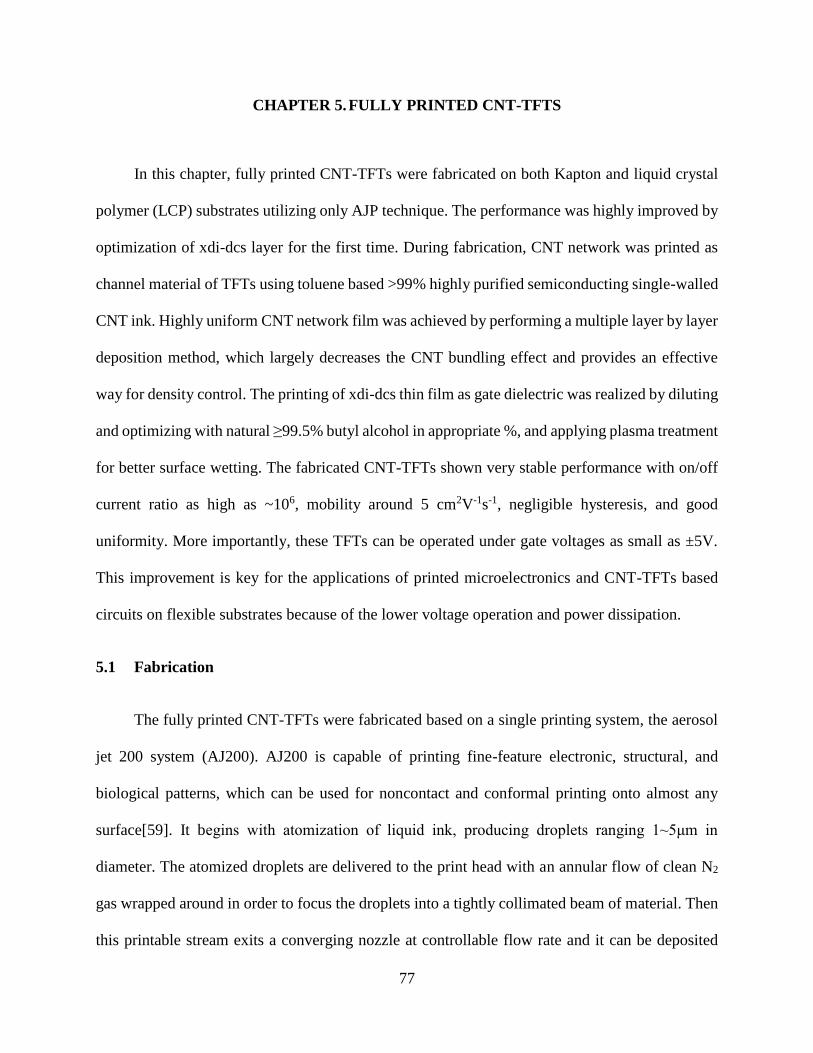
77
CHAPTER 5. FULLY PRINTED CNT-TFTS
In this chapter, fully printed CNT-TFTs were fabricated on both Kapton and liquid crystal
polymer (LCP) substrates utilizing only AJP technique. The performance was highly improved by
optimization of xdi-dcs layer for the first time. During fabrication, CNT network was printed as
channel material of TFTs using toluene based >99% highly purified semiconducting single-walled
CNT ink. Highly uniform CNT network film was achieved by performing a multiple layer by layer
deposition method, which largely decreases the CNT bundling effect and provides an effective
way for density control. The printing of xdi-dcs thin film as gate dielectric was realized by diluting
and optimizing with natural ≥99.5% butyl alcohol in appropriate %, and applying plasma treatment
for better surface wetting. The fabricated CNT-TFTs shown very stable performance with on/off
current ratio as high as ~106, mobility around 5 cm2V-1s-1, negligible hysteresis, and good
uniformity. More importantly, these TFTs can be operated under gate voltages as small as ±5V.
This improvement is key for the applications of printed microelectronics and CNT-TFTs based
circuits on flexible substrates because of the lower voltage operation and power dissipation.
5.1 Fabrication
The fully printed CNT-TFTs were fabricated based on a single printing system, the aerosol
jet 200 system (AJ200). AJ200 is capable of printing fine-feature electronic, structural, and
biological patterns, which can be used for noncontact and conformal printing onto almost any
surface[59]. It begins with atomization of liquid ink, producing droplets ranging 1~5μm in
diameter. The atomized droplets are delivered to the print head with an annular flow of clean N2
gas wrapped around in order to focus the droplets into a tightly collimated beam of material. Then
this printable stream exits a converging nozzle at controllable flow rate and it can be deposited
78
onto the target surface with relatively high velocity. The printed features can reach small width
around 10μm and thickness of submicron level, which are also determined by the ink properties
and surface conditions. The whole printing process needs no vacuum or pressure chambers and it
can operate under room temperature. Generally, no substrate damage will occur despite the high
velocity of the stream.
Figure 5.1 Schematic of fabrication process of fully printed CNT-TFTs on flexible substrates
using AJP. (a) A well prepared flexible substrate (either Kapton or LCP) which is cleaned
by 3-5min oxygen plasma before printing. (b) Ag printing as S/D electrodes. (c) 1min oxygen
plasma before CNT printing for better wetting. (d) CNT network printing using a multiple
layer by layer printing method. (e) Dielectric layer/xdi-dcs printing. (f) 2-3min oxygen
plasma treatment before Ag printing. (g) Ag printing as a top gate electrode. A fully printed
CNT-TFT is fabricated by this process. Note: Ag is cured at 150°C for 15~25min. Dielectric
layer/xdi-dcs is cured at 140°C for 20min.
5.1.1 Fabrication Process
The fabrication process of the fully printed CNT-TFTs using AJP technique is shown in
Figure 5.1. During fabrication, Kapton (DuPont, USA) and LCP (Rogers, USA) films were used
as the flexible substrates. They were rinsed by acetone, IPA, and DI water successively, then blown
dry by N2 gun. Next, 5min oxygen plasma was applied for better surface preparation. Followed by

79
Ag printing (Ag ink: UTD Ag Conductive Silver Nanoinks, UT Dot) as source and drain (S/D)
electrodes using AJ200. Then Ag patterns are cured at 150°C for 15~25min in an oven. Before
CNT printing (CNT ink: IsoSol-S100® Polymer-Wrapped Nanotubes, NanoIntegris), 30s quick
oxygen plasma was applied to functionalize the surface which could help achieve uniformly
distributed CNT network. A thorough cleaning of AJ200 would be indispensable when changing
from Ag to CNT ink (2~3hours ultrasonic, then acetone, IPA, DI water, and toluene rinse
successively). After CNT printing, toluene rinse was used to wash away the excess surfactant and
polymers on the surface, followed by thermal annealing at 120°C for >1hour in the oven. After
that, xdi-dcs thin layer was printed (with sheath gas flow rate of 40CCM and printing speed of
10mm/s for all as default setting) as gate dielectric (xdi-dcs ink: Xerox Research Center Canada),
which was diluted and optimized with butyl alcohol (Sigma Aldrich), cured by thermal annealing
at 140°C for 20min in the oven. Then 2-3min oxygen plasma was performed to make the surface
of the xdi-dcs layer hydrophilic before Ag printing again as gate electrodes on top, followed by
Ag cure at 150°C for 15~25min. Ultrasonic atomizer is good enough for the printing of all inks
involved. The sheath gas flow rate (SG), ultrasonic atomizer flow rate (UA), and printing speed
(PS) are chosen differently to control the printing quality with respect to different inks.
5.1.2 Fabrication Details
Printing Ag Electrodes:
The Ag ink is based on silver nanoparticles with average size around 10 nm and dispersed
in a liquid vehicle. Since they are surface stabilized, UTD’s Ag inks are highly soluble in nonpolar
organic solvents and stable under atmospheric conditions at room temperature. The ink is tuned

80
by using xylene as solvent for better printing quality. The prepared ink was printed on flexible
substrate such as Kapton and LCP.
A 100μm diameter nozzle was used for Ag printing. SG, UA, and PS were set to 25CCM,
18CCM, 10mm/s respectively in most of the cases (PS=10mm/s was set as default value for all
Ag, CNT, and xdi-dcs printing unless stated otherwise). SG and UA changes in the range of 15-
30CCM and 15-25CCM accordingly for Ag printing, depending on the tuning degree by using
xylene as solvent. SG and UA also affect the printing quality of Ag. Generally, the increase of SG
will decrease the width and increase the height of each printed Ag line. Ag can be cured at 150°C
for 30min or 180°C for 10min in ambient. One-layer printing is enough for all the Ag patterns of
the CNT-TFTs. The thickness of printed Ag patterns changes between 0.6-1.5μm with average of
~0.8μm, measured by Tencor P15 profilometer.
The temperature of chilling water bath and the platen was maintained at 25 °C and 75 °C
respectively (for the printing of Ag, CNT, and xdi-dcs). 3-5min oxygen plasma before Ag printing
will be very helpful to clean the surface of the substrates and ensure better wetting during printing.
Printing CNT Network:
Highly purified (>99% semiconducting) single-walled CNT solution are used as printable
inks for CNT network. The initial concentration of the solution is 0.05 mg/mL and was further
diluted with toluene at volumetric ratio of 1:1 before printing.
A 150μm diameter nozzle was used for CNT printing with SG=40CCM, UA=40CCM, and
PS=10mm/s in most of the cases. UA changes between 30-45CCM based on the dilute ratio as
well as the stability of the AJP system (CNT and xdi-dcs printing is more sensitive than Ag
81
printing). After printing, the samples were rinsed with toluene to remove excess surfactant,
followed by thermal annealing in air at 140 °C for an hour. For multiple layer by layer deposition
of CNT network, the processes of CNT printing, toluene rinse, and thermal annealing were
performed 2-4 times under same conditions for both network density control and better uniformity.
Before CNT printing, the system needs to be cleaned thoroughly by using 2 hours ultrasonic
bath, followed by acetone, IPA, and DI water rinse successively. It can avoid contamination of
CNT ink because it is very sensitive to the tube and assembly system. Again, 1min oxygen plasma
will be helpful before CNT printing in order to reduce the bundling effect of CNTs. However,
oxygen plasma can partially oxidize the previously printed Ag pattern, which will darken the
overall color conspicuous. But result shows this oxidization only has limited influence on the
conductivity of Ag patterns. No extra plasma should be appplied during multiple layer by layer
CNT network deposition because it can easily etch away CNTs.
Printing xdi-dcs:
The original dielectric ink, xdi-dcs, is formed by mixing poly(vinylphenol) and poly(methyl
silsesquioxane) in a ratio of 10:1. It is diluted and well optimized by using natural ≥99.5% butyl
alcohol (Sigma Aldrich Inc.) to reach thinner printing for better quality with volumetric dilute ratio
σ around 1:2.5 (xdi-dcs : butyl alcohol).
A 150μm diameter nozzle was used for xdi-dcs printing with SG=18CCM, UA=30CCM,
PS=10mm/s in order to achieve thickness of ~0.3μm. The value of UA can be adjusted between
30CCM and 38CCM to control the thickness of xdi-dcs thin film ranging from 0.3-0.8μm
accordingly. After printing, xdi-dcs is cured at 140 °C for 30min.
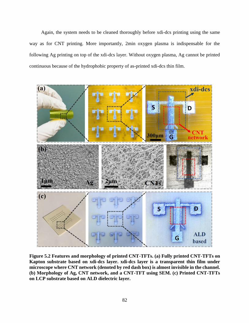
82
Again, the system needs to be cleaned thoroughly before xdi-dcs printing using the same
way as for CNT printing. More importantly, 2min oxygen plasma is indispensable for the
following Ag printing on top of the xdi-dcs layer. Without oxygen plasma, Ag cannot be printed
continuous because of the hydrophobic property of as-printed xdi-dcs thin film.
Figure 5.2 Features and morphology of printed CNT-TFTs. (a) Fully printed CNT-TFTs on
Kapton substrate based on xdi-dcs layer. xdi-dcs layer is a transparent thin film under
microscope where CNT network (denoted by red dash box) is almost invisible in the channel.
(b) Morphology of Ag, CNT network, and a CNT-TFT using SEM. (c) Printed CNT-TFTs
on LCP substrate based on ALD dielectric layer.

83
Figure 5.3 The effects of oxygen plasma treatment before CNT network printing (a)-(f) and
Ag printing on top of xdi-dcs thin film (g)-(h). Without plasma treatment, CNTs bundle
together easily (a)-(b) and Ag thin film is uneven with huge pinholes everywhere (g). CNT
network density can be well controlled by multiple layer by layer deposition after plasma
treatment (c)-(f). Scale bar is 2μm in each figure.
5.2 Morphologies and Performance
Figure 5.2 describes the structure and SEM images of the printed CNT-TFTs. Figure 5.2(a)
displays fully printed CNT-TFTs using xdi-dcs as gate dielectric. For comparison, CNT-TFTs with
~80nm aluminum oxide (Al2O3) layer as gate dielectric were fabricated using ALD at 100°C,
replacing the xdi-dcs layer for new CNT-TFTs (ALD based CNT-TFTs), depicted in Figure 5.2(c)
(the rest fabrication steps are the same). CNT network is printed on top of S/D electrodes, which
is proved to have better contact than S/D on top of CNT network[61]. Top gate is used in the CNT-

84
TFTs to achieve lower hysteresis of the devices, where CNT network is not in direct contact with
the environment. The morphology of the CNT-TFTs (as-printed Ag, CNT network, and xdi-dcs)
on flexible substrates can be seen in Figure 5.2(b). CNT network is only visible by using SEM.
Figure 5.2(b)-middle shows uniform CNT network resulting from multiple layer by layer
deposition method. In order to acquire highly uniform CNT network, CNT printing, toluene
rinsing, and blown dry processes (1 cycle altogether) are performed repeatedly for density control
(normally 2-4 cycles).
Figure 5.4 I-V characteristics of CNT-TFTs. Transfer curve (a) and output curve (b) of
printed CNT-TFTs where gate dielectric were fabricated using ALD (~80nm Al2O3,
W=500μm, L=100μm, 1-cycle CNT network deposition). Transfer curve (c) and output curve
(d) of a fully printed CNT-TFTs based on printed dielectric layer with thickness as small as
0.3μm (W=500μm, L=100μm, 3-cycle CNT network deposition).

85
The significance of oxygen plasma treatment and multiple layer by layer deposition of CNT
network can be seen in Figure 5.3. Without oxygen plasma treatment, CNTs bundle together easily
as shown in Figure 5.3(a) and 5.3(b). And multiple layer by layer deposition cannot result in
uniform CNT network because CNTs tend to entangle to the previously printed CNTs which
makes the bundling effect even worse. Multiple layer by layer deposition works very well after
1min plasma treatment before printing as observed in Figure 5.3(c)-5.3(f), where CNT network
density can be controlled by performing multiple cycles as needed. Similar effect can be expected
for Ag printing on top of xdi-dcs thin film because of the hydrophobic property of the as-printed
xdi-dcs layer, shown in Figure 5.3(g) and 5.3(h).
The I-V characteristics of the CNT-TFTs was measured using Microtech Summit 11 k probe
station and Keithley 4200 SCS. We fabricated series of devices with the same channel width
(W=500μm), but different channel lengths (L=50~250μm). The output characteristics (Id−Vds
curves) and transfer characteristics (Id−Vgs curves) of the CNT-TFTs are plotted in Figure 5.4.
Figure 5.4(a) and 5.4(b) are ALD based CNT-TFTs, Figure 5.4(c) and 5.4(d) are fully printed
CNT-TFTs. The on/off ratio of the fully printed CNT-TFTs ranges from 103 to 106, which
increases with increasing channel length. The overall I–V characteristics shows good p-type
performance with mobility ranging from 2 to 8 cm2V-1s-1.
5.3 Optimization of Printed xdi-dcs Thin Film
The performance of fully printed CNT-TFTs is mainly limited by the gate dielectric. The
printing of xdi-dcs thin film is critical to obtain relatively high-performance CNT-TFTs. During
AJP printing, the thickness of xdi-dcs can vary in large range based on the dilute ratio of xdi-dcs
as well as the printing parameters such as SG, UA, and PS. The thinnest xdi-dcs film we achieved

86
for a CNT-TFT is ~0.3μm (SG=18CCM and PS=10mm/s as default setting unless stated otherwise,
UA=30CCM in this case), and the thickest could be larger than 1μm (measured by Tencor P15
profilometer). Figure 5.5 displays the difference in transfer characteristics caused by the thickness
of xdi-dcs thin film. The difference in thickness is controlled by the values of UA, which are
30CCM, 32CCM, 36CCM, and 40CCM for 0.33μm, 0.41μm, 0.59μm, and 0.91μm respectively.
Except for the values of UA, the fabrication process and other parameters/dimension are exactly
same for the CNT-TFTs (W=500μm, L=100μm, 2-cycle CNT network deposition).
Figure 5.5 The impact of the printed xdi-dcs layer on the performance of fully printed CNT-
TFTs. (a) Comparison of transfer curves of four fully printed CNT-TFTs with different
thickness of dielectric layers. (b) The dependence of Vth on the thickness of printed xdi-dcs
thin films for fully printed CNT-TFTs.
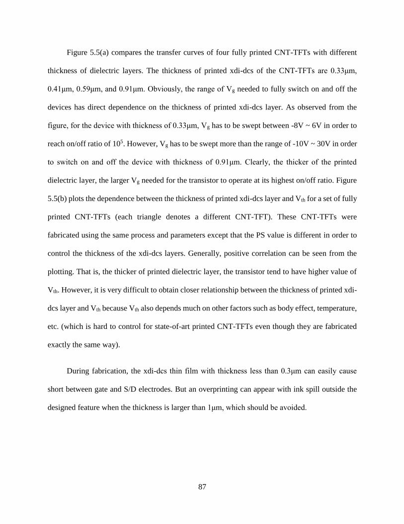
87
Figure 5.5(a) compares the transfer curves of four fully printed CNT-TFTs with different
thickness of dielectric layers. The thickness of printed xdi-dcs of the CNT-TFTs are 0.33μm,
0.41μm, 0.59μm, and 0.91μm. Obviously, the range of Vg needed to fully switch on and off the
devices has direct dependence on the thickness of printed xdi-dcs layer. As observed from the
figure, for the device with thickness of 0.33μm, Vg has to be swept between -8V ~ 6V in order to
reach on/off ratio of 105. However, Vg has to be swept more than the range of -10V ~ 30V in order
to switch on and off the device with thickness of 0.91μm. Clearly, the thicker of the printed
dielectric layer, the larger Vg needed for the transistor to operate at its highest on/off ratio. Figure
5.5(b) plots the dependence between the thickness of printed xdi-dcs layer and Vth for a set of fully
printed CNT-TFTs (each triangle denotes a different CNT-TFT). These CNT-TFTs were
fabricated using the same process and parameters except that the PS value is different in order to
control the thickness of the xdi-dcs layers. Generally, positive correlation can be seen from the
plotting. That is, the thicker of printed dielectric layer, the transistor tend to have higher value of
Vth. However, it is very difficult to obtain closer relationship between the thickness of printed xdi-
dcs layer and Vth because Vth also depends much on other factors such as body effect, temperature,
etc. (which is hard to control for state-of-art printed CNT-TFTs even though they are fabricated
exactly the same way).
During fabrication, the xdi-dcs thin film with thickness less than 0.3μm can easily cause
short between gate and S/D electrodes. But an overprinting can appear with ink spill outside the
designed feature when the thickness is larger than 1μm, which should be avoided.

88
Figure 5.6 (a) Schematic structure (layer by layer structure and the sectional view) used to
test the insulation quality of printed xdi-dcs thin films. (b) Visualization of printed xdi-dcs
thin film at different dilute ratio σ and UA. The devices in upper figures will not work as
numerous pinholes created during xdi-dcs printing. The middle figures show well printed
xdi-dcs thin films. The lower figures will not work either because of the over printing, which
can result in several big pinholes (denoted by red dash area, left) and even ruin the substrate
(right).
Even though thin xdi-dcs layer is the key for fully printed CNT-TFTs, it can hardly go
thinner than 0.3μm because the existence of pinholes in an extremely thin film (<0.3μm) can easily
cause short circuit (pinhole effect, which fails to provide good insulation between gate and S/D
electrodes).

89
Figure 5.6(a) illustrates the structure we used to test the insulation quality of printed xdi-dcs
thin film, which is similar to the structure of fully printed CNT-TFTs. Undoubtedly, good
insulation of printed dielectric is the precondition for fully printed CNT-TFTs. The measured
capacitance of printed xdi-dcs thin film is 6-8 nF/cm2 with thickness between 0.3-0.8μm.
Generally, bad quality of xdi-dcs layer results from severe pinhole effect when current can flow
directly from the red Ag electrode (gate) to the black Ag electrodes (S/D) of Figure 5.6(a).
To optimize the printing quality of xdi-dcs layer, natural ≥99.5% butyl alcohol is used to
dilute the xdi-dcs ink with dilute ratio σ (defined as volumetric ratio of xdi-dcs : butyl alcohol)
ranging from 1:1 to 1:4. Figure 5.6(b) shows the printed xdi-dcs layers at different σ and UA,
which are the two most important parameters for printed xdi-dcs thin film. As shown in the figures,
when σ is 1:1 or less dilution, no continuous thin layer can form. Instead, the printed features show
particle-like morphology with numerous small pinholes. When σ is 1:4 (or further dilution), the
morphology of printed features is severely uneven with several large pinholes (red dash area).
Worse still, when UA is as large as 35CCM, over spill of the ink from the nozzle will ruin the
substrate badly (over printing). Clearly, over printing of xdi-dcs can cause troubles too. In general,
good morphology of printed features can be achieved with σ around 1:2.5, which results in very
uniform and continuous xdi-dcs thin film and the thickness can be well controlled by changing UA
accordingly.
Based on the structure displayed in Figure 5.6(a), 5 samples are fabricated for each
combination of σ and UA, with σ varying from 1:1 to 1:4 and UA varying from 22CCM to 42CCM.
The yield counts the number of samples without short between the red Ag electrode and the two
black Ag electrodes while using printed xdi-dcs thin film.

90
Figure 5.7 Optimization of printed xdi-dcs thin film. (a) Yield rate (number of samples with
good insulation quality) under different σ and UA combinations. (b) Thickness dependence
of xdi-dcs thin film on UA when σ equals to 1:2.5, which is the best σ from (a). The black
dash box in (a) and (b) denotes UA range of 30-38CCM at best σ.
The results can be seen in Figure 5.7(a). The samples with good insulation quality are 0/30,
2/30, 4/30, 16/30, 12/30, 2/30, 0/30 when σ equals to 1:1, 1:1.5, 1:2, 1:2.5, 1:3, 1:3.5, 1:4
respectively with UA changing from 22 to 42CCM for each σ. Similarly, those values are 0/30,
0/30, 7/30, 13/30, 11/30, 5/30 when UA equals to 22, 26, 30, 34, 38, 42CCM respectively with σ
changing from 1:1 to 1:4 for each UA. Therefore, (σ, UA) = (1:2.5, 34), would be one of the best
91
combinations for the printing of xdi-dcs thin film. Other combinations such as (σ, UA) = (1:2.5,
38) and (σ, UA) = (1:3, 34) are also very reliable in the test.
The value of σ is more important because it cannot be adjusted freely during printing, which
should be determined before printing. Figure 5.7(b) plots the thickness dependence on UA of
printed xdi-dcs thin film when σ is determined as 1:2.5 in advance. UA can be changed freely as
needed during printing. To guarantee the stability of the ink mist of xdi-dcs, the printing is
performed 2min after the changing of UA value. The time interval for each printing cycle (1st cyle,
2nd cycle, and 3rd cycle) is roughly 1 hour. Generally, the dependence in Figure 5.7(b) should be
linear because of mass conservation. However, the printing becomes unstable when UA>40CCM
(σ=1:2.5). Worse still, over printing can happen when UA is close to 50CCM , which is similar as
depicted in Figure 5.6(b) when (σ, UA)=(1:4, 35). The instability and over printing (UA>40CCM
at σ=1:2.5) make the curve deviate from linear dependence, which should be avoided for better
printing quality. Therefore, the data inside the black dash box of Figure 5.7(b) has more
significance because of the high reliability and the high yield rate which can be seen from Figure
5.7(a). Collectively, the printing of xdi-dcs thin film can be well optimized to achieve thickness as
thin as ~0.3μm by using AJP and the corresponding devices can be operated using gate voltages
as small as ±5V. High printing quality of the dielectric layer is the key for fully printed CNT-TFTs
with much lower power dissipation.
5.4 Closure
Using only AJP, fully printed CNT-TFTs have been fabricated on flexible substrates. The
fabricated devices can be fully switched on and off by using Vg as small as ±5V to reach on/off
ratio as high as ~106. During printing, multiple layer by layer deposition method is applied for

92
CNT network. The advantages lie in the density control as well as highly uniform CNT network
structure. By diluting xdi-dcs with natural ≥99.5% butyl alcohol in appropriate volumetric ratio
(σ=1:2.5), printed dielectric thin film with thickness of ~0.3μm can be achieved with high yield
rate for fully printed CNT-TFTs. The high quality of printed dielectric layer free of pinhole effect
can be achieved by controlling the UA. The improvement in printed dielectric layer is crucial for
flexible transistors with lower voltage operation and power dissipation, which paves the path for
applications of CNT-FETs as building blocks in wearable and bendable devices such as flexible
displays, RFID antennae/tags, sensors, artificial skins, etc.
93
CHAPTER 6. FULLY PRINTED GAS SENSORS
In this chapter, CNT gas sensors were fabricated using three different methods:
photolithography (PL), aerosol jet printing (AJP), and low-cost inkjet printing (IJP) (Epson C88+
and Epson Artisan 1430) and compare their performance in context of sensitivity and variability.
The latter two were fully printed sensors on flexible substrates (Kapton or PET). The sensor
responses of all the CNT sensors (referred as PL sensors, AJP sensors, IJP sensors respectively)
were obtained for the detection of reducing gas NH3 and oxidative gas NO2. The measurement was
conducted at low ppm level in air at room temperature. AJP sensors and IJP sensors showed high
sensitivity and stability in performance, with no obvious disadvantages compared to PL sensors.
During fabrication, both drop-cast and printed CNT network were patterned for the sensors,
resulting in bundled CNT network and highly uniform CNT network, respectively. The sensitivity
was surprisingly high for some printed CNT sensors with drop-cast CNT network. Moreover, the
post drop-cast deposition could help improve the sensitivity by rebuilding the CNT network of low
sensitivity sensors, which implies the potential of fabrication of extremely low-cost CNT gas
sensors using IJP with drop-cast method.
6.1 Fabrication
Fully printed AJP sensors, using CNT networks as sensing element, were fabricated using
Optomec Aerosol Jet 200 system (AJ200). The fabrication process is illustrated in Figure 6.1(a).
A flexible substrate of Kapton (DuPont) was cleaned by acetone, IPA, and DI water, and then
blown dry by nitrogen gun. After that, a surface treatment was performed using oxygen plasma,
which ensured better wetting between Ag and the substrate. For printing Ag, 100μm size nozzle
was utilized to pattern the electrodes with channel width (W) of 500μm and channel length (L) in

94
the range of 100~250μm. Ag was cured by thermal annealing at 150°C for ~20min in an oven.
Next, 30s oxygen plasma was applied to functionalize the surface, followed by CNT printing using
150μm size nozzle. In order to acquire highly uniform CNT network, after each layer of CNT
printing, toluene rinsing, and blown dry processes (1 cycle) were performed; this process is
repeated for CNT density control (normally 2~4 cycles, the multiple layer by layer deposition
method). At last, the entire device was put in the oven at 120°C for 30min.
Figure 6.1 Fabrication steps of AJP sensors (a) and highly simplified fabrication steps of IJP
sensors (b). For IJP, extremely low-cost daily-used printers (Epson C88+ or Artisan 1430)
were utilized without any controllable stage.
For fully printed IJP sensors, the process was highly simplified in order to demonstrate a
very low-cost fabrication process. As shown in Figure 6.1(b), flexible mesoporous PET substrates
were prepared the same way as for AJP. Then, Ag electrodes with L=500~1000μm and effective
W >10mm were printed using very low-cost printer Epson C88+ ($108) or Artisan 1430 (~$300)
without oxygen plasma treatment. These printers have < 1% price of frequently used Dimatix
inkjet printer[127, 199, 200] and other inkjet printers for the printing of flexible devices. The Ag

95
features were almost instant dry in air after being printed onto the mesoporous substrates, which
makes this a cure-free low-temperature process. Then, CNT network was deposited by drop-cast
method. This IJP fabrication process used only basic materials (CNT, Ag, PET) and a very cheap
Epson printer. No other equipment, chemicals or process was involved, which ensures the lowest
cost of the CNT sensors that have ever been reported. For comparison, PL sensors were also
fabricated. Gold (Au) electrodes with L=10~50μm and W=100μm were patterned on hard Si wafer
using physical vapor deposition (PVD) since it can bear high temperature. Then 3 min oxygen
plasma was applied before CNT deposition. Then, PL was used to pattern the CNT network in the
channel, i.e., 30s oxygen plasma to etch away CNT network outside the channel. At last, thermal
annealing was performed for the devices.
Details of fully printed flexible AJP sensors and IJP sensors are displayed in Figure 6.2(a)
and 2(b) respectively. PL sensors on hard substrates are displayed in Figure 6.2(c). The smallest
features of PL, AJP, and IJP are close to 1μm, 10μm, and 20μm respectively (around 80μm for the
low-cost Epson printers). Specifically, the smallest channel size of the fabricated AJP sensors, IJP
sensors, and PL sensors are ~50μm×500μm, and ~2000μm×5000μm, ~10μm×100μm,
respectively. From the SEM images of Ag electrodes shown in Figure 6.2, it is obvious AJP printed
Ag is better than IJP printed Ag because the cure-free low-temperature process of IJP printed Ag
preserved large particles with radius as large as 400nm. For CNT deposition, the CNT network
fabricated by PL is more uniform than CNT network from AJP, because oxygen plasma treatment
functions better on Si wafer than the flexible substrates of Kapton. CNT bundling effect is obvious
in CNT network from IJP because no surface treatment was performed. Table 6.1 summaries the
comparison among AJP sensors, IJP sensors, and PL sensors. Even though PL has unique
advantages in miniaturizing sensors, the overall cost will be much higher than printing techniques

96
such as AJP and IJP, which limits its applications in various fields especially where large number
of sensors need to be employed at low cost.
Figure 6.2 Morphology and comparison of CNT sensors fabricated by AJP on Kapton
substrate (a), IJP on PET substrate (b), and PL on Si wafer (c). SEM was used for the
imaging of CNT network and Ag electrodes. Uniform CNT network was obtained in both PL
and AJP process, but severe CNT bundling effect was observed in IJP process. CNT network
is invisible under low resolution microscope.

97
Table 6.1 Fabrication comparison among PL, AJP, and IJP
Figure 6.3 Schematic of the experimental setup for gas sensing
6.2 Experimental Setup
The sensing setup is described in Figure 6.3. Mixed gas spray with N2 as the carrier gas
(either N2+NO2 or N2+NH3) is applied directly to the channel area of a CNT sensors from the
nozzle at low ppm concentrate level (2ppm, 20ppm, and 40ppm) controlled by ALICAT
flowmeters. The bias between sensor electrodes is set to -1V with Keithley 2604B SMUs recording
the current change over time. The CCD camera helps visualize the device from laptop and probe
the device under test. The whole setup is located inside fume hood under atmosphere pressure and
stable room temperature. During measurement, the gas spray opens for ~10min after the current

98
becomes stable, then closes for ~30mins, which is referred as one cycle all together for certain
concentration. The mass flowrate keeps the same (1000sccm) at different gas concentration. 2ppm
as the lowest concentration applied during sensing test, which is high enough to get rid of the
possible noise effect from the environment, e.g., NH3, NO2, H2, etc. at ppb level in air.
Figure 6.4 Sensor responses of AJP sensors (a-b), IJP sensors (c-d), and PL sensors (e-f)
under ~10min NO2 spray (orange strips) and 10min NH3 spray (green strips) at 2ppm and
20ppm concentration. Color strips denote gas on states (orange for NO2 and green for NH3),
no strip denotes gas off state. The width of each color strip denotes the length of 10min. (g)
sensitivity error bars of the PL, AJP, and IJP sensors.
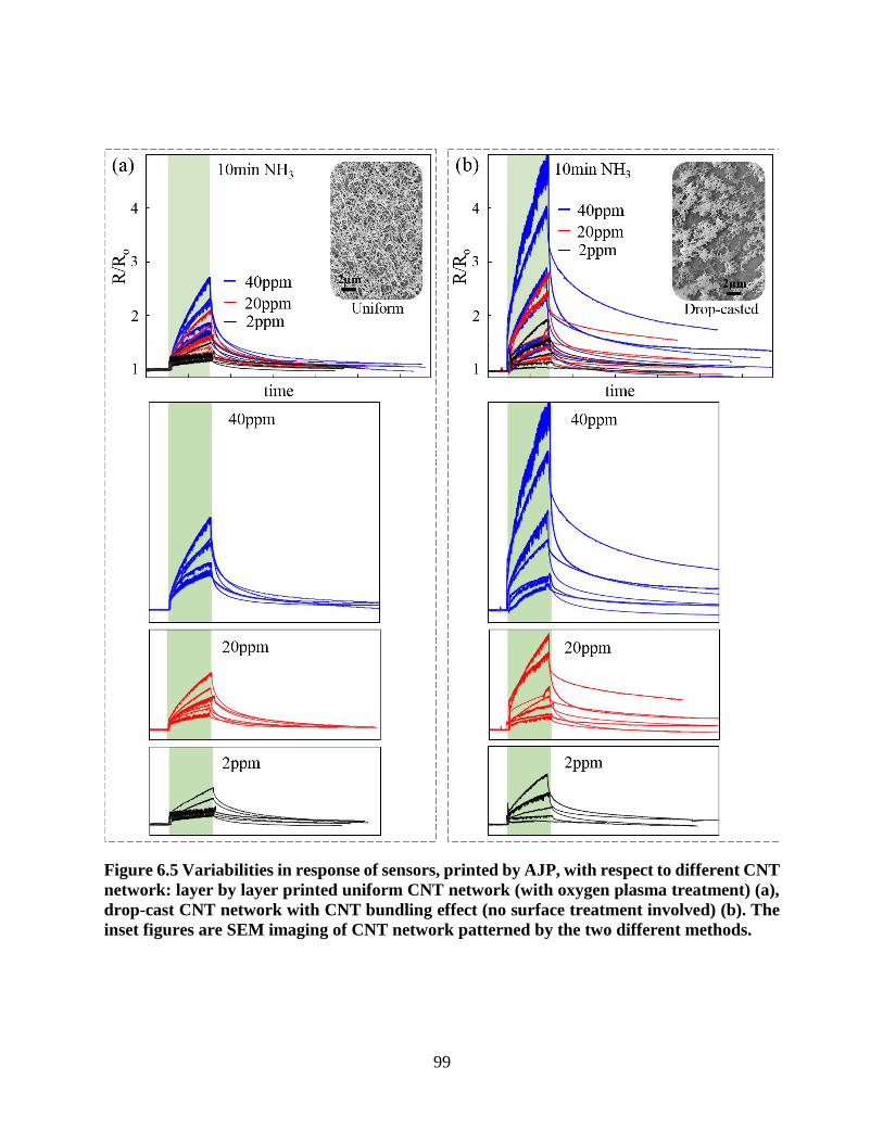
99
Figure 6.5 Variabilities in response of sensors, printed by AJP, with respect to different CNT
network: layer by layer printed uniform CNT network (with oxygen plasma treatment) (a),
drop-cast CNT network with CNT bundling effect (no surface treatment involved) (b). The
inset figures are SEM imaging of CNT network patterned by the two different methods.
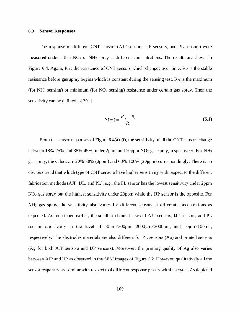
100
6.3 Sensor Responses
The response of different CNT sensors (AJP sensors, IJP sensors, and PL sensors) were
measured under either NO2 or NH3 spray at different concentrations. The results are shown in
Figure 6.4. Again, R is the resistance of CNT sensors which changes over time. Ro is the stable
resistance before gas spray begins which is constant during the sensing test. Rm is the maximum
(for NH3 sensing) or minimum (for NO2 sensing) resistance under certain gas spray. Then the
sensitivity can be defined as[201]
m(%) o
o
R RS
R
−= (6.1)
From the sensor responses of Figure 6.4(a)-(f), the sensitivity of all the CNT sensors change
between 18%-25% and 38%-45% under 2ppm and 20ppm NO2 gas spray, respectively. For NH3
gas spray, the values are 20%-50% (2ppm) and 60%-100% (20ppm) correspondingly. There is no
obvious trend that which type of CNT sensors have higher sensitivity with respect to the different
fabrication methods (AJP, IJL, and PL), e.g., the PL sensor has the lowest sensitivity under 2ppm
NO2 gas spray but the highest sensitivity under 20ppm while the IJP sensor is the opposite. For
NH3 gas spray, the sensitivity also varies for different sensors at different concentrations as
expected. As mentioned earlier, the smallest channel sizes of AJP sensors, IJP sensors, and PL
sensors are nearly in the level of 50μm×500μm, 2000μm×5000μm, and 10μm×100μm,
respectively. The electrodes materials are also different for PL sensors (Au) and printed sensors
(Ag for both AJP sensors and IJP sensors). Moreover, the printing quality of Ag also varies
between AJP and IJP as observed in the SEM images of Figure 6.2. However, qualitatively all the
sensor responses are similar with respect to 4 different response phases within a cycle. As depicted
101
in Figure 6.4(a)-(f), when gas molecules (either NH3 or NO2) reach the surface of the CNT sensors
(gas on state), there is a sudden change in resistance (phase 1) which lasts for only several seconds,
followed by a gradual change in resistance (phase 2) which lasts till gas spray stops (gas off state
begins). As for gas off state, there are also a sudden change (phase 3) and a gradual change (phase
4) in resistance but in the opposite way. Surprisingly, all the sensing curves of individual cycles
can be well characterized by the convolution model described in Chapter 4. Considering all these
distinctions during fabrication, the sensor responses of all the CNT sensors (AJP, IJL, and PL
sensors) do not show very large differences qualitatively. And the printed CNT sensors do not
show conspicuous lower sensitivity compared to PL sensors. The error bars displayed in Figure
6.4(g) reveal the variability of sensitivity of the PL, AJP, and IJP sensors. The average sensitivity
is close to 20% for all the sensors, and the printed sensors even have higher sensitivity. However,
the standard error of the mean shows that the variability of sensitivity changes significantly among
them. For PL sensors, the standard error of the mean is only 2.6% because of much smaller
fabrication difference between individual PL sensors, e.g. more uniformed CNT networks. But for
printed sensors, they are 6.9% (AJP sensors) and 9.3% (IJP sensors).
6.4 Variability of Sensor Responses
The CNTs in the channel are the ultimate gas sensing source, which have significant impact
on the sensitivity. To study the impact of CNT network quality, two types of AJP sensors were
fabricated, i.e., CNT network patterned by two different methods. One is the multiple layer by
layer deposition after treating surface by oxygen plasma (described before in AJP fabrication
section), which ends up with a uniform CNT network. The other one is drop-cast CNT network
without oxygen plasma treatment (mentioned in the IJP fabrication section), which ends up with
severe CNT bundling effect in the network. The rest of fabrication steps are exactly same for these
102
two types of AJP sensors. IJP printed CNT sensors are not utilized here for the comparison because
the yield of printed CNT network is bad using low-cost IJP printers such as Epson C88+ and
Artisan 1430. After fabrication, sensor responses were measured for ~10min NH3 spray at three
different concentrations (2ppm, 20ppm, and 40ppm). The different in results can be observed in
Figure 6.5(a) and 6.5(b), which are under the same coordinates scale. It is quite clear that AJP
sensors with drop-cast CNT network have much larger variability in sensor response than AJP
sensors with uniform CNT network. That is, for all the three different concentrations (2ppm,
20ppm, and 40ppm), the overall resistance change is much larger for AJP sensors with drop-cast
CNT network. Figure 6.6 plots the sensitivity distribution based on the results in Figure 6.5. For
AJP sensors with uniform CNT network (stars), the sensitivity changes in the range of 22%-68%,
38%-105%, and 50%-173% at 2ppm, 20ppm, and 40ppm respectively. But for AJP sensors with
drop-cast CNT network, the corresponding ranges are as large as 10%-99% (2ppm), 25%-182%
(20ppm), and 51%-400% (40ppm).
To explain this significant difference in sensitivity, CNT network is analyzed because the
other processing steps remain same during fabrication. From previous studies, it is known that gas
sensitivity of CNT network based sensors is mainly caused by the CNT/metal contacts and the
CNT junctions[49]. Boyd et al. further pointed out that CNT network effects are dominated by
gas-induced changes at CNT junctions for CNT network based sensors[49]. As shown in the inset
figures of Figure 6.5, the two sets of CNT network are distinct in morphology. That is, the CNT
network in Figure 6.5(a) is highly uniform while severe CNT bundling effect exists almost
everywhere in channel in Figure 6.5(b). Specifically, regional CNT network density, CNT network
structure, CNT-CNT contacts, CNT-metal contacts will vary significantly by the two different
deposition methods. In other words, much higher uncertainty exists for drop-cast CNT network
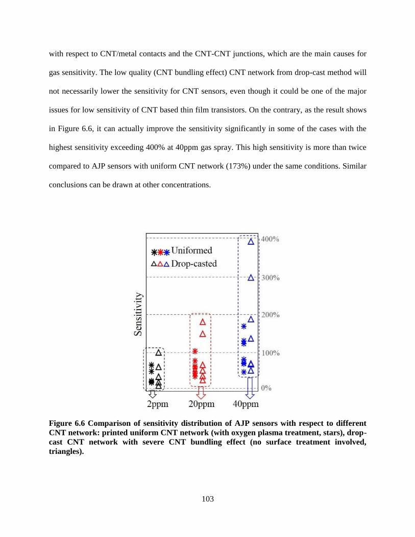
103
with respect to CNT/metal contacts and the CNT-CNT junctions, which are the main causes for
gas sensitivity. The low quality (CNT bundling effect) CNT network from drop-cast method will
not necessarily lower the sensitivity for CNT sensors, even though it could be one of the major
issues for low sensitivity of CNT based thin film transistors. On the contrary, as the result shows
in Figure 6.6, it can actually improve the sensitivity significantly in some of the cases with the
highest sensitivity exceeding 400% at 40ppm gas spray. This high sensitivity is more than twice
compared to AJP sensors with uniform CNT network (173%) under the same conditions. Similar
conclusions can be drawn at other concentrations.
Figure 6.6 Comparison of sensitivity distribution of AJP sensors with respect to different
CNT network: printed uniform CNT network (with oxygen plasma treatment, stars), drop-
cast CNT network with severe CNT bundling effect (no surface treatment involved,
triangles).

104
Figure 6.7 Sensitivity improvement of an IJP sensor under NH3 spray at 2ppm and 20ppm.
Black curve is the sensor response from the original IJP sensor with relatively low sensitivity.
Red curve is the improved sensor response of the IJP sensor with post drop-cast CNT
deposition. The SEM images show the change of CNT network after post drop-cast
deposition.
In some cases, sensitivity could be extremely low for sensors with drop-cast CNT network
because of its high uncertainty compared to uniform CNT network formed by layer by layer
deposition by AJP, e.g., the lowest sensitivity is only 10% for drop-cast CNT network but it is
22% for uniform CNT network at 2ppm concentration, as shown in Figure 6.6. To address this
issue, the unique advantage of drop-cast deposition becomes very beneficial. Unlike uniform CNT
network printed by multiple layer by layer deposition, drop-cast deposition involves no extra
equipment at all and it can be conducted anywhere anytime. Therefore, drop-cast deposition of

105
CNT network can be easily performed after the completion of IJP sensor fabrication (referred as
post drop-cast deposition), in order to improve the low sensitivity of certain IJP sensors. On the
one hand, post drop-cast deposition will neither increase the cost nor complicate the process, which
are the main considerations of the IJP sensors. On the other hand, it can actually rebuild the CNT
network easily and repeatedly to achieve high sensitivity. Figure 6.7 plots the change in sensitivity
before and after the application of post drop-cast CNT network. This improvement is significant.
For the original IJP sensor, the sensitivity is as low as ~6% at 2ppm and ~25% at 20ppm. After
post drop-cast deposition, its sensitivity jumps to ~50% (2ppm) and 150% (20ppm) respectively.
As observed from the SEM images, the CNT network structure is rebuilt (with respect to both local
density and CNT bundling effect) after post drop-cast deposition. This result demonstrates that
post drop-cast deposition can provide an efficient strategy to improve the sensitivity of printed
CNT sensors while maintaining the low-cost, especially for IJP sensors which can be fabricated
outside the cleanroom or even outside the lab because of the simplified steps with cure-free low-
temperature process.
6.5 Closure
Single-walled CNT network based gas sensors have been fabricated using AJP, IJP, and PL
separately. Their sensor responses behave similarly under gas spray of NH3 and NO2 even though
these CNT sensors are different in size, electrodes, and CNT network structure. For fully printed
CNT sensors (either AJP or IJP sensors), no performance degradation has been observed with
respect to sensitivity and stability in response. The significance of CNT network in sensor response
has been demonstrated by comparison of two types AJP sensors with CNT network patterned by
either multiple layer by layer printing (with highly uniform CNT network) or drop-cast method
(with severe CNT bundling effect). Sensors with drop-cast CNT network have much larger

106
variability in sensor response than those with layer by layer printing uniform CNT network.
However, fully printed sensors with very high sensitivity can be fabricated using drop-cast CNT
network. And a post drop-cast deposition can provide an efficient strategy to improve the
sensitivity of printed CNT sensors while maintaining the low-cost nature, which paves the way for
extensive applications of low-cost CNT sensors in flexible and wearable electronics and devices.

107
CHAPTER 7. SUMMARY AND FUTURE WORK
7.1 Summary of Current Work
In this work, randomly distributed CNT network based devices, such as CNT-TFTs and CNT
chemiresistor sensors, have been fabricated on both hard (Si substrate) and flexible substrates
(Kapton, LCP, PET) using PL, AJP, and IJP separately. The performance of CNT-TFTs have been
studied thoroughly and the sensor response of CNT sensors have been improved, which will have
wide range applications in the areas of flexible and wearable electronics, artificial skins, low-cost
CNT sensors, etc.
First, CNT-TFTs on hard Si substrate are fabricated by using PL. To achieve high
performance, >99% highly purified semiconducting single-walled CNT solution is utilized as the
semiconductor material in the channel. However, device-to-device performance variability of
TFTs can pose challenging problems for the fabricated CNT-TFTs. One of the major problems is
the variability in performance, which is mainly rooted in the randomness of CNT networks, the
variation in individual CNT properties due to change in chirality, and the fabrication imperfections.
To address this issue, both experimental and theoretical methods are employed to analyze the
variability in I-V characteristics in a statistical framework. To be specific, the sources of variation
including % of M-CNTs, Vth, CNT mean length, and CNT network density have been studied
separately. The analysis shows that the presence of M-CNTs is a major source contributing to the
performance variation for short channel TFTs, but its effect reduces for large channel length
transistors. Vth is found to be the major source of variation for long channel TFTs. A better
consistency in performance can be guaranteed for TFTs with larger channel area, which ensures a
smaller variation in CNT network density and CNT mean length. These results provide key

108
insights into the variability estimation of I-V characteristics of CNT based devices which is vital
for reliability studies of CNT-TFTs based circuits for different electronic applications.
Secondly, the fabricated CNT-TFTs have been used as sensors for gas detection. It is well
known that the lack of selectivity has been a major drawback of CNT sensors for the wide range
of applications in air quality detection and the industrial emission control. In order to create the
selectivity of CNT sensors with respect to different sensing gases, cycling test of the CNT sensors
have been recorded for NH3 and NO2 detection in air at low ppm concentrations. A sensing
mechanism is proposed based on the interaction between gas molecules and different types of
dwelling spots inside the channel area of a TFT. Moreover, a double exponential-convolution
model is put forward to decipher sensor response as well as to explore its application in gas
identification. In this context, the consistency in time constants is recognized, which is independent
of gas concentration. More importantly, the time constants vary with respect to different gas types
and TFTs. The uniqueness of time constants can work as identity verification for different sensing
gases, which demonstrates that the sensor response is a distinctive behavior determined by the
unique channel structure of each TFT. This work provides us a general strategy for gas
identification and a practical path to realize the advantages of CNT gas sensors in pollution
monitoring in low concentration level.
Then, we concentrate on the fabrication of fully printed CNT-TFTs because of their
significant potential in flexible and wearable devices with huge advantages in the low cost, high
repeatability and scalability. However, quality of printable dielectric layer has become one of the
major obstacles. Its relatively large thickness can result in very high gate voltage to fully switch
on and switch off the transistors, which will cause high power dissipation for printed devices. In
response to this challenge, fully printed CNT-TFTs have been fabricated on Kapton and LCP
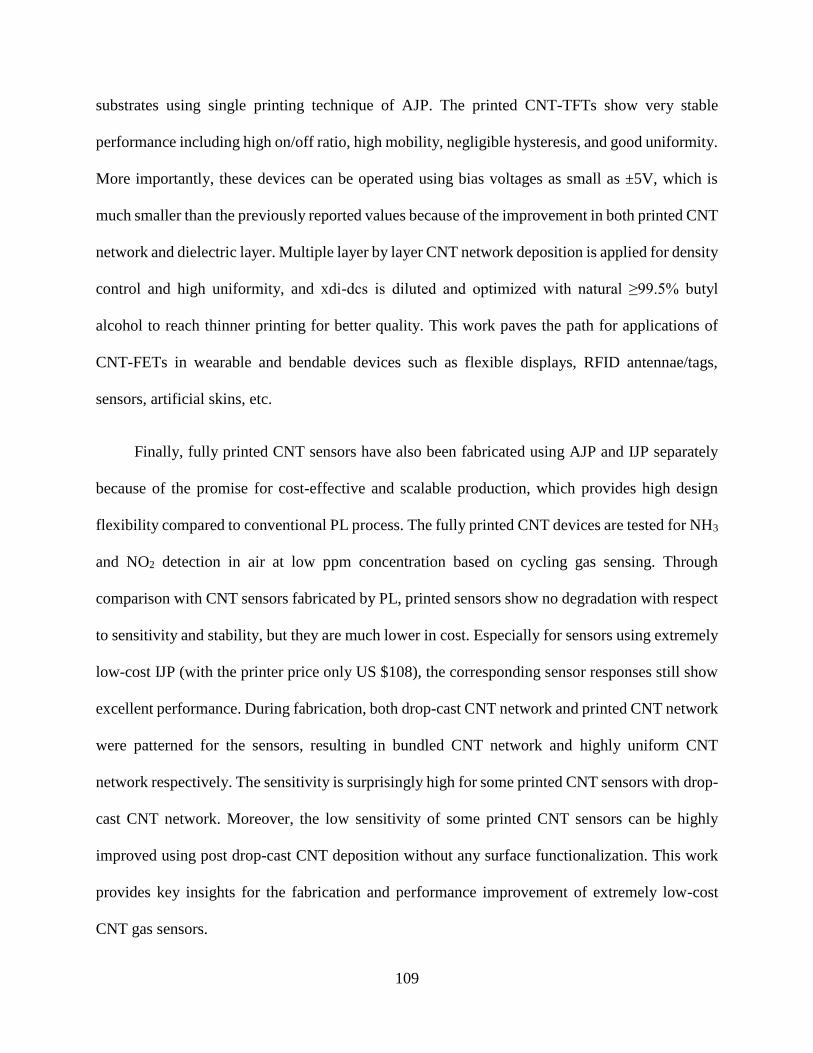
109
substrates using single printing technique of AJP. The printed CNT-TFTs show very stable
performance including high on/off ratio, high mobility, negligible hysteresis, and good uniformity.
More importantly, these devices can be operated using bias voltages as small as ±5V, which is
much smaller than the previously reported values because of the improvement in both printed CNT
network and dielectric layer. Multiple layer by layer CNT network deposition is applied for density
control and high uniformity, and xdi-dcs is diluted and optimized with natural ≥99.5% butyl
alcohol to reach thinner printing for better quality. This work paves the path for applications of
CNT-FETs in wearable and bendable devices such as flexible displays, RFID antennae/tags,
sensors, artificial skins, etc.
Finally, fully printed CNT sensors have also been fabricated using AJP and IJP separately
because of the promise for cost-effective and scalable production, which provides high design
flexibility compared to conventional PL process. The fully printed CNT devices are tested for NH3
and NO2 detection in air at low ppm concentration based on cycling gas sensing. Through
comparison with CNT sensors fabricated by PL, printed sensors show no degradation with respect
to sensitivity and stability, but they are much lower in cost. Especially for sensors using extremely
low-cost IJP (with the printer price only US $108), the corresponding sensor responses still show
excellent performance. During fabrication, both drop-cast CNT network and printed CNT network
were patterned for the sensors, resulting in bundled CNT network and highly uniform CNT
network respectively. The sensitivity is surprisingly high for some printed CNT sensors with drop-
cast CNT network. Moreover, the low sensitivity of some printed CNT sensors can be highly
improved using post drop-cast CNT deposition without any surface functionalization. This work
provides key insights for the fabrication and performance improvement of extremely low-cost
CNT gas sensors.

110
7.2 Future Work
The work in present thesis can be extended and continued in several topics as suggested
below.
7.2.1 Optimization and Improvement of Fully Printed CNT-TFTs
Even though the printed dielectric layer has been highly improved, the overall performance
of fully printed CNT-TFTs are still relatively low considering their high potential. Various aspects
can be further improved and optimized for fully printed CNT-TFTs. The CNT/metal contact is one
of them, which will have significant impact on the overall resistance in printed CNT devices. The
high resistance of CNT/metal contact also can be seen in devices fabricated by PL process, and it
is even worse in printed ones. To address this issue, printed M-CNT layer, as well as graphene
layer, can be a feasible solution. It actually avoids direct CNT/metal contact by introducing
contacts such as S-CNT/M-CNT, M-CNT/metal, S-CNT /graphene, graphene/metal, etc. The
improvement in contact can reduce the performance variability of fully printed CNT-TFTs.
Moreover, the much superior bending and stretching capability of M-CNT layer can also improve
the mechanical performance of printed CNT devices at the same time, e.g., the printed Ag layer
(one-time single printing of AJP) can only survive 20%-30% stretching, but printed CNT layer
(both M-CNT and S-CNT layer) can bear much higher stretching strength (sometimes even higher
than the stretching limit of some flexible substrates such as Kapton with a stretching limit around
60%) because of the excellent mechanical properties of CNTs. Besides, the M-CNTs have the
potential to take the place of printed metal as electrodes of CNT-TFTs, which will have high
potential in transparent electronics. The improvement of fully printed CNT-TFTs can be also be
performed with respect to the dimensions, stability, and reliability of the fabrication process, etc.

111
7.2.2 Mechanical Test of Flexible CNT-TFTs
CNT network based flexible electronics are most commonly used for TFTs as building
blocks for ICs and active-matrix displays, which have great significance in future wearable
devices. The major advantages of flexible CNT-TFTs lie in the excellent mechanical properties
under stress. Generally, there are two types of flexible electronics, stretchable and non-stretchable
(bendable) [202]. Stretchable electronics are usually made of elastomeric substrates such as rubber,
polydimethylsiloxane (PDMS), or polyurethane. Bendable (non-stretchable) electronics usually
use flexible substrates such as thin glass sheets, polyimide, polyethylene terephthalate, or
polyethylene naphthalate. As described earlier, the mechanical test of flexible electronics is of
great significance for various applications. Up to now, most of the researches concentrate on the
bending test of CNT-TFTs. However, flexible CNT-TFTs on non-stretchable substrates can
actually survive from stretching test after improvement during fabrication. This is also very
important for non-stretchable electronics because of the ever-increasing demands in practice. On
the one hand, how the performance changes during stretching test is crucial for the reliability and
stability of the CNT-TFTs. On the other hand, the stretching limit is also the key factor for the
applications of flexible devices. Besides, the mechanical test of flexible CNT-TFTs will give us
feedback on insights about performance improvement of the devices in various ways.
7.2.3 Gas Sensing of Flexible CNT Sensors under Stress
The mechanical test of flexible CNT sensors during gas sensing has attracted more interests
in recent years. As is well-known, gas adsorption in CNTs (including CNT/CNT junctions,
CNT/metal contact, etc.) is an important issue for both fundamental research and technical
application. Both bending test and stretching test need to be performed in order to better understand
112
the sensing mechanism during gas sensing. When gas molecules interact with the CNT network in
channel area, they will work as either electron source or hole source which can either decrease or
increase the current of the sensor depending on the existing current type (either n-type or p-type).
During this process, the CNT/CNT junctions and CNT/metal contact area are the major dwelling
spots for gas molecules. Generally, the dwelling spots stay the same during the gas sensing process.
However, it will be a different situation when CNT sensors are under stress resulting from either
bending or stretching. To be specific, the bending and stretching can change the CNT network
structure more or less because of the deformation in certain area, e.g., the movement of CNTs or
the slide of CNT/CNT junctions in small range. Especially with the increase of stretching strength,
the resistance of the device itself will change significantly because of the change in overall
morphology of the device, which will have significant impact on the sensing performance, such as
the sensitivity, stability, etc.
Figure 7.1 Sensor responses of mixed gases. Same concentration of NH3 at 5ppm (a) and
40ppm (b) with increasing concentration of NO2 for each cycle.

113
7.2.4 Mixed Gas Sensing
Even though it has been proven that CNT sensors are able to detect various gases such as
NH3, NO2, H2, etc., there is very limited work concentrating on the sensing test of mixed gases.
And the corresponding sensor responses have not been fully understood for mixed gas sensing
because of the complicated sensing mechanism. Similarly, cycling tests have has been performed
with gas mixture on for ~10min and gas mixture off for >20min (gas mixture: mix NO2 with NH3
at different concentrations). The results are plotted in Figure 7.1. In Figure 7.1(a), NH3 is
maintained at 5ppm with increasing concentration of NO2 from 5ppm, 20ppm to 40ppm. In Figure
7.1(b), NH3 is maintained at 40ppm with increasing concentration of NO2 from 5ppm to 40ppm.
In both figures, it is observable that all the sensors first experience rapid resistance jump caused
by NH3 for a very short time (dash orange box), then the resistance decreases slowly for the rest
of gas on state caused by NO2 (dash green box). The increasing concentration of NO2 affects the
final resistance at the end of gas on state, while the concentration of NH3 affects the highest
resistance at the beginning of gas on state. Compared to single gas sensing, the sensor responses
of gas mixture are less stable during gas on state. Undoubtedly, further exploration is indispensable
because none of the sensor responses can be well described using any of the previously mentioned
models. Clearly, the sensing mechanism of gas mixture is more complicated than single gas
sensing and it has not been fully understood. More work needs to be done in this area.

114
REFERENCES
[1] R. Martel, T. Schmidt, H. Shea, T. Hertel, and P. Avouris, "Single-and multi-wall carbon
nanotube field-effect transistors," Applied physics letters, vol. 73, no. 17, pp. 2447-2449,
1998.
[2] S. J. Kang et al., "High-performance electronics using dense, perfectly aligned arrays of
single-walled carbon nanotubes," Nature nanotechnology, vol. 2, no. 4, p. 230, 2007.
[3] M. F. De Volder, S. H. Tawfick, R. H. Baughman, and A. J. Hart, "Carbon nanotubes:
present and future commercial applications," science, vol. 339, no. 6119, pp. 535-539,
2013.
[4] H. R. Byon and H. C. Choi, "Network single-walled carbon nanotube-field effect
transistors (SWNT-FETs) with increased Schottky contact area for highly sensitive
biosensor applications," Journal of the American Chemical Society, vol. 128, no. 7, pp.
2188-2189, 2006.
[5] J. C. Johnson, H.-J. Choi, K. P. Knutsen, R. D. Schaller, P. Yang, and R. J. Saykally,
"Single gallium nitride nanowire lasers," Nature materials, vol. 1, no. 2, pp. 106-110, 2002.
[6] Y. Zhang, Y. Bai, and B. Yan, "Functionalized carbon nanotubes for potential medicinal
applications," Drug discovery today, vol. 15, no. 11-12, pp. 428-435, 2010.
[7] P. Chandrasekhar, "CNT Applications in Specialized Materials," in Conducting Polymers,
Fundamentals and Applications: Springer, 2018, pp. 45-48.
[8] P. Avouris, Z. Chen, and V. Perebeinos, "Carbon-based electronics," in Nanoscience And
Technology: A Collection of Reviews from Nature Journals: World Scientific, 2010, pp.
174-184.
[9] C. Qiu, Z. Zhang, M. Xiao, Y. Yang, D. Zhong, and L.-M. Peng, "Scaling carbon nanotube
complementary transistors to 5-nm gate lengths," Science, vol. 355, no. 6322, pp. 271-276,
2017.
[10] Y. Cao et al., "Review of Electronics Based on Single-Walled Carbon Nanotubes," Topics
in Current Chemistry, vol. 375, no. 5, p. 75, 2017.
[11] D. M. Sun, C. Liu, W. C. Ren, and H. M. Cheng, "A Review of Carbon Nanotube‐and
Graphene‐Based Flexible Thin‐Film Transistors," Small, vol. 9, no. 8, pp. 1188-1205,
2013.
[12] D. Fam, A. Palaniappan, A. Tok, B. Liedberg, and S. Moochhala, "A review on
technological aspects influencing commercialization of carbon nanotube sensors," Sensors
and Actuators B: Chemical, vol. 157, no. 1, pp. 1-7, 2011.

115
[13] L.-F. Cui, L. Hu, J. W. Choi, and Y. Cui, "Light-weight free-standing carbon nanotube-
silicon films for anodes of lithium ion batteries," Acs Nano, vol. 4, no. 7, pp. 3671-3678,
2010.
[14] L. Cai and C. Wang, "Carbon nanotube flexible and stretchable electronics," Nanoscale
research letters, vol. 10, no. 1, p. 320, 2015.
[15] S. Nardecchia, D. Carriazo, M. L. Ferrer, M. C. Gutiérrez, and F. del Monte, "Three
dimensional macroporous architectures and aerogels built of carbon nanotubes and/or
graphene: synthesis and applications," Chemical Society Reviews, vol. 42, no. 2, pp. 794-
830, 2013.
[16] X. Li, J. Rong, and B. Wei, "Electrochemical behavior of single-walled carbon nanotube
supercapacitors under compressive stress," Acs Nano, vol. 4, no. 10, pp. 6039-6049, 2010.
[17] A. E. Islam, J. A. Rogers, and M. A. Alam, "Recent Progress in Obtaining Semiconducting
Single‐Walled Carbon Nanotubes for Transistor Applications," Advanced Materials, vol.
27, no. 48, pp. 7908-7937, 2015.
[18] C. De las Casas and W. Li, "A review of application of carbon nanotubes for lithium ion
battery anode material," Journal of Power Sources, vol. 208, pp. 74-85, 2012.
[19] Y. Chen and J. Zhang, "Chemical vapor deposition growth of single-walled carbon
nanotubes with controlled structures for nanodevice applications," Accounts of chemical
research, vol. 47, no. 8, pp. 2273-2281, 2014.
[20] Q. Cao and J. A. Rogers, "Ultrathin films of single‐walled carbon nanotubes for electronics
and sensors: a review of fundamental and applied aspects," Advanced Materials, vol. 21,
no. 1, pp. 29-53, 2009.
[21] C. Wang et al., "Extremely bendable, high-performance integrated circuits using
semiconducting carbon nanotube networks for digital, analog, and radio-frequency
applications," Nano letters, vol. 12, no. 3, pp. 1527-1533, 2012.
[22] Y. Zhao et al., "Three-Dimensional Flexible Complementary Metal–Oxide–
Semiconductor Logic Circuits Based On Two-Layer Stacks of Single-Walled Carbon
Nanotube Networks," ACS nano, vol. 10, no. 2, pp. 2193-2202, 2016.
[23] N. Peng, Q. Zhang, C. L. Chow, O. K. Tan, and N. Marzari, "Sensing mechanisms for
carbon nanotube based NH3 gas detection," Nano letters, vol. 9, no. 4, pp. 1626-1630,
2009.
[24] Y. Wang et al., "Functionalized horizontally aligned CNT array and random CNT network
for CO 2 sensing," Carbon, vol. 117, pp. 263-270, 2017.
[25] T. Zhang, S. Mubeen, N. V. Myung, and M. A. Deshusses, "Recent progress in carbon
nanotube-based gas sensors," Nanotechnology, vol. 19, no. 33, p. 332001, 2008.
116
[26] A. A. Abdelwahab, "Electrochemical Pretreatment of Graphene Composite CNT
Encapsulated Au Nanoparticles for H2O2 Sensor," Electroanalysis, vol. 28, no. 8, pp.
1901-1906, 2016.
[27] B. Sharma, H. Yadav, and J.-S. Kim, "MEMS based hydrogen sensor with the highly
porous Au-CNT film as a sensing material," Journal of Materials Science: Materials in
Electronics, pp. 1-8, 2017.
[28] S. Badhulika, N. V. Myung, and A. Mulchandani, "Conducting polymer coated single-
walled carbon nanotube gas sensors for the detection of volatile organic compounds,"
Talanta, vol. 123, pp. 109-114, 2014.
[29] C. B. Jacobs, M. J. Peairs, and B. J. Venton, "Carbon nanotube based electrochemical
sensors for biomolecules," Analytica chimica acta, vol. 662, no. 2, pp. 105-127, 2010.
[30] M. P. Landry et al., "Single-molecule detection of protein efflux from microorganisms
using fluorescent single-walled carbon nanotube sensor arrays," Nature nanotechnology,
vol. 12, no. 4, p. 368, 2017.
[31] Y. Adiguzel and H. Kulah, "Breath sensors for lung cancer diagnosis," Biosensors and
Bioelectronics, vol. 65, pp. 121-138, 2015.
[32] B. Kim, Y. Lu, T. Kim, J.-W. Han, M. Meyyappan, and J. Li, "Carbon nanotube coated
paper sensor for damage diagnosis," ACS nano, vol. 8, no. 12, pp. 12092-12097, 2014.
[33] F. R. Baptista, S. Belhout, S. Giordani, and S. Quinn, "Recent developments in carbon
nanomaterial sensors," Chemical Society Reviews, vol. 44, no. 13, pp. 4433-4453, 2015.
[34] K. Chen et al., "Printed carbon nanotube electronics and sensor systems," Advanced
Materials, vol. 28, no. 22, pp. 4397-4414, 2016.
[35] B. Chen et al., "Highly uniform carbon nanotube field-effect transistors and medium scale
integrated circuits," Nano letters, vol. 16, no. 8, pp. 5120-5128, 2016.
[36] J. B. Andrews et al., "Patterned Liquid Metal Contacts for Printed Carbon Nanotube
Transistors," ACS nano, 2018.
[37] Q. Cao et al., "Origins and characteristics of the threshold voltage variability of
quasiballistic single-walled carbon nanotube field-effect transistors," ACS nano, vol. 9, no.
2, pp. 1936-1944, 2015.
[38] Q. Cao, J. Tersoff, S.-J. Han, and A. V. Penumatcha, "Scaling of device variability and
subthreshold swing in ballistic carbon nanotube transistors," Physical Review Applied, vol.
4, no. 2, p. 024022, 2015.
[39] C. G. Almudéver and A. Rubio, "Variability and reliability analysis of CNFET in the
presence of carbon nanotube density fluctuations," in Mixed Design of Integrated Circuits

117
and Systems (MIXDES), 2012 Proceedings of the 19th International Conference, 2012, pp.
124-129: IEEE.
[40] A. E. Islam, F. Du, X. Ho, S. Hun Jin, S. Dunham, and J. A. Rogers, "Effect of variations
in diameter and density on the statistics of aligned array carbon-nanotube field effect
transistors," Journal of Applied Physics, vol. 111, no. 5, p. 054511, 2012.
[41] A. D. Franklin et al., "Variability in carbon nanotube transistors: Improving device-to-
device consistency," ACS nano, vol. 6, no. 2, pp. 1109-1115, 2012.
[42] N.-P. Wang, S. Heinze, and J. Tersoff, "Random-telegraph-signal noise and device
variability in ballistic nanotube transistors," Nano letters, vol. 7, no. 4, pp. 910-913, 2007.
[43] J. Kong et al., "Nanotube molecular wires as chemical sensors," science, vol. 287, no. 5453,
pp. 622-625, 2000.
[44] J. Zhao, A. Buldum, J. Han, and J. P. Lu, "Gas molecule adsorption in carbon nanotubes
and nanotube bundles," Nanotechnology, vol. 13, no. 2, p. 195, 2002.
[45] T. Someya, J. Small, P. Kim, C. Nuckolls, and J. T. Yardley, "Alcohol vapor sensors based
on single-walled carbon nanotube field effect transistors," Nano letters, vol. 3, no. 7, pp.
877-881, 2003.
[46] K. Bradley, J.-C. P. Gabriel, M. Briman, A. Star, and G. Grüner, "Charge transfer from
ammonia physisorbed on nanotubes," Physical review letters, vol. 91, no. 21, p. 218301,
2003.
[47] H. Chang, J. D. Lee, S. M. Lee, and Y. H. Lee, "Adsorption of NH 3 and NO 2 molecules
on carbon nanotubes," Applied Physics Letters, vol. 79, no. 23, pp. 3863-3865, 2001.
[48] Y. Battie et al., "Gas sensors based on thick films of semi-conducting single walled carbon
nanotubes," Carbon, vol. 49, no. 11, pp. 3544-3552, 2011.
[49] A. Boyd, I. Dube, G. Fedorov, M. Paranjape, and P. Barbara, "Gas sensing mechanism of
carbon nanotubes: from single tubes to high-density networks," Carbon, vol. 69, pp. 417-
423, 2014.
[50] F. Rigoni et al., "Enhancing the sensitivity of chemiresistor gas sensors based on pristine
carbon nanotubes to detect low-ppb ammonia concentrations in the environment," Analyst,
vol. 138, no. 24, pp. 7392-7399, 2013.
[51] L. Cai et al., "Direct printing for additive patterning of silver nanowires for stretchable
sensor and display applications," Advanced Materials Technologies, vol. 3, no. 2, p.
1700232, 2018.
[52] J. Zhang, G. Y. Tian, A. M. Marindra, A. I. Sunny, and A. B. Zhao, "A review of passive
RFID tag antenna-based sensors and systems for structural health monitoring applications,"
Sensors, vol. 17, no. 2, p. 265, 2017.
118
[53] R. Singh, E. Singh, and H. S. Nalwa, "Inkjet printed nanomaterial based flexible radio
frequency identification (RFID) tag sensors for the internet of nano things," RSC Advances,
vol. 7, no. 77, pp. 48597-48630, 2017.
[54] M. Bariya et al., "Roll-to-Roll Gravure Printed Electrochemical Sensors for Wearable and
Medical Devices," ACS nano, 2018.
[55] M. Amjadi, K. U. Kyung, I. Park, and M. Sitti, "Stretchable, skin‐mountable, and wearable
strain sensors and their potential applications: a review," Advanced Functional Materials,
vol. 26, no. 11, pp. 1678-1698, 2016.
[56] S. Harada, K. Kanao, Y. Yamamoto, T. Arie, S. Akita, and K. Takei, "Fully printed flexible
fingerprint-like three-axis tactile and slip force and temperature sensors for artificial skin,"
ACS nano, vol. 8, no. 12, pp. 12851-12857, 2014.
[57] I.-C. Cheng, "Flexible and Printed Electronics," in Materials for Advanced Packaging:
Springer, 2017, pp. 813-854.
[58] M. Ha et al., "Aerosol jet printed, low voltage, electrolyte gated carbon nanotube ring
oscillators with sub-5 μs stage delays," Nano letters, vol. 13, no. 3, pp. 954-960, 2013.
[59] A. Mahajan, C. D. Frisbie, and L. F. Francis, "Optimization of aerosol jet printing for high-
resolution, high-aspect ratio silver lines," ACS applied materials & interfaces, vol. 5, no.
11, pp. 4856-4864, 2013.
[60] P. M. Grubb, H. Subbaraman, S. Park, D. Akinwande, and R. T. Chen, "Inkjet printing of
high performance transistors with micron order chemically set gaps," Scientific reports,
vol. 7, no. 1, p. 1202, 2017.
[61] C. Cao, J. B. Andrews, A. Kumar, and A. D. Franklin, "Improving contact interfaces in
fully printed carbon nanotube thin-film transistors," ACS nano, vol. 10, no. 5, pp. 5221-
5229, 2016.
[62] Y. Che, H. Chen, H. Gui, J. Liu, B. Liu, and C. Zhou, "Review of carbon nanotube
nanoelectronics and macroelectronics," Semiconductor Science and Technology, vol. 29,
no. 7, p. 073001, 2014.
[63] K. R. Zope, D. Cormier, and S. A. Williams, "Reactive Silver Oxalate Ink Composition
with Enhanced Curing Conditions for Flexible Substrates," ACS applied materials &
interfaces, vol. 10, no. 4, pp. 3830-3837, 2018.
[64] J. Lefebvre, J. Ding, Z. Li, P. Finnie, G. Lopinski, and P. R. Malenfant, "High-purity
semiconducting single-walled carbon nanotubes: a key enabling material in emerging
electronics," Accounts of chemical research, vol. 50, no. 10, pp. 2479-2486, 2017.
[65] M. Ha et al., "Printed, sub-3V digital circuits on plastic from aqueous carbon nanotube
inks," ACS nano, vol. 4, no. 8, pp. 4388-4395, 2010.
119
[66] K. Hong et al., "Aerosol Jet Printed, Sub‐2 V Complementary Circuits Constructed from
P‐and N‐Type Electrolyte Gated Transistors," Advanced Materials, vol. 26, no. 41, pp.
7032-7037, 2014.
[67] L. Cai, S. Zhang, J. Miao, Z. Yu, and C. Wang, "Fully printed stretchable thin-film
transistors and integrated logic circuits," ACS nano, vol. 10, no. 12, pp. 11459-11468, 2016.
[68] C. Cao, J. B. Andrews, and A. D. Franklin, "Completely Printed, Flexible, Stable, and
Hysteresis‐Free Carbon Nanotube Thin‐Film Transistors via Aerosol Jet Printing,"
Advanced Electronic Materials, vol. 3, no. 5, p. 1700057, 2017.
[69] K. Hong, S. H. Kim, A. Mahajan, and C. D. Frisbie, "Aerosol Jet Printed p-and n-type
Electrolyte-Gated Transistors with a Variety of Electrode Materials: Exploring Practical
Routes to Printed Electronics," ACS applied materials & interfaces, vol. 6, no. 21, pp.
18704-18711, 2014.
[70] R. Saito, G. Dresselhaus, and M. S. Dresselhaus, Physical properties of carbon nanotubes.
World Scientific, 1998.
[71] T. Dürkop, S. Getty, E. Cobas, and M. Fuhrer, "Extraordinary mobility in semiconducting
carbon nanotubes," Nano letters, vol. 4, no. 1, pp. 35-39, 2004.
[72] X. Zhou, J.-Y. Park, S. Huang, J. Liu, and P. L. McEuen, "Band structure, phonon
scattering, and the performance limit of single-walled carbon nanotube transistors,"
Physical Review Letters, vol. 95, no. 14, p. 146805, 2005.
[73] L. Hu, D. S. Hecht, and G. Gruner, "Carbon nanotube thin films: fabrication, properties,
and applications," Chemical reviews, vol. 110, no. 10, pp. 5790-5844, 2010.
[74] B. Yakobson, M. Campbell, C. Brabec, and J. Bernholc, "High strain rate fracture and C-
chain unraveling in carbon nanotubes," Computational Materials Science, vol. 8, no. 4, pp.
341-348, 1997.
[75] R. S. Ruoff and D. C. Lorents, "Mechanical and thermal properties of carbon nanotubes,"
carbon, vol. 33, no. 7, pp. 925-930, 1995.
[76] T. W. Tombler et al., "Reversible electromechanical characteristics of carbon nanotubes
under local-probe manipulation," Nature, vol. 405, no. 6788, pp. 769-772, 2000.
[77] B.-H. Chen et al., "Complementary carbon nanotube-gated carbon nanotube thin-film
transistor," Applied physics letters, vol. 88, no. 9, p. 093502, 2006.
[78] O. Matarredona, H. Rhoads, Z. Li, J. H. Harwell, L. Balzano, and D. E. Resasco,
"Dispersion of single-walled carbon nanotubes in aqueous solutions of the anionic
surfactant NaDDBS," The Journal of Physical Chemistry B, vol. 107, no. 48, pp. 13357-
13367, 2003.

120
[79] M. Seo et al., "Terahertz electromagnetic interference shielding using single-walled carbon
nanotube flexible films," Applied Physics Letters, vol. 93, no. 23, p. 231905, 2008.
[80] C. Wang, K. Takei, T. Takahashi, and A. Javey, "Carbon nanotube electronics–moving
forward," Chemical Society Reviews, vol. 42, no. 7, pp. 2592-2609, 2013.
[81] Y. Wang, S. K. R. Pillai, and M. B. Chan‐Park, "High‐Performance Partially Aligned
Semiconductive Single‐Walled Carbon Nanotube Transistors Achieved with a Parallel
Technique," Small, vol. 9, no. 17, pp. 2960-2969, 2013.
[82] G. Li et al., "Fabrication of air-stable n-type carbon nanotube thin-film transistors on
flexible substrates using bilayer dielectrics," Nanoscale, vol. 7, no. 42, pp. 17693-17701,
2015.
[83] M. L. Geier et al., "Solution-processed carbon nanotube thin-film complementary static
random access memory," Nature nanotechnology, vol. 10, no. 11, p. 944, 2015.
[84] M. L. Geier et al., "Subnanowatt carbon nanotube complementary logic enabled by
threshold voltage control," Nano letters, vol. 13, no. 10, pp. 4810-4814, 2013.
[85] P. Feng et al., "Printed Neuromorphic Devices Based on Printed Carbon Nanotube Thin‐Film Transistors," Advanced Functional Materials, vol. 27, no. 5, p. 1604447, 2017.
[86] M. Muoth, T. Helbling, L. Durrer, S.-W. Lee, C. Roman, and C. Hierold, "Hysteresis-free
operation of suspended carbon nanotube transistors," Nature Nanotechnology, vol. 5, no.
8, p. 589, 2010.
[87] J. S. Lee, S. Ryu, K. Yoo, I. S. Choi, W. S. Yun, and J. Kim, "Origin of gate hysteresis in
carbon nanotube field-effect transistors," The Journal of Physical Chemistry C, vol. 111,
no. 34, pp. 12504-12507, 2007.
[88] H. G. Ong et al., "Origin of hysteresis in the transfer characteristic of carbon nanotube field
effect transistor," Journal of Physics D: Applied Physics, vol. 44, no. 28, p. 285301, 2011.
[89] W. Kim, A. Javey, O. Vermesh, Q. Wang, Y. Li, and H. Dai, "Hysteresis caused by water
molecules in carbon nanotube field-effect transistors," Nano Letters, vol. 3, no. 2, pp. 193-
198, 2003.
[90] S. H. Jin, A. E. Islam, T. i. Kim, J. h. Kim, M. A. Alam, and J. A. Rogers, "Sources of
Hysteresis in Carbon Nanotube Field‐Effect Transistors and Their Elimination Via
Methylsiloxane Encapsulants and Optimized Growth Procedures," Advanced Functional
Materials, vol. 22, no. 11, pp. 2276-2284, 2012.
[91] W. J. Yu et al., "Small hysteresis nanocarbon-based integrated circuits on flexible and
transparent plastic substrate," Nano letters, vol. 11, no. 3, pp. 1344-1350, 2011.
121
[92] T.-J. Ha, D. Kiriya, K. Chen, and A. Javey, "Highly stable hysteresis-free carbon nanotube
thin-film transistors by fluorocarbon polymer encapsulation," ACS applied materials &
interfaces, vol. 6, no. 11, pp. 8441-8446, 2014.
[93] J. Tittmann et al., "Hysteresis-free carbon nanotube field-effect transistors without
passivation," in Proceedings of the 2014 IEEE/ACM International Symposium on
Nanoscale Architectures, 2014, pp. 137-138: ACM.
[94] M. Shlafman, T. Tabachnik, O. Shtempluk, A. Razin, V. Kochetkov, and Y. Yaish, "Self
aligned hysteresis free carbon nanotube field-effect transistors," Applied Physics Letters,
vol. 108, no. 16, p. 163104, 2016.
[95] R. S. Park, G. Hills, J. Sohn, S. Mitra, M. M. Shulaker, and H.-S. P. Wong, "Hysteresis-
free carbon nanotube field-effect transistors," ACS nano, vol. 11, no. 5, pp. 4785-4791,
2017.
[96] M. Muoth and C. Hierold, "Transfer of carbon nanotubes onto microactuators for
hysteresis-free transistors at low thermal budget," in Micro Electro Mechanical Systems
(MEMS), 2012 IEEE 25th International Conference on, 2012, pp. 1352-1355: IEEE.
[97] S. A. McGill, S. G. Rao, P. Manandhar, P. Xiong, and S. Hong, "High-performance,
hysteresis-free carbon nanotube field-effect transistors via directed assembly," Applied
physics letters, vol. 89, no. 16, p. 163123, 2006.
[98] J. Cao, S. T. Bartsch, and A. M. Ionescu, "Wafer-level hysteresis-free resonant carbon
nanotube transistors," ACS nano, vol. 9, no. 3, pp. 2836-2842, 2015.
[99] S. Borkar, "Designing reliable systems from unreliable components: the challenges of
transistor variability and degradation," Ieee Micro, vol. 25, no. 6, pp. 10-16, 2005.
[100] A. E. Islam, "Variability and reliability of single-walled carbon nanotube field effect
transistors," Electronics, vol. 2, no. 4, pp. 332-367, 2013.
[101] S. Salamat, X. Ho, J. A. Rogers, and M. A. Alam, "Intrinsic performance variability in
aligned array CNFETs," IEEE Transactions on Nanotechnology, vol. 10, no. 3, pp. 439-
444, 2011.
[102] Z. Hu, G. S. Tulevski, J. B. Hannon, A. Afzali, M. Liehr, and H. Park, "Variability and
reliability analysis in self-assembled multichannel carbon nanotube field-effect
transistors," Applied Physics Letters, vol. 106, no. 24, p. 243106, 2015.
[103] C. G. Almudever and A. Rubio, "Variability and reliability analysis of CNFET technology:
Impact of manufacturing imperfections," Microelectronics Reliability, vol. 55, no. 2, pp.
358-366, 2015.
[104] A. Martinez, M. Aldegunde, N. Seoane, A. R. Brown, J. R. Barker, and A. Asenov,
"Quantum-transport study on the impact of channel length and cross sections on variability

122
induced by random discrete dopants in narrow gate-all-around silicon nanowire
transistors," IEEE Transactions on Electron Devices, vol. 58, no. 8, pp. 2209-2217, 2011.
[105] A. Asenov et al., "Advanced simulation of statistical variability and reliability in nano
CMOS transistors," in Electron Devices Meeting, 2008. IEDM 2008. IEEE International,
2008, pp. 1-1: IEEE.
[106] A. D. Franklin, D. B. Farmer, and W. Haensch, "Defining and overcoming the contact
resistance challenge in scaled carbon nanotube transistors," ACS nano, vol. 8, no. 7, pp.
7333-7339, 2014.
[107] D. Shahrjerdi, A. D. Franklin, S. Oida, J. A. Ott, G. S. Tulevski, and W. Haensch, "High-
performance air-stable n-type carbon nanotube transistors with erbium contacts," ACS
nano, vol. 7, no. 9, pp. 8303-8308, 2013.
[108] Y. Chai et al., "Low-resistance electrical contact to carbon nanotubes with graphitic
interfacial layer," IEEE Transactions on Electron Devices, vol. 59, no. 1, pp. 12-19, 2012.
[109] Q. Cao, S.-J. Han, G. S. Tulevski, A. D. Franklin, and W. Haensch, "Evaluation of field-
effect mobility and contact resistance of transistors that use solution-processed single-
walled carbon nanotubes," ACS nano, vol. 6, no. 7, pp. 6471-6477, 2012.
[110] S. Wang et al., "High-performance carbon nanotube light-emitting diodes with asymmetric
contacts," Nano letters, vol. 11, no. 1, pp. 23-29, 2010.
[111] C. Wang, K. Ryu, A. Badmaev, J. Zhang, and C. Zhou, "Metal contact engineering and
registration-free fabrication of complementary metal-oxide semiconductor integrated
circuits using aligned carbon nanotubes," Acs Nano, vol. 5, no. 2, pp. 1147-1153, 2011.
[112] Y.-C. Tseng and J. Bokor, "Characterization of the junction capacitance of metal-
semiconductor carbon nanotube Schottky contacts," Applied Physics Letters, vol. 96, no.
1, p. 013103, 2010.
[113] J. Svensson and E. E. Campbell, "Schottky barriers in carbon nanotube-metal contacts,"
Journal of applied physics, vol. 110, no. 11, p. 16, 2011.
[114] P. M. Solomon, "Contact resistance to a one-dimensional quasi-ballistic nanotube/wire,"
IEEE Electron Device Letters, vol. 32, no. 3, pp. 246-248, 2011.
[115] D. J. Perello et al., "Anomalous schottky barriers and contact band-to-band tunneling in
carbon nanotube transistors," ACS nano, vol. 4, no. 6, pp. 3103-3108, 2010.
[116] S. H. Kim et al., "Carbon nanotube and graphene hybrid thin film for transparent electrodes
and field effect transistors," Advanced Materials, vol. 26, no. 25, pp. 4247-4252, 2014.
[117] M. L. Geier, K. Moudgil, S. Barlow, S. R. Marder, and M. C. Hersam, "Controlled n-type
doping of carbon nanotube transistors by an organorhodium dimer," Nano letters, vol. 16,
no. 7, pp. 4329-4334, 2016.
123
[118] T.-J. Ha, K. Chen, S. Chuang, K. M. Yu, D. Kiriya, and A. Javey, "Highly uniform and
stable n-type carbon nanotube transistors by using positively charged silicon nitride thin
films," Nano letters, vol. 15, no. 1, pp. 392-397, 2014.
[119] J.-Y. Jeon and T.-J. Ha, "High-Performance Single-Walled Carbon Nanotube-Based Thin-
Film Transistors by Reducing Charge Transfer," IEEE Transactions on Electron Devices,
vol. 63, no. 2, pp. 827-831, 2016.
[120] S.-J. Choi, P. Bennett, D. Lee, and J. Bokor, "Highly uniform carbon nanotube nanomesh
network transistors," Nano Research, vol. 8, no. 4, pp. 1320-1326, 2015.
[121] B. Li, L. Wang, and G. Casati, "Negative differential thermal resistance and thermal
transistor," Applied Physics Letters, vol. 88, no. 14, p. 143501, 2006.
[122] M. E. Itkis, F. Borondics, A. Yu, and R. C. Haddon, "Thermal conductivity measurements
of semitransparent single-walled carbon nanotube films by a bolometric technique," Nano
letters, vol. 7, no. 4, pp. 900-904, 2007.
[123] J. Lee, A. Liao, E. Pop, and W. P. King, "Electrical and thermal coupling to a single-wall
carbon nanotube device using an electrothermal nanoprobe," Nano letters, vol. 9, no. 4, pp.
1356-1361, 2009.
[124] S. Park, M. Vosguerichian, and Z. Bao, "A review of fabrication and applications of carbon
nanotube film-based flexible electronics," Nanoscale, vol. 5, no. 5, pp. 1727-1752, 2013.
[125] B. Kim, S. Jang, M. L. Geier, P. L. Prabhumirashi, M. C. Hersam, and A. Dodabalapur,
"High-speed, inkjet-printed carbon nanotube/zinc tin oxide hybrid complementary ring
oscillators," Nano letters, vol. 14, no. 6, pp. 3683-3687, 2014.
[126] C. M. Homenick et al., "Fully printed and encapsulated SWCNT-based thin film transistors
via a combination of R2R gravure and inkjet printing," ACS applied materials & interfaces,
vol. 8, no. 41, pp. 27900-27910, 2016.
[127] B. Kim, M. L. Geier, M. C. Hersam, and A. Dodabalapur, "Inkjet printed circuits based on
ambipolar and p-type carbon nanotube thin-film transistors," Scientific Reports, vol. 7, p.
39627, 2017.
[128] J. Vaillancourt et al., "All ink-jet-printed carbon nanotube thin-film transistor on a
polyimide substrate with an ultrahigh operating frequency of over 5 GHz," Applied Physics
Letters, vol. 93, no. 24, p. 444, 2008.
[129] P. M. Grubb, H. Subbaraman, S. Park, D. Akinwande, and R. T. Chen, "Inkjet Printing of
High Performance Transistors with Micron Order Chemically Set Gaps," Scientific
Reports, vol. 7, 2017.
[130] X. Cao, F. Wu, C. Lau, Y. Liu, Q. Liu, and C. Zhou, "Top-Contact Self-Aligned Printing
for High-Performance Carbon Nanotube Thin-Film Transistors with Sub-Micron Channel
Length," ACS nano, vol. 11, no. 2, pp. 2008-2014, 2017.
124
[131] S. K. Eshkalak, A. Chinnappan, W. Jayathilaka, M. Khatibzadeh, E. Kowsari, and S.
Ramakrishna, "A review on inkjet printing of CNT composites for smart applications,"
Applied Materials Today, vol. 9, pp. 372-386, 2017.
[132] P. Chandrasekhar, "Miscellaneous CNT Applications," in Conducting Polymers,
Fundamentals and Applications: Springer, 2018, pp. 89-90.
[133] P. Chandrasekhar, "CNT Applications in Displays and Transparent, Conductive
Films/Substrates," in Conducting Polymers, Fundamentals and Applications: Springer,
2018, pp. 73-75.
[134] M. A. Monne, E. Enuka, Z. Wang, and M. Y. Chen, "Inkjet printed graphene-based field-
effect transistors on flexible substrate," in Low-Dimensional Materials and Devices 2017,
2017, vol. 10349, p. 1034905: International Society for Optics and Photonics.
[135] Y. Li et al., "All inkjet-printed metal-oxide thin-film transistor array with good stability
and uniformity using surface-energy patterns," ACS applied materials & interfaces, vol. 9,
no. 9, pp. 8194-8200, 2017.
[136] Y. Lee et al., "Semiconducting carbon nanotube network thin-film transistors with
enhanced inkjet-printed source and drain contact interfaces," Applied Physics Letters, vol.
111, no. 17, p. 173108, 2017.
[137] B. Kim, S. Jang, M. L. Geier, P. L. Prabhumirashi, M. C. Hersam, and A. Dodabalapur,
"Inkjet printed ambipolar transistors and inverters based on carbon nanotube/zinc tin oxide
heterostructures," Applied Physics Letters, vol. 104, no. 6, p. 062101, 2014.
[138] S. Jang, S. Kim, M. L. Geier, M. C. Hersam, and A. Dodabalapur, "Inkjet printed carbon
nanotubes in short channel field effect transistors: influence of nanotube distortion and gate
insulator interface modification," Flexible and Printed Electronics, vol. 1, no. 3, p. 035001,
2016.
[139] S. Horike et al., "Thermodynamics and kinetics of polyoxyethylene alkyl ether evaporation
from inkjet-printed carbon nanotube thin films by vacuum annealing," Flexible and Printed
Electronics, vol. 3, no. 2, p. 025006, 2018.
[140] S. G. Bucella et al., "Inkjet Printed Single‐Walled Carbon Nanotube Based Ambipolar and
Unipolar Transistors for High‐Performance Complementary Logic Circuits," Advanced
Electronic Materials, vol. 2, no. 6, p. 1600094, 2016.
[141] T. Seifert, E. Sowade, F. Roscher, M. Wiemer, T. Gessner, and R. R. Baumann, "Additive
manufacturing technologies compared: morphology of deposits of silver ink using inkjet
and aerosol jet printing," Industrial & Engineering Chemistry Research, vol. 54, no. 2, pp.
769-779, 2015.
[142] J. A. Paulsen, M. Renn, K. Christenson, and R. Plourde, "Printing conformal electronics
on 3D structures with Aerosol Jet technology," in Future of Instrumentation International
Workshop (FIIW), 2012, 2012, pp. 1-4: IEEE.
125
[143] A. Mette, P. Richter, M. Hörteis, and S. Glunz, "Metal aerosol jet printing for solar cell
metallization," Progress in Photovoltaics: Research and Applications, vol. 15, no. 7, pp.
621-627, 2007.
[144] B. King and M. Renn, "Aerosol Jet direct write printing for mil-aero electronic
applications," in Lockheed Martin Palo Alto Colloquia, Palo Alto, CA, 2009.
[145] M. Held et al., "Dense Carbon Nanotube Films as Transparent Electrodes in Low‐Voltage
Polymer and All‐Carbon Transistors," Advanced Electronic Materials, p. 1700331, 2017.
[146] J. B. Andrews, J. A. Cardenas, C. J. Lim, S. G. Noyce, J. Mullett, and A. D. Franklin,
"Fully Printed and Flexible Carbon Nanotube Transistors for Pressure Sensing In
Automobile Tires," IEEE Sensors Journal, 2018.
[147] M. Rother et al., "Aerosol‐Jet Printing of Polymer‐Sorted (6, 5) Carbon Nanotubes for
Field‐Effect Transistors with High Reproducibility," Advanced Electronic Materials, vol.
3, no. 8, p. 1700080, 2017.
[148] J. A. Cardenas, M. J. Catenacci, J. B. Andrews, N. X. Williams, B. J. Wiley, and A. D.
Franklin, "In-Place Printing of Carbon Nanotube Transistors at Low Temperature," ACS
Applied Nano Materials, vol. 1, no. 4, pp. 1863-1869, 2018.
[149] J. Zhao, Y. Gao, J. Lin, Z. Chen, and Z. Cui, "Printed thin-film transistors with
functionalized single-walled carbon nanotube inks," Journal of Materials Chemistry, vol.
22, no. 5, pp. 2051-2056, 2012.
[150] D. Song, F. Zare Bidoky, W. J. Hyun, S. B. Walker, J. A. Lewis, and C. D. Frisbie, "All-
Printed, Self-Aligned Carbon Nanotube Thin-Film Transistors on Imprinted Plastic
Substrates," ACS applied materials & interfaces, vol. 10, no. 18, pp. 15926-15932, 2018.
[151] C. S. Jones, X. Lu, M. Renn, M. Stroder, and W.-S. Shih, "Aerosol-jet-printed, high-speed,
flexible thin-film transistor made using single-walled carbon nanotube solution,"
Microelectronic Engineering, vol. 87, no. 3, pp. 434-437, 2010.
[152] J. H. Cho et al., "Printable ion-gel gate dielectrics for low-voltage polymer thin-film
transistors on plastic," Nature materials, vol. 7, no. 11, p. 900, 2008.
[153] D. H. Craston, C. P. Jones, D. E. Williams, and N. El Murr, "Microband electrodes
fabricated by screen printing processes: applications in electroanalysis," Talanta, vol. 38,
no. 1, pp. 17-26, 1991.
[154] K. Jost et al., "Knitted and screen printed carbon-fiber supercapacitors for applications in
wearable electronics," Energy & Environmental Science, vol. 6, no. 9, pp. 2698-2705,
2013.
[155] T. Blumenthal et al., "Patterned direct-write and screen-printing of NIR-to-visible
upconverting inks for security applications," Nanotechnology, vol. 23, no. 18, p. 185305,
2012.
126
[156] X. Cao et al., "Screen printing as a scalable and low-cost approach for rigid and flexible
thin-film transistors using separated carbon nanotubes," ACS nano, vol. 8, no. 12, pp.
12769-12776, 2014.
[157] X. Cao et al., "Fully screen-printed, large-area, and flexible active-matrix electrochromic
displays using carbon nanotube thin-film transistors," ACS nano, vol. 10, no. 11, pp. 9816-
9822, 2016.
[158] A. J. Bandodkar, I. Jeerapan, J.-M. You, R. Nunez-Flores, and J. Wang, "Highly stretchable
fully-printed CNT-based electrochemical sensors and biofuel cells: Combining intrinsic
and design-induced stretchability," Nano letters, vol. 16, no. 1, pp. 721-727, 2015.
[159] J. Noh et al., "Scalability of roll-to-roll gravure-printed electrodes on plastic foils," IEEE
Transactions on Electronics Packaging Manufacturing, vol. 33, no. 4, pp. 275-283, 2010.
[160] W. Lee et al., "A fully roll-to-roll gravure-printed carbon nanotube-based active matrix for
multi-touch sensors," Scientific reports, vol. 5, p. 17707, 2015.
[161] H. Koo et al., "Scalability of carbon-nanotube-based thin film transistors for flexible
electronic devices manufactured using an all roll-to-roll gravure printing system,"
Scientific reports, vol. 5, p. 14459, 2015.
[162] J. Noh et al., "Fully gravure-printed D flip-flop on plastic foils using single-walled carbon-
nanotube-based TFTs," IEEE Electron Device Letters, vol. 32, no. 5, pp. 638-640, 2011.
[163] Q. Cao et al., "Medium-scale carbon nanotube thin-film integrated circuits on flexible
plastic substrates," Nature, vol. 454, no. 7203, p. 495, 2008.
[164] D.-m. Sun et al., "Flexible high-performance carbon nanotube integrated circuits," Nature
nanotechnology, vol. 6, no. 3, p. 156, 2011.
[165] H. Wang et al., "Tuning the threshold voltage of carbon nanotube transistors by n-type
molecular doping for robust and flexible complementary circuits," Proceedings of the
National Academy of Sciences, p. 201320045, 2014.
[166] B. W. Wang et al., "Continuous Fabrication of Meter‐Scale Single‐Wall Carbon Nanotube
Films and their Use in Flexible and Transparent Integrated Circuits," Advanced Materials,
vol. 30, no. 32, p. 1802057, 2018.
[167] J. Zhang, C. Wang, and C. Zhou, "Rigid/flexible transparent electronics based on separated
carbon nanotube thin-film transistors and their application in display electronics," Acs
Nano, vol. 6, no. 8, pp. 7412-7419, 2012.
[168] A. Schindler, J. Brill, N. Fruehauf, J. P. Novak, and Z. Yaniv, "Solution-deposited carbon
nanotube layers for flexible display applications," Physica E: Low-Dimensional Systems
and Nanostructures, vol. 37, no. 1-2, pp. 119-123, 2007.

127
[169] S. Paul and D.-W. Kim, "Preparation and characterization of highly conductive transparent
films with single-walled carbon nanotubes for flexible display applications," Carbon, vol.
47, no. 10, pp. 2436-2441, 2009.
[170] L. Xue, W. Wang, Y. Guo, G. Liu, and P. Wan, "Flexible polyaniline/carbon nanotube
nanocomposite film-based electronic gas sensors," Sensors and Actuators B: Chemical,
vol. 244, pp. 47-53, 2017.
[171] K. Saetia et al., "Spray‐Layer‐by‐Layer Carbon Nanotube/Electrospun Fiber Electrodes for
Flexible Chemiresistive Sensor Applications," Advanced Functional Materials, vol. 24, no.
4, pp. 492-502, 2014.
[172] K. Parikh, K. Cattanach, R. Rao, D.-S. Suh, A. Wu, and S. K. Manohar, "Flexible vapour
sensors using single walled carbon nanotubes," Sensors and Actuators B: Chemical, vol.
113, no. 1, pp. 55-63, 2006.
[173] D. J. Lipomi et al., "Skin-like pressure and strain sensors based on transparent elastic films
of carbon nanotubes," Nature nanotechnology, vol. 6, no. 12, p. 788, 2011.
[174] W. Gao et al., "Fully integrated wearable sensor arrays for multiplexed in situ perspiration
analysis," Nature, vol. 529, no. 7587, p. 509, 2016.
[175] X. Wang et al., "TiO2 nanotube arrays based flexible perovskite solar cells with transparent
carbon nanotube electrode," Nano Energy, vol. 11, pp. 728-735, 2015.
[176] Z. Li et al., "Laminated carbon nanotube networks for metal electrode-free efficient
perovskite solar cells," ACS nano, vol. 8, no. 7, pp. 6797-6804, 2014.
[177] I. Jeon et al., "Direct and dry deposited single-walled carbon nanotube films doped with
MoO x as electron-blocking transparent electrodes for flexible organic solar cells," Journal
of the American Chemical Society, vol. 137, no. 25, pp. 7982-7985, 2015.
[178] L. Nela, J. Tang, Q. Cao, G. Tulevski, and S.-J. Han, "Large-Area High-Performance
Flexible Pressure Sensor with Carbon Nanotube Active Matrix for Electronic Skin," Nano
letters, vol. 18, no. 3, pp. 2054-2059, 2018.
[179] E. Snow, F. Perkins, E. Houser, S. Badescu, and T. Reinecke, "Chemical detection with a
single-walled carbon nanotube capacitor," Science, vol. 307, no. 5717, pp. 1942-1945,
2005.
[180] K. G. Ong, K. Zeng, and C. A. Grimes, "A wireless, passive carbon nanotube-based gas
sensor," IEEE Sensors Journal, vol. 2, no. 2, pp. 82-88, 2002.
[181] O. Kuzmych, B. L. Allen, and A. Star, "Carbon nanotube sensors for exhaled breath
components," Nanotechnology, vol. 18, no. 37, p. 375502, 2007.
[182] H. Guerin et al., "Carbon nanotube gas sensor array for multiplex analyte discrimination,"
Sensors and Actuators B: Chemical, vol. 207, pp. 833-842, 2015.

128
[183] A. Abdelhalim, M. Winkler, F. Loghin, C. Zeiser, P. Lugli, and A. Abdellah, "Highly
sensitive and selective carbon nanotube-based gas sensor arrays functionalized with
different metallic nanoparticles," Sensors and Actuators B: Chemical, vol. 220, pp. 1288-
1296, 2015.
[184] H. Liu et al., "Electrically conductive strain sensing polyurethane nanocomposites with
synergistic carbon nanotubes and graphene bifillers," Nanoscale, vol. 8, no. 26, pp. 12977-
12989, 2016.
[185] B. Shah, T. Lafleur, and A. Chen, "Carbon nanotube based electrochemical sensor for the
sensitive detection of valacyclovir," Faraday discussions, vol. 164, pp. 135-146, 2013.
[186] Y. Cao, G. J. Brady, H. Gui, C. Rutherglen, M. S. Arnold, and C. Zhou, "Radio frequency
transistors using aligned semiconducting carbon nanotubes with current-gain cutoff
frequency and maximum oscillation frequency simultaneously greater than 70 GHz," ACS
nano, vol. 10, no. 7, pp. 6782-6790, 2016.
[187] C. Wang et al., "Radio frequency and linearity performance of transistors using high-purity
semiconducting carbon nanotubes," ACS nano, vol. 5, no. 5, pp. 4169-4176, 2011.
[188] P. Vincent et al., "Performance of field-emitting resonating carbon nanotubes as radio-
frequency demodulators," Physical Review B, vol. 83, no. 15, p. 155446, 2011.
[189] D. Yu et al., "Scalable synthesis of hierarchically structured carbon nanotube–graphene
fibres for capacitive energy storage," Nature nanotechnology, vol. 9, no. 7, p. 555, 2014.
[190] S. W. Lee et al., "High-power lithium batteries from functionalized carbon-nanotube
electrodes," Nature nanotechnology, vol. 5, no. 7, p. 531, 2010.
[191] J.-H. Kim, K. H. Lee, L. J. Overzet, and G. S. Lee, "Synthesis and electrochemical
properties of spin-capable carbon nanotube sheet/MnO x composites for high-performance
energy storage devices," Nano letters, vol. 11, no. 7, pp. 2611-2617, 2011.
[192] J. Zhang et al., "Separated carbon nanotube macroelectronics for active matrix organic
light-emitting diode displays," Nano letters, vol. 11, no. 11, pp. 4852-4858, 2011.
[193] N. Pimparkar, Q. Cao, S. Kumar, J. Murthy, J. Rogers, and M. Alam, "Current–Voltage
Characteristics of Long-Channel Nanobundle Thin-Film Transistors: A “Bottom-Up”
Perspective," IEEE electron device letters, vol. 28, no. 2, pp. 157-160, 2007.
[194] D. M. Sun, C. Liu, W. C. Ren, and H. M. Cheng, "All‐Carbon Thin‐Film Transistors as a
Step Towards Flexible and Transparent Electronics," Advanced Electronic Materials,
2016.
[195] M. Y. Timmermans et al., "Effect of carbon nanotube network morphology on thin film
transistor performance," Nano Research, vol. 5, no. 5, pp. 307-319, 2012.

129
[196] K. Navi, M. Rashtian, A. Khatir, P. Keshavarzian, and O. Hashemipour, "High speed
capacitor-inverter based carbon nanotube full adder," Nanoscale research letters, vol. 5,
no. 5, p. 859, 2010.
[197] A. Ortiz-Conde, F. G. Sánchez, J. J. Liou, A. Cerdeira, M. Estrada, and Y. Yue, "A review
of recent MOSFET threshold voltage extraction methods," Microelectronics Reliability,
vol. 42, no. 4, pp. 583-596, 2002.
[198] S. Wang, Z. Liang, B. Wang, and C. Zhang, "Statistical characterization of single-wall
carbon nanotube length distribution," Nanotechnology, vol. 17, no. 3, p. 634, 2006.
[199] W. R. Small, F. Masdarolomoor, and G. G. Wallace, "Inkjet deposition and
characterization of transparent conducting electroactive polyaniline composite films with
a high carbon nanotube loading fraction," Journal of Materials Chemistry, vol. 17, no. 41,
pp. 4359-4361, 2007.
[200] F. Michelis, L. Bodelot, Y. Bonnassieux, and B. Lebental, "Highly reproducible,
hysteresis-free, flexible strain sensors by inkjet printing of carbon nanotubes," Carbon, vol.
95, pp. 1020-1026, 2015.
[201] B. Sharma, H. Yadav, and J.-S. Kim, "MEMS based hydrogen sensor with the highly
porous Au-CNT film as a sensing material," Journal of Materials Science: Materials in
Electronics, vol. 28, no. 18, pp. 13540-13547, 2017.
[202] H. U. Li and T. N. Jackson, "Flexibility testing strategies and apparatus for flexible
electronics," IEEE Transactions on Electron Devices, vol. 63, no. 5, pp. 1934-1939, 2016.