Capacitive Button Matrix (up to 3 6) Controller with ... · Capacitive Button Matrix ... o On-chip...
61
ADVANCED COMMUNICATIONS & SENSING Rev5 4 th August 2011 © 2011 Semtech Corp. www.semtech.com 1 SX8662 Capacitive Button Matrix (up to 36) Controller with Individual LED Drivers and Buzzer Output GENERAL DESCRIPTION The SX8662 is an ultra low power, fully integrated 12-channel solution for capacitive touch-button matrix applications (up to 36 keys). Unlike many capacitive touch solutions, the SX8662 features dedicated capacitive sense inputs (that requires no external components) in addition to 8 general purpose I/O ports (GPIO) which can be used to drive up to 36 matrix LEDs (i.e. one per key). Each of the on-chip GPIO/LED driver is equipped with independent PWM source for enhanced visual effect such as dimming, and breathing. The SX8662 includes a capacitive 10 bit ADC analog interface with automatic compensation up to 100pF. The high resolution capacitive sensing supports a wide variety of touch pad sizes and shapes and allows capacitive buttons to be created using thick overlay materials (up to 5mm) for an extremely robust and ESD immune system design. The SX8662 incorporates a versatile firmware that was specially designed to simplify capacitive touch solution design and offers reduced time-to-market. Integrated multi-time programmable memory provides the ultimate flexibility to modify key firmware parameters (gain, threshold, scan period, auto offset compensation) in the field without the need for new firmware development. The SX8662 supports the 400 kHz I²C serial bus data protocol and includes a field programmable slave address. The tiny 5mm x 5mm footprint makes it an ideal solution for portable, battery powered applications where power and density are at a premium. TYPICAL APPLICATION CIRCUIT SX8662 cap2 cap3 cap4 cap5 cap6 cap8 cap7 cap9 gnd gpio5 gpio4 gpio3 gpio2 gpio1 gpio0 cap1 cap0 vana resetb gnd gpio7 vdig gpio6 cap10 cap11 cn cp vdd scl intb sda analog sensor interface micro processor RAM ROM NVM I2C GPIO controller power management clock generation RC PWM LED controller bottom plate HOST 36 Capacitive Matrix Buttons 36 Matrix LEDs cap4 cap11 cap10 cap8 cap9 cap0 cap7 cap6 cap5 cap3 cap1 cap2 buzzer KEY PRODUCT FEATURES Complete Capacitive Touch-Button Solution o Up to 36 Matrix Buttons o Up to 36 LEDs Control for individual Visual Feedback with Auto Lightening o Configurable Single or Continuous Fading Mode o 256 steps PWM Linear and Logarithmic control High Resolution Capacitive Sensing o Up to 100pF of Offset Cap. Compensation at Full Sensitivity o Capable of Sensing up thru 5mm thick Overlay Materials Support of buzzer for audible feedback User-selectable Button Reporting Configuration Extremely Low Power o 8uA (typ) in Sleep Mode o 100uA (typ) in Doze Mode (195ms) o 460uA (typ) in Active Mode (30ms) Programmable Scanning Period from 15ms to several seconds Auto Offset Compensation o Eliminates false triggers due to environmental factors (temperature, humidity) o Initiated on power-up and configurable intervals Multi-Time In-Field Programmable Firmware Parameters for Ultimate Flexibility o On-chip user programmable memory for fast, self contained start-up No External Components per Sensor Input Internal Clock Requires No External Components Differential Sensor Sampling for Reduced EMI Optional 400 KHz I²C Interface with Programmable Address -40°C to +85°C Operation APPLICATIONS Home Automation White Goods Printers Notebook/Netbook/Portable/Handheld computers Consumer Products, Instrumentation, Automotive Mechanical Button Replacement ORDERING INFORMATION Part Number Temperature Range Package SX8662I08AWLTRT 1 -40°C to +85°C Lead Free MLPQ-W32 1 3000 Units/reel * This device is RoHS/WEEE compliant and Halogen Free
Transcript of Capacitive Button Matrix (up to 3 6) Controller with ... · Capacitive Button Matrix ... o On-chip...

ADVANCED COMMUNICATIONS & SENSING
Rev5 4th August 2011 © 2011 Semtech Corp. www.semtech.com 1
SX8662 Capacitive Button Matrix (up to 36) Controller
with Individual LED Drivers and Buzzer Output
GENERAL DESCRIPTION The SX8662 is an ultra low power, fully integrated 12-channel solution for capacitive touch-button matrix applications (up to 36 keys). Unlike many capacitive touch solutions, the SX8662 features dedicated capacitive sense inputs (that requires no external components) in addition to 8 general purpose I/O ports (GPIO) which can be used to drive up to 36 matrix LEDs (i.e. one per key). Each of the on-chip GPIO/LED driver is equipped with independent PWM source for enhanced visual effect such as dimming, and breathing. The SX8662 includes a capacitive 10 bit ADC analog interface with automatic compensation up to 100pF. The high resolution capacitive sensing supports a wide variety of touch pad sizes and shapes and allows capacitive buttons to be created using thick overlay materials (up to 5mm) for an extremely robust and ESD immune system design. The SX8662 incorporates a versatile firmware that was specially designed to simplify capacitive touch solution design and offers reduced time-to-market. Integrated multi-time programmable memory provides the ultimate flexibility to modify key firmware parameters (gain, threshold, scan period, auto offset compensation) in the field without the need for new firmware development. The SX8662 supports the 400 kHz I²C serial bus data protocol and includes a field programmable slave address. The tiny 5mm x 5mm footprint makes it an ideal solution for portable, battery powered applications where power and density are at a premium.
TYPICAL APPLICATION CIRCUIT
SX8662cap2
cap3
cap4
cap5
cap6
cap8
cap7
cap9
gnd
gpio5
gpio4
gpio3
gpio2
gpio1
gpio0
cap1
cap0
vana
rese
tb
gnd
gpio
7
vdig
gpio6
cap10
cap1
1 cn cp vdd
scl
intb
sda
analog sensor interface
micro processor
RAM
ROM
NVM
I2C
GPIO controller
power management
clockgeneration
RC
PWM LED controller
bottom plate
HOST
36 Capacitive Matrix Buttons
36 M
atrix
LE
Ds
cap4
cap11
cap1
0
cap8
cap9
cap0
cap7
cap6
cap5
cap3
cap1
cap2
buzzer
KEY PRODUCT FEATURES
Complete Capacitive Touch-Button Solution
o Up to 36 Matrix Buttons
o Up to 36 LEDs Control for individual Visual Feedback
with Auto Lightening
o Configurable Single or Continuous Fading Mode
o 256 steps PWM Linear and Logarithmic control
High Resolution Capacitive Sensing
o Up to 100pF of Offset Cap. Compensation at Full
Sensitivity
o Capable of Sensing up thru 5mm thick Overlay Materials
Support of buzzer for audible feedback
User-selectable Button Reporting Configuration
Extremely Low Power
o 8uA (typ) in Sleep Mode
o 100uA (typ) in Doze Mode (195ms)
o 460uA (typ) in Active Mode (30ms)
Programmable Scanning Period from 15ms to several seconds
Auto Offset Compensation
o Eliminates false triggers due to environmental factors
(temperature, humidity)
o Initiated on power-up and configurable intervals
Multi-Time In-Field Programmable Firmware Parameters
for Ultimate Flexibility
o On-chip user programmable memory for fast, self
contained start-up
No External Components per Sensor Input
Internal Clock Requires No External Components
Differential Sensor Sampling for Reduced EMI
Optional 400 KHz I²C Interface with Programmable Address
-40°C to +85°C Operation
APPLICATIONS
Home Automation
White Goods
Printers
Notebook/Netbook/Portable/Handheld computers
Consumer Products, Instrumentation, Automotive
Mechanical Button Replacement
ORDERING INFORMATION Part Number Temperature
Range Package
SX8662I08AWLTRT1 -40°C to +85°C Lead Free MLPQ-W32
1 3000 Units/reel * This device is RoHS/WEEE compliant and Halogen Free

ADVANCED COMMUNICATIONS & SENSING
Rev5 4th August 2011 © 2011 Semtech Corp. www.semtech.com 2
SX8662 Capacitive Button Matrix (up to 36) Controller
with Individual LED Drivers and Buzzer Output
Table of Contents
GENERAL DESCRIPTION........................................................................................................................ 1
TYPICAL APPLICATION CIRCUIT ............................................................................................................ 1
KEY PRODUCT FEATURES..................................................................................................................... 1
APPLICATIONS....................................................................................................................................... 1
ORDERING INFORMATION...................................................................................................................... 1
1 GENERAL DESCRIPTION............................................................................................................... 4
1.1 Pin Diagram 4 1.2 Marking information 4 1.3 Pin Description 5 1.4 Simplified Block Diagram 6 1.5 Acronyms 6
2 ELECTRICAL CHARACTERISTICS ................................................................................................. 7
2.1 Absolute Maximum Ratings 7 2.2 Recommended Operating Conditions 7 2.3 Thermal Characteristics 7 2.4 Electrical Specifications 8
3 FUNCTIONAL DESCRIPTION........................................................................................................ 10
3.1 Introduction 10 3.1.1 General 10 3.1.2 Parameters 10 3.1.3 Configuration 10
3.2 Scan Period 10 3.3 Operation modes 11 3.4 Sensors on the PCB 12
3.4.1 Matrix Keys/Buttons (MK) 12 3.4.2 Priority Key/Button (PK) 12 3.4.3 Schematics Requirements 12
3.5 Button Information (MK and PK) 14 3.6 Analog Sensing Interface 14 3.7 Offset Compensation 16 3.8 Processing 17 3.9 Configuration 17 3.10 Power Management 19 3.11 Clock Circuitry 19 3.12 I2C interface 19 3.13 Interrupt 20
3.13.1 Power up 20 3.13.2 Assertion 20 3.13.3 Clearing 20 3.13.4 Example 21
3.14 Reset 21 3.14.1 Power up 21 3.14.2 RESETB 22

ADVANCED COMMUNICATIONS & SENSING
Rev5 4th August 2011 © 2011 Semtech Corp. www.semtech.com 3
SX8662 Capacitive Button Matrix (up to 36) Controller
with Individual LED Drivers and Buzzer Output
3.14.3 Software Reset 22 3.15 General Purpose Input and Outputs 23
3.15.1 GPO 23 3.15.2 Fading Modes 25 3.15.3 Intensity index vs PWM pulse width 26 3.15.4 Tri-State Multiplexing (TSM) 27
4 PIN DESCRIPTIONS ..................................................................................................................... 28
4.1 Introduction 28 4.2 ASI pins 28 4.3 Host interface pins 29 4.4 Power management pins 32 4.5 General purpose IO pins 33
5 DETAILED CONFIGURATION DESCRIPTIONS .............................................................................. 34
5.1 Introduction 34 5.2 General Parameters 37 5.3 Capacitive Sensors Parameters 38 5.4 Buttons (MK and PK) Parameters 40 5.5 Buzzer Parameters 43 5.6 GPIO Parameters 44
6 I2C INTERFACE........................................................................................................................... 47
6.1 I2C Write 47 6.2 I2C read 48 6.3 I2C Registers Overview 49 6.4 Status Registers 50 6.5 Control Registers 52 6.6 SPM Gateway Registers 53
6.6.1 SPM Write Sequence 54 6.6.2 SPM Read Sequence 55
6.7 NVM burn 56
7 APPLICATION INFORMATION ...................................................................................................... 57
8 REFERENCES ............................................................................................................................. 58
9 PACKAGING INFORMATION ........................................................................................................ 59
9.1 Package Outline Drawing 59 9.2 Land Pattern 59
ADVANCED COMMUNICATIONS & SENSING
Rev5 4th August 2011 © 2011 Semtech Corp. www.semtech.com 4
SX8662 Capacitive Button Matrix (up to 36) Controller
with Individual LED Drivers and Buzzer Output
1 GENERAL DESCRIPTION
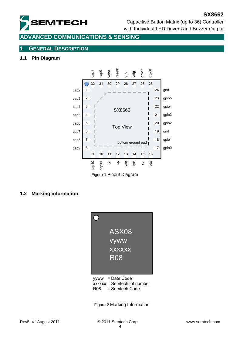
1.1 Pin Diagram
SX8662
Top View
1
2
3
4
5
6
7
8
24
23
22
21
20
19
18
17
9 10 11 12 13 14 15 16
2526272829303132
bottom ground pad
cap2
cap3
cap4
cap5
cap6
cap8
cap7
cap9
gnd
gpio5
gpio4
gpio3
gpio2
gpio1
gnd
gpio0
cap1
cap0
vana
resetb
gnd
gpio7
vdig
gpio6
cap10
cap11
cn
cp
vdd
scl
intb
sda
Figure 1 Pinout Diagram
1.2 Marking information
ASX08
yyww
xxxxxx
R08
yyww = Date Code
xxxxxx = Semtech lot number
R08 = Semtech Code
Figure 2 Marking Information
ADVANCED COMMUNICATIONS & SENSING
Rev5 4th August 2011 © 2011 Semtech Corp. www.semtech.com 5
SX8662 Capacitive Button Matrix (up to 36) Controller
with Individual LED Drivers and Buzzer Output
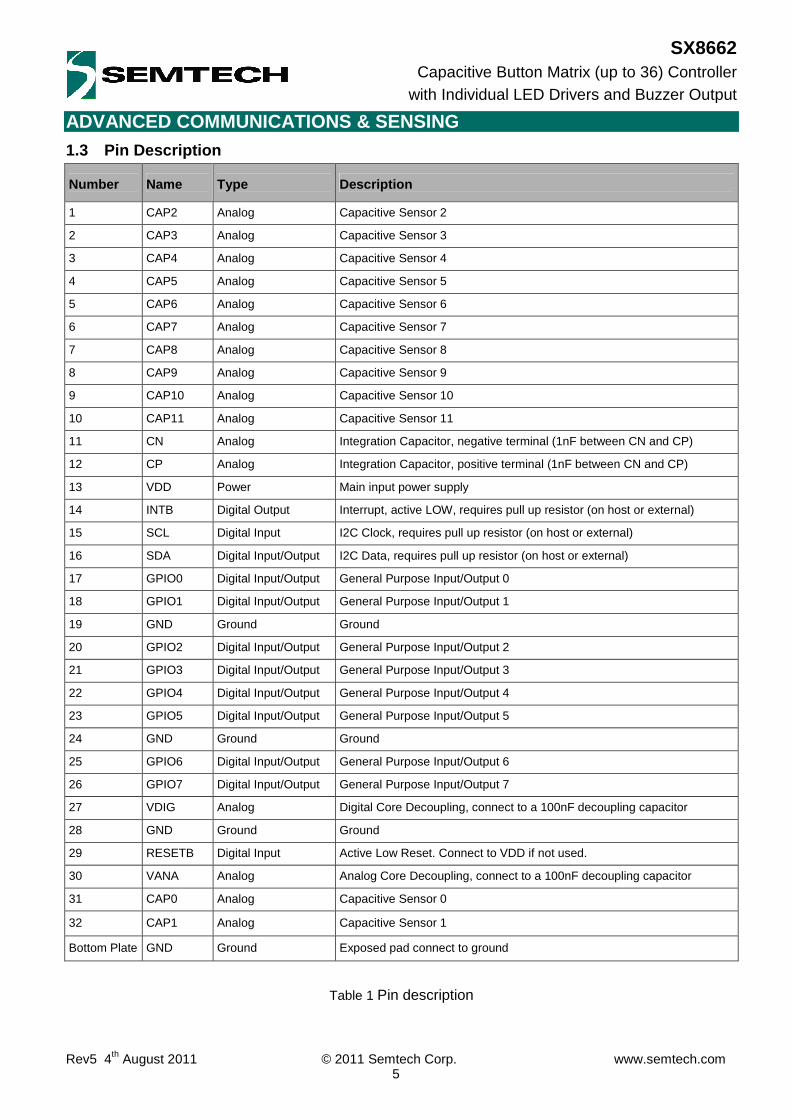
1.3 Pin Description
Number Name Type Description
1 CAP2 Analog Capacitive Sensor 2
2 CAP3 Analog Capacitive Sensor 3
3 CAP4 Analog Capacitive Sensor 4
4 CAP5 Analog Capacitive Sensor 5
5 CAP6 Analog Capacitive Sensor 6
6 CAP7 Analog Capacitive Sensor 7
7 CAP8 Analog Capacitive Sensor 8
8 CAP9 Analog Capacitive Sensor 9
9 CAP10 Analog Capacitive Sensor 10
10 CAP11 Analog Capacitive Sensor 11
11 CN Analog Integration Capacitor, negative terminal (1nF between CN and CP)
12 CP Analog Integration Capacitor, positive terminal (1nF between CN and CP)
13 VDD Power Main input power supply
14 INTB Digital Output Interrupt, active LOW, requires pull up resistor (on host or external)
15 SCL Digital Input I2C Clock, requires pull up resistor (on host or external)
16 SDA Digital Input/Output I2C Data, requires pull up resistor (on host or external)
17 GPIO0 Digital Input/Output General Purpose Input/Output 0
18 GPIO1 Digital Input/Output General Purpose Input/Output 1
19 GND Ground Ground
20 GPIO2 Digital Input/Output General Purpose Input/Output 2
21 GPIO3 Digital Input/Output General Purpose Input/Output 3
22 GPIO4 Digital Input/Output General Purpose Input/Output 4
23 GPIO5 Digital Input/Output General Purpose Input/Output 5
24 GND Ground Ground
25 GPIO6 Digital Input/Output General Purpose Input/Output 6
26 GPIO7 Digital Input/Output General Purpose Input/Output 7
27 VDIG Analog Digital Core Decoupling, connect to a 100nF decoupling capacitor
28 GND Ground Ground
29 RESETB Digital Input Active Low Reset. Connect to VDD if not used.
30 VANA Analog Analog Core Decoupling, connect to a 100nF decoupling capacitor
31 CAP0 Analog Capacitive Sensor 0
32 CAP1 Analog Capacitive Sensor 1
Bottom Plate GND Ground Exposed pad connect to ground
Table 1 Pin description

ADVANCED COMMUNICATIONS & SENSING
Rev5 4th August 2011 © 2011 Semtech Corp. www.semtech.com 6
SX8662 Capacitive Button Matrix (up to 36) Controller
with Individual LED Drivers and Buzzer Output
1.4 Simplified Block Diagram The simplified block diagram of the SX8662 is illustrated in Figure 3.
SX8662
cap2
cap3
cap4
cap5
cap6
cap8
cap7
cap9
gnd
gpio5
gpio4
gpio3
gpio2
gpio1
gnd
gpio0
cap1
cap0
vana
resetb
gnd
gpio7
vdig
gpio6
cap10
cap11
cn
cp
vdd
scl
intb
sda
analog
sensor
interface
micro
processor
RAM
ROM I2C
GPIO
controller
power management
clock
generation
RC
PWM
LED
controller
bottom plate
NVM
Figure 3 Simplified block diagram of the SX8662
1.5 Acronyms ASI Analog Sensor Interface DCV Digital Compensation Value GPO General Purpose Output GPP General Purpose PWM MTP Multiple Time Programmable NVM Non Volatile Memory PWM Pulse Width Modulation QSM Quick Start Memory SPM Shadow Parameter Memory SPO Special Purpose Output MK Matrix Key PK Priority Key PS Proximity Sensor TSM Tri-State Multiplexing

ADVANCED COMMUNICATIONS & SENSING
Rev5 4th August 2011 © 2011 Semtech Corp. www.semtech.com 7
SX8662 Capacitive Button Matrix (up to 36) Controller
with Individual LED Drivers and Buzzer Output
2 ELECTRICAL CHARACTERISTICS
2.1 Absolute Maximum Ratings Stresses above the values listed in “Absolute Maximum Ratings” may cause permanent damage to the device.
This is a stress rating only and functional operation of the device at these, or any other conditions beyond the “Recommended Operating Conditions”, is not implied. Exposure to absolute maximum rating conditions for extended periods may affect device reliability.
Parameter Symbol Min. Max. Unit
Supply Voltage VDD -0.5 3.9 V
Input voltage (non-supply pins) VIN -0.5 3.9 V
Input current (non-supply pins) IIN 10 mA
Operating Junction Temperature TJCT 125 °C
Reflow temperature TRE 260 °C
Storage temperature TSTOR -50 150 °C
ESD HBM (Human Body model)(i) ESDHBM 3 kV
Latchup(ii) ILU ± 100 mA
Table 2 Absolute Maximum Ratings
(i) Tested to JEDEC standard JESD22-A114
(ii) Tested to JEDEC standard JESD78
2.2 Recommended Operating Conditions
Parameter Symbol Min. Max. Unit
Supply Voltage VDD 2.7 3.6 V
Supply Voltage Drop(iii, iv, v) VDDdrop 100 mV
Supply Voltage for NVM programming VDD 3.0 3.6 V
Ambient Temperature Range TA -40 85 °C
Table 3 Recommended Operating Conditions
(iii) Performance for 2.6V < VDD < 2.7V might be degraded. (iv) Operation is not guaranteed below 2.6V. Should VDD briefly drop below this minimum value, then the SX8662 may require; - a hardware reset issued by the host using the RESETB pin
- a software reset issued by the host using the I2C interface (v) In the event the host processor is reset or undergoes a power OFF/ON cycle, it is recommended that the host also resets the SX8662 and assures that parameters are re-written into the SPM (should these differ to the parameters held in NVM).
2.3 Thermal Characteristics
Parameter Symbol Min. Max. Unit
Thermal Resistance - Junction to Ambient (vi) θJA 25 °C/W
Table 4 Thermal Characteristics
(vi) Static airflow

ADVANCED COMMUNICATIONS & SENSING
Rev5 4th August 2011 © 2011 Semtech Corp. www.semtech.com 8
SX8662 Capacitive Button Matrix (up to 36) Controller
with Individual LED Drivers and Buzzer Output
2.4 Electrical Specifications All values are valid within the operating conditions unless otherwise specified.
Parameter Symbol Conditions Min. Typ. Max. Unit
Current consumption
Active mode, average IOP,active 30ms scan period, 12 sensors enabled, minimum sensitivity
460 uA
Doze mode, average IOP,Doze 195ms scan period, 12 sensors enabled, minimum sensitivity
100 uA
Sleep IOP,sleep I2C listening, sensors disabled 8 17 uA
ResetB, SCL, SDA
Input logic high VIH 0.7*VDD VDD + 0.3 V
Input logic low VIL VSS applied to GND pins VSS - 0.3 0.8 V
Input leakage current LI CMOS input ±1 uA
Pull up resistor RPU when enabled 660 kΩ
Pull down resistor RPD when enabled 660 kΩ
GPIO set as Output, INTB, SDA
Output logic high VOH IOH<4mA VDD-0.4 V
Output logic low VOL
IOL,GPIO<12mA IOL,SDA,INTB<4mA
0.4 V
Start-up
Power up time tpor time between rising edge VDD and rising INTB 400 ms
RESETB
ResetB pulse width tres 50 ns
Recommended External components
capacitor between VDIG, GND Cvdig type 0402, tolerance +/-50% 100 nF
capacitor between VANA, GND Cvana type 0402, tolerance +/-50% 100 nF
capacitor between CP, CN Cint type 0402, COG, tolerance +/-5% 1 nF
capacitor between VDD, GND Cvdd type 0402, tolerance +/-50% 100 nF
Table 5 Electrical Specifications

ADVANCED COMMUNICATIONS & SENSING
Rev5 4th August 2011 © 2011 Semtech Corp. www.semtech.com 9
SX8662 Capacitive Button Matrix (up to 36) Controller
with Individual LED Drivers and Buzzer Output
Parameter Symbol Conditions Min. Typ. Max. Unit
I2C Timing Specifications (i)
SCL clock frequency fSCL 400 KHz
SCL low period tLOW 1.3 us
SCL high period tHIGH 0.6 us
Data setup time tSU;DAT 100 ns
Data hold time tHD;DAT 0 ns
Repeated start setup time tSU;STA 0.6 us
Start condition hold time tHD;STA 0.6 us
Stop condition setup time tSU;STO 0.6 us
Bus free time between stop and start tBUF 500 us
Input glitch suppression tSP 50 ns
Table 6 I2C Timing Specification
Notes: (i) All timing specifications, Figure 4 and Figure 5, refer to voltage levels (VIL, VIH, VOL) defined in Table 5. The interface complies with slave F/S mode as described by NXP: “I2C-bus specification, Rev. 03 - 19 June 2007”
Figure 4 I2C Start and Stop timing
Figure 5 I2C Data timing

ADVANCED COMMUNICATIONS & SENSING
Rev5 4th August 2011 © 2011 Semtech Corp. www.semtech.com 10
SX8662 Capacitive Button Matrix (up to 36) Controller
with Individual LED Drivers and Buzzer Output
3 FUNCTIONAL DESCRIPTION
3.1 Introduction
3.1.1 General
The SX8662 is intended to be used in applications which require capacitive sensors covered by isolating overlay material. A finger approaching the capacitive sensors will change the charge that can be loaded on the sensors. The SX8662 measures the change of charge and converts that into digital values (ticks). The larger the charge on the sensors, the larger the number of ticks will be. The charge to ticks conversion is done by the SX8662 Analog Sensor Interface (ASI). The ticks are further processed by the SX8662 and converted in a high level, easy to use information for the user’s host. The information between SX8662 and the host is passed through the I2C interface with an additional interrupt signal indicating that the SX8662 has new information. For buttons this information is simply touched or released. User feedback, done through the SX8662’s GPIOs, can be visual via LEDs and/or audio via a buzzer.
3.1.2 Parameters
The SX8662 has many low level built-in, fixed algorithms and procedures. To allow a lot of freedom for the user and adapt the SX8662 for different applications these algorithms and procedures can be configured with a large set of parameters which will be described in the following sections. Sensitivity and detection thresholds of the sensors are part of these parameters. Assuming that overlay material and sensors areas are identical then the sensitivities and thresholds will be the same for each sensor. In case sensors are not of the same size then sensitivities or thresholds might be chosen individually per sensor. So a smaller size sensor can have a larger sensitivity while a big size sensor may have the lower sensitivity.
3.1.3 Configuration
During a development phase the parameters can be determined and fine tuned by the users and downloaded over the I2C in a dynamic way. The parameter set can be downloaded over the I2C by the host each time the SX8662 boots up. This allows a flexible way of setting the parameters at the expense of I2C occupation. In case the parameters are frozen they can be programmed in Multiple Time Programmable (MTP) Non Volatile Memory (NVM) on the SX8662. The programming needs to be done once (over the I2C). The SX8662 will then boot up from the NVM and additional parameters from the host are not required anymore. In case the host desires to overwrite the boot-up NVM parameters (partly or even complete) this can be done by additional I2C communications.
3.2 Scan Period
The basic operation Scan period of the SX8662 sensing interface can be split into three periods over time.
In the first period (Sensing) the SX8662 is sensing all enabled CAP inputs, from CAP0 towards CAP11.
In the second period (Processing) the SX8662 processes the sensor data, verifies and updates the GPIO and the I2C.
In the third period (Timer) the SX8662 is set in a low power mode and waits until a new cycle starts.
Figure 6 shows the different SX8662 periods over time.

ADVANCED COMMUNICATIONS & SENSING
Rev5 4th August 2011 © 2011 Semtech Corp. www.semtech.com 11
SX8662 Capacitive Button Matrix (up to 36) Controller
with Individual LED Drivers and Buzzer Output
Figure 6 Scan Period
The scan period determines the minimum reaction time of the SX8662. The scan period can be configured by the host from 15ms to values larger than a second. The reaction time is defined as the interval between a touch on the sensor and the moment that the SX8662 generates the interrupt on the INTB pin. The shorter the scan period the faster the reaction time will be. Very low power consumptions can be obtained by setting very long scan periods with the expense of having longer reaction times. All external events like GPIO, I2C and the interrupt are updated in the processing period, so once every scan period.
3.3 Operation modes The SX8662 has 3 operation modes. The main difference is found in the reaction time (corresponding to the scan period) and power consumption. Active mode offers fast scan periods. The typical reaction time is 30ms. All enabled sensors are scanned and information data is processed within this interval. Doze mode increases the scan period time which increases the reaction time to 195ms typical and at the same time reduces the operating current. Sleep mode turns the SX8662 OFF, except for the I2C peripheral, minimizing operating current while maintaining the power supplies. In Sleep mode the SX8662 does not do any sensor scanning. The Sleep mode will be exited by any I2C access. The user can specify other scan periods for the Active and Doze mode and decide for other compromises between reaction time and power consumption. In most applications the reaction time needs to be fast when fingers are present, but can be slow when no person uses the application. In case the SX8662 is not used for a specific time it will go from Active mode into Doze mode and power will be saved. This time-out is determined by the Passive Timer which can be configured by the user or turned OFF if not required. To leave Doze mode and enter Active mode this can be done by a simple touch on any button. The host can decide to force the operating mode by issuing commands over the I2C (using register CompOpMode) and take fully control of the SX8662. The diagram in Figure 7 shows the available operation modes and the possible transitions.

ADVANCED COMMUNICATIONS & SENSING
Rev5 4th August 2011 © 2011 Semtech Corp. www.semtech.com 12
SX8662 Capacitive Button Matrix (up to 36) Controller
with Individual LED Drivers and Buzzer Output
Figure 7 Operation modes
3.4 Sensors on the PCB
3.4.1 Matrix Keys/Buttons (MK)
In opposition to most of the other Semtech capacitive sensing products where 1 button = 1 sensor (CAP0…CAP11)., the SX8662 requires sensors to be routed in matrix and each button is formed by the intersection/concatenation of two sensors areas. The buttons are covered by isolating overlay material (typically 1mm...3mm). The area of a button is typically one square centimetre which corresponds about to the area of a finger touching the overlay material.
Figure 8 Matrix buttons layout/connections (Red = Top; Brown = Inner1; Blue = Inner2)
IMPORTANT: Please note that while the matrix structure allows increasing dramatically the potential maximum number of buttons (up to 36 with only 12 sensors) it also limits the operation to max one matrix button reported at a time (ie single button touch operation). When several matrix buttons are touched only the first one is reported.
3.4.2 Priority Key/Button (PK)
When the priority key is enabled in BtnCfg[6], CAP11 can be routed outside the matrix to a separate standard button sensor. Matrix size is then reduced to 6x5 keys (CAP0…CAP10). Priority key operation/reporting is independent from the matrix and can be used for any “high priority” key (Power, Reset, etc) or “multi-touch” function (Shift, Alt, etc).
3.4.3 Schematics Requirements For each PK combination, a specific schematic must be followed on the board as illustrated in figure below.
ADVANCED COMMUNICATIONS & SENSING
Rev5 4th August 2011 © 2011 Semtech Corp. www.semtech.com 13
SX8662 Capacitive Button Matrix (up to 36) Controller
with Individual LED Drivers and Buzzer Output
CA
P0
CA
P10
CAP4
CAP5
CA
P8
CAP11
PK = OFF
CA
P3
CA
P2
CA
P1
CAP6
CAP9
CAP7
MK1
MK2
MK5
MK10
MK17
MK26
MK4
MK3
MK6
MK11
MK18
MK27
MK8
MK7
MK12
MK19
MK28
MK16
MK15
MK14
MK13
MK20
MK29
MK25
MK24
MK23
MK22
MK21
MK30
MK36
MK35
MK34
MK33
MK32
MK31
MK9
CA
P0
CA
P10
CAP4
CAP5
CA
P8
PK = ON (CAP11)
CA
P3
CA
P2
CA
P1
CAP6
CAP9
CAP7
MK1
MK2
MK5
MK10
MK17
MK26
MK4
MK3
MK6
MK11
MK18
MK27
MK8
MK7
MK12
MK19
MK28
MK16
MK15
MK14
MK13
MK20
MK29
MK25
MK24
MK23
MK22
MK21
MK30
MK9
Figure 9 Sensors Schematics Requirements vs Configuration

ADVANCED COMMUNICATIONS & SENSING
Rev5 4th August 2011 © 2011 Semtech Corp. www.semtech.com 14
SX8662 Capacitive Button Matrix (up to 36) Controller
with Individual LED Drivers and Buzzer Output
3.5 Button Information (MK and PK) The touch buttons have two simple states (see Figure 10): ON (touched by finger) and OFF (released and no finger press).
Figure 10 Buttons
A finger touch is reported as soon as the ASI ticks of both sensors forming the button exceed their user-defined threshold plus a hysteresis.
A finger release is reported as soon as the ASI ticks of one at least of the sensors forming the button goes below its user-defined threshold minus a hysteresis.
The hysteresis around the threshold avoids rapid touch and release signalling during transients. IMPORTANT: Please note that while the matrix structure allows increasing dramatically the potential maximum number of buttons (up to 36 with only 12 sensors) it also limits the operation to max one matrix button reported at a time (ie single button touch operation). When two matrix buttons are touched only the first one is reported.
3.6 Analog Sensing Interface
The Analog Sensing Interface (ASI) converts the charge on the sensors into ticks which will be further digitally processed. The basic principle of the ASI will be explained in this section.
The ASI consists of a multiplexer selecting the sensor, analog switches, a reference voltage, an ADC sigma delta converter, an offset compensation DAC and an external integration capacitor (see Figure 11).
Figure 11 Analog Sensor Interface
To get the ticks representing the charge on a specific sensor the ASI will execute several steps.

ADVANCED COMMUNICATIONS & SENSING
Rev5 4th August 2011 © 2011 Semtech Corp. www.semtech.com 15
SX8662 Capacitive Button Matrix (up to 36) Controller
with Individual LED Drivers and Buzzer Output
The charge on a sensor cap (e.g CAP0) will be accumulated multiple times on the external integration capacitor, Cint.
This results in an increasing voltage on Cint proportional to the capacitance on CAP0.
At this stage the offset compensation DAC is enabled. The compensation DAC generates a voltage proportional to an estimation of the external capacitance. The estimation is obtained by the offset compensation procedure executed e.g. at power-up.
The difference between the DAC output and the charge on Cint is the desired signal. In the ideal case the difference of charge will be converted to zero ticks if no finger is present and the number of ticks becomes high in case a finger is present.
The difference of charge on Cint and the DAC output will be transferred to the ADC (Sigma Delta Integrator).
After the charge transfer to the ADC the steps above will be repeated.
The larger the number the cycles are repeated the larger the signal out of the ADC with improved SNR. The sensitivity is therefore directly related to the number of cycles.
The SX8662 allows setting the sensitivity for each sensor individually in applications which have a variety of sensors sizes or different overlays or for fine-tuning performances. The optimal sensitivity is depending heavily on the final application. If the sensitivity is too low the ticks will not pass the thresholds and user detection will not be possible. In case the sensitivity is set too large, some power will be wasted and false touch information may be output (i.e. for touch buttons => finger not touching yet).
Once the ASI has finished the first sensor, the ticks are stored and the ASI will start measuring the next sensor until all (enabled) sensors pins have been treated.
In case some sensors are disabled then these result in lower power consumption simply because the ASI is active for a shorter period and the following processing period will be shorter.
The ticks from the ASI will then be handled by the digital processing.
The ASI will shut down and wait until new sensing period will start.

ADVANCED COMMUNICATIONS & SENSING
Rev5 4th August 2011 © 2011 Semtech Corp. www.semtech.com 16
SX8662 Capacitive Button Matrix (up to 36) Controller
with Individual LED Drivers and Buzzer Output
3.7 Offset Compensation
The capacitance at the CAP pins is determined by an intrinsic capacitance of the integrated circuit, the PCB traces, ground coupling and the sensor planes. This capacitance is relatively large and might become easily some tens of pF. This parasitic capacitance will vary only slowly over time due to environmental changes.
A finger touch is in the order of one pF. If the finger approaches the sensor this occurs typically fast.
The ASI has the difficult task to detect and distinguish a small, fast changing capacitance, from a large, slow varying capacitance. This would require a very precise, high resolution ADC and complicated, power consuming, digital processing.
The SX8662 features a 16 bit DAC which compensates for the large, slow varying capacitance already in front of the ADC. In other words the ADC converts only the desired small signal. In the ideal world the ADC will put out zero ticks even if the external capacitance is as high as 100pF.
At each power-up of the SX8662 the Digital Compensation Values (DCV) are estimated by the digital processing algorithms. The algorithm will adjust the compensation values such that zero ticks will be generated by the ADC.
Once the correct compensation values are found these will be stored and used to compensate each CAP pin.
If the SX8662 is shut down the compensation values will be lost. At a next power-up the procedure starts all over again. This assures that the SX8662 will operate under any condition. Powering up at e.g. different temperatures will not change the performance of the SX8662 and the host does not have to do anything special.
The DCVs do not need to be updated if the external conditions remain stable.
However if e.g. temperature changes this will influence the external capacitance. The ADC ticks will drift then slowly around zero values basically because of the mismatch of the compensation circuitry and the external capacitance.
In case the average value of the ticks become higher than the positive noise threshold (configurable by user) or lower than the negative threshold (configurable by user) then the SX8662 will initiate a compensation procedure and find a new set of DCVs.
Compensation procedures can as well be initiated by the SX8662 on periodic intervals. Even if the ticks remain within the positive and negative noise thresholds the compensation procedure will then estimate new sets of DCVs.
Finally the host can initiate a compensation procedure by using the I2C interface. This is e.g. required after the host changed the sensitivity of sensors.

ADVANCED COMMUNICATIONS & SENSING
Rev5 4th August 2011 © 2011 Semtech Corp. www.semtech.com 17
SX8662 Capacitive Button Matrix (up to 36) Controller
with Individual LED Drivers and Buzzer Output
3.8 Processing The first processing step of the raw ticks, coming out of the ASI, is low pass filtering to obtain an estimation of the average capacitance: tick-ave (see Figure 12). This slowly varying average is important in the detection of slowly changing environmental changes.
ticks (raw)
compensation DCV
ASI processing
low pass
tick-diff
tick-ave
processing
GPIO
controller
PWM LED
controller
I2C
SPM
Figure 12 Processing
The difference of the tick average and the raw ticks, tick-diff, is a good estimation of rapid changing input capacitances.
The tick-diff, tick-ave and the configuration parameters in the SPM are then processed and determines the sensor information, I2C registers status and PWM control.
3.9 Configuration
Figure 13 shows the building blocks used for configuring the SX8662.
Figure 13 Configuration
The default configuration parameters of the SX8662 are stored in the Quick Start Memory (QSM). This configuration data is setup to a very common application for the SX8662 with 8 buttons. Without any programming or host interaction the SX8662 will start up in the Quick Start Application.
The QSM settings are fixed and cannot be changed by the user.

ADVANCED COMMUNICATIONS & SENSING
Rev5 4th August 2011 © 2011 Semtech Corp. www.semtech.com 18
SX8662 Capacitive Button Matrix (up to 36) Controller
with Individual LED Drivers and Buzzer Output
In case the application needs different settings than the QSM settings then the SX8662 can be setup and/or programmed over the I2C interface.
The configuration parameters of the SX8662 can be stored in the Multiple Time Programmable (MTP) Non Volatile Memory (NVM). The NVM contains all those parameters that are defined and stable for the application. Examples are the number of sensors enabled, sensitivity, active and Doze scan period. The details of these parameters are described in the next chapters.
At power up the SX8662 checks if the NVM contains valid data. In that case the configuration parameter source becomes the NVM. If the NVM is empty or non-valid then the configuration source becomes the QSM. In the next step the SX8662 copies the configuration parameter source into the Shadow Parameter Memory (SPM). The SX8662 is operational and uses the configuration parameters of the SPM.
During power down or reset event the SPM loses all content. It will automatically be reloaded following power up or at the end of the reset event.
The host will interface with the SX8662 through the I2C bus and the analog output interface.
The I2C of the SX8662 consists of 16 registers. Some of these I2C registers are used to read the status and information of the buttons. Other I2C registers allow the host to take control of the SX8662. The host can e.g. decide to change the operation mode from active mode to Doze mode or go into sleep (according Figure 7).
Two additional modes allow the host to have an access to the SPM or indirect access to the NVM.
These modes are required during development, can be used in real time or in-field programming.
Figure 14 shows the Host SPM mode. In this mode the host can decide to overwrite the SPM. This is useful during the development phases of the application where the configuration parameters are not yet fully defined and as well during the operation of the application if some parameters need small deviations from the QSM or NVM content.
Figure 14 Host SPM mode
The content of the SPM remains valid as long as the SX8662 is powered. After a power down the host needs to re-write the SPM at the next power-up.
Figure 15 shows the Host NVM mode. In this mode the host will be able to write the NVM.
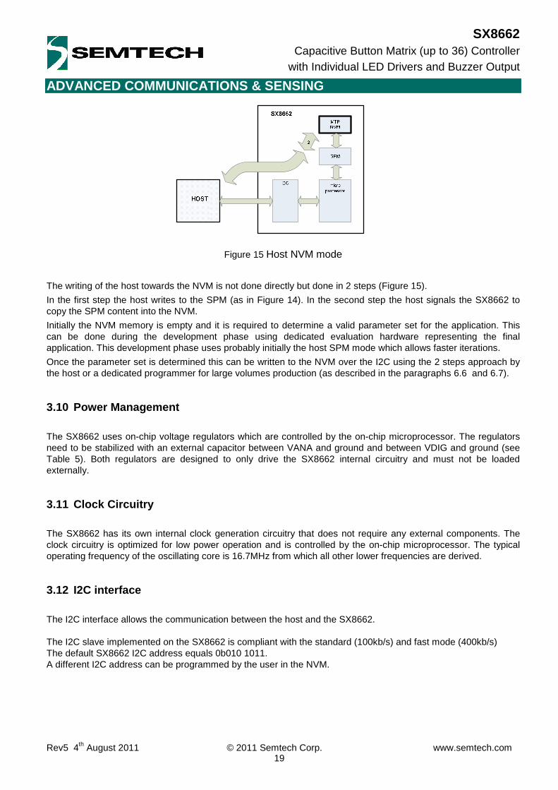
ADVANCED COMMUNICATIONS & SENSING
Rev5 4th August 2011 © 2011 Semtech Corp. www.semtech.com 19
SX8662 Capacitive Button Matrix (up to 36) Controller
with Individual LED Drivers and Buzzer Output
Figure 15 Host NVM mode
The writing of the host towards the NVM is not done directly but done in 2 steps (Figure 15).
In the first step the host writes to the SPM (as in Figure 14). In the second step the host signals the SX8662 to copy the SPM content into the NVM.
Initially the NVM memory is empty and it is required to determine a valid parameter set for the application. This can be done during the development phase using dedicated evaluation hardware representing the final application. This development phase uses probably initially the host SPM mode which allows faster iterations.
Once the parameter set is determined this can be written to the NVM over the I2C using the 2 steps approach by the host or a dedicated programmer for large volumes production (as described in the paragraphs 6.6 and 6.7).
3.10 Power Management
The SX8662 uses on-chip voltage regulators which are controlled by the on-chip microprocessor. The regulators need to be stabilized with an external capacitor between VANA and ground and between VDIG and ground (see Table 5). Both regulators are designed to only drive the SX8662 internal circuitry and must not be loaded externally.
3.11 Clock Circuitry
The SX8662 has its own internal clock generation circuitry that does not require any external components. The clock circuitry is optimized for low power operation and is controlled by the on-chip microprocessor. The typical operating frequency of the oscillating core is 16.7MHz from which all other lower frequencies are derived.
3.12 I2C interface
The I2C interface allows the communication between the host and the SX8662. The I2C slave implemented on the SX8662 is compliant with the standard (100kb/s) and fast mode (400kb/s) The default SX8662 I2C address equals 0b010 1011. A different I2C address can be programmed by the user in the NVM.
ADVANCED COMMUNICATIONS & SENSING
Rev5 4th August 2011 © 2011 Semtech Corp. www.semtech.com 20
SX8662 Capacitive Button Matrix (up to 36) Controller
with Individual LED Drivers and Buzzer Output
3.13 Interrupt
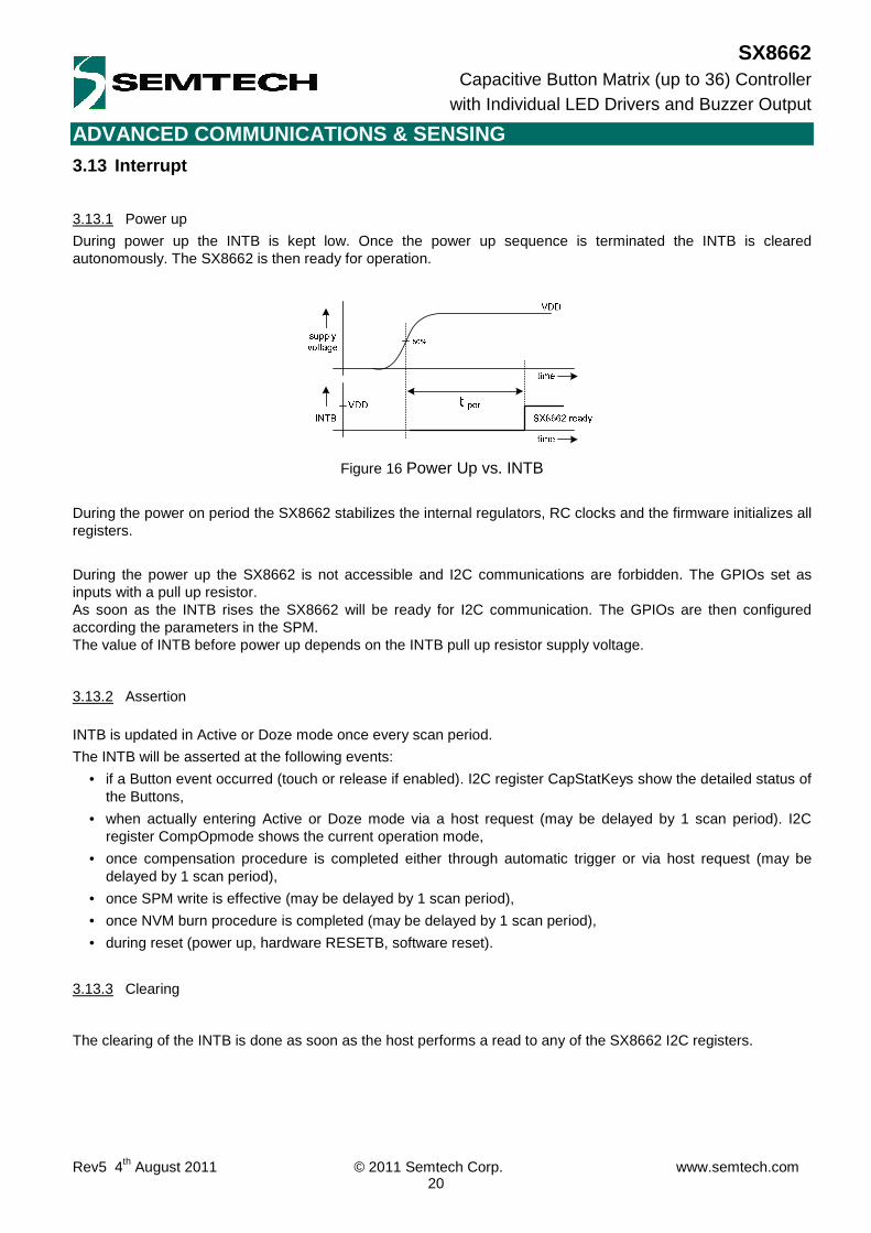
3.13.1 Power up
During power up the INTB is kept low. Once the power up sequence is terminated the INTB is cleared autonomously. The SX8662 is then ready for operation.
Figure 16 Power Up vs. INTB
During the power on period the SX8662 stabilizes the internal regulators, RC clocks and the firmware initializes all registers.
During the power up the SX8662 is not accessible and I2C communications are forbidden. The GPIOs set as inputs with a pull up resistor. As soon as the INTB rises the SX8662 will be ready for I2C communication. The GPIOs are then configured according the parameters in the SPM. The value of INTB before power up depends on the INTB pull up resistor supply voltage.
3.13.2 Assertion INTB is updated in Active or Doze mode once every scan period.
The INTB will be asserted at the following events:
• if a Button event occurred (touch or release if enabled). I2C register CapStatKeys show the detailed status of the Buttons,
• when actually entering Active or Doze mode via a host request (may be delayed by 1 scan period). I2C register CompOpmode shows the current operation mode,
• once compensation procedure is completed either through automatic trigger or via host request (may be delayed by 1 scan period),
• once SPM write is effective (may be delayed by 1 scan period),
• once NVM burn procedure is completed (may be delayed by 1 scan period),
• during reset (power up, hardware RESETB, software reset).
3.13.3 Clearing
The clearing of the INTB is done as soon as the host performs a read to any of the SX8662 I2C registers.

ADVANCED COMMUNICATIONS & SENSING
Rev5 4th August 2011 © 2011 Semtech Corp. www.semtech.com 21
SX8662 Capacitive Button Matrix (up to 36) Controller
with Individual LED Drivers and Buzzer Output
3.13.4 Example
A typical example of the assertion and clearing of the INTB and the I2C communication is shown in Figure 17.
Figure 17 Interrupt and I2C
When a button is touched the SX8662 will assert the interrupt (1). The host will read the SX8662 status information over the I2C (2) and this clears the interrupt.
If the finger releases the button the interrupt will be asserted (3), the host reads the status (4) which clears the interrupt.
In case the host will not react to an interrupt then this will result in a missing touch.
3.14 Reset
The reset can be performed by 3 sources:
- power up,
- RESETB pin,
- software reset.
3.14.1 Power up
During power up the INTB is kept low. Once the power up sequence is terminated the INTB is released autonomously. The SX8662 is then ready for operation.
Figure 18 Power Up vs. INTB
ADVANCED COMMUNICATIONS & SENSING
Rev5 4th August 2011 © 2011 Semtech Corp. www.semtech.com 22
SX8662 Capacitive Button Matrix (up to 36) Controller
with Individual LED Drivers and Buzzer Output
During the power on period the SX8662 stabilizes the internal regulators, RC clocks and the firmware initializes all registers.
During the power up the SX8662 is not accessible and I2C communications are forbidden. As soon as the INTB rises the SX8662 will be ready for I2C communication.
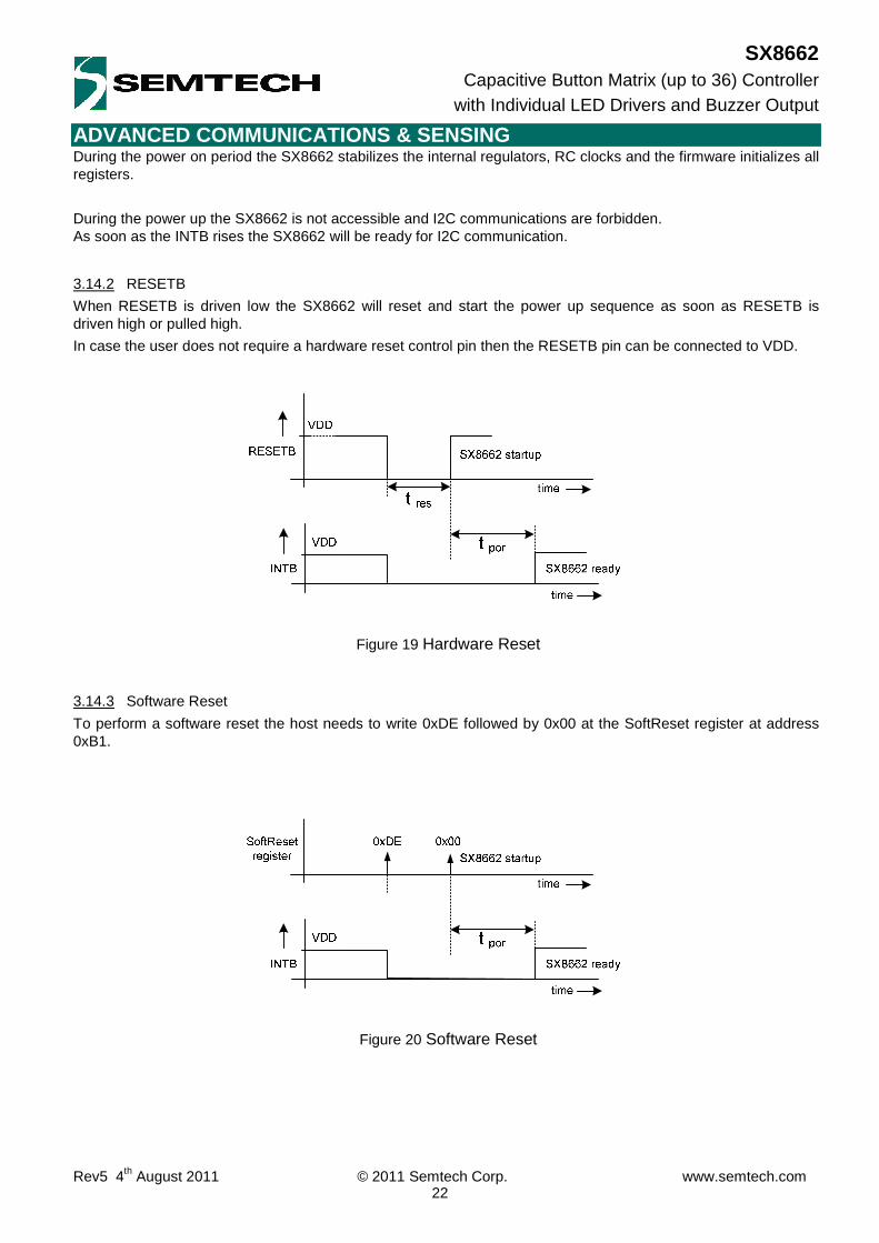
3.14.2 RESETB
When RESETB is driven low the SX8662 will reset and start the power up sequence as soon as RESETB is driven high or pulled high.
In case the user does not require a hardware reset control pin then the RESETB pin can be connected to VDD.
Figure 19 Hardware Reset
3.14.3 Software Reset
To perform a software reset the host needs to write 0xDE followed by 0x00 at the SoftReset register at address 0xB1.
Figure 20 Software Reset
ADVANCED COMMUNICATIONS & SENSING
Rev5 4th August 2011 © 2011 Semtech Corp. www.semtech.com 23
SX8662 Capacitive Button Matrix (up to 36) Controller
with Individual LED Drivers and Buzzer Output
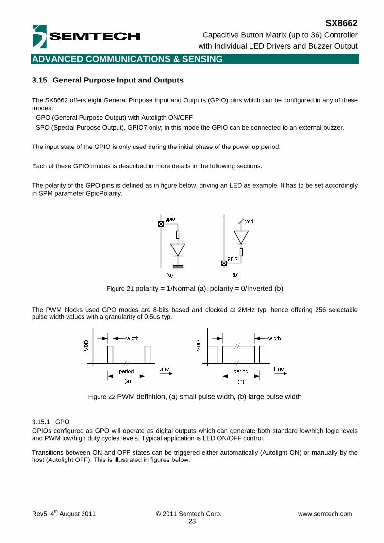
3.15 General Purpose Input and Outputs
The SX8662 offers eight General Purpose Input and Outputs (GPIO) pins which can be configured in any of these modes:
- GPO (General Purpose Output) with Autoligth ON/OFF
- SPO (Special Purpose Output). GPIO7 only; in this mode the GPIO can be connected to an external buzzer.
The input state of the GPIO is only used during the initial phase of the power up period.
Each of these GPIO modes is described in more details in the following sections.
The polarity of the GPO pins is defined as in figure below, driving an LED as example. It has to be set accordingly in SPM parameter GpioPolarity.
Figure 21 polarity = 1/Normal (a), polarity = 0/Inverted (b)
The PWM blocks used GPO modes are 8-bits based and clocked at 2MHz typ. hence offering 256 selectable pulse width values with a granularity of 0.5us typ.
Figure 22 PWM definition, (a) small pulse width, (b) large pulse width
3.15.1 GPO GPIOs configured as GPO will operate as digital outputs which can generate both standard low/high logic levels and PWM low/high duty cycles levels. Typical application is LED ON/OFF control. Transitions between ON and OFF states can be triggered either automatically (Autolight ON) or manually by the host (Autolight OFF). This is illustrated in figures below.

ADVANCED COMMUNICATIONS & SENSING
Rev5 4th August 2011 © 2011 Semtech Corp. www.semtech.com 24
SX8662 Capacitive Button Matrix (up to 36) Controller
with Individual LED Drivers and Buzzer Output
Figure 23 LED Control in GPO mode, Autolight OFF
Figure 24 LED Control in GPO mode, Autolight ON
Additionally these transitions can be configured to be done with or without fading following a logarithmic or linear function. This is illustrated in figures below.
Figure 25 GPO ON transition (LED fade in), normal polarity, (a) linear, (b) logarithmic
Figure 26 GPO ON transition (LED fade in), inverted polarity, (a) linear, (b) logarithmic
The fading out (e.g. after a button is released) is identical to the fading in but an additional off delay can be added before the fading starts (Figure 27 and Figure 28).

ADVANCED COMMUNICATIONS & SENSING
Rev5 4th August 2011 © 2011 Semtech Corp. www.semtech.com 25
SX8662 Capacitive Button Matrix (up to 36) Controller
with Individual LED Drivers and Buzzer Output
Figure 27 GPO OFF transition (LED fade out), normal polarity, (a) linear, (b) logarithmic
Figure 28 GPO OFF transition (LED fade out), inverted polarity, (a) linear, (b) logarithmic
Please note that standard high/low logic signals are just a specific case of GPO mode and can also be generated simply by setting inc/dec time to 0 (i.e. OFF) and programming intensity OFF/ON to 0x00 and 0xFF.
3.15.2 Fading Modes The SX8662 supports two different fading modes, namely Single and Continuous. These fading modes can be configured for each GPIO individually. Please see 5.6 “GPIO Parameters” for more information on how to configure this feature.
i) Single Fading Mode:
The GPO pin fades in when the associated button is touched and it fades out when it is released. This is shown in Figure 29
fading-in
OFF intensity
ON intensity
delay_off fading-out
OFF intensity
ON
OFF
OFF
Figure 29 Single Fading Mode
ii) Continuous Fading Mode:

ADVANCED COMMUNICATIONS & SENSING
Rev5 4th August 2011 © 2011 Semtech Corp. www.semtech.com 26
SX8662 Capacitive Button Matrix (up to 36) Controller
with Individual LED Drivers and Buzzer Output
The GPO pin fades in and fades out continuously when the associated button is touched. The fading in and out stops when the button is released. This is shown in Figure 30.
fading-in
OFF intensity
ON intensity
fading-out
OFF intensity
ON
OFF
Figure 30 Continuous Fading Mode
3.15.3 Intensity index vs PWM pulse width Tables below are used to convert all intensity indexes parameters GpioIntensityOff, GpioIntensityOn and GppIntensity but also to generate fading in GPO mode During fading in(out), the index is automatically incremented(decremented) at every Inc(Dec)Time x Inc(Dec)Factor until it reaches the programmed GpioIntensityOn(Off) value. Index Lin/Log Index Lin/Log Index Lin/Log Index Lin/Log Index Lin/Log Index Lin/Log Index Lin/Log Index Lin/Log
0 0/0 32 33/5 64 65/12 96 97/26 128 129/48 160 161/81 192 193/125 224 225/184 1 2/0 33 34/5 65 66/13 97 98/27 129 130/49 161 162/82 193 194/127 225 226/186 2 3/0 34 35/5 66 67/13 98 99/27 130 131/50 162 163/83 194 195/129 226 227/188 3 4/0 35 36/5 67 68/13 99 100/28 131 132/51 163 164/84 195 196/130 227 228/190 4 5/0 36 37/5 68 69/14 100 101/29 132 133/52 164 165/86 196 197/132 228 229/192 5 6/2 37 38/6 69 70/14 101 102/29 133 134/53 165 166/87 197 198/133 229 230/194 6 7/2 38 39/6 70 71/14 102 103/30 134 135/54 166 167/88 198 199/135 230 231/197 7 8/2 39 40/6 71 72/15 103 104/30 135 136/55 167 168/89 199 200/137 231 232/199 8 9/2 40 41/6 72 73/15 104 105/31 136 137/55 168 169/91 200 201/139 232 233/201 9 10/2 41 42/6 73 74/15 105 106/32 137 138/56 169 170/92 201 202/140 233 234/203
10 11/2 42 43/7 74 75/16 106 107/32 138 139/57 170 171/93 202 203/142 234 235/205 11 12/2 43 44/7 75 76/16 107 108/33 139 140/58 171 172/95 203 204/144 235 236/208 12 13/2 44 45/7 76 77/16 108 109/33 140 141/59 172 173/96 204 205/146 236 237/210 13 14/2 45 46/7 77 78/17 109 110/34 141 142/60 173 174/97 205 206/147 237 238/212 14 15/3 46 47/7 78 79/17 110 111/35 142 143/61 174 175/99 206 207/149 238 239/215 15 16/3 47 48/8 79 80/18 111 112/35 143 144/62 175 176/100 207 208/151 239 240/217 16 17/3 48 49/8 80 81/18 112 113/36 144 145/63 176 177/101 208 209/153 240 241/219 17 18/3 49 50/8 81 82/19 113 114/37 145 146/64 177 178/103 209 210/155 241 242/221 18 19/3 50 51/8 82 83/19 114 115/38 146 147/65 178 179/104 210 211/156 242 243/224 19 20/3 51 52/9 83 84/20 115 116/38 147 148/66 179 180/106 211 212/158 243 244/226 20 21/3 52 53/9 84 85/20 116 117/39 148 149/67 180 181/107 212 213/160 244 245/229 21 22/3 53 54/9 85 86/21 117 118/40 149 150/68 181 182/109 213 214/162 245 246/231 22 23/3 54 55/9 86 87/21 118 119/40 150 151/69 182 183/110 214 215/164 246 247/233 23 24/4 55 56/10 87 88/22 119 120/41 151 152/71 183 184/111 215 216/166 247 248/236 24 25/4 56 57/10 88 89/22 120 121/42 152 153/72 184 185/113 216 217/168 248 249/238 25 26/4 57 58/10 89 90/23 121 122/43 153 154/73 185 186/114 217 218/170 249 250/241 26 27/4 58 59/10 90 91/23 122 123/44 154 155/74 186 187/116 218 219/172 250 251/243 27 28/4 59 60/11 91 92/24 123 124/44 155 156/75 187 188/117 219 220/174 251 252/246 28 29/4 60 61/11 92 93/24 124 125/45 156 157/76 188 189/119 220 221/176 252 253/248 29 30/4 61 62/11 93 94/25 125 126/46 157 158/77 189 190/121 221 222/178 253 254/251 30 31/4 62 63/12 94 95/25 126 127/47 158 159/78 190 191/122 222 223/180 254 255/253 31 32/5 63 64/12 95 96/26 127 128/48 159 160/80 191 192/124 223 224/182 255 256/256
Table 7 Intensity index vs. PWM pulse width (normal polarity)
Index Lin/Log Index Lin/Log Index Lin/Log Index Lin/Log Index Lin/Log Index Lin/Log Index Lin/Log Index Lin/Log
0 256/256 32 224/251 64 192/244 96 160/230 128 128/208 160 96/175 192 64/131 224 32/72 1 255/256 33 223/251 65 191/243 97 159/229 129 127/207 161 95/174 193 63/129 225 31/70
ADVANCED COMMUNICATIONS & SENSING
Rev5 4th August 2011 © 2011 Semtech Corp. www.semtech.com 27
SX8662 Capacitive Button Matrix (up to 36) Controller
with Individual LED Drivers and Buzzer Output
2 254/256 34 222/251 66 190/243 98 158/229 130 126/206 162 94/173 194 62/127 226 30/68 3 253/256 35 221/251 67 189/243 99 157/228 131 125/205 163 93/172 195 61/126 227 29/66 4 252/256 36 220/251 68 188/242 100 156/227 132 124/204 164 92/170 196 60/124 228 28/64 5 251/254 37 219/250 69 187/242 101 155/227 133 123/203 165 91/169 197 59/123 229 27/62 6 250/254 38 218/250 70 186/242 102 154/226 134 122/202 166 90/168 198 58/121 230 26/59 7 249/254 39 217/250 71 185/241 103 153/226 135 121/201 167 89/167 199 57/119 231 25/57 8 248/254 40 216/250 72 184/241 104 152/225 136 120/201 168 88/165 200 56/117 232 24/55 9 247/254 41 215/250 73 183/241 105 151/224 137 119/200 169 87/164 201 55/116 233 23/53
10 246/254 42 214/249 74 182/240 106 150/224 138 118/199 170 86/163 202 54/114 234 22/50 11 245/254 43 213/249 75 181/240 107 149/223 139 117/198 171 85/161 203 53/112 235 21/48 12 244/254 44 212/249 76 180/240 108 148/223 140 116/197 172 84/160 204 52/110 236 20/46 13 243/254 45 211/249 77 179/239 109 147/222 141 115/196 173 83/159 205 51/109 237 19/44 14 242/253 46 210/249 78 178/239 110 146/221 142 114/195 174 82/157 206 50/107 238 18/41 15 241/253 47 209/248 79 177/238 111 145/221 143 113/194 175 81/156 207 49/105 239 17/39 16 240/253 48 208/248 80 176/238 112 144/220 144 112/193 176 80/155 208 48/103 240 16/37 17 239/253 49 207/248 81 175/237 113 143/219 145 111/192 177 79/153 209 47/101 241 15/35 18 238/253 50 206/248 82 174/237 114 142/218 146 110/191 178 78/152 210 46/100 242 14/32 19 237/253 51 205/247 83 173/236 115 141/218 147 109/190 179 77/150 211 45/98 243 13/30 20 236/253 52 204/247 84 172/236 116 140/217 148 108/189 180 76/149 212 44/96 244 12/27 21 235/253 53 203/247 85 171/235 117 139/216 149 107/188 181 75/147 213 43/94 245 11/25 22 234/253 54 202/247 86 170/235 118 138/216 150 106/187 182 74/146 214 42/92 246 10/23 23 233/252 55 201/246 87 169/234 119 137/215 151 105/185 183 73/145 215 41/90 247 9/20 24 232/252 56 200/246 88 168/234 120 136/214 152 104/184 184 72/143 216 40/88 248 8/18 25 231/252 57 199/246 89 167/233 121 135/213 153 103/183 185 71/142 217 39/86 249 7/15 26 230/252 58 198/246 90 166/233 122 134/212 154 102/182 186 70/140 218 38/84 250 6/13 27 229/252 59 197/245 91 165/232 123 133/212 155 101/181 187 69/139 219 37/82 251 5/10 28 228/252 60 196/245 92 164/232 124 132/211 156 100/180 188 68/137 220 36/80 252 4/8 29 227/252 61 195/245 93 163/231 125 131/210 157 99/179 189 67/135 221 35/78 253 3/5 30 226/252 62 194/244 94 162/231 126 130/209 158 98/178 190 66/134 222 34/76 254 2/3 31 225/251 63 193/244 95 161/230 127 129/208 159 97/176 191 65/132 223 33/74 255 0/0
Table 8 Intensity index vs. PWM pulse width (inverted polarity)
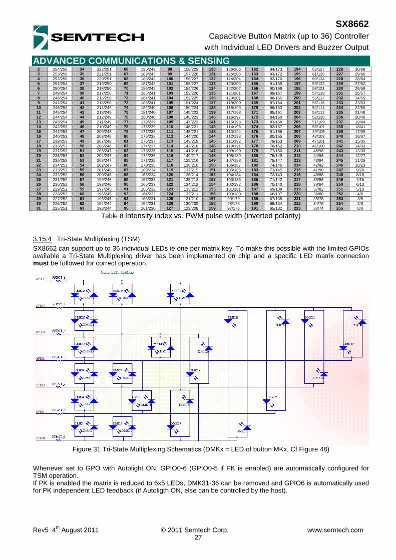
3.15.4 Tri-State Multiplexing (TSM) SX8662 can support up to 36 individual LEDs ie one per matrix key. To make this possible with the limited GPIOs available a Tri-State Multiplexing driver has been implemented on chip and a specific LED matrix connection must be followed for correct operation.
Figure 31 Tri-State Multiplexing Schematics (DMKx = LED of button MKx, Cf Figure 48)
Whenever set to GPO with Autolight ON, GPIO0-6 (GPIO0-5 if PK is enabled) are automatically configured for TSM operation. If PK is enabled the matrix is reduced to 6x5 LEDs, DMK31-36 can be removed and GPIO6 is automatically used for PK independent LED feedback (if Autoligth ON, else can be controlled by the host).

ADVANCED COMMUNICATIONS & SENSING
Rev5 4th August 2011 © 2011 Semtech Corp. www.semtech.com 28
SX8662 Capacitive Button Matrix (up to 36) Controller
with Individual LED Drivers and Buzzer Output
4 PIN DESCRIPTIONS
4.1 Introduction This chapter describes briefly the pins of the SX8662, the way the pins are protected, if the pins are analog, digital, require pull up or pull down resistors and show control signals if these are available.
4.2 ASI pins CAP0, CAP1,...,CAP11 The capacitance sensor pins (CAP0, CAP1,..., CAP11) are connected directly to the ASI circuitry which converts the sensed capacitance into digital values. The capacitance sensor pins which are not used should be left open. The enabled CAP pins need be connected directly to the sensors without significant resistance (typical below some ohms, connection vias are allowed). The capacitance sensor pins are protected to VANA and GROUND. Figure 32 shows the simplified diagram of the CAP0, CAP1,...CAP11 pins.
SX8662
sensor ASI CAPx CAP_INx
VANA
Note : x = 0, 1,2,…7
Figure 32 Simplified diagram of CAP0, CAP1,...,CAP11
CN, CP
The CN and the CP pins are connected to the ASI circuitry. A 1nF sampling capacitor between CP and CN needs to be placed as close as possible to the SX8662.
The CN and CP are protected to VANA and GROUND.
Figure 33 shows the simplified diagram of the CN and CP pins.

ADVANCED COMMUNICATIONS & SENSING
Rev5 4th August 2011 © 2011 Semtech Corp. www.semtech.com 29
SX8662 Capacitive Button Matrix (up to 36) Controller
with Individual LED Drivers and Buzzer Output
Figure 33 Simplified diagram of CN and CP
4.3 Host interface pins The host interface consists of the interrupt pin INTB, a reset pin RESETB and the standard I2C pins: SCL and SDA. INTB The INTB pin is an open drain output that requires an external pull-up resistor (1..10 kOhm). The INTB pin is protected to VDD using dedicated devices. The INTB pin has diode protected to GROUND.
Figure 34 shows a simplified diagram of the INTB pin.
Figure 34 Simplified diagram of INTB
SX8662
ASI
CP
VANA
CN
VANA
VDD
R_INT INTB
SX8662
INT to host

ADVANCED COMMUNICATIONS & SENSING
Rev5 4th August 2011 © 2011 Semtech Corp. www.semtech.com 30
SX8662 Capacitive Button Matrix (up to 36) Controller
with Individual LED Drivers and Buzzer Output
SCL
The SCL pin is a high impedance input pin. The SCL pin is protected to VDD, using dedicated devices, in order to conform to standard I2C slave specifications. The SCL pin has diode protected to GROUND. An external pull-up resistor (1..10 kOhm) is required on this pin.
Figure 35 shows the simplified diagram of the SCL pin.
Figure 35 Simplified diagram of SCL
SDA
SDA is an IO pin that can be used as an open drain output pin with external pull-up resistor or as a high impedance input pin. The SDA IO pin is protected to VDD, using dedicated devices, in order to conform to standard I2C slave specifications. The SDA pin has diode protected to GROUND.
An external pull-up resistor (1..10 kOhm) is required on this pin.
Figure 36 shows the simplified diagram of the SDA pin.
Figure 36 Simplified diagram of SDA
VDD
R_ SCL S CL
SX8662
from host
S CL _IN
VDD
R_ SDA SDA
SX8662
SDA_OUT from/ to host
SDA_IN

ADVANCED COMMUNICATIONS & SENSING
Rev5 4th August 2011 © 2011 Semtech Corp. www.semtech.com 31
SX8662 Capacitive Button Matrix (up to 36) Controller
with Individual LED Drivers and Buzzer Output
RESETB
The RESETB pin is a high impedance input pin. The RESETB pin is protected to VDD using dedicated devices. The RESETB pin has diode protected to GROUND. Figure 37 shows the simplified diagram of the RESETB pin controlled by the host.
Figure 37 Simplified diagram of RESETB controlled by host
Figure 38 shows the RESETB without host control.
Figure 38 Simplified diagram of RESETB without host control
VDD
R_ RESETB RESETB
SX8662
from host
RESETB _IN
VDD
RESETB
SX8662
RESETB _IN
ADVANCED COMMUNICATIONS & SENSING
Rev5 4th August 2011 © 2011 Semtech Corp. www.semtech.com 32
SX8662 Capacitive Button Matrix (up to 36) Controller
with Individual LED Drivers and Buzzer Output
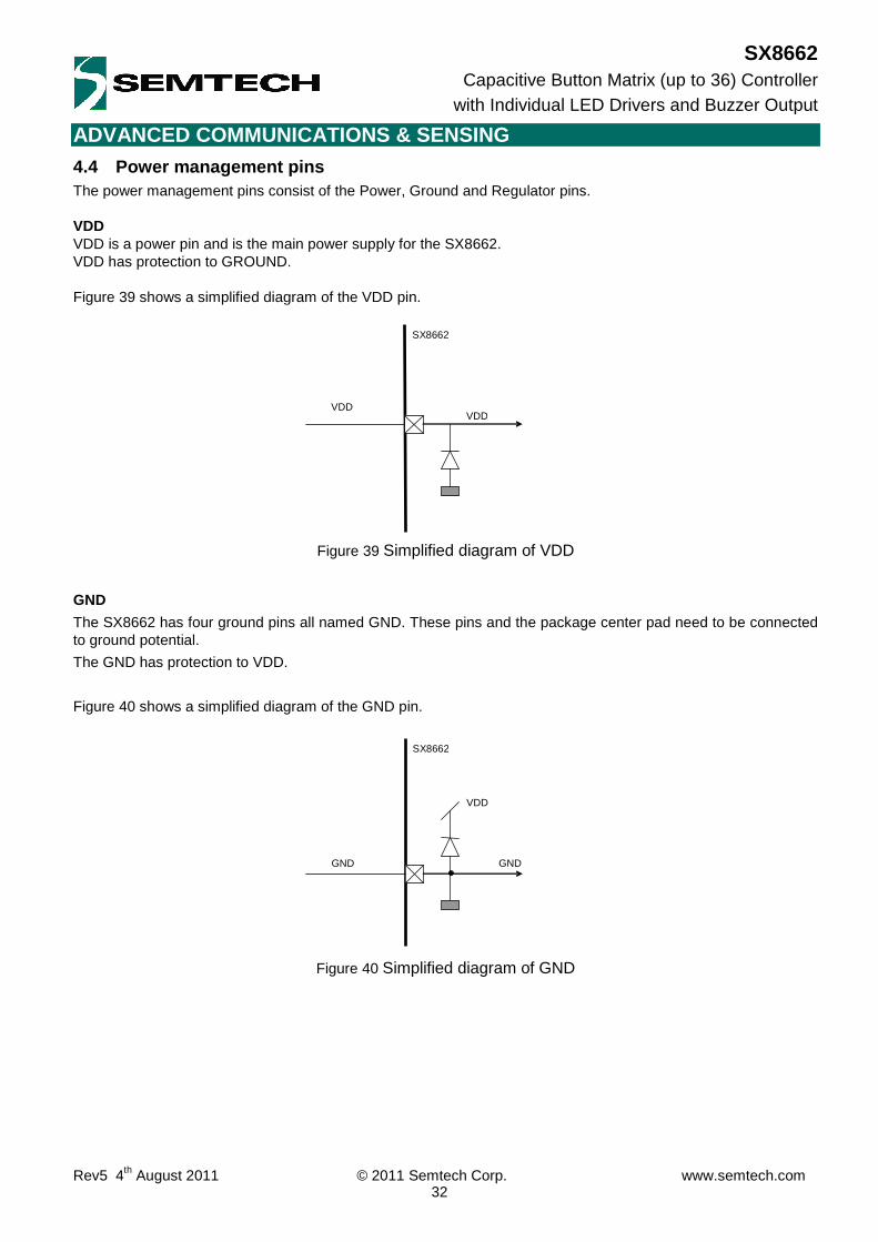
4.4 Power management pins The power management pins consist of the Power, Ground and Regulator pins. VDD VDD is a power pin and is the main power supply for the SX8662. VDD has protection to GROUND. Figure 39 shows a simplified diagram of the VDD pin.
Figure 39 Simplified diagram of VDD
GND
The SX8662 has four ground pins all named GND. These pins and the package center pad need to be connected to ground potential.
The GND has protection to VDD.
Figure 40 shows a simplified diagram of the GND pin.
Figure 40 Simplified diagram of GND
VDD
SX8662
VDD
VDD
SX8662
GND GND

ADVANCED COMMUNICATIONS & SENSING
Rev5 4th August 2011 © 2011 Semtech Corp. www.semtech.com 33
SX8662 Capacitive Button Matrix (up to 36) Controller
with Individual LED Drivers and Buzzer Output
VANA, VDIG
The SX8662 has on-chip regulators for internal use (pins VANA and VDIG). VANA and VDIG have protection to VDD and to GND. The output of the regulators needs to be de-coupled with a small 100nF capacitor to ground. Figure 41 shows a simplified diagram of the VANA and VDIG pin.
Figure 41 Simplified diagram of VANA and VDIG
4.5 General purpose IO pins The SX8662 has 8 General purpose input/output (GPIO) pins. All the GPIO pins have protection to VDD and GND. Figure 42 shows a simplified diagram of the GPIO pins.
Figure 42 Simplified diagram of GPIO pins
VDD SX8662
GND
VDIG
VDD
GND
VANA VANA
VDIG
Cvdig
Cvana

ADVANCED COMMUNICATIONS & SENSING
Rev5 4th August 2011 © 2011 Semtech Corp. www.semtech.com 34
SX8662 Capacitive Button Matrix (up to 36) Controller
with Individual LED Drivers and Buzzer Output
5 DETAILED CONFIGURATION DESCRIPTIONS
5.1 Introduction
The SX8662 configuration parameters are taken from the QSM or the NVM and loaded into the SPM as explained in the chapter ‘functional description’.
This chapter describes the details of the configuration parameters of the SX8662.
The SPM is split by functionality into 5 configuration sections:
• General: operating modes,
• Capacitive Sensors: related to lower level capacitive sensing,
• Buttons (MK and PK): related to the conversion from sensor data towards button information,
• Buzzer: defining parameters for the buzzer
• GPIOs: related to the setup of the GPIO pins.
The total address space of the SPM and the NVM is 128 bytes, from address 0x00 to address 0x7F.
Two types of memory addresses, data are accessible to the user.
• ‘application data’: Application dependent data that need to be configured by the user.
• ‘reserved’: Data that need to be maintained by the user to the QSM default values (i.e. when NVM is burned).
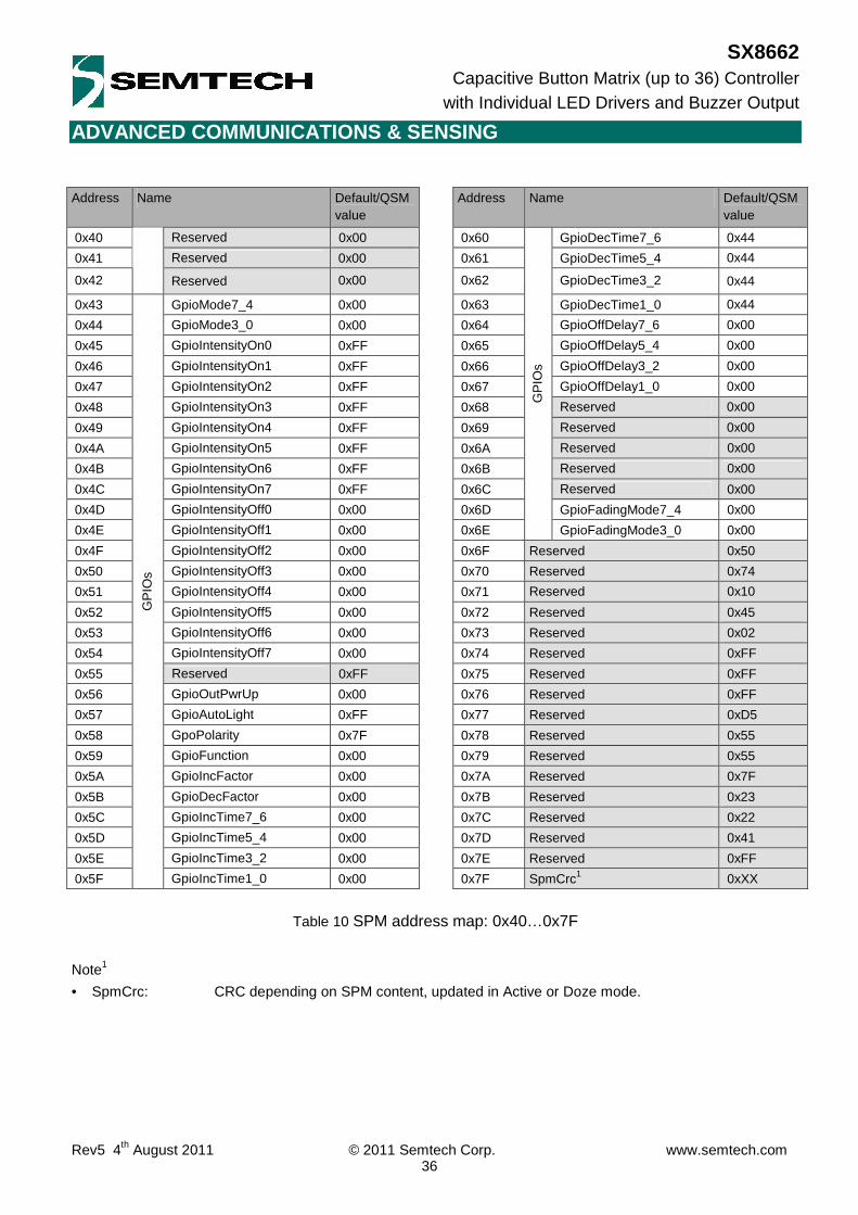
The Table 9 and Table 10 resume the complete SPM address space and show the ‘application data’ and ‘reserved’ addresses, the functional split and the default values (loaded from the QSM).

ADVANCED COMMUNICATIONS & SENSING
Rev5 4th August 2011 © 2011 Semtech Corp. www.semtech.com 35
SX8662 Capacitive Button Matrix (up to 36) Controller
with Individual LED Drivers and Buzzer Output
Address Name Default/QSM value
Address Name Default/QSM value
0x00 Reserved 0xxx 0x20 Reserved 0x00
0x01 Reserved 0xxx 0x21
Reserved 0x00
0x02 Reserved 0x42 0x22 BtnCfg 0x30
0x03 Reserved 0xxx 0x23 BtnAvgThresh 0x50
0x04 I2CAddress 0x2B 0x24 BtnCompNegThresh 0xA0
0x05 ActiveScanPeriod 0x02 0x25 BtnCompNegCntMax 0x01
0x06 DozeScanPeriod 0x0D 0x26 BtnHysteresis 0x0A
0x07 PassiveTimer 0x00 0x27 BtnStuckAtTimeout 0x00
0x08
Gen
eral
Reserved 0x00 0x28 Reserved 0x80
0x09 CapModeMisc 0x00 0x29 Reserved 0x00
0x0A Reserved 0x55 0x2A
But
tons
Reserved 0xFF
0x0B Reserved 0x55 0x2B Reserved 0x00
0x0C Reserved 0x55 0x2C Reserved 0x7D
0x0D CapSensitivity0_1 0x44 0x2D Reserved 0x00
0x0E CapSensitivity2_3 0x44 0x2E Reserved 0x0A
0x0F CapSensitivity4_5 0x44 0x2F Reserved 0x00
0x10 CapSensitivity6_7 0x44 0x30 Reserved 0x64
0x11 CapSensitivity8_9 0x44 0x31 Reserved 0x34
0x12 CapSensitivity10_11 0x44 0x32 Reserved 0x50
0x13 CapThresh0 0xA0 0x33 Reserved 0xA0
0x14 CapThresh1 0xA0 0x34 Reserved 0x01
0x15 CapThresh2 0xA0 0x35 Reserved 0x00
0x16 CapThresh3 0xA0 0x36
Reserved 0x00
0x17 CapThresh4 0xA0 0x37 BuzzerCfg 0xA4
0x18 CapThresh5 0xA0 0x38 BuzzerFreqPhase1 0x40
0x19 CapThresh6 0xA0 0x39 BuzzerFreqPhase2 0x20
0x1A CapThresh7 0xA0 0x3A
Buz
zer
Reserved 0x00
0x1B CapThresh8 0xA0 0x3B Reserved 0x00
0x1C CapThresh9 0xA0 0x3C Reserved 0x00
0x1D CapThresh10 0xA0 0x3D Reserved 0x00
0x1E CapThresh11 0xA0 0x3E Reserved 0x00
0x1F
Cap
aciti
ve S
enso
rs
CapPerComp 0x00 0x3F
Reserved 0x00
Table 9 SPM address map: 0x00…0x3F
Note
• ‘0xxx’: write protected data
ADVANCED COMMUNICATIONS & SENSING
Rev5 4th August 2011 © 2011 Semtech Corp. www.semtech.com 36
SX8662 Capacitive Button Matrix (up to 36) Controller
with Individual LED Drivers and Buzzer Output
Address Name Default/QSM value
Address Name Default/QSM value
0x40 Reserved 0x00 0x60 GpioDecTime7_6 0x44
0x41 Reserved 0x00 0x61 GpioDecTime5_4 0x44
0x42
Reserved 0x00 0x62 GpioDecTime3_2 0x44
0x43 GpioMode7_4 0x00 0x63 GpioDecTime1_0 0x44
0x44 GpioMode3_0 0x00 0x64 GpioOffDelay7_6 0x00
0x45 GpioIntensityOn0 0xFF 0x65 GpioOffDelay5_4 0x00
0x46 GpioIntensityOn1 0xFF 0x66 GpioOffDelay3_2 0x00
0x47 GpioIntensityOn2 0xFF 0x67 GpioOffDelay1_0 0x00
0x48 GpioIntensityOn3 0xFF 0x68 Reserved 0x00
0x49 GpioIntensityOn4 0xFF 0x69 Reserved 0x00
0x4A GpioIntensityOn5 0xFF 0x6A Reserved 0x00
0x4B GpioIntensityOn6 0xFF 0x6B Reserved 0x00
0x4C GpioIntensityOn7 0xFF 0x6C Reserved 0x00
0x4D GpioIntensityOff0 0x00 0x6D GpioFadingMode7_4 0x00
0x4E GpioIntensityOff1 0x00 0x6E G
PIO
s GpioFadingMode3_0 0x00
0x4F GpioIntensityOff2 0x00 0x6F Reserved 0x50
0x50 GpioIntensityOff3 0x00 0x70 Reserved 0x74
0x51 GpioIntensityOff4 0x00 0x71 Reserved 0x10
0x52 GpioIntensityOff5 0x00 0x72 Reserved 0x45
0x53 GpioIntensityOff6 0x00 0x73 Reserved 0x02
0x54 GpioIntensityOff7 0x00 0x74 Reserved 0xFF
0x55 Reserved 0xFF 0x75 Reserved 0xFF
0x56 GpioOutPwrUp 0x00 0x76 Reserved 0xFF
0x57 GpioAutoLight 0xFF 0x77 Reserved 0xD5
0x58 GpoPolarity 0x7F 0x78 Reserved 0x55
0x59 GpioFunction 0x00 0x79 Reserved 0x55
0x5A GpioIncFactor 0x00 0x7A Reserved 0x7F
0x5B GpioDecFactor 0x00 0x7B Reserved 0x23
0x5C GpioIncTime7_6 0x00 0x7C Reserved 0x22
0x5D GpioIncTime5_4 0x00 0x7D Reserved 0x41
0x5E GpioIncTime3_2 0x00 0x7E Reserved 0xFF
0x5F
GP
IOs
GpioIncTime1_0 0x00 0x7F SpmCrc1 0xXX
Table 10 SPM address map: 0x40…0x7F
Note1
• SpmCrc: CRC depending on SPM content, updated in Active or Doze mode.

ADVANCED COMMUNICATIONS & SENSING
Rev5 4th August 2011 © 2011 Semtech Corp. www.semtech.com 37
SX8662 Capacitive Button Matrix (up to 36) Controller
with Individual LED Drivers and Buzzer Output
5.2 General Parameters
General Parameters
Address Name Bits Description
7 Reserved (0) 0x04 I2CAddress
6:0 Defines the I2C address. The I2C address will be active after a reset. Default: 0x2B
0x05 ActiveScanPeriod 7:0 Defines Active Mode Scan Period (Figure 6). 0x00: Reserved 0x01: 15ms 0x02: 30ms (default) … 0xFF: 255 x 15ms
0x06 DozeScanPeriod 7:0 Defines Doze Mode Scan Period (Figure 6). 0x00: Reserved 0x01: 15ms … 0x0D: 195ms (default) … 0xFF: 255 x 15ms
0x07 PassiveTimer 7:0 Defines Passive Timer on Button Information (Figure 7). 0x00: OFF (default) 0x01: 1 second … 0xFF: 255 seconds
0x08 Reserved 7:0 Reserved (0x00)
Table 11 General Parameters

ADVANCED COMMUNICATIONS & SENSING
Rev5 4th August 2011 © 2011 Semtech Corp. www.semtech.com 38
SX8662 Capacitive Button Matrix (up to 36) Controller
with Individual LED Drivers and Buzzer Output
5.3 Capacitive Sensors Parameters Capacitive Sensors Parameters
Address Name Bits Description
7:5 Reserved (000)
4:3 CapSenseProtect: 00: OFF (default) 01: ON. GPIOs activity is disabled during CAP11 sensing. 10: ON. GPIOs activity is disabled during CAP10-11 sensing. 11: ON. GPIOs activity is disabled during CAP0-11 sensing (i.e. all CAPx).
0x09 CapModeMisc
2:0 IndividualSensitivity Defines common sensitivity for all sensors or individual sensor sensitivity. 000: Common sensitivity settings (CapSensitivity0_1[7:4]) (default) 100: Individual sensitivity settings (CapSensitivityx_x) Else : Reserved
0x0A Reserved 7:0 Reserved (0x55)
0x0B Reserved 7:0 Reserved (0x55)
0x0C Reserved 7:0 Reserved (0x55)
7:4 CAP0 Sensitivity - Common Sensitivity 0x0D CapSensitivity0_1
3:0 CAP1 Sensitivity
7:4 CAP2 Sensitivity 0x0E CapSensitivity2_3
3:0 CAP3 Sensitivity
7:4 CAP4 Sensitivity 0x0F CapSensitivity4_5
3:0 CAP5 Sensitivity
7:4 CAP6 Sensitivity 0x10 CapSensitivity6_7
3:0 CAP7 Sensitivity
7:4 CAP8 Sensitivity 0x11 CapSensitivity8_9
3:0 CAP9 Sensitivity
7:4 CAP10 Sensitivity 0x12 CapSensitivity10_11
3:0 CAP11 Sensitivity
Defines the sensitivity. 0x0: Minimum 0x1: 1 … 0x4: 4 (default) … 0x7: Maximum 0x8..0xF: Reserved
0x13 CapThresh0 7:0 CAP0 Touch Threshold
0x14 CapThresh1 7:0 CAP1 Touch Threshold
0x15 CapThresh2 7:0 CAP2 Touch Threshold
0x16 CapThresh3 7:0 CAP3 Touch Threshold
0x17 CapThresh4 7:0 CAP4 Touch Threshold
0x18 CapThresh5 7:0 CAP5 Touch Threshold
0x19 CapThresh6 7:0 CAP6 Touch Threshold
0x1A CapThresh7 7:0 CAP7 Touch Threshold
0x1B CapThresh8 7:0 CAP8 Touch Threshold
0x1C CapThresh9 7:0 CAP9 Touch Threshold
0x1D CapThresh10 7:0 CAP10 Touch Threshold
0x1E CapThresh11 7:0 CAP11 Touch Threshold
Defines the Touch Threshold ticks. 0x00: 0, 0x01: 4, … 0xA0: 640 (default), … 0xFF: 1020
0x1F CapPerComp 7:4 Reserved (0000)

ADVANCED COMMUNICATIONS & SENSING
Rev5 4th August 2011 © 2011 Semtech Corp. www.semtech.com 39
SX8662 Capacitive Button Matrix (up to 36) Controller
with Individual LED Drivers and Buzzer Output
Capacitive Sensors Parameters
Address Name Bits Description
3:0 Periodic Offset Compensation Defines the periodic offset compensation. 0x0: OFF (default) 0x1: 1 second 0x2: 2 seconds … 0x7: 7 seconds 0x8: 16 seconds 0x9: 18 seconds … 0xE: 28 seconds 0xF: 60 seconds
Table 12 Capacitive Sensors Parameters
CapSenseProtect
If needed, ASI activity can be protected against LED interference by automatically disabling GPIOs during sensing periods. At the end of the sensing activity, GPIOs activity resume normally.
CapModeMisc
By default the ASI uses common sensitivity for all capacitive sensors in the case overlay material and sensors sizes are about equal. The register bits CapSensitivity0_1[7:4] determine the sensitivity for all sensors in common sensitivity mode. The ASI can use an individual sensitivity for each CAP pin The individual sensitivity mode results in longer sensing periods than required in common sensitivity mode.
CapSensitivity0_1, CapSensitivity2_3, CapSensitivity4_5, CapSensitivity6_7, CapSensitivity8_9, CapSensitivity10_11
The sensitivity of the sensors can be set between 8 values. The higher the sensitivity is set the larger the value of the ticks will be. The minimum sensitivity can be used for thin overlay materials and large sensors, while the maximum sensitivity is required for thicker overlay and smaller sensors. The required sensitivity needs to be determined during a product development phase. Too low sensitivity settings result in missing touches. Too high sensitivity settings will result in fault detection of fingers hovering above the touch sensors. The sensitivity is identical for all sensors in common sensitivity mode using the bits CapSensitivity0_1[7:4] and can be set individually using register CapModeMisc[2:0].
CapThresh0, CapThresh1, CapThresh2, CapThresh3, CapThresh4, CapThresh5, CapThresh6, CapThresh7, CapThresh8, CapThresh9, CapThresh10, CapThresh11:
For each CAP pin a threshold level can be set individually. The threshold levels are used by the SX8662 for making touch and release decisions. The details are explained in the sections for buttons.
CapPerComp
The SX8662 offers a periodic offset compensation for applications which are subject to substantial environmental changes. The periodic offset compensation is done at a defined interval and only if buttons are released.
ADVANCED COMMUNICATIONS & SENSING
Rev5 4th August 2011 © 2011 Semtech Corp. www.semtech.com 40
SX8662 Capacitive Button Matrix (up to 36) Controller
with Individual LED Drivers and Buzzer Output
5.4 Buttons (MK and PK) Parameters
Buttons Parameters
Address Name Bits Description
7 Reporting scheme: 0: report both MK and PK touches (multi MK touch is never allowed/reported) (default) 1: report first/single MK or PK touch (ignore next touch until release of the first one)
6 Priority key (PK): 0: OFF (default) 1: ON (CAP11)
5:4 Button events to be reported on NIRQ. 00 : None 01 : Touch 10 : Release 11 : Both (default)
3:2 Defines the number of samples at the scan period for determining a release of a button. 00 : no debounce, use incoming sample (default) 01 : 2 samples debounce 10 : 3 samples debounce 11 : 4 samples debounce
0x22 BtnCfg
1:0 Defines the number of samples at the scan period for determining a touch of a button. 00 : no debounce, use incoming sample (default) 01 : 2 samples debounce 10 : 3 samples debounce 11 : 4 samples debounce
0x23 BtnAvgThresh 7:0 Defines the positive threshold for disabling the processing filter averaging. If ticks are above the threshold, then the averaging is suspended. 0x00: 0 0x01: 4 … 0x50: 320 (default) … 0xFF: 1020
0x24 BtnCompNegThresh 7:0 Defines the negative offset compensation threshold. 0x00: 0 0x01: 4 … 0xA0: 640 (default) … 0xFF: 1020
0x25 BtnCompNegCntMax 7:0 Defines the number of ticks (below the negative offset compensation threshold) which will initiate an offset compensation. 0x00: reserved 0x01: 1 sample (default) … 0xFF: 255 samples
0x26 BtnHysteresis 7:0 Defines the button hysteresis corresponding to a percentage of the CAP thresholds (defined in Table 12). All buttons use the same hysteresis. 0x00: 0% 0x01: 1% … 0x0A: 10% (default) …
ADVANCED COMMUNICATIONS & SENSING
Rev5 4th August 2011 © 2011 Semtech Corp. www.semtech.com 41
SX8662 Capacitive Button Matrix (up to 36) Controller
with Individual LED Drivers and Buzzer Output
Buttons Parameters
Address Name Bits Description
0x64: 100%
0x27 BtnStuckAtTimeout 7:0 Defines the stuck at timeout for buttons. 0x00: OFF (default) 0x01: 1 second … 0xFF: 255 seconds
Table 13 Button Parameters
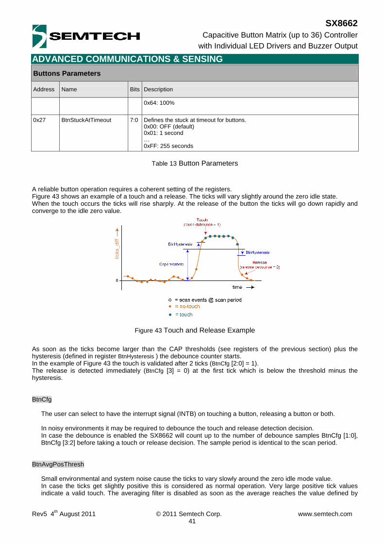
A reliable button operation requires a coherent setting of the registers. Figure 43 shows an example of a touch and a release. The ticks will vary slightly around the zero idle state. When the touch occurs the ticks will rise sharply. At the release of the button the ticks will go down rapidly and converge to the idle zero value.
ticks_diff
Figure 43 Touch and Release Example
As soon as the ticks become larger than the CAP thresholds (see registers of the previous section) plus the hysteresis (defined in register BtnHysteresis ) the debounce counter starts. In the example of Figure 43 the touch is validated after 2 ticks (BtnCfg [2:0] = 1). The release is detected immediately (BtnCfg [3] = 0) at the first tick which is below the threshold minus the hysteresis. BtnCfg
The user can select to have the interrupt signal (INTB) on touching a button, releasing a button or both. In noisy environments it may be required to debounce the touch and release detection decision. In case the debounce is enabled the SX8662 will count up to the number of debounce samples BtnCfg [1:0], BtnCfg [3:2] before taking a touch or release decision. The sample period is identical to the scan period.
BtnAvgPosThresh
Small environmental and system noise cause the ticks to vary slowly around the zero idle mode value. In case the ticks get slightly positive this is considered as normal operation. Very large positive tick values indicate a valid touch. The averaging filter is disabled as soon as the average reaches the value defined by

ADVANCED COMMUNICATIONS & SENSING
Rev5 4th August 2011 © 2011 Semtech Corp. www.semtech.com 42
SX8662 Capacitive Button Matrix (up to 36) Controller
with Individual LED Drivers and Buzzer Output
BtnAvgPosThresh. This mechanism avoids that a valid touch will be averaged and finally the tick difference becomes zero. In case three or more sensors reach the BtnAvgPosThresh value simultaneously then the SX8662 will start an offset compensation procedure.
Small environmental and system noise cause the ticks to vary slowly around the zero idle mode value. In case the ticks get slightly negative this is considered as normal operation. However large negative values will trigger an offset compensation phase and a new set of DCVs will be obtained. The decision to trigger a compensation phase based on negative ticks is determined by the value in the register BtnCompNegThresh and by the number of ticks below the negative thresholds defined in register BtnCompNegCntMax. An example is shown in Figure 44.
ticks_avg
Figure 44 Negative Ticks Offset Compensation Trigger
BtnCompNegThresh
Small negative ticks are considered as normal operation and will occur very often. Larger negative ticks however need to be avoided and a convenient method is to trigger an offset compensation phase. The new set of DCV will assure the idle ticks will be close to zero again. A trade-off has to be found for the value of this register. A negative threshold too close to zero will trigger a compensation phase very often. A very negative threshold will never trigger.
BtnCompNegCntMax As soon as the ticks get smaller than the Negative Threshold the Negative Counter starts to count. If the counter goes beyond the Negative Counter Max then the offset compensation phase is triggered. The recommended value for this register is ‘1’ which means that the offset compensation starts on the first tick below the negative threshold.
BtnHysteresis The hysteresis percentage is identical for all buttons. A touch is detected if the ticks are getting larger as the value defined by:
CapThreshold + CapThreshold * hysteresis. A release is detected if the ticks are getting smaller as the value defined by:
CapThreshold - CapThreshold * hysteresis.
BtnStuckAtTimeout The stuckat timer can avoid sticky buttons. If the stuckat timer is set to one second then the touch of a finger will last only for one second and then a compensation will be performed and button hence considered released, even if the finger remains on the button for a longer time. After the actual finger release the button can be touched again and will be reported as usual. In case the stuckat timer is not required it can be set to zero.

ADVANCED COMMUNICATIONS & SENSING
Rev5 4th August 2011 © 2011 Semtech Corp. www.semtech.com 43
SX8662 Capacitive Button Matrix (up to 36) Controller
with Individual LED Drivers and Buzzer Output
5.5 Buzzer Parameters
Buzzer Parameters
Address Name Bits Description
7:6 Defines the phase 1 duration. 0x00: ~ 5ms 0x01: ~ 10ms 0x02: ~ 15ms (default) 0x03: ~ 30ms
5:4 Defines the phase 2 duration. 0x00: ~ 5ms 0x01: ~ 10ms 0x02: ~ 15ms (default) 0x03: ~ 30ms
3 Defines the buzzer idle level (BuzzerLevelIdle). 0x0: min level (0V), (default) 0x1: max level (VDD)
0x37 BuzzerCfg
2:0 Defines the buzzer pwm prescaler value. Default: 0x04
0x38 BuzzerFreqPhase1 7:0 Defines the frequency for the first phase of the buzzer. freq ≈ 4MHz /(2^prescaler * BuzzerFreqPhase1) Default: 0x40 (4KHz)
0x39 BuzzerFreqPhase2 7:0 Defines the frequency for the second phase of the buzzer. freq ≈ 4MHz /(2^prescaler * BuzzerFreqPhase2) Default: 0x20 (8KHz)
0x3A Reserved 7:0 Reserved (0x00)
Table 14 Buzzer Parameters
The SX8662 has the ability to drive a buzzer (on GPIO7) to provide an audible indication that a button has been touched. The buzzer is driven by a square signal for approximately 30ms (default). During the first phase (15ms) the signal’s frequency is default 4KHz while in the second phase (15ms) the signal’s frequency default is 8KHz. The buzzer is activated only once during any button touch and is not repeated for long touches. The user can choose to enable or disable the buzzer by configuration and define the idle level, frequencies and phase durations.
Figure 45 Buzzer behavior
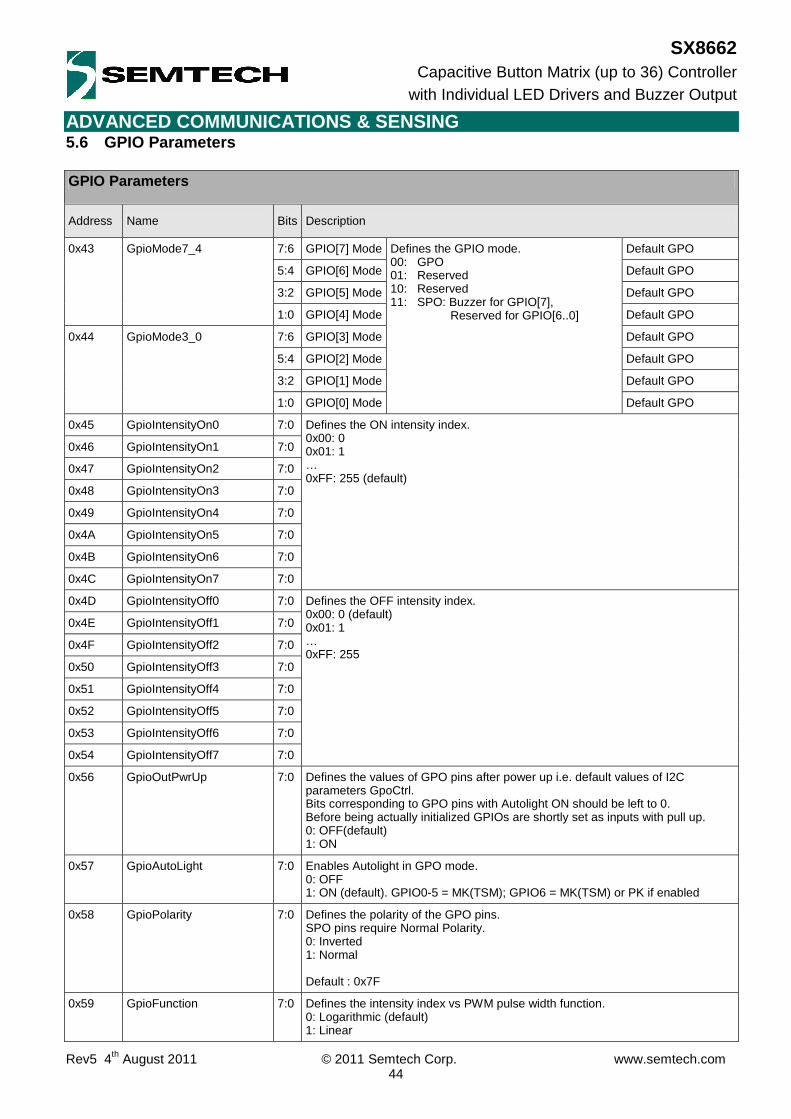
ADVANCED COMMUNICATIONS & SENSING
Rev5 4th August 2011 © 2011 Semtech Corp. www.semtech.com 44
SX8662 Capacitive Button Matrix (up to 36) Controller
with Individual LED Drivers and Buzzer Output
5.6 GPIO Parameters GPIO Parameters
Address Name Bits Description
7:6 GPIO[7] Mode Default GPO
5:4 GPIO[6] Mode Default GPO
3:2 GPIO[5] Mode Default GPO
0x43 GpioMode7_4
1:0 GPIO[4] Mode Default GPO
7:6 GPIO[3] Mode Default GPO
5:4 GPIO[2] Mode Default GPO
3:2 GPIO[1] Mode Default GPO
0x44 GpioMode3_0
1:0 GPIO[0] Mode
Defines the GPIO mode. 00: GPO 01: Reserved 10: Reserved 11: SPO: Buzzer for GPIO[7], Reserved for GPIO[6..0]
Default GPO
0x45 GpioIntensityOn0 7:0
0x46 GpioIntensityOn1 7:0
0x47 GpioIntensityOn2 7:0
0x48 GpioIntensityOn3 7:0
0x49 GpioIntensityOn4 7:0
0x4A GpioIntensityOn5 7:0
0x4B GpioIntensityOn6 7:0
0x4C GpioIntensityOn7 7:0
Defines the ON intensity index. 0x00: 0 0x01: 1 … 0xFF: 255 (default)
0x4D GpioIntensityOff0 7:0
0x4E GpioIntensityOff1 7:0
0x4F GpioIntensityOff2 7:0
0x50 GpioIntensityOff3 7:0
0x51 GpioIntensityOff4 7:0
0x52 GpioIntensityOff5 7:0
0x53 GpioIntensityOff6 7:0
0x54 GpioIntensityOff7 7:0
Defines the OFF intensity index. 0x00: 0 (default) 0x01: 1 … 0xFF: 255
0x56 GpioOutPwrUp 7:0 Defines the values of GPO pins after power up i.e. default values of I2C parameters GpoCtrl. Bits corresponding to GPO pins with Autolight ON should be left to 0. Before being actually initialized GPIOs are shortly set as inputs with pull up. 0: OFF(default) 1: ON
0x57 GpioAutoLight 7:0 Enables Autolight in GPO mode. 0: OFF 1: ON (default). GPIO0-5 = MK(TSM); GPIO6 = MK(TSM) or PK if enabled
0x58 GpioPolarity 7:0 Defines the polarity of the GPO pins. SPO pins require Normal Polarity. 0: Inverted 1: Normal Default : 0x7F
0x59 GpioFunction 7:0 Defines the intensity index vs PWM pulse width function. 0: Logarithmic (default) 1: Linear

ADVANCED COMMUNICATIONS & SENSING
Rev5 4th August 2011 © 2011 Semtech Corp. www.semtech.com 45
SX8662 Capacitive Button Matrix (up to 36) Controller
with Individual LED Drivers and Buzzer Output
GPIO Parameters
Address Name Bits Description
0x5A GpioIncFactor 7:0 Defines the fading increment factor. 0: intensity index incremented every increment time (default) 1: intensity index incremented every 16 increment times
0x5B GpioDecFactor 7:0 Defines the fading decrement factor. 0: intensity index decremented every decrement time (default) 1: intensity index decremented every 16 decrement times
7:4 GPIO[7] Fading Increment Time 0x5C GpioIncTime7_6
3:0 GPIO[6] Fading Increment Time
7:4 GPIO[5] Fading Increment Time 0x5D GpioIncTime5_4
3:0 GPIO[4] Fading Increment Time
7:4 GPIO[3] Fading Increment Time 0x5E GpioIncTime3_2
3:0 GPIO[2] Fading Increment Time
7:4 GPIO[1] Fading Increment Time 0x5F GpioIncTime1_0
3:0 GPIO[0] Fading Increment Time
Defines the fading increment time. 0x0: OFF (default) 0x1: 0.5ms 0x2: 1ms … 0xF: 7.5ms The total fading in time will be: GpioIncTime*GpioIncFactor* (GpioIntensityOn – GpioIntensityOff)
7:4 GPIO[7] Fading Decrement Time 0x60 GpioDecTime7_6
3:0 GPIO[6] Fading Decrement Time
7:4 GPIO[5] Fading Decrement Time 0x61 GpioDecTime5_4
3:0 GPIO[4] Fading Decrement Time
7:4 GPIO[3] Fading Decrement Time 0x62 GpioDecTime3_2
3:0 GPIO[2] Fading Decrement Time
7:4 GPIO[1] Fading Decrement Time 0x63 GpioDecTime1_0
3:0 GPIO[0] Fading Decrement Time
Defines the fading decrement time. 0x0: OFF 0x1: 0.5ms 0x2: 1ms … 0x4: 2.0ms (default) … 0xF: 7.5ms The total fading out time will be: GpioDecTime*GpioDecFactor* (GpioIntensityOn – GpioIntensityOff)
7:4 GPIO[7] OFF Delay 0x64 GpioOffDelay7_6
3:0 GPIO[6] OFF Delay
7:4 GPIO[5] OFF Delay 0x65 GpioOffDelay5_4
3:0 GPIO[4] OFF Delay
7:4 GPIO[3] OFF Delay 0x66 GpioOffDelay3_2
3:0 GPIO[2] OFF Delay
7:4 GPIO[1] OFF Delay 0x67 GpioOffDelay1_0
3:0 GPIO[0] OFF Delay
Defines the delay between release and start of fading out (single fading) 0x0: instantaneous (default) 0x1: 200 ms 0x2: 400 ms 0x3: 600ms … 0xA: 2s 0xB: 4s … 0xF: 12s
0x68 Reserved 7:0 Reserved (0x00)
0x69 Reserved 7:0 Reserved (0x00)
0x6A Reserved 7:0 Reserved (0x00)
0x6B Reserved 7:0 Reserved (0x00)
0x6C Reserved 7:0 Reserved (0x00)
7:6 Fading mode for GPIO[7]
5:4 Fading mode for GPIO[6]
3:2 Fading mode for GPIO[5]
0x6D GpioFadingMode7_4
1:0 Fading mode for GPIO[4]
0x6E GpioFadingMode3_0 7:6 Fading mode for GPIO[3]
Defines the Fading mode for GPO[7:0]. 00: Single (default) 01: Continuous 10: Reserved 11: Reserved

ADVANCED COMMUNICATIONS & SENSING
Rev5 4th August 2011 © 2011 Semtech Corp. www.semtech.com 46
SX8662 Capacitive Button Matrix (up to 36) Controller
with Individual LED Drivers and Buzzer Output
GPIO Parameters
Address Name Bits Description
5:4 Fading mode for GPIO[2]
3:2 Fading mode for GPIO[1]
1:0 Fading mode for GPIO[0]
The fading modes are expected to be defined at power up by the QSM or NVM. In case the fading modes need to be changed after power up this can be done when the GPOs are all OFF.
Table 15 resumes the applicable SPM and I2C parameters for each GPIO mode.
GPO Autolight OFF
GPO Autolight ON
SPO (Buzzer – GPIO7 only)
GpioMode X X X GpioOutPwrUp X1 OFF OFF GpioAutolight OFF ON ON
GpioPolarity X TSM->Normal else X Normal
GpioIntensityOn X X
GpioIntensityOff X TSM->0% else X
GpioFunction X X Linear GpioIncFactor X X GpioDecFactor X X GpioIncTime X X GpioDecTime X X GpioOffDelay X X
SPM
GpioFadingMode X X I2C GpoCtrl X
1 GpioOutPwrUp must be set to OFF in Continuous Fading Mode
Grey = not applicable, with or without required setting
Table 15 Applicable (X) SPM/I2C Parameters vs. GPIO Mode
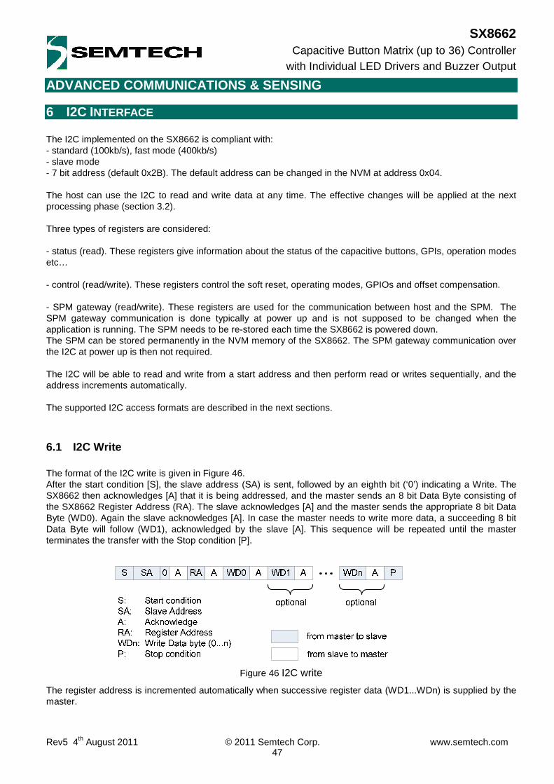
ADVANCED COMMUNICATIONS & SENSING
Rev5 4th August 2011 © 2011 Semtech Corp. www.semtech.com 47
SX8662 Capacitive Button Matrix (up to 36) Controller
with Individual LED Drivers and Buzzer Output
6 I2C INTERFACE The I2C implemented on the SX8662 is compliant with: - standard (100kb/s), fast mode (400kb/s) - slave mode - 7 bit address (default 0x2B). The default address can be changed in the NVM at address 0x04. The host can use the I2C to read and write data at any time. The effective changes will be applied at the next processing phase (section 3.2). Three types of registers are considered: - status (read). These registers give information about the status of the capacitive buttons, GPIs, operation modes etc… - control (read/write). These registers control the soft reset, operating modes, GPIOs and offset compensation. - SPM gateway (read/write). These registers are used for the communication between host and the SPM. The SPM gateway communication is done typically at power up and is not supposed to be changed when the application is running. The SPM needs to be re-stored each time the SX8662 is powered down. The SPM can be stored permanently in the NVM memory of the SX8662. The SPM gateway communication over the I2C at power up is then not required. The I2C will be able to read and write from a start address and then perform read or writes sequentially, and the address increments automatically. The supported I2C access formats are described in the next sections.
6.1 I2C Write The format of the I2C write is given in Figure 46. After the start condition [S], the slave address (SA) is sent, followed by an eighth bit (‘0’) indicating a Write. The SX8662 then acknowledges [A] that it is being addressed, and the master sends an 8 bit Data Byte consisting of the SX8662 Register Address (RA). The slave acknowledges [A] and the master sends the appropriate 8 bit Data Byte (WD0). Again the slave acknowledges [A]. In case the master needs to write more data, a succeeding 8 bit Data Byte will follow (WD1), acknowledged by the slave [A]. This sequence will be repeated until the master terminates the transfer with the Stop condition [P].
Figure 46 I2C write
The register address is incremented automatically when successive register data (WD1...WDn) is supplied by the master.
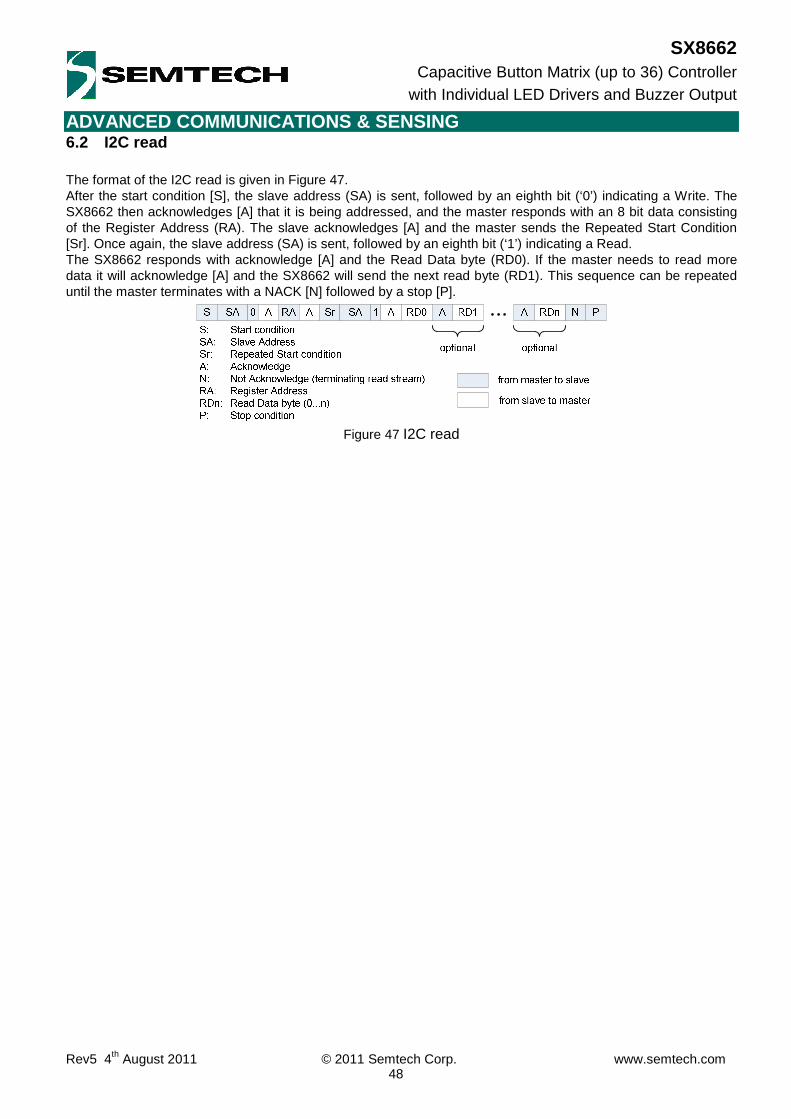
ADVANCED COMMUNICATIONS & SENSING
Rev5 4th August 2011 © 2011 Semtech Corp. www.semtech.com 48
SX8662 Capacitive Button Matrix (up to 36) Controller
with Individual LED Drivers and Buzzer Output
6.2 I2C read The format of the I2C read is given in Figure 47. After the start condition [S], the slave address (SA) is sent, followed by an eighth bit (‘0’) indicating a Write. The SX8662 then acknowledges [A] that it is being addressed, and the master responds with an 8 bit data consisting of the Register Address (RA). The slave acknowledges [A] and the master sends the Repeated Start Condition [Sr]. Once again, the slave address (SA) is sent, followed by an eighth bit (‘1’) indicating a Read. The SX8662 responds with acknowledge [A] and the Read Data byte (RD0). If the master needs to read more data it will acknowledge [A] and the SX8662 will send the next read byte (RD1). This sequence can be repeated until the master terminates with a NACK [N] followed by a stop [P].
Figure 47 I2C read
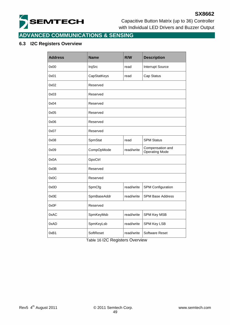
ADVANCED COMMUNICATIONS & SENSING
Rev5 4th August 2011 © 2011 Semtech Corp. www.semtech.com 49
SX8662 Capacitive Button Matrix (up to 36) Controller
with Individual LED Drivers and Buzzer Output
6.3 I2C Registers Overview
Address Name R/W Description
0x00 IrqSrc read Interrupt Source
0x01 CapStatKeys read Cap Status
0x02 Reserved
0x03 Reserved
0x04 Reserved
0x05 Reserved
0x06 Reserved
0x07 Reserved
0x08 SpmStat read SPM Status
0x09 CompOpMode read/write Compensation and Operating Mode
0x0A GpoCtrl
0x0B Reserved
0x0C Reserved
0x0D SpmCfg read/write SPM Configuration
0x0E SpmBaseAddr read/write SPM Base Address
0x0F Reserved
0xAC SpmKeyMsb read/write SPM Key MSB
0xAD SpmKeyLsb read/write SPM Key LSB
0xB1 SoftReset read/write Software Reset
Table 16 I2C Registers Overview

ADVANCED COMMUNICATIONS & SENSING
Rev5 4th August 2011 © 2011 Semtech Corp. www.semtech.com 50
SX8662 Capacitive Button Matrix (up to 36) Controller
with Individual LED Drivers and Buzzer Output
6.4 Status Registers
Address Name Bits Description
7 Reserved
6 NVM burn interrupt flag
5 SPM write interrupt flag
4 Reserved
3 Reserved
2 Sensors interrupt flag
1 Compensation interrupt flag
0x00 IrqSrc
0 Operating Mode interrupt flag
Interrupt source flags 0: Inactive (default) 1: Active INTB goes low if any of these bits is set. More than one bit can be set. Reading IrqSrc clears it together with INTB.
Table 17 Interrupt Source
The delay between the actual event and the flags indicating the interrupt source may be one scan period. IrqSrc[6] is set once NVM burn procedure is completed.
IrqSrc[5] is set once SPM write is effective.
IrqSrc[2] is set if a sensor event occurred. CapStatKeys show the detailed status of the sensors.
IrqSrc[1] is set once compensation procedure is completed either through automatic trigger or via host request.
IrqSrc[0] is set when actually entering Active or Doze mode via host request. CompOpmode shows the current operation mode.

ADVANCED COMMUNICATIONS & SENSING
Rev5 4th August 2011 © 2011 Semtech Corp. www.semtech.com 51
SX8662 Capacitive Button Matrix (up to 36) Controller
with Individual LED Drivers and Buzzer Output
Address Name Bits Description
7 Reserved
6 Priority Key Status 0 : not touched. 1 : touched.
0x01 CapStatKeys
5:0
Matrix Keys Status 0x00: no touch on matrix 0x01: key1 (MK1) is touched 0x02: key2 (MK2) is touched … 0x24: key36 (MK36) is touched If several matrix buttons are touched only the first one is reported. Cf figure below for MK mapping/numbering vs CAPx pins
Table 18 I2C Cap status
Figure 48 Matrix Keys Mapping
Address Name Bits Description
7:4 reserved 0x08 SpmStat
3 NvmValid Indicates if the current NVM is valid. 0: No – QSM is used 1: Yes – NVM is used
ADVANCED COMMUNICATIONS & SENSING
Rev5 4th August 2011 © 2011 Semtech Corp. www.semtech.com 52
SX8662 Capacitive Button Matrix (up to 36) Controller
with Individual LED Drivers and Buzzer Output
Address Name Bits Description
2:0 NvmCount
Indicates the number of times NVM has been burned: 0: None – QSM is used (default) 1: Once – NVM is used if NvmValid = 1, else QSM. 2: Twice – NVM is used if NvmValid = 1, else QSM. 3: Three times – NVM is used if NvmValid = 1, else QSM. 4: More than three times – QSM is used
Table 19 I2C SPM status
6.5 Control Registers
Address Name Bits Description
7:3 Reserved*, write only ‘00000’
2 Compensation
Indicates/triggers compensation procedure 0: Compensation completed (default) 1: read -> compensation running ; write -> trigger compensation 0x09 CompOpMode
1:0 Operating Mode
Indicates/programs** operating mode 00: Active mode (default) 01: Doze mode 10: Sleep mode 11: Reserved
* The reading of these reserved bits will return varying values. ** After the operating mode change (Active/Doze) the host should wait for INTB or 300ms before
performing any I2C read access. Table 20 I2C compensation, operation modes
Address Name Bits Description
0x0A GpoCtrl 7:0 GpoCtrl[7:0]
Triggers ON/OFF state of GPOs when Autolight is OFF 0: OFF (i.e. go to IntensityOff) 1: ON (i.e. go to IntensityOn) Default is set by SPM parameter GpioOutPwrUp Bits of non-GPO pins are ignored.
Table 21 I2C GPO Control
Address Name Bits Description
0xB1 SoftReset 7:0 Writing 0xDE followed by 0x00 will reset the chip.
Table 22 I2C Soft Reset
ADVANCED COMMUNICATIONS & SENSING
Rev5 4th August 2011 © 2011 Semtech Corp. www.semtech.com 53
SX8662 Capacitive Button Matrix (up to 36) Controller
with Individual LED Drivers and Buzzer Output
6.6 SPM Gateway Registers The SX8662 I2C interface offers two registers for exchanging the SPM data with the host. • SpmCfg • SpmBaseAddr
Address Name Bits Description
7:6 00: Reserved
5:4
Defines the normal operation or SPM mode 00: I2C in normal operation mode (default) 01: I2C in SPM mode 10: Reserved 11: Reserved
3 Defines r/w direction of SPM 0: SPM write access (default) 1: SPM read access
0x0D SpmCfg
2:0 000: Reserved
Table 23 SPM access configuration
Address Name Bits Description
0x0E SpmBaseAddr 7:0 SPM Base Address (modulo 8). The lowest address is 0x00 (default) The highest address is 0x78.
Table 24 SPM Base Address
The exchange of data, read and write, between the host and the SPM is always done in bursts of eight bytes. The base address of each burst of eight bytes is a modulo 8 number, starting at 0x00 and ending at 0x78. The registers SpmKeyMsb and SpmKeyLsb are required for NVM programming as described in section 6.7.
Address Name Bits Description
0xAC SpmKeyMsb 7:0 SPM to NVM burn Key MSB Unlock requires writing data: 0x62
Table 25 SPM Key MSB at I2C register address 0xAC
Address Name Bits Description
0xAD SpmKeyLsb 7:0 SPM to NVM burn Key LSB Unlock requires writing data: 0x9D
Table 26 SPM Key LSB
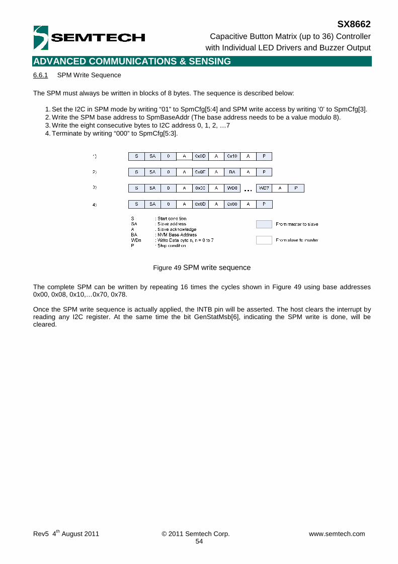
ADVANCED COMMUNICATIONS & SENSING
Rev5 4th August 2011 © 2011 Semtech Corp. www.semtech.com 54
SX8662 Capacitive Button Matrix (up to 36) Controller
with Individual LED Drivers and Buzzer Output
6.6.1 SPM Write Sequence
The SPM must always be written in blocks of 8 bytes. The sequence is described below:
1. Set the I2C in SPM mode by writing “01” to SpmCfg[5:4] and SPM write access by writing ‘0’ to SpmCfg[3]. 2. Write the SPM base address to SpmBaseAddr (The base address needs to be a value modulo 8). 3. Write the eight consecutive bytes to I2C address 0, 1, 2, …7 4. Terminate by writing “000” to SpmCfg[5:3].
Figure 49 SPM write sequence
The complete SPM can be written by repeating 16 times the cycles shown in Figure 49 using base addresses 0x00, 0x08, 0x10,…0x70, 0x78. Once the SPM write sequence is actually applied, the INTB pin will be asserted. The host clears the interrupt by reading any I2C register. At the same time the bit GenStatMsb[6], indicating the SPM write is done, will be cleared.

ADVANCED COMMUNICATIONS & SENSING
Rev5 4th August 2011 © 2011 Semtech Corp. www.semtech.com 55
SX8662 Capacitive Button Matrix (up to 36) Controller
with Individual LED Drivers and Buzzer Output
6.6.2 SPM Read Sequence
The SPM must always be read in blocks of 8 bytes. The sequence is described below:
1. Set the I2C in SPM mode by writing “01” to SpmCfg[5:4] and SPM read access by writing ‘1’ to SpmCfg[3]. 2. Write the SPM base address to SpmBaseAddr (The base address needs to be a value modulo 8). 3. Read the eight consecutive bytes from I2C address 0, 1, 2, …7 4. Terminate by writing “000” to SpmCfg[5:3].
Figure 50 SPM Read Sequence
The complete SPM can be read by repeating 16 times the cycles shown in Figure 50 using base addresses 0x00, 0x08, 0x10,…0x70, 0x78. Once the SPM read sequence is actually applied, the INTB pin will be asserted. The host clears the interrupt by reading any I2C register. At the same time the bit GenStatMsb[6], indicating the SPM write is done, will be cleared.

ADVANCED COMMUNICATIONS & SENSING
Rev5 4th August 2011 © 2011 Semtech Corp. www.semtech.com 56
SX8662 Capacitive Button Matrix (up to 36) Controller
with Individual LED Drivers and Buzzer Output
6.7 NVM burn The content of the SPM can be copied permanently (burned) into the NVM to be used as the new default parameters. The burning of the NVM can be done up to three times and must be done only when the SPM is completely written with the desired data. The number of times the NVM has been burned can be monitored by reading NvmCycle from the I2C register GenStatLsb[7:5].
Figure 51 Simplified Diagram NvmCycle
Figure 51 shows the simplified diagram of the NvmCycle counter. The SX8662 is delivered with empty NVM and NvmCycle set to zero. The SPM points to the QSM. Each NVM burn will increase the NvmCycle. At the fourth NVM burn the SX8662 switches definitely to the QSM. The burning of the SPM into the NVM is done by executing a special sequence of four I2C commands.
1. Write the data 0x62 to the I2C register I2CKeyMsb. Terminate the I2C write by a STOP. 2. Write the data 0x9D to the I2C register I2CKeyLsb. Terminate the I2C write by a STOP. 3. Write the data 0xA5 to the I2C register I2CSpmBaseAddr. Terminate the I2C write by a STOP. 4. Write the data 0x5A to the I2C register I2CSpmBaseAddr. Terminate the I2C write by a STOP.
This is illustrated in Figure 52.
S SA 0 0x0EA 0xA5A PA
S : Start condition
SA : Slave address
A : Slave acknowledge
P : Stop condition
From master to slave
From slave to master
S SA 0 0x0EA 0x5AA PA
3)
4)
S SA 0 0xACA 0x62A PA
S SA 0 0xADA 0x9DA PA
1)
2)
Figure 52: NVM burn procedure

ADVANCED COMMUNICATIONS & SENSING
Rev5 4th August 2011 © 2011 Semtech Corp. www.semtech.com 57
SX8662 Capacitive Button Matrix (up to 36) Controller
with Individual LED Drivers and Buzzer Output
7 APPLICATION INFORMATION A typical application schematic is shown in figure below.
SX8662cap2
cap3
cap4
cap5
cap6
cap8
cap7
cap9
gnd
gpio5
gpio4
gpio3
gpio2
gpio1
gpio0
cap1
cap0
vana
rese
tb
gnd
gpio
7
vdig
gpio6
cap10
cap1
1 cn cp vdd
scl
intb
sda
analog sensor interface
micro processor
RAM
ROM
NVM
I2C
GPIO controller
power management
clockgeneration
RC
PWM LED controller
bottom plate
HOST
36 Capacitive Matrix Buttons
36 M
atrix
LE
Ds
cap4
cap11
cap1
0
cap8
cap9
cap0
cap7
cap6
cap5
cap3
cap1
cap2
buzzer
Figure 53 Typical Application

ADVANCED COMMUNICATIONS & SENSING
Rev5 4th August 2011 © 2011 Semtech Corp. www.semtech.com 58
SX8662 Capacitive Button Matrix (up to 36) Controller
with Individual LED Drivers and Buzzer Output
8 REFERENCES [1] Capacitive Touch Sensing Layout guidelines on www.semtech.com

ADVANCED COMMUNICATIONS & SENSING
Rev5 4th August 2011 © 2011 Semtech Corp. www.semtech.com 59
SX8662 Capacitive Button Matrix (up to 36) Controller
with Individual LED Drivers and Buzzer Output
9 PACKAGING INFORMATION
9.1 Package Outline Drawing SX8662 is assembled in a MLPQ-W32 package as shown in figure below
Figure 54 Package Outline Drawing
9.2 Land Pattern The land pattern of MLPQ-W32 package, 5 mm x 5 mm is shown in figure below.
Figure 55 Land Pattern
ADVANCED COMMUNICATIONS & SENSING
Rev5 4th August 2011 © 2011 Semtech Corp. www.semtech.com 60
SX8662 Capacitive Button Matrix (up to 36) Controller
with Individual LED Drivers and Buzzer Output
Contact Information
© Semtech 2011 All rights reserved. Reproduction in whole or in part is prohibited without the prior written consent of the copyright owner. The information presented in this document does not form part of any quotation or contract, is believed to be accurate and reliable and may be changed without notice. No liability will be accepted by the publisher for any consequence of its use. Publication thereof does not convey nor imply any license under patent or other industrial or intellectual property rights. Semtech assumes no responsibility or liability whatsoever for any failure or unexpected operation resulting from misuse, neglect improper installation, repair or improper handling or unusual physical or electrical stress including, but not limited to, exposure to parameters beyond the specified maximum ratings or operation outside the specified range. SEMTECH PRODUCTS ARE NOT DESIGNED, INTENDED, AUTHORIZED OR WARRANTED TO BE SUITABLE FOR USE IN LIFE-SUPPORT APPLICATIONS, DEVICES OR SYSTEMS OR OTHER CRITICAL APPLICATIONS. INCLUSION OF SEMTECH PRODUCTS IN SUCH APPLICATIONS IS UNDERSTOOD TO BE UNDERTAKEN SOLELY AT THE CUSTOMER’S OWN RISK. Should a customer purchase or use Semtech products for any such unauthorized application, the customer shall indemnify and hold Semtech and its officers, employees, subsidiaries, affiliates, and distributors harmless against all claims, costs damages and attorney fees which could arise. Notice: All referenced brands, product names, service names and trademarks are the property of their respective owners.
Semtech Corporation Advanced Communications and Sensing Products Division 200 Flynn Road, Camarillo, CA 93012 Phone: (805) 498-2111 Fax: (805) 498-3804

Mouser Electronics
Authorized Distributor
Click to View Pricing, Inventory, Delivery & Lifecycle Information: Semtech:
SX8662I08AWLTRT