Capacitance Swing and Capacitance Ratio of GaN …The C-V characteristics of the MSM-2DEG varactor...
6
J Electr Eng Technol.2015; 10(?): 30-40 http://dx.doi.org/10.5370/JEET.2015.10.2.030 30 Copyright ⓒ The Korean Institute of Electrical Engineers This is an Open-Access article distributed under the terms of the Creative Commons Attribution Non-Commercial License (http://creativecommons.org/ licenses/by-nc/3.0/)which permits unrestricted non-commercial use, distribution, and reproduction in any medium, provided the original work is properly cited. Capacitance Swing and Capacitance Ratio of GaN-Based Metal-Semiconductor-Metal Two-Dimensional Electron Gas Varactor with Different Dielectric Films Chu-Yeh Tien*, Ping-Yu Kuei † , Liann-Be Chang** and Chien-Pin Hsu*** Abstract – The performance of the AlGaN/GaN MSM-2DEG varactor with different dielectric films deposited by the E-beam deposition is investigated in detail. The capacitance swing and the capacitance ratio of the varactor without dielectric film as well as with, SiO 2 , Gd 2 O 3 , and Si 3 N 4 films, respectively, are determined by electrodes of varying areas. The maximum capacitance, the minimum capacitance and the capacitance ratios are proportional to the increasing of the electrode areas. The capacitance ratio determined by the maximum and the minimum capacitance is found to be 18.35 (with Si 3 N 4 dielectric film) and 149.51 (without dielectric film), respectively. The transition voltages of the fabricated varactors are almost the same for a bias voltage of about ±5 V and leakage current can be lower three orders of magnitude while the varactors with dielectric films. The tunability of the capacitance ratio makes the AlGaN/GaN MSM-2DEG varactor with a dielectric film highly useful in multirange applications of a surge free preamplier. Keywords: MSM, 2DEG, Capacitance ratio, Varactor 1. Introduction The GaN-based metal-semiconductor-metal two- dimensional electron gas (MSM-2DEG) varactor diode is suitable for high-power applications and integration with power HEMT devices [1-3]. AlGaN/GaN MSM-2DEG varactors with a good capacitance swing can also be used for low-loss high-power RF switching [4-5]. Our previous research [6] showed that the varactor exhibits great potential to improve the surge protection for GaN-based HEMTs. The study revealed that a larger capacitance swing results in better surge protection capability of MSM-2DEG varactor diodes. Therefore, the fabricated process significantly affects the capacitance swing of MSM-2DEG varactors. In the standard fabrication process of AlGaN/GaN-based devices, we have found that an SiO 2 insulator between the metal contact and the AlGaN/GaN-based structure can lower the gate leakage current of devices as Fig. 1 (a) shown [7- 8]. The SiO 2 insulator can also lower the capacitance ratio and the stability of capacitance-voltage (C-V) properties of MSM-2DEG varactors [8]. Our aim is to investigate whether an AlGaN / GaN MSM-2DEG varactor with a different dielectric film will exhibit C-V characteristics similar to that of a device with SiO 2 film. In this study, an AlGaN/GaN MSM-2DEG varactor diode with SiO 2 , Gd 2 O 3 , and Si 3 N 4 films is fabricated, respectively. We also design various electrode shapes and electrode areas of these prepared samples. We compare the C-V performance of the MSM-2DEG varactor diodes with various electrode shapes and electrode areas. In addition, a MSM-2DEG varactor diode with a different dielectric film is studied to verify the effect of the dielectric material on the capacitance ratio and the bias voltage of varactors. 2. Experiment The AlGaN/GaN MSM-2DEG varactor diodes were fabricated using a commercial epiwafer from DOWA HOLDINGS Co., Ltd. with Al 0.27 Ga 0.73 N/GaN HEMT epitaxial structure on asilicon substrate. Room temperature Hall mobility and carrier sheet concentration were 1497 cm 2 /(V·s) and 1.03×10 13 cm -2 , respectively. As shown in Fig. 1 (b), the schematic diagram of an AlGaN/GaN MSM- 2DEG varactor fabricated with various electrode areas (37922, 85224, 151122, 236472 μm 2 , etc.) on SiO 2 , Gd 2 O 3 , and Si 3 N 4 films, respectively. With the RCA standard pre- deposition cleaning process, a 10-nm thick film of each dielectricis deposited on a AlGaN/GaN epiwafer sample (1×1 cm 2 area) using electron beam evaporator from ULVAC Technologies, Inc. without substrate heating. Subsequently, Ni/Au metallization of electrode contact pads of thickness 20 nm/70 nm is carried out. We used Agilent E4980A precision LCR meter to perform C-V measurements of these prepared varactor samples. † Corresponding Author: Department of Electrical and Electronic Engineering, Chung Cheng Institute of Technology, National Defense University, Taiwan. ([email protected]) * School of Defense Science, Chung Cheng Institute of Technology, National Defense University, Taiwan. ([email protected]) ** Green Research Technology Center, Chang Gung University, Taiwan. ([email protected]) *** Project development department, Formosa Epitaxy Incorporation, Taiwan. ([email protected]) Received: August 19, 2014; Accepted: December 29, 2014 ISSN(Print) 1975-0102 ISSN(Online) 2093-7423
Transcript of Capacitance Swing and Capacitance Ratio of GaN …The C-V characteristics of the MSM-2DEG varactor...

J Electr Eng Technol.2015; 10(?): 30-40 http://dx.doi.org/10.5370/JEET.2015.10.2.030
30
Copyright ⓒ The Korean Institute of Electrical Engineers This is an Open-Access article distributed under the terms of the Creative Commons Attribution Non-Commercial License (http://creativecommons.org/
licenses/by-nc/3.0/)which permits unrestricted non-commercial use, distribution, and reproduction in any medium, provided the original work is properly cited.
Capacitance Swing and Capacitance Ratio of GaN-Based Metal-Semiconductor-Metal Two-Dimensional Electron
Gas Varactor with Different Dielectric Films
Chu-Yeh Tien*, Ping-Yu Kuei†, Liann-Be Chang** and Chien-Pin Hsu***
Abstract – The performance of the AlGaN/GaN MSM-2DEG varactor with different dielectric films deposited by the E-beam deposition is investigated in detail. The capacitance swing and the capacitance ratio of the varactor without dielectric film as well as with, SiO2, Gd2O3, and Si3N4 films, respectively, are determined by electrodes of varying areas. The maximum capacitance, the minimum capacitance and the capacitance ratios are proportional to the increasing of the electrode areas. The capacitance ratio determined by the maximum and the minimum capacitance is found to be 18.35 (with Si3N4 dielectric film) and 149.51 (without dielectric film), respectively. The transition voltages of the fabricated varactors are almost the same for a bias voltage of about ±5 V and leakage current can be lower three orders of magnitude while the varactors with dielectric films. The tunability of the capacitance ratio makes the AlGaN/GaN MSM-2DEG varactor with a dielectric film highly useful in multirange applications of a surge free preamplier.
Keywords: MSM, 2DEG, Capacitance ratio, Varactor
1. Introduction The GaN-based metal-semiconductor-metal two-
dimensional electron gas (MSM-2DEG) varactor diode is suitable for high-power applications and integration with power HEMT devices [1-3]. AlGaN/GaN MSM-2DEG varactors with a good capacitance swing can also be used for low-loss high-power RF switching [4-5]. Our previous research [6] showed that the varactor exhibits great potential to improve the surge protection for GaN-based HEMTs. The study revealed that a larger capacitance swing results in better surge protection capability of MSM-2DEG varactor diodes. Therefore, the fabricated process significantly affects the capacitance swing of MSM-2DEG varactors.
In the standard fabrication process of AlGaN/GaN-based devices, we have found that an SiO2 insulator between the metal contact and the AlGaN/GaN-based structure can lower the gate leakage current of devices as Fig. 1 (a) shown [7-8]. The SiO2 insulator can also lower the capacitance ratio and the stability of capacitance-voltage (C-V) properties of MSM-2DEG varactors [8]. Our aim is to investigate whether an AlGaN / GaN MSM-2DEG varactor with a different dielectric film will exhibit C-V characteristics
similar to that of a device with SiO2 film. In this study, an AlGaN/GaN MSM-2DEG varactor
diode with SiO2, Gd2O3, and Si3N4 films is fabricated, respectively. We also design various electrode shapes and electrode areas of these prepared samples. We compare the C-V performance of the MSM-2DEG varactor diodes with various electrode shapes and electrode areas. In addition, a MSM-2DEG varactor diode with a different dielectric film is studied to verify the effect of the dielectric material on the capacitance ratio and the bias voltage of varactors.
2. Experiment The AlGaN/GaN MSM-2DEG varactor diodes were
fabricated using a commercial epiwafer from DOWA HOLDINGS Co., Ltd. with Al0.27Ga0.73N/GaN HEMT epitaxial structure on asilicon substrate. Room temperature Hall mobility and carrier sheet concentration were 1497 cm2/(V·s) and 1.03×1013 cm-2, respectively. As shown in Fig. 1 (b), the schematic diagram of an AlGaN/GaN MSM-2DEG varactor fabricated with various electrode areas (37922, 85224, 151122, 236472 μm2, etc.) on SiO2, Gd2O3, and Si3N4 films, respectively. With the RCA standard pre-deposition cleaning process, a 10-nm thick film of each dielectricis deposited on a AlGaN/GaN epiwafer sample (1×1 cm2 area) using electron beam evaporator from ULVAC Technologies, Inc. without substrate heating. Subsequently, Ni/Au metallization of electrode contact pads of thickness 20 nm/70 nm is carried out. We used Agilent E4980A precision LCR meter to perform C-V measurements of these prepared varactor samples.
† Corresponding Author: Department of Electrical and Electronic Engineering, Chung Cheng Institute of Technology, National Defense University, Taiwan. ([email protected])
* School of Defense Science, Chung Cheng Institute of Technology, National Defense University, Taiwan. ([email protected])
** Green Research Technology Center, Chang Gung University, Taiwan. ([email protected])
*** Project development department, Formosa Epitaxy Incorporation, Taiwan. ([email protected])
Received: August 19, 2014; Accepted: December 29, 2014
ISSN(Print) 1975-0102ISSN(Online) 2093-7423

Chu-Yeh Tien, Ping-Yu Kuei, Liann-Be Chang and Chien-Pin Hsu
http://www.jeet.or.kr │ 31
3. Results and Discussion The operation of the MSM-2DEG varactor diode has
been explained in detail in literatur e [9-10]. Because the MSM-2DEG varactor consists of two Schottky diodes connected back-to-back above the 2DEG channel, the capacitance of an unbiased device is formed by a series connection of the two capacitances of the Schottky depletion zone between metal and the 2DEG channel. Meanwhile, the C-V properties in the forward and reverse bias regions should be symmetrical about the zero bias point. The operation of the MSM-2DEG varactor with the dielectric film is shown in Fig. 2, and the total capacitance can be obtained from the values of Cox(V-), CSchottky(V-), C2DEG, CSchottky(V+), and Cox(V+) in series as given below:
( ) ( ) 2
( ) ( )
1 1 1 1
1 1total ox V Schottky V DEG
Schottky V ox V
C C C C
C C
− −
+ +
= + +
+ + (1)
where Cox, CSchottky, and C2DEG are the capacitances of the dielectric film, Schottky depletion zone between metal and the 2DEG channel, and lateral depletion zone in 2DEG, respectively. Typically, capacitance is proportional to the electrode area and is inversely proportional to the thickness of the dielectric film or the Schottky depletion zone above the 2DEG channel. The total capacitance of the device varies with the bias voltage, and each term of Eq. (1) also influence each other. The total capacitance of the device is dominated by the smallest one among Cox, CSchottky, and C2DEG.
In an MSM-2DEG varactor, both the dielectric film and the Schottky depletion zone between metal and the 2DEG channel contribute to the capacitance of the device (Fig. 2 (a)), which conforms to Eq. (1) without the C2DEG term. As the reverse bias increases but is less than the transition voltage (VT), which is approximately ±5 V in this study, the Schottky depletion zone widens until it penetrates the 2DEG channel completely (Fig. 2 (b)). When the reverse
bias continues to increase above VT, the depletion zone penetrates into the lateral 2DEG channel, forming a smaller capacitance (C2DEG) that is inseries with the capacitances of Schottky depletion zone and the dielectric film (Fig. 2 (c)). Finally, when the bias voltage increases above VT, the device capacitance approximates C2DEG. The C-V curve of the MSM-2DEG varactor is shown in Fig. 2 (d).
Fig. 3 shows the C-V curves of the MSM-2DEG varactor diodes with different electrode shapes but the same electrode area. The area of each of the two types of electrodes of the MSM-2DEG varactor diodes is 40790 μm2. It can be readily observed that the capacitance swings are almost identical irrespective of whether the electrode is with or without fingers. The capacitance ratio (CMAX / CMIN) for each varactor is nearly 85. On the basis of these outcomes, we proceed to evaluate the effect of electrode areas on the capacitance swing using fingerless electrodes.
The C-V characteristics of the MSM-2DEG varactor diodes with different electrode areas are shown in Fig. 4 (a). There is no dielectric film in this case. The capacitances of varactors increase with the electrode area, simultaneously, the capacitance ratios (CMAX / CMIN) increase. These
Fig. 1. Schematic diagram of the AlGaN/GaN MSM-2DEG
varactor (a) from Marso’s report [8], (b) the samples prepared in this study.
Fig. 2. Operation of MSM-2DEG varactor: (a) unbiased
device; (b) Vbias = -VT; (c) Vbias << -VT; (d) capacitance-voltage (C-V) curve. This figure is extracted and modified from Marso’s report [10].
Fig. 3. Capacitance-voltage curves of varactors with
different electrode shapes and without dielectric films. Measurement frequency = 1 MHz. Inset: electrode layout (area=40790 μm2, spacing=5 μm).
Capacitance Swing and Capacitance Ratio of GaN-Based Metal-Semiconductor-Metal Two-Dimensional Electron Gas Varactor with ~
32 │ J Electr Eng Technol.2015;10(1): 30-40
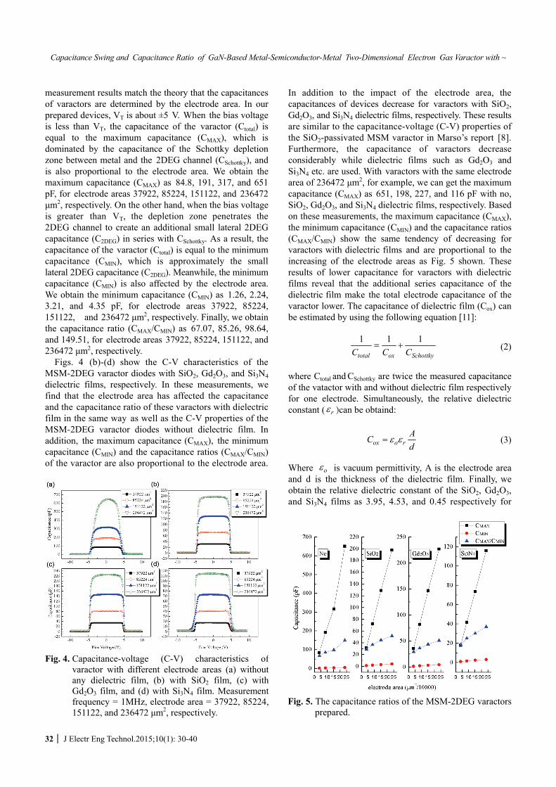
measurement results match the theory that the capacitances of varactors are determined by the electrode area. In our prepared devices, VT is about ±5 V. When the bias voltage is less than VT, the capacitance of the varactor (Ctotal) is equal to the maximum capacitance (CMAX), which is dominated by the capacitance of the Schottky depletion zone between metal and the 2DEG channel (CSchottky), and is also proportional to the electrode area. We obtain the maximum capacitance (CMAX) as 84.8, 191, 317, and 651 pF, for electrode areas 37922, 85224, 151122, and 236472 μm2, respectively. On the other hand, when the bias voltage is greater than VT, the depletion zone penetrates the 2DEG channel to create an additional small lateral 2DEG capacitance (C2DEG) in series with CSchottky. As a result, the capacitance of the varactor (Ctotal) is equal to the minimum capacitance (CMIN), which is approximately the small lateral 2DEG capacitance (C2DEG). Meanwhile, the minimum capacitance (CMIN) is also affected by the electrode area. We obtain the minimum capacitance (CMIN) as 1.26, 2.24, 3.21, and 4.35 pF, for electrode areas 37922, 85224, 151122, and 236472 μm2, respectively. Finally, we obtain the capacitance ratio (CMAX/CMIN) as 67.07, 85.26, 98.64, and 149.51, for electrode areas 37922, 85224, 151122, and 236472 μm2, respectively.
Figs. 4 (b)-(d) show the C-V characteristics of the MSM-2DEG varactor diodes with SiO2, Gd2O3, and Si3N4 dielectric films, respectively. In these measurements, we find that the electrode area has affected the capacitance and the capacitance ratio of these varactors with dielectric film in the same way as well as the C-V properties of the MSM-2DEG varactor diodes without dielectric film. In addition, the maximum capacitance (CMAX), the minimum capacitance (CMIN) and the capacitance ratios (CMAX/CMIN) of the varactor are also proportional to the electrode area.
In addition to the impact of the electrode area, the capacitances of devices decrease for varactors with SiO2, Gd2O3, and Si3N4 dielectric films, respectively. These results are similar to the capacitance-voltage (C-V) properties of the SiO2-passivated MSM varactor in Marso’s report [8]. Furthermore, the capacitance of varactors decrease considerably while dielectric films such as Gd2O3 and Si3N4 etc. are used. With varactors with the same electrode area of 236472 μm2, for example, we can get the maximum capacitance (CMAX) as 651, 198, 227, and 116 pF with no, SiO2, Gd2O3, and Si3N4 dielectric films, respectively. Based on these measurements, the maximum capacitance (CMAX), the minimum capacitance (CMIN) and the capacitance ratios (CMAX/CMIN) show the same tendency of decreasing for varactors with dielectric films and are proportional to the increasing of the electrode areas as Fig. 5 shown. These results of lower capacitance for varactors with dielectric films reveal that the additional series capacitance of the dielectric film make the total electrode capacitance of the varactor lower. The capacitance of dielectric film (Cox) can be estimated by using the following equation [11]:
1 1 1
total ox SchottkyC C C= + (2)
where Ctotal and CSchottky are twice the measured capacitance of the vatactor with and without dielectric film respectively for one electrode. Simultaneously, the relative dielectric constant ( rε )can be obtaind:
ox o rACd
ε ε= (3)
Where oε is vacuum permittivity, A is the electrode area and d is the thickness of the dielectric film. Finally, we obtain the relative dielectric constant of the SiO2, Gd2O3, and Si3N4 films as 3.95, 4.53, and 0.45 respectively for
Fig. 4. Capacitance-voltage (C-V) characteristics of varactor with different electrode areas (a) without any dielectric film, (b) with SiO2 film, (c) with Gd2O3 film, and (d) with Si3N4 film. Measurement frequency = 1MHz, electrode area = 37922, 85224, 151122, and 236472 μm2, respectively.
Fig. 5. The capacitance ratios of the MSM-2DEG varactors prepared.

Chu-Yeh Tien, Ping-Yu Kuei, Liann-Be Chang and Chien-Pin Hsu
http://www.jeet.or.kr │ 33
the electrode area is 236472 μm2. The results reveal that the quality of dielectric films processed by electron beam deposition is not as good as the samples processed by PECVD [8, 12-14].
In C-V measurement, it also shows that the transition voltages of the varactors with dielectric films prepared are approximately ±5 V the same in each case, differing from a previous report in which the transition voltage increases twice for the SiO2-passivated MSM varactor to unpassivated device [7-8]. Because the transition voltage depends on the 2DEG channel depleted completely, it also relate to the 2DEG carrier density [8]. As Fig. 1 (b) the samples prepared shown, the thinner of AlGaN layer and the lower mole fractions of Al are, the lower 2DEG carrier density results in lower transition voltage[15] than Marso’s device as Fig. 1 (a). Furthermore, the quality of the dielectric film processed by e-beam deposition is not as good as the samples processed by PECVD, the dielectric film/GaN interface state density is too high to increase the sheet carrier density of the 2DEG channel, so that the 2DEG channel is easily depleted with the same transition voltage of the unpassivated varactors [7-8].
Fig. 6 (a) shows the I-V characteristics of the MSM-2DEG varactors without dielectric films. The leakage current increases with the increasing of the electrode area. Because the MSM-2DEG varactor consists of two Schottky diodes connected back to back above the 2DEG channel, both the forward and reverse current are identical and symmetrical, and the reverse current is dominated by the Schottky diode under reverse bias [6]. The leakage current of these MSM-2DEG varactors are 10-8 A approximately. When the applied voltage higher than the transition voltage (±5 V in this study), the reverse-bias depletion zone penetrates the 2DEG channel and form a leakage current
path to the forward-bias depletion zone. The leakage current increases until saturation about 10-5 A.
Because a serious problem of AlGaN/GaN HEMT structure is the high gate leakage current, it can be partially suppressed by using the dielectric film deposition. Fig. 6 (b)-(d) show the I-V characteristics of the MSM-2DEG varactor diodes with SiO2, Gd2O3, and Si3N4 dielectric films, respectively. Although the leakage current increases with the increasing of the electrode area, for each dielectric film used, it reduces the leakage currents by three orders of magnitude from 10-5 A to 10-8 A (even more lower) even the input bias voltage higher than ±5 V. For the varactors with Si3N4 dielectric film as shown in Fig. 6 (d), the leakage current increases rapidly as the input bias voltage higher than ±7 V. That is because the lower energy gap (Eg) of Si3N4 [16], the capability of the leakage-current suppression of Si3N4 dielectric film is lower than the other two dielectric films as Fig. 6 (b)-(c) shown.
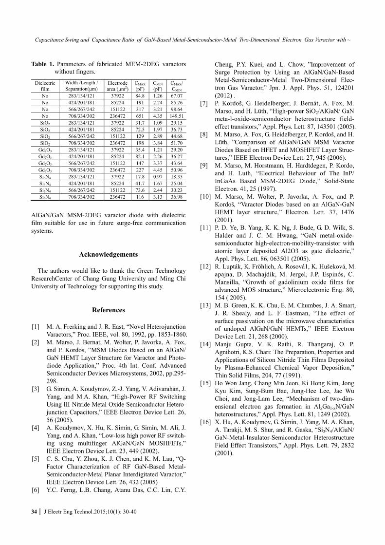
Base on the C-V and I-V measurements, the capacitance ratio is lowered to 18.35 and up to 149.51 while the varactors are with the Si3N4 film or without dielectric film, respectively. The varactor without any dielectric film has the highest capacitance ratio here, but the capacitance ratios of the varactors with SiO2 and Gd2O3 dielectric films are up more than 50 while the electrode area are 236472 μm2. Compared with previous reports [7-8], the varactors with the SiO2 and Gd2O3 dielectric films deposited by the E-beam deposition have the potential to offer the benefits of both high capacitance ratios and high capability of the leakage-current suppression. The geometry and capacitance parameters of the AlGaN/GaN MSM-2DEG varactor diodes are summarized in Table 1. The capacitance and capacitance ratios of devices depend on the varactors with different electrode areas as well as dielectric films.
5. Summary and Conclusions We have fabricated and studied AlGaN/GaN MSM-
2DEG varactor diodes by comparing the capacitance, capacitance ratio, transition voltage, and leakage current of these varactors with various electrode areas as well dielectric films (SiO2, Gd2O3, and Si3N4), respectively. The capacitances of the varactors vary with the electrode area and with different dielectric materials. The capacitance ratio is tunable from 18.35 to 149.51 for the varactors with the SiO2 film or without dielectric film, respectively. Compared with our previous study, a key finding in this study is that the transition voltage of each of the fabricated samples is about ±5 V. It is observed that the MSM-2DEG varactor without dielectric film is stable and suitable for devices requiring a high capacitance ratio. The varactors with the SiO2 and Gd2O3 dielectric films deposited by the E-beam deposition are up more than 50 and also offer the benefit of lower the leakage current. These properties of varactors with tunable capacitance ratios make the
Fig. 6. Current-voltage (I-V) characteristics of varactor withdifferent electrode areas (a) without any dielectric film, (b) with SiO2 film, (c) with Gd2O3 film, and (d) with Si3N4 film. Measurement frequency = 1MHz, electrode area = 37922, 85224, 151122, and 236472 μm2, respectively.
Capacitance Swing and Capacitance Ratio of GaN-Based Metal-Semiconductor-Metal Two-Dimensional Electron Gas Varactor with ~
34 │ J Electr Eng Technol.2015;10(1): 30-40
AlGaN/GaN MSM-2DEG varactor diode with dielectric film suitable for use in future surge-free communication systems.
Acknowledgements The authors would like to thank the Green Technology
ResearchCenter of Chang Gung University and Ming Chi University of Technology for supporting this study.
References
[1] M. A. Frerking and J. R. East, “Novel Heterojunction Varactors,” Proc. IEEE, vol. 80, 1992, pp. 1853-1860.
[2] M. Marso, J. Bernat, M. Wolter, P. Javorka, A. Fox, and P. Kordos, “MSM Diodes Based on an AlGaN/ GaN HEMT Laycr Structure for Varactor and Photo-diode Application,” Proc. 4th Int. Conf. Advanced Semiconductor Devices Microsystems, 2002, pp.295-298.
[3] G. Simin, A. Koudymov, Z.-J. Yang, V. Adivarahan, J. Yang, and M.A. Khan, “High-Power RF Switching Using III-Nitride Metal-Oxide-Semiconductor Hetero-junction Capacitors,” IEEE Electron Device Lett. 26, 56 (2005).
[4] A. Koudymov, X. Hu, K. Simin, G. Simin, M. Ali, J. Yang, and A. Khan, “Low-loss high power RF switch-ing using multifinger AlGaN/GaN MOSHFETs,” IEEE Electron Device Lett. 23, 449 (2002).
[5] C. S. Chu, Y. Zhou, K. J. Chen, and K. M. Lau, “Q-Factor Characterization of RF GaN-Based Metal-Semiconductor-Metal Planar Interdigitated Varactor,” IEEE Electron Device Lett. 26, 432 (2005)
[6] Y.C. Ferng, L.B. Chang, Atanu Das, C.C. Lin, C.Y.
Cheng, P.Y. Kuei, and L. Chow, ”Improvement of Surge Protection by Using an AlGaN/GaN-Based Metal-Semiconductor-Metal Two-Dimensional Elec-tron Gas Varactor,” Jpn. J. Appl. Phys. 51, 124201 (2012) .
[7] P. Kordoš, G. Heidelberger, J. Bernát, A. Fox, M. Marso, and H. Lüth, “High-power SiO2/AlGaN/ GaN meta-l-oxide-semiconductor heterostructure field-effect transistors,” Appl. Phys. Lett. 87, 143501 (2005).
[8] M. Marso, A. Fox, G. Heidelberger, P. Kordoš, and H. Lüth, ”Comparison of AlGaN/GaN MSM Varactor Diodes Based on HFET and MOSHFET Layer Struc-tures,” IEEE Electron Device Lett. 27, 945 (2006).
[9] M. Marso, M. Horstmann, H. Hardtdegen, P. Kordo, and H. Luth, “Electrical Behaviour of The InP/ InGaAs Based MSM-2DEG Diode,” Solid-State Electron. 41, 25 (1997).
[10] M. Marso, M. Wolter, P. Javorka, A. Fox, and P. Kordoš, “Varactor Diodes based on an AlGaN-GaN HEMT layer structure,” Electron. Lett. 37, 1476 (2001).
[11] P. D. Ye, B. Yang, K. K. Ng, J. Bude, G. D. Wilk, S. Halder and J. C. M. Hwang, “GaN metal-oxide-semiconductor high-electron-mobility-transistor with atomic layer deposited Al2O3 as gate dielectric,” Appl. Phys. Lett. 86, 063501 (2005).
[12] R. Lupták, K. Fröhlich, A. Rosová1, K. Hušeková, M. apajna, D. Machajdík, M. Jergel, J.P. Espinós, C. Mansilla, “Growth of gadolinium oxide films for advanced MOS structure,” Microelectronic Eng. 80, 154 ( 2005).
[13] M. B. Green, K. K. Chu, E. M. Chumbes, J. A. Smart, J. R. Shealy, and L. F. Eastman, “The effect of surface passivation on the microwave characteristics of undoped AlGaN/GaN HEMTs,” IEEE Electron Device Lett. 21, 268 (2000).
[14] Manju Gupta, V. K. Rathi, R. Thangaraj, O. P. Agnihotri, K.S. Chari: The Preparation, Properties and Applications of Silicon Nitride Thin Films Deposited by Plasma-Eehanced Chemical Vapor Deposition,” Thin Solid Films, 204, 77 (1991).
[15] Ho Won Jang, Chang Min Jeon, Ki Hong Kim, Jong Kyu Kim, Sung-Bum Bae, Jung-Hee Lee, Jae Wu Choi, and Jong-Lam Lee, “Mechanism of two-dim-ensional electron gas formation in AlxGa1-xN/GaN heterostructures,” Appl. Phys. Lett. 81, 1249 (2002).
[16] X. Hu, A. Koudymov, G. Simin, J. Yang, M. A. Khan, A. Tarakji, M. S. Shur, and R. Gaska, “Si3N4/AlGaN/ GaN-Metal-Insulator-Semiconductor Heterostructure Field Effect Transistors,” Appl. Phys. Lett. 79, 2832 (2001).
Table 1. Parameters of fabricated MEM-2DEG varactors without fingers.
Dielectric film
Width /Length / Separation(μm)
Electrode area (μm2)
CMAX (pF)
CMIN(pF)
CMAX/CMIN
No 283/134/121 37922 84.8 1.26 67.07No 424/201/181 85224 191 2.24 85.26No 566/267/242 151122 317 3.21 98.64No 708/334/302 236472 651 4.35 149.51
SiO2 283/134/121 37922 31.7 1.09 29.15SiO2 424/201/181 85224 72.5 1.97 36.73SiO2 566/267/242 151122 129 2.89 44.68SiO2 708/334/302 236472 198 3.84 51.70
Gd2O3 283/134/121 37922 35.4 1.21 29.20Gd2O3 424/201/181 85224 82.1 2.26 36.27Gd2O3 566/267/242 151122 147 3.37 43.64Gd2O3 708/334/302 236472 227 4.45 50.96Si3N4 283/134/121 37922 17.8 0.97 18.35Si3N4 424/201/181 85224 41.7 1.67 25.04Si3N4 566/267/242 151122 73.6 2.44 30.23Si3N4 708/334/302 236472 116 3.13 36.98
Chu-Yeh Tien, Ping-Yu Kuei, Liann-Be Chang and Chien-Pin Hsu
http://www.jeet.or.kr │ 35
Chu-Yeh Tien He received the M.E. degree from CCIT, NDU, Taiwan in 2000. He is currently working toward a Ph.D. degree. His current research areas include flip-chip IC configuration and ESD protection circuit design of HEMT devices.
Ping-Yu Kuei He received the M.E. andPh.D. degree in 1997 and 2003. He is currently an Associate Professor. His research interest is focused on the design and fabrication of optoelec-tronic and microwave devices such as HEMT, and solar cells.
Liann-Be Chang (M’95) received the B.S. and Ph.D. degree in 1980 and 1987. He is currently a Professor. His research interest is focused on the design and fabrication of optoelectronic and microwave devices such as LED, HEMT, and solar cells.
Chien-Pin Hsu He received the M.E. degree from CCIT, NDU, Taiwan in 2013. He is currently a developed engineer. His research interest interest is focused on the design and fabri-cation of the surge protection circuit design of HEMT devices.