Canada’s National Design Network – from nano to …asdn.net/ngc2009/presentations/presentations...
22
NGC / CSTC 2009 – McMaster University 1 Ian McWalter Canada’s National Design Network – from nano to macro
Transcript of Canada’s National Design Network – from nano to …asdn.net/ngc2009/presentations/presentations...
NGC / CSTC 2009 –
McMaster University 1
Ian McWalter
Canada’s National Design Network – from nano to macro
2
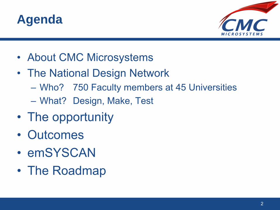
Agenda
•
About CMC Microsystems•
The National Design Network–
Who?
750 Faculty members at 45 Universities
–
What?
Design, Make, Test
•
The opportunity•
Outcomes
•
emSYSCAN•
The Roadmap

3
CMC Microsystems
•
An organization with a 25-year history of stimulating R&D–
Discovery (leading to publications) and –
Innovation (leading to products);–
Involving micro- and nano-scaletechnologies;
–
Through delivery of research infrastructure (tools) and
–
A path to commercialization.
•
A not-for-profit organization:–
Industry, university and other members.–
Headquarters in Kingston (Innovation Park at Queen’s University)
–
National test lab operation (U Toronto, McGill U, U Manitoba, Queen’s U)
–
Photonic project R&D office at the Canadian Photonics Fabrication Centre (NRC, Ottawa)
CMC enables and supports the creation and application of micro-
and nano-system knowledge by providing a national infrastructure for excellence in research and a path to commercialization of related devices, components and systems.
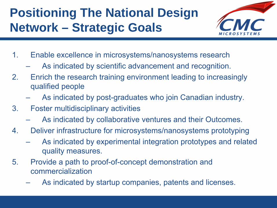
Positioning The National Design Network – Strategic Goals
1.
Enable excellence in microsystems/nanosystems research–
As indicated by scientific advancement and recognition.2.
Enrich the research training environment leading to increasingly
qualified people–
As indicated by post-graduates who join Canadian industry.3.
Foster multidisciplinary activities–
As indicated by collaborative ventures and their Outcomes.4.
Deliver infrastructure for microsystems/nanosystems prototyping–
As indicated by experimental integration prototypes and related quality measures.
5.
Provide a path to proof-of-concept demonstration and commercialization
–
As indicated by startup companies, patents and licenses.

ECE/EE 67%
Mechanical Eng. 9%
Computer Science 10%
Other Engineering 3%
Eng. Physics 2%
Physic 5%Chemistry 3%
Other 1%
Faculty Members by Discipline/Department, 2007
Registered University Users
~750 Registered Faculty Members 2008
More than 60 holders of Canada Research Chairs
5

Trend: The Changing Preferences of NDN Researchers in Areas of Application
Examples of Other include:
Natural Resources (Energy), Environment, Agriculture
Examples of Other include:Natural Resources (Energy), Environment, Agriculture
Registered faculty members whose interests were known -
1999: 163, 2003: 292, 2006: 504, 2007: 639, 2008: 753
Presenter
Presentation Notes
NSERC Proposal, Section 1.2, page 14, Figure 1.9

7
The Supply Chain: Some of the CMC Suppliers
MOSIS

8
Prototyping Technologies Used for about 400 NDN Projects Annually
•
Advanced and mature CMOS prototype manufacturing services from national and international manufacturers:–
65nm - 90-nm - 0.13 micron
–
0.18 micron - 0.35 micron - 0.8 micron–
Starting to use of 45 nm CMOS
–
2.5 GHz bipolar linear array (single layer metalization)•
MEMS prototyping :Surface/SOI; CMOS
•
Microfluidics prototyping: Dual plane in-channel electrode metallization technology; Closed microchannels glass networks
•
Photonics/Optoelectronics prototyping (silicon or III/V)
Technologies sourced from: CPFC/NRC, DALSA, Sound Technologies sourced from: CPFC/NRC, DALSA, Sound Design Technologies, Micralyne, IBM, MEMSCAP, Design Technologies, Micralyne, IBM, MEMSCAP, STMicroelectronics, TSMC, CMP, MOSIS, IMECSTMicroelectronics, TSMC, CMP, MOSIS, IMEC

9
Operating 4 Test Laboratories
Mixed Signal (McGill )PI: Gord RobertsTeradyne FLEX Tester96 CH digital @ 200 MHz24 bit analog I/O16 bit high speed analogRF to 6 GHz High power pulse
Digital (Toronto) PI: Glenn GulakVerigy 93000 Tester500 channels @ 600-1250 MHz256 channels @ 500 MHz3 channels RF @ 6 GHz (modulated)Digital virtual test via emulation20 GS/s digital storage scope
Photonics (Queen’s)PI: John Cartledge40 GB/s and 10 GB/s BERTsDevice testing for E/O, O/O and O/ESignal characterization
(electrical and optical)System characterization 10-160 Gb/s Multi-channel, multi-span transmission
RF(mm-wave) (Manitoba)PI: Greg Bridges40 MHz to 110 GHz RF test capabilitySemi-automatic wafer proberSignal characterization to 110 GHzSignal generation to 110 GHzNoise figure analysisPower measurement

10
Photonics Products and Services Overview
•
CAD tools for–
Mode solving–
BPM simulation–
Design optimization–
Physical layout and verification of optical components, customized for CMC’s prototype fabrication services
•
Prototyping–
III-V and silicon-based prototyping services provided in partnership with the Canadian Photonics Fabrication Center (CPFC)
–
New: SOI passive waveguide photonics through IMEC (Belgium)
•
Extensive test resources, including–
Laser/waveguide test station–
Vertical fibre coupling–
Advanced Photonic Systems Lab
•
Training–
Silicon Nanophotonics Fabrication Graduate Course (in partnership with UBC)

11
Microfluidics
Microelectronics
MEMSPhotonics
Embedded Software
Opportunity…Microsystems Influence All Sectors: Jobs, Growth, R&D
Health Care
Environment Transportation
Aerospace
Security Agriculture
Energy
BiotechnologyCommunication
s
Presenter
Presentation Notes
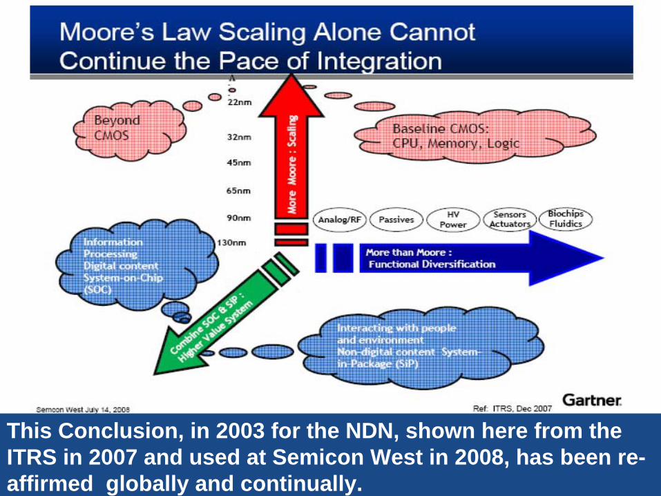
This Conclusion, in 2003 for the NDN, shown here from the ITRS in 2007 and used at Semicon West in 2008, has been re- affirmed globally and continually.

13 <Project Name> DP1
Design Hardware Infrastructure and IP 70% increase in FPGA-based platforms; 20X- 60X increase in CAD tool disk capacity • FPGA-based System-level Prototyping Systems (700)
o Xilinx Virtex-II Pro FPGA (310 systems) • ARM Rapid Prototyping Platforms with Mentor RTOS (58) • Multi-Processor SOC Methodology Platforms (8)
o System-level simulation and FPGA implementation • MEMS-FPGA Platforms (8)
o Analog-interfacing, HV amplifier • Tensilica-configurable processor IP
o FPGA netlist generation • Supported Technology Configuration (STC) Disks (36):
o 3TB (23)/2TB (4)/1TB (1) ; 50GB-219GB (8) • MIPS microprocessor (6) • Tensilica-configurable processor IP
o FPGA netlist generation
Design Tools 2.5X increase in capability from 2004 Microelectronics/microsystems • Cadence - 38 universities • Mentor HEP - 36 universities • Synopsys - 37 universities • Xilinx - 36 universities • Celoxica - 23 universities • Coware - 27 universities • Forte - 16 universities • Matlab - 34 universities MEMS/microfluidics • ANSYS - 16 universities • MEMSPro - 22 universities • COMSOL - 9 universities • Coventor - 9 universities Photonics • Design Workshop - 18 universities
• Optiwave - 7 universities •Rsoft - 9 universities
Training and Support2X training events with focus on MEMS and photonics CAD Training Courses
2004-2005: Matlab , Altera MIPS Microprocessor
• 2006-2007: ANSYS; Coventor ; MEMSPro; Tensilica Microprocessor
• 2007-2008: Design Workshop ; Tensilica; Xilinx
• 2008-2009: ANSYS; Comsol ; Coventor; MEMSPro
• Over 1000 support interactions annually
Methodology and KitsStrong emphasis on accelerating research results through development and dissemination of flows, user guides and Application Notes • Embedded Software,
Memory Integration and DFT Flows
• 52 Application Notes • 20 Tutorials • 40 Getting-Started/User
Guides • 10 Methodology Guides • 100 kits and kit upgrades
• 10 Reference Designs • Digital, Analog, RF and MEMS
Flows
Custom Integration Projects Support for 64 custom ntegration projects in areas such as:
Flip chipping Surface functionalization Ceramic carriers Photonic packaging Folded PCBs Selective encapsulation Implantable electrodes Vacuum packaging
NATIONAL DESIGN NETWORK 2008 Impact
Over 750 academic faculty and 2000 PhD and MSc students at 45 universities benefitted from NDN services in areas related to microsystems
research. More than 450 CAD tool licenses were distributed,
370 chip designs fabricated, some 200 test transactions conducted and 35 custom
integration projects completed.
Microsystems FabricationOver 1800 designs fabricated for 160 researchers in 27 universities Microelectronics • CMOS (nm): 65 , 90 • CMOS (micron): 0.13; 0.18;
0.35; 0.5 ; 0.8 • 2.5 GHz Linear Array Photonics • InP; GaAs ; SOI MEMS • PolyMUMPs ; SOI ;
MetalMUMPS Microfluidics • Glass-based, single channel Integrated electronics • MEMS post-processing
on 0.8-micron CMOS • Microfluidics with
embedded electrodes MNT Lab Access • MNT Facilities Catalog • MNT Travel & Fabrication
Awards
Test and MeasurementNational Microelectronics and Photonics Testing Collaboratory implemented and MEMS/microfluidics testing solutions delivered. • Microfluidics System
Prototyping Carrier Platform • 140-pieces leading-edge
photonic test equipment including 10 GB/s and 40GB/s BERTs, DQPSK
• Industry-standard ATE o Verigy 93000 Digital /RF
SOC Tester o Teradyne FLEX mixed –signal
tester • RF Test capability spanning
40MHz to 110 GHz • MEMS/microfluidics parametric
testing, high-speed actuation analysis
Denotes products/ services introduced to the NDN during the 2004-2009 period

14 14
Designs• Microelectronics• Microsystems
Fabricated Designs• Microelectronics• Microsystems
Tested Prototypes• Microelectronics• Microsystems··
• An Increasingly Competitive Microsystems Industry(both Nationally and Internationally) with SignificantEconomic and Social Benefits for Canada
• More Highly Skilled Microsystems Professionals Enabled
Deliver Products and Services
Ulti
mat
eO
utco
mes
(5+
year
s)
Inte
rmed
iate
Out
com
es(2
-4 y
ears
)
Imm
edia
teO
utco
mes
(<1
year
)
Out
puts
Act
iviti
es FabricationServices
Design Tools andMethodologies
Testing Productand Services
Deliver Trainingand Support
Promoting, Liaising,Networking with Clients, Industry,
and Other Stakeholders
LegendUG: undergraduatePG: postgraduateCRC: Canada Research Chairs
Performance Management MODEL –
Outcomes 2008
Updated: 31 March 2009
285 University collaborations with Canadian industry for $14.9M Support; 22 Licenses; 72 Patents; 6
Startups; 75 University collaborations with foreign industry for $2.7M
Support
753 Faculty (including 68 CRCs, 7 NSERC Chairs, 3 both)
339 PG Courses 362 UG Courses
1997
PG Students
268 Faculty• Tutorials• Workshops• Forums• User Groups
• Meetings/Symposia• Promotional Material• Success Stories• Newsletters• Collaboratory• Discussion Groups
• Cost-effective Research Excellence Enabled• Students More Capable of Using Industry Standard Tools• Students More Skilled in Microelectronic/Microsystems
Design, Build and Test
• Increased Awareness of CMC’s Role• More Timely, Informed, and Consistent Messaging
Among Partners and Stakeholders• Better Alignment of CMC and Client Expectations
• Increased Commercialization of MicrosystemsResearch Including Spinoffs
• A Larger Pool of Highly Skilled Microsystems Professionals
• More Integrated, Multi-sectorial Teams of Innovators• Increased Opportunities and Resources for
Collaborative Research in Microsystems
503
PG students move to Canadian Industry180 Awards 2275 Publications

15
NDN Researchers’ Preferred Areas of Technology Application, 2008 and Projected to 2014
2008: Actual for 753 Researchers 2014: Projected for 1185 Researchers
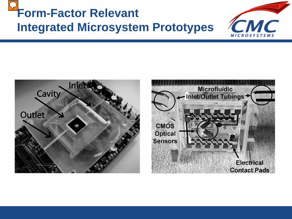
Form-Factor Relevant Integrated Microsystem Prototypes
Presenter
Presentation Notes
Figure 1.2
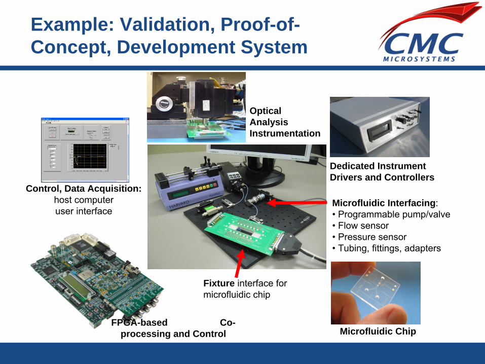
Example: Validation, Proof-of- Concept, Development System
Optical Analysis Instrumentation
Microfluidic Interfacing:• Programmable pump/valve• Flow sensor• Pressure sensor• Tubing, fittings, adapters
Fixture interface formicrofluidic chip
FPGA-based Co- processing and Control Microfluidic Chip
Control, Data Acquisition:host computeruser interface
Dedicated Instrument Drivers and Controllers

Example: Proof-of-Concept Development
reverse side viewchip antenna EMR shield layer
Sensor head
3-axisaccelerometer
Master processor and radio
Data acquisition
IDC20
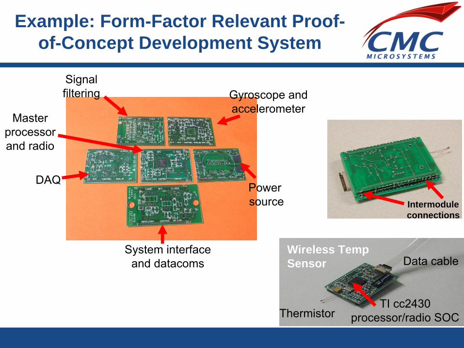
Example: Form-Factor Relevant Proof- of-Concept Development System
Intermoduleconnections
DAQ
Masterprocessorand radio
Gyroscope andaccelerometer
Power source
System interfaceand datacoms
Signalfiltering
Thermistor
Data cable
TI cc2430processor/radio SOC
Wireless TempSensor
20
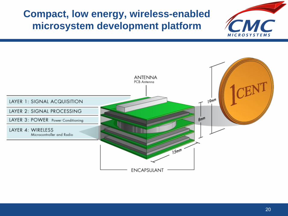
Compact, low energy, wireless-enabled microsystem development platform
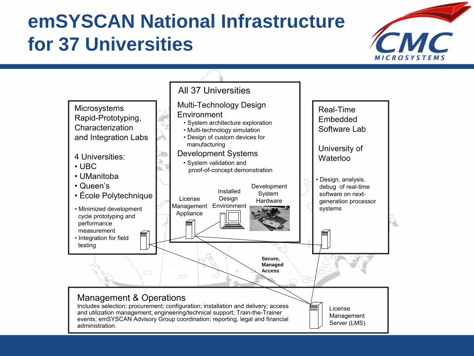
emSYSCAN National Infrastructure for 37 Universities
MicrosystemsRapid-Prototyping,Characterizationand Integration Labs
4 Universities:• UBC• UManitoba• Queen’s• École Polytechnique
Management & OperationsIncludes selection; procurement; configuration; installation and delivery; access and utilization management; engineering/technical support; Train-the-Trainer events; emSYSCAN Advisory Group coordination; reporting, legal and financial administration.
License ManagementServer (LMS)
All 37 Universities
Secure,Managed Access
Real-Time Embedded Software Lab
University of Waterloo
Multi-Technology Design Environment
Development Systems• System validation and
proof-of-concept demonstration
• System architecture exploration • Multi-technology simulation• Design of custom devices for
manufacturing
DevelopmentSystem
HardwareLicenseManagement
Appliance• Minimized development
cycle prototyping and performance measurement
• Integration for field testing
• Design, analysis, debug of real-time software on next-generation processor systems
InstalledDesign
Environment

The Resulting Infrastructure Technology Roadmap
2009 20112010 20132012 2014Roadmap Period of Interest: April 2009 to March 2015
Technology for Devices, Structures and Transducers (sensors and actuators)
Integrated Microsystem Architecture Attributes
Design Methodology
Test Methodology
Legend: Arrows indicate continuing enhancement or new options.
Kit: digital
Kit: RFKit: analog
Footprint: 10 cm3 (includes folded PCB)Stack: 5 layers, boardsPower: mWRF centre: 430MHz, 870MHz, 2.5GHz
Footprint: 1 cm3
Stack: TSV devicesPower: nW
Design-for-assembly (flow)
Interposer: embedded passives
Fixturing: microfluidics
GaN:
0.8µm Ft~ 20GHz CMOS: 800nm to 45nm
GaN:
0.4µm Ft~ 60GHz GaN:
Ft~ 125GHzCMOS: 32nm
Substrate: LTCC
Power: battery Power: scavenging Power: scavenging/implantable
Coatings: bio-compatibleCoatings: organic
Fixturing: 600MHz digital
Interposer: embedded activeCoatings: inorganic
Power: PV/solar
Photonic crystals/SOI III-V Qdot lasers III-V Qwell intermixing Photonics/GaN III-V Qcascade structures
Si-photonics Si-fluidicsMicrofluidicsMEMS
Standard, scalable system driver and test interface
High-speed clock and data recovery modules
Interfaces optimised for bench-top multi-sensor system prototyping
Substrate: RF signal optimised
Substrate: RF+ microfluidic optimised
Substrate: photonic+ microfluidic optimised
Si-other enhancements
Kit: MEMSKit: microfluidics
Kit: Multi-tech prototyping flow
New baseline instrumentation cage and racked instruments
Extend rack options for select technologies (photonics/microfluidics)
Instrument signal sensitivity on femto-scale
100 GHz BERTPortable environmental test chambers
Fixturing: multi-technologyFixturing: photonics
Fixturing/assembly: small footprint optics
SiC substrate technologies
passive, COTS, chip-scale … Antenna …active, tunable, monolithically integrated
Hours/days .. Operating time … Years/indefinite2 (accelerometer, temp) .. Add-in sensor options … 8
Programmability: small footprint flash, register setup
Programmability: SDR, reconfigurable hardware
SIP test interface
MEMS test module (optical, 20 KHz)
MEMS resonator
Visible λ
test 100 Ghz Telecom test THz component test
Simulation: co-simulation methods and portfolio of point simulators on-demand
Embedded software debug and on-line lab.
Condition telemetry (hardware, software)
Nanotechnology region epi lift-off
Nano-scale wire interconnect
Near IR λ
test
Multi-processor debug Code parallelization tools Kit: real-time operations Communications protocol stack tools
Mixed-signal FPGA
Presenter
Presentation Notes
NATIONAL DESIGN NETWORK Advantage is gained by NDN faculty members, post-graduate students, their direct collaborators and private-sector and public sponsors by conducting research using MNT platform technologies and research value-adding intellectual property that follow an integration roadmap: that expects investigation and use of microscale and nanoscale physical technologies (principally microelectronics), embedded software and novel materials; leads to heterogeneous 3D form-factor microsystems; and anticipates advances in the individual technologies, in the means of their integration and in reduction in some feature sizes by an order of magnitude to the 1 to 10 nm range. In terms often used, this is a NDN view of how to transition to a more “More than Moore” R&D environment.