CAN to Analog Converter SD0707 Shefali Dhaka Josh Schroeder Dan Williams.
56
CAN to Analog Converter SD0707 Shefali Dhaka Josh Schroeder Dan Williams
-
Upload
martin-neal -
Category
Documents
-
view
218 -
download
2
Transcript of CAN to Analog Converter SD0707 Shefali Dhaka Josh Schroeder Dan Williams.

CAN to Analog Converter
SD0707Shefali DhakaJosh SchroederDan Williams

Introduction
Client: Sauer-Danfoss Client Representative: Lincoln Davidson Faculty Advisor: Dr. Nelson

Introduction
Device reads CAN messages Uses the CAN data to generate an analog output The arbitration ID of the CAN component will
determine how the message is interpreted User configures
Output Range (between -5 and 5 volts) Data Type of message Bit Order (Intel, Motorola)

Digital Hardware Requirements
We are to use components that Sauer-Danfoss uses in their own designs whenever possible
A microcontroller will be used to accept and interpret CAN messages
The micro must be able to communicate over RS232 for debugging
The micro must have access to a large amount of memory
DAC must have 16 bits of resolution

Software Requirements
Labview will be used to create a configuration program capable of changing how the CAN message is to be interpreted.
The user should be able to save new configurations of how the message is interpreted
The software on the microcontroller will be programmed through CAN
New user configurations will be retained after a power cycle
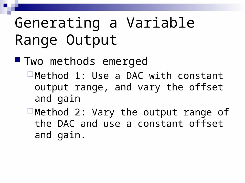
Generating a Variable Range Output Two methods emerged
Method 1: Use a DAC with constant output range, and vary the offset and gain
Method 2: Vary the output range of the DAC and use a constant offset and gain.

Generating a Variable Range Output Method 1
Two digital potentiometers could be used in a differential op-amp circuit
One to adjust the offsetThe other to adjust the gain
Method 2An extra 16 bit DAC could be used to adjust
VREFH & VREFL creating a variable output range

Generating a Variable Range Output Method 1: Advantages
Cost: Dual digital potentiometers prices range from about 1 to 5 dollars
Reduce the number of components Method 1: Disadvantages
Low number of distinct stages (usually 256)Not a component Sauer-Danfoss uses

Generating a Variable Range Output Method 2: Advantages
Has high resolution (16 bits)Can use parts Sauer-Danfoss typically usesReduces software complexity
Method 2: DisadvantagesCost: $12 per chip

Generating a Variable Range Output We chose Method 2
The higher resolution allows us to better match the users specifications
Reduces the complexity of the analog circuitryCan use Sauer-Danfoss partsWe were advised that digital potentiometers
can be unreliable

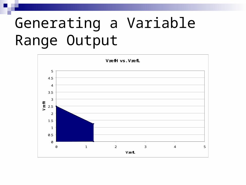
Generating a Variable Range Output Use the DAC8554 with SPI Output equation
VOUT = (Din/65535)*(VREFH - VREFL) + 2VREFL
The output range is anywhere between 0 and 2.5 volts
Minimum output is 2VREFL => Max VREFL = 1.25 V
Maximum output is VREFH + VREFL => Max VREFH = 2.5 V

Generating a Variable Range Output Design uses 5V and 0V as our VREFH & VREFL for
our first DAC Problem: only a small amount of the 1st DAC’s
resolution is used
DAC
VREFH
VREFL
VOUTA
VOUTB
DAC
VREFH
VREFL
VOUTA
5V(0…2.5V)(0…2.5V)
(0…1.25V)
VrefH vs. VrefL
0
0.5
1
1.5
2
2.5
3
3.5
4
4.5
5
0 1 2 3 4 5
VrefL
Vre
fH
Generating a Variable Range Output

Generating a Variable Range Output Solution: use voltage dividers to the reduce the
output voltage
DAC
VREFH
VREFL
VOUTA
VOUTBDAC
VREFH
VREFL
VOUTA
5V
(0…2.5V)(0…2.5V)
(0…1.25V)
R
R
R
3R
(0…5V)
(0…5V)

Digital Components
PIC24 was chosen as our microprocessor Bootloader and other code from Sauer-Danfoss can be
used EEPROM with I2C interface stores user
configuration data RS232 transceiver allows for debugging CAN transceiver
Programming PIC Receiving user configurations Receiving digital messages to convert to analog

Digital Components

Digital Components

Software

User Configuration Data File
Each CAN component must have a configuration file stored in the EEPROM
User Configuration Data File
Value # of bits
Component ID 29
Max Analog Out 16
Min Analog Out 16
Max Digital In 64
Min Digital In 64
Data Type (signed/unsigned int, float) 2
Message Bit Order 384
Total 575
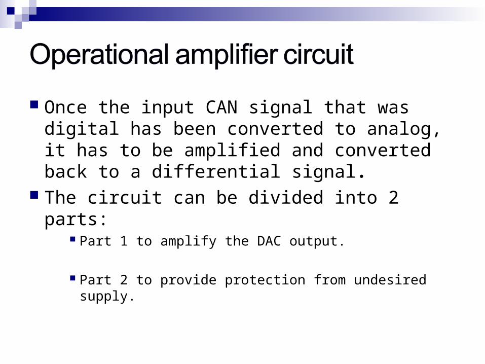
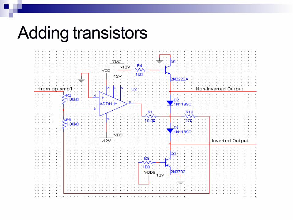
Once the input CAN signal that was digital has been converted to analog, it has to be amplified and converted back to a differential signal.
The circuit can be divided into 2 parts: Part 1 to amplify the DAC output.
Part 2 to provide protection from undesired supply.
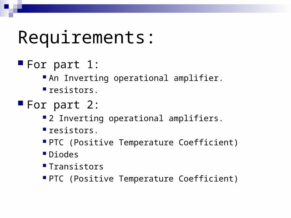
Requirements: For part 1:
An Inverting operational amplifier. resistors.
For part 2: 2 Inverting operational amplifiers. resistors. PTC (Positive Temperature Coefficient) Diodes Transistors PTC (Positive Temperature Coefficient)

Low noise op-amps were required for obvious reasons. Quad op-amps so there are easy and clean connections
on the PCB. High Gain bandwidth product. Low input offset voltage: It is a direct DC error. Low equivalent input noise voltage :
Noise = (input noise voltage)* (bandwidth)^1/2; So, it is very important to keep this low. Slew rate: to stabilize our output from the op-amp, a low
slew rate was desired(somewhere around a 50V/ms) Low offset voltage High temperature range: -40 to 85 degree Celsius for
use in any environment. High common mode rejection ratio: about 90-100 dB High open loop gain: It ensures higher DC accuracy.

Part 1: So this op amp will be used to amplify the
signal coming in from the D2A (VD2A) to a 5V as per the following equation:
Vout= 4 * (VD2A -1.25) This op amp1 is only used to generate the
desired output and supply it to the next two circuits that provide the protection (Part 2 ).

We decided on using an Inverting amplifier.Why? Because it has a negative feedback which is
good as positive feedback tends to increase oscillation effects.
Input the DAC output at the negative of the op amp to stabilize the inputs.
Resistor values R5 : R7 = 1 : 4
Thus, we get the negative output which is further fed into part 2.


Having some sort of safety provided between the op amp and the point where any voltage can be applied by the user is extremely important as then we have a secure device which is not prone to failures pertaining to accidental mistakes made by the user.

Put in a fuse:
Problem: Fuse would blow off and the user will have to take
the pain of changing the fuse.

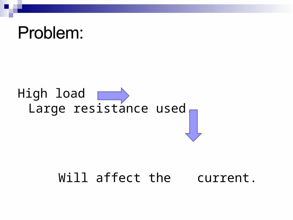
High load Large resistance used.
Will affect the current.
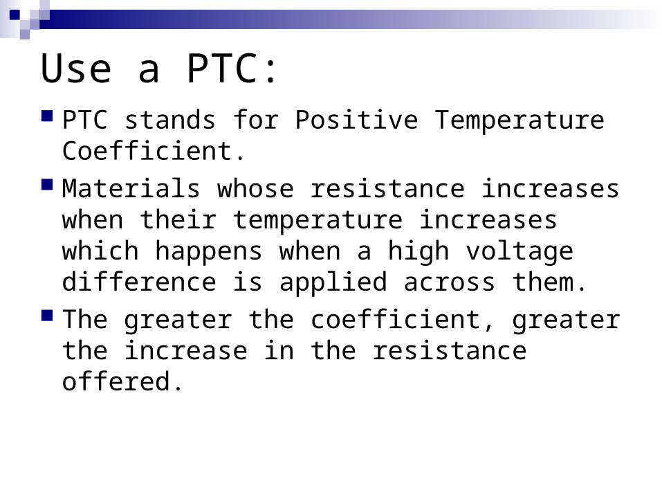
Use a PTC: PTC stands for Positive Temperature
Coefficient. Materials whose resistance increases
when their temperature increases which happens when a high voltage difference is applied across them.
The greater the coefficient, greater the increase in the resistance offered.

We use a 27 ohm PTC as that is what is used by Sauer Danfoss.
Problem: This is good and can be used but its increase in
resistance might not keep up if the applied voltage is extremely high.
So, we put a PTC instead of the normal resistance that was shown in the previous schematic, this reduces the current flowing through it to an extent and now we can have something else added so the remaining current is drained to someplace instead of going into the op amp.
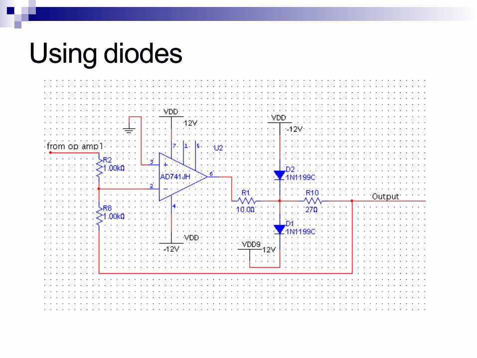

Diodes All the current into+/-12V
might not take such high current

Match not only the ratio of resistances at both the positive and the negative pins of the op-amp but try matching their values also; sometimes under high voltages this induces some oscillations in the output of the op-amp.
Equations used: Op-amp equation: Vout = Gain (Vd2a - Voffset) Voltage divider: Vout = (R1/R2)*gain


Power Distribution
Power Requirements Power Protection Switching Regulators Switching Inverters Voltage References

Power Requirements
9 to 40 Volt Input Protection against
Battery Reversal Protection from
Voltage Spikes
Voltages Needed1. 12 Volts
2. -12 Volts
3. 5 Volts
4. 5 Volt Reference with 0.1% Accuracy
5. 3.3 Volts

RBO40-40G
Protects against Voltage Spikes Prevents Damage from Battery Reversal Clamps off voltages over 40 Volts Small Size for what it does

RB040-40G
1 2 3
9 – 40 V
NC
1) Input2)NC
3)Output
GND
Vout
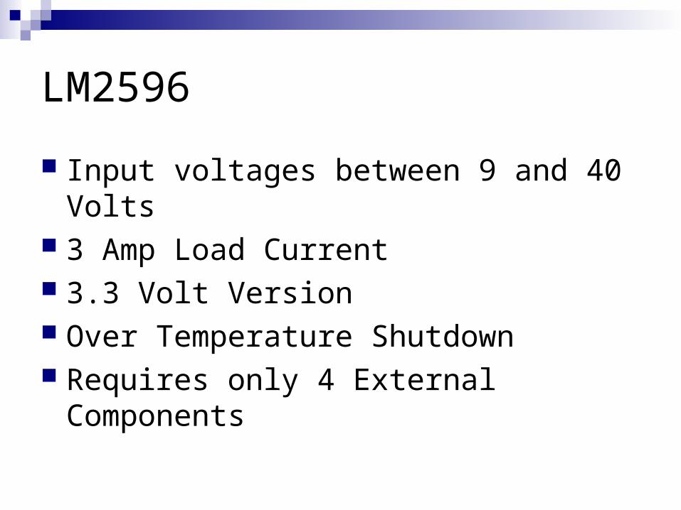
LM2596
Input voltages between 9 and 40 Volts 3 Amp Load Current 3.3 Volt Version Over Temperature Shutdown Requires only 4 External Components

RB040-40G
1 2 3
5 3
1
4
2
47K6.8uH
LM25963.3
33E-6HL
6 V
3.3 V
Cout
Cin
NC
L= 33uH L40Cin = 680uF 50V (Panisonic HFQ or
Nichicon PL)Cout= 330uF 6.3V (AVX TPS or
390uF 6.3V Sprague 595D series)
1) Vin2)Output3) GND
4) Feedback5) On/Off
1) Input2)NC
3)Output
GND

LM2731
Fully Adjustable Version Can Boast 3.3 Volts up to 20 Volts Uses small Capacitors and Inductors Small SOT-23 Package 8 External Components

V In
SHDN
SW
FB
LM2731 A = 5VB=3.3 V
6.8uH
40.5K
470pF
13.3K
2.2uF
47K
22uF
GND
1) SW2)GND3)FB
4)SHDN5) Vin
51K
R3
C1
R3
L
R1
R2
Cf
C2
D

Vin
SHDN
SW
FB
6.8uH
117K
270pF 10uF
13.3K
2.2uF
51K
A= 3.3VLM2731
12V
GND
C1
R3
L
D
R1
C2
Cf
R2
1) SW2)GND3)FB
4)SHDN5) Vin

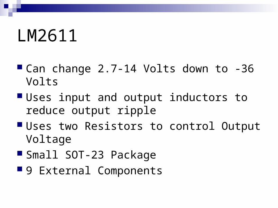
LM2611
Can change 2.7-14 Volts down to -36 Volts Uses input and output inductors to reduce
output ripple Uses two Resistors to control Output Voltage Small SOT-23 Package 9 External Components

LM26115
42
3
1
1) SW2)GND3) NFB4)SHDN
5) Vin
22uH 22uH1uF
1000pF
D22uF29.4K
3.3K
22uF
12V -12V
Cin
Cout
Cff
CcukL1 L2


LM4041
Can supply a Reference voltage up to 15V with better than 0.1% Accuracy
Small SOT-23 Package Uses only three external resistors

12V
1.4K
10K
3K
Lm4041 ADJ
1
2
3
1) FB2) +3) -
RS
R1
R2
5V REF

Future Tasks
Continue troubleshooting design Design and build PCB Write software
C code for PICLabview user configuration

Timeline
Task Desription Duration Start Date End Date
Functional Block Diagram 5 days 1/29/2007 2/2/2007
Gather Componants Lists (ALL) 18 days 2/3/2007 2/27/2007
Design Ideas (All) 44 days? 2/27/2007 4/26/2007
Rough Schematic (All) 20 days 4/1/2007 4/26/2007
Gather Components (All) 8 days 4/27/2007 5/8/2007
Test Components (Josh and Dan) 23 days 5/9/2007 6/8/2007
Break 77 days 5/14/2007 8/28/2007
Design and order Board (Josh and Shefali) 31 days 9/28/2007 11/9/2007
Test Prototype Board (Josh and Shefali) 18 days 9/17/2007 10/10/2007
Software for PIC (Dan and Shefali) 18 days 9/17/2007 10/10/2007
Begin Labview Configuration Program (Dan) 21 days 10/5/2007 11/2/2007
Test Software (Dan) 14 days 11/5/2007 11/22/2007
Test Hardware (Josh and Shefali) 14 days 11/23/2007 12/12/2007
Revisions/Modifications (ALL) 18 days 11/28/2007 12/21/2007
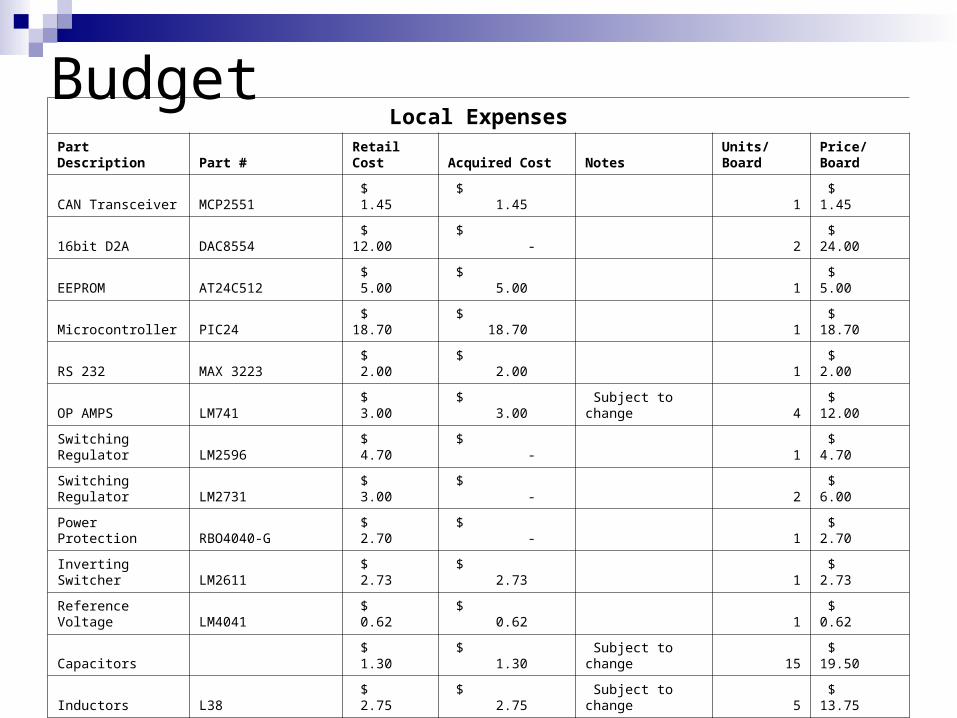
Local ExpensesPart Description Part # Retail Cost Acquired Cost Notes Units/Board Price/Board
CAN Transceiver MCP2551 $ 1.45 $ 1.45 1 $ 1.45
16bit D2A DAC8554 $ 12.00 $ - 2 $ 24.00
EEPROM AT24C512 $ 5.00 $ 5.00 1 $ 5.00
Microcontroller PIC24 $ 18.70 $ 18.70 1 $ 18.70
RS 232 MAX 3223 $ 2.00 $ 2.00 1 $ 2.00
OP AMPS LM741 $ 3.00 $ 3.00 Subject to change 4 $ 12.00
Switching Regulator LM2596 $ 4.70 $ - 1 $ 4.70
Switching Regulator LM2731 $ 3.00 $ - 2 $ 6.00
Power Protection RBO4040-G $ 2.70 $ - 1 $ 2.70
Inverting Switcher LM2611 $ 2.73 $ 2.73 1 $ 2.73
Reference Voltage LM4041 $ 0.62 $ 0.62 1 $ 0.62
Capacitors $ 1.30 $ 1.30 Subject to change 15 $ 19.50
Inductors L38 $ 2.75 $ 2.75 Subject to change 5 $ 13.75
Diodes MBR0520LT1GOSCT $ 0.25 $ 0.25 3 $ 0.75
Diodes 1N5825 $ 7.50 $ 7.50 Subject to change 3 $ 22.50
Resistors $ 0.25 $ 0.25 Subject to change 22 $ 5.50
CAN card $ 500.00 $ - Client Expense 1 $ 500.00
Enclosure $ 15.00 $ 15.00 1 $ 15.00
PCB Board $ 100 $ - Client Expense 1 $ 100.00
Total Price/Board: $ 141.90
# of Boards: 2
Total Price: $ 283.80
Budget

Budget
Total Budget Granted by NDSU $ 200.00
Money Spent Money Remaining
Component Total Total
Resistors $ 15.35 $ 184.65
Almost every component we have dealt with we have acquired as free samples
It is hard to project what we will get for free and what we will have to pay for

Summary
We are well on our way to completing the project by the end of next semester.
We have completed a schematic We have run simulations and tested
physical circuits We feel our design is complete and we are
ready to move onto implementation