C6000 Embedded Design Workshop - Squarespace · DSP Core C6000 Embedded Design Workshop - C6000...
164
C6000 Embedded Design Workshop - Cover 0 - 1 C6000 Embedded Design Workshop Student Guide C6000 Embedded Design Workshop Student Guide (includes slides & lab procedures), Rev 2.3 – Dec 2016 in association with
Transcript of C6000 Embedded Design Workshop - Squarespace · DSP Core C6000 Embedded Design Workshop - C6000...
C6000 Embedded Design Workshop - Cover 0 - 1
C6000 Embedded Design Workshop
Student Guide
C6000 Embedded Design Workshop
Student Guide (includes slides & lab procedures), Rev 2.3 – Dec 2016
in association with
Notice
0 - 2 C6000 Embedded Design Workshop - Cover
Notice
These materials, slides, labs, solutions are essentially creative commons license because they are stored on a public website. However, the most current author, Mindshare Advantage LLC, must be contacted before these materials are used in any other form for presentations, college course material or for any other purpose. These materials are being updated and kept current by Mindshare Advantage LLC but are used “in association with Texas Instruments” with their permission to update and maintain as current.
Mindshare Advantage reserves the right to update this Student (and Lab) Guide to reflect the most current product information for the spectrum of users. If there are any differences between this Guide and a technical reference manual, references should always be made to the most current reference manual and/or datasheet. Information contained in this publication is believed to be accurate and reliable. However, responsibility is assumed neither for its use nor any infringement of patents or rights of others that may result from its use. No license is granted by implication or otherwise under any patent or patent right of Texas Instruments or Mindshare Advantage.
If you have any questions pertaining to this material, please contact Mindshare Advantage at:
www.MindshareAdvantage.com
Revision History
2.00 March 2016 – entire workshop updated to the latest tools (slides, code, labs, etc.)
2.1 July 2016 – updated labs/solutions files, minor errata
2.3 Dec 2016 – updated labs/solutions files, minor errata
C6000 Embedded Design Workshop - C6000 Introduction 11 - 1
C6000 Introduction
Introduction
This is the first chapter that specifically addresses ONLY the C6000 architecture. All chapters from here on assume the student has already taken the 2-day TI-RTOS Kernel workshop.
During those past two days, some specific C6000 architecture items were skipped in favor of covering all TI EP processors with the same focus. Now, it is time to dive deeper into the C6000 specifics.
The first part of this chapter focuses on the C6000 family of devices. The 2nd part dives deeper into topics already discussed in the previous two days of the TI-RTOS Kernel workshop. In a way, this chapter is “catching up” all the C6000 users to understand this target environment specifically.
After this chapter, we plan to dive even deeper into specific parts of the architecture like optimizations, cache and EDMA.
Objectives
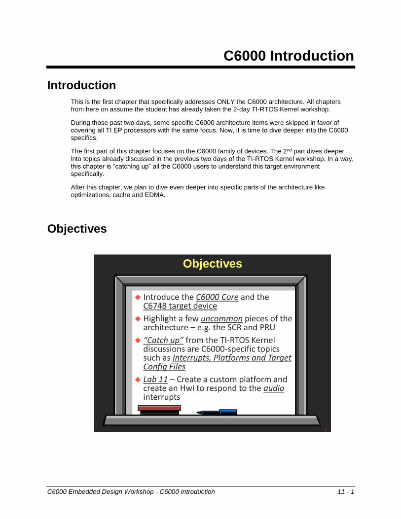
Objectives
Introduce the C6000 Core and the C6748 target device
Highlight a few uncommon pieces of the architecture – e.g. the SCR and PRU
“Catch up” from the TI-RTOS Kernel discussions are C6000-specific topics such as Interrupts, Platforms and Target Config Files
Lab 11 – Create a custom platform and create an Hwi to respond to the audiointerrupts
4
Module Topics
11 - 2 C6000 Embedded Design Workshop - C6000 Introduction
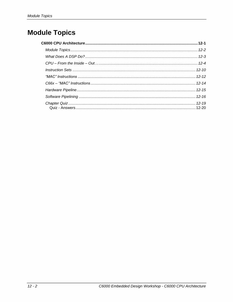
Module Topics
C6000 Introduction .................................................................................................................... 11-1
Module Topics ......................................................................................................................... 11-2
TI EP Product Portfolio............................................................................................................ 11-3
DSP Core ................................................................................................................................ 11-4
Devices & Documentation ....................................................................................................... 11-6
Peripherals .............................................................................................................................. 11-7 PRU ..................................................................................................................................... 11-8 SCR / EDMA3 .................................................................................................................... 11-9 Pin Muxing......................................................................................................................... 11-10
Example Device: C6748 DSP ............................................................................................... 11-11
Choosing a Device ................................................................................................................ 11-12
C6000 Arch “Catchup” .......................................................................................................... 11-13 C64x+ Interrupts ................................................................................................................ 11-13 Event Combiner ................................................................................................................ 11-14 Target Config Files ............................................................................................................ 11-15 Creating Custom Platforms ............................................................................................... 11-16
Quiz ....................................................................................................................................... 11-19 Quiz - Answers .................................................................................................................. 11-20
Using Double Buffers ............................................................................................................ 11-21
Lab 11: An Hwi-Based Audio System ................................................................................... 11-23
Lab 11 – Procedure ............................................................................................................... 11-24 Import Existing Project ...................................................................................................... 11-24 Application (FIR Audio) Overview ..................................................................................... 11-25 Source Code Overview ..................................................................................................... 11-26 Add Hwi to the Project ....................................................................................................... 11-27 Optional – OMAP-L138 LCDK Users ONLY ..................................................................... 11-28 Build, Load, Run. ............................................................................................................... 11-29 Debug Interrupt Problem ................................................................................................... 11-29 Using the Profiler Clock ..................................................................................................... 11-31
TI EP Product Portfolio
C6000 Embedded Design Workshop - C6000 Introduction 11 - 3
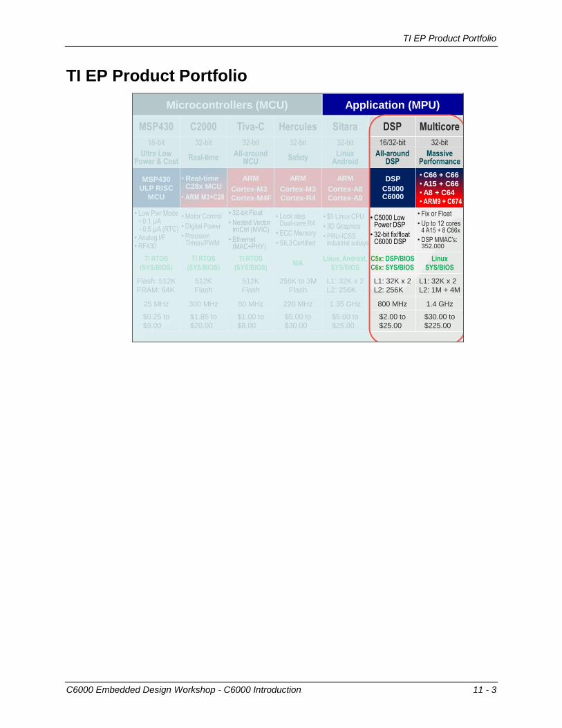
TI EP Product Portfolio
TI’s Embedded Processor PortfolioMicrocontrollers (MCU) Application (MPU)
MSP430 C2000 Tiva-C Hercules Sitara DSP Multicore
16-bit 32-bit 32-bit 32-bit 32-bit 16/32-bit 32-bit
Ultra Low Power & Cost
Real-timeAll-around
MCUSafety
LinuxAndroid
All-aroundDSP
Massive Performance
MSP430
ULP RISC
MCU
• Real-time C28x MCU
• ARM M3+C28
ARM
Cortex-M3
Cortex-M4F
ARM
Cortex-M3
Cortex-R4
ARM
Cortex-A8
Cortex-A9
DSP
C5000C6000
• C66 + C66
• A15 + C66
• A8 + C64
• ARM9 + C674
• Low Pwr Mode 0.1 µA 0.5 µA (RTC)
• Analog I/F• RF430
• Motor Control
• Digital Power
• Precision Timers/PWM
• 32-bit Float
• Nested Vector IntCtrl (NVIC)
• Ethernet (MAC+PHY)
• Lock step Dual-core R4
• ECC Memory
• SIL3Certified
• $5 Linux CPU
• 3D Graphics
• PRU-ICSS industrial subsys
• C5000 Low Power DSP
• 32-bit fix/float C6000 DSP
• Fix or Float
• Up to 12 cores 4 A15 + 8 C66x
• DSP MMAC’s: 352,000
TI RTOS
(SYS/BIOS)
TI RTOS
(SYS/BIOS)
TI RTOS
(SYS/BIOS)N/A
Linux, Android,
SYS/BIOS
C5x: DSP/BIOS
C6x: SYS/BIOS
Linux
SYS/BIOS
Flash: 512K
FRAM: 64K
512K
Flash
512K
Flash
256K to 3M
Flash
L1: 32K x 2
L2: 256K
L1: 32K x 2
L2: 256K
L1: 32K x 2
L2: 1M + 4M
25 MHz 300 MHz 80 MHz 220 MHz 1.35 GHz 800 MHz 1.4 GHz
$0.25 to
$9.00
$1.85 to
$20.00
$1.00 to
$8.00
$5.00 to
$30.00
$5.00 to
$25.00
$2.00 to
$25.00
$30.00 to
$225.00
DSP Core
11 - 4 C6000 Embedded Design Workshop - C6000 Introduction
DSP Core
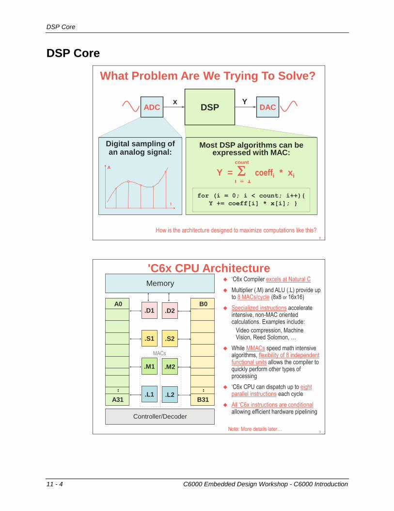
What Problem Are We Trying To Solve?
Digital sampling of an analog signal:
A
t
Most DSP algorithms can be expressed with MAC:
count
i = 1Y = coeffi * xi
for (i = 0; i < count; i++){
Y += coeff[i] * x[i]; }
DACx Y
ADC DSP
How is the architecture designed to maximize computations like this?8
'C6x CPU Architecture
Memory ‘C6x Compiler excels at Natural C
Multiplier (.M) and ALU (.L) provide up to 8 MACs/cycle (8x8 or 16x16)
Specialized instructions accelerate intensive, non-MAC oriented calculations. Examples include:
Video compression, Machine Vision, Reed Solomon, …
While MMACs speed math intensive algorithms, flexibility of 8 independent functional units allows the compiler to quickly perform other types of processing
‘C6x CPU can dispatch up to eight parallel instructions each cycle
All ‘C6x instructions are conditionalallowing efficient hardware pipelining
A0
A31
..
.S1
.D1
.L1
.S2
.M1 .M2
.D2
.L2
B0
B31
..
Controller/Decoder
MACs
Note: More details later…9
DSP Core
C6000 Embedded Design Workshop - C6000 Introduction 11 - 5
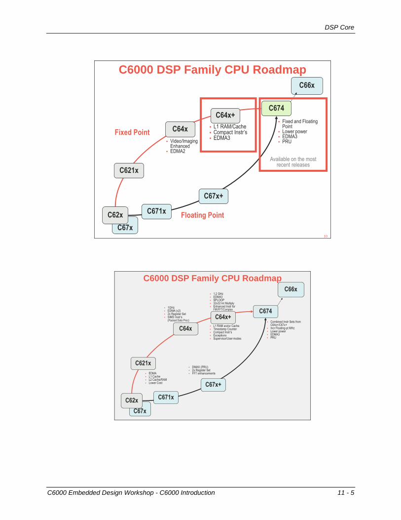
C66x
C67x
C6000 DSP Family CPU Roadmap
C62x
C64x+C674
C67x+
C64x
C671x
C621x
Floating Point
Fixed and Floating Point
Lower power EDMA3 PRU
L1 RAM/Cache Compact Instr’s EDMA3
Video/ImagingEnhanced
EDMA2
Fixed Point
Available on the most recent releases
10
C67x
C6000 DSP Family CPU Roadmap
C62x
C64x+
C66x
C674
C67x+
C64x
1GHz EDMA (v2) 2x Register Set SIMD Instr’s
(Packed Data Proc)
C671x
C621x
EDMA L1 Cache L2 Cache/RAM Lower Cost
DMAX (PRU) 2x Register Set FFT enhancements
1.2 GHz EDMA3 SPLOOP 32x32 Int Multiply Enhanced Instr for
FIR/FFT/Complex
Combined Instr Sets from C64x+/C67x+
Incr Floating-pt MHz Lower power EDMA3 PRU
L1 RAM and/or Cache Timestamp Counter Compact Instr’s Exceptions Supervisor/User modes
Devices & Documentation
11 - 6 C6000 Embedded Design Workshop - C6000 Introduction
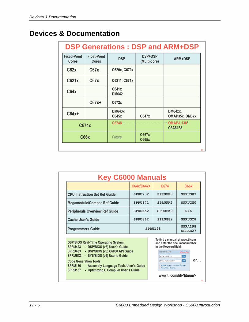
Devices & Documentation
DSP Generations : DSP and ARM+DSPFixed-Point
Cores
Float-Point
CoresDSP
DSP+DSP
(Multi-core)ARM+DSP
C62x C67x C620x, C670x
C621x C67x C6211, C671x
C64xC641x
DM642
C67x+ C672x
C64x+DM643x
C645x C647x
DM64xx,
OMAP35x, DM37x
C674xC6748 OMAP-L138*
C6A8168
C66x FutureC667x
C665x
13
DSP/BIOS Real-Time Operating System
SPRU423 - DSP/BIOS (v5) User’s Guide
SPRU403 - DSP/BIOS (v5) C6000 API Guide
SPRUEX3 - SYS/BIOS (v6) User’s Guide
Code Generation Tools
SPRU186 - Assembly Language Tools User’s Guide
SPRU187 - Optimizing C Compiler User’s Guide
Key C6000 ManualsC64x/C64x+ C674 C66x
CPU Instruction Set Ref Guide SPRU732 SPRUFE8 SPRUGH7
Megamodule/Corepac Ref Guide SPRU871 SPRUFK5 SPRUGW0
Peripherals Overview Ref Guide SPRUE52 SPRUFK9 N/A
Cache User’s Guide SPRU862 SPRUG82 SPRUGY8
Programmers Guide SPRU198 SPRA198
SPRAB27
To find a manual, at www.ti.comand enter the document number in the Keyword field:
or…
www.ti.com/lit/<litnum>14
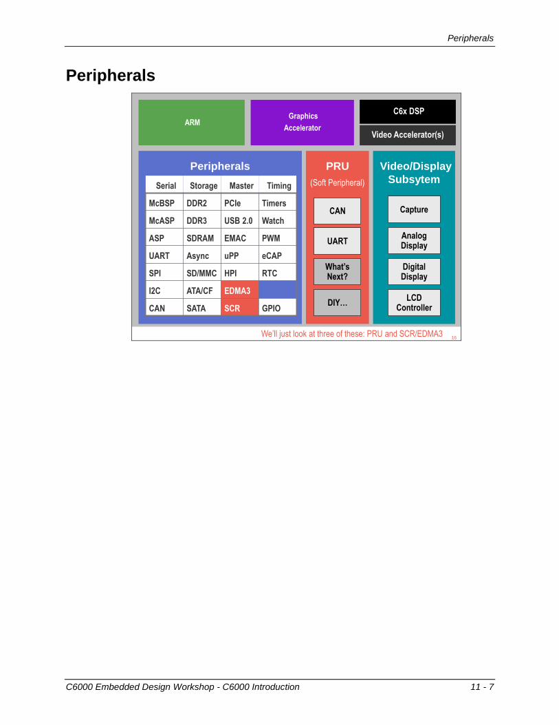
Peripherals
C6000 Embedded Design Workshop - C6000 Introduction 11 - 7
Peripherals
ARMGraphics
Accelerator
C6x DSP
Video Accelerator(s)
Peripherals Video/Display
Subsytem
PRU
(Soft Peripheral)
Capture
AnalogDisplay
DigitalDisplay
LCDController
What’s Next?
DIY…
Serial Storage Master Timing
McBSP DDR2 PCIe Timers
McASP DDR3 USB 2.0 Watch
ASP SDRAM EMAC PWM
UART Async uPP eCAP
SPI SD/MMC HPI RTC
I2C ATA/CF EDMA3
CAN SATA SCR GPIO
UART
CAN
We’ll just look at three of these: PRU and SCR/EDMA316
Peripherals
11 - 8 C6000 Embedded Design Workshop - C6000 Introduction
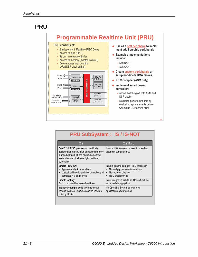
PRU
Programmable Realtime Unit (PRU)
Use as a soft peripheral to imple-ment add’l on-chip peripherals
Examples implementations include:
Soft UART
Soft CAN
Create custom peripherals or setup non-linear DMA moves.
No C compiler (ASM only)
Implement smart power controller:
Allows switching off both ARM and
DSP clocks
Maximize power down time by
evaluating system events before
waking up DSP and/or ARM
PRU consists of:
2 Independent, Realtime RISC Cores
Access to pins (GPIO)
Its own interrupt controller
Access to memory (master via SCR)
Device power mgmt control (ARM/DSP clock gating)
18
PRU SubSystem : IS / IS-NOT
Is IsNot
Dual 32bit RISC processor specifically
designed for manipulation of packed memory
mapped data structures and implementing
system features that have tight real time
constraints.
Is not a H/W accelerator used to speed up
algorithm computations.
Simple RISC ISA:
Approximately 40 instructions
Logical, arithmetic, and flow control ops all
complete in a single cycle
Is not a general purpose RISC processor:
No multiply hardware/instructions
No cache or pipeline
No C programming
Simple tooling:
Basic commandline assembler/linker
Is not integrated with CCS. Doesn’t include
advanced debug options
Includes example code to demonstrate
various features. Examples can be used as
building blocks.
No Operating System or high-level
application software stack
Peripherals
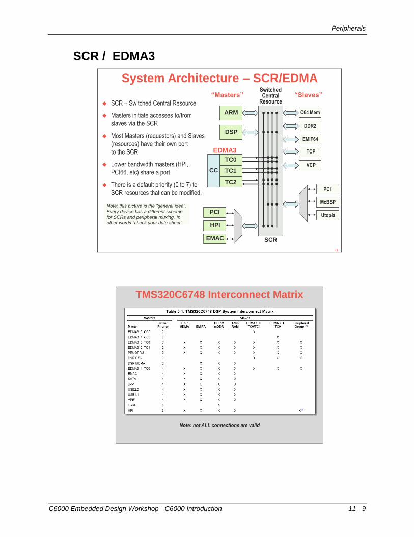
C6000 Embedded Design Workshop - C6000 Introduction 11 - 9
SCR / EDMA3
System Architecture – SCR/EDMA
ARM
DSP
TC0
TC1
TC2
CC
PCI
HPI
EMAC SCR
SwitchedCentral
Resource
C64 Mem
DDR2
EMIF64
TCP
VCP
PCI
McBSP
Utopia
“Masters” “Slaves”
SCR – Switched Central Resource
Masters initiate accesses to/from
slaves via the SCR
Most Masters (requestors) and Slaves
(resources) have their own port
to the SCR
Lower bandwidth masters (HPI,
PCI66, etc) share a port
There is a default priority (0 to 7) to
SCR resources that can be modified.
EDMA3
Note: this picture is the “general idea”.
Every device has a different scheme
for SCRs and peripheral muxing. In
other words “check your data sheet”.
21
TMS320C6748 Interconnect Matrix
Note: not ALL connections are valid
Peripherals
11 - 10 C6000 Embedded Design Workshop - C6000 Introduction
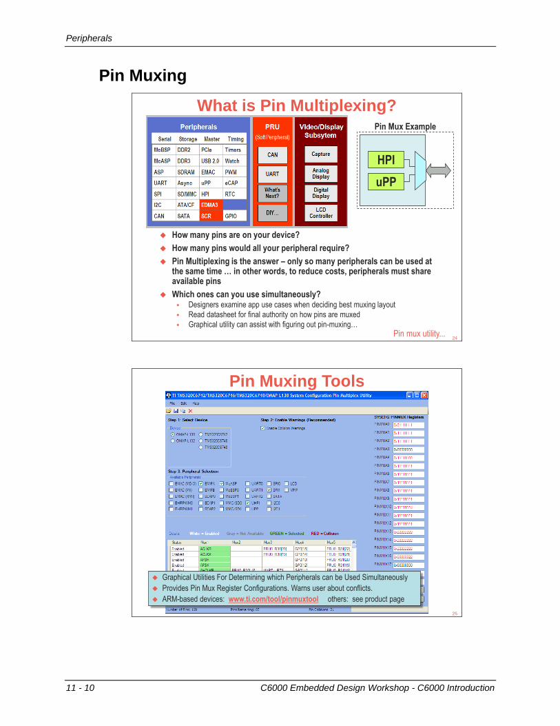
Pin Muxing
What is Pin Multiplexing?
How many pins are on your device?
How many pins would all your peripheral require?
Pin Multiplexing is the answer – only so many peripherals can be used at the same time … in other words, to reduce costs, peripherals must share available pins
Which ones can you use simultaneously? Designers examine app use cases when deciding best muxing layout
Read datasheet for final authority on how pins are muxed
Graphical utility can assist with figuring out pin-muxing…Pin mux utility...
HPI
uPP
Pin Mux Example
24
Pin Muxing Tools
Graphical Utilities For Determining which Peripherals can be Used Simultaneously
Provides Pin Mux Register Configurations. Warns user about conflicts.
ARM-based devices: www.ti.com/tool/pinmuxtool others: see product page
25
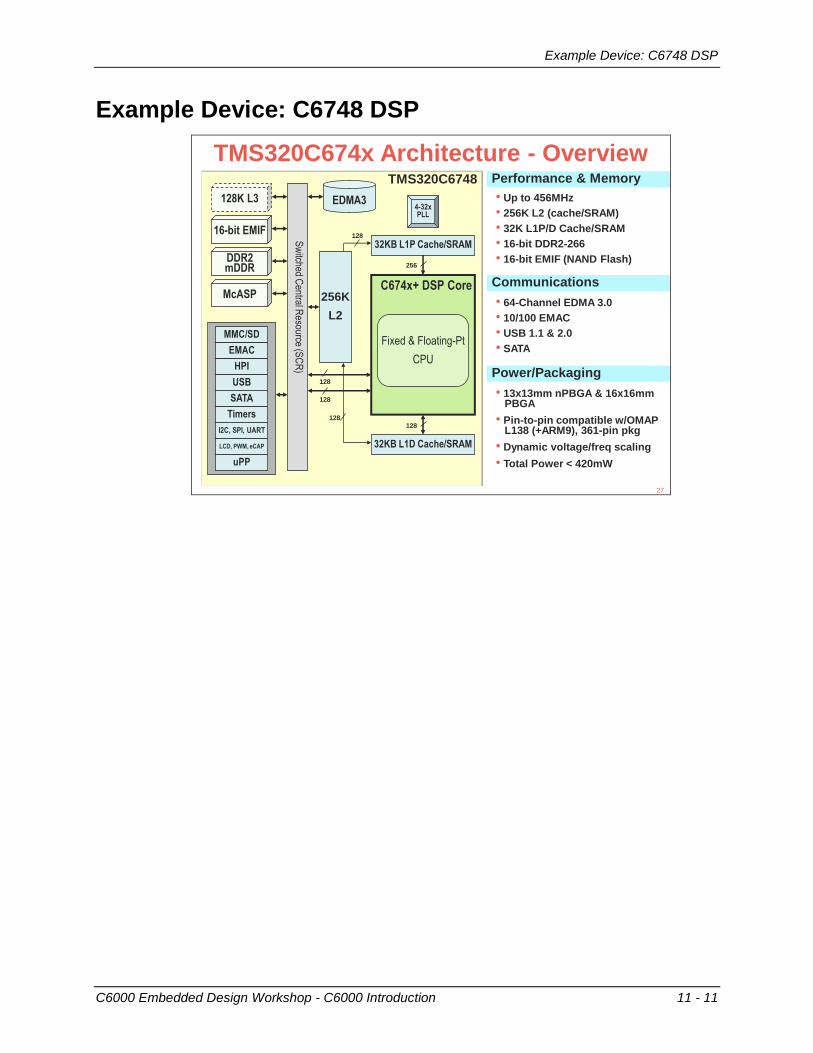
Example Device: C6748 DSP
C6000 Embedded Design Workshop - C6000 Introduction 11 - 11
Example Device: C6748 DSP
TMS320C674x Architecture - Overview
128K L3
16-bit EMIF
DDR2mDDR
McASP
MMC/SD
EMAC
HPI
SATA
I2C, SPI, UART
Sw
itched Central R
esource (SC
R)
256K
L2
EDMA3
C674x+ DSP Core
32KB L1P Cache/SRAM
32KB L1D Cache/SRAM
4-32xPLL
Performance & MemoryTMS320C6748
128
128
256
128
Communications
• Up to 456MHz
• 256K L2 (cache/SRAM)
• 32K L1P/D Cache/SRAM
• 16-bit DDR2-266
• 16-bit EMIF (NAND Flash)
• 64-Channel EDMA 3.0
• 10/100 EMAC
• USB 1.1 & 2.0
• SATA
Power/Packaging
• 13x13mm nPBGA & 16x16mmPBGA
• Pin-to-pin compatible w/OMAPL138 (+ARM9), 361-pin pkg
• Dynamic voltage/freq scaling
• Total Power < 420mW
128
128
USB
Timers
LCD, PWM, eCAP
uPP
Fixed & Floating-Pt
CPU
27
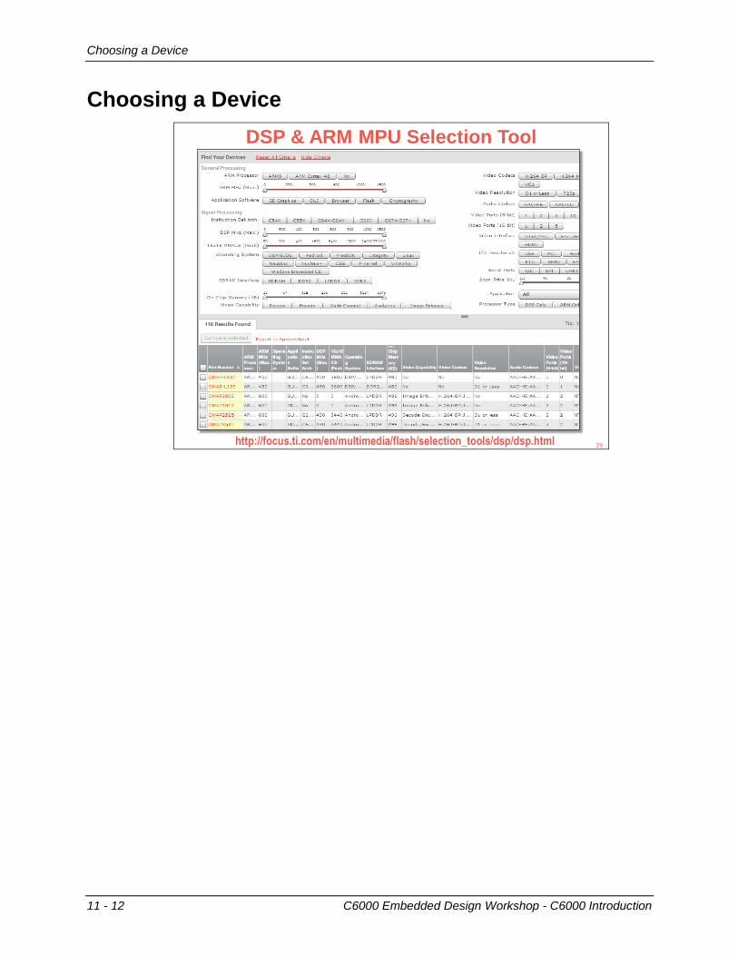
Choosing a Device
11 - 12 C6000 Embedded Design Workshop - C6000 Introduction
Choosing a Device
DSP & ARM MPU Selection Tool
http://focus.ti.com/en/multimedia/flash/selection_tools/dsp/dsp.html 29
C6000 Arch “Catchup”
C6000 Embedded Design Workshop - C6000 Introduction 11 - 13
C6000 Arch “Catchup”
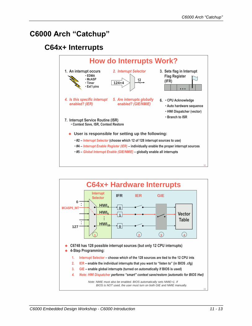
C64x+ Interrupts
How do Interrupts Work?
1. An interrupt occurs• EDMA• McASP• Timer• Ext’l pins
2. Interrupt Selector
124+412
3. Sets flag in Interrupt
Flag Register
(IFR)
…
4. Is this specific interruptenabled? (IER)
5. Are interrupts globallyenabled? (GIE/NMIE)
6. • CPU Acknowledge
• Auto hardware sequence
• HWI Dispatcher (vector)
• Branch to ISR7. Interrupt Service Routine (ISR)
• Context Save, ISR, Context Restore
User is responsible for setting up the following:
• #2 – Interrupt Selector (choose which 12 of 128 interrupt sources to use)
• #4 – Interrupt Enable Register (IER) – individually enable the proper interrupt sources
• #5 – Global Interrupt Enable (GIE/NMIE) – globally enable all interrupts
32
C64x+ Hardware Interrupts
C6748 has 128 possible interrupt sources (but only 12 CPU interrupts)
4-Step Programming:
Interrupt
Selector0 .
.MCASP0_INT
.
.127
0HWI4
1HWI5
0HWI15
...
IFR IER GIE
Vector
Table
1. Interrupt Selector – choose which of the 128 sources are tied to the 12 CPU ints
2. IER – enable the individual interrupts that you want to “listen to” (in BIOS .cfg)
3. GIE – enable global interrupts (turned on automatically if BIOS is used)
4. Note: HWI Dispatcher performs “smart” context save/restore (automatic for BIOS Hwi)
1 2 3 4
Note: NMIE must also be enabled. BIOS automatically sets NMIE=1. If
BIOS is NOT used, the user must turn on both GIE and NMIE manually.
33
C6000 Arch “Catchup”
11 - 14 C6000 Embedded Design Workshop - C6000 Introduction
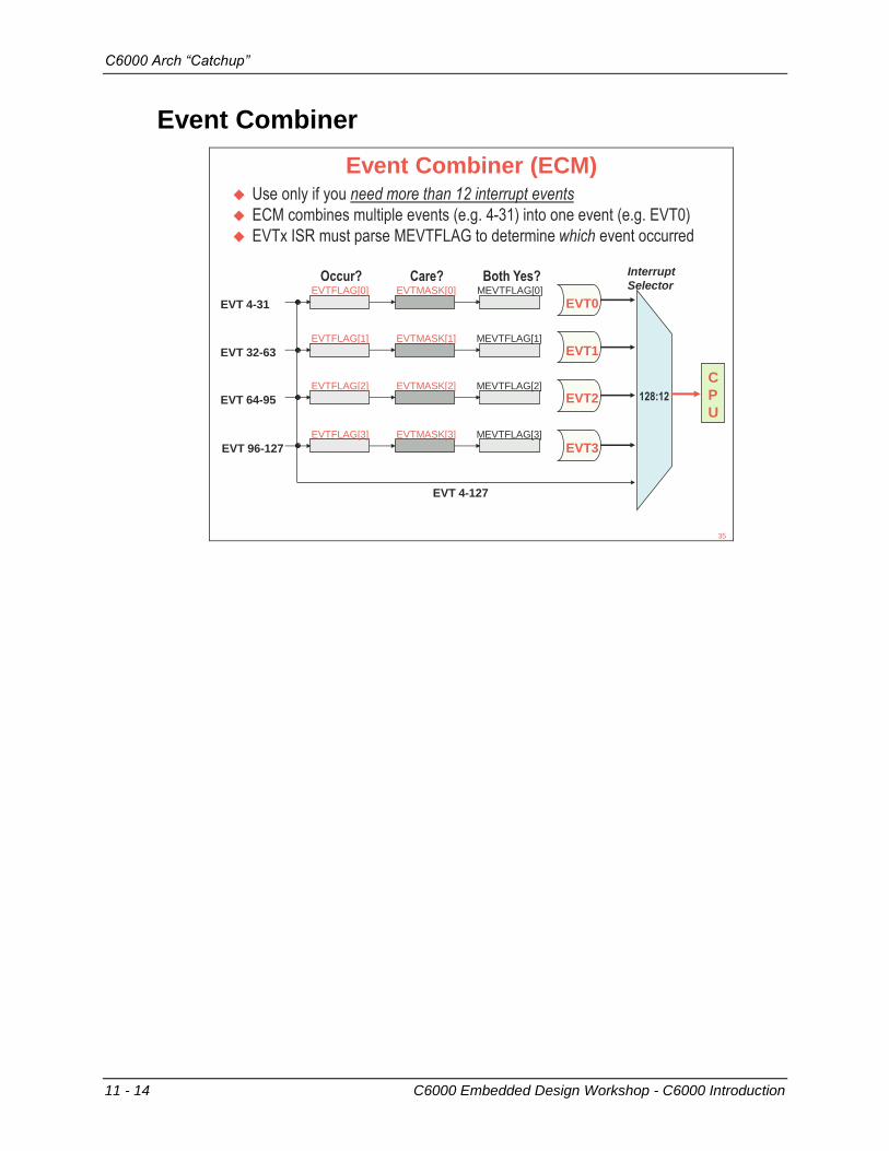
Event Combiner
Event Combiner (ECM)
EVT 4-31
EVTFLAG[0]
Interrupt
Selector
C
P
U128:12
EVT 32-63
EVTFLAG[1]
EVT 64-95
EVTFLAG[2]
EVT 96-127
EVTFLAG[3]
EVTMASK[0]
EVTMASK[1]
EVTMASK[2]
EVTMASK[3]
MEVTFLAG[0]
MEVTFLAG[1]
MEVTFLAG[2]
MEVTFLAG[3]
EVT0
EVT1
EVT2
EVT3
EVT 4-127
Occur? Care? Both Yes?
Use only if you need more than 12 interrupt events
ECM combines multiple events (e.g. 4-31) into one event (e.g. EVT0)
EVTx ISR must parse MEVTFLAG to determine which event occurred
35
C6000 Arch “Catchup”
C6000 Embedded Design Workshop - C6000 Introduction 11 - 15
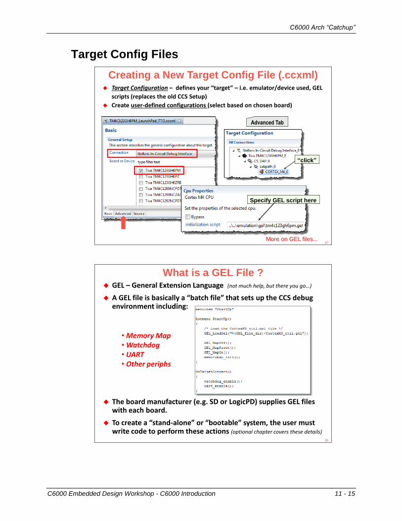
Target Config Files
Creating a New Target Config File (.ccxml) Target Configuration – defines your “target” – i.e. emulator/device used, GEL
scripts (replaces the old CCS Setup)
Create user-defined configurations (select based on chosen board)
“click”
Advanced Tab
More on GEL files...
Specify GEL script here
37
What is a GEL File ? GEL – General Extension Language (not much help, but there you go…)
A GEL file is basically a “batch file” that sets up the CCS debugenvironment including:
• Memory Map• Watchdog• UART• Other periphs
The board manufacturer (e.g. SD or LogicPD) supplies GEL fileswith each board.
To create a “stand-alone” or “bootable” system, the user mustwrite code to perform these actions (optional chapter covers these details)
38
C6000 Arch “Catchup”
11 - 16 C6000 Embedded Design Workshop - C6000 Introduction
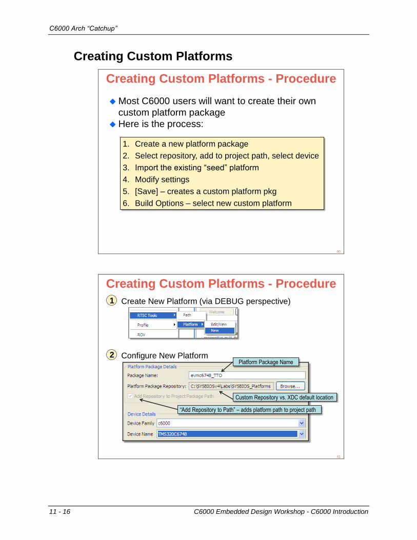
Creating Custom Platforms
Creating Custom Platforms - Procedure
Most C6000 users will want to create their own
custom platform package
Here is the process:
1. Create a new platform package
2. Select repository, add to project path, select device
3. Import the existing “seed” platform
4. Modify settings
5. [Save] – creates a custom platform pkg
6. Build Options – select new custom platform
40
Creating Custom Platforms - Procedure
1 Create New Platform (via DEBUG perspective)
2 Configure New Platform
“Add Repository to Path” – adds platform path to project path
Custom Repository vs. XDC default location
Platform Package Name
41
C6000 Arch “Catchup”
C6000 Embedded Design Workshop - C6000 Introduction 11 - 17
Creating Custom Platforms - Procedure
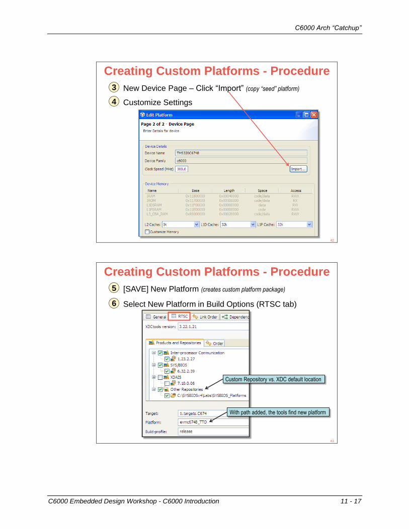
3 New Device Page – Click “Import” (copy “seed” platform)
4 Customize Settings
42
Creating Custom Platforms - Procedure
5 [SAVE] New Platform (creates custom platform package)
6 Select New Platform in Build Options (RTSC tab)
Custom Repository vs. XDC default location
With path added, the tools find new platform
43

C6000 Arch “Catchup”
11 - 18 C6000 Embedded Design Workshop - C6000 Introduction
*** this page is blank for absolutely no reason ***
Quiz
C6000 Embedded Design Workshop - C6000 Introduction 11 - 19
Quiz
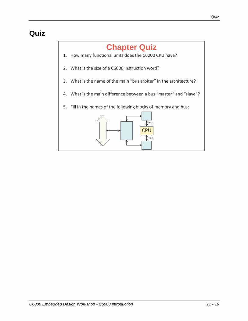
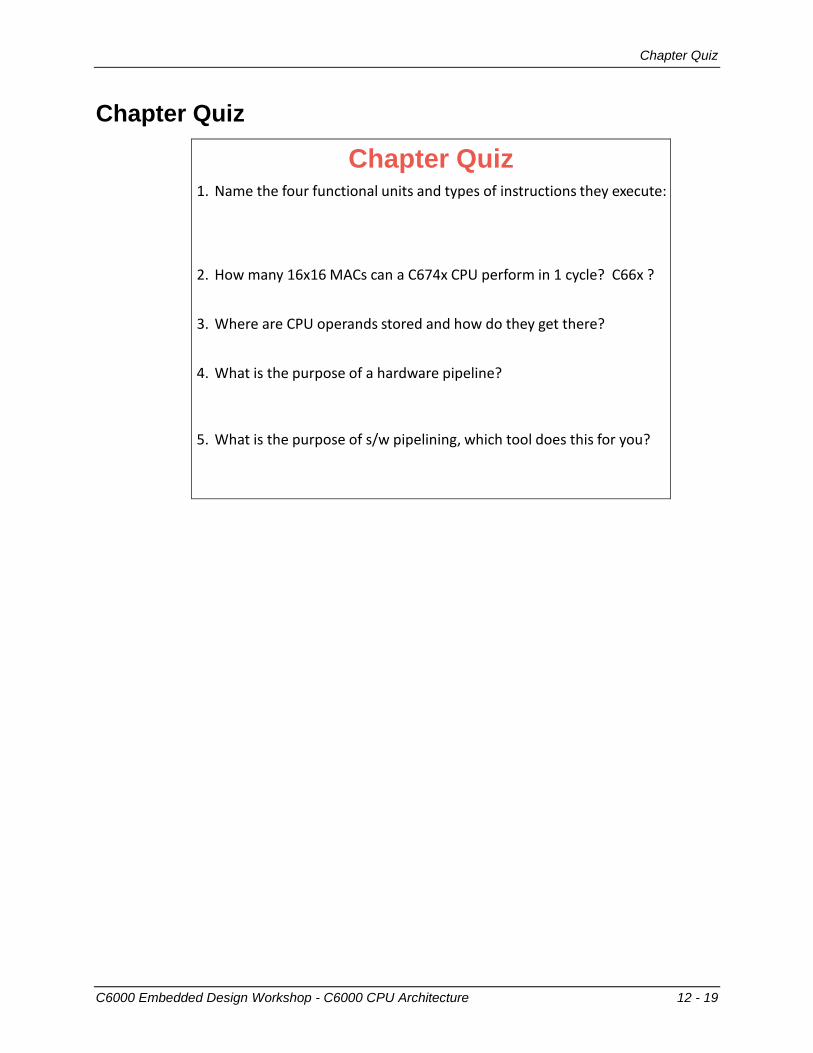
Chapter Quiz
CPU
256
128
1. How many functional units does the C6000 CPU have?
2. What is the size of a C6000 instruction word?
3. What is the name of the main “bus arbiter” in the architecture?
4. What is the main difference between a bus “master” and “slave”?
5. Fill in the names of the following blocks of memory and bus:
Quiz
11 - 20 C6000 Embedded Design Workshop - C6000 Introduction
Quiz - Answers
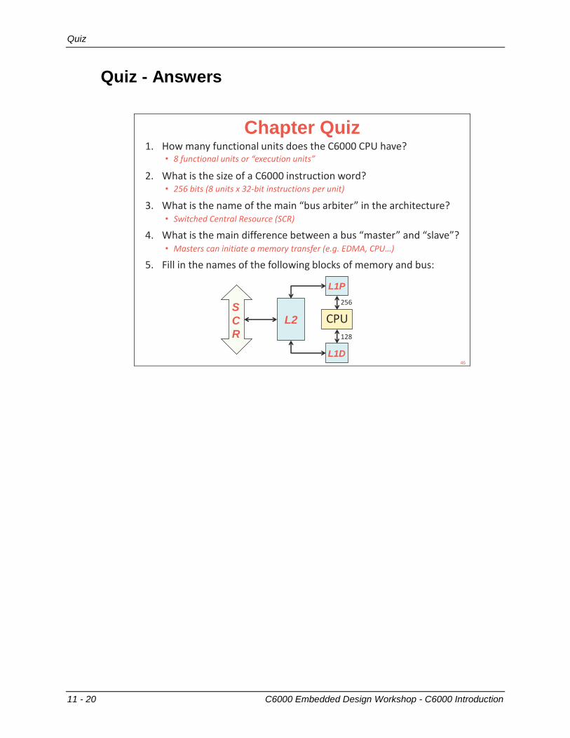
Chapter Quiz
• 8 functional units or “execution units”
• 256 bits (8 units x 32-bit instructions per unit)
• Switched Central Resource (SCR)
• Masters can initiate a memory transfer (e.g. EDMA, CPU…)
CPU
256
128
L1P
L1D
L2S
C
R
1. How many functional units does the C6000 CPU have?
2. What is the size of a C6000 instruction word?
3. What is the name of the main “bus arbiter” in the architecture?
4. What is the main difference between a bus “master” and “slave”?
5. Fill in the names of the following blocks of memory and bus:
46
Using Double Buffers
C6000 Embedded Design Workshop - C6000 Introduction 11 - 21
Using Double Buffers
Hwi
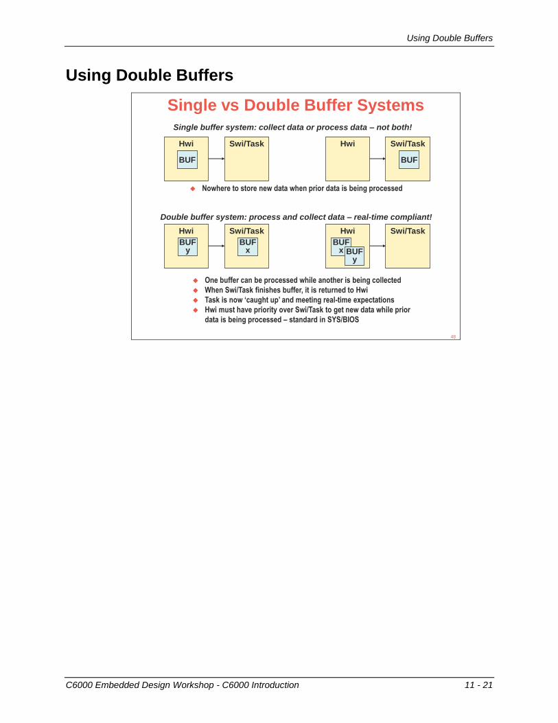
Single vs Double Buffer Systems
BUF
Swi/Task Hwi Swi/Task
BUF
Single buffer system: collect data or process data – not both!
Hwi Swi/Task Hwi Swi/Task
BUFx
Double buffer system: process and collect data – real-time compliant!
BUFy
BUFx BUF
y
One buffer can be processed while another is being collected
When Swi/Task finishes buffer, it is returned to Hwi
Task is now ‘caught up’ and meeting real-time expectations
Hwi must have priority over Swi/Task to get new data while prior
data is being processed – standard in SYS/BIOS
Nowhere to store new data when prior data is being processed
48
Using Double Buffers
11 - 22 C6000 Embedded Design Workshop - C6000 Introduction
*** HTTP ERROR 404 – PAGE NOT FOUND ***
Lab 11: An Hwi-Based Audio System
C6000 Embedded Design Workshop - C6000 Introduction 11 - 23
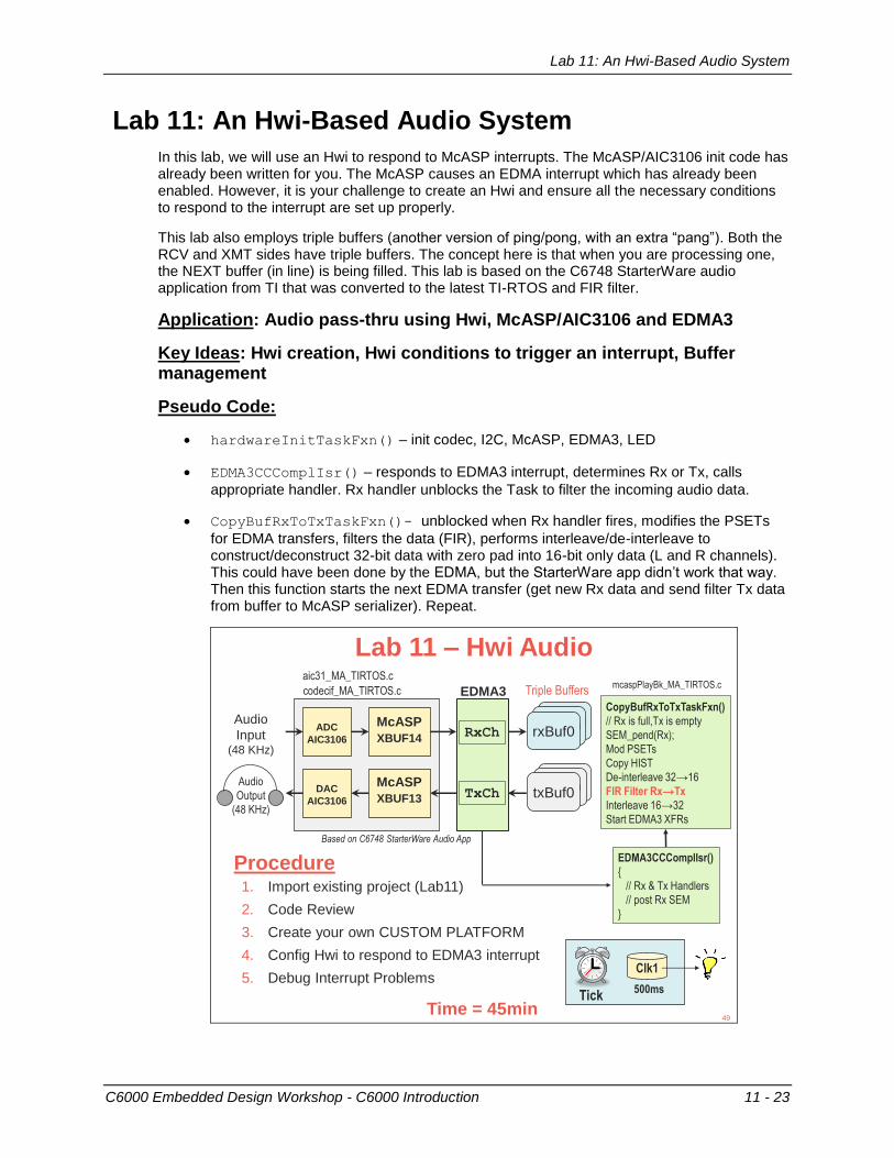
Lab 11: An Hwi-Based Audio System
In this lab, we will use an Hwi to respond to McASP interrupts. The McASP/AIC3106 init code has already been written for you. The McASP causes an EDMA interrupt which has already been enabled. However, it is your challenge to create an Hwi and ensure all the necessary conditions to respond to the interrupt are set up properly.
This lab also employs triple buffers (another version of ping/pong, with an extra “pang”). Both the RCV and XMT sides have triple buffers. The concept here is that when you are processing one, the NEXT buffer (in line) is being filled. This lab is based on the C6748 StarterWare audio application from TI that was converted to the latest TI-RTOS and FIR filter.
Application: Audio pass-thru using Hwi, McASP/AIC3106 and EDMA3
Key Ideas: Hwi creation, Hwi conditions to trigger an interrupt, Buffer management
Pseudo Code:
hardwareInitTaskFxn() – init codec, I2C, McASP, EDMA3, LED
EDMA3CCComplIsr() – responds to EDMA3 interrupt, determines Rx or Tx, calls
appropriate handler. Rx handler unblocks the Task to filter the incoming audio data.
CopyBufRxToTxTaskFxn()- unblocked when Rx handler fires, modifies the PSETs
for EDMA transfers, filters the data (FIR), performs interleave/de-interleave to construct/deconstruct 32-bit data with zero pad into 16-bit only data (L and R channels). This could have been done by the EDMA, but the StarterWare app didn’t work that way. Then this function starts the next EDMA transfer (get new Rx data and send filter Tx data from buffer to McASP serializer). Repeat.
Audio
Output
(48 KHz)
Lab 11 – Hwi Audio
ADC
AIC3106
Audio
Input (48 KHz)
McASP
XBUF14
DAC
AIC3106
McASP
XBUF13
1. Import existing project (Lab11)
2. Code Review
3. Create your own CUSTOM PLATFORM
4. Config Hwi to respond to EDMA3 interrupt
5. Debug Interrupt Problems
aic31_MA_TIRTOS.c
codecif_MA_TIRTOS.cmcaspPlayBk_MA_TIRTOS.c
rxBuf0rxBuf0rxBuf0
Triple Buffers
Time = 45min
Procedure
49
txBuf0txBuf0txBuf0
EDMA3
RxCh
TxCh
CopyBufRxToTxTaskFxn()
// Rx is full,Tx is empty
SEM_pend(Rx);
Mod PSETs
Copy HIST
De-interleave 32→16
FIR Filter Rx→Tx
Interleave 16→32
Start EDMA3 XFRs
EDMA3CCComplIsr()
{
// Rx & Tx Handlers
// post Rx SEM
}
Based on C6748 StarterWare Audio App
Clk1
Tick500ms
Lab 11 – Procedure
11 - 24 C6000 Embedded Design Workshop - C6000 Introduction
Lab 11 – Procedure
If you can’t remember how to perform some of these steps, please refer back to the previous labs for help. Or, if you really get stuck, ask your neighbor. If you AND your neighbor get stuck, then ask the instructor (who is probably doing absolutely NOTHING important) for help.
Import Existing Project
1. Close ALL open projects and files and then open CCS.
2. Import Lab11 project.
► As before, import the archived starter project from:
C:\TI-RTOS\C6000\Labs\Lab_11\
This starter file contains all the starting source files for the audio project including the setup code for the A/D and D/A on the C6748 LCDK (or OMAP-L138 LCDK). It also has UIA activated but this won’t be used until the next lab.
3. Check the Properties to ensure you are using the latest XDC, BIOS and UIA.
For every imported project in this workshop, ALWAYS check to make sure the latest tools (XDC, BIOS and UIA) are being used. The author created these projects at time “x” and you may have updated the tools on your student PC at “x+1” – some time later. The author used the tools available at time “x” to create the starter projects and solutions which may or may not match YOUR current set of tools.
Therefore, you may be importing a project that is NOT using the latest versions of the tools (XDC, BIOS, UIA) or the compiler.
► Check ALL settings for the Properties of the project (XDC, BIOS, UIA) and the compiler and update the imported project to the latest tools before moving on and save all settings.
Lab 11 – Procedure
C6000 Embedded Design Workshop - C6000 Introduction 11 - 25
Application (FIR Audio) Overview
4. Let’s review what this audio pass-thru code is doing.
As discussed in the lab description, this application is based on the C6748 StarterWare audio app which can be downloaded from:
http://www.ti.com/tool/starterware-c6dsp
Once downloaded, the original application can be obtained by importing the project located at:
[STARTERWARE_INSTALL_PATH]\build\c674x\cgt_ccs\c6748\lcdkC6748\mcasp
The author then modified the code to make it TI-RTOS compliant and added a FIR filter of the audio data that will be optimized in a future lab.
The best way to understand the process is via I-P-O:
Input (RCV) – each analog audio sample from the audio INPUT port of the LCDK (top
stereo audio jack) is converted by the A/D and sent to the McASP port on the C6748. For
each sample, the McASP generates an EDMA3 event which fills up the rxBuf[0-2] buffer.
When the rxBuf is full, the EDMA generates an interrupt to the CPU. In the ISR, Rx and
Tx are handled separately. Assuming the Rx and Tx are running at the same frequency,
only Rx unblocks the processing Task to filter the audio data…
Process – Assuming at this point that the next Rx buffer is full and the next Tx buffer is
empty, it is time to process the data. A simple pass-thru would just copy Rx to Tx which is
what the original StarterWare application did. However, the author modified that code to
perform an FIR filter. The original code peformed 32-bit reads and writes with the upper
16 bits of each “sample” padded with zeroes. An off the shelf FIR filter can’t process this
type of data. It needs to be channelized (L and R), converted to 16 bits and remove the
zeroes. So, a de-interleave routine is done first to create a new local Rx buffer. That
buffer is then filtered to create a new local Tx buffer. When that process is complete, an
interleave routine is done to put the data back into a zero-padded 32-bit format which the
EDMA copies to the McASP (Tx) serializer…
Output (XMT) – When the EDMA Tx transfer starts, it copies one sample at a time to the
McASP Tx serializer. When a buffer full of samples have been transferred, the Tx EDMA
channel interrupts the CPU to say “done”. Again, assuming that the Rx and Tx transfers
are synced, the Rx interrupt would then unblock the processing Task above.
Several source files are needed to create this application. Let’s explore those briefly…
Lab 11 – Procedure
11 - 26 C6000 Embedded Design Workshop - C6000 Introduction
Source Code Overview
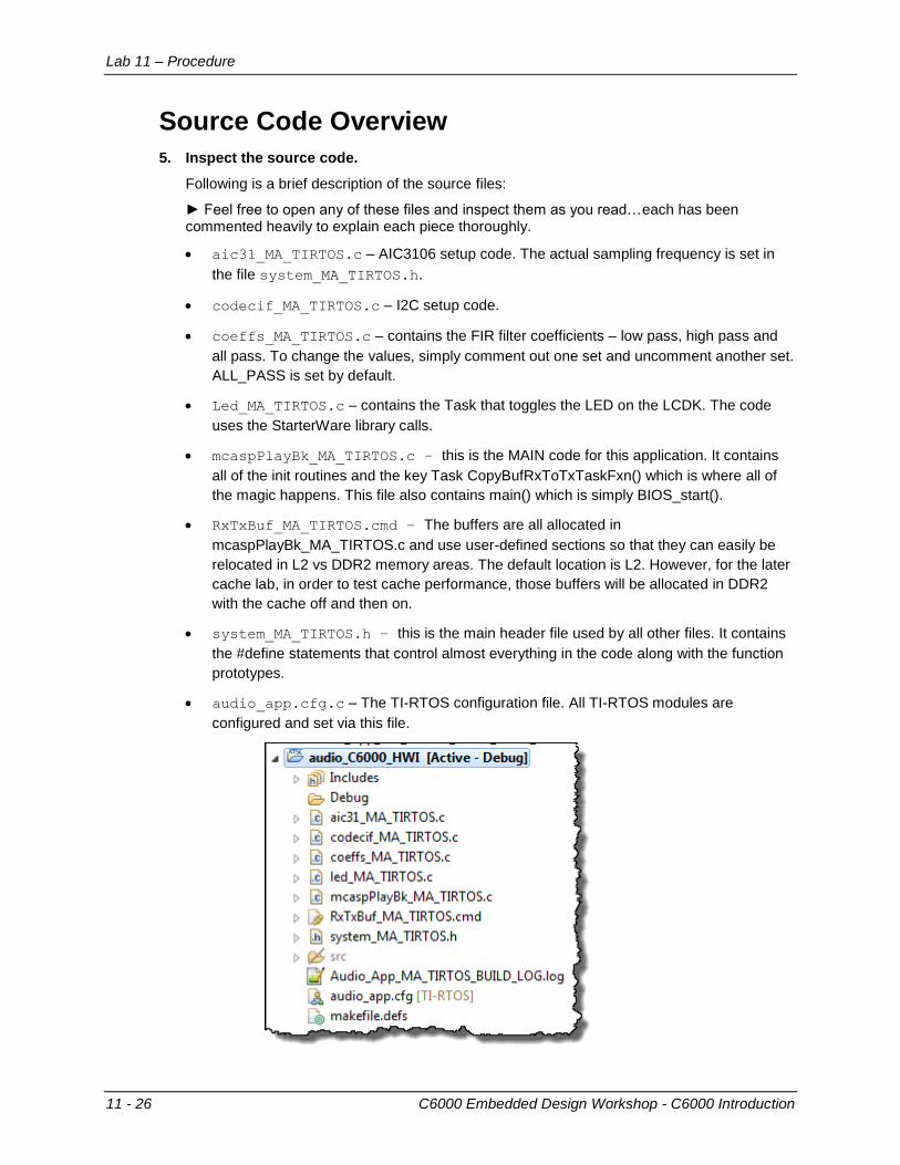
5. Inspect the source code.
Following is a brief description of the source files:
► Feel free to open any of these files and inspect them as you read…each has been commented heavily to explain each piece thoroughly.
aic31_MA_TIRTOS.c – AIC3106 setup code. The actual sampling frequency is set in
the file system_MA_TIRTOS.h.
codecif_MA_TIRTOS.c – I2C setup code.
coeffs_MA_TIRTOS.c – contains the FIR filter coefficients – low pass, high pass and
all pass. To change the values, simply comment out one set and uncomment another set.
ALL_PASS is set by default.
Led_MA_TIRTOS.c – contains the Task that toggles the LED on the LCDK. The code
uses the StarterWare library calls.
mcaspPlayBk_MA_TIRTOS.c – this is the MAIN code for this application. It contains
all of the init routines and the key Task CopyBufRxToTxTaskFxn() which is where all of
the magic happens. This file also contains main() which is simply BIOS_start().
RxTxBuf_MA_TIRTOS.cmd – The buffers are all allocated in
mcaspPlayBk_MA_TIRTOS.c and use user-defined sections so that they can easily be
relocated in L2 vs DDR2 memory areas. The default location is L2. However, for the later
cache lab, in order to test cache performance, those buffers will be allocated in DDR2
with the cache off and then on.
system_MA_TIRTOS.h – this is the main header file used by all other files. It contains
the #define statements that control almost everything in the code along with the function
prototypes.
audio_app.cfg.c – The TI-RTOS configuration file. All TI-RTOS modules are
configured and set via this file.
Lab 11 – Procedure
C6000 Embedded Design Workshop - C6000 Introduction 11 - 27
Add Hwi to the Project
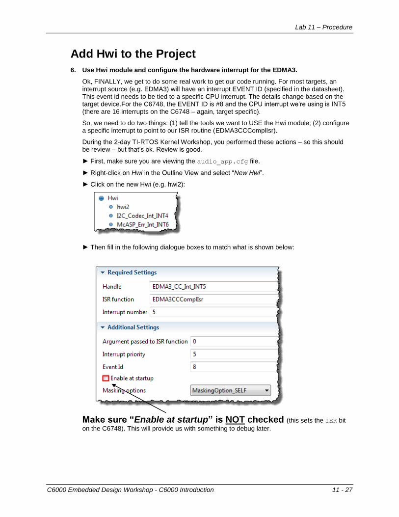
6. Use Hwi module and configure the hardware interrupt for the EDMA3.
Ok, FINALLY, we get to do some real work to get our code running. For most targets, an interrupt source (e.g. EDMA3) will have an interrupt EVENT ID (specified in the datasheet). This event id needs to be tied to a specific CPU interrupt. The details change based on the target device.For the C6748, the EVENT ID is #8 and the CPU interrupt we’re using is INT5 (there are 16 interrupts on the C6748 – again, target specific).
So, we need to do two things: (1) tell the tools we want to USE the Hwi module; (2) configure a specific interrupt to point to our ISR routine (EDMA3CCComplIsr).
During the 2-day TI-RTOS Kernel Workshop, you performed these actions – so this should be review – but that’s ok. Review is good.
► First, make sure you are viewing the audio_app.cfg file.
► Right-click on Hwi in the Outline View and select “New Hwi”.
► Click on the new Hwi (e.g. hwi2):
► Then fill in the following dialogue boxes to match what is shown below:
Make sure “Enable at startup” is NOT checked (this sets the IER bit
on the C6748). This will provide us with something to debug later.
Lab 11 – Procedure
11 - 28 C6000 Embedded Design Workshop - C6000 Introduction
Optional – OMAP-L138 LCDK Users ONLY
C6748 LCDK users know how to build, load and run these labs – they did this multiple times during the TI-RTOS workshop. However, because this workshop supports either board, there are a few steps that an OMAP-L138 user needs to perform that are DIFFERENT than a C6748 user.
The following information will help users of the OMAP-L138 LCDK get these labs to work properly.
First, the devices are very similar. For build, you can target either the C6748 LCDK or the OMAP-L138 LCDK in (right-click on the project) Properties→General. The author chose to simplify things
and just keep the C6748 LCDK as the target. That works fine.
Second, the OMAP device contains an ARM9 CPU that must be powered up FIRST before the DSP (C674x). So, OMAP-L138 users must do two things in addition to the C6748 LCDK users:
Use a different target configuration file
Connect to the ARM9 first, followed by the DSP and then load the .out file to the DSP.
Using a different target configuration file
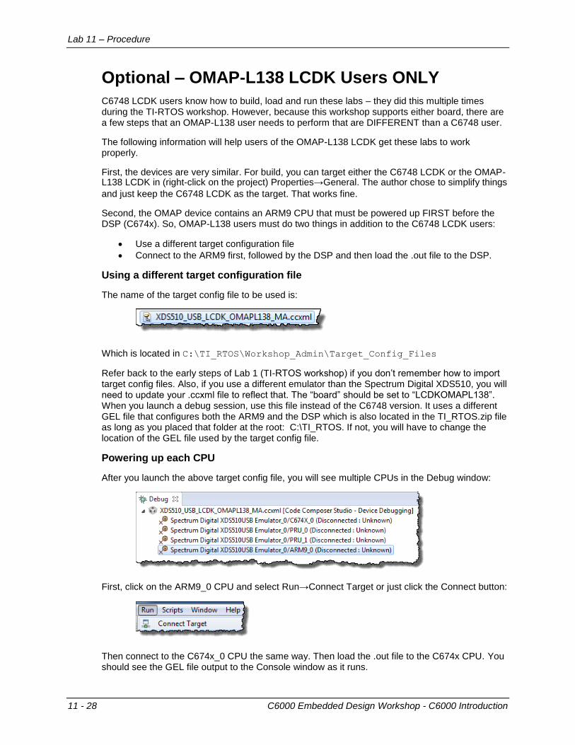
The name of the target config file to be used is:
Which is located in C:\TI_RTOS\Workshop_Admin\Target_Config_Files
Refer back to the early steps of Lab 1 (TI-RTOS workshop) if you don’t remember how to import target config files. Also, if you use a different emulator than the Spectrum Digital XDS510, you will need to update your .ccxml file to reflect that. The “board” should be set to “LCDKOMAPL138”. When you launch a debug session, use this file instead of the C6748 version. It uses a different GEL file that configures both the ARM9 and the DSP which is also located in the TI_RTOS.zip file as long as you placed that folder at the root: C:\TI_RTOS. If not, you will have to change the location of the GEL file used by the target config file.
Powering up each CPU
After you launch the above target config file, you will see multiple CPUs in the Debug window:
First, click on the ARM9_0 CPU and select Run→Connect Target or just click the Connect button:
Then connect to the C674x_0 CPU the same way. Then load the .out file to the C674x CPU. You should see the GEL file output to the Console window as it runs.
Lab 11 – Procedure
C6000 Embedded Design Workshop - C6000 Introduction 11 - 29
Build, Load, Run.
7. Build, load and run the audio FIR filter application.
► Before you Run, make sure audio is playing into the board and your headphones are set up so you can hear the audio. The TOP jack is INPUT (from your PC) and the BOTTOM jack is OUTPUT (to your headphone).
► Also, make sure that Windows Media Player is set to REPEAT forever. If the music stops (the input is air), and you click Run, you might think there is a problem with your code. Nope, there is no music playing.
► Build and fix any errors. After a successful build, load the .out file to your target board.
OMAP-L138 LCDK USERS ONLY: Remember, OMAP-L138 LCDK users need to connect to the ARM9 first, then connect to the C674x CPU second. Then, make sure the C674x CPU is highlighted and LOAD the .out file to that CPU.
► Once the program is loaded, click Run.
Do you hear audio? If not, it’s debug time – it SHOULD NOT be working (by design). One quick tip for debug is to place a breakpoint in the EDMA3CCComplIsr() routine (located in
mcaspPlayBk_MA_TIRTOS.c) and see if the program stops there. If not, no interrupt is
being generated. Move on to the next steps to debug the problem…
Hint: The StarterWare application has a unique “send zeroes if McASP Xmt underruns” feature. Normally, the McASP on the C6748 cannot be restarted after a halt – i.e. you can’t just hit halt, then Run. However, in this application, if a halt occurs and underruns the XMT side of the McASP, the application continues to send ZEROES to the output to keep it alive vs simply dying. This is a nice feature. You may hear “static” when you halt, but you can simply click Play again to keep running.
Debug Interrupt Problem
As we already know, we decided early on to NOT enable the IER bit in the static configuration of the Hwi. Ok. But debugging interrupt problems is a crucial skill. The next few steps walk you through HOW to do this. You may not know WHERE your interrupt problem occurred, so using these brief debug skills may help in the future.
8. Pause for a moment to reflect on the “dominos” in the interrupt game:
An interrupt must occur (McASP event to EDMA3 must be set along with the EDMA3 options register for each channel must be configured to interrupt the CPU). Our init code does this already.
The individual interrupt must be enabled (IER, BITx) – which is NOT enabled right now.
Global Interrupts must be turned on (GIE = 1, handled by TI-RTOS)
HWI Dispatcher must be used to provide proper context save/restore (automatic when using TI-RTOS to manage interrupts)
Keep this all in mind as you do the following steps…
Lab 11 – Procedure
11 - 30 C6000 Embedded Design Workshop - C6000 Introduction
9. EDMA3CC interrupt firing – IFR bit set?
If your application is still running, halt it.
The EDMA3 Channel Controller (CC) interrupt is set to fire properly, but is it setting the IFR
bit? You configured HWI_INT5, so that would be a “1” in bit 5 (IF5) of the IFR.
► Go there now (View → Registers → Core Registers).
► Look down the list to find the IFR and IER – the two of most interest at the moment.
(author note: could it have been set, then auto-cleared already?). You can also DISABLE IERbit (as it is already in the CFG file), build/run, and THEN look at IFR (this is a nice trick). So, if you have the IER set and the interrupt fires (IFR is set), it gets cleared automatically by hardware. So turning off IER allows us to see the IFR bit being set.
Expand “IFR” and look for IF5 (because the EDMA3 interrupt is tied to CPU INT #5)…
Write your debug “checkmarks” here:
IFR bit set? □ Yes □ No
10. Is the IER bit set?
Interrupts must be individually enabled. When you look at IER bit 5, is it set to “1”? Probably
NOT because we didn’t check that “Enable at Start” checkbox.
► Open up the config for HWI_INT5 and check the proper checkbox. Then, hit build and your code will build and load automatically regardless of which perspective you are in. Run. Do you hear audio playing now? The “all pass” filter coefficients are set by default so your music should sound normal.
► Halt the CPU. Is the IER bit (IE05) bit set?
IER bit set? □ Yes □ No
So let’s check one more thing…
11. Is GIE set?
The Global Interrupt Enable (GIE) Bit is located in the CPU’s CSR register. TI-RTOS turns this
on automatically and then manages it as part of the O/S. So, no need to check on this but do FIND this bit in the CSR register so you know where it is…
GIE bit set? □ Yes □ No
Hint: If you create a project that does NOT use SYS/BIOS (or TI-RTOS), it is the responsibility
of the user to not only turn on GIE, but also NMIE in the CSR register. Otherwise, NO
interrupts will be recognized. Ever. Did I say ever?
Lab 11 – Procedure
C6000 Embedded Design Workshop - C6000 Introduction 11 - 31
Using the Profiler Clock
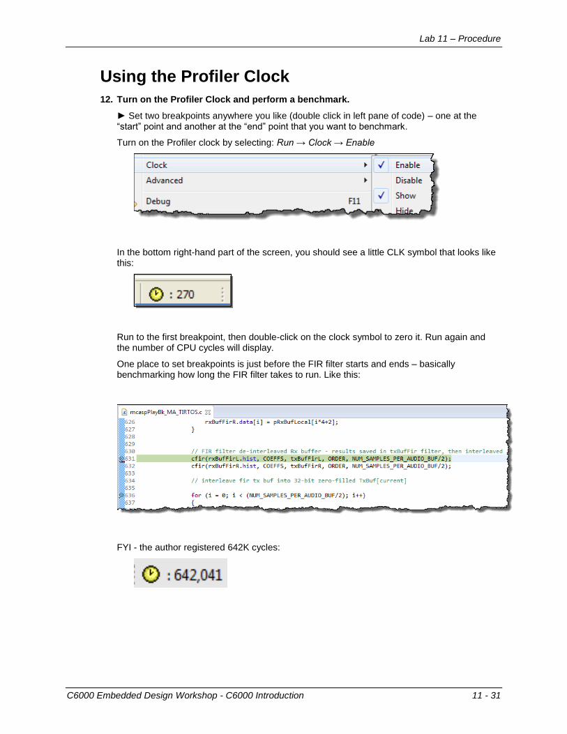
12. Turn on the Profiler Clock and perform a benchmark.
► Set two breakpoints anywhere you like (double click in left pane of code) – one at the “start” point and another at the “end” point that you want to benchmark.
Turn on the Profiler clock by selecting: Run → Clock → Enable
In the bottom right-hand part of the screen, you should see a little CLK symbol that looks like this:
Run to the first breakpoint, then double-click on the clock symbol to zero it. Run again and the number of CPU cycles will display.
One place to set breakpoints is just before the FIR filter starts and ends – basically benchmarking how long the FIR filter takes to run. Like this:
FYI - the author registered 642K cycles:
Lab 11 – Procedure
11 - 32 C6000 Embedded Design Workshop - C6000 Introduction
That’s It. You’re Done!!
13. Note about benchmarks, UIA and Logs in this lab.
There is really no extra work we can do in terms of UIA and Logs. These services will be used in all future labs. If you have time and want to add a Log or benchmark using Timestamp to the code, go ahead.
In reality, the number of LED blinks have been logged in the system log. If you remember how to find those based on your previous lab experience, go look for that. If not, we will do more UIA in future labs.
You spent the past two days in the Kernel workshop playing with these tools. The point of this lab was to get you up to speed on Platforms and focusing more on C6000 as the specific target. In the future labs, though, you’ll have more chances soon to use UIA and Logs to test the compiler and optimizer and cache settings.
14. Close the project and delete it from the workspace.
Terminate the debug session and close CCS. Power cycle the board.
RAISE YOUR HAND and get the instructor’s attention when you have completed this lab.
C6000 Embedded Design Workshop - C6000 CPU Architecture 12 - 1
C6000 CPU Architecture
Introduction
In this chapter, we will take a deeper look at the C64x+ architecture and assembly code. The point here is not to cover HOW to write assembly – it is just a convenient way to understand the architecture better.
Objectives
Objectives
Provide a detailed overview of the C64x+/C674x CPU architecture
Describe the basic ASM language and h/w needed to solve a SOP
Analyze how the hardware pipelineworks
Learn basics of software pipelining
Note: This chapter and the next chapter shape our knowledge of how the compiler/optimizer work
Module Topics
12 - 2 C6000 Embedded Design Workshop - C6000 CPU Architecture
Module Topics
C6000 CPU Architecture ........................................................................................................... 12-1
Module Topics ......................................................................................................................... 12-2
What Does A DSP Do? ........................................................................................................... 12-3
CPU – From the Inside – Out… .............................................................................................. 12-4
Instruction Sets ..................................................................................................................... 12-10
“MAC” Instructions ................................................................................................................ 12-12
C66x – “MAC” Instructions .................................................................................................... 12-14
Hardware Pipeline ................................................................................................................. 12-15
Software Pipelining ............................................................................................................... 12-16
Chapter Quiz ......................................................................................................................... 12-19 Quiz - Answers .................................................................................................................. 12-20
What Does A DSP Do?
C6000 Embedded Design Workshop - C6000 CPU Architecture 12 - 3
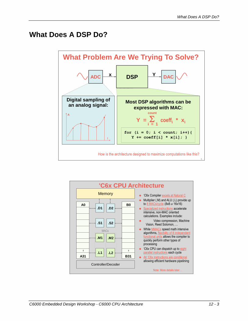
What Does A DSP Do?
What Problem Are We Trying To Solve?
Digital sampling of an analog signal:
A
t
Most DSP algorithms can be
expressed with MAC:
i = 1Y = coeffi * xi
count
for (i = 0; i < count; i++){
Y += coeff[i] * x[i]; }
DACx Y
ADC DSP
How is the architecture designed to maximize computations like this?5
'C6x CPU Architecture
Memory ‘C6x Compiler excels at Natural C
Multiplier (.M) and ALU (.L) provide up to 8 MACs/cycle (8x8 or 16x16)
Specialized instructions accelerate intensive, non-MAC oriented calculations. Examples include:
Video compression, Machine Vision, Reed Solomon, …
While MMACs speed math intensive algorithms, flexibility of 8 independent functional units allows the compiler to quickly perform other types of processing
‘C6x CPU can dispatch up to eight parallel instructions each cycle
All ‘C6x instructions are conditionalallowing efficient hardware pipelining
A0
A31
..
.S1
.D1
.L1
.S2
.M1 .M2
.D2
.L2
B0
B31
..
Controller/Decoder
MACs
Note: More details later…
CPU – From the Inside – Out…
12 - 4 C6000 Embedded Design Workshop - C6000 CPU Architecture
CPU – From the Inside – Out…
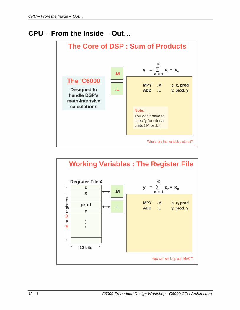
Mult
ALUMPY c, x, prod
ADD y, prod, y
y =
40
cn xnn = 1
*
The Core of DSP : Sum of Products
The ‘C6000
Designed to
handle DSP’s
math-intensive
calculations
ALU
.M
MPY .M c, x, prod.L ADD .L y, prod, y
Note:
You don’t have to
specify functional
units (.M or .L)
Where are the variables stored?8
y =
40
cn xnn = 1
*
Register File A
c
x
prod
32-bits
y
.
.
.
.M
.L
Working Variables : The Register File
16
or
32
reg
iste
rs
MPY .M c, x, prod
ADD .L y, prod, y
How can we loop our ‘MAC’?9
CPU – From the Inside – Out…
C6000 Embedded Design Workshop - C6000 CPU Architecture 12 - 5
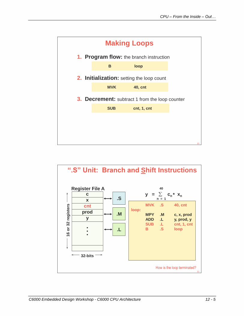
Making Loops
1. Program flow: the branch instruction
2. Initialization: setting the loop count
3. Decrement: subtract 1 from the loop counter
B loop
SUB cnt, 1, cnt
MVK 40, cnt
10
y =
40
cn xnn = 1
*
“.S” Unit: Branch and Shift Instructions
MVK .S 40, cnt
loop:
MPY .M c, x, prod
ADD .L y, prod, y
SUB .L cnt, 1, cnt
B .S loop
.M
.L
.S
Register File A
32-bits
c
x
prod
y
.
.
.
cnt
How is the loop terminated?
16 o
r 32 r
eg
iste
rs
11
CPU – From the Inside – Out…
12 - 6 C6000 Embedded Design Workshop - C6000 CPU Architecture
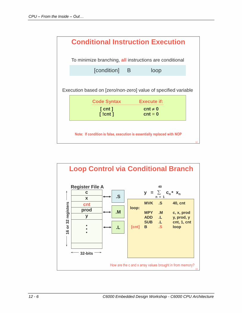
Conditional Instruction Execution
Note: If condition is false, execution is essentially replaced with NOP
Code Syntax Execute if:
[ cnt ] cnt 0[ !cnt ] cnt = 0
Execution based on [zero/non-zero] value of specified variable
To minimize branching, all instructions are conditional
[condition] B loop
12
y =
40
cn xnn = 1
*
Loop Control via Conditional Branch
MVK .S 40, cnt
loop:
MPY .M c, x, prod
ADD .L y, prod, y
SUB .L cnt, 1, cnt
[cnt] B .S loop
.M
.L
.S
Register File A
32-bits
c
x
prod
y
.
.
.
cnt
How are the c and x array values brought in from memory?
16 o
r 32 r
eg
iste
rs
13
CPU – From the Inside – Out…
C6000 Embedded Design Workshop - C6000 CPU Architecture 12 - 7
Memory Access via “.D” Unit
.M
.L
.S y =
40
cn xnn = 1
*
MVK .S 40, cnt
loop:
LDH .D *cp , c
LDH .D *xp , x
MPY .M c, x, prod
ADD .L y, prod, y
SUB .L cnt, 1, cnt
[cnt] B .S loop
Data Memory:x(40), a(40), y
Register File Ac
x
prod
y
cnt
*cp
*xp
*yp
.D
What does the “H” in LDH signify?
16 o
r 32 r
eg
iste
rs
Note: No restrictions on which regs can be
used for address or data!
14
Memory Access via “.D” Unit
.M
.L
.S y =
40
cn xnn = 1
*
MVK .S 40, cnt
loop:
LDH .D *cp , c
LDH .D *xp , x
MPY .M c, x, prod
ADD .L y, prod, y
SUB .L cnt, 1, cnt
[cnt] B .S loop
Data Memory:x(40), a(40), y
Register File A
c
x
prod
y
cnt
*cp
*xp
*yp
.D
How do we increment through the arrays?
16 o
r 32 r
eg
iste
rs
Instr. Description C Type Size
LDB load byte char 8-bits
LDH load half-word short 16-bits
LDW load word int 32-bits
LDDW* load double-word double 64-bits
* Except C62x & C67x generations
15
CPU – From the Inside – Out…
12 - 8 C6000 Embedded Design Workshop - C6000 CPU Architecture
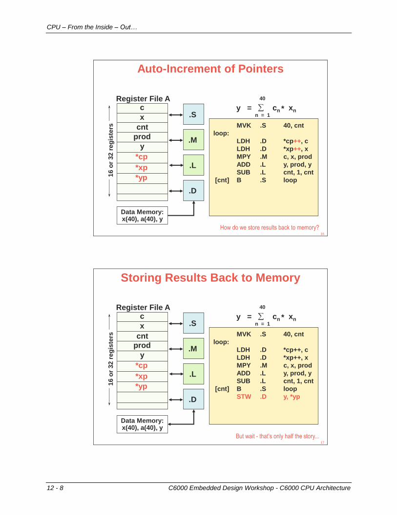
Auto-Increment of Pointers
Register File Ac
x
prod
y
cnt
*cp
*xp
*yp
y =
40
cn xnn = 1
*
MVK .S 40, cnt
loop:
LDH .D *cp++, c
LDH .D *xp++, x
MPY .M c, x, prod
ADD .L y, prod, y
SUB .L cnt, 1, cnt
[cnt] B .S loop
.M
.L
.S
Data Memory:x(40), a(40), y
.D
How do we store results back to memory?
16 o
r 32 r
eg
iste
rs
16
Storing Results Back to Memory
Register File Ac
x
prod
y
cnt
*cp
*xp
*yp
y =
40
cn xnn = 1
*
MVK .S 40, cnt
loop:
LDH .D *cp++, c
LDH .D *xp++, x
MPY .M c, x, prod
ADD .L y, prod, y
SUB .L cnt, 1, cnt
[cnt] B .S loop
STW .D y, *yp
.M
.L
.S
Data Memory:x(40), a(40), y
.D
But wait - that’s only half the story...
16 o
r 32 r
eg
iste
rs
17
CPU – From the Inside – Out…
C6000 Embedded Design Workshop - C6000 CPU Architecture 12 - 9
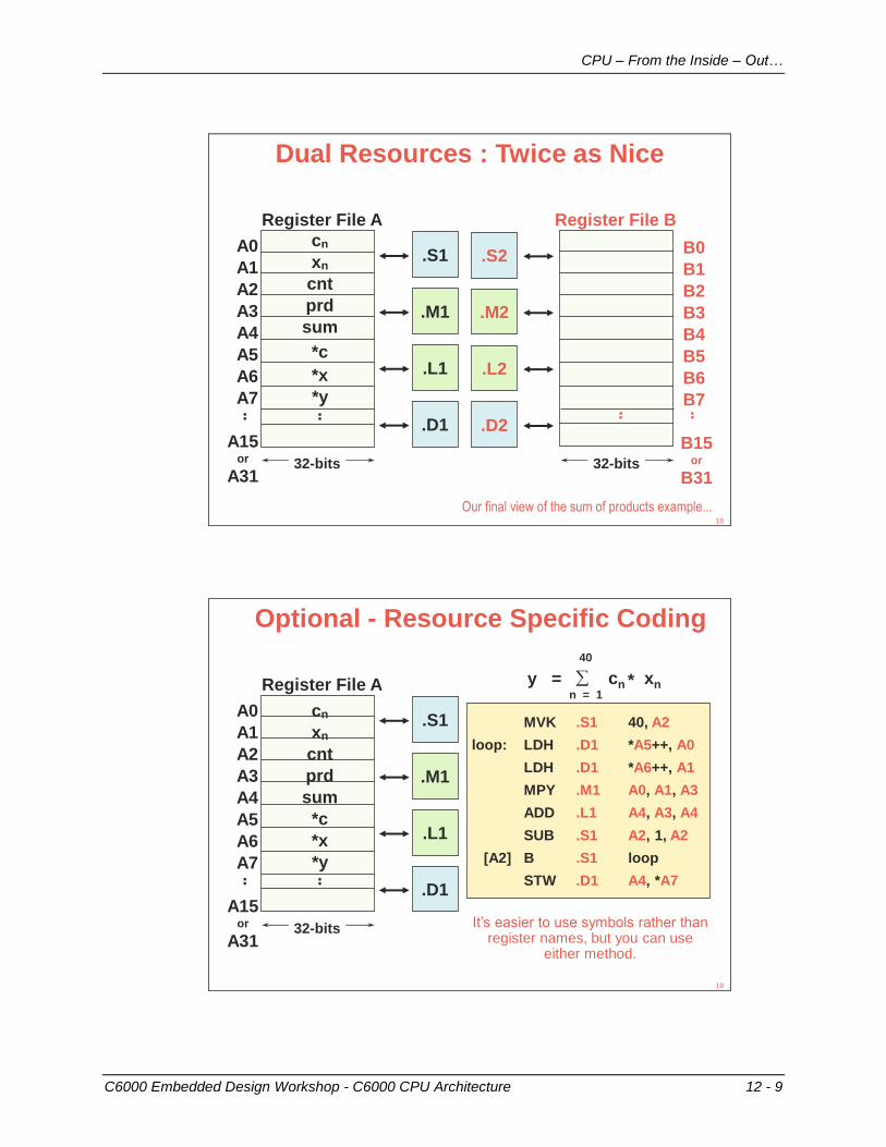
Dual Resources : Twice as Nice
A0
A1
A2
A3
A4
Register File A
A15or
A31
A5
A6
A7
cn
xn
prd
sum
cnt
..
*c
*x
*y
.M1
.L1
.S1
.D1
.M2
.L2
.S2
.D2
Register File B
B0
B1
B2
B3
B4
B15or
B31
B5
B6
B7..
32-bits
....
32-bits
Our final view of the sum of products example...18
MVK .S1 40, A2
loop: LDH .D1 *A5++, A0
LDH .D1 *A6++, A1
MPY .M1 A0, A1, A3
ADD .L1 A4, A3, A4
SUB .S1 A2, 1, A2
[A2] B .S1 loop
STW .D1 A4, *A7
y =
40
cn xnn = 1
*
Optional - Resource Specific Coding
A0
A1
A2
A3
A4
Register File A
A15or
A31
A5
A6
A7
cn
xn
prd
sum
cnt
..
*c
*x
*y
.M1
.L1
.S1
.D1
32-bits
..
It’s easier to use symbols rather thanregister names, but you can use
either method.
19
Instruction Sets
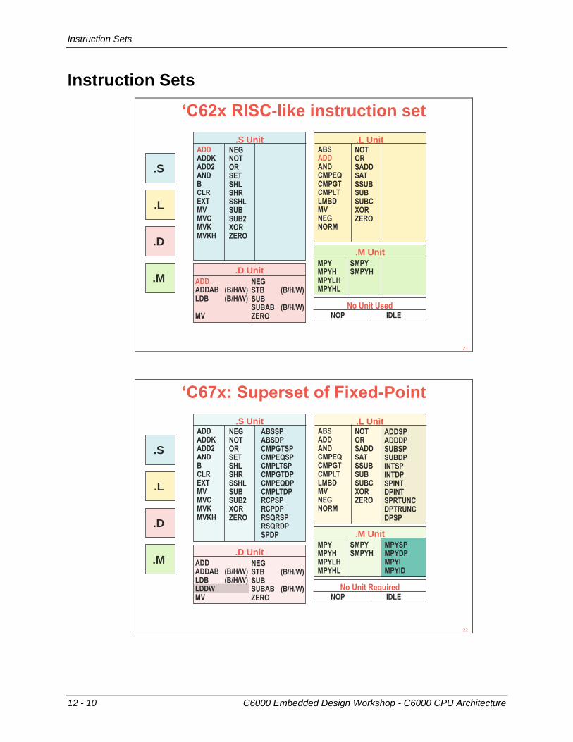
12 - 10 C6000 Embedded Design Workshop - C6000 CPU Architecture
Instruction Sets
‘C62x RISC-like instruction set
.L
.D
.S
.M
No Unit UsedIDLENOP
.S UnitNEGNOT ORSETSHLSHRSSHLSUBSUB2XORZERO
ADDADDKADD2ANDBCLREXTMVMVCMVKMVKH
.L UnitNOTORSADDSATSSUBSUBSUBCXORZERO
ABSADDANDCMPEQCMPGTCMPLTLMBDMVNEGNORM
.M Unit
SMPYSMPYH
MPYMPYHMPYLHMPYHL
.D Unit
NEGSTB (B/H/W) SUBSUBAB (B/H/W) ZERO
ADDADDAB (B/H/W)LDB (B/H/W)
MV
21
‘C67x: Superset of Fixed-Point
.L
.D
.S
.M
No Unit RequiredIDLENOP
.S UnitNEGNOT ORSETSHLSHRSSHLSUBSUB2XORZERO
ADDADDKADD2ANDBCLREXTMVMVCMVKMVKH
ABSSPABSDPCMPGTSPCMPEQSPCMPLTSPCMPGTDPCMPEQDPCMPLTDPRCPSPRCPDPRSQRSPRSQRDPSPDP
.L UnitNOTORSADDSATSSUBSUBSUBCXORZERO
ABSADDANDCMPEQCMPGTCMPLTLMBDMVNEGNORM
ADDSPADDDPSUBSPSUBDPINTSPINTDPSPINTDPINTSPRTUNCDPTRUNCDPSP
.M Unit
SMPYSMPYH
MPYMPYHMPYLHMPYHL
MPYSPMPYDPMPYIMPYID
.D Unit
NEGSTB (B/H/W) SUBSUBAB (B/H/W) ZERO
ADDADDAB (B/H/W)LDB (B/H/W)LDDWMV
22
Instruction Sets
C6000 Embedded Design Workshop - C6000 CPU Architecture 12 - 11
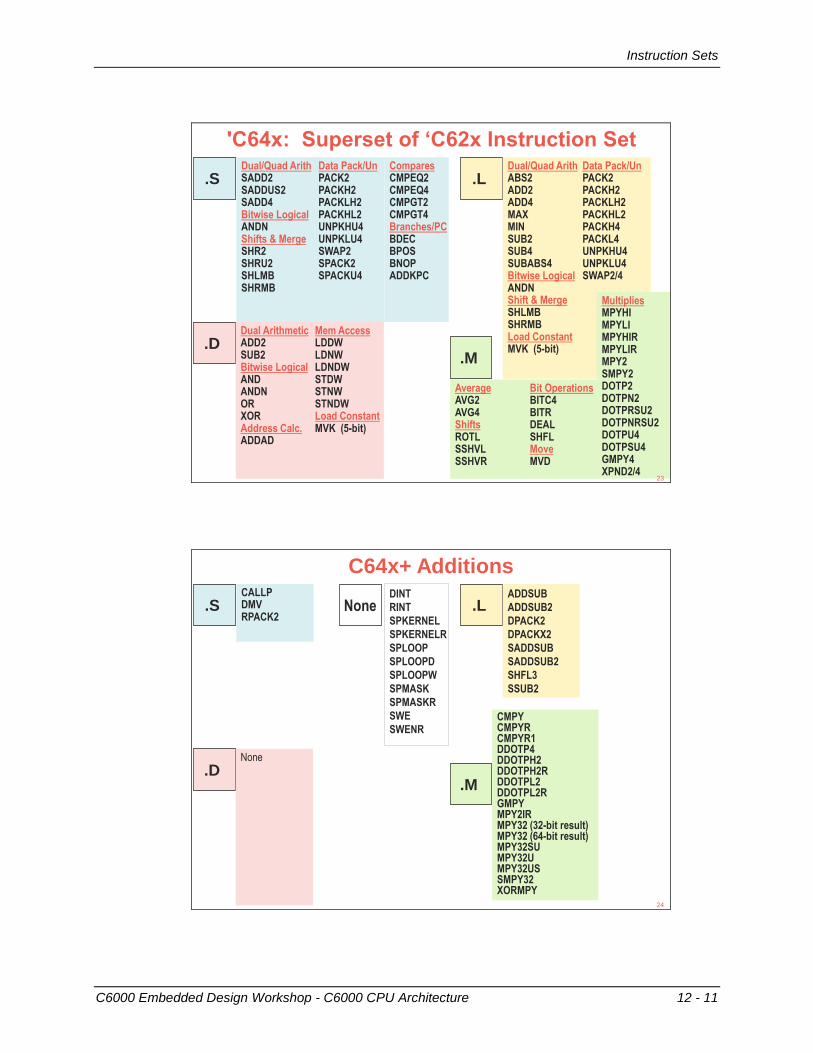
'C64x: Superset of ‘C62x Instruction Set
.L Data Pack/UnPACK2PACKH2PACKLH2PACKHL2PACKH4PACKL4UNPKHU4UNPKLU4SWAP2/4
Dual/Quad ArithABS2ADD2ADD4MAXMINSUB2SUB4SUBABS4Bitwise LogicalANDNShift & MergeSHLMBSHRMBLoad ConstantMVK (5-bit).D
.S
.M
Bit OperationsBITC4BITRDEALSHFLMoveMVD
AverageAVG2AVG4ShiftsROTLSSHVLSSHVR
MultipliesMPYHIMPYLIMPYHIRMPYLIRMPY2SMPY2DOTP2DOTPN2DOTPRSU2DOTPNRSU2DOTPU4DOTPSU4GMPY4XPND2/4
Mem AccessLDDWLDNWLDNDWSTDWSTNWSTNDWLoad ConstantMVK (5-bit)
Dual ArithmeticADD2SUB2Bitwise LogicalANDANDNORXORAddress Calc.ADDAD
Data Pack/UnPACK2PACKH2PACKLH2PACKHL2UNPKHU4UNPKLU4SWAP2SPACK2SPACKU4
Dual/Quad ArithSADD2SADDUS2SADD4Bitwise LogicalANDNShifts & MergeSHR2SHRU2SHLMBSHRMB
ComparesCMPEQ2CMPEQ4CMPGT2CMPGT4Branches/PCBDECBPOSBNOPADDKPC
23
C64x+ Additions
.L ADDSUB
ADDSUB2
DPACK2
DPACKX2
SADDSUB
SADDSUB2
SHFL3
SSUB2
.D
.S
.M
CMPYCMPYRCMPYR1DDOTP4DDOTPH2DDOTPH2RDDOTPL2DDOTPL2RGMPYMPY2IRMPY32 (32-bit result)MPY32 (64-bit result)MPY32SUMPY32UMPY32USSMPY32XORMPY
None
CALLPDMVRPACK2
None
24
DINT
RINT
SPKERNEL
SPKERNELR
SPLOOP
SPLOOPD
SPLOOPW
SPMASK
SPMASKR
SWE
SWENR
“MAC” Instructions
12 - 12 C6000 Embedded Design Workshop - C6000 CPU Architecture
“MAC” Instructions
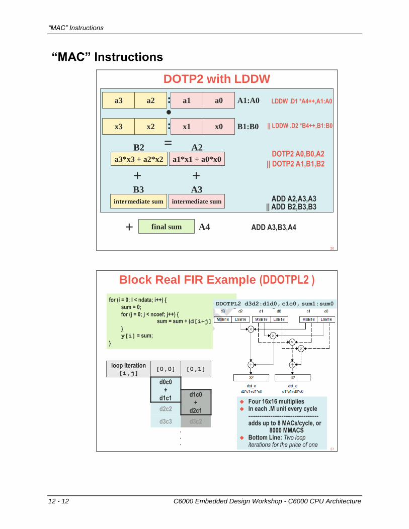
DOTP2 with LDDW
=
+
a2 a0 A1:A0 LDDW .D1 *A4++,A1:A0
|| LDDW .D2 *B4++,B1:B0
A2B2
a3*x3 + a2*x2 a1*x1 + a0*x0DOTP2 A0,B0,A2
|| DOTP2 A1,B1,B2
+
intermediate sum ADD A2,A3,A3
a1a3 :
A5
x2 x0 B1:B0x1x3 :
final sum ADD A3,B3,A4A4+
|| ADD B2,B3,B3intermediate sum
A3B3
26
Block Real FIR Example (DDOTPL2 )
for (i = 0; I < ndata; i++) {
sum = 0;
for (j = 0; j < ncoef; j++) {sum = sum + (d[i+j] * c[j]);
}y[i] = sum;
}
loop Iteration[i,j]
[0,0] [0,1]
d0c0
+
d1c1d1c0
+
d2c1d2c2
d3c3 d3c2
.
.
.
Four 16x16 multiplies In each .M unit every cycle
--------------------------------------adds up to 8 MACs/cycle, or
8000 MMACS Bottom Line: Two loop
iterations for the price of one
DDOTPL2 d3d2:d1d0, c1c0, sum1:sum0
27
“MAC” Instructions
C6000 Embedded Design Workshop - C6000 CPU Architecture 12 - 13
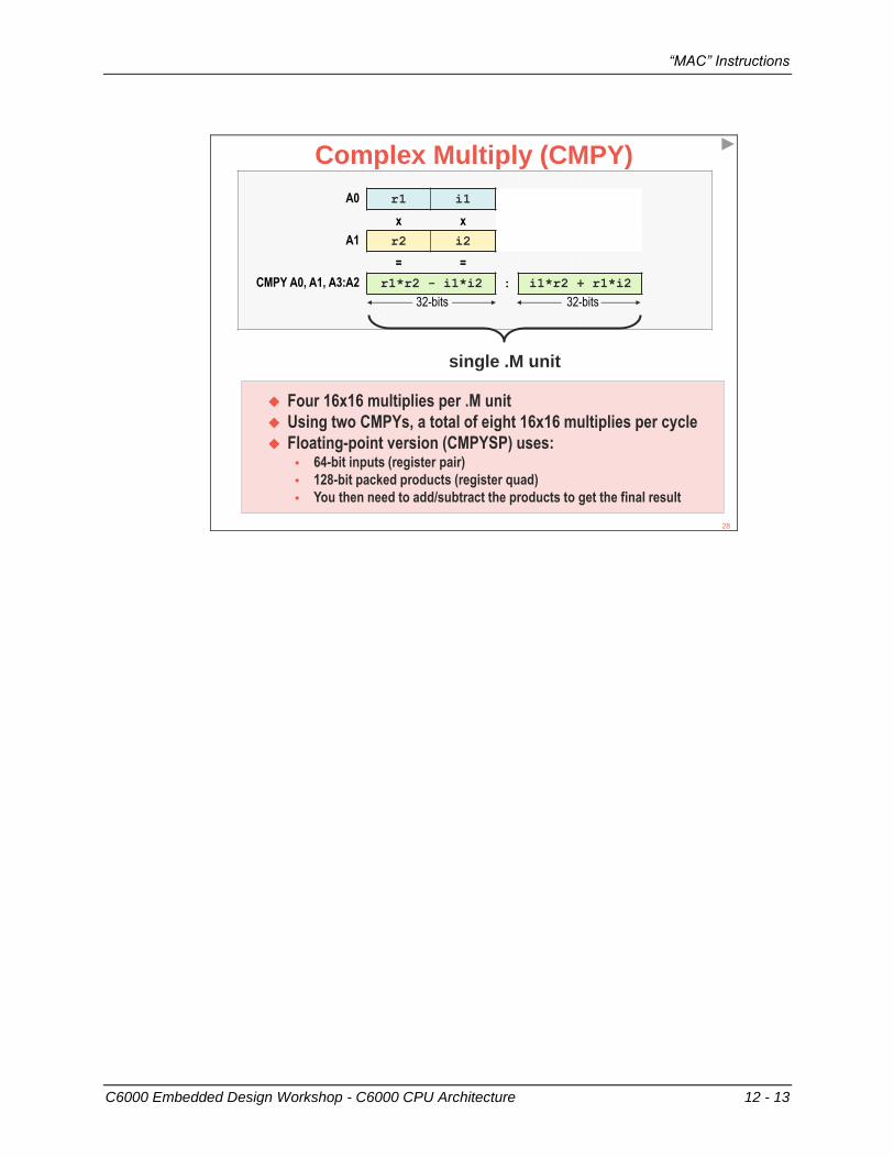
Complex Multiply (CMPY)
A0 r1 i1
x x
A1 r2 i2
= =
CMPY A0, A1, A3:A2 r1*r2 - i1*i2 : i1*r2 + r1*i2
32-bits 32-bits
Four 16x16 multiplies per .M unit
Using two CMPYs, a total of eight 16x16 multiplies per cycle
Floating-point version (CMPYSP) uses: 64-bit inputs (register pair)
128-bit packed products (register quad)
You then need to add/subtract the products to get the final result
single .M unit
28
C66x – “MAC” Instructions
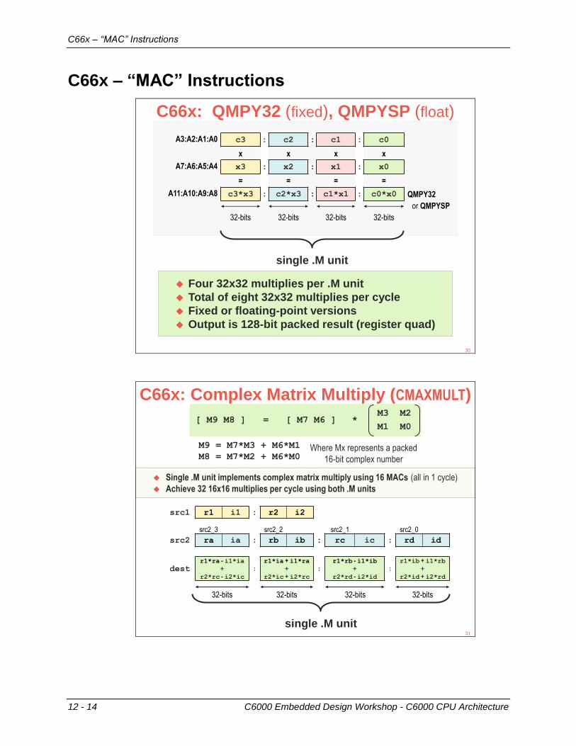
12 - 14 C6000 Embedded Design Workshop - C6000 CPU Architecture
C66x – “MAC” Instructions
C66x: QMPY32 (fixed), QMPYSP (float)
A3:A2:A1:A0 c3 : c2 : c1 : c0
x x x x
A7:A6:A5:A4 x3 : x2 : x1 : x0
= = = =
A11:A10:A9:A8 c3*x3 : c2*x3 : c1*x1 : c0*x0 QMPY32
or QMPYSP
32-bits 32-bits 32-bits 32-bits
Four 32x32 multiplies per .M unit
Total of eight 32x32 multiplies per cycle
Fixed or floating-point versions
Output is 128-bit packed result (register quad)
single .M unit
30
C66x: Complex Matrix Multiply (CMAXMULT)
src1 r1 i1 : r2 i2
src2_3 src2_2 src2_1 src2_0
src2 ra ia : rb ib : rc ic : rd id
destr1*ra - i1*ia
+
r2*rc - i2*ic
:
r1*ia + i1*ra+
r2*ic + i2*rc
:
r1*rb - i1*ib+
r2*rd - i2*id
:
r1*ib + i1*rb+
r2*id + i2*rd
single .M unit
32-bits 32-bits 32-bits 32-bits
Single .M unit implements complex matrix multiply using 16 MACs (all in 1 cycle)
Achieve 32 16x16 multiplies per cycle using both .M units
[ M9 M8 ] = [ M7 M6 ] *M3 M2
M1 M0
M9 = M7*M3 + M6*M1
M8 = M7*M2 + M6*M0Where Mx represents a packed
16-bit complex number
31
Hardware Pipeline
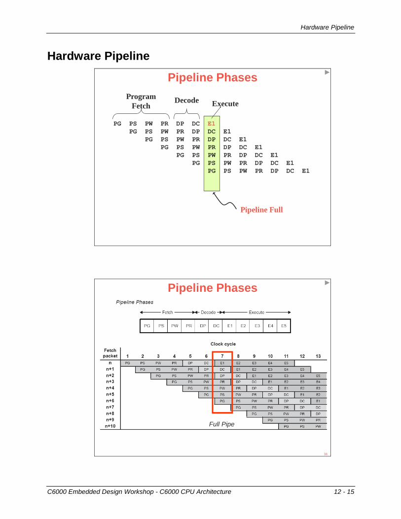
C6000 Embedded Design Workshop - C6000 CPU Architecture 12 - 15
Hardware Pipeline
Pipeline Full
PG PS PW PR DP DC E1
PG PS PW PR DP DC E1
PG PS PW PR DP DC E1
PG PS PW PR DP DC E1
PG PS PW PR DP DC E1
PG PS PW PR DP DC E1
PG PS PW PR DP DC E1
Program
Fetch ExecuteDecode
Pipeline Phases
Pipeline Phases
Full Pipe
34
Software Pipelining
12 - 16 C6000 Embedded Design Workshop - C6000 CPU Architecture
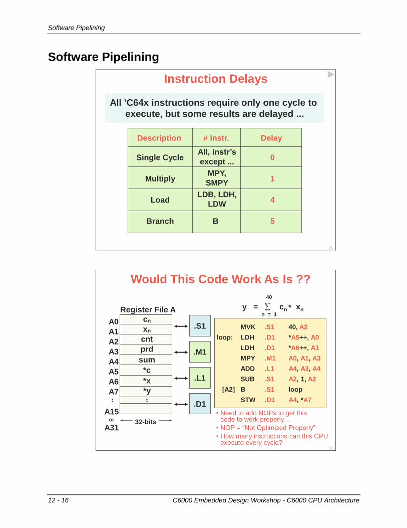
Software Pipelining
Single Cycle 0
Multiply 1
Load 4
Branch B 5
All, instr’s
except ...
MPY,
SMPY
LDB, LDH,
LDW
Description # Instr. Delay
All 'C64x instructions require only one cycle to
execute, but some results are delayed ...
Instruction Delays
36
MVK .S1 40, A2
loop: LDH .D1 *A5++, A0
LDH .D1 *A6++, A1
MPY .M1 A0, A1, A3
ADD .L1 A4, A3, A4
SUB .S1 A2, 1, A2
[A2] B .S1 loop
STW .D1 A4, *A7
y =
40
cn xnn = 1
*
Would This Code Work As Is ??
A0
A1
A2
A3
A4
Register File A
A15or
A31
A5
A6
A7
cn
xn
prd
sum
cnt
..
*c
*x
*y
.M1
.L1
.S1
.D1
32-bits
..
• Need to add NOPs to get thiscode to work properly…
• NOP = “Not Optimized Properly”
• How many instructions can this CPUexecute every cycle?
37

Software Pipelining
C6000 Embedded Design Workshop - C6000 CPU Architecture 12 - 17
Software Pipelined Algorithm
.L1
.L2
.S1
.S2
.M1
.M2
.D1
.D2
add
mpy3mpy2mpy
76543210
ldw8ldw7ldw6ldw5ldw4ldw3ldw2ldw m
ldw8ldw7ldw6ldw5ldw4ldw3ldw2ldw n
1
4
mpyh3mpyh2mpyh
sub7sub6sub5sub4sub3sub2sub
add
B6B5B4B3B2B
2
7
5
8
LOOPPROLOG
3
6
38
Software Pipelined ‘C6x Code
c0: ldw .D1 *A4++,A5
|| ldw .D2 *B4++,B5
c1: ldw .D1 *A4++,A5
|| ldw .D2 *B4++,B5
|| [B0] sub .S2 B0,1,B0
c2_3_4: ldw .D1 *A4++,A5
|| ldw .D2 *B4++,B5
|| [B0] sub .S2 B0,1,B0
|| [B0] B .S1 loop
.
.
.
c5_6: ldw .D1 *A4++,A5
|| ldw .D2 *B4++,B5
|| [B0] sub .S2 B0,1,B0
|| [B0] B .S1 loop
|| mpy .M1x A5,B5,A6
|| mpyh .M2x A5,B5,B6
.
.*** Single-Cycle Loop
loop: ldw .D1 *A4++,A5
|| ldw .D2 *B4++,B5
|| [B0] sub .S2 B0,1,B0
|| [B0] B .S1 loop
|| mpy .M1x A5,B5,A6
|| mpyh.M2x A5,B5,B6
|| add .L1 A7,A6,A7
|| add .L2 B7,B6,B7
39
Software Pipelining
12 - 18 C6000 Embedded Design Workshop - C6000 CPU Architecture
*** this page contains no useful information ***
Chapter Quiz
C6000 Embedded Design Workshop - C6000 CPU Architecture 12 - 19
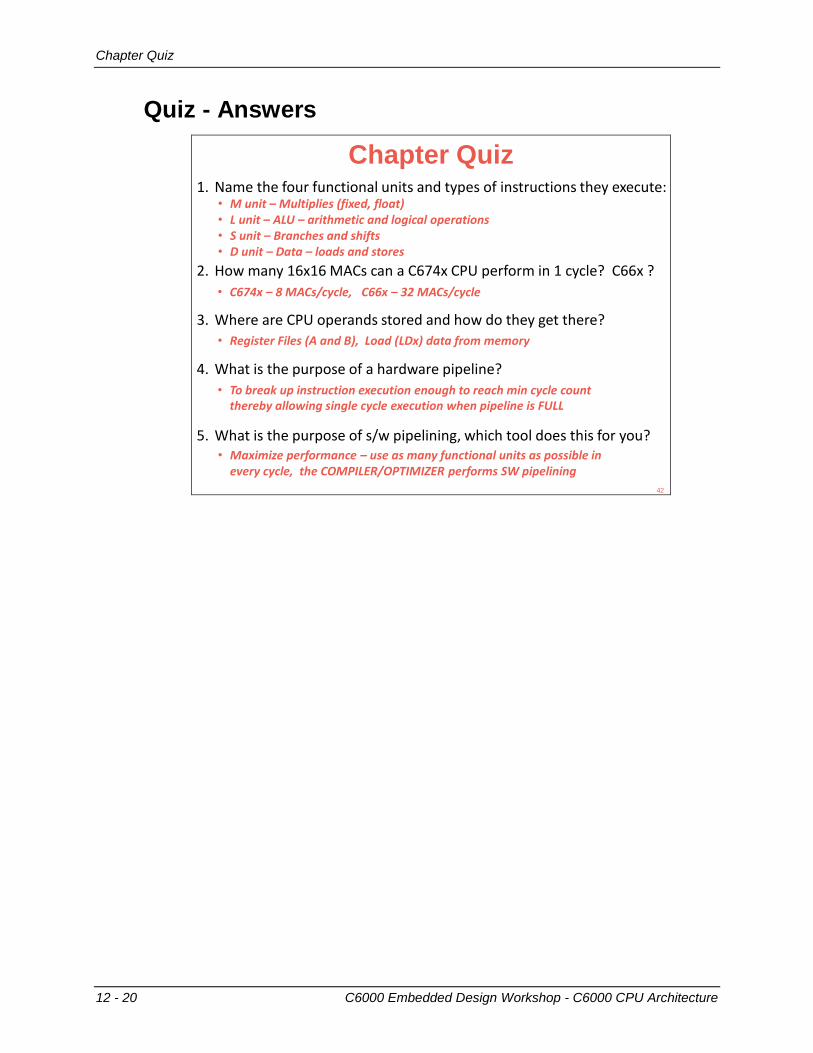
Chapter Quiz
Chapter Quiz1. Name the four functional units and types of instructions they execute:
2. How many 16x16 MACs can a C674x CPU perform in 1 cycle? C66x ?
3. Where are CPU operands stored and how do they get there?
4. What is the purpose of a hardware pipeline?
5. What is the purpose of s/w pipelining, which tool does this for you?
Chapter Quiz
12 - 20 C6000 Embedded Design Workshop - C6000 CPU Architecture
Quiz - Answers
Chapter Quiz1. Name the four functional units and types of instructions they execute:
2. How many 16x16 MACs can a C674x CPU perform in 1 cycle? C66x ?
3. Where are CPU operands stored and how do they get there?
4. What is the purpose of a hardware pipeline?
5. What is the purpose of s/w pipelining, which tool does this for you?
• M unit – Multiplies (fixed, float)• L unit – ALU – arithmetic and logical operations• S unit – Branches and shifts• D unit – Data – loads and stores
• C674x – 8 MACs/cycle, C66x – 32 MACs/cycle
• Register Files (A and B), Load (LDx) data from memory
• Maximize performance – use as many functional units as possible inevery cycle, the COMPILER/OPTIMIZER performs SW pipelining
• To break up instruction execution enough to reach min cycle countthereby allowing single cycle execution when pipeline is FULL
42
C6000 Embedded Design Workshop - C and System Optimizations 13 - 1
C and System Optimizations
Introduction
In this chapter, we will cover the basics of optimizing C code and some useful tips on system optimization. Also included here are some other system-wide optimizations you can take advantage of in your own application.
Outline
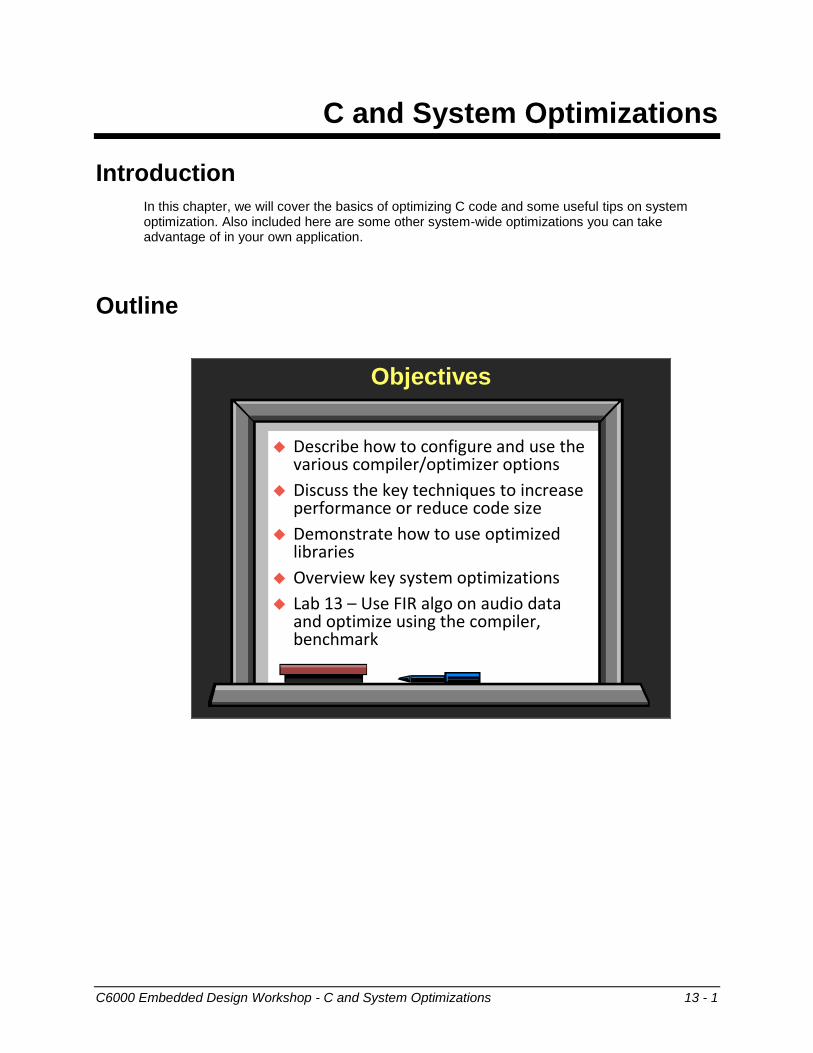
Objectives
Describe how to configure and use the various compiler/optimizer options
Discuss the key techniques to increaseperformance or reduce code size
Demonstrate how to use optimized libraries
Overview key system optimizations
Lab 13 – Use FIR algo on audio data and optimize using the compiler, benchmark
Module Topics
13 - 2 C6000 Embedded Design Workshop - C and System Optimizations
Module Topics
C and System Optimizations ................................................................................................... 13-1
Module Topics ......................................................................................................................... 13-2
Introduction – “Optimal” and “Optimization” ............................................................................ 13-3
C Compiler and Optimizer ....................................................................................................... 13-5 “Debug” vs. “Optimized” ...................................................................................................... 13-5 Levels of Optimization ......................................................................................................... 13-6 Build Configurations ............................................................................................................ 13-7 Code Space Optimization (–ms) ......................................................................................... 13-8 File and Function Specific Options ..................................................................................... 13-9 Coding Guidelines ............................................................................................................. 13-10
Data Types and Alignment .................................................................................................... 13-11 Data Types ........................................................................................................................ 13-11 Data Alignment .................................................................................................................. 13-12 Forcing Data Alignment ..................................................................................................... 13-13
Restricting Memory Dependencies (Aliasing) ....................................................................... 13-14
Access Hardware Features – Using Intrinsics ...................................................................... 13-16
Give Compiler MORE Information ........................................................................................ 13-17 Pragma – Unroll() .............................................................................................................. 13-17 Pragma – MUST_ITERATE() ............................................................................................ 13-18 Keyword - Volatile ............................................................................................................. 13-18 Setting MAX interrupt Latency (-mi option) ....................................................................... 13-19 Compiler Directive - _nassert() ......................................................................................... 13-20
Using Optimized Libraries ..................................................................................................... 13-21 Libraries – Download and Support .................................................................................... 13-23
System Optimizations ........................................................................................................... 13-24 Custom Sections ............................................................................................................... 13-24 Use EDMA......................................................................................................................... 13-25 Use Cache......................................................................................................................... 13-26 System Architecture – SCR .............................................................................................. 13-26
Chapter Quiz ......................................................................................................................... 13-27 Quiz - Answers .................................................................................................................. 13-28
Lab 13 – C Optimizations ...................................................................................................... 13-29
Lab 13 – C Optimizations – Procedure ................................................................................. 13-30 PART A – Goals and Using Compiler Options.................................................................. 13-30
Determine Goals and CPU Min ..................................................................................... 13-30 Using Release Configuration (–o2, –g) ......................................................................... 13-33 Using “Opt” Configuration ............................................................................................. 13-36
Part B – Code Tuning ........................................................................................................ 13-39 Part C – Minimizing Code Size (–ms) ............................................................................... 13-40 Part D – Using DSPLib ...................................................................................................... 13-41 Conclusion......................................................................................................................... 13-42
Introduction – “Optimal” and “Optimization”
C6000 Embedded Design Workshop - C and System Optimizations 13 - 3
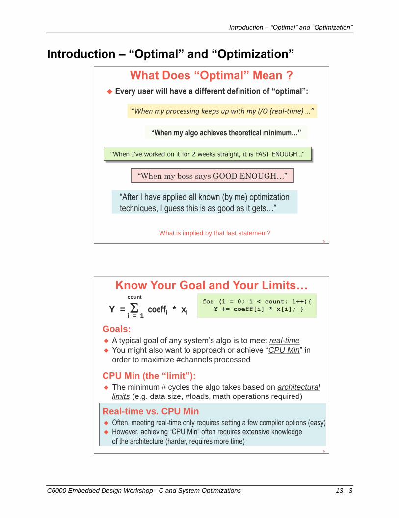
Introduction – “Optimal” and “Optimization”
What Does “Optimal” Mean ?
Every user will have a different definition of “optimal”:
“When my processing keeps up with my I/O (real-time) …”
“When my algo achieves theoretical minimum…”
“When I’ve worked on it for 2 weeks straight, it is FAST ENOUGH…”
“When my boss says GOOD ENOUGH…”
“After I have applied all known (by me) optimization
techniques, I guess this is as good as it gets…”
What is implied by that last statement?5
Know Your Goal and Your Limits…count
i = 1Y = coeffi * xi
for (i = 0; i < count; i++){
Y += coeff[i] * x[i]; }
A typical goal of any system’s algo is to meet real-time
You might also want to approach or achieve “CPU Min” in
order to maximize #channels processed
The minimum # cycles the algo takes based on architectural
limits (e.g. data size, #loads, math operations required)
Goals:
CPU Min (the “limit”):
Often, meeting real-time only requires setting a few compiler options (easy)
However, achieving “CPU Min” often requires extensive knowledge
of the architecture (harder, requires more time)
Real-time vs. CPU Min
6
Introduction – “Optimal” and “Optimization”
13 - 4 C6000 Embedded Design Workshop - C and System Optimizations
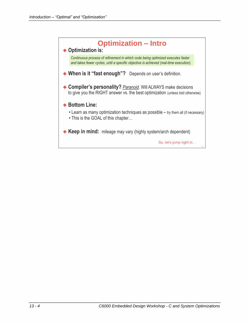
Optimization – Intro Optimization is:
So, let’s jump right in…
Continuous process of refinement in which code being optimized executes faster
and takes fewer cycles, until a specific objective is achieved (real-time execution).
When is it “fast enough”? Depends on user’s definition.
Bottom Line:
• Learn as many optimization techniques as possible – try them all (if necessary)
• This is the GOAL of this chapter…
Keep in mind: mileage may vary (highly system/arch dependent)
Compiler’s personality? Paranoid. Will ALWAYS make decisionsto give you the RIGHT answer vs. the best optimization (unless told otherwise)
7
C Compiler and Optimizer
C6000 Embedded Design Workshop - C and System Optimizations 13 - 5
C Compiler and Optimizer
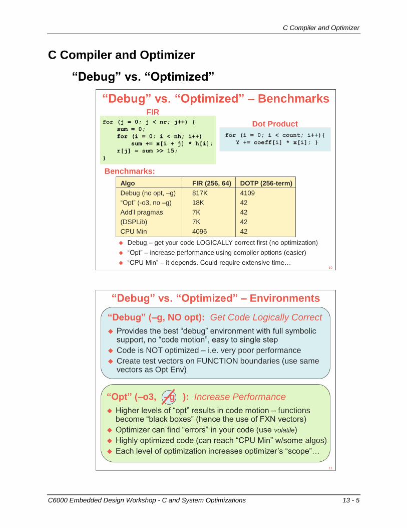
“Debug” vs. “Optimized”
“Debug” vs. “Optimized” – Benchmarks
for (j = 0; j < nr; j++) {
sum = 0;
for (i = 0; i < nh; i++)
sum += x[i + j] * h[i];
r[j] = sum >> 15;
}
for (i = 0; i < count; i++){
Y += coeff[i] * x[i]; }
FIR
Dot Product
Debug – get your code LOGICALLY correct first (no optimization)
“Opt” – increase performance using compiler options (easier)
“CPU Min” – it depends. Could require extensive time…
Benchmarks:
Algo FIR (256, 64) DOTP (256-term)
Debug (no opt, –g) 817K 4109
“Opt” (-o3, no –g) 18K 42
Add’l pragmas 7K 42
(DSPLib) 7K 42
CPU Min 4096 42
10
“Debug” vs. “Optimized” – Environments
Provides the best “debug” environment with full symbolicsupport, no “code motion”, easy to single step
Code is NOT optimized – i.e. very poor performance
Create test vectors on FUNCTION boundaries (use samevectors as Opt Env)
“Debug” (–g, NO opt): Get Code Logically Correct
Higher levels of “opt” results in code motion – functions become “black boxes” (hence the use of FXN vectors)
Optimizer can find “errors” in your code (use volatile)
Highly optimized code (can reach “CPU Min” w/some algos)
Each level of optimization increases optimizer’s “scope”…
“Opt” (–o3, –g ): Increase Performance
11
C Compiler and Optimizer
13 - 6 C6000 Embedded Design Workshop - C and System Optimizations
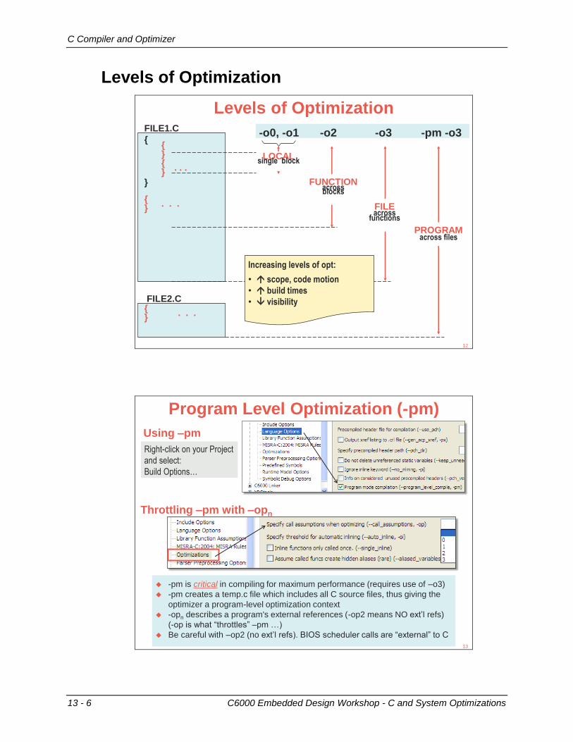
Levels of Optimization
Levels of OptimizationFILE1.C
{{}{
. . .}
}
{. . .
}
FILE2.C
-o0, -o1 -o2 -o3 -pm -o3
LOCALsingle block
FUNCTIONacrossblocks
FILEacross
functions
PROGRAMacross files
{. . .
}
Increasing levels of opt:
• scope, code motion
• build times
• visibility
12
Program Level Optimization (-pm)
-pm is critical in compiling for maximum performance (requires use of –o3)
-pm creates a temp.c file which includes all C source files, thus giving the
optimizer a program-level optimization context
-opn describes a program's external references (-op2 means NO ext’l refs)
(-op is what “throttles” –pm …)
Be careful with –op2 (no ext’l refs). BIOS scheduler calls are “external” to C
Right-click on your Project
and select:
Build Options…
Using –pm
Throttling –pm with –opn
13
C Compiler and Optimizer
C6000 Embedded Design Workshop - C and System Optimizations 13 - 7
Build Configurations
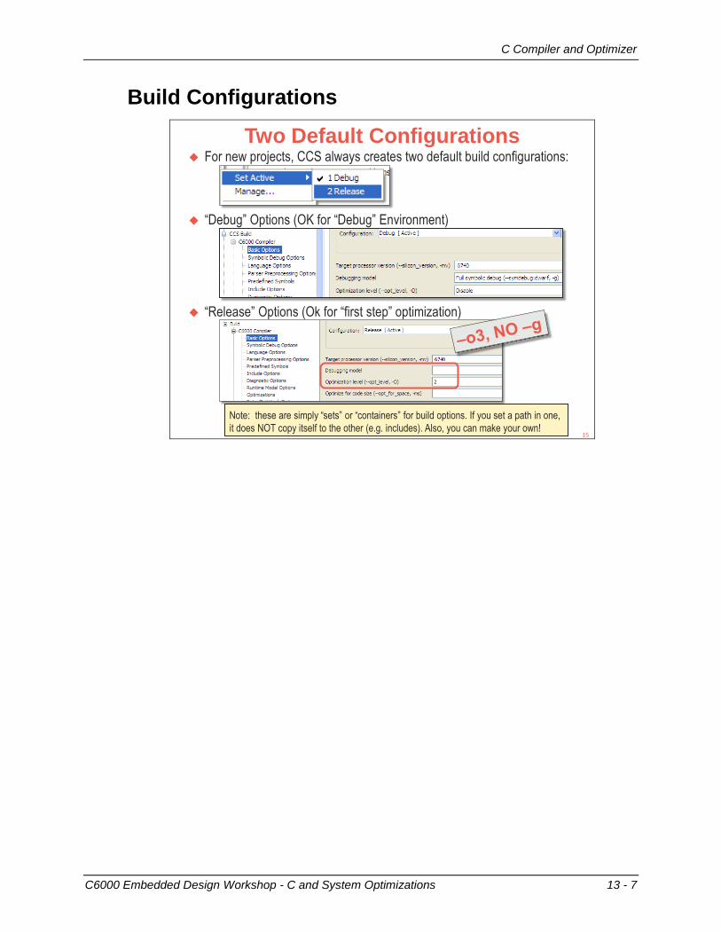
Two Default Configurations For new projects, CCS always creates two default build configurations:
“Debug” Options (OK for “Debug” Environment)
Note: these are simply “sets” or “containers” for build options. If you set a path in one,
it does NOT copy itself to the other (e.g. includes). Also, you can make your own!
“Release” Options (Ok for “first step” optimization)
15
C Compiler and Optimizer
13 - 8 C6000 Embedded Design Workshop - C and System Optimizations
Code Space Optimization (–ms)
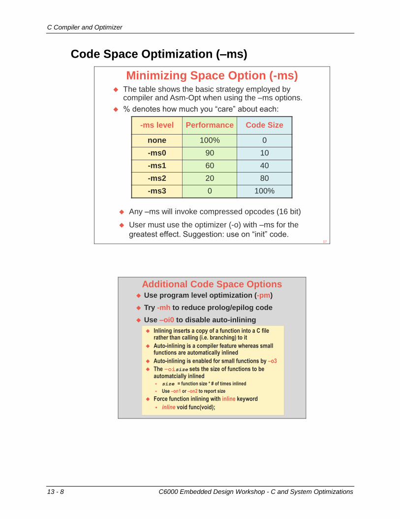
Minimizing Space Option (-ms) The table shows the basic strategy employed by
compiler and Asm-Opt when using the –ms options.
% denotes how much you “care” about each:
-ms level Performance Code Size
none 100% 0
-ms0 90 10
-ms1 60 40
-ms2 20 80
-ms3 0 100%
Any –ms will invoke compressed opcodes (16 bit)
User must use the optimizer (-o) with –ms for the
greatest effect. Suggestion: use on “init” code.17
Additional Code Space Options Use program level optimization (-pm)
Try -mh to reduce prolog/epilog code
Use –oi0 to disable auto-inlining
Inlining inserts a copy of a function into a C file rather than calling (i.e. branching) to it
Auto-inlining is a compiler feature whereas small functions are automatically inlined
Auto-inlining is enabled for small functions by –o3
The –oisize sets the size of functions to be automatcially inlined size = function size * # of times inlined
Use –on1 or –on2 to report size
Force function inlining with inline keyword
inline void func(void);
C Compiler and Optimizer
C6000 Embedded Design Workshop - C and System Optimizations 13 - 9
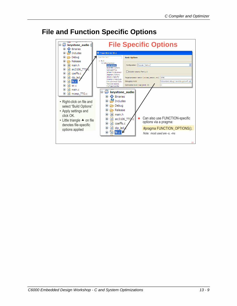
File and Function Specific Options
File Specific Options
• Right-click on file and
select “Build Options”
• Apply settings and
click OK.
• Little triangle on file
denotes file-specific
options applied
Can also use FUNCTION-specificoptions via a pragma:
#pragma FUNCTION_OPTIONS();
Note: most used are -o, -ms
20

C Compiler and Optimizer
13 - 10 C6000 Embedded Design Workshop - C and System Optimizations
Coding Guidelines
Programming the ‘C6000
Source Efficiency* Effort
80 - 100%C
C ++CompilerOptimizer
Low
95 - 100%Linear
ASMAssembly
OptimizerMed
100% HighASM Hand
Optimize
22
In order for the compiler to create the most efficient code, it is best to follow these guidelines:
Basic C Coding Guidelines
1. Use Minimum Complexity Code• If a human can’t understand and read it easily, neither can the compiler
• Break up larger “logic” into smaller loops/pieces
2. No function calls in tight loops• The compiler cannot create a pipelined loop with fxn calls present
3. Keep loops relatively small• Helps compiler generate tighter, more efficient pipelined loops
4. Create test vectors at FUNCTION boundaries• When optimization is turned on, it is nearly impossible to single-step inside fxns
5. Look at the assembly file – SPLOOP ?• If curious, look at the disassembly. Was SPLOOP/LDDW used or not? Why?
• Assembly optimizer generates comments as to what happened in the loop and why
• Use –mw (verbose pipeline info), -os (interlist), -k (keep .asm file) to see all info23
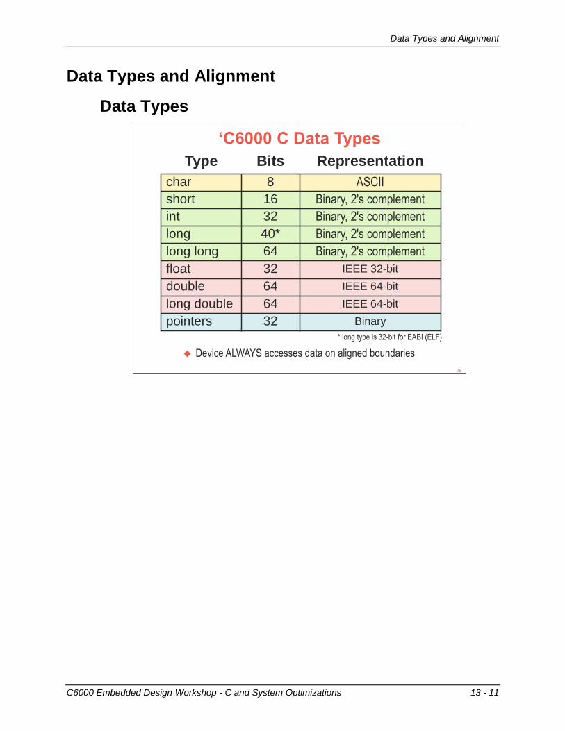
Data Types and Alignment
C6000 Embedded Design Workshop - C and System Optimizations 13 - 11
Data Types and Alignment
Data Types
‘C6000 C Data Types
Type Bits Representation
char 8 ASCII
short 16 Binary, 2's complement
int 32 Binary, 2's complement
long 40* Binary, 2's complement
long long 64 Binary, 2's complement
float 32 IEEE 32-bit
double 64 IEEE 64-bit
long double 64 IEEE 64-bit
pointers 32 Binary
* long type is 32-bit for EABI (ELF)
Device ALWAYS accesses data on aligned boundaries
26
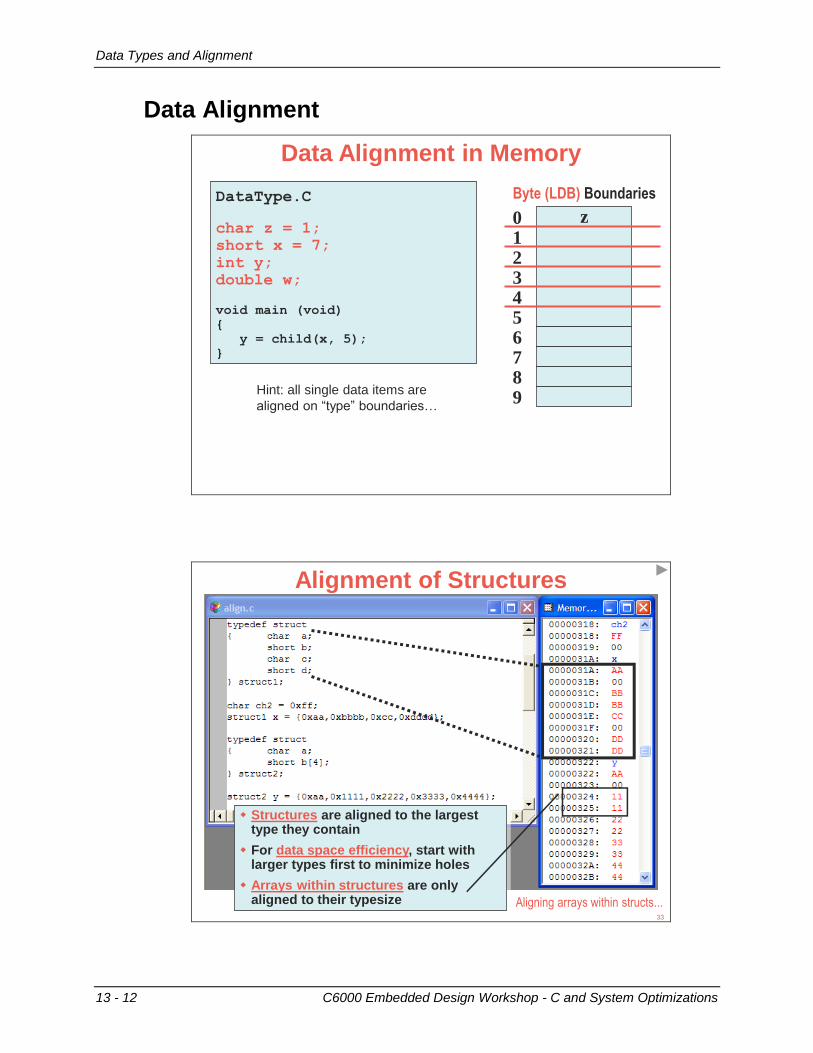
Data Types and Alignment
13 - 12 C6000 Embedded Design Workshop - C and System Optimizations
Data Alignment
Data Alignment in Memory
DataType.C
char z = 1;
short x = 7;
int y;
double w;
void main (void)
{
y = child(x, 5);
}
0123456789
z
Byte (LDB) Boundaries
Hint: all single data items are
aligned on “type” boundaries…
Alignment of Structures
Structures are aligned to the largest type they contain
For data space efficiency, start with larger types first to minimize holes
Arrays within structures are only aligned to their typesize Aligning arrays within structs...
33
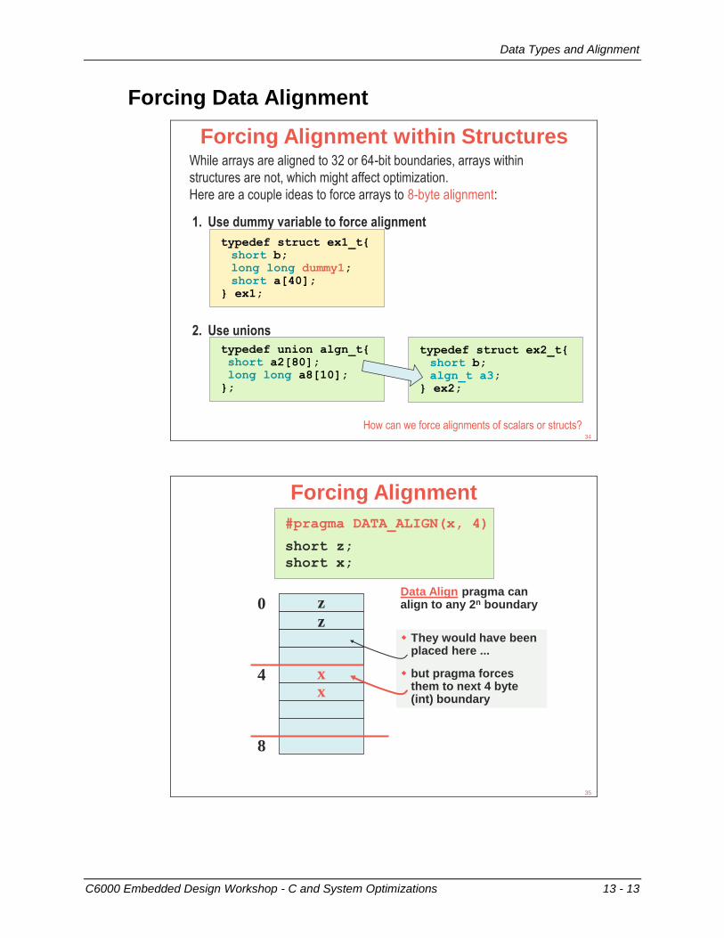
Data Types and Alignment
C6000 Embedded Design Workshop - C and System Optimizations 13 - 13
Forcing Data Alignment
Forcing Alignment within Structures
typedef struct ex1_t{
short b;
long long dummy1;
short a[40];
} ex1;
1. Use dummy variable to force alignment
2. Use unions
typedef union algn_t{
short a2[80];
long long a8[10];
};
While arrays are aligned to 32 or 64-bit boundaries, arrays within
structures are not, which might affect optimization.
Here are a couple ideas to force arrays to 8-byte alignment:
How can we force alignments of scalars or structs?
typedef struct ex2_t{
short b;
algn_t a3;
} ex2;
34
Forcing Alignment
#pragma DATA_ALIGN(x, 4)
short z;
short x;
0
4
8
z
zxxxx
Data Align pragma can align to any 2n boundary
They would have been placed here ...
but pragma forces them to next 4 byte (int) boundary
35
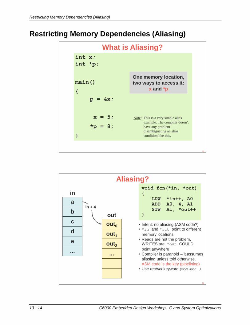
Restricting Memory Dependencies (Aliasing)
13 - 14 C6000 Embedded Design Workshop - C and System Optimizations
Restricting Memory Dependencies (Aliasing)
What is Aliasing?
int x;
int *p;
main()
{
p = &x;
x = 5;
*p = 8;
}
One memory location,
two ways to access it:
x and *p
Note: This is a very simple alias
example. The compiler doesn't
have any problem
disambiguating an alias
condition like this.
43
Aliasing?void fcn(*in, *out)
{
LDW *in++, A0
ADD A0, 4, A1
STW A1, *out++
}
out0
out1
out2
...
out
in + 4a
b
c
d
e
...
in
• Intent: no aliasing (ASM code?)• *in and *out point to different
memory locations
• Reads are not the problem,WRITES are. *out COULD
point anywhere
• Compiler is paranoid – it assumes
aliasing unless told otherwise.
ASM code is the key (pipelining)
• Use restrict keyword (more soon…)
44

Restricting Memory Dependencies (Aliasing)
C6000 Embedded Design Workshop - C and System Optimizations 13 - 15
Aliasing?
in + 4a
b
c
d
e
...
in
What happens if the function is called like this?
fcn(*myVector, *myVector+1)
void fcn(*in, *out)
{
LDW *in++, A0
ADD A0, 4, A1
STW A1, *out++
}
• Definitely Aliased pointers• *in and *out could point to
the same address
• But how does the compiler know?
• If you tell the compiler there is no
aliasing, this code will break (LDs
in software pipelined loop)
• One solution is to “restrict” thewrites - *out (see next slide…)
45
Alias Solutions1. Compiler solves most aliasing on its own.
If in doubt, the result will be correct even if the most optimal method won’t be used
2. Program Level Optimization (–pm –o3) Provide compiler visibility to entire program
3. No Bad Aliasing Option (–mt) Tell the compiler that no bad aliases exist in entire project See Compiler User's Guide for definition of “bad” Previous weighted vector summation example
performance was increased by 5x (by using –mt)
4. “Restrict” Keyword (ANSI C) Similar to –mt, but on a array-level basis
void fcn(short * in, short * restrict out)
Along with these suggestions, we highly recommend you check out:
TMS320C6000 Programmer’s Guide
TMS320C6000 Optimizing C Compiler User’s Guide46
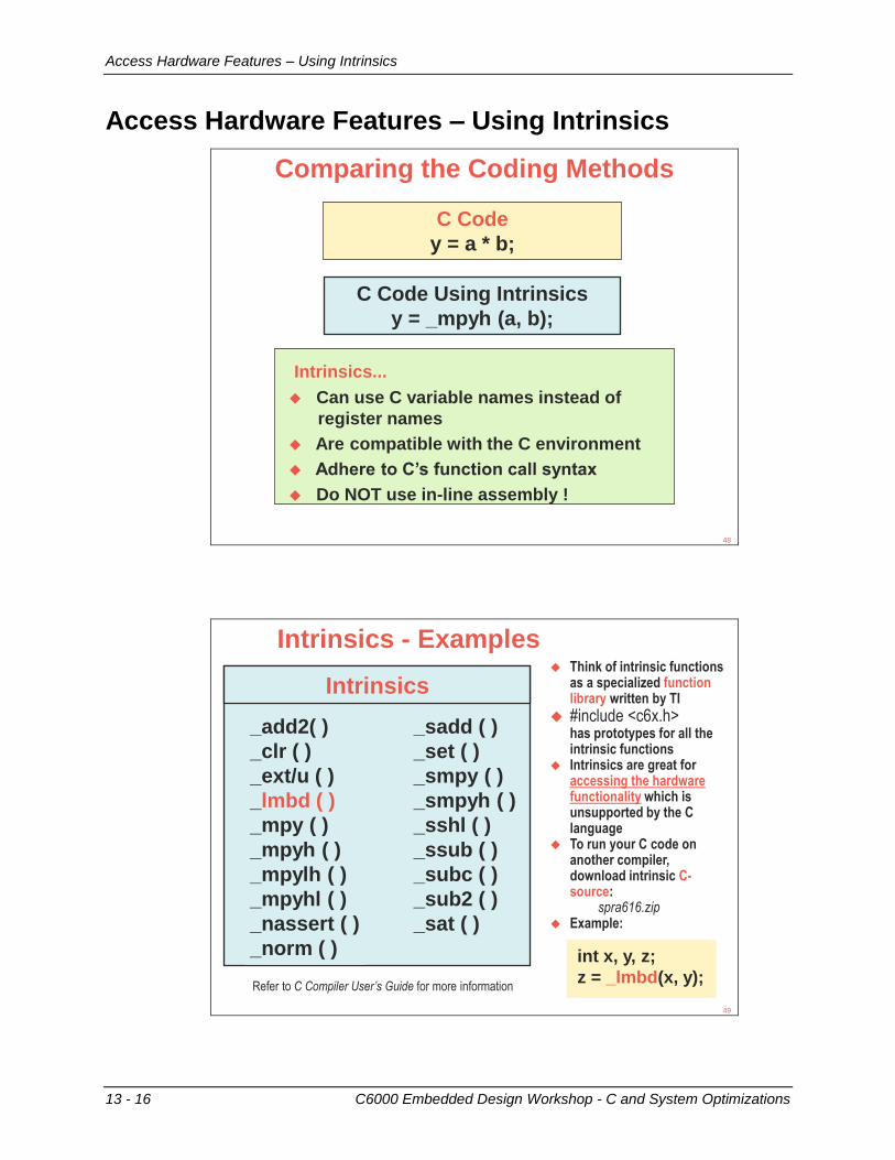
Access Hardware Features – Using Intrinsics
13 - 16 C6000 Embedded Design Workshop - C and System Optimizations
Access Hardware Features – Using Intrinsics
C Code
y = a * b;
C Code Using Intrinsics
y = _mpyh (a, b);
In-Line Assembly
asm (“ MPYH A0, A1, A2”);
Assembly Code
MPYH A0, A1, A2
Comparing the Coding Methods
Can use C variable names instead of
register names
Are compatible with the C environment
Adhere to C’s function call syntax
Do NOT use in-line assembly !
Intrinsics...
48
Intrinsics
_sadd ( )
_set ( )
_smpy ( )
_smpyh ( )
_sshl ( )
_ssub ( )
_subc ( )
_sub2 ( )
_sat ( )
_add2( )
_clr ( )
_ext/u ( )
_lmbd ( )
_mpy ( )
_mpyh ( )
_mpylh ( )
_mpyhl ( )
_nassert ( )
_norm ( )
Intrinsics - Examples Think of intrinsic functions
as a specialized function library written by TI
#include <c6x.h>has prototypes for all the intrinsic functions
Intrinsics are great for accessing the hardwarefunctionality which is unsupported by the C language
To run your C code on another compiler, download intrinsic C-source:
spra616.zip Example:
Refer to C Compiler User’s Guide for more information
int x, y, z;
z = _lmbd(x, y);
49
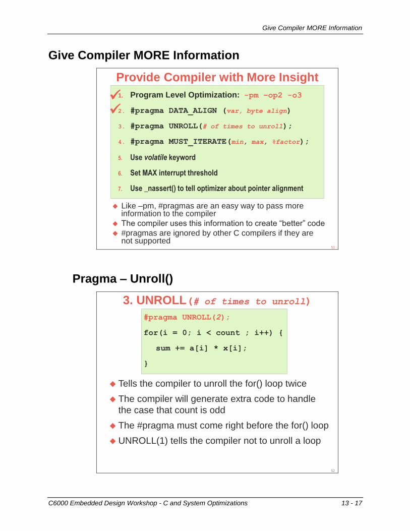
Give Compiler MORE Information
C6000 Embedded Design Workshop - C and System Optimizations 13 - 17
Give Compiler MORE Information
Provide Compiler with More Insight
1. Program Level Optimization: -pm –op2 -o3
2. #pragma DATA_ALIGN (var, byte align)
3. #pragma UNROLL(# of times to unroll);
4. #pragma MUST_ITERATE(min, max, %factor);
5. Use volatile keyword
6. Set MAX interrupt threshold
7. Use _nassert() to tell optimizer about pointer alignment
Like –pm, #pragmas are an easy way to pass moreinformation to the compiler
The compiler uses this information to create “better” code
#pragmas are ignored by other C compilers if they arenot supported
51
Pragma – Unroll()
3. UNROLL(# of times to unroll)
#pragma UNROLL(2);
for(i = 0; i < count ; i++) {
sum += a[i] * x[i];
}
Tells the compiler to unroll the for() loop twice
The compiler will generate extra code to handle
the case that count is odd
The #pragma must come right before the for() loop
UNROLL(1) tells the compiler not to unroll a loop
52
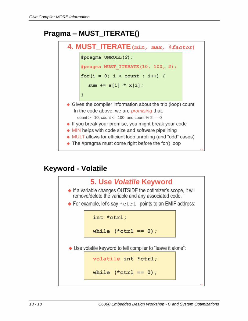
Give Compiler MORE Information
13 - 18 C6000 Embedded Design Workshop - C and System Optimizations
Pragma – MUST_ITERATE()
4. MUST_ITERATE(min, max, %factor)
#pragma UNROLL(2);
#pragma MUST_ITERATE(10, 100, 2);
for(i = 0; i < count ; i++) {
sum += a[i] * x[i];
}
Gives the compiler information about the trip (loop) count
In the code above, we are promising that:
count >= 10, count <= 100, and count % 2 == 0
If you break your promise, you might break your code
MIN helps with code size and software pipelining
MULT allows for efficient loop unrolling (and “odd” cases)
The #pragma must come right before the for() loop53
Keyword - Volatile
5. Use Volatile Keyword
int *ctrl;
while (*ctrl == 0);
volatile int *ctrl;
while (*ctrl == 0);
If a variable changes OUTSIDE the optimizer’s scope, it willremove/delete the variable and any associated code.
For example, let’s say *ctrl points to an EMIF address:
Use volatile keyword to tell compiler to “leave it alone”:
54
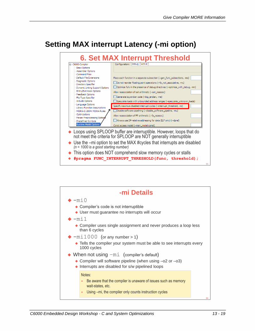
Give Compiler MORE Information
C6000 Embedded Design Workshop - C and System Optimizations 13 - 19
Setting MAX interrupt Latency (-mi option)
Loops using SPLOOP buffer are interruptible. However, loops that do not meet the criteria for SPLOOP are NOT generally interruptible
Use the –mi option to set the MAX #cycles that interrupts are disabled(n = 1000 is a good starting number)
This option does NOT comprehend slow memory cycles or stalls #pragma FUNC_INTERRUPT_THRESHOLD(func, threshold);
6. Set MAX Interrupt Threshold
55
-mi Details -mi0
Compiler’s code is not interruptible
User must guarantee no interrupts will occur
-mi1
Compiler uses single assignment and never produces a loop less than 6 cycles
-mi1000 (or any number > 1)
Tells the compiler your system must be able to see interrupts every 1000 cycles
When not using –mi (compiler’s default)
Compiler will software pipeline (when using –o2 or –o3)
Interrupts are disabled for s/w pipelined loops
Notes:
Be aware that the compiler is unaware of issues such as memory
wait-states, etc.
Using –mi, the compiler only counts instruction cycles
56
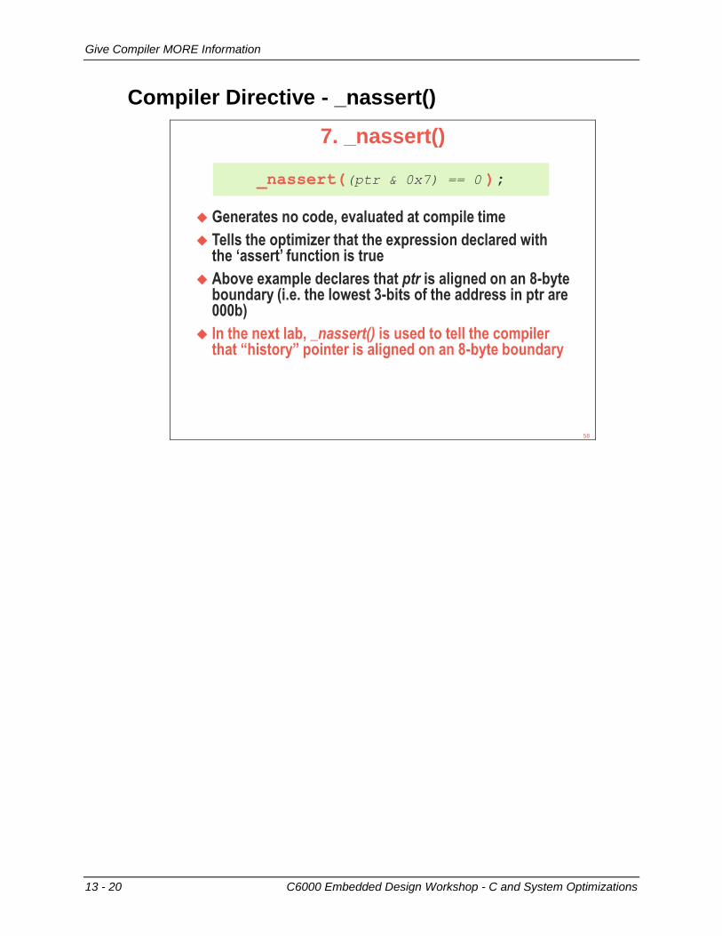
Give Compiler MORE Information
13 - 20 C6000 Embedded Design Workshop - C and System Optimizations
Compiler Directive - _nassert()
Generates no code, evaluated at compile time
Tells the optimizer that the expression declared with the ‘assert’ function is true
Above example declares that ptr is aligned on an 8-byte boundary (i.e. the lowest 3-bits of the address in ptr are 000b)
In the next lab, _nassert() is used to tell the compiler that “history” pointer is aligned on an 8-byte boundary
7. _nassert()
_nassert((ptr & 0x7) == 0 );
58
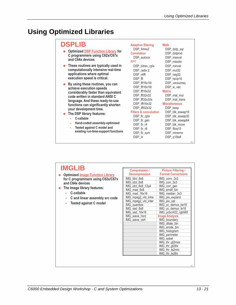
Using Optimized Libraries
C6000 Embedded Design Workshop - C and System Optimizations 13 - 21
Using Optimized Libraries
DSPLIB Optimized DSP Function Library for
C programmers using C62x/C67x and C64x devices
These routines are typically used in computationally intensive real-time applications where optimal execution speed is critical.
By using these routines, you can achieve execution speeds considerably faster than equivalent code written in standard ANSI C language. And these ready-to-use functions can significantly shorten your development time.
The DSP library features:
C-callable
Hand-coded assembly-optimized
Tested against C model and existing run-time-support functions
Adaptive filtering Math
DSP_firlms2 DSP_dotp_sqr
Correlation DSP_dotprod
DSP_autocor DSP_maxval
FFT DSP_maxidx
DSP_bitrev_cplx DSP_minval
DSP_radix 2 DSP_mul32
DSP_r4fft DSP_neg32
DSP_fft DSP_recip16
DSP_fft16x16r DSP_vecsumsq
DSP_fft16x16t DSP_w_vec
DSP_fft16x32 Matrix
DSP_fft32x32 DSP_mat_mul
DSP_fft32x32s DSP_mat_trans
DSP_ifft16x32 Miscellaneous
DSP_ifft32x32 DSP_bexp
Filters & convolution DSP_blk_eswap16
DSP_fir_cplx DSP_blk_eswap32
DSP_fir_gen DSP_blk_eswap64
DSP_fir_r4 DSP_blk_move
DSP_fir_r8 DSP_fltoq15
DSP_fir_sym DSP_minerror
DSP_iir DSP_q15tofl
60
IMGLIB Optimized Image Function Library
for C programmers using C62x/C67x and C64x devices
The Image library features:
C-callable
C and linear assembly src code
Tested against C model
Compression / Decompression
Picture Filtering / Format Conversions
IMG_fdct_8x8 IMG_conv_3x3 IMG_idct_8x8 IMG_corr_3x3IMG_idct_8x8_12q4 IMG_corr_gen IMG_mad_8x8 IMG_errdif_bin IMG_mad_16x16 IMG_median_3x3 IMG_mpeg2_vld_intra IMG_pix_expand IMG_mpeg2_vld_inter IMG_pix_sat IMG_quantize IMG_yc_demux_be16 IMG_sad_8x8 IMG_yc_demux_le16 IMG_sad_16x16 IMG_ycbcr422_rgb565 IMG_wave_horz Image AnalysisIMG_wave_vert IMG_boundary
IMG_dilate_bin IMG_erode_bin IMG_histogram IMG_perimeter IMG_sobel IMG_thr_gt2max IMG_thr_gt2thr IMG_thr_le2min IMG_thr_le2thr
61
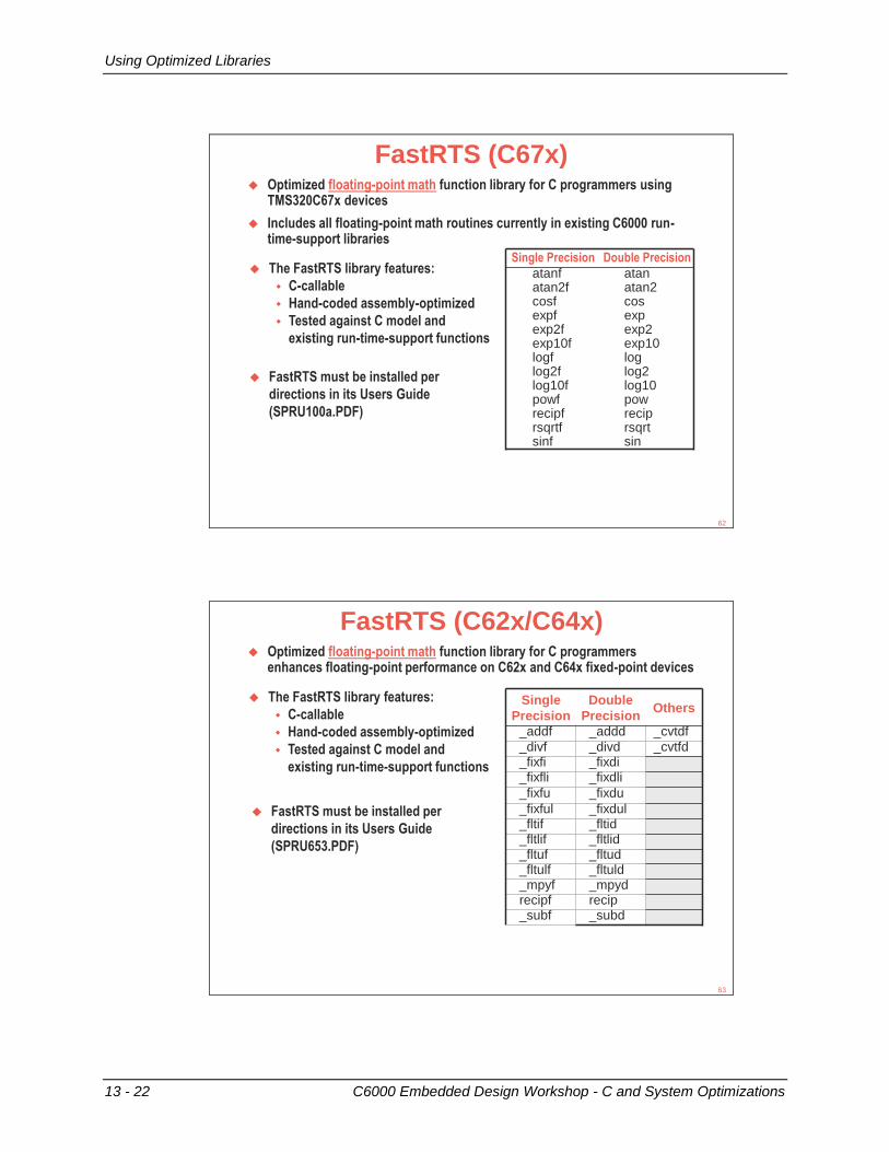
Using Optimized Libraries
13 - 22 C6000 Embedded Design Workshop - C and System Optimizations
FastRTS (C67x) Optimized floating-point math function library for C programmers using
TMS320C67x devices
Includes all floating-point math routines currently in existing C6000 run-time-support libraries
Single Precision Double Precision
atanf atanatan2f atan2cosf cosexpf expexp2f exp2exp10f exp10logf loglog2f log2log10f log10powf powrecipf reciprsqrtf rsqrtsinf sin
The FastRTS library features:
C-callable
Hand-coded assembly-optimized
Tested against C model and
existing run-time-support functions
FastRTS must be installed per
directions in its Users Guide
(SPRU100a.PDF)
62
FastRTS (C62x/C64x) Optimized floating-point math function library for C programmers
enhances floating-point performance on C62x and C64x fixed-point devices
The FastRTS library features:
C-callable
Hand-coded assembly-optimized
Tested against C model and
existing run-time-support functions
FastRTS must be installed per
directions in its Users Guide
(SPRU653.PDF)
Single
Precision
Double
PrecisionOthers
_addf _addd _cvtdf
_divf _divd _cvtfd_fixfi _fixdi_fixfli _fixdli
_fixfu _fixdu
_fixful _fixdul_fltif _fltid_fltlif _fltlid_fltuf _fltud_fltulf _fltuld_mpyf _mpydrecipf recip_subf _subd
63
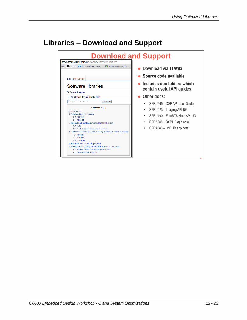
Using Optimized Libraries
C6000 Embedded Design Workshop - C and System Optimizations 13 - 23
Libraries – Download and Support
Download and Support
Download via TI Wiki
Source code available
Includes doc folders which contain useful API guides
Other docs:
• SPRU565 – DSP API User Guide
• SPRU023 – Imaging API UG
• SPRU100 – FastRTS Math API UG
• SPRA885 – DSPLIB app note
• SPRA886 – IMGLIB app note
64
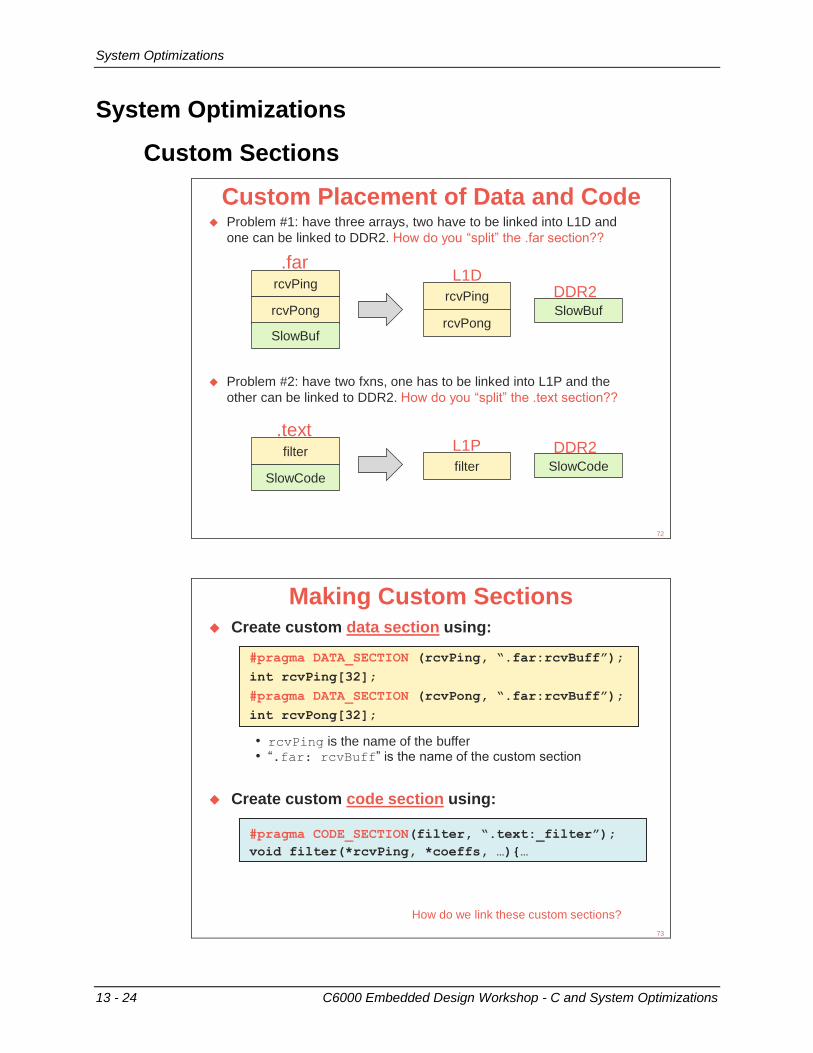
System Optimizations
13 - 24 C6000 Embedded Design Workshop - C and System Optimizations
System Optimizations
Custom Sections
Custom Placement of Data and Code Problem #1: have three arrays, two have to be linked into L1D and
one can be linked to DDR2. How do you “split” the .far section??
rcvPing
rcvPong
SlowBuf
.far
rcvPing
rcvPongSlowBuf
L1DDDR2
Problem #2: have two fxns, one has to be linked into L1P and the
other can be linked to DDR2. How do you “split” the .text section??
filter
SlowCode
.text
filter SlowCode
L1P DDR2
72
Making Custom Sections
#pragma DATA_SECTION (rcvPing, “.far:rcvBuff”);
int rcvPing[32];
#pragma DATA_SECTION (rcvPong, “.far:rcvBuff”);
int rcvPong[32];
Create custom data section using:
#pragma CODE_SECTION(filter, “.text:_filter”);
void filter(*rcvPing, *coeffs, …){…
Create custom code section using:
How do we link these custom sections?
• rcvPing is the name of the buffer• “.far: rcvBuff” is the name of the custom section
73
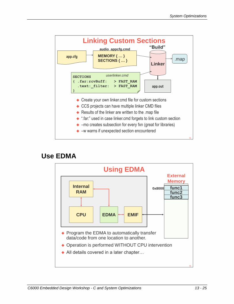
System Optimizations
C6000 Embedded Design Workshop - C and System Optimizations 13 - 25
Linking Custom Sections
app.cfg
Linker
app.out
Create your own linker.cmd file for custom sections
CCS projects can have multiple linker CMD files
Results of the linker are written to the .map file
“.far:” used in case linker.cmd forgets to link custom section
–mo creates subsection for every fxn (great for libraries)
–w warns if unexpected section encountered
“Build”
SECTIONS
{ .far:rcvBuff: > FAST_RAM
.text:_filter: > FAST_RAM
}
MEMORY { … }
SECTIONS { … }
audio_appcfg.cmd
.map
userlinker.cmd
74
Use EDMA
CPU
Internal
RAM
EDMA
Using EDMAExternal
Memory
EMIF
Programfunc1func2func3
0x8000
Program the EDMA to automatically transferdata/code from one location to another.
Operation is performed WITHOUT CPU intervention
All details covered in a later chapter…
76
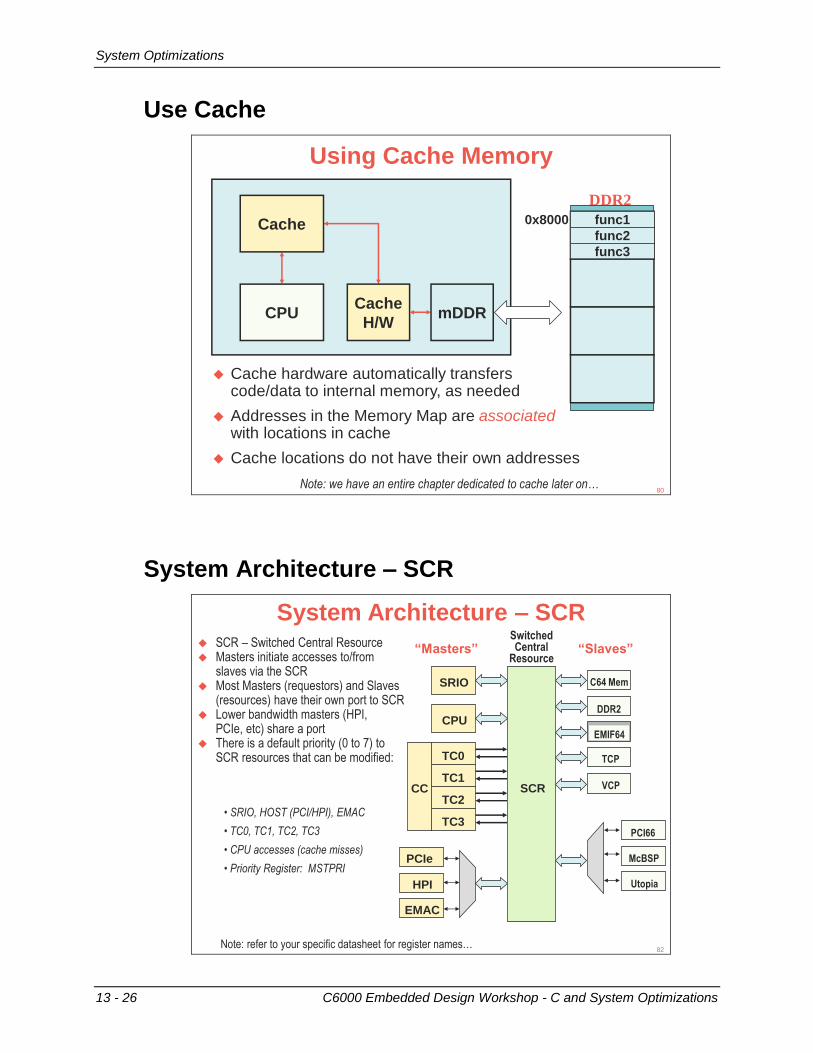
System Optimizations
13 - 26 C6000 Embedded Design Workshop - C and System Optimizations
Use Cache
CPU
Cache
Cache
H/W
Using Cache Memory
DDR2
mDDR
Programfunc1
func2
func3
0x8000
Cache hardware automatically transfers code/data to internal memory, as needed
Addresses in the Memory Map are associatedwith locations in cache
Cache locations do not have their own addresses
Note: we have an entire chapter dedicated to cache later on…80
System Architecture – SCR
System Architecture – SCR
SRIO
CPU
TC0
TC1
TC2
TC3
CC
PCIe
HPI
EMAC
SCR
SwitchedCentral
Resource
C64 Mem
DDR2
EMIF64
TCP
VCP
PCI66
McBSP
Utopia
“Masters” “Slaves” SCR – Switched Central Resource Masters initiate accesses to/from
slaves via the SCR Most Masters (requestors) and Slaves
(resources) have their own port to SCR Lower bandwidth masters (HPI,
PCIe, etc) share a port There is a default priority (0 to 7) to
SCR resources that can be modified:
• SRIO, HOST (PCI/HPI), EMAC
• TC0, TC1, TC2, TC3
• CPU accesses (cache misses)
• Priority Register: MSTPRI
Note: refer to your specific datasheet for register names…82
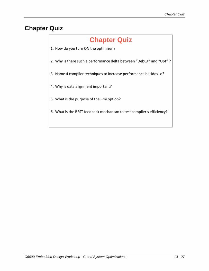
Chapter Quiz
C6000 Embedded Design Workshop - C and System Optimizations 13 - 27
Chapter Quiz
Chapter Quiz1. How do you turn ON the optimizer ?
2. Why is there such a performance delta between “Debug” and “Opt” ?
3. Name 4 compiler techniques to increase performance besides -o?
4. Why is data alignment important?
5. What is the purpose of the –mi option?
6. What is the BEST feedback mechanism to test compiler’s efficiency?
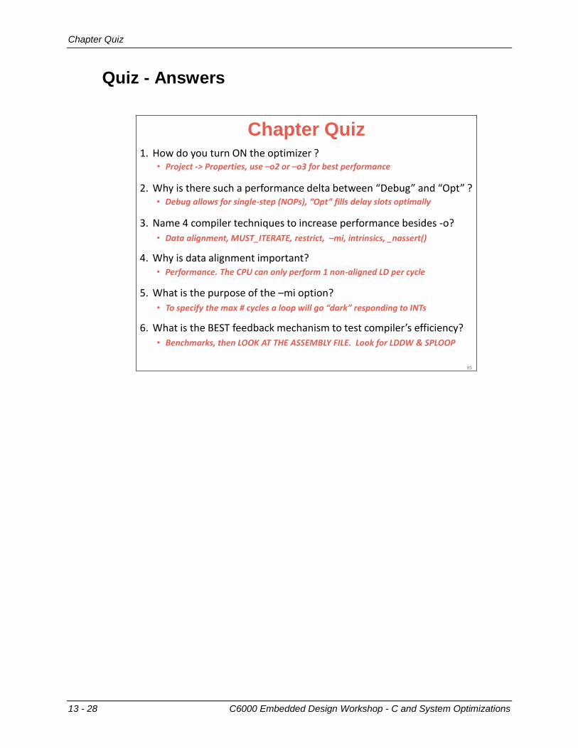
Chapter Quiz
13 - 28 C6000 Embedded Design Workshop - C and System Optimizations
Quiz - Answers
Chapter Quiz1. How do you turn ON the optimizer ?
2. Why is there such a performance delta between “Debug” and “Opt” ?
3. Name 4 compiler techniques to increase performance besides -o?
4. Why is data alignment important?
5. What is the purpose of the –mi option?
6. What is the BEST feedback mechanism to test compiler’s efficiency?
• Project -> Properties, use –o2 or –o3 for best performance
• Debug allows for single-step (NOPs), “Opt” fills delay slots optimally
• Data alignment, MUST_ITERATE, restrict, –mi, intrinsics, _nassert()
• To specify the max # cycles a loop will go “dark” responding to INTs
• Performance. The CPU can only perform 1 non-aligned LD per cycle
• Benchmarks, then LOOK AT THE ASSEMBLY FILE. Look for LDDW & SPLOOP
85
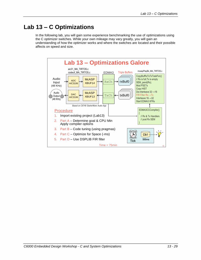
Lab 13 – C Optimizations
C6000 Embedded Design Workshop - C and System Optimizations 13 - 29
Lab 13 – C Optimizations
In the following lab, you will gain some experience benchmarking the use of optimizations using the C optimizer switches. While your own mileage may vary greatly, you will gain an understanding of how the optimizer works and where the switches are located and their possible affects on speed and size.
Audio
Output
(48 KHz)
Lab 13 – Optimizations Galore
ADC
AIC3106
Audio
Input (48 KHz)
McASP
XBUF14
DAC
AIC3106
McASP
XBUF13
1. Import existing project (Lab13)
2. Part A – Determine goal & CPU MinApply compiler options
3. Part B – Code tuning (using pragmas)
4. Part C – Optimize for Space (-ms)
5. Part D – Use DSPLIB FIR filter
aic31_MA_TIRTOS.c
codecif_MA_TIRTOS.cmcaspPlayBk_MA_TIRTOS.c
rxBuf0rxBuf0rxBuf0
Triple Buffers
Time = 75min
Procedure
49
txBuf0txBuf0txBuf0
EDMA3
RxCh
TxCh
CopyBufRxToTxTaskFxn()
// Rx is full,Tx is empty
SEM_pend(Rx);
Mod PSETs
Copy HIST
De-interleave 32→16
FIR Filter Rx→Tx
Interleave 16→32
Start EDMA3 XFRs
EDMA3CCComplIsr()
{
// Rx & Tx Handlers
// post Rx SEM
}
Based on C6748 StarterWare Audio App
Clk1
Tick500ms
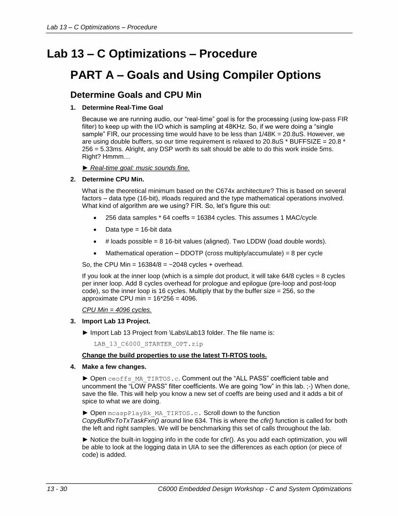
Lab 13 – C Optimizations – Procedure
13 - 30 C6000 Embedded Design Workshop - C and System Optimizations
Lab 13 – C Optimizations – Procedure
PART A – Goals and Using Compiler Options
Determine Goals and CPU Min
1. Determine Real-Time Goal
Because we are running audio, our “real-time” goal is for the processing (using low-pass FIR filter) to keep up with the I/O which is sampling at 48KHz. So, if we were doing a “single sample” FIR, our processing time would have to be less than 1/48K = 20.8uS. However, we are using double buffers, so our time requirement is relaxed to 20.8uS * BUFFSIZE = 20.8 * 256 = 5.33ms. Alright, any DSP worth its salt should be able to do this work inside 5ms. Right? Hmmm…
► Real-time goal: music sounds fine.
2. Determine CPU Min.
What is the theoretical minimum based on the C674x architecture? This is based on several factors – data type (16-bit), #loads required and the type mathematical operations involved. What kind of algorithm are we using? FIR. So, let’s figure this out:
256 data samples * 64 coeffs = 16384 cycles. This assumes 1 MAC/cycle
Data type = 16-bit data
# loads possible = 8 16-bit values (aligned). Two LDDW (load double words).
Mathematical operation – DDOTP (cross multiply/accumulate) = 8 per cycle
So, the CPU Min = 16384/8 = ~2048 cycles + overhead.
If you look at the inner loop (which is a simple dot product, it will take 64/8 cycles = 8 cycles per inner loop. Add 8 cycles overhead for prologue and epilogue (pre-loop and post-loop code), so the inner loop is 16 cycles. Multiply that by the buffer size = 256, so the approximate CPU min = 16*256 = 4096.
CPU Min = 4096 cycles.
3. Import Lab 13 Project.
► Import Lab 13 Project from \Labs\Lab13 folder. The file name is:
LAB_13_C6000_STARTER_OPT.zip
Change the build properties to use the latest TI-RTOS tools.
4. Make a few changes.
► Open ceoffs_MA_TIRTOS.c. Comment out the “ALL PASS” coefficient table and
uncomment the “LOW PASS” filter coefficients. We are going “low” in this lab. ;-) When done, save the file. This will help you know a new set of coeffs are being used and it adds a bit of spice to what we are doing.
► Open mcaspPlayBk_MA_TIRTOS.c. Scroll down to the function
CopyBufRxToTxTaskFxn() around line 634. This is where the cfir() function is called for both the left and right samples. We will be benchmarking this set of calls throughout the lab.
► Notice the built-in logging info in the code for cfir(). As you add each optimization, you will be able to look at the logging data in UIA to see the differences as each option (or piece of code) is added.
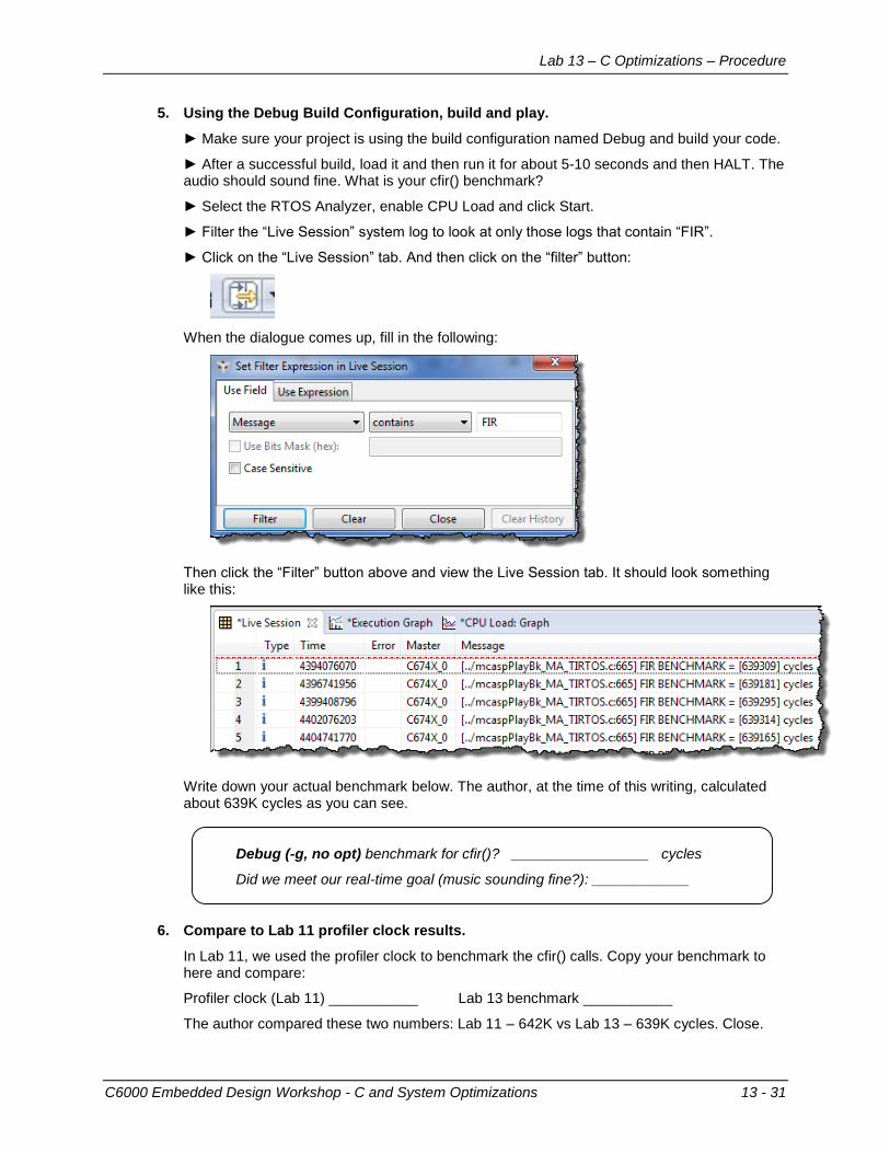
Lab 13 – C Optimizations – Procedure
C6000 Embedded Design Workshop - C and System Optimizations 13 - 31
5. Using the Debug Build Configuration, build and play.
► Make sure your project is using the build configuration named Debug and build your code.
► After a successful build, load it and then run it for about 5-10 seconds and then HALT. The audio should sound fine. What is your cfir() benchmark?
► Select the RTOS Analyzer, enable CPU Load and click Start.
► Filter the “Live Session” system log to look at only those logs that contain “FIR”.
► Click on the “Live Session” tab. And then click on the “filter” button:
When the dialogue comes up, fill in the following:
Then click the “Filter” button above and view the Live Session tab. It should look something like this:
Write down your actual benchmark below. The author, at the time of this writing, calculated about 639K cycles as you can see.
Debug (-g, no opt) benchmark for cfir()? _________________ cycles
Did we meet our real-time goal (music sounding fine?): ____________
6. Compare to Lab 11 profiler clock results.
In Lab 11, we used the profiler clock to benchmark the cfir() calls. Copy your benchmark to here and compare:
Profiler clock (Lab 11) ___________ Lab 13 benchmark ___________
The author compared these two numbers: Lab 11 – 642K vs Lab 13 – 639K cycles. Close.
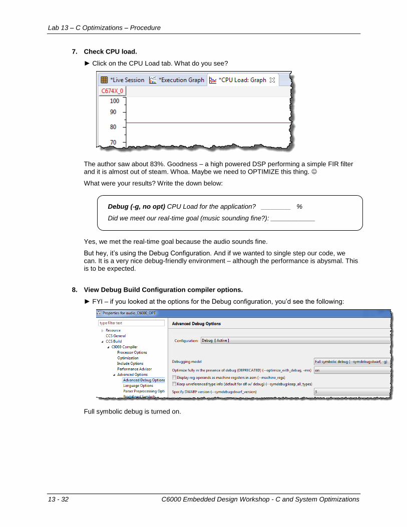
Lab 13 – C Optimizations – Procedure
13 - 32 C6000 Embedded Design Workshop - C and System Optimizations
7. Check CPU load.
► Click on the CPU Load tab. What do you see?
The author saw about 83%. Goodness – a high powered DSP performing a simple FIR filter and it is almost out of steam. Whoa. Maybe we need to OPTIMIZE this thing.
What were your results? Write the down below:
Debug (-g, no opt) CPU Load for the application? ________ %
Did we meet our real-time goal (music sounding fine?): ____________
Yes, we met the real-time goal because the audio sounds fine.
But hey, it’s using the Debug Configuration. And if we wanted to single step our code, we can. It is a very nice debug-friendly environment – although the performance is abysmal. This is to be expected.
8. View Debug Build Configuration compiler options.
► FYI – if you looked at the options for the Debug configuration, you’d see the following:
Full symbolic debug is turned on.
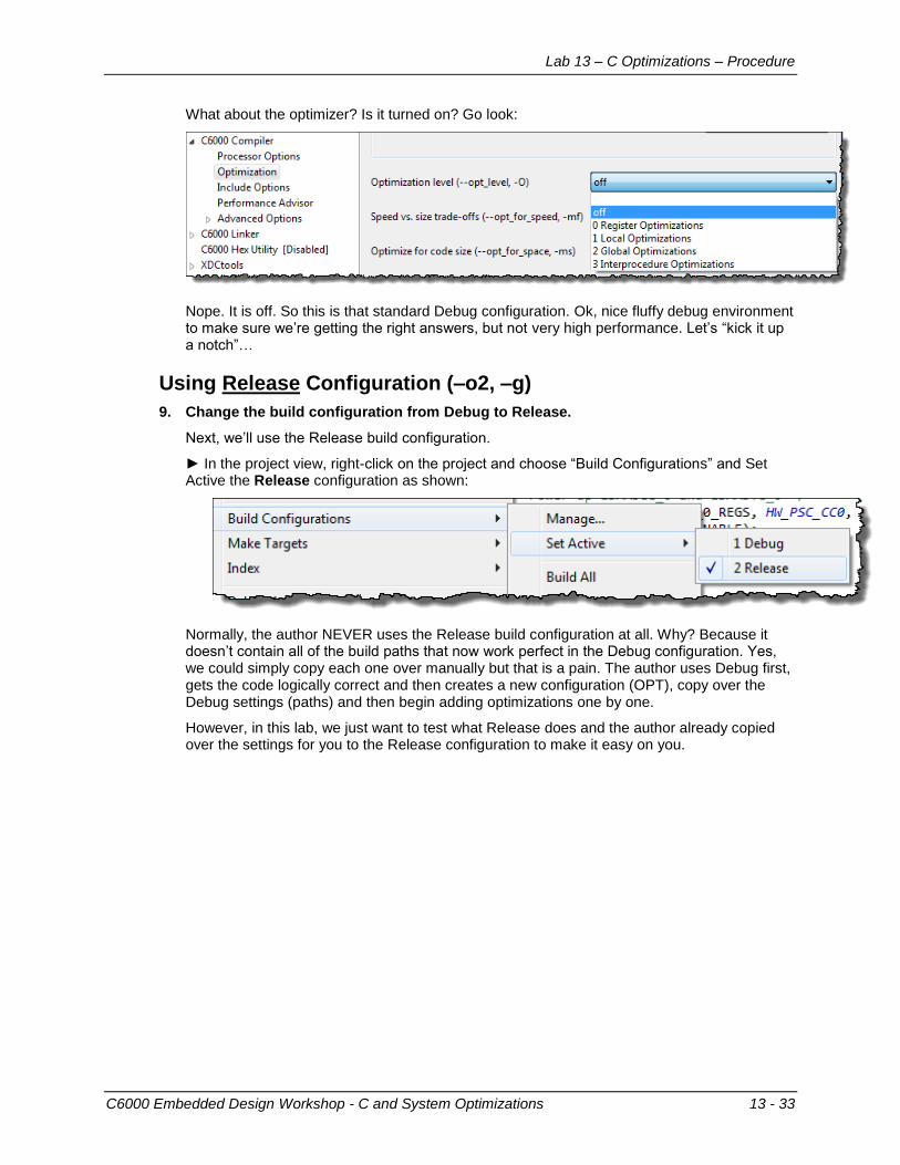
Lab 13 – C Optimizations – Procedure
C6000 Embedded Design Workshop - C and System Optimizations 13 - 33
What about the optimizer? Is it turned on? Go look:
Nope. It is off. So this is that standard Debug configuration. Ok, nice fluffy debug environment to make sure we’re getting the right answers, but not very high performance. Let’s “kick it up a notch”…
Using Release Configuration (–o2, –g)
9. Change the build configuration from Debug to Release.
Next, we’ll use the Release build configuration.
► In the project view, right-click on the project and choose “Build Configurations” and Set Active the Release configuration as shown:
Normally, the author NEVER uses the Release build configuration at all. Why? Because it doesn’t contain all of the build paths that now work perfect in the Debug configuration. Yes, we could simply copy each one over manually but that is a pain. The author uses Debug first, gets the code logically correct and then creates a new configuration (OPT), copy over the Debug settings (paths) and then begin adding optimizations one by one.
However, in this lab, we just want to test what Release does and the author already copied over the settings for you to the Release configuration to make it easy on you.
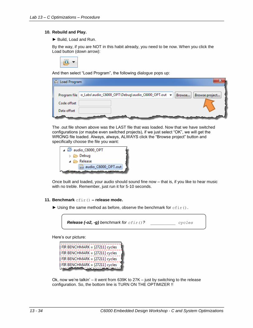
Lab 13 – C Optimizations – Procedure
13 - 34 C6000 Embedded Design Workshop - C and System Optimizations
10. Rebuild and Play.
► Build, Load and Run.
By the way, if you are NOT in this habit already, you need to be now. When you click the Load button (down arrow):
And then select “Load Program”, the following dialogue pops up:
The .out file shown above was the LAST file that was loaded. Now that we have switched configurations (or maybe even switched projects), if we just select “OK”, we will get the WRONG file loaded. Always, always, ALWAYS click the “Browse project” button and specifically choose the file you want:
Once built and loaded, your audio should sound fine now – that is, if you like to hear music with no treble. Remember, just run it for 5-10 seconds.
11. Benchmark cfir() – release mode.
► Using the same method as before, observe the benchmark for cfir().
Release (-o2, -g) benchmark for cfir()? __________ cycles
Here’s our picture:
Ok, now we’re talkin’ – it went from 639K to 27K – just by switching to the release configuration. So, the bottom line is TURN ON THE OPTIMIZER !!
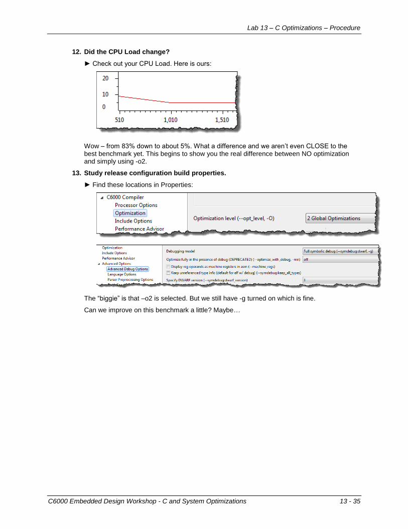
Lab 13 – C Optimizations – Procedure
C6000 Embedded Design Workshop - C and System Optimizations 13 - 35
12. Did the CPU Load change?
► Check out your CPU Load. Here is ours:
Wow – from 83% down to about 5%. What a difference and we aren’t even CLOSE to the best benchmark yet. This begins to show you the real difference between NO optimization and simply using -o2.
13. Study release configuration build properties.
► Find these locations in Properties:
The “biggie” is that –o2 is selected. But we still have -g turned on which is fine.
Can we improve on this benchmark a little? Maybe…
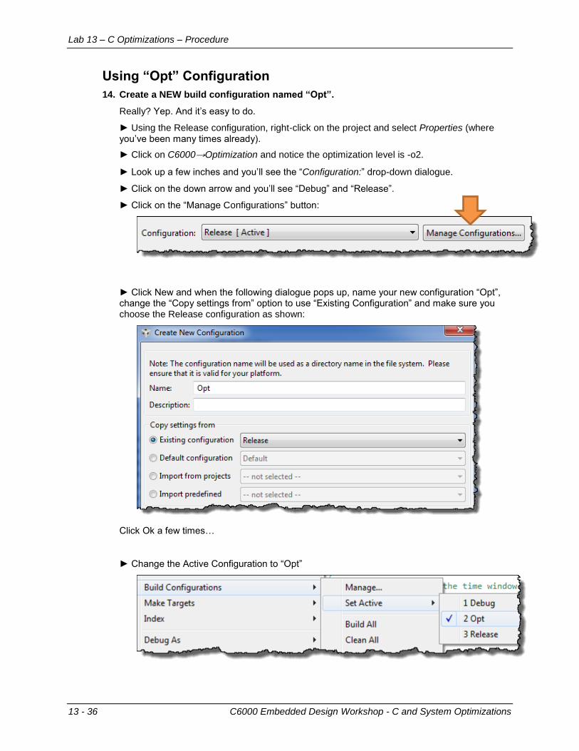
Lab 13 – C Optimizations – Procedure
13 - 36 C6000 Embedded Design Workshop - C and System Optimizations
Using “Opt” Configuration
14. Create a NEW build configuration named “Opt”.
Really? Yep. And it’s easy to do.
► Using the Release configuration, right-click on the project and select Properties (where you’ve been many times already).
► Click on C6000→Optimization and notice the optimization level is -o2.
► Look up a few inches and you’ll see the “Configuration:” drop-down dialogue.
► Click on the down arrow and you’ll see “Debug” and “Release”.
► Click on the “Manage Configurations” button:
► Click New and when the following dialogue pops up, name your new configuration “Opt”, change the “Copy settings from” option to use “Existing Configuration” and make sure you choose the Release configuration as shown:
Click Ok a few times…
► Change the Active Configuration to “Opt”
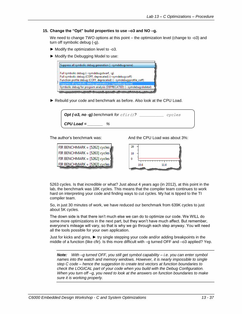
Lab 13 – C Optimizations – Procedure
C6000 Embedded Design Workshop - C and System Optimizations 13 - 37
15. Change the “Opt” build properties to use –o3 and NO –g.
We need to change TWO options at this point – the optimization level (change to -o3) and turn off symbolic debug (-g).
► Modify the optimization level to -o3.
► Modify the Debugging Model to use:
► Rebuild your code and benchmark as before. Also look at the CPU Load.
Opt (-o3, no -g) benchmark for cfir()? ___________ cycles
CPU Load = _______ %
The author’s benchmark was: And the CPU Load was about 3%:
5263 cycles. Is that incredible or what? Just about 4 years ago (in 2012), at this point in the lab, the benchmark was 18K cycles. This means that the compiler team continues to work hard on interpreting your code and finding ways to cut cycles. My hat is tipped to the TI compiler team.
So, in just 30 minutes of work, we have reduced our benchmark from 639K cycles to just about 5K cycles.
The down side is that there isn’t much else we can do to optimize our code. We WILL do some more optimizations in the next part, but they won’t have much affect. But remember, everyone’s mileage will vary, so that is why we go through each step anyway. You will need all the tools possible for your own application.
Just for kicks and grins, ► try single stepping your code and/or adding breakpoints in the middle of a function (like cfir). Is this more difficult with –g turned OFF and –o3 applied? Yep.
Note: With –g turned OFF, you still get symbol capability – i.e. you can enter symbol names into the watch and memory windows. However, it is nearly impossible to single step C code – hence the suggestion to create test vectors at function boundaries to check the LOGICAL part of your code when you build with the Debug Configuration. When you turn off –g, you need to look at the answers on function boundaries to make
sure it is working properly.
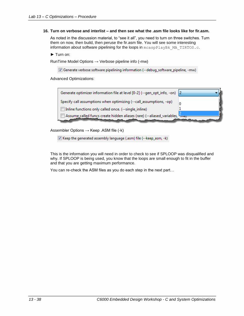
Lab 13 – C Optimizations – Procedure
13 - 38 C6000 Embedded Design Workshop - C and System Optimizations
16. Turn on verbose and interlist – and then see what the .asm file looks like for fir.asm.
As noted in the discussion material, to “see it all”, you need to turn on three switches. Turn them on now, then build, then peruse the fir.asm file. You will see some interesting
information about software pipelining for the loops in mcaspPlayBk_MA_TIRTOS.c.
► Turn on:
RunTime Model Options → Verbose pipeline info (-mw)
Advanced Optimizations:
Assembler Options → Keep .ASM file (-k)
This is the information you will need in order to check to see if SPLOOP was disqualified and why. If SPLOOP is being used, you know that the loops are small enough to fit in the buffer and that you are getting maximum performance.
You can re-check the ASM files as you do each step in the next part…
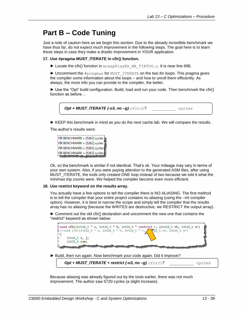
Lab 13 – C Optimizations – Procedure
C6000 Embedded Design Workshop - C and System Optimizations 13 - 39
Part B – Code Tuning
Just a note of caution here as we begin this section. Due to the already incredible benchmark we have thus far, do not expect much improvement in the following steps. The goal here is to learn these steps in case they make a drastic improvement in YOUR application.
17. Use #pragma MUST_ITERATE in cfir() function.
► Locate the cfir() function in mcaspPlayBk_MA_TIRTOS.c. It is near line 696.
► Uncomment the #pragmas for MUST_ITERATE on the two for loops. This pragma gives
the compiler some information about the loops – and how to unroll them efficiently. As always, the more info you can provide to the compiler, the better.
► Use the “Opt” build configuration. Build, load and run your code. Then benchmark the cfir() function as before…
Opt + MUST_ITERATE (-o3, no –g) cfir()? __________ cycles
► KEEP this benchmark in mind as you do the next cache lab. We will compare the results.
The author’s results were:
Ok, so the benchmark is similar if not identical. That’s ok. Your mileage may vary in terms of your own system. Also, if you were paying attention to the generated ASM files, after using MUST_ITERATE, the tools only created ONE loop instead of two because we told it what the min/max trip counts were. We helped the compiler become even more efficient.
18. Use restrict keyword on the results array.
You actually have a few options to tell the compiler there is NO ALIASING. The first method is to tell the compiler that your entire project contains no aliasing (using the –mt compiler option). However, it is best to narrow the scope and simply tell the compiler that the results array has no aliasing (because the WRITES are destructive, we RESTRICT the output array).
► Comment out the old cfir() declaration and uncomment the new one that contains the “restrict” keyword as shown below:
► Build, then run again. Now benchmark your code again. Did it improve?
Opt + MUST_ITERATE + restrict (-o3, no –g) cfir()? __________ cycles
Because aliasing was already figured out by the tools earlier, there was not much improvement. The author saw 5720 cycles (a slight increase).
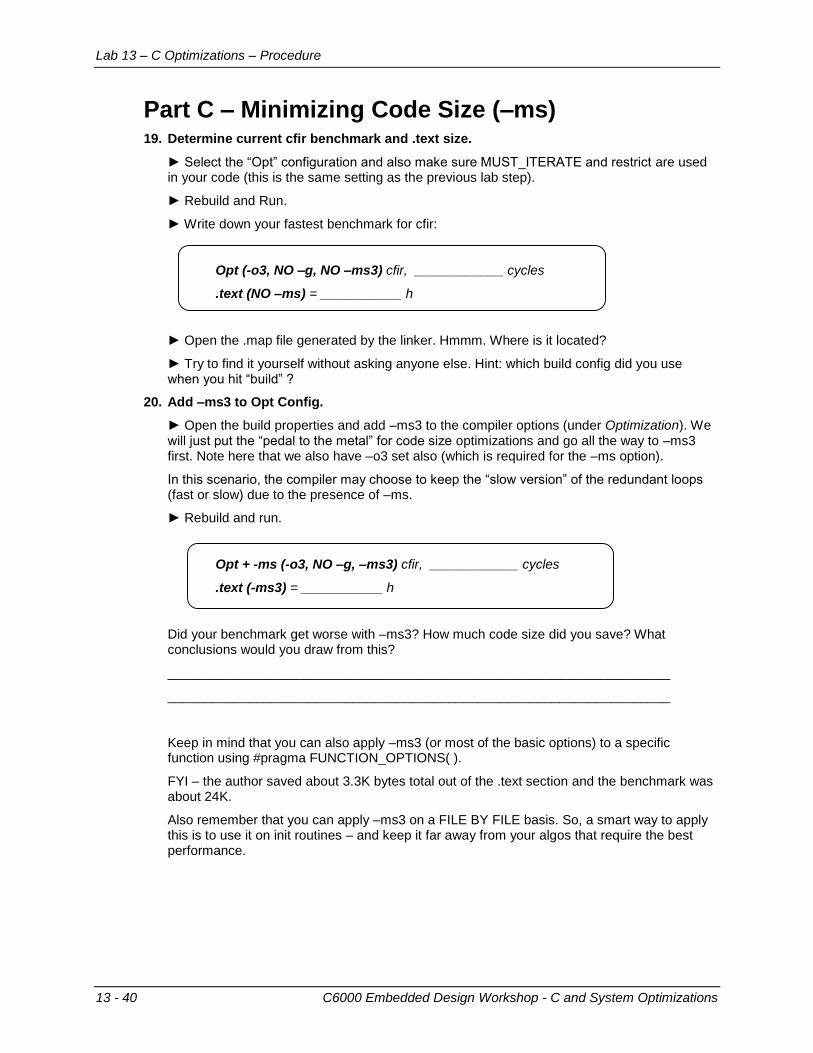
Lab 13 – C Optimizations – Procedure
13 - 40 C6000 Embedded Design Workshop - C and System Optimizations
Part C – Minimizing Code Size (–ms) 19. Determine current cfir benchmark and .text size.
► Select the “Opt” configuration and also make sure MUST_ITERATE and restrict are used in your code (this is the same setting as the previous lab step).
► Rebuild and Run.
► Write down your fastest benchmark for cfir:
Opt (-o3, NO –g, NO –ms3) cfir, ____________ cycles
.text (NO –ms) = ___________ h
► Open the .map file generated by the linker. Hmmm. Where is it located?
► Try to find it yourself without asking anyone else. Hint: which build config did you use when you hit “build” ?
20. Add –ms3 to Opt Config.
► Open the build properties and add –ms3 to the compiler options (under Optimization). We will just put the “pedal to the metal” for code size optimizations and go all the way to –ms3 first. Note here that we also have –o3 set also (which is required for the –ms option).
In this scenario, the compiler may choose to keep the “slow version” of the redundant loops (fast or slow) due to the presence of –ms.
► Rebuild and run.
Opt + -ms (-o3, NO –g, –ms3) cfir, ____________ cycles
.text (-ms3) = ___________ h
Did your benchmark get worse with –ms3? How much code size did you save? What conclusions would you draw from this?
____________________________________________________________________
____________________________________________________________________
Keep in mind that you can also apply –ms3 (or most of the basic options) to a specific function using #pragma FUNCTION_OPTIONS( ).
FYI – the author saved about 3.3K bytes total out of the .text section and the benchmark was about 24K.
Also remember that you can apply –ms3 on a FILE BY FILE basis. So, a smart way to apply this is to use it on init routines – and keep it far away from your algos that require the best performance.
Lab 13 – C Optimizations – Procedure
C6000 Embedded Design Workshop - C and System Optimizations 13 - 41
Part D – Using DSPLib
I will be interesting to test the C compiler’s best performance vs the DSPLib version of the FIR filter – which was hand-optimized in assembly. Of course, the assembly can’t be “optimized” and take advantage of the latest compiler upgrades. At one point in 2012, the compiler and the DSPLib benchmarks were almost identical. Let’s see how they compare today…
21. Download and install the appropriate DSP Library.
This, fortunately for you, has already been done for you. This directory is located at:
C:\TI_RTOS\C6000\dsplib64x+\lib\dsplib64plus_elf.lib
22. Link the appropriate library to your project.
► Find the lib file in the above folder and link it to your project (ELF version).
► Also, add the include path for this library to your build properties.
23. Add #include to the system_MA_TIRTOS.h file.
► Add the proper #include for the header file for this library to system_MA_TIRTOS.h.
24. Replace the calls to the fir function in fir.c.
► Replace:
cfir(rxBufFirL.hist, COEFFS, txBufFirL, ORDER, NUM_SAMPLES_PER_AUDIO_BUF/2);
cfir(rxBufFirR.hist, COEFFS, txBufFirR, ORDER, NUM_SAMPLES_PER_AUDIO_BUF/2);
with
DSP_fir_gen(rxBufFirL.hist, COEFFS, txBufFirL, ORDER,
NUM_SAMPLES_PER_AUDIO_BUF/2);
DSP_fir_gen(rxBufFirR.hist, COEFFS, txBufFirR, ORDER,
NUM_SAMPLES_PER_AUDIO_BUF/2);
25. Build, load, verify and BENCHMARK the new FIR routine in DSPLib.
26. What are the best-case benchmarks?
Yours (compiler/optimizer):___________ DSPLib: ___________
The author’s results are here:
Wow, for what we wanted in THIS system (a fast simple FIR routine), we would have been better off just using DSPLib. Yep. But, in the process, you’ve learned a great deal about optimization techniques across the board that may or may not help your specific system. Remember, your mileage may vary.
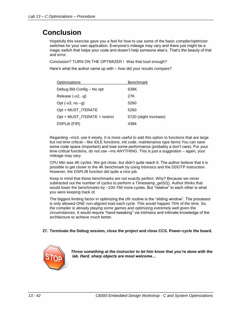
Lab 13 – C Optimizations – Procedure
13 - 42 C6000 Embedded Design Workshop - C and System Optimizations
Conclusion Hopefully this exercise gave you a feel for how to use some of the basic compiler/optimizer
switches for your own application. Everyone’s mileage may vary and there just might be a magic switch that helps your code and dosen’t help someone else’s. That’s the beauty of trial and error.
Conclusion? TURN ON THE OPTIMIZER ! Was that loud enough?
Here’s what the author came up with – how did your results compare?
Optimizations Benchmark
Debug Bld Config – No opt 639K
Release (-o2, -g) 27K
Opt (-o3, no –g) 5260
Opt + MUST_ITERATE 5260
Opt + MUST_ITERATE + restrict 5720 (slight increase)
DSPLib (FIR) 4384
Regarding –ms3, use it wisely. It is more useful to add this option to functions that are large but not time critical – like IDLE functions, init code, maintenance type items.You can save some code space (important) and lose some performance (probably a don’t care). For your time-critical functions, do not use –ms ANYTHING. This is just a suggestion – again, your mileage may vary.
CPU Min was 4K cycles. We got close, but didn’t quite reach it. The author believe that it is possible to get closer to the 4K benchmark by using intrinsics and the DDOTP instruction. However, the DSPLIB function did quite a nice job.
Keep in mind that these benchmarks are not exactly perfect. Why? Because we never subtracted out the number of cycles to perform a Timestamp_get32(). Author thinks that would lower the benchmarks by ~100-150 more cycles. But “relative” to each other is what you were keeping track of.
The biggest limiting factor in optimizing the cfir routine is the “sliding window”. The processor is only allowed ONE non-aligned load each cycle. This would happen 75% of the time. So, the compiler is already playing some games and optimizing extremely well given the circumstances. It would require “hand-tweaking” via intrinsics and intimate knowledge of the architecture to achieve much better.
27. Terminate the Debug session, close the project and close CCS. Power-cycle the board.
Throw something at the instructor to let him know that you’re done with the lab. Hard, sharp objects are most welcome…
C6000 Embedded Design Workshop Using BIOS - Cache & Internal Memory 14 - 1
Cache & Internal Memory
Introduction
In this chapter the memory options of the C6000 will be considered. By far, the easiest – and highest performance – option is to place everything in on-chip memory. In systems where this is possible, it is the best choice. To place code and initialize data in internal RAM in a production system, refer to the chapters on booting and DMA usage.
Most systems will have more code and data than the internal memory can hold. As such, placing everything off-chip is another option, and can be implemented easily, but most users will find the performance degradation to be significant. As such, the ability to enable caching to accelerate the use of off-chip resources will be desirable.
For optimal performance, some systems may beneifit from a mix of on-chip memory and cache. Fine tuning of code for use with the cache can also improve performance, and assure reliability in complex systems. Each of these constructs will be considered in this chapter,
Objectives
Objectives
Compare/contrast different uses of memory (internal, external, cache)
Define cache terms and definitions
Describe C6000 cache architecture
Demonstrate how to configure and use cache optimally
Lab 14 – modify an existing system to use cache – benchmark solutions
Module Topics
14 - 2 C6000 Embedded Design Workshop Using BIOS - Cache & Internal Memory
Module Topics
Cache & Internal Memory ......................................................................................................... 14-1
Module Topics ......................................................................................................................... 14-2
Why Cache? ............................................................................................................................ 14-3
Cache Basics – Terminology .................................................................................................. 14-4
Cache Example ....................................................................................................................... 14-7
L1P – Program Cache........................................................................................................... 14-10
L1D – Data Cache ................................................................................................................. 14-14
L2 – RAM or Cache ? ............................................................................................................ 14-16
Cache Coherency (or Incoherency?) .................................................................................... 14-18 Coherency Example .......................................................................................................... 14-18 Cache Functions – Summary ............................................................................................ 14-22 Coherency – Summary ..................................................................................................... 14-23 Cache Alignment ............................................................................................................... 14-23
MAR Bits – Turn On/Off Cacheability ................................................................................... 14-24
Additional Topics ................................................................................................................... 14-26
Chapter Quiz ......................................................................................................................... 14-29 Quiz – Answers ................................................................................................................. 14-30
Lab 14 – Using Cache........................................................................................................... 14-31
Lab 14 – Using Cache – Procedure ...................................................................................... 14-32 A. Run System From Internal RAM .................................................................................. 14-32 B. Run System From External DDR2 (no cache)............................................................. 14-34 C. Run System From DDR2 (cache ON) .......................................................................... 14-37
Notes ..................................................................................................................................... 14-40
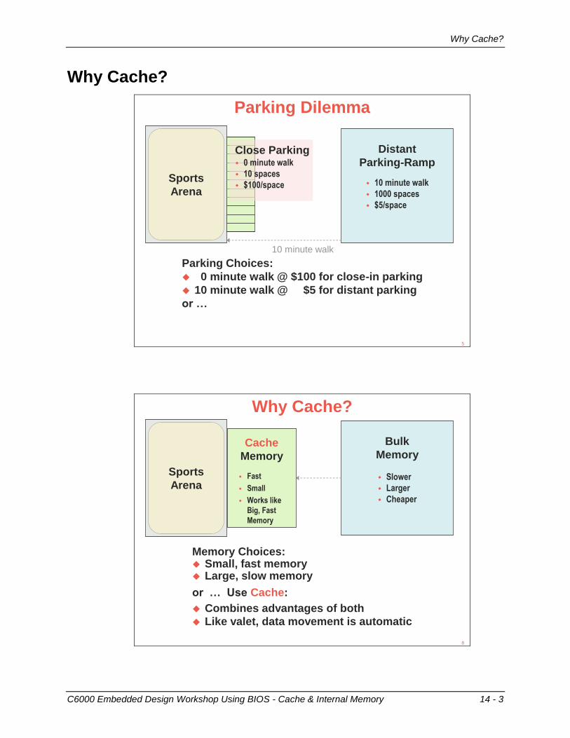
Why Cache?
C6000 Embedded Design Workshop Using BIOS - Cache & Internal Memory 14 - 3
Why Cache?
Parking Choices:
0 minute walk @ $100 for close-in parking
Parking Dilemma
Sports
Arena
Close Parking 0 minute walk
10 spaces
$100/space
Distant
Parking-Ramp
10 minute walk
10 minute walk
1000 spaces
$5/space
Parking Choices:
0 minute walk @ $100 for close-in parking
10 minute walk @ $5 for distant parking
Parking Choices:
0 minute walk @ $100 for close-in parking
10 minute walk @ $5 for distant parking
or …
5
Why Cache?
Sports
Arena
Bulk
MemoryCache
Memory
Slower
Larger
Cheaper
Memory Choices: Small, fast memory Large, slow memory
or … Use Cache:
Combines advantages of both
Like valet, data movement is automatic
Fast
Small
Works like
Big, Fast
Memory
8
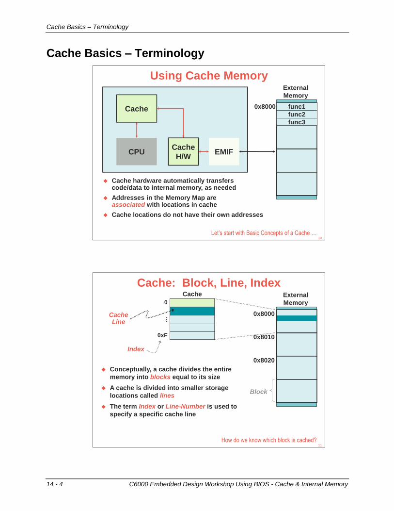
Cache Basics – Terminology
14 - 4 C6000 Embedded Design Workshop Using BIOS - Cache & Internal Memory
Cache Basics – Terminology
CPU
Cache
Cache
H/W
Using Cache MemoryExternal
Memory
EMIF
Programfunc1
func2
func3
0x8000
Cache hardware automatically transfers code/data to internal memory, as needed
Addresses in the Memory Map are associated with locations in cache
Cache locations do not have their own addresses
Let’s start with Basic Concepts of a Cache …10
Cache: Block, Line, Index
0x8000
Conceptually, a cache divides the entire
memory into blocks equal to its size
A cache is divided into smaller storage
locations called lines
The term Index or Line-Number is used to
specify a specific cache line
0x8010
0x8020
Cache
0
...
0xF
Block
CacheLine
Index
How do we know which block is cached?
External
Memory
11
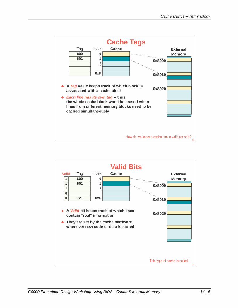
Cache Basics – Terminology
C6000 Embedded Design Workshop Using BIOS - Cache & Internal Memory 14 - 5
Cache Tags
0x8000
A Tag value keeps track of which block is
associated with a cache block
Each line has its own tag -- thus,
the whole cache block won’t be erased when
lines from different memory blocks need to be
cached simultaneously
0x8010
0x8020
Tag Index Cache
800 0
801 1...
0xF
How do we know a cache line is valid (or not)?
External
Memory
12
Valid Bits
0x8000
A Valid bit keeps track of which lines
contain “real” information
They are set by the cache hardware
whenever new code or data is stored
0x8010
0x8020
Tag Index Cache
800 0
801 1...
721 0xF
Valid
1
1...
0
0
This type of cache is called ...
External
Memory
13
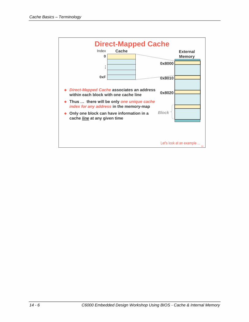
Cache Basics – Terminology
14 - 6 C6000 Embedded Design Workshop Using BIOS - Cache & Internal Memory
Direct-Mapped Cache
0x8000
0x8010
0x8020
Index Cache
0
...
0xF
Block
Direct-Mapped Cache associates an address
within each block with one cache line
Thus … there will be only one unique cache
index for any address in the memory-map
Only one block can have information in a
cache line at any given time
Let's look at an example ...
External
Memory
14
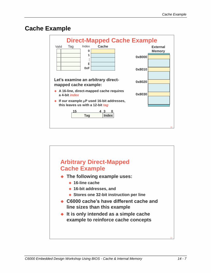
Cache Example
C6000 Embedded Design Workshop Using BIOS - Cache & Internal Memory 14 - 7
Cache Example
Direct-Mapped Cache Example
0x8000
0x8010
0x8020
0x8030
IndexTag
3 015 4
Tag Index Cache
0
1...
E
0xF
Let’s examine an arbitrary direct-
mapped cache example:
A 16-line, direct-mapped cache requires
a 4-bit index
If our example P used 16-bit addresses,
this leaves us with a 12-bit tag
Valid External
Memory
16
Arbitrary Direct-Mapped Cache Example
The following example uses:
16-line cache
16-bit addresses, and
Stores one 32-bit instruction per line
C6000 cache’s have different cache and
line sizes than this example
It is only intended as a simple cache
example to reinforce cache concepts
17
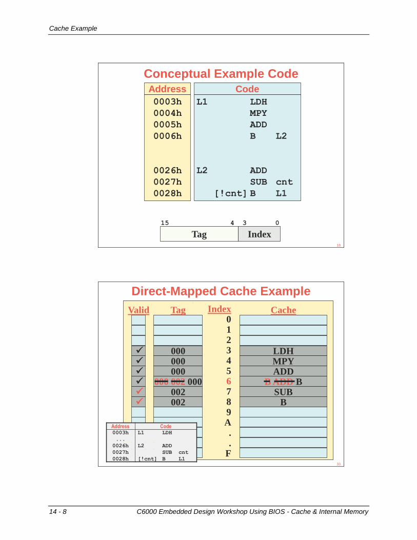
Cache Example
14 - 8 C6000 Embedded Design Workshop Using BIOS - Cache & Internal Memory
Conceptual Example Code
0003h
0004h
0005h
0006h
0026h
0027h
0028h
L1 LDH
MPY
ADD
B L2
L2 ADD
SUB cnt
[!cnt] B L1
CodeAddress
Tag Index
15 4 3 0
18
Direct-Mapped Cache Example
Index0123456789A..
F
LDHMPYADD
B ADD BSUB
B
Cache
000000000
000 002 000002002
Tag
Valid
Address Code0003h L1 LDH
...
0026h L2 ADD
0027h SUB cnt
0028h [!cnt] B L133
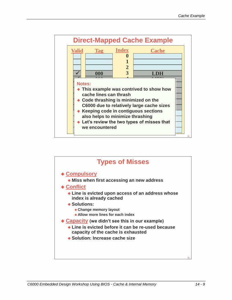
Cache Example
C6000 Embedded Design Workshop Using BIOS - Cache & Internal Memory 14 - 9
Direct-Mapped Cache Example
Index0123456789A..
F
LDHMPYADD
BADDSUB
B
Cache
000000000000002002002
Tag
Valid
Notes:
This example was contrived to show how
cache lines can thrash
Code thrashing is minimized on the
C6000 due to relatively large cache sizes
Keeping code in contiguous sections
also helps to minimize thrashing
Let’s review the two types of misses that
we encountered
34
Types of Misses
CompulsoryMiss when first accessing an new address
Conflict Line is evicted upon access of an address whose
index is already cached
Solutions: Change memory layout
Allow more lines for each index
Capacity (we didn’t see this in our example)
Line is evicted before it can be re-used because capacity of the cache is exhausted
Solution: Increase cache size
35
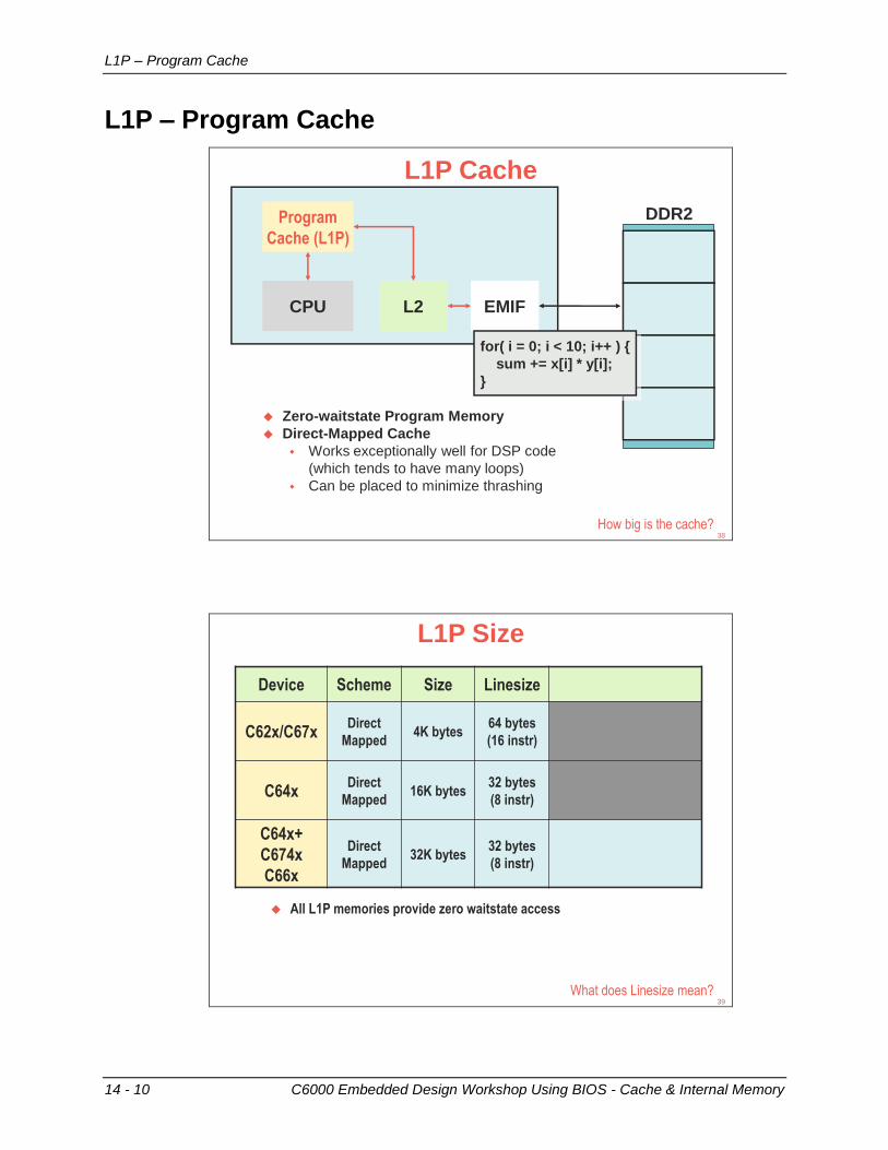
L1P – Program Cache
14 - 10 C6000 Embedded Design Workshop Using BIOS - Cache & Internal Memory
L1P – Program Cache
L1P Cache
DDR2
CPU
Program
Cache (L1P)
L2 EMIF
How big is the cache?
Zero-waitstate Program Memory
Direct-Mapped Cache
Works exceptionally well for DSP code
(which tends to have many loops)
Can be placed to minimize thrashing
for( i = 0; i < 10; i++ ) {
sum += x[i] * y[i];
}
38
L1P Size
Device Scheme Size Linesize
C62x/C67xDirect
Mapped4K bytes
64 bytes
(16 instr)
C64xDirect
Mapped16K bytes
32 bytes
(8 instr)
C64x+
C674x
C66x
Direct
Mapped32K bytes
32 bytes
(8 instr)
What does Linesize mean?
All L1P memories provide zero waitstate access
39
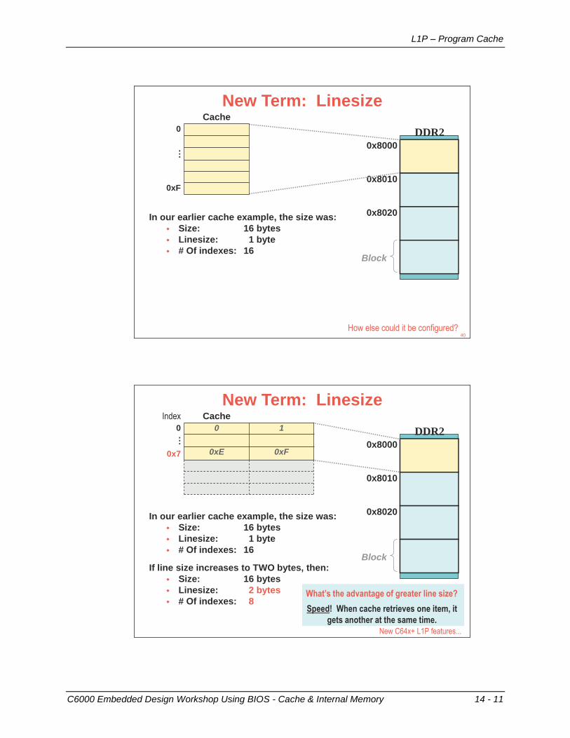
L1P – Program Cache
C6000 Embedded Design Workshop Using BIOS - Cache & Internal Memory 14 - 11
New Term: Linesize
0x8000
0x8010
0x8020
Block
Cache
0
...
0xF
In our earlier cache example, the size was:
Size: 16 bytes
Linesize: 1 byte
# Of indexes: 16
How else could it be configured?
DDR2
40
New Term: Linesize
0x8000
0x8010
0x8020
Block
Index Cache
0 0 1...
0x7 0xE 0xF
In our earlier cache example, the size was:
Size: 16 bytes
Linesize: 1 byte
# Of indexes: 16
If line size increases to TWO bytes, then:
Size: 16 bytes
Linesize: 2 bytes
# Of indexes: 8What’s the advantage of greater line size?
Speed! When cache retrieves one item, it
gets another at the same time.
New C64x+ L1P features...
DDR2

L1P – Program Cache
14 - 12 C6000 Embedded Design Workshop Using BIOS - Cache & Internal Memory
L1P Cache Comparison
Device Scheme Size Linesize New Features
C62x/C67xDirect
Mapped4K bytes
64 bytes
(16 instr)N/A
C64xDirect
Mapped16K bytes
32 bytes
(8 instr)N/A
C64x+C674xC66x
Direct
Mapped32K bytes
32 bytes
(8 instr)
Cache/RAM
Cache Freeze
Memory Protection
Next two slides discuss Cache/RAM and Freeze features.
Memory Protection is not discussed in this workshop.
All L1P memories provide zero waitstate access
Cache/Ram...42
C64x+ L1P – Cache vs. Addressable RAM32K
16K
8K
4K
Can be configured as Cache or
Addressable RAM
Five cache sizes are available:
0K, 4K, 8K, 16K, 32K
Allows critical loops to be put
into L1P, while still affording
room for cache memory
RAM Memory
Cache
Cache Freeze...43
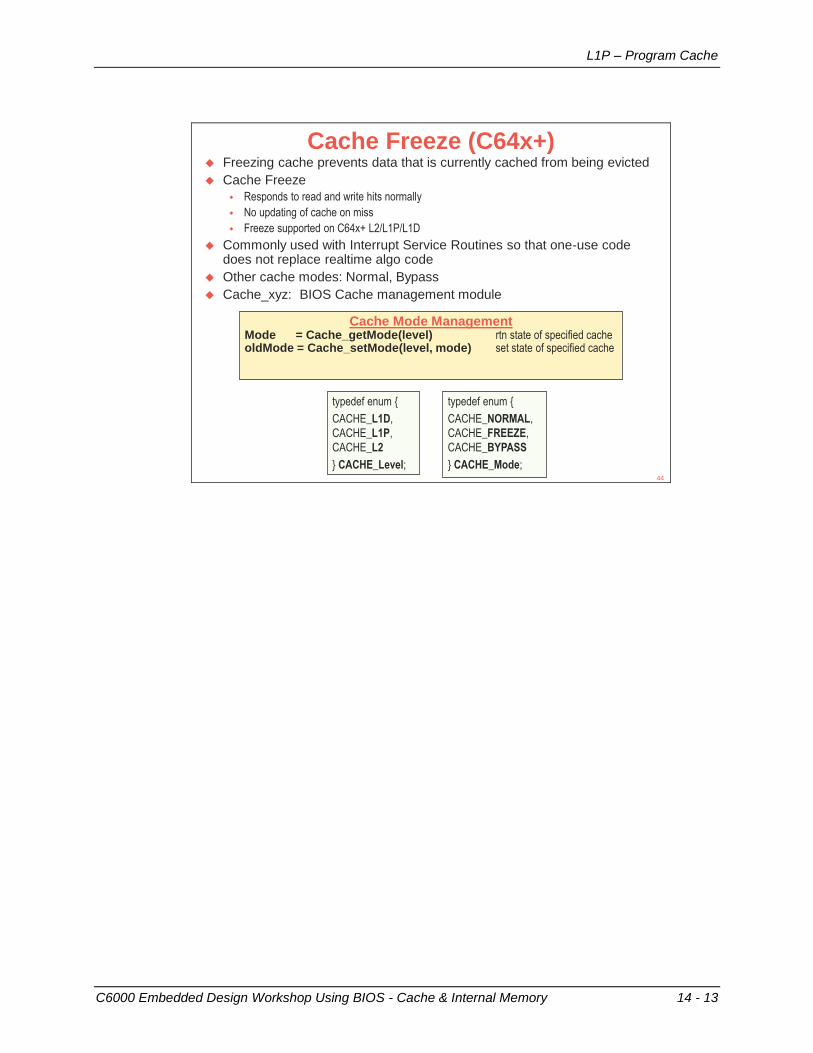
L1P – Program Cache
C6000 Embedded Design Workshop Using BIOS - Cache & Internal Memory 14 - 13
Cache Freeze (C64x+) Freezing cache prevents data that is currently cached from being evicted
Cache Freeze
Responds to read and write hits normally
No updating of cache on miss
Freeze supported on C64x+ L2/L1P/L1D
Commonly used with Interrupt Service Routines so that one-use code does not replace realtime algo code
Other cache modes: Normal, Bypass
Cache_xyz: BIOS Cache management module
Cache Mode ManagementMode = Cache_getMode(level) rtn state of specified cacheoldMode = Cache_setMode(level, mode) set state of specified cache
typedef enum {
CACHE_NORMAL,
CACHE_FREEZE,
CACHE_BYPASS
} CACHE_Mode;
typedef enum {
CACHE_L1D,
CACHE_L1P,
CACHE_L2
} CACHE_Level;44
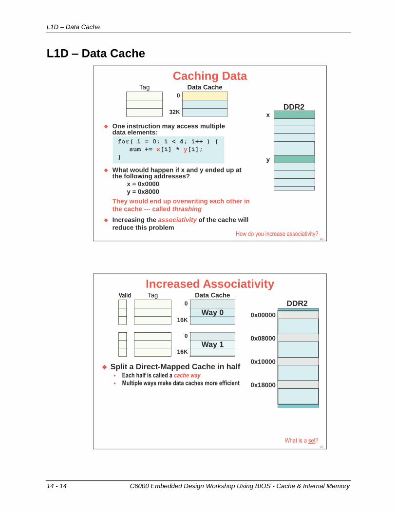
L1D – Data Cache
14 - 14 C6000 Embedded Design Workshop Using BIOS - Cache & Internal Memory
L1D – Data Cache
Caching Data
for( i = 0; i < 4; i++ ) {
sum += x[i] * y[i];
}
One instruction may access multiple data elements:
Tag Data Cache
0
32K
What would happen if x and y ended up at the following addresses?
x = 0x0000
y = 0x8000
DDR2x
y
They would end up overwriting each other in
the cache --- called thrashing
Increasing the associativity of the cache will
reduce this problemHow do you increase associativity?
46
Increased Associativity
DDR2
0x00000
0x08000
0x10000
0x18000
Valid Tag Data Cache
0
16K
0
16K
Way 0
Way 1
Split a Direct-Mapped Cache in half Each half is called a cache way
Multiple ways make data caches more efficient
What is a set?47
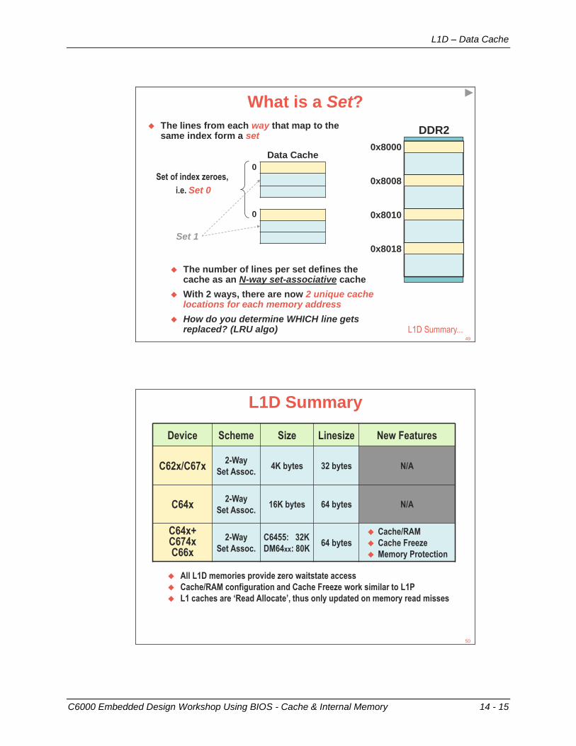
L1D – Data Cache
C6000 Embedded Design Workshop Using BIOS - Cache & Internal Memory 14 - 15
What is a Set?
0x8000
The lines from each way that map to the same index form a set
0x8008
0x8010
0x8018
Data Cache
0
0
Set of index zeroes,
i.e. Set 0
The number of lines per set defines the cache as an N-way set-associative cache
With 2 ways, there are now 2 unique cache locations for each memory address
How do you determine WHICH line gets replaced? (LRU algo)
Set 1
L1D Summary...
DDR2
49
L1D Summary
Device Scheme Size Linesize New Features
C62x/C67x2-Way
Set Assoc.4K bytes 32 bytes N/A
C64x2-Way
Set Assoc.16K bytes 64 bytes N/A
C64x+C674xC66x
2-Way
Set Assoc.
C6455: 32K
DM64xx: 80K64 bytes
Cache/RAM
Cache Freeze
Memory Protection
All L1D memories provide zero waitstate access
Cache/RAM configuration and Cache Freeze work similar to L1P
L1 caches are ‘Read Allocate’, thus only updated on memory read misses
50
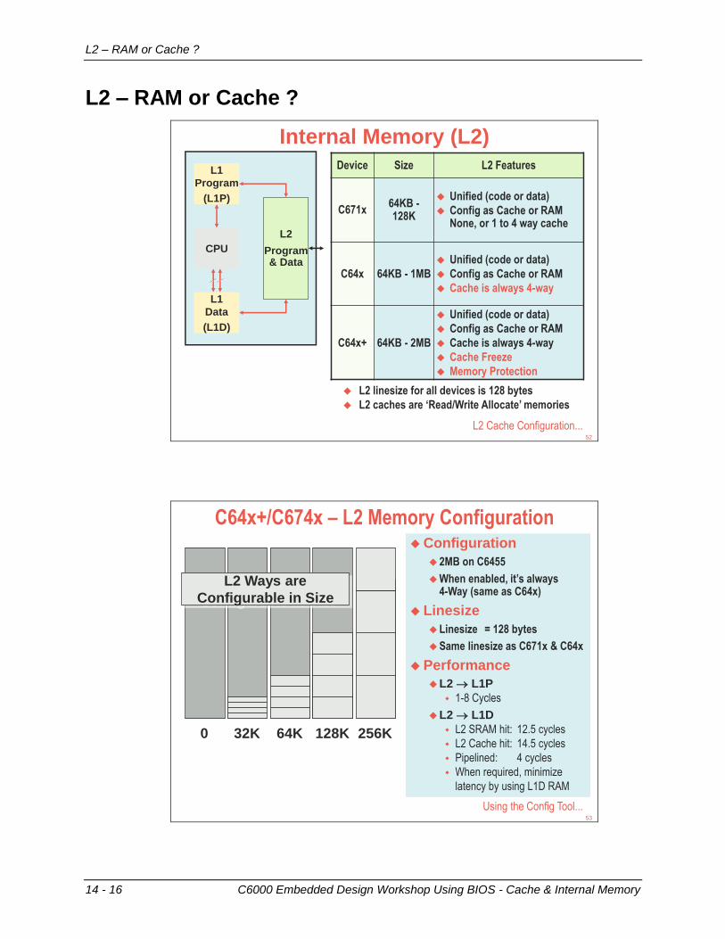
L2 – RAM or Cache ?
14 - 16 C6000 Embedded Design Workshop Using BIOS - Cache & Internal Memory
L2 – RAM or Cache ?
Internal Memory (L2)
CPU
L1
Program
(L1P)
L1
Data
(L1D)
L2
Program& Data
Device Size L2 Features
C671x64KB -128K
Unified (code or data)
Config as Cache or RAMNone, or 1 to 4 way cache
C64x 64KB - 1MB
Unified (code or data)
Config as Cache or RAM
Cache is always 4-way
C64x+ 64KB - 2MB
Unified (code or data)
Config as Cache or RAM
Cache is always 4-way
Cache Freeze
Memory Protection
L2 linesize for all devices is 128 bytes
L2 caches are ‘Read/Write Allocate’ memories
L2 Cache Configuration...52
C64x+/C674x – L2 Memory ConfigurationConfiguration
2MB on C6455
When enabled, it’s always 4-Way (same as C64x)
Linesize
Linesize = 128 bytes
Same linesize as C671x & C64x
Performance
L2 L1P
1-8 Cycles
L2 L1D
L2 SRAM hit: 12.5 cycles
L2 Cache hit: 14.5 cycles
Pipelined: 4 cycles
When required, minimize
latency by using L1D RAM
L2 Ways are
Configurable in Size
0 32K 64K 128K 256K
Using the Config Tool...53
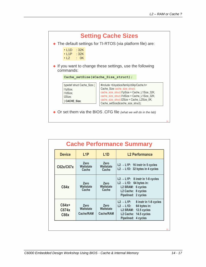
L2 – RAM or Cache ?
C6000 Embedded Design Workshop Using BIOS - Cache & Internal Memory 14 - 17
Setting Cache Sizes
The default settings for TI-RTOS (via platform file) are:
• L1D : 32K
• L1P : 32K
• L2 : 0K
54
If you want to change these settings, use the following commands:
Cache_setSize(&Cache_Size_struct);
#include <ti/sysbios/family/c64p/Cache.h>
Cache_Size cache_size_struct;
cache_size_struct.l1pSize = Cache_L1Size_32K;
cache_size_struct.l1dSize = Cache_L1Size_32K;
cache_size_struct.l2Size = Cache_L2Size_0K;
Cache_setSize(&cache_size_struct);
typedef struct Cache_Size {
l1pSize;
l1dSize;
l2Size;
} CACHE_Size;
Or set them via the BIOS .CFG file (what we will do in the lab)
Cache Performance Summary
Device L1P L1D L2 Performance
C62x/C67xZero
WaitstateCache
Zero Waitstate
Cache
L2 → L1P: 16 instr in 5 cycles
L2 → L1D: 32 bytes in 4 cycles
C64xZero
WaitstateCache
Zero Waitstate
Cache
L2 → L1P: 8 instr in 1-8 cycles
L2 → L1D: 64 bytes in:
L2 SRAM: 6 cycles
L2 Cache: 8 cycles
Pipelined: 2 cycles
C64x+
C674x
C66x
Zero Waitstate
Cache/RAM
Zero Waitstate
Cache/RAM
L2 → L1P: 8 instr in 1-8 cycles
L2 → L1D: 64 bytes in:
L2 SRAM: 12.5 cycles
L2 Cache: 14.5 cycles
Pipelined: 4 cycles
55
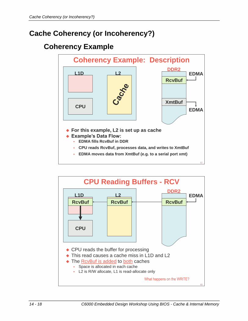
Cache Coherency (or Incoherency?)
14 - 18 C6000 Embedded Design Workshop Using BIOS - Cache & Internal Memory
Cache Coherency (or Incoherency?)
Coherency Example
Coherency Example: Description
CPU
L2DDR2
L1D
For this example, L2 is set up as cache
Example’s Data Flow: EDMA fills RcvBuf in DDR
CPU reads RcvBuf, processes data, and writes to XmtBuf
EDMA moves data from XmtBuf (e.g. to a serial port xmt)
RcvBuf
XmtBuf
EDMA
EDMA
57
CPU Reading Buffers - RCV
CPU
L2L1D
RcvBufRcvBuf RcvBuf
EDMA
CPU reads the buffer for processing
This read causes a cache miss in L1D and L2
The RcvBuf is added to both caches Space is allocated in each cache
L2 is R/W allocate, L1 is read-allocate only
DDR2
What happens on the WRITE?
60
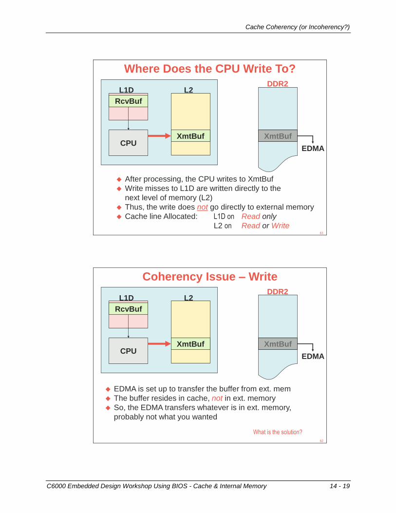
Cache Coherency (or Incoherency?)
C6000 Embedded Design Workshop Using BIOS - Cache & Internal Memory 14 - 19
Where Does the CPU Write To?
CPU
L2L1D
RcvBuf
XmtBuf
After processing, the CPU writes to XmtBuf
Write misses to L1D are written directly to the
next level of memory (L2)
Thus, the write does not go directly to external memory
Cache line Allocated: L1D on Read only
L2 on Read or Write
XmtBuf
EDMA
DDR2
61
Coherency Issue – Write
CPU
L2L1D
XmtBuf
RcvBuf
EDMA
EDMA is set up to transfer the buffer from ext. mem
The buffer resides in cache, not in ext. memory
So, the EDMA transfers whatever is in ext. memory,
probably not what you wanted
What is the solution?
XmtBuf
DDR2
62
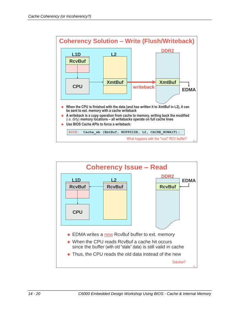
Cache Coherency (or Incoherency?)
14 - 20 C6000 Embedded Design Workshop Using BIOS - Cache & Internal Memory
Coherency Solution – Write (Flush/Writeback)
CPU
L2L1D
XmtBuf
RcvBuf
XmtBuf
EDMA
When the CPU is finished with the data (and has written it to XmtBuf in L2), it can be sent to ext. memory with a cache writeback
A writeback is a copy operation from cache to memory, writing back the modified (i.e. dirty) memory locations – all writebacks operate on full cache lines
Use BIOS Cache APIs to force a writeback:
writeback
BIOS: Cache_wb (XmtBuf, BUFFSIZE, L2, CACHE_NOWAIT);
DDR2
What happens with the "next" RCV buffer?63
Coherency Issue – Read
CPU
L2L1D
RcvBufRcvBuf RcvBuf
EDMA
EDMA writes a new RcvBuf buffer to ext. memory
When the CPU reads RcvBuf a cache hit occurs since the buffer (with old “stale” data) is still valid in cache
Thus, the CPU reads the old data instead of the new
DDR2
Solution?64
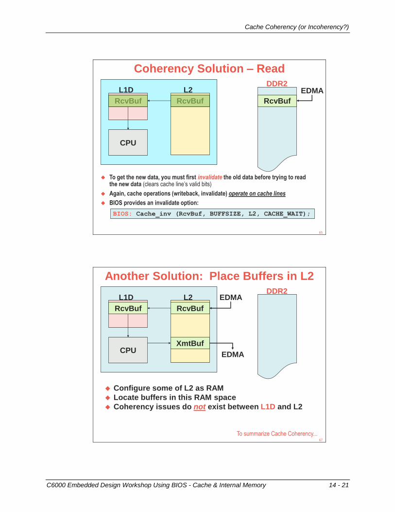
Cache Coherency (or Incoherency?)
C6000 Embedded Design Workshop Using BIOS - Cache & Internal Memory 14 - 21
Coherency Solution – Read
CPU
L2L1D
RcvBufRcvBuf RcvBuf
EDMA
To get the new data, you must first invalidate the old data before trying to read the new data (clears cache line’s valid bits)
Again, cache operations (writeback, invalidate) operate on cache lines
BIOS provides an invalidate option:
BIOS: Cache_inv (RcvBuf, BUFFSIZE, L2, CACHE_WAIT);
DDR2
65
Another Solution: Place Buffers in L2
CPU
L2L1D
RcvBuf RcvBuf
XmtBuf
EDMA
Configure some of L2 as RAM
Locate buffers in this RAM space
Coherency issues do not exist between L1D and L2
EDMA
To summarize Cache Coherency...
DDR2
67
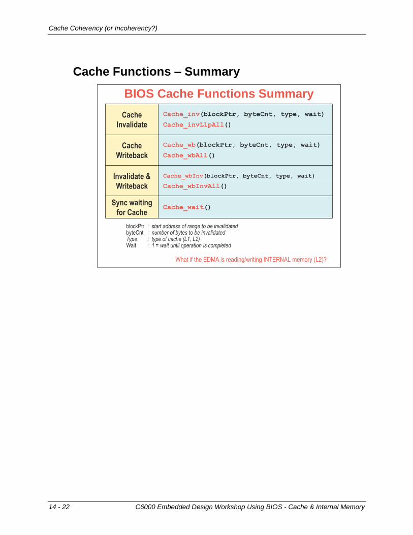
Cache Coherency (or Incoherency?)
14 - 22 C6000 Embedded Design Workshop Using BIOS - Cache & Internal Memory
Cache Functions – Summary
BIOS Cache Functions Summary
blockPtr : start address of range to be invalidatedbyteCnt : number of bytes to be invalidatedType : type of cache (L1, L2)Wait : 1 = wait until operation is completed
Cache
Invalidate
Cache_inv(blockPtr, byteCnt, type, wait)
Cache_invL1pAll()
Cache
Writeback
Cache_wb(blockPtr, byteCnt, type, wait)
Cache_wbAll()
Invalidate &
Writeback
Cache_wbInv(blockPtr, byteCnt, type, wait)
Cache_wbInvAll()
Sync waiting
for CacheCache_wait()
What if the EDMA is reading/writing INTERNAL memory (L2)?
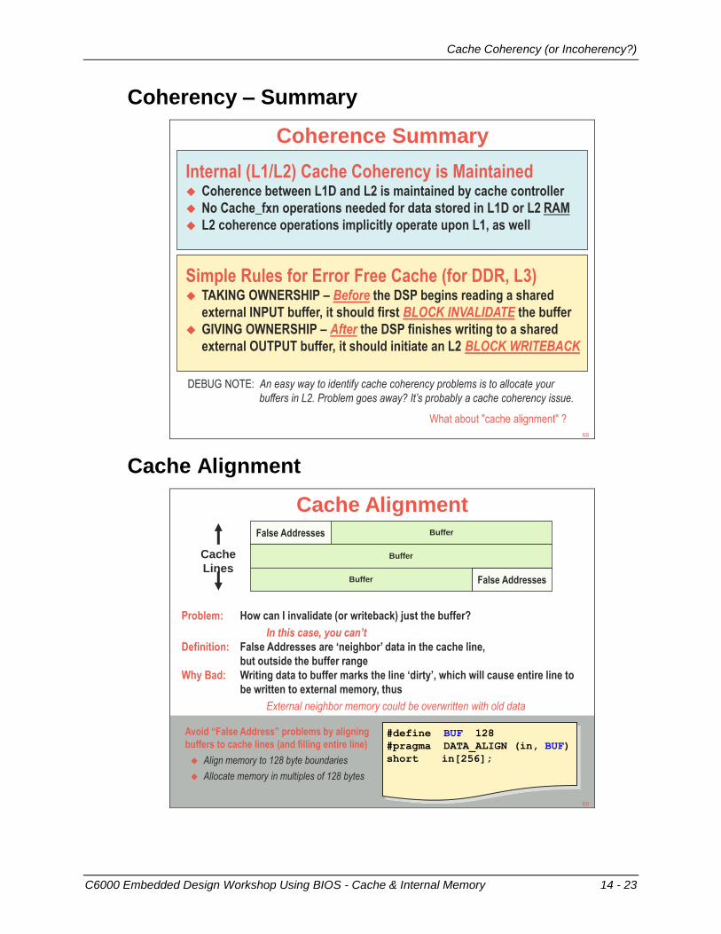
Cache Coherency (or Incoherency?)
C6000 Embedded Design Workshop Using BIOS - Cache & Internal Memory 14 - 23
Coherency – Summary
Coherence Summary
Internal (L1/L2) Cache Coherency is Maintained Coherence between L1D and L2 is maintained by cache controller
No Cache_fxn operations needed for data stored in L1D or L2 RAM
L2 coherence operations implicitly operate upon L1, as well
Simple Rules for Error Free Cache (for DDR, L3) TAKING OWNERSHIP – Before the DSP begins reading a shared
external INPUT buffer, it should first BLOCK INVALIDATE the buffer
GIVING OWNERSHIP – After the DSP finishes writing to a shared
external OUTPUT buffer, it should initiate an L2 BLOCK WRITEBACK
What about "cache alignment" ?
DEBUG NOTE: An easy way to identify cache coherency problems is to allocate your
buffers in L2. Problem goes away? It’s probably a cache coherency issue.
68
Cache Alignment
False Addresses
False Addresses Buffer
Buffer
Buffer
Cache
Lines
Problem: How can I invalidate (or writeback) just the buffer?
In this case, you can’t
Definition: False Addresses are ‘neighbor’ data in the cache line,
but outside the buffer range
Why Bad: Writing data to buffer marks the line ‘dirty’, which will cause entire line to
be written to external memory, thus
External neighbor memory could be overwritten with old data
Cache Alignment
Avoid “False Address” problems by aligning
buffers to cache lines (and filling entire line)
Align memory to 128 byte boundaries
Allocate memory in multiples of 128 bytes
#define BUF 128
#pragma DATA_ALIGN (in, BUF)
short in[256];
69
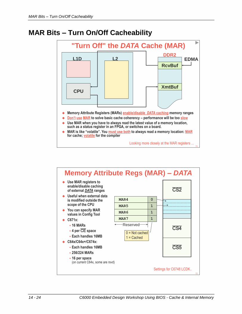
MAR Bits – Turn On/Off Cacheability
14 - 24 C6000 Embedded Design Workshop Using BIOS - Cache & Internal Memory
MAR Bits – Turn On/Off Cacheability
"Turn Off" the DATA Cache (MAR)
CPU
L2L1D
RcvBuf
XmtBuf
EDMA
Memory Attribute Registers (MARs) enable/disable DATA caching memory ranges
Don’t use MAR to solve basic cache coherency – performance will be too slow
Use MAR when you have to always read the latest value of a memory location, such as a status register in an FPGA, or switches on a board.
MAR is like “volatile”. You must use both to always read a memory location: MARfor cache; volatile for the compiler
Looking more closely at the MAR registers ...
DDR2
71
Memory Attribute Regs (MAR) – DATA
CS2
CS4
CS5
0 = Not cached
1 = Cached
MAR4 0
MAR5 1
MAR6 1
MAR7 1
Reserved
Use MAR registers to enable/disable caching of external DATA ranges
Useful when external data is modified outside the scope of the CPU
You can specify MAR values in Config Tool
C671x:
16 MARs
4 per CE space
Each handles 16MB
C64x/C64x+/C674x:
Each handles 16MB
256/224 MARs
16 per space(on current C64x, some are rsvd)
Settings for C6748 LCDK..72
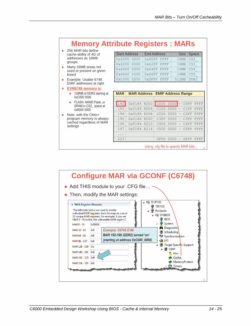
MAR Bits – Turn On/Off Cacheability
C6000 Embedded Design Workshop Using BIOS - Cache & Internal Memory 14 - 25
Memory Attribute Registers : MARs
Start Address End Address Size Space
0x6000 0000 0x60FF FFFF 16MB CS2_
0x6200 0000 0x62FF FFFF 16MB CS3_
0x6400 0000 0x64FF FFFF 16MB CS4_
0x6600 0000 0x66FF FFFF 16MB CS5_
0xC000 0000 0xDFFF FFFF 512MB DDR2
MAR MAR Address EMIF Address Range
192 0x0184 8200 C000 0000 – C0FF FFFF
193 0x0184 8204 C100 0000 – C1FF FFFF
194 0x0184 8208 C200 0000 – C2FF FFFF
195 0x0184 820C C300 0000 – C3FF FFFF
196 0x0184 8210 C400 0000 – C4FF FFFF
197 0x0184 8214 C500 0000 – C5FF FFFF
...
223 DF00 0000 – DFFF FFFF
256 MAR bits define cache-ability of 4G of addresses as 16MB groups
Many 16MB areas not used or present on given board
Example: Usable 6748 EMIF addresses at right
EVM6748 memory is:
128MB of DDR2 starting at 0xC000 0000
FLASH, NAND Flash, or SRAM in CS2_ space at 0x6000 0000
Note: with the C64x+ program memory is always cached regardless of MAR settings
73Using .cfg file to specify MAR bits…
Configure MAR via GCONF (C6748)
Then, modify the MAR settings:
74
Add THIS module to your .CFG file…
Example: C6748 EVM
MAR 192-199 (DDR2) turned ‘on’
(starting at address 0xC000_0000)
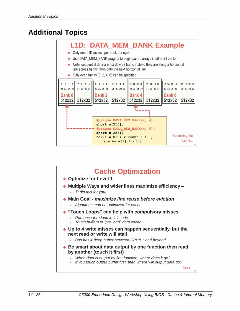
Additional Topics
14 - 26 C6000 Embedded Design Workshop Using BIOS - Cache & Internal Memory
Additional Topics
L1D: DATA_MEM_BANK Example Only one L1D access per bank per cycle
Use DATA_MEM_BANK pragma to begin paired arrays in different banks
Note: sequential data are not down a bank, instead they are along a horizontal
line across banks, then onto the next horizontal line
Only even banks (0, 2, 4, 6) can be specified
512x32
0123
20212223
512x32
4567
24252627
512x32
89AB
28292A2B
512x32
CDEF
2C2D2E2F
512x32
10111213
30313233
512x32
14151617
34353637
512x32
18191A1B
38393A3B
512x32
1C1D1E1F
3C3D3E3F
Bank 0 Bank 2 Bank 4 Bank 6
#pragma DATA_MEM_BANK(a, 4);
short a[256];
#pragma DATA_MEM_BANK(x, 0);
short x[256];
for(i = 0; i < count ; i++)
sum += a[i] * x[i];
Optimizing the
cache...76
Cache Optimization Optimize for Level 1
Multiple Ways and wider lines maximize efficiency –
TI did this for you!
Main Goal - maximize line reuse before eviction
Algorithms can be optimized for cache
“Touch Loops” can help with compulsory misses
Run once thru loop in init code Touch buffers to “pre-load” data cache
Up to 4 write misses can happen sequentially, but the next read or write will stall
Bus has 4 deep buffer between CPU/L1 and beyond
Be smart about data output by one function then read by another (touch it first)
When data is output by first function, where does it go? If you touch output buffer first, then where will output data go?
Docs...77
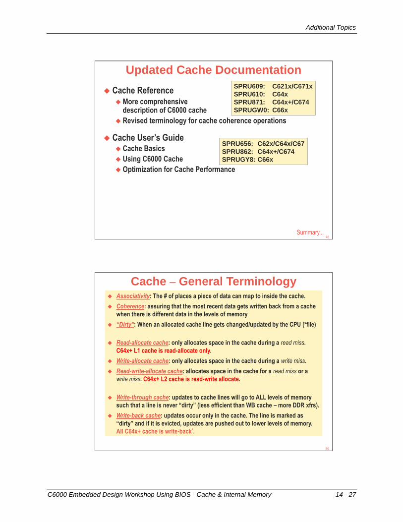
Additional Topics
C6000 Embedded Design Workshop Using BIOS - Cache & Internal Memory 14 - 27
Updated Cache Documentation
Cache Reference More comprehensive
description of C6000 cache
Revised terminology for cache coherence operations
Cache User’s Guide Cache Basics
Using C6000 Cache
Optimization for Cache Performance
SPRU656: C62x/C64x/C67
SPRU862: C64x+/C674
SPRUGY8: C66x
SPRU609: C621x/C671x
SPRU610: C64x
SPRU871: C64x+/C674
SPRUGW0: C66x
Summary...78
Cache – General Terminology Associativity: The # of places a piece of data can map to inside the cache.
Coherence: assuring that the most recent data gets written back from a cache
when there is different data in the levels of memory
“Dirty”: When an allocated cache line gets changed/updated by the CPU (*file)
Read-allocate cache: only allocates space in the cache during a read miss.
C64x+ L1 cache is read-allocate only.
Write-allocate cache: only allocates space in the cache during a write miss.
Read-write-allocate cache: allocates space in the cache for a read miss or a
write miss. C64x+ L2 cache is read-write allocate.
Write-through cache: updates to cache lines will go to ALL levels of memory
such that a line is never “dirty” (less efficient than WB cache – more DDR xfrs).
Write-back cache: updates occur only in the cache. The line is marked as
“dirty” and if it is evicted, updates are pushed out to lower levels of memory.
All C64x+ cache is write-back*.
80
Additional Topics
14 - 28 C6000 Embedded Design Workshop Using BIOS - Cache & Internal Memory
*** this page is not blank ***
Chapter Quiz
C6000 Embedded Design Workshop Using BIOS - Cache & Internal Memory 14 - 29
Chapter Quiz
Chapter Quiz1. How do you turn ON the cache ?
2. Name the three types of caches & their associated memories:
3. All cache operations affect an aligned cache line. How big is a line?
4. Which bit(s) turn on/off “cacheability” and where do you set these?
5. How do you fix coherency when two bus masters access ext’l mem?
6. If a dirty (newly written) cache line needs to be evicted, how does that dirty line get written out to external memory?
Chapter Quiz
14 - 30 C6000 Embedded Design Workshop Using BIOS - Cache & Internal Memory
Quiz – Answers
Chapter Quiz1. How do you turn ON the cache ?
2. Name the three types of caches & their associated memories:
3. All cache operations affect an aligned cache line. How big is a line?
4. Which bit(s) turn on/off “cacheability” and where do you set these?
5. How do you fix coherency when two bus masters access ext’l mem?
6. If a dirty (newly written) cache line needs to be evicted, how does that dirty line get written out to external memory?
• Set size > 0 in platform package (or via Cache_setSize() during runtime)
• Direct Mapped (L1P), 2-way (L1D), 4-way (L2)
• L1P – 32 bytes (256 bits), L1D – 64 bytes, L2 – 128 bytes
• Invalidate before a read, writeback after a write (or use L2 mem)
• MAR (Mem Attribute Register), affects 16MB Ext’l data space, .cfg
• Cache controller takes care of this
83
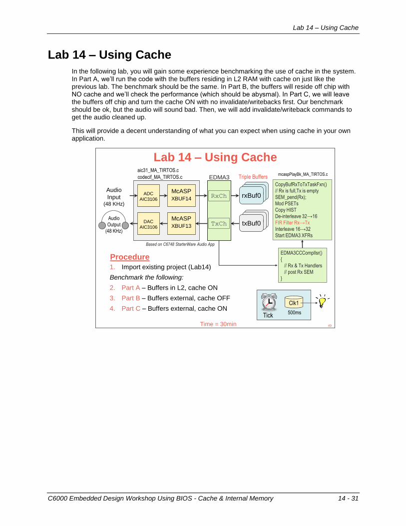
Lab 14 – Using Cache
C6000 Embedded Design Workshop Using BIOS - Cache & Internal Memory 14 - 31
Lab 14 – Using Cache
In the following lab, you will gain some experience benchmarking the use of cache in the system. In Part A, we’ll run the code with the buffers residing in L2 RAM with cache on just like the previous lab. The benchmark should be the same. In Part B, the buffers will reside off chip with NO cache and we’ll check the performance (which should be abysmal). In Part C, we will leave the buffers off chip and turn the cache ON with no invalidate/writebacks first. Our benchmark should be ok, but the audio will sound bad. Then, we will add invalidate/writeback commands to get the audio cleaned up.
This will provide a decent understanding of what you can expect when using cache in your own application.
Audio
Output
(48 KHz)
Lab 14 – Using Cache
ADC
AIC3106
Audio
Input (48 KHz)
McASP
XBUF14
DAC
AIC3106
McASP
XBUF13
1. Import existing project (Lab14)
Benchmark the following:
2. Part A – Buffers in L2, cache ON
3. Part B – Buffers external, cache OFF
4. Part C – Buffers external, cache ON
aic31_MA_TIRTOS.c
codecif_MA_TIRTOS.cmcaspPlayBk_MA_TIRTOS.c
rxBuf0rxBuf0rxBuf0
Triple Buffers
Time = 30min
Procedure
49
txBuf0txBuf0txBuf0
EDMA3
RxCh
TxCh
CopyBufRxToTxTaskFxn()
// Rx is full,Tx is empty
SEM_pend(Rx);
Mod PSETs
Copy HIST
De-interleave 32→16
FIR Filter Rx→Tx
Interleave 16→32
Start EDMA3 XFRs
EDMA3CCComplIsr()
{
// Rx & Tx Handlers
// post Rx SEM
}
Based on C6748 StarterWare Audio App
Clk1
Tick500ms
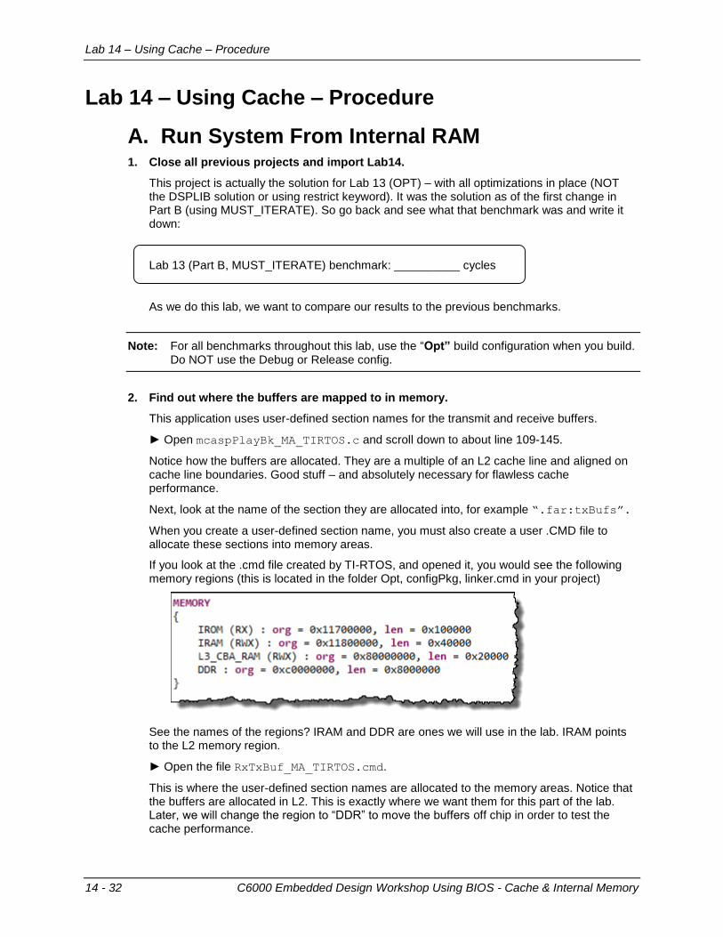
Lab 14 – Using Cache – Procedure
14 - 32 C6000 Embedded Design Workshop Using BIOS - Cache & Internal Memory
Lab 14 – Using Cache – Procedure
A. Run System From Internal RAM 1. Close all previous projects and import Lab14.
This project is actually the solution for Lab 13 (OPT) – with all optimizations in place (NOT the DSPLIB solution or using restrict keyword). It was the solution as of the first change in Part B (using MUST_ITERATE). So go back and see what that benchmark was and write it down:
Lab 13 (Part B, MUST_ITERATE) benchmark: __________ cycles
As we do this lab, we want to compare our results to the previous benchmarks.
Note: For all benchmarks throughout this lab, use the “Opt” build configuration when you build. Do NOT use the Debug or Release config.
2. Find out where the buffers are mapped to in memory.
This application uses user-defined section names for the transmit and receive buffers.
► Open mcaspPlayBk_MA_TIRTOS.c and scroll down to about line 109-145.
Notice how the buffers are allocated. They are a multiple of an L2 cache line and aligned on cache line boundaries. Good stuff – and absolutely necessary for flawless cache performance.
Next, look at the name of the section they are allocated into, for example “.far:txBufs”.
When you create a user-defined section name, you must also create a user .CMD file to allocate these sections into memory areas.
If you look at the .cmd file created by TI-RTOS, and opened it, you would see the following memory regions (this is located in the folder Opt, configPkg, linker.cmd in your project)
See the names of the regions? IRAM and DDR are ones we will use in the lab. IRAM points to the L2 memory region.
► Open the file RxTxBuf_MA_TIRTOS.cmd.
This is where the user-defined section names are allocated to the memory areas. Notice that the buffers are allocated in L2. This is exactly where we want them for this part of the lab. Later, we will change the region to “DDR” to move the buffers off chip in order to test the cache performance.
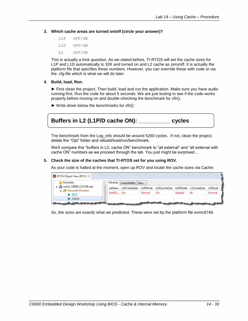
Lab 14 – Using Cache – Procedure
C6000 Embedded Design Workshop Using BIOS - Cache & Internal Memory 14 - 33
3. Which cache areas are turned on/off (circle your answer)?
L1P OFF/ON
L1D OFF/ON
L2 OFF/ON
This is actually a trick question. As we stated before, TI-RTOS will set the cache sizes for L1P and L1D automatically to 32K and turned on and L2 cache as zero/off. It is actually the platform file that specifies these numbers. However, you can override these with code or via the .cfg file which is what we will do later.
4. Build, load, Run.
► First clean the project. Then build, load and run the application. Make sure you have audio running first. Run the code for about 5 seconds. We are just testing to see if the code works properly before moving on and double-checking the benchmark for cfir().
► Write down below the benchmarks for cfir():
Buffers in L2 (L1P/D cache ON): __________ cycles
The benchmark from the Log_info should be around 5260 cycles. If not, clean the project, delete the “Opt” folder and rebuild/load/run/benchmark.
We’ll compare this “buffers in L2, cache ON” benchmark to “all external” and “all external with cache ON” numbers as we proceed through the lab. You just might be surprised…
5. Check the size of the caches that TI-RTOS set for you using ROV.
As your code is halted at the moment, open up ROV and locate the cache sizes via Cache:
So, the sizes are exactly what we predicted. These were set by the platform file evmc6748.
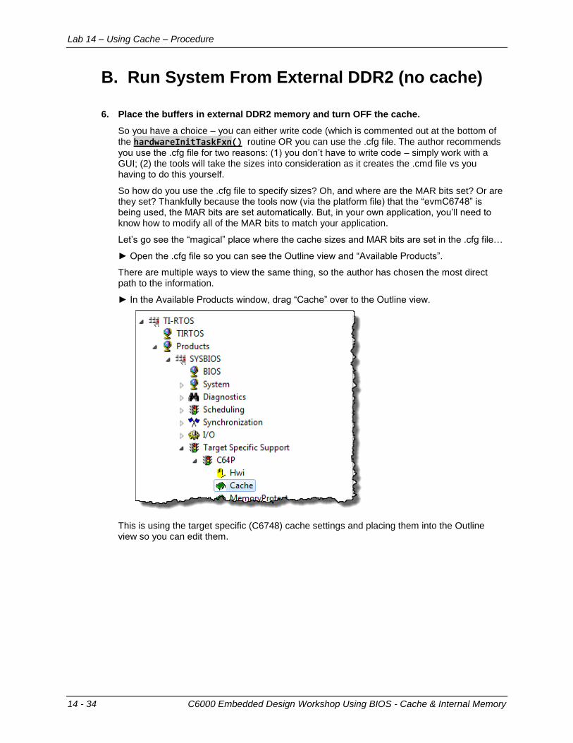
Lab 14 – Using Cache – Procedure
14 - 34 C6000 Embedded Design Workshop Using BIOS - Cache & Internal Memory
B. Run System From External DDR2 (no cache)
6. Place the buffers in external DDR2 memory and turn OFF the cache.
So you have a choice – you can either write code (which is commented out at the bottom of the hardwareInitTaskFxn() routine OR you can use the .cfg file. The author recommends
you use the .cfg file for two reasons: (1) you don’t have to write code – simply work with a GUI; (2) the tools will take the sizes into consideration as it creates the .cmd file vs you having to do this yourself.
So how do you use the .cfg file to specify sizes? Oh, and where are the MAR bits set? Or are they set? Thankfully because the tools now (via the platform file) that the “evmC6748” is being used, the MAR bits are set automatically. But, in your own application, you’ll need to know how to modify all of the MAR bits to match your application.
Let’s go see the “magical” place where the cache sizes and MAR bits are set in the .cfg file…
► Open the .cfg file so you can see the Outline view and “Available Products”.
There are multiple ways to view the same thing, so the author has chosen the most direct path to the information.
► In the Available Products window, drag “Cache” over to the Outline view.
This is using the target specific (C6748) cache settings and placing them into the Outline view so you can edit them.
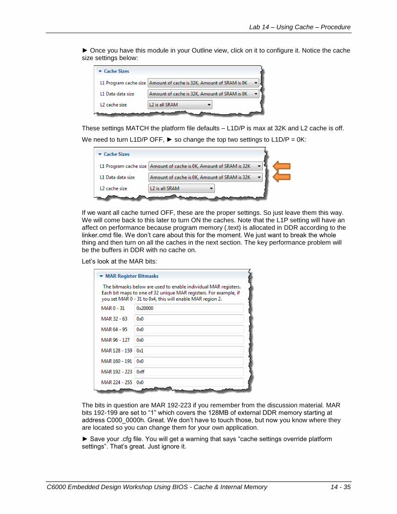
Lab 14 – Using Cache – Procedure
C6000 Embedded Design Workshop Using BIOS - Cache & Internal Memory 14 - 35
► Once you have this module in your Outline view, click on it to configure it. Notice the cache size settings below:
These settings MATCH the platform file defaults – L1D/P is max at 32K and L2 cache is off.
We need to turn L1D/P OFF, ► so change the top two settings to L1D/P = 0K:
If we want all cache turned OFF, these are the proper settings. So just leave them this way. We will come back to this later to turn ON the caches. Note that the L1P setting will have an affect on performance because program memory (.text) is allocated in DDR according to the linker.cmd file. We don’t care about this for the moment. We just want to break the whole thing and then turn on all the caches in the next section. The key performance problem will be the buffers in DDR with no cache on.
Let’s look at the MAR bits:
The bits in question are MAR 192-223 if you remember from the discussion material. MAR bits 192-199 are set to “1” which covers the 128MB of external DDR memory starting at address C000_0000h. Great. We don’t have to touch those, but now you know where they are located so you can change them for your own application.
► Save your .cfg file. You will get a warning that says “cache settings override platform settings”. That’s great. Just ignore it.
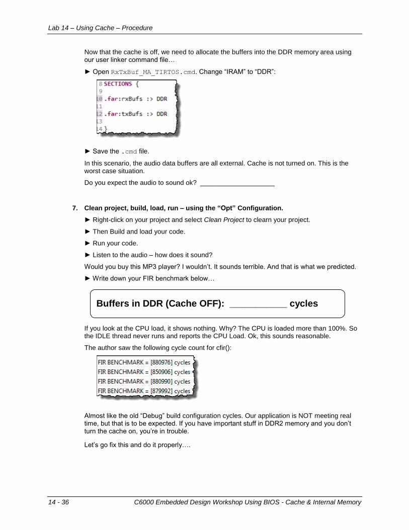
Lab 14 – Using Cache – Procedure
14 - 36 C6000 Embedded Design Workshop Using BIOS - Cache & Internal Memory
Now that the cache is off, we need to allocate the buffers into the DDR memory area using our user linker command file…
► Open RxTxBuf_MA_TIRTOS.cmd. Change “IRAM” to “DDR”:
► Save the .cmd file.
In this scenario, the audio data buffers are all external. Cache is not turned on. This is the worst case situation.
Do you expect the audio to sound ok? ____________________
7. Clean project, build, load, run – using the “Opt” Configuration.
► Right-click on your project and select Clean Project to clearn your project.
► Then Build and load your code.
► Run your code.
► Listen to the audio – how does it sound?
Would you buy this MP3 player? I wouldn’t. It sounds terrible. And that is what we predicted.
► Write down your FIR benchmark below…
Buffers in DDR (Cache OFF): ___________ cycles
If you look at the CPU load, it shows nothing. Why? The CPU is loaded more than 100%. So the IDLE thread never runs and reports the CPU Load. Ok, this sounds reasonable.
The author saw the following cycle count for cfir():
Almost like the old “Debug” build configuration cycles. Our application is NOT meeting real time, but that is to be expected. If you have important stuff in DDR2 memory and you don’t turn the cache on, you’re in trouble.
Let’s go fix this and do it properly….
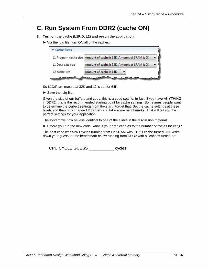
Lab 14 – Using Cache – Procedure
C6000 Embedded Design Workshop Using BIOS - Cache & Internal Memory 14 - 37
C. Run System From DDR2 (cache ON)
8. Turn on the cache (L1P/D, L2) and re-run the application.
► Via the .cfg file, turn ON all of the caches:
So L1D/P are maxed at 32K and L2 is set for 64K.
► Save the .cfg file.
Given the size of our buffers and code, this is a good setting. In fact, if you have ANYTHING in DDR2, this is the recommended starting point for cache settings. Sometimes people want to determine the perfect settings from the start. Forget that. Set the cache settings at these levels and then only change L2 (larger) and take some benchmarks. That will tell you the perfect settings for your application.
The system we now have is identical to one of the slides in the discussion material.
► Before you run the new code, what is your prediction as to the number of cycles for cfir()?
The best case was 5260 cycles running from L2 SRAM with L1P/D cache turned ON. Write down your guess for the benchmark below running from DDR2 with all caches turned on:
CPU CYCLE GUESS ___________ cycles
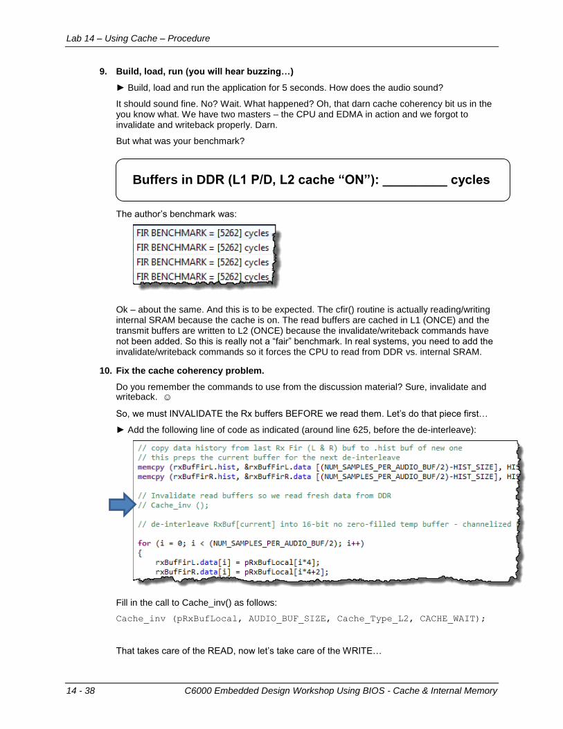
Lab 14 – Using Cache – Procedure
14 - 38 C6000 Embedded Design Workshop Using BIOS - Cache & Internal Memory
9. Build, load, run (you will hear buzzing…)
► Build, load and run the application for 5 seconds. How does the audio sound?
It should sound fine. No? Wait. What happened? Oh, that darn cache coherency bit us in the you know what. We have two masters – the CPU and EDMA in action and we forgot to invalidate and writeback properly. Darn.
But what was your benchmark?
Buffers in DDR (L1 P/D, L2 cache “ON”): _________ cycles
The author’s benchmark was:
Ok – about the same. And this is to be expected. The cfir() routine is actually reading/writing internal SRAM because the cache is on. The read buffers are cached in L1 (ONCE) and the transmit buffers are written to L2 (ONCE) because the invalidate/writeback commands have not been added. So this is really not a “fair” benchmark. In real systems, you need to add the invalidate/writeback commands so it forces the CPU to read from DDR vs. internal SRAM.
10. Fix the cache coherency problem.
Do you remember the commands to use from the discussion material? Sure, invalidate and writeback. ☺
So, we must INVALIDATE the Rx buffers BEFORE we read them. Let’s do that piece first…
► Add the following line of code as indicated (around line 625, before the de-interleave):
Fill in the call to Cache_inv() as follows:
Cache_inv (pRxBufLocal, AUDIO_BUF_SIZE, Cache_Type_L2, CACHE_WAIT);
That takes care of the READ, now let’s take care of the WRITE…
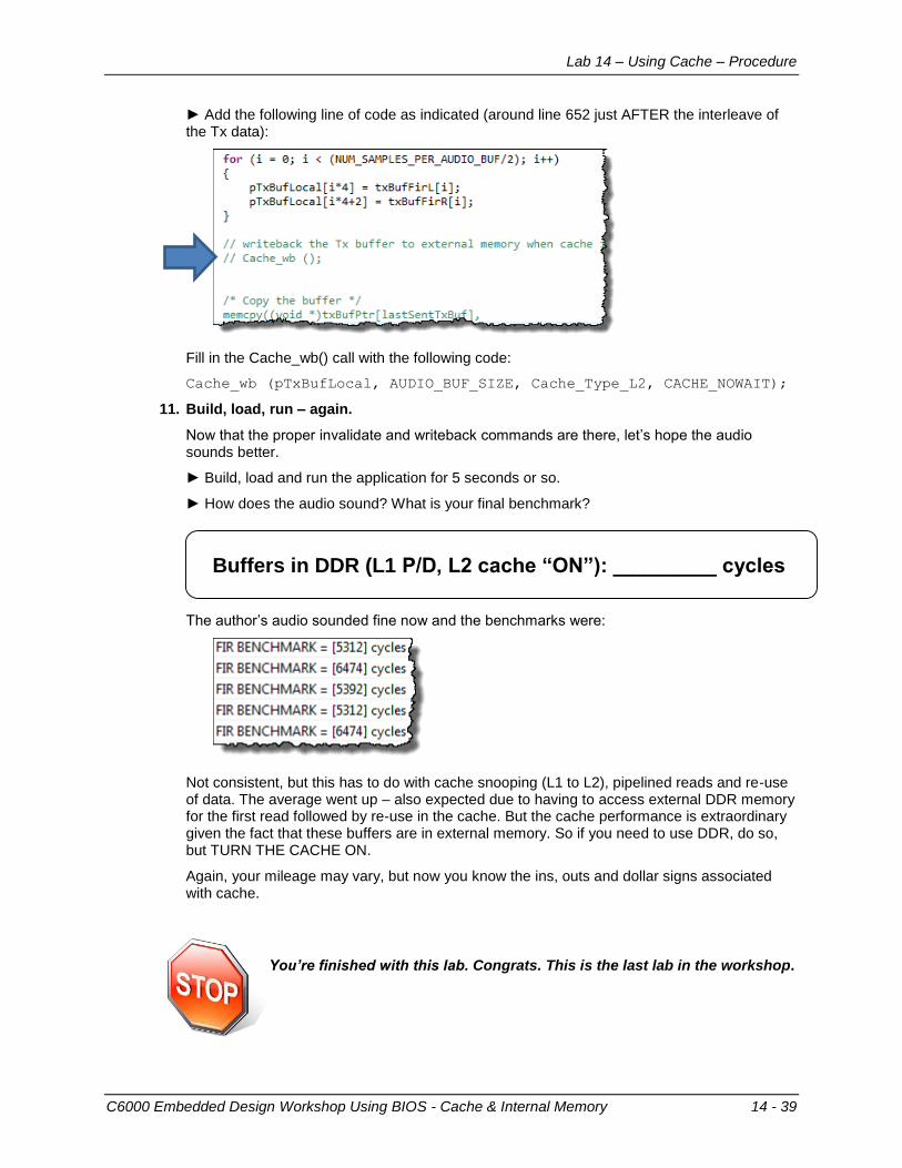
Lab 14 – Using Cache – Procedure
C6000 Embedded Design Workshop Using BIOS - Cache & Internal Memory 14 - 39
► Add the following line of code as indicated (around line 652 just AFTER the interleave of the Tx data):
Fill in the Cache_wb() call with the following code:
Cache_wb (pTxBufLocal, AUDIO_BUF_SIZE, Cache_Type_L2, CACHE_NOWAIT);
11. Build, load, run – again.
Now that the proper invalidate and writeback commands are there, let’s hope the audio sounds better.
► Build, load and run the application for 5 seconds or so.
► How does the audio sound? What is your final benchmark?
Buffers in DDR (L1 P/D, L2 cache “ON”): _________ cycles
The author’s audio sounded fine now and the benchmarks were:
Not consistent, but this has to do with cache snooping (L1 to L2), pipelined reads and re-use of data. The average went up – also expected due to having to access external DDR memory for the first read followed by re-use in the cache. But the cache performance is extraordinary given the fact that these buffers are in external memory. So if you need to use DDR, do so, but TURN THE CACHE ON.
Again, your mileage may vary, but now you know the ins, outs and dollar signs associated with cache.
You’re finished with this lab. Congrats. This is the last lab in the workshop.
Notes
14 - 40 C6000 Embedded Design Workshop Using BIOS - Cache & Internal Memory
Notes
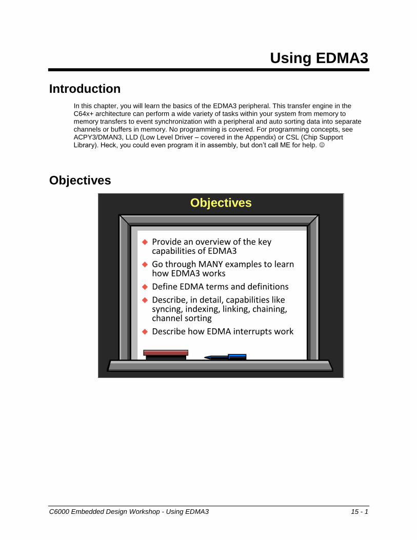
C6000 Embedded Design Workshop - Using EDMA3 15 - 1
Using EDMA3
Introduction
In this chapter, you will learn the basics of the EDMA3 peripheral. This transfer engine in the C64x+ architecture can perform a wide variety of tasks within your system from memory to memory transfers to event synchronization with a peripheral and auto sorting data into separate channels or buffers in memory. No programming is covered. For programming concepts, see ACPY3/DMAN3, LLD (Low Level Driver – covered in the Appendix) or CSL (Chip Support Library). Heck, you could even program it in assembly, but don’t call ME for help.
Objectives
Objectives
Provide an overview of the key capabilities of EDMA3
Go through MANY examples to learn how EDMA3 works
Define EDMA terms and definitions
Describe, in detail, capabilities like syncing, indexing, linking, chaining, channel sorting
Describe how EDMA interrupts work
Module Topics
15 - 2 C6000 Embedded Design Workshop - Using EDMA3
Module Topics
Using EDMA3 ............................................................................................................................. 15-1
Module Topics ......................................................................................................................... 15-2
Overview ................................................................................................................................. 15-3 What is a “DMA” ? ............................................................................................................... 15-3 Multiple “DMAs” ................................................................................................................... 15-4 EDMA3 in C64x+ Device .................................................................................................... 15-5
Terminology ............................................................................................................................ 15-6 Overview ............................................................................................................................. 15-6 Element, Frame, Block – ACNT, BCNT, CCNT .................................................................. 15-7 Simple Example .................................................................................................................. 15-7 Channels and PARAM Sets ................................................................................................ 15-8
Examples ................................................................................................................................ 15-9
Synchronization ..................................................................................................................... 15-12
Indexing ................................................................................................................................. 15-13
Events – Transfers – Actions ................................................................................................ 15-15 Overview ........................................................................................................................... 15-15 Triggers ............................................................................................................................. 15-16 Actions – Transfer Complete Code ................................................................................... 15-16
EDMA Interrupt Generation .................................................................................................. 15-17
Linking ................................................................................................................................... 15-18
Chaining ................................................................................................................................ 15-19
Channel Sorting .................................................................................................................... 15-21
Architecture & Optimization .................................................................................................. 15-22
Programming EDMA3 – Using Low Level Driver (LLD) ........................................................ 15-23
Chapter Quiz ......................................................................................................................... 15-25 Quiz – Answers ................................................................................................................. 15-26
Additional Information ........................................................................................................... 15-27
Notes ..................................................................................................................................... 15-28
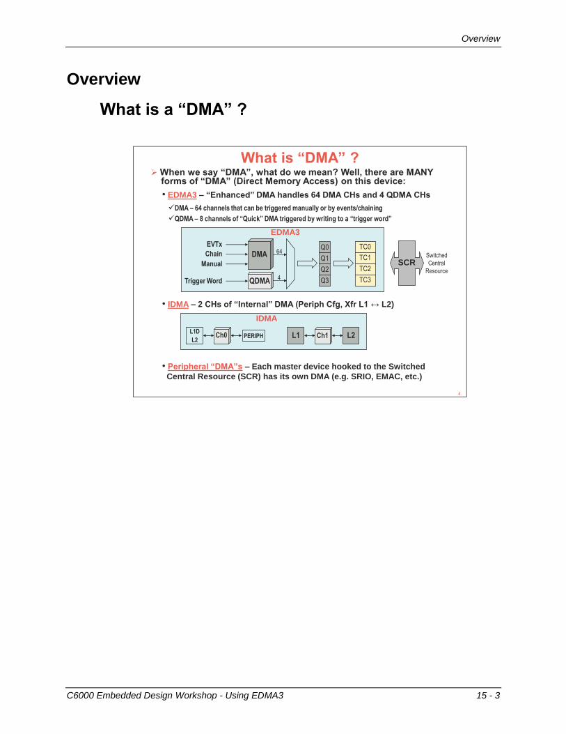
Overview
C6000 Embedded Design Workshop - Using EDMA3 15 - 3
Overview
What is a “DMA” ?
What is “DMA” ? When we say “DMA”, what do we mean? Well, there are MANY
forms of “DMA” (Direct Memory Access) on this device:
• EDMA3 – “Enhanced” DMA handles 64 DMA CHs and 4 QDMA CHs
DMA – 64 channels that can be triggered manually or by events/chaining
QDMA – 8 channels of “Quick” DMA triggered by writing to a “trigger word”
• IDMA – 2 CHs of “Internal” DMA (Periph Cfg, Xfr L1 ↔ L2)
• Peripheral “DMA”s – Each master device hooked to the Switched
Central Resource (SCR) has its own DMA (e.g. SRIO, EMAC, etc.)
Ch0L1D
L2PERIPH Ch1L1 L2
IDMA
Q0
Q1
Q2
Q3
TC0
TC1
TC2
TC3
SCR
QDMA
EVTx
Chain
Manual
EDMA3
DMA
Trigger Word
Switched
Central
Resource
64
4
4
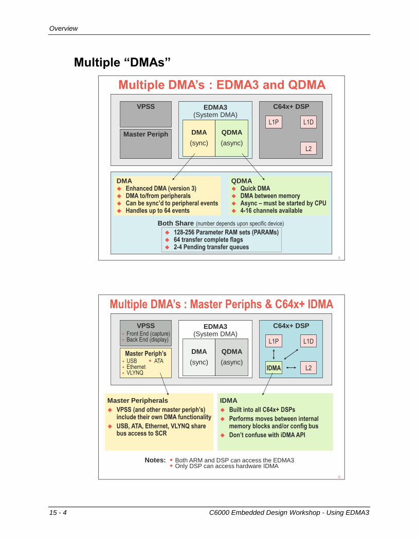
Overview
15 - 4 C6000 Embedded Design Workshop - Using EDMA3
Multiple “DMAs”
Multiple DMA’s : EDMA3 and QDMA
VPSS C64x+ DSP
L1P L1D
L2
EDMA3(System DMA)
DMA
(sync)
QDMA
(async)
DMA Enhanced DMA (version 3) DMA to/from peripherals Can be sync’d to peripheral events Handles up to 64 events
QDMA Quick DMA DMA between memory Async – must be started by CPU 4-16 channels available
128-256 Parameter RAM sets (PARAMs) 64 transfer complete flags 2-4 Pending transfer queues
Both Share (number depends upon specific device)
Master Periph
5
Multiple DMA’s : Master Periphs & C64x+ IDMA
C64x+ DSP
L1P L1D
L2IDMA
EDMA3(System DMA)
DMA
(sync)
QDMA
(async)
IDMA
Built into all C64x+ DSPs
Performs moves between internal memory blocks and/or config bus
Don’t confuse with iDMA API
VPSS
Master Periph’s
Front End (capture) Back End (display)
USB ATA Ethernet VLYNQ
Master Peripherals
VPSS (and other master periph’s) include their own DMA functionality
USB, ATA, Ethernet, VLYNQ share bus access to SCR
Notes: Both ARM and DSP can access the EDMA3 Only DSP can access hardware IDMA
6
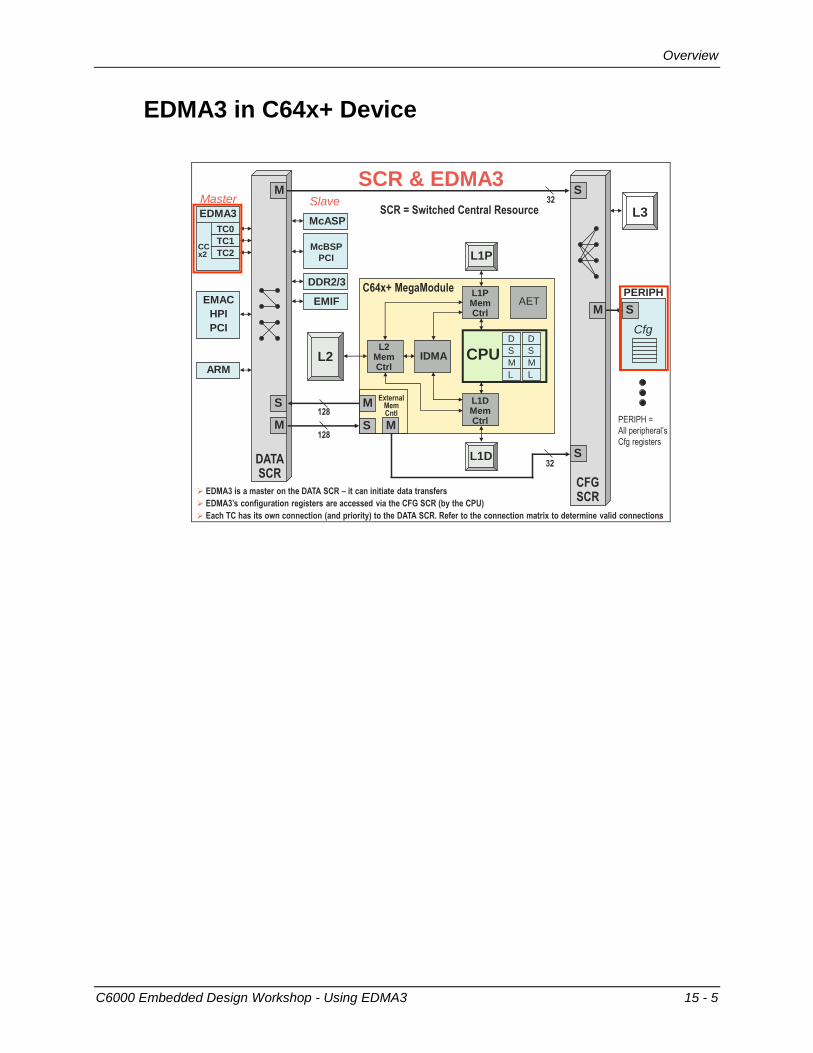
Overview
C6000 Embedded Design Workshop - Using EDMA3 15 - 5
EDMA3 in C64x+ Device
SCR & EDMA3
EDMA3
TC0
TC1
TC2
EMAC
HPI
PCI
ARM
McASP
McBSP
PCI
DDR2/3
L2MemCtrl
L2
L1P
L1D
D
S
M
L
D
S
M
L
CPU
C64x+ MegaModule
M
S
S
M M
S
IDMA
L1PMemCtrl
L1DMemCtrl
AET
DATASCR
CFGSCR
EMIF
128
128
Cfg
PERIPH
M S
M SMaster Slave
EDMA3 is a master on the DATA SCR – it can initiate data transfers
EDMA3’s configuration registers are accessed via the CFG SCR (by the CPU)
Each TC has its own connection (and priority) to the DATA SCR. Refer to the connection matrix to determine valid connections
32
PERIPH =
All peripheral’s
Cfg registers
SCR = Switched Central Resource32
ExternalMemCntl
CCx2
L3
7
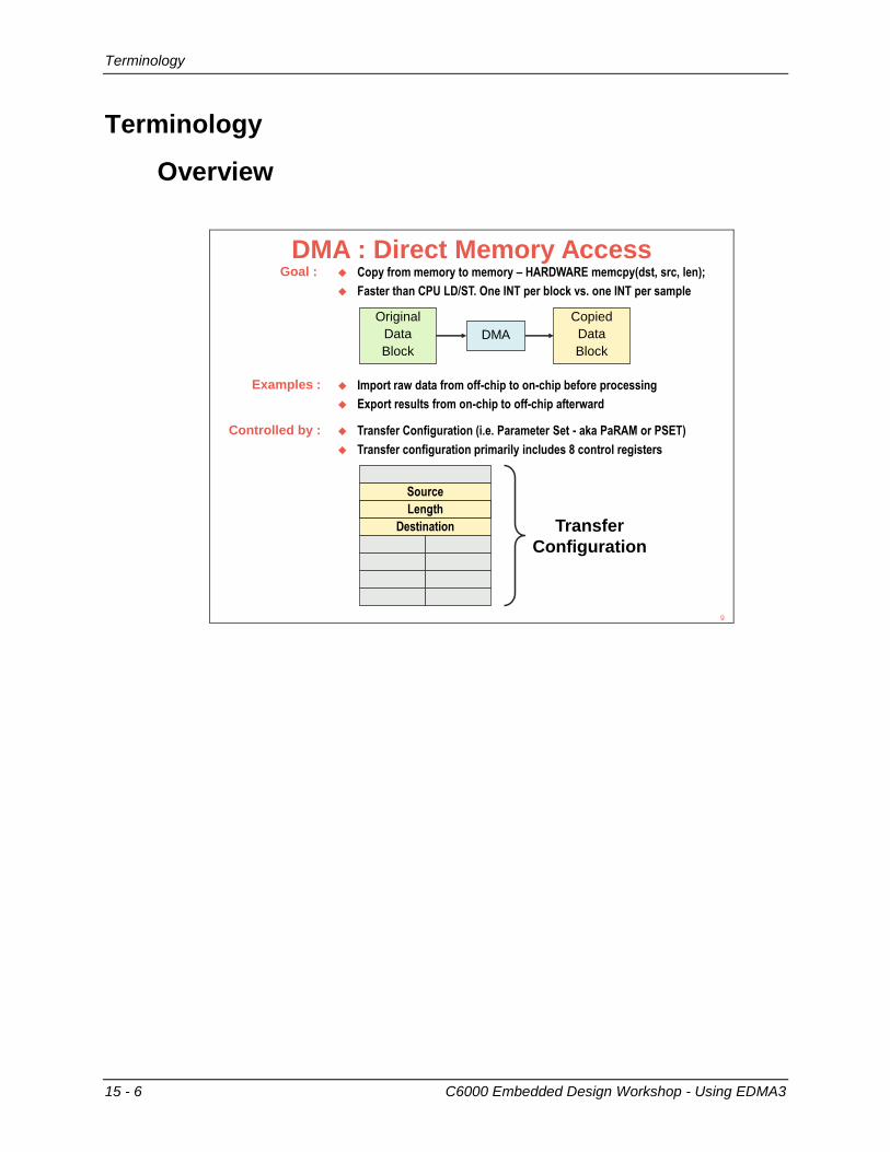
Terminology
15 - 6 C6000 Embedded Design Workshop - Using EDMA3
Terminology
Overview
DMA : Direct Memory Access Copy from memory to memory – HARDWARE memcpy(dst, src, len);
Faster than CPU LD/ST. One INT per block vs. one INT per sample
Import raw data from off-chip to on-chip before processing
Export results from on-chip to off-chip afterward
Transfer Configuration (i.e. Parameter Set - aka PaRAM or PSET)
Transfer configuration primarily includes 8 control registers
Goal :
Examples :
Controlled by :
Original
Data
Block
Copied
Data
Block
DMA
Transfer
Configuration
Source
ACNT
Destination
BCNTLength
9
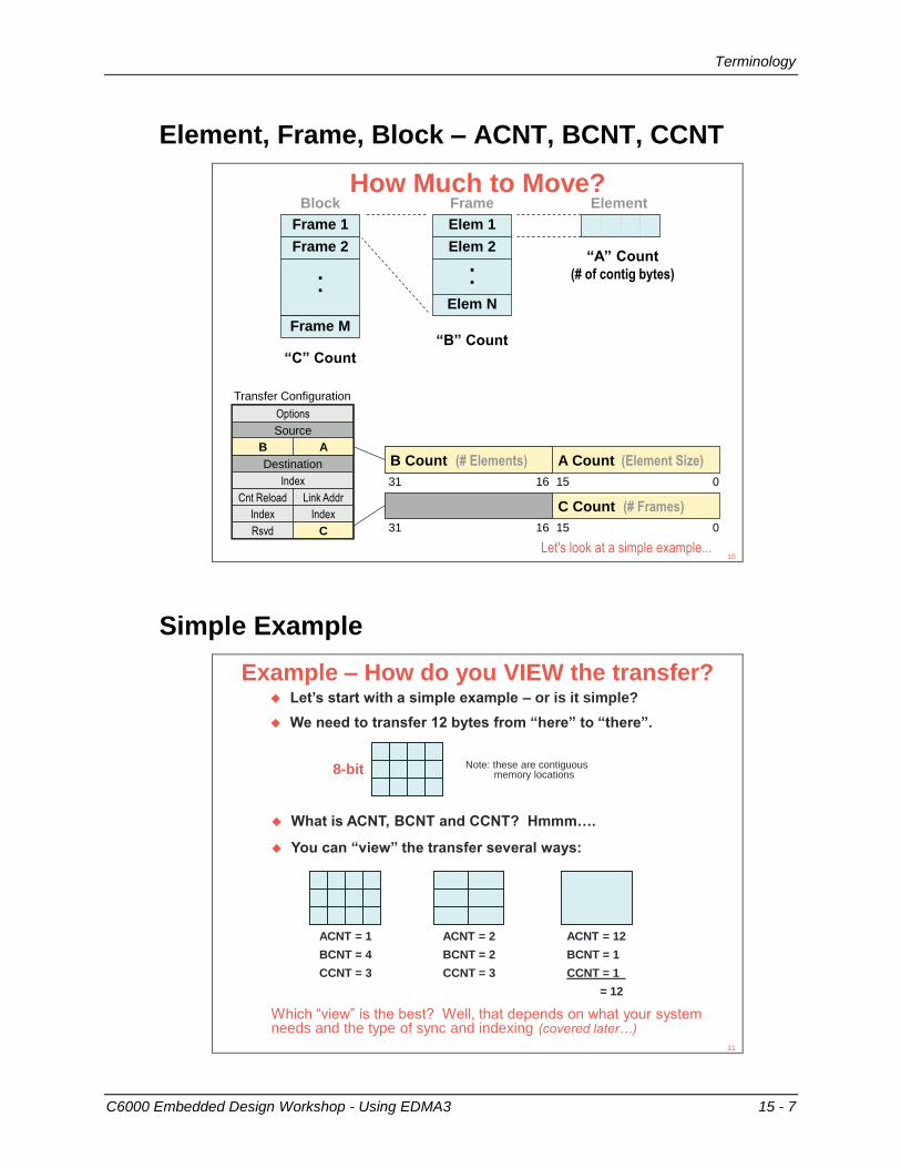
Terminology
C6000 Embedded Design Workshop - Using EDMA3 15 - 7
Element, Frame, Block – ACNT, BCNT, CCNT
How Much to Move?Element
(# of contig bytes)
A Count (Element Size)
015
Options
Source
Destination
Index
Link AddrCnt Reload
Transfer Count
“A” Count
1631
B Count (# Elements)
Elem 1
Elem 2
Elem N
Frame
.
.
“B” Count
IndexIndex
CRsvd
Frame 1
Frame 2
Frame M
Block
.
.
“C” Count
C Count (# Frames)
0151631
AB
Transfer Configuration
Let's look at a simple example...10
Simple Example
Example – How do you VIEW the transfer?
ACNT = 2
BCNT = 2
CCNT = 3
ACNT = 1
BCNT = 4
CCNT = 3
ACNT = 12
BCNT = 1
CCNT = 1
= 12
8-bit
Let’s start with a simple example – or is it simple?
We need to transfer 12 bytes from “here” to “there”.
What is ACNT, BCNT and CCNT? Hmmm….
You can “view” the transfer several ways:
Which “view” is the best? Well, that depends on what your systemneeds and the type of sync and indexing (covered later…)
Note: these are contiguousmemory locations
11
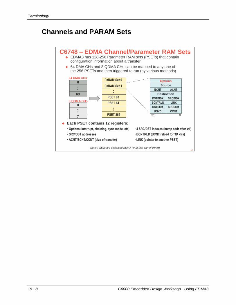
Terminology
15 - 8 C6000 Embedded Design Workshop - Using EDMA3
Channels and PARAM Sets
C6748 – EDMA Channel/Parameter RAM Sets EDMA3 has 128-256 Parameter RAM sets (PSETs) that contain
configuration information about a transfer
64 DMA CHs and 8 QDMA CHs can be mapped to any one ofthe 256 PSETs and then triggered to run (by various methods)
PaRAM Set 0
PaRAM Set 1
PSET 63
PSET 64
PSET 255
..
..31 0
Options
Source
Destination
CCNTRSVD
ACNTBCNT
SRCBIDXDSTBIDX
LINKBCNTRLD
SRCCIDXDSTCIDX
Each PSET contains 12 registers:
• Options (interrupt, chaining, sync mode, etc)
• SRC/DST addresses
• ACNT/BCNT/CCNT (size of transfer)
• 4 SRC/DST Indexes (bump addr after xfr)
• BCNTRLD (BCNT reload for 3D xfrs)
• LINK (pointer to another PSET)
.
.63
64 DMA CHs
0
0..7
8 QDMA CHs
Note: PSETs are dedicated EDMA RAM (not part of IRAM)12
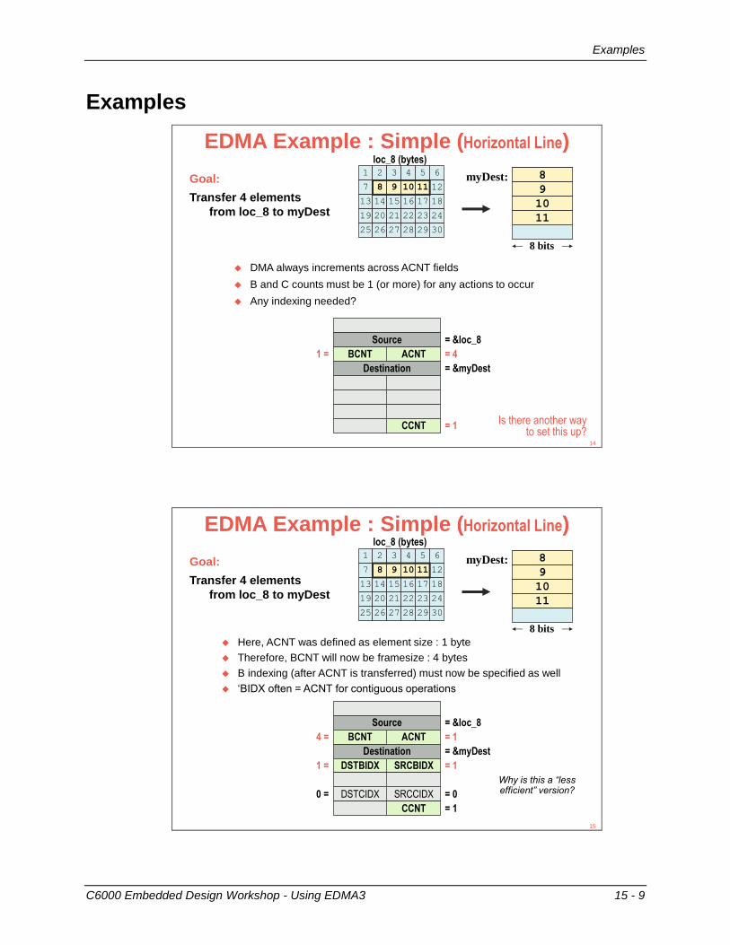
Examples
C6000 Embedded Design Workshop - Using EDMA3 15 - 9
Examples
EDMA Example : Simple (Horizontal Line)
myDest:
8 bits
8
9
10
11
loc_8 (bytes)1 2 3 4 5 6
7 12
13 14 15 16 17 18
19 20 21 22 23 24
25 26 27 28 29 30
8 9 10 118 9 10 11
8
9
10
11
Goal:
Transfer 4 elements
from loc_8 to myDest
= 41 =
Source
ACNT
Destination
BCNT
CCNT = 1
= &myDest
= &loc_8
DMA always increments across ACNT fields
B and C counts must be 1 (or more) for any actions to occur
Any indexing needed?
Is there another wayto set this up?
14
EDMA Example : Simple (Horizontal Line)
myDest:
8 bits
8
9
10
11
loc_8 (bytes)
1 2 3 4 5 6
7 12
13 14 15 16 17 18
19 20 21 22 23 24
25 26 27 28 29 30
8 9 10 118 9 10 11
8
9
10
11
Goal:
Transfer 4 elements
from loc_8 to myDest
= 14 =
= 11 =
= 00 =
= 1
= &myDest
= &loc_8
Here, ACNT was defined as element size : 1 byte
Therefore, BCNT will now be framesize : 4 bytes
B indexing (after ACNT is transferred) must now be specified as well
‘BIDX often = ACNT for contiguous operations
Why is this a “lessefficient” version?
Source
ACNT
Destination
SRCBIDX
BCNT
DSTBIDX
SRCCIDXDSTCIDX
CCNT
15
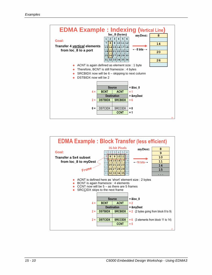
Examples
15 - 10 C6000 Embedded Design Workshop - Using EDMA3
EDMA Example : Indexing (Vertical Line)
1 2 3 4 5 6
7 8 9 10 11 12
13 14 15 16 17 18
19 20 21 22 23 24
25 26 27 28 29 30
myDest:
8 bits
= 14 =
= 62 =
= 00 =
= 1
= &myDest
= &loc_8
Goal:
Transfer 4 vertical elements
from loc_8 to a port
loc_8 (bytes)
ACNT is again defined as element size : 1 byte
Therefore, BCNT is still framesize : 4 bytes
SRCBIDX now will be 6 – skipping to next column
DSTBIDX now will be 2
Source
ACNT
Destination
SRCBIDX
BCNT
DSTBIDX
SRCCIDXDSTCIDX
CCNT
31 32 33 34 35 36
8
14
20
26
16
EDMA Example : Block Transfer (less efficient)
1 2 3 4 5 6
7 8 9 10 11 12
13 14 15 16 17 18
19 20 21 22 23 24
25 26 27 28 29 30
31 32 33 34 35 36
myDest:16-bit Pixels
16 bits
Goal:
Transfer a 5x4 subset
from loc_8 to myDest
= &myDest
= &loc_8
= 24 =
= 2 (2 bytes going from block 8 to 9)2 =
= 6 (3 elements from block 11 to 14)2 =
= 5
ACNT is defined here as ‘short’ element size : 2 bytes BCNT is again framesize : 4 elements CCNT now will be 5 – as there are 5 frames SRCCIDX skips to the next frame
8
9
10
11
14
15
...
Source
ACNT
Destination
SRCBIDX
BCNT
DSTBIDX
SRCCIDXDSTCIDX
CCNT
17
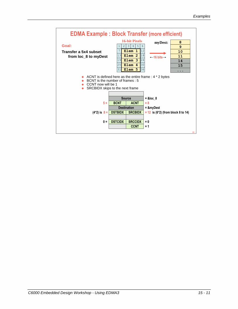
Examples
C6000 Embedded Design Workshop - Using EDMA3 15 - 11
EDMA Example : Block Transfer (more efficient)
1 2 3 4 5 6
7 8 9 10 11 12
13 14 15 16 17 18
19 20 21 22 23 24
25 26 27 28 29 30
31 32 33 34 35 36
myDest:16-bit Pixels
16 bits
Goal:
Transfer a 5x4 subset
from loc_8 to myDest
= &myDest
= &loc_8
= 85 =
= 12 is (6*2) (from block 8 to 14)(4*2) is 8 =
= 00 =
= 1
ACNT is defined here as the entire frame : 4 * 2 bytes BCNT is the number of frames : 5 CCNT now will be 1 SRCBIDX skips to the next frame
8
9
10
11
14
15
...
Source
ACNT
Destination
SRCBIDX
BCNT
DSTBIDX
SRCCIDXDSTCIDX
CCNT
Elem 1
Elem 2
Elem 3
Elem 4
Elem 5
18
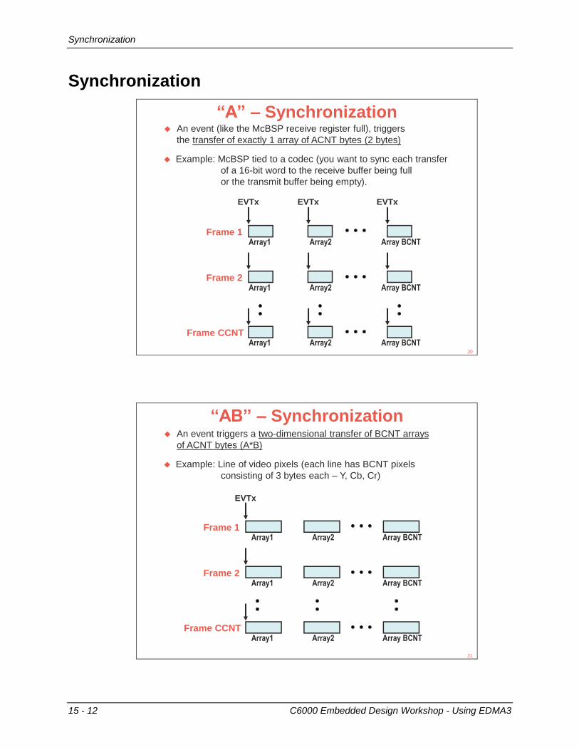
Synchronization
15 - 12 C6000 Embedded Design Workshop - Using EDMA3
Synchronization
“A” – Synchronization An event (like the McBSP receive register full), triggers
the transfer of exactly 1 array of ACNT bytes (2 bytes)
Example: McBSP tied to a codec (you want to sync each transfer
of a 16-bit word to the receive buffer being full
or the transmit buffer being empty).
Frame 1Array1 Array2 Array BCNT
Frame 2Array1 Array2 Array BCNT
Frame CCNTArray1 Array2 Array BCNT
EVTx EVTx EVTx
20
“AB” – Synchronization An event triggers a two-dimensional transfer of BCNT arrays
of ACNT bytes (A*B)
Example: Line of video pixels (each line has BCNT pixels
consisting of 3 bytes each – Y, Cb, Cr)
Frame 1Array1 Array2 Array BCNT
Frame 2Array1 Array2 Array BCNT
Frame CCNTArray1 Array2 Array BCNT
EVTx
21
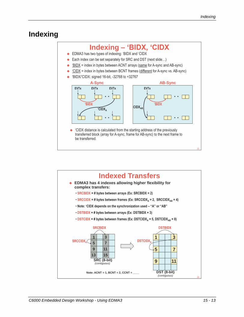
Indexing
C6000 Embedded Design Workshop - Using EDMA3 15 - 13
Indexing
Indexing – ‘BIDX, ‘CIDX EDMA3 has two types of indexing: ‘BIDX and ‘CIDX
Each index can be set separately for SRC and DST (next slide…)
‘BIDX = index in bytes between ACNT arrays (same for A-sync and AB-sync)
‘CIDX = index in bytes between BCNT frames (different for A-sync vs. AB-sync)
‘BIDX/’CIDX: signed 16-bit, -32768 to +32767
‘CIDX distance is calculated from the starting address of the previouslytransferred block (array for A-sync, frame for AB-sync) to the next frame tobe transferred.
. .
EVTx EVTx EVTx
. .
‘BIDX
‘CIDXA
A-Sync
. .
EVTx
. .
‘BIDXCIDXAB
AB-Sync
23
Indexed Transfers
1 3
9 11
5 7
13 15
1 3
5 7
9 11
EDMA3 has 4 indexes allowing higher flexibility forcomplex transfers:
• SRCBIDX = # bytes between arrays (Ex: SRCBIDX = 2)
• SRCCIDX = # bytes between frames (Ex: SRCCIDXA = 2, SRCCIDXAB = 4)
• Note: ‘CIDX depends on the synchronization used – “A” or “AB”
• DSTBIDX = # bytes between arrays (Ex: DSTBIDX = 3)
• DSTCIDX = # bytes between frames (Ex: DSTCIDXA = 5, DSTCIDXAB = 8)
SRC (8-bit)
DST (8-bit)
SRCBIDX
SRCCIDXA
DSTBIDX
DSTCIDXA
Note: ACNT = 1, BCNT = 2, CCNT = ____
(contiguous)
(contiguous)24
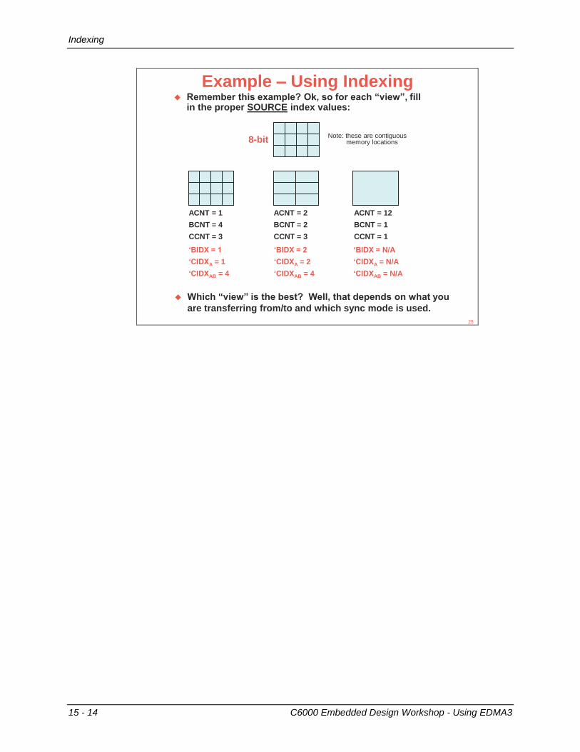
Indexing
15 - 14 C6000 Embedded Design Workshop - Using EDMA3
Example – Using Indexing
ACNT = 2
BCNT = 2
CCNT = 3
ACNT = 1
BCNT = 4
CCNT = 3
ACNT = 12
BCNT = 1
CCNT = 1
8-bit
Remember this example? Ok, so for each “view”, fillin the proper SOURCE index values:
Which “view” is the best? Well, that depends on what you
are transferring from/to and which sync mode is used.
‘BIDX = 1
‘CIDXA = 1
‘CIDXAB = 4
‘BIDX = 2
‘CIDXA = 2
‘CIDXAB = 4
‘BIDX = N/A
‘CIDXA = N/A
‘CIDXAB = N/A
Note: these are contiguousmemory locations
25
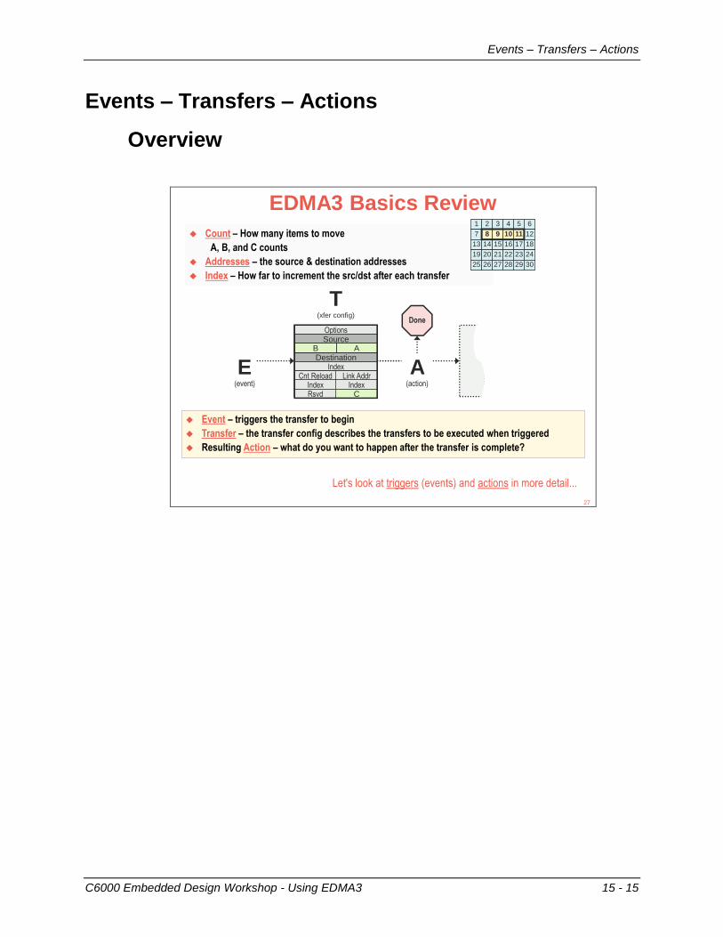
Events – Transfers – Actions
C6000 Embedded Design Workshop - Using EDMA3 15 - 15
Events – Transfers – Actions
Overview
EDMA3 Basics Review
Event – triggers the transfer to begin
Transfer – the transfer config describes the transfers to be executed when triggered
Resulting Action – what do you want to happen after the transfer is complete?
Count – How many items to move
A, B, and C counts
Addresses – the source & destination addresses
Index – How far to increment the src/dst after each transfer
1 2 3 4 5 6
7 12
13 14 15 16 17 18
19 20 21 22 23 24
25 26 27 28 29 30
8 9 10 118 9 10 11
T(xfer config)
E(event)
Done
A(action)
OptionsSource
DestinationIndex
Link AddrCnt Reload
Transfer Count
IndexIndexCRsvd
AB
T(xfer config)
Let's look at triggers (events) and actions in more detail...
27
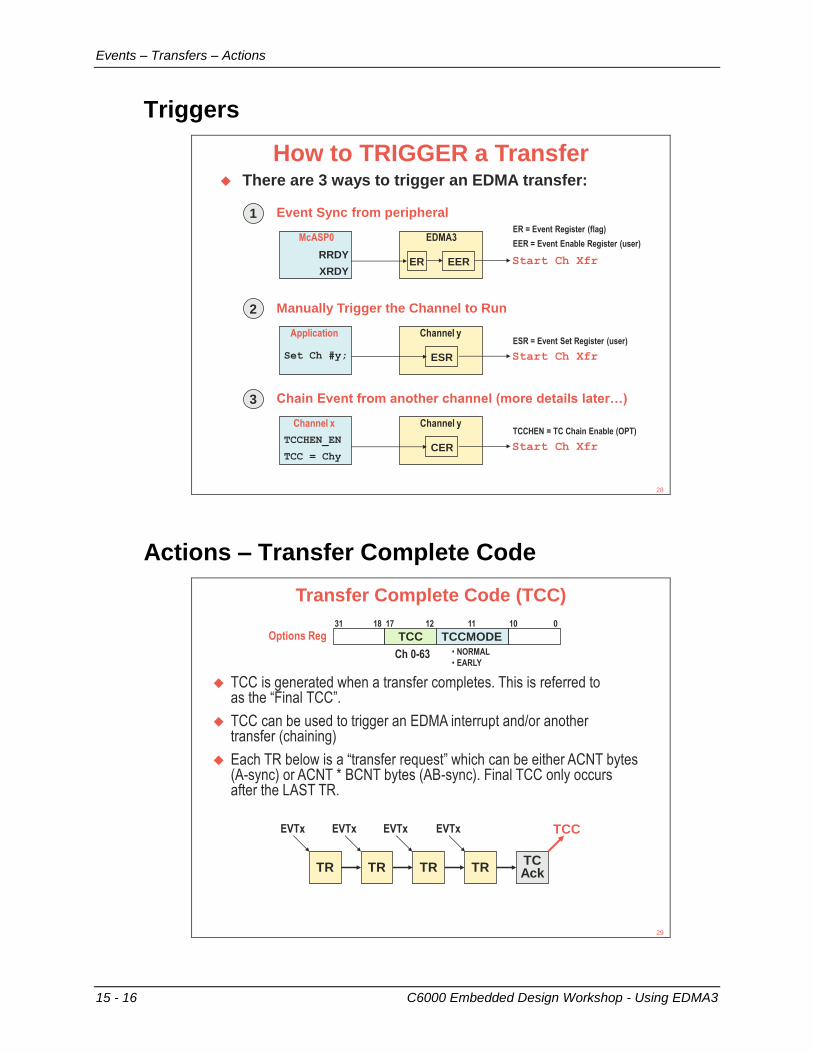
Events – Transfers – Actions
15 - 16 C6000 Embedded Design Workshop - Using EDMA3
Triggers
How to TRIGGER a Transfer There are 3 ways to trigger an EDMA transfer:
1 Event Sync from peripheral
RRDY
XRDY
McASP0 EDMA3
ER EER Start Ch Xfr
2 Manually Trigger the Channel to Run
Application Channel y
ESR Start Ch XfrSet Ch #y;
ER = Event Register (flag)
EER = Event Enable Register (user)
ESR = Event Set Register (user)
3 Chain Event from another channel (more details later…)
Channel x Channel y
CER Start Ch XfrTCCHEN_EN
TCC = Chy
TCCHEN = TC Chain Enable (OPT)
28
Actions – Transfer Complete Code
Transfer Complete Code (TCC)
TCC is generated when a transfer completes. This is referred toas the “Final TCC”.
TCC can be used to trigger an EDMA interrupt and/or anothertransfer (chaining)
Each TR below is a “transfer request” which can be either ACNT bytes(A-sync) or ACNT * BCNT bytes (AB-sync). Final TCC only occurs after the LAST TR.
TR TR TR TRTCAck
EVTx EVTx EVTx EVTx TCC
31 18 17 12
Options Reg TCC TCCMODE
11 10 0
Ch 0-63 • NORMAL
• EARLY
29
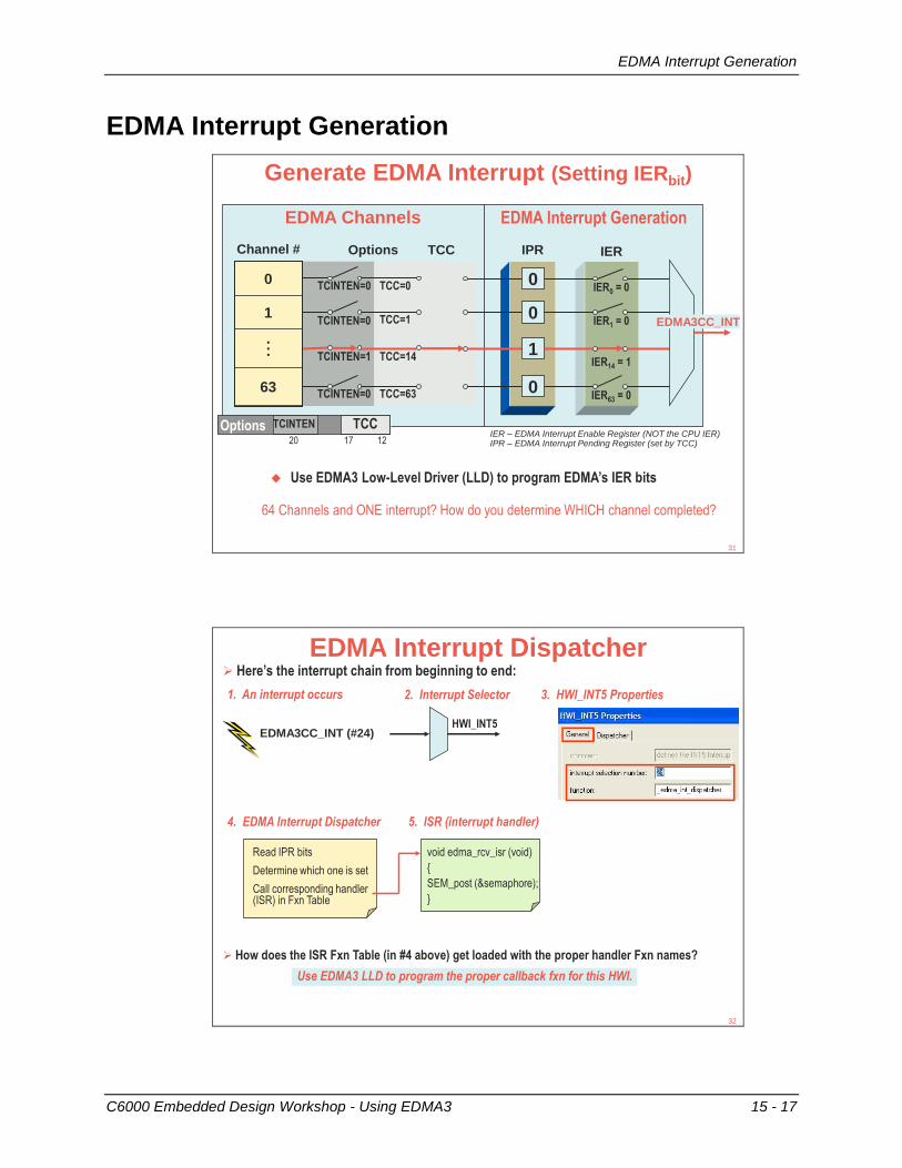
EDMA Interrupt Generation
C6000 Embedded Design Workshop - Using EDMA3 15 - 17
EDMA Interrupt Generation
Generate EDMA Interrupt (Setting IERbit)
EDMA Channels
Channel #
TCINTEN=0
TCINTEN=0
TCINTEN=1
TCINTEN=0
TCC=0
TCC=1
TCC=14
TCC=6363
...
1
0
Options
Options TCCTCINTEN
20 17 12
EDMA Interrupt Generation
0
0
1
0
IPR
IER0 = 0
IER1 = 0
IER14 = 1
IER63 = 0
IER
EDMA3CC_INT
TCC
Use EDMA3 Low-Level Driver (LLD) to program EDMA’s IER bits
IER – EDMA Interrupt Enable Register (NOT the CPU IER)IPR – EDMA Interrupt Pending Register (set by TCC)
64 Channels and ONE interrupt? How do you determine WHICH channel completed?
31
EDMA Interrupt Dispatcher Here’s the interrupt chain from beginning to end:
Use EDMA3 LLD to program the proper callback fxn for this HWI.
EDMA3CC_INT (#24)
2. Interrupt Selector
HWI_INT5
1. An interrupt occurs 3. HWI_INT5 Properties
4. EDMA Interrupt Dispatcher
Read IPR bits
Determine which one is set
Call corresponding handler(ISR) in Fxn Table
5. ISR (interrupt handler)
void edma_rcv_isr (void)
{
SEM_post (&semaphore);
}
How does the ISR Fxn Table (in #4 above) get loaded with the proper handler Fxn names?
32
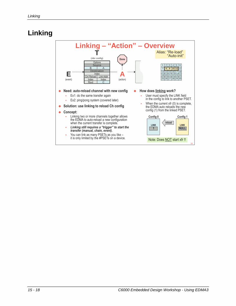
Linking
15 - 18 C6000 Embedded Design Workshop - Using EDMA3
Linking
Linking – “Action” – Overview
1 2 3 4 5 6
7 12
13 14 15 16 17 18
19 20 21 22 23 24
25 26 27 28 29 30
8 9 10 118 9 10 11
T(xfer config)
E(event)
Done
A(action)
OptionsSource
DestinationIndex
Link AddrCnt Reload
Transfer Count
IndexIndexCRsvd
AB
T(xfer config)
Need: auto-reload channel with new config
Ex1: do the same transfer again
Ex2: ping/pong system (covered later)
Solution: use linking to reload Ch config
Concept: Linking two or more channels together allows
the EDMA to auto-reload a new configurationwhen the current transfer is complete.
Linking still requires a “trigger” to start thetransfer (manual, chain, event).
You can link as many PSETs as you like –it is only limited by the #PSETs on a device.
How does linking work?
User must specify the LINK fieldin the config to link to another PSET.
When the current xfr (0) is complete,the EDMA auto reloads the newconfig (1) from the linked PSET.
1LINK
Config 0
NULLLINK
Config 1
reload
Alias: “Re-load”“Auto-init”
Note: Does NOT start xfr !!34
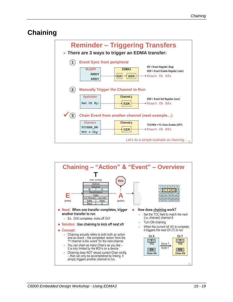
Chaining
C6000 Embedded Design Workshop - Using EDMA3 15 - 19
Chaining
Reminder – Triggering Transfers There are 3 ways to trigger an EDMA transfer:
1 Event Sync from peripheral
RRDY
XRDY
McASP0 EDMA3
ER EER Start Ch Xfr
2 Manually Trigger the Channel to Run
Application Channel y
ESR Start Ch XfrSet Ch #y;
ER = Event Register (flag)
EER = Event Enable Register (user)
ESR = Event Set Register (user)
3 Chain Event from another channel (next example…)
Channel x Channel y
CER Start Ch XfrTCCHEN_EN
TCC = Chy
TCCHEN = TC Chain Enable (OPT)
Let’s do a simple example on chaining…36
Chaining – “Action” & “Event” – Overview
1 2 3 4 5 6
7 12
13 14 15 16 17 18
19 20 21 22 23 24
25 26 27 28 29 30
8 9 10 118 9 10 11
T(xfer config)
E(event)
Done
A(action)
OptionsSource
DestinationIndex
Link AddrCnt Reload
Transfer Count
IndexIndexCRsvd
AB
T(xfer config)
Need: When one transfer completes, trigger another transfer to run
Ex: ChX completes, kicks off ChY
Solution: Use chaining to kick off next xfr
Concept: Chaining actually refers to both both an action
and an event – the completed ‘action’ from the 1st channel is the ‘event’ for the next channel
You can chain as many Chan’s as you like –it is only limited by the #Ch’s on a device
Chaining does NOT reload current Chan config – that can only be accomplished by linking. Itsimply triggers another channel to run.
How does chaining work?
Set the TCC field to match the next (i.e. chained) channel #
Turn ON chaining
When the current xfr (X) is complete,it triggers the next Ch (Y) to run
YTCC
Ch X
EN
Chain EN
?TCC
Ch Y
DIS
Chain EN
Done ?
RUN Y
37
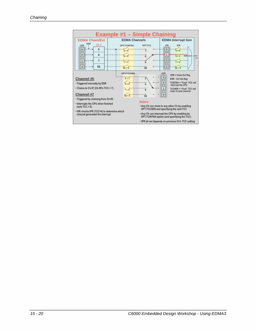
Chaining
15 - 20 C6000 Embedded Design Workshop - Using EDMA3
Example #1 – Simple ChainingEDMA Chain/Evt EDMA Interrupt GenEDMA Channels
5 = 0
6 = 1
7 = 0
55 = 0
0
1
0
0
IERIPR
EDMA3CC_GINT
Ch #
55
7
6
50
0
1
0
CER
5 = 0
6 = 0
7 = 1
55 = 0
5 = 1
6 = 0
7 = 0
55 = 0
OPT.TCCHEN
ESR
7
0
6
55
• Triggered manually by ESR
• Chains to Ch #7 (Ch #5’s TCC = 7)
0
0
1
0
CER
OPT.TCCOPT.TCINTEN
7
0
6
55
Channel #5
• Triggered by chaining from Ch #5
• Interrupts the CPU when finished(sets TCC = 6)
• ISR checks IPR (TCC=6) to determine whichchannel generated the interrupt
Channel #7
CER = Chain Evt Reg
ESR – Evt Set Reg
TCINTEN = “Final” TCC willinterrupt the CPU
TCCHEN = “Final” TCC willchain to next channel
• Any Ch can chain to any other Ch by enablingOPT.TCCHEN and specifying the next TCC
• Any Ch can interrupt the CPU by enabling itsOPT.TCINTEN option (and specifying the TCC)
• IPR bit set depends on previous Ch’s TCC setting
Notes:
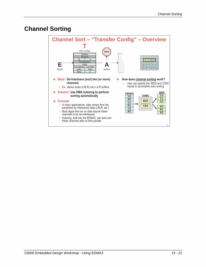
Channel Sorting
C6000 Embedded Design Workshop - Using EDMA3 15 - 21
Channel Sorting
Channel Sort – “Transfer Config” – Overview
1 2 3 4 5 6
7 12
13 14 15 16 17 18
19 20 21 22 23 24
25 26 27 28 29 30
8 9 10 118 9 10 11
T(xfer config)
E(event)
Done
A(action)
OptionsSource
DestinationIndex
Link AddrCnt Reload
Transfer Count
IndexIndexCRsvd
AB
T(xfer config)
Need: De-interleave (sort) two (or more)channels
Ex: stereo audio (LRLR) into L & R buffers
Solution: Use DMA indexing to performsorting automatically
Concept: In many applications, data comes from the
peripheral as interleaved data (LRLR, etc.)
Most algos that run on data require thesechannels to be de-interleaved
Indexing, built into the EDMA3, can auto-sortthese channels with no time penalty
How does channel sorting work?
User can specify the ‘BIDX and ‘CIDXvalues to accomplish auto sorting
L0R0L1R1L2R2
PERIPHEDMA
BIDX
CIDX
L0L1L2
R0R1R2
MEM
40
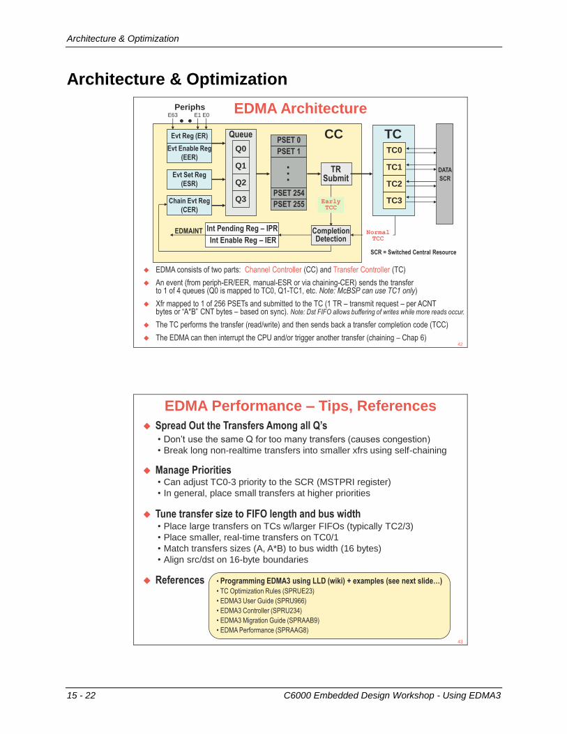
Architecture & Optimization
15 - 22 C6000 Embedded Design Workshop - Using EDMA3
Architecture & Optimization
EDMA Architecture
Evt Reg (ER)
Chain Evt Reg
(CER)
Evt Enable Reg
(EER)
Evt Set Reg
(ESR)
Q0
Q1
Q2
Q3
QueuePSET 0
PSET 1
PSET 254
PSET 255
TRSubmit
Periphs
CompletionDetection
Int Pending Reg – IPR
Int Enable Reg – IER
TC0
TC1
TC2
TC3
TC
EDMAINT
CC
EDMA consists of two parts: Channel Controller (CC) and Transfer Controller (TC)
An event (from periph-ER/EER, manual-ESR or via chaining-CER) sends the transferto 1 of 4 queues (Q0 is mapped to TC0, Q1-TC1, etc. Note: McBSP can use TC1 only)
Xfr mapped to 1 of 256 PSETs and submitted to the TC (1 TR – transmit request – per ACNTbytes or “A*B” CNT bytes – based on sync). Note: Dst FIFO allows buffering of writes while more reads occur.
The TC performs the transfer (read/write) and then sends back a transfer completion code (TCC)
The EDMA can then interrupt the CPU and/or trigger another transfer (chaining – Chap 6)
SCR = Switched Central Resource
.
.
.
EarlyTCC
NormalTCC
E0E1E63
DATA
SCR
42
EDMA Performance – Tips, References
Spread Out the Transfers Among all Q’s
• Programming EDMA3 using LLD (wiki) + examples (see next slide…)
• TC Optimization Rules (SPRUE23)
• EDMA3 User Guide (SPRU966)
• EDMA3 Controller (SPRU234)
• EDMA3 Migration Guide (SPRAAB9)
• EDMA Performance (SPRAAG8)
• Don’t use the same Q for too many transfers (causes congestion)
• Break long non-realtime transfers into smaller xfrs using self-chaining
Manage Priorities• Can adjust TC0-3 priority to the SCR (MSTPRI register)
• In general, place small transfers at higher priorities
Tune transfer size to FIFO length and bus width• Place large transfers on TCs w/larger FIFOs (typically TC2/3)
• Place smaller, real-time transfers on TC0/1
• Match transfers sizes (A, A*B) to bus width (16 bytes)
• Align src/dst on 16-byte boundaries
References
43
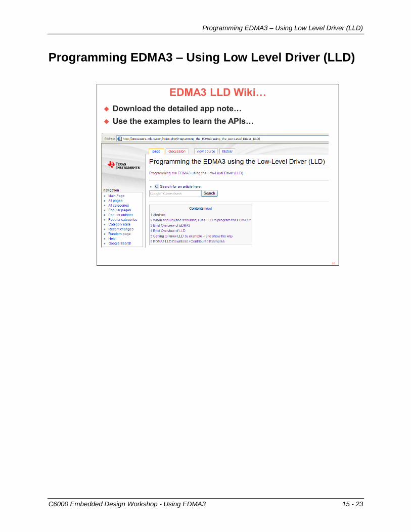
Programming EDMA3 – Using Low Level Driver (LLD)
C6000 Embedded Design Workshop - Using EDMA3 15 - 23
Programming EDMA3 – Using Low Level Driver (LLD)
EDMA3 LLD Wiki…
Download the detailed app note…
Use the examples to learn the APIs…
44
Programming EDMA3 – Using Low Level Driver (LLD)
15 - 24 C6000 Embedded Design Workshop - Using EDMA3
*** this page used to have very valuable information on it ***
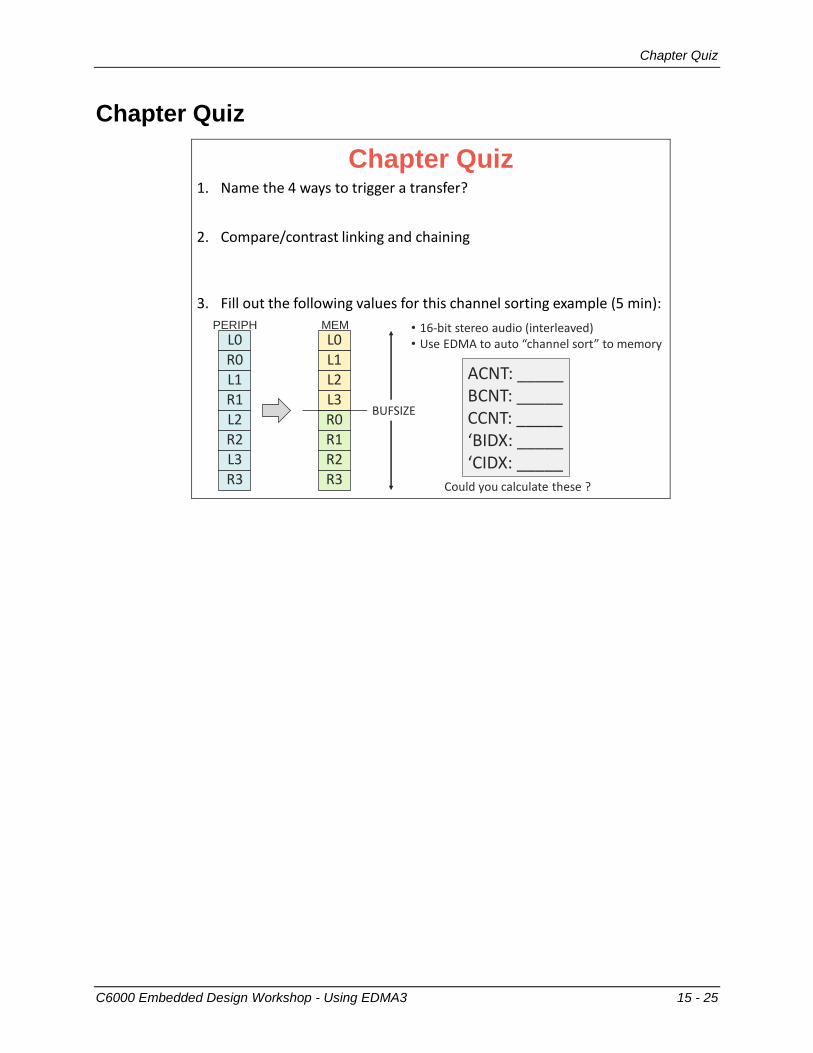
Chapter Quiz
C6000 Embedded Design Workshop - Using EDMA3 15 - 25
Chapter Quiz
Chapter Quiz
L0R0L1R1L2R2L3R3
• 16-bit stereo audio (interleaved)• Use EDMA to auto “channel sort” to memoryL0
L1L2L3R0R1R2R3
ACNT: _____BCNT: _____CCNT: _____‘BIDX: _____‘CIDX: _____
PERIPH MEM
Could you calculate these ?
BUFSIZE
1. Name the 4 ways to trigger a transfer?
2. Compare/contrast linking and chaining
3. Fill out the following values for this channel sorting example (5 min):
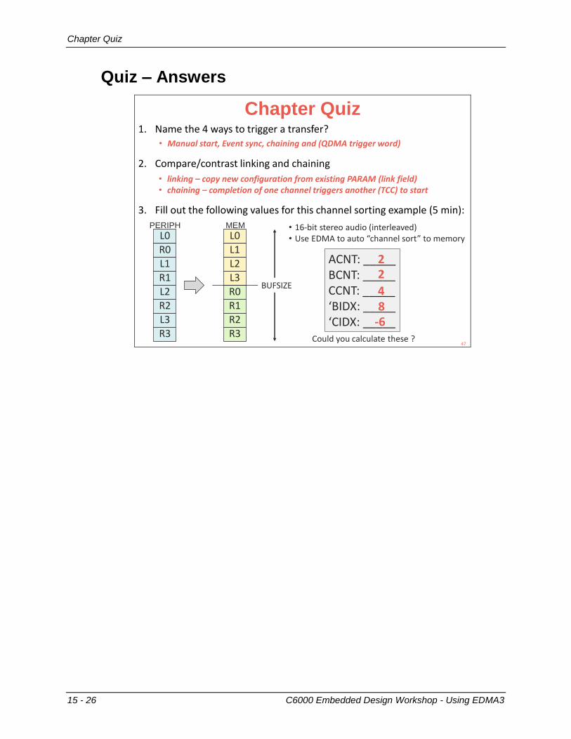
Chapter Quiz
15 - 26 C6000 Embedded Design Workshop - Using EDMA3
Quiz – Answers
Chapter Quiz1. Name the 4 ways to trigger a transfer?
2. Compare/contrast linking and chaining
3. Fill out the following values for this channel sorting example (5 min):
• Manual start, Event sync, chaining and (QDMA trigger word)
• linking – copy new configuration from existing PARAM (link field)• chaining – completion of one channel triggers another (TCC) to start
L0R0L1R1L2R2L3R3
• 16-bit stereo audio (interleaved)• Use EDMA to auto “channel sort” to memoryL0
L1L2L3R0R1R2R3
ACNT: _____BCNT: _____CCNT: _____‘BIDX: _____‘CIDX: _____
PERIPH MEM
22
48-6
Could you calculate these ?
BUFSIZE
47
Additional Information
C6000 Embedded Design Workshop - Using EDMA3 15 - 27
Additional Information
Notes
15 - 28 C6000 Embedded Design Workshop - Using EDMA3
Notes