C 797 ACTA - jultika.oulu.fi
84
UNIVERSITATIS OULUENSIS ACTA C TECHNICA OULU 2021 C 797 Joni Kilpijärvi RF-MICROWAVE SENSOR DEVELOPMENT FOR CELL AND HUMAN IN VITRO AND EX VIVO MONITORING UNIVERSITY OF OULU GRADUATE SCHOOL; UNIVERSITY OF OULU, FACULTY OF INFORMATION TECHNOLOGY AND ELECTRICAL ENGINEERING; LINKÖPING UNIVERSITY, DEPARTMENT OF PHYSICS, CHEMISTRY AND BIOLOGY (IFM); INFOTECH C 797 ACTA Joni Kilpijärvi
Transcript of C 797 ACTA - jultika.oulu.fi

UNIVERSITY OF OULU P .O. Box 8000 F I -90014 UNIVERSITY OF OULU FINLAND
A C T A U N I V E R S I T A T I S O U L U E N S I S
University Lecturer Tuomo Glumoff
University Lecturer Santeri Palviainen
Postdoctoral researcher Jani Peräntie
University Lecturer Anne Tuomisto
University Lecturer Veli-Matti Ulvinen
Planning Director Pertti Tikkanen
Professor Jari Juga
Associate Professor (tenure) Anu Soikkeli
University Lecturer Santeri Palviainen
Publications Editor Kirsti Nurkkala
ISBN 978-952-62-3033-7 (Paperback)ISBN 978-952-62-3034-4 (PDF)ISSN 0355-3213 (Print)ISSN 1796-2226 (Online)
U N I V E R S I TAT I S O U L U E N S I SACTAC
TECHNICA
U N I V E R S I TAT I S O U L U E N S I SACTAC
TECHNICA
OULU 2021
C 797
Joni Kilpijärvi
RF-MICROWAVE SENSOR DEVELOPMENT FOR CELL AND HUMAN IN VITRO AND EX VIVO MONITORING
UNIVERSITY OF OULU GRADUATE SCHOOL;UNIVERSITY OF OULU,FACULTY OF INFORMATION TECHNOLOGY AND ELECTRICAL ENGINEERING;LINKÖPING UNIVERSITY,DEPARTMENT OF PHYSICS, CHEMISTRY AND BIOLOGY (IFM);INFOTECH
C 797
AC
TAJoni K
ilpijärvi
C797etukansi.fm Page 1 Tuesday, August 17, 2021 1:51 PM


ACTA UNIVERS ITAT I S OULUENS I SC Te c h n i c a 7 9 7
JONI KILPIJÄRVI
RF-MICROWAVE SENSOR DEVELOPMENT FOR CELL AND HUMAN IN VITRO AND EX VIVO MONITORING
Academic dissertation to be presented with the assent ofthe Doctoral Training Committee of InformationTechnology and Electrical Engineering of the University ofOulu for public defence in Martti Ahtisaari auditorium(L2), Linnanmaa, on 22 October 2021, at 11 a.m.
UNIVERSITY OF OULU, OULU 2021

Copyright © 2021Acta Univ. Oul. C 797, 2021
Supervised byDocent Jari JuutiDoctor Niina HalonenDoctor Maciej SobocińskiProfessor Kajsa UvdalProfessor Anita Lloyd Spetz
Reviewed byProfessor Hong WangProfessor Mailadil Thomas Sebastian
ISBN 978-952-62-3033-7 (Paperback)ISBN 978-952-62-3034-4 (PDF)
ISSN 0355-3213 (Printed)ISSN 1796-2226 (Online)
Cover DesignRaimo Ahonen
PUNAMUSTATAMPERE 2021
OpponentDoctor Karol Malecha

Kilpijärvi, Joni, RF-microwave sensor development for cell and human in vitroand ex vivo monitoring. University of Oulu Graduate School; University of Oulu, Faculty of Information Technologyand Electrical Engineering; Linköping University, Department of Physics, Chemistry andBiology (IFM); InfotechActa Univ. Oul. C 797, 2021University of Oulu, P.O. Box 8000, FI-90014 University of Oulu, Finland
Abstract
In this research new RF/microwave-based sensor solutions were developed for the monitoring ofbiological cells and human beings to obtain a better understanding of their activity or state in aquick, cheap, easy and continuous way. The effect of different substances on cell behaviour canbe monitored by measuring the electrical environment where changes are observed as cells reactto a stimulus. The starting point of the study was a microchip with a capacitance measurementsystem integrated into the culturing chamber, enabling the monitoring of cell proliferation ordeath. The main challenge of the study was the correct interpretation of the received signals andthe combination of “dry” electronics and “wet” biology, which is a difficult issue in terms ofreliability and durability of the system. For this purpose, a low temperature co-fired ceramicpackage was developed which could withstand cell culture conditions and which did not interferewith the cell activity. A 1.1 MHz shift in resonance frequency of the system could clearly bemeasured, where the shift depended on the number of cells. Another topic of the researchconcentrated on a microwave sensor that can be utilized in the examination and analysis of fluidsamples collected from the body which provide information about a person’s health status. Amicrowave sensor was developed, which was tested with liquid samples. Microfluidics were alsointegrated into the system which allowed the use of very small sample volumes and improved theusability of the device. The challenge of the work was to build the system so that the parts wereintegrated seamlessly without interfering with each other. The sensor concept was testedsuccessfully using typical concentrations of NaCl found in human blood plasma i.e. 125 to 155mmol/mol of water. The third topic of the thesis was aiming for a microwave sensor that enablesreal-time measurement of body fluid balance directly from the skin. The operation of thedeveloped microwave sensor was based on a resonator whose resonance frequency reacted to theelectrical properties of materials in its proximity, in this case the water content of the skin and itschanges. The function of the sensor was tested with artificial skin, made in the laboratory, whichcorresponded to the properties of real skin. The observed changes in resonance frequency was+370 MHz and -220 MHz for dehydrated and hydrated skin compared to normal skin, thusproviding a wide frequency range for detection of the status of the skin.
Keywords: cell culture monitoring, CSRR, dielectric properties, health monitoring, IDE,lab-on-a-chip, low temperature co-fired ceramic (LTCC), microwave sensor


Kilpijärvi, Joni, RF-mikroaaltoanturien kehitys solujen ja ihmisen in vitro ja exvivo monitorointiin. Oulun yliopiston tutkijakoulu; Oulun yliopisto, Tieto- ja sähkötekniikan tiedekunta; Linköpinginyliopisto, Fysiikan, kemian ja biologian laitos (IFM); InfotechActa Univ. Oul. C 797, 2021Oulun yliopisto, PL 8000, 90014 Oulun yliopisto
Tiivistelmä
Tutkimuksessa kehitettiin uusia RF-/mikroaaltoihin perustuvia anturiratkaisuja solujen ja ihmi-sen mittaukseen, jotta niiden toiminnasta tai tilasta saataisiin parempi kuva nopeasti, edullisesti,helposti ja jatkuvatoimisesti. Solujen toimintaa voidaan seurata mittaamalla niiden sähköistäympäristöä missä havaitaan muutoksia, kun solut reagoivat erilaisiin aineisiin. Tutkimuksen läh-tökohtana käytettiin soluanturiksi suunniteltua mikrosirua, jossa oli viljelyalustaan integroitukapasitanssin mittausjärjestelmä, jonka avulla voitiin monitoroida solujen jakaantumista tai kuo-lemista. Tutkimuksen haasteena oli saatujen signaalien oikeanlainen tulkinta sekä ”kuivan”elektroniikan ja ”märän” biologian yhdistäminen järjestelmän luotettavuuden ja kestävyydenkannalta. Tähän tarkoitukseen työssä kehitettiin matalan lämpötilan yhteissintrattavaan keraa-miin perustuva pakkaus, joka kestää soluviljelyn olosuhteita eikä häiritse solujen toimintaa. Tes-teissä voitiin havaita selvä 1.1 MHz muutos resonanssitaajuudessa, jonka suuruus riippui solu-jen lukumäärästä. Tutkimuksen toinen alue oli mikroaaltoanturi, jolla voidaan tutkia ja analysoi-da kehosta saatavia nestemäisiä näytteitä ja saada tietoa henkilön terveydentilasta. Työssä kehi-tettiin mikroaaltoanturi, jota testattiin nestemäisillä näytteillä. Nestenäytteiden käsittelemiseksisysteemiin integroitiin myös mikrofluidistiikka mikä mahdollistaa hyvin pienten näytemäärienkäyttämisen ja parantaa laitteen käytettävyyttä. Työn haasteena oli järjestelmän rakentaminensiten, että osat integroituvat toisiinsa saumattomasti toisiaan häiritsemättä. Anturikonsepti testat-tiin onnistuneesti käyttämällä tyypillistä ihmisen veriplasmasta löytyvää NaCl-pitoisuutta vaih-teluvälillä 125–155 mmol/mol vedessä. Väitöstyön kolmas aihealue oli mikroaaltoanturin hyö-dyntäminen kehon nestetasapainon mittauksessa reaaliaikaisesti suoraan iholta. Kehitetyn mik-roaaltoanturin toiminta perustui resonaattoriin, jonka resonanssitaajuus reagoi sen lähiympäris-tön sähköisiin ominaisuuksiin eli tässä tapauksessa ihon vesipitoisuuteen ja siinä tapahtuviinmuutoksiin. Anturin toimintaa testattiin laboratoriossa valmistettujen keinoihojen avulla, jotkavastasivat ominaisuuksiltaan oikeata ihoa kuvastaen eri tilannetta kehon nestetasapainossa.Mitattu resonanssitaajuus muuttui +370 MHz ja -220 MHz kuivan ja kostean ihon välillä verrat-tuna normaaliin ihoon, tarjoten laajan taajuusalueen ihon tilanteen havainnointiin.
Asiasanat: CSRR, dielektriset ominaisuudet, IDE, lab-on-a-chip, matalan lämpötilanyhteissintrautuva keraami (LTCC), mikroaaltoanturi, soluviljelmä monitorointi, terveysmonitorointi


Kilpijärvi, Joni, RF-mikrovågssensorutveckling för cell- och människa in vitro ochex vivo-övervakning. Forskarsskolan vid Uleåborgs universitet; Uleåborgs universitet, Fakulteten för information ochelektroteknik; Linköpings universitet, Institutionen för fysik, kemi och biologi (IFM); InfotechActa Univ. Oul. C 797, 2021Uleåborgs universitet, PB 8000, FI-90014 Uleåborgs universitet, Finland
Abstract
I denna forskning utvecklades nya RF / mikrovågsbaserade sensorlösningar för övervakning avceller och människor för att få en bättre förståelse för deras aktivitet eller tillstånd snabbt, billigt,enkelt och kontinuerligt. Effekten av olika ämnen på beteendet hos celler kan övervakas genomatt mäta deras elektriska miljö där förändringar observeras när celler reagerar på stimulanser.Utgångspunkten för studien var ett mikrochip med ett kapacitansmätsystem integrerat iodlingskammaren, vilket möjliggör övervakning av cellproliferation eller död. Utmaningen medstudien var den korrekta tolkningen av de mottagna signalerna och kombinationen av "torr"elektronik och "våt" biologi, vilket är utmanande problemställningar som måste lösas försystemets tillförlitlighet och hållbarhet. För detta ändamål utvecklades en keramisk förpackning“tillverkad vid låg temperature” som tål cellodlingsförhållanden och inte stör cellaktiviteten. Etttydligt skift på 1,1 MHz i systemets resonansfrekvens kunde mätas, där storlek på skiftet beroddepå antalet celler. En annan del av forskningen i avhandlingen koncentrerade sig påmikrovågssensorn som kan användas vid undersökning och analys av vätskeprover, som kansamlas in från kroppen och ge information om en persons hälsotillstånd. En mikrovågssensorutvecklades som testades på flytande prover. Mikrofluidik integrerades i systemet för hanteringenav flytande prover, vilket möjliggör användning av mycket små provvolymer och förbättrarenhetens användbarhet. Utmaningen med arbetet var att bygga systemet med full integration avdelarna och utan att dessa störde varandra. Sensorkonceptet testades framgångsrikt medanvändning av en typisk NaCl-koncentration som finns i human blodplasma, dvs. 125 till 155mmol / mol vatten. Den tredje delen av avhandlingen syftade till en mikrovågssensor sommöjliggör realtidsmätning av kroppsvätskebalansen direkt på huden. Funktionen för denutvecklade mikrovågssensorn baserades på en resonator, resonansfrekvensen beror på deelektriska egenskaperna hos material i dess närhet, i detta fall hudens vätskeinnehåll och dessförändringar. Sensorns funktion testades med konstgjord hud, som tillverkades i laboratoriet, medmotsvarade egenskaper som hos riktig hud. Observerade förändringar i resonansfrekvensen var+370 MHz och -220 MHz för uttorkad och hydratiserad hud jämfört med normal hud, vilket gerett brett frekvensområde för detektion av hudens status
Ämnesord: CSRR, dielektrisk mätning, hälsoövervakning, IDE, lab-on-a-chip, lågtemperatur keramik (LTCC), mikrovågssensor, mikrovågssensor, övervakning avcellodling


”Tietä käyden tien on vanki.Vapaa on vain umpihanki.” -Aaro Hellaakoski

10

11
Acknowledgements
The majority of the work was done in the Microelectronics Research Unit at the
University of Oulu and part of the work was done in the Department of Physics,
Chemistry and Biology (IFM) at the Linköping University. Greatly appreciated
personal grants and scholarships were granted to me from Tauno Tönning
Foundation, Nokia Foundation, Finnish Technology Promotion, Walter Ahlströmin
and Riitta and Jorma J. Takanen foundation. The following funding allowed me to
do the necessary work; Proof of Concept funding of Oulu University, short-term
scientific mission (STSM) COST funding EuNetAir TD1105 to visit Linköping
University, Academy of Finland (The ClintoxNP #268944) and TEKES (The
Chempack # 1427/31/2010) projects. Linköping University funded travelling and
living at Linköping and a ITEE-DP funded short-term doctoral student for finishing
the doctoral thesis.
Special thanks go to Prof. Anita Lloyd Spetz, Dr. Niina Halonen and Dr. Maciej
Sobocinski for taking me through the academic working of the master’s thesis and
finally the doctoral thesis. Then massive thanks to Docent Jari Juuti for being my
principal supervisor and giving technological, emotional, and motivational support.
Many thanks to Dr. Jari Hannu for kiking me forward in different stages of thesis.
Without him I would still be making an endless loop of experiments in the
laboratory. Thanks for Prof. Heli Jantunen controlling the ship (research unit)
where I was a passenger. Thanks to Prof. Kajsa Uvdal for inviting me warmly to
the Linköping University and guiding me together with Prof. Anita Lloyd Spetz to
handle practical things and finish the thesis work. Dr. Antti Hassinen is greatly
thanked for performing the cell culture experiments in Oulu.
Thanks to my steering group Assoc. Prof. Ilkka Nissinen, Docent Merja
Teirikangas and Dr. Mikko Leinonen for your support and effort for this work.
Many thanks for Prof. Arthur Hill for doing language checks to nearly all
publications and to this thesis. Co-authors I would like also to thank because this
would not be possible without you. I wish to thank the Centre of Microscopy and
Nanotechnology for their help and sharing knowledge, especially Veli-Pekka
Moilanen, Kai Metsäkoivu and Hannu Moilanen.
Thanks to all colleagues for helping work related things and moments in the
coffee room. Thanks for Msc. Kari Nurmi and Dr. Jarkko Tolvanen for friendship
and support starting from the first year in the University. Timo Vahera thanks for
many intresting conversations during lunches and workdays. Extra special thanks
go to our expedition team Dr. Jussi Putaala, Dr. Mikko Nelo and Prof. Henrikki

12
Liimatainen for going through darkness (physical and mental), mud, rocky rivers
and snow blizzards just to hang out in a tent or remote cottage without electricity.
I am already waiting for the next adventure!
I would like to thank my family for supporting and loving me through life in
uphills and downhills. Thank you my new and old friends. Thank you my lovely
partner Suvi Sirviö for being my loved and watching over me for many years and
we will continue our journey together. Now I have time to take the trash out and
prepare nice dinners due the thesis is ready!
Oulu, July. 2021 Joni Kilpijärvi

13
List of abbreviations and symbols
µTAS Micro Total Chemical Analysis System
BGA Ball Grid Array
CSF Cerebro Spinal Fluid
CBCM Charge-Based Capacitance Measurement
CMOS Complementary Metal Oxide Semiconductor
CSRR Complementary Split Ring Resonator
DAK Dielectric Assesment Kit
ECIS Electric Cell-substrate Impedance Sensing
HTCC High Temperature Co-fired Ceramic
IEEE Institute of Electrical and Electronics Engineers
IDE Interdigitated Electrode
ICA Isotropic Conductive Adhesive
IT’IS The Foundation for Research on Information Technologies in
Society
LOC Lab-On-a-Chip
LTCC Low Temperature Co-fired Ceramic
MEMS Micromechanical Systems
PCB Printed Circuit Board
PCR Polymerase Chain Reaction
PECVD Plasma-enhanced Chemical Vapour Deposition
PDMS Polydimethylsiloxane
POC Proof Of Concept
RIE Reactive Ion Etching
SMA SubMiniature version A
SIW Substrate Integrated Waveguide
VNA Vector Network Analyzer
VCO Voltage Controlled Oscillator

14

15
List of original publications
This thesis is based on the following publications, which are referred to throughout
the text by their Roman numerals:
I Halonen, N., Kilpijärvi, J., Sobocinski, M., Datta-Chaudhuri, T., Hassinen, A., Prakash, S. B., Möller, P., Abshire, P., Kellokumpu, S., & Lloyd Spetz, A. (2016). Low temperature co-fired ceramic packaging of CMOS capacitive sensor chip towards cell viability monitoring. Beilstein Journal of Nanotechnology, 7, 1871–1877. https://doi.org/10.3762/bjnano.7.179
II Kilpijärvi, J., Halonen, N., Sobocinski, M., Hassinen, A., Senevirathna, B., Uvdal, K., Abshire, P., Smela, E., Kellokumpu, S., Juuti, J., & Lloyd Spetz, A. (2018). LTCC packaged ring oscillator based sensor for evaluation of cell proliferation. Sensors, 18(10), 3346. https://doi.org/10.3390/s18103346
III Kilpijärvi, J., Halonen, N., Juuti, J., & Hannu, J. (2019). Microfluidic microwave sensor for detecting saline in biological range. Sensors, 19(4), 819. https://doi.org/10.3390/s19040819
IV Kilpijärvi, J., Tolvanen, J., Juuti, J., Halonen, N., & Hannu J. (2020). A non-invasive method for hydration status measurement with a microwave sensor using skin phantoms. IEEE Sensors Journal, 20(2), 1095–1104. https://doi.org/10.1109/JSEN.2019.2945817
In Paper I a sketch of an LTCC package for a small sized CMOS biosensor was
designed by Sobocinski M and the packaging method was developed and optimized
by Kilpjärvi J. In Paper II, Kilpijärvi J, Halonen N, and Sobocinski M. jointly made
alterations to the chip packaging design. Sensors were used for monitoring cell
culture in real-time, and cell experiments were performed by A. Hassinen. Data
provided by the sensor was analyzed by Senevirathana B. andKilpijärvi J. The
package was manufactured with low temperature co-fired ceramic technology by
Kilpijärvi J.
In Paper III a sensor based on microwaves was developed by Kilpijärvi J. The
sensor was built on printed circuit board and microfluidics were seamlessly
integrated to the structure using polydimethylsiloxane (PDMS) by Kilpijärvi J. A
pumping system for small µl sized samples was designed, built and tested by
Kilpijärvi J to form a full measurement system. The concept was utilized for
measuring salinity of water in the biological range, samples for which were prepared
by Halonen N.
In Paper IV a second micromachined microwave sensor for measuring the
hydration state of a human in real time was developed. Modelling, manufacturing
and testing using different skin phantoms were made by Kilpijärvi J. Skin phantoms
were manufactured by Tolvanen J.

16
Papers I–IV were jointly written by the author and co-authors.
Papers not included in the thesis
Bunnfors, K., Abrikossova, N., Kilpijärvi, J., Eriksson, P., Juuti, J., Halonen, N.,
Brommesson, C., Lloyd Spez, A., & Uvdal, K. (2020). Nanoparticle activated
neutrophils-on-a-chip: A label-free capacitive sensor to monitor cells at work.
Sensors and Actuators B: Chemical, 313,128020.
https://doi.org/10.1016/j.snb.2020.128020

17
Contents
Abstract
Tiivistelmä
Abstrakt
Acknowledgements 11
List of abbreviations and symbols 13
List of original publications 15
Contents 17
1 Introduction 19
1.1 History and state-of-the-art of biosensors ............................................... 19
1.2 Biosensors and materials ......................................................................... 20
1.3 The packaging process for small sized biosensor chips .......................... 22
1.4 Microwave biosensors ............................................................................. 25
1.4.1 Detection techniques and methods ............................................... 27
1.5 Objectives and outline of the thesis ........................................................ 29
2 Electromagnetic waves and biological materials 31
2.1 Microwave basics .................................................................................... 31
2.2 Dielectric properties of biological materials ........................................... 35
3 Experimental methods 37
3.1 The LTCC process ................................................................................... 37
3.2 The packaging process of a CMOS biosensor ........................................ 39
3.3 PCB-PDMS microfluidic integration for salinity sensor ........................ 43
3.4 Integrating split-ring resonator to SMA connector for
dehydration sensing ................................................................................. 47
3.4.1 The skin phantoms ........................................................................ 48
4 Results 51
4.1 The LTCC package and cell culture measurement .................................. 51
4.1.1 Chip generation I .......................................................................... 51
4.1.2 Chip generation II ......................................................................... 52
4.2 Microfluidic microwave sensor for blood salinity monitoring................ 55
4.2.1 Modelling of the microfluidic sensor ........................................... 56
4.2.2 Measurements with the proposed sensor ...................................... 58
4.3 Non-Invasive dehydration sensor based on split ring resonator .............. 64
4.3.1 Modelling of the dehydration sensor ............................................ 64
4.3.2 Measurements and simulations with the developed
dehydration sensor ........................................................................ 66

18
5 Discussion 69
6 Summary and outlook 71
List of references 73
Original publications 79

19
1 Introduction
Transforming biological quantities and qualities into easy-to-interpret numbers is
of great interest for faster, cost cutting diagnostics in today’s healthcare industry.
Another big, interested industry field is sport and wellness monitoring. However,
combining the electronic world with the biological world is a great challenge. The
biological world consists of cells, tissues, organs and organisms, which
communicate through complicated chemical, physical and electrical signals, not to
mention the diversity of whole systems i.e. between individual humans or animals.
In comparison, the electrical world is composed of conductors, semiconductors,
insulators, capacitors, coils, resistors, integrated circuits and systems, which
operate by electrical or electromagnetic signals. If we compare these two, it is
obvious that the overall complexity of biology is overwhelming. Biology has
developed through evolution over several billions of years, whereas electrical
applications have been around for only about 200 years. However, the development
of electronics has been extremely rapid in recent decades due to the creativity of
mankind. Today’s modern sensors can convert biological signals or phenomena into
electrical signals. Therefore, it is possible to produce sensing devices by combining
the knowledge of both worlds; these sensing devices are called biosensors.
1.1 History and state-of-the-art of biosensors
The number of publications on biosensors has increased rapidly in the last 20 years.
A current search with the topic “biosensor” produced 59,677 hits in the web of
science. The first biosensor, depending on definition, was developed in 1953 and
applied to oxygen detection in blood which led to an invention in 1962, later
referred to as the “Clark electrode” [1], [2]. This invention was further developed
by a company called YSI Inc. and led to a commercial whole blood glucose analyzer
in 1975. At the end of the 1960s another of the first biosensors, for urea monitoring,
was presented [3]. By the end of the 1970s, the term biosensor, which was first
mentioned in 1977 but officially accepted by the International Union of Pure and
Applied Chemistry (IUPAC) in 1997, was connected to a lab-on-a-chip (LOC). This
was also referred as a micro Total Chemical Analysis system (µTAS) starting from
the1990s [4]. One of the first LOCs, published in 1979 was a gas sensor made on a
silicon wafer [5]. The aim was to miniaturize and combine large laboratory
instruments as in the case of a miniaturized polymerase chain reaction (PCR) device.
This provided several benefits: lower sample volume and faster and more precise

20
measurements which could be achieved by small sensors, microfluidics,
micromachining, and nanotechnology. Micromechanical systems (MEMS) is one
of the key technologies of this regime and has been used for several decades to
produce miniaturized components, including microfluidics [6], and the first LOC
sensor [5].
Satirically, the current status of lab-on-chip technology is known as the chip-
on-lab stage. Despite the frustration over the slow development of LOCs, light has
been seen at the end of the tunnel when new commercial applications have appeared
based on novel research. For example, pregnancy home tests have been available
now for quite some time and the glucose meter is another good example of an LOC
enabling the measurement of glucose values from a single drop of blood. Even
noninvasive continuous meters, which are the holy grail of the biosensor industry,
have been developed based on millimeter waves (> 300 GHz) for people suffering
from diabetes (Glucowise). There is a real need for breakthrough research to get
these miniaturized systems on the market. It is anticipated that the lab-on-chip
market will grow substantially by 2025 up to 9.06 billion dollars [7]. The biggest
challenges for LOCs include the micro-nano interface (e.g. how to introduce a tiny
volume sample into the system), wet biology damaging the unprotected electronics,
material contaminations and mass production feasibility.
This work focuses especially on a novel packaging technology for small sized
sensor chips for cell culture monitoring. Many sophisticated sensors have been
implemented on chips based on complementary metal oxide semiconductor
(CMOS) technology, including charge-based capacitance measurement (CBCM)
[8], charge sharing [9], [10], electric cell-substrate impedance sensing (ECIS) [11],
dielectric spectroscopy [12]–[15] and magnetic sensing [16]. However, the
packaging of these small chips is one reason slowing the breakthrough of
commercial devices. Another focus of this thesis is biosensors based on microwave
technology which are still at an early stage, compared to the microwave sensors
used in industrial settings (e.g. the paper and wood industries).
1.2 Biosensors and materials
Material selection is an essential part of developing biosensors. Typically, LOC
systems are manufactured from several materials yielding a hybrid structure. Some
of the most common materials are listed in Table 1. Polydimethylsiloxane (PDMS)
has been used extensively to build fluidic systems. It is soft, transparent to visible
light and is self-adhering to many smooth surfaces (e.g. itself, glass or a silicon

21
wafer). Permanent bonding can be achieved with the aid of oxygen plasma treatment
and then joining the PDMS parts together. It is a good material for prototyping since
it can be easily processed and the cost is low. The material is hydrophobic and it
has good chemical stability although some solvents can cause unwanted effects such
as swelling [17].
Glass is a versatile material from which very delicate systems can be built.
Conductors can be manufactured directly on glass (e.g. by sputter deposition).
However, the manufacturing costs of glass devices are high due to challenges with
the necessary bonding and machining of glass. Several special processes have been
developed including etching with supercritical water [18].
Epoxy or polymer-based materials have been used extensively and many
specific processes have been developed to manufacture biosensors. One example
is click chemistry [19], where epoxy laminates can be bonded together. One of the
most promising techniques of dealing with polymer parts is 3D printing which has
evolved (in accuracy, materials and speed) considerably in recent years and which
could be a viable option to produce plastic structures [20].
The high temperature co-fired ceramics (e.g. Al2O3) used in electronics are inert
and robust materials. However, their drawback is that their high sintering
temperature (> 1000 ºC) limit cofiring with low melting temperature metals and
thus expensive precious metals needs to be used (such as gold and palladium).
A more advanced ceramic technology, the low temperature co-fired ceramic
(LTCC) technology, allows more flexibility compared to HTCC in terms of more
material choices, reflecting into the design of the system and thus enabling the
manufacture of complex multilayer monolithic structures [21]. Integration of
electronics with LTCC technology is well established [22] and it is possible to
manufacture cavities, microfluidic channels and even fluidic components [23], [24],
such as valves [25], biosensors [26] or bioreactors [27]. For example, Dupont 951
LTCC material has been tested to be biocompatible with cell cultures, as shown by
our tests (Paper I and II) and others [28]. Moreover, some thick film metals used in
the system are also biocompatible [29]. The downside of LTCC ceramics is their
opacity, but the overall benefits are clear.

22
Table 1. Qualitative properties of biosensor material systems.
Material Resolution Electronics
integration
Trans-
parent
Mass
production
Process
time
Chemical
stability
Mechanical
stability
Price
PDMS Nano No Yes No, fast
prototyping
Fast Solvent
absorption,
nonhermetic
Flexible Low
Polymer Nano Yes Some
are
Yes, fast
prototyping
Fast Excellent or
bad1
Rigid or
flexible
Low
Glass Micro2 Yes Yes Yes Slow Good,
hermetic
Rigid, high
temperature
High
Silicon Nano Yes No Yes Slow Good Rigid,
medium
temperature
Low3
Paper Micro No No Yes Fast Bad4 Flexible Very
low
HTCC Micro Yes No Yes Medium Good,
hermetic
Rigid, high
temperature
High
LTCC Micro Yes No Yes Medium Good,
hermetic
Rigid, high
temperature
Medi-
um
1Depending on the type, 2Special micromachining, 3High in prototyping, 4Typically needs coating
1.3 The packaging process for small sized biosensor chips
In this chapter the packaging process for a lab-on-a-chip (LOC) device based on
CMOS technology is described. Ideal LOC devices are miniaturized laboratory
instruments which can easily perform analyses even with samples of nanolitre size.
This results in high demands on the packaging [30]. Metals used as conductors can
easily corrode in contact with biological liquids.
Typically, silicon chips are bonded to a carrier substrate (printed circuit board
[PCB] or ceramic) using a wire bonding process or flip chip technology followed
by over moulding. Then, this more convenient carrier with higher mechanical
robustness and more convenient size bonding pads, is bonded to a motherboard
using solder. Soldering is typically performed with a ball grid array (BGA).
However, in LOC applications where an active area of the chip needs to be in
contact with cells and cell media, conventional packaging methods are not suitable
due to the active area of the chip being buried in the package material.
Suitable packaging methods are listed in Table 2. CMOS based small chips are
typically packaged using a method where the chip is mounted to a board and then
wire bonds are made. Then epoxy is poured around the chip to cover the bond wires

23
and protect them [13]. This packaging method is effective when used in prototyping,
but the active area can easily be contaminated with the used protective layer e.g.
epoxy. Another method is to cover the active area (masking) of the chip with some
other material such as a cut down tube or PDMS and then pour on the epoxy, silicone
or Parylene to cover the bond wires [31], [32]. There is also a method called “chip
in hole” where the surface of the chip is plugged using PDMS and moulded to
epoxy. Then conductors are made by metal sputtering on the flat surface [30], [33].
A more sophisticated solution is to use the flip chip technique accompanied by a
ceramic alumina substrate with a hole for the active area [34]. A similar solution
but with a flexible substrate (Kapton) and electrical connections made using solder
balls is described in [35]. There is also one flexible packaging presented which
utilizes electrical connections made from liquid metal [36].
Table 2. Packaging solutions of CMOS based biosensors.
Packaging
style
Materials Sensor Chip size
(mm2)
Microfluidics Complexity Refs.
Wirebond PCB, epoxy Electrical - No Low [13],
[31]
Wirebond Standard ceramic
package, parylene
Electrochemical 3x3 No Medium [32]
Flip-chip,
thermocom-
pression
Alumina, glass, Ag/Pt
contacts
Electrical 8x8 No Low [34]
Flip-chip
solder
bumps
Flexible PCB
(Kapton), epoxy,
glass
- 2x2 Yes Medium [35]
Liquid metal
interconnec-
tions
PDMS (flexible),
liquid metal
MAGFET 1.5x1.5 Yes Low [36]
Chip in hole Epoxy, parylene, Au
contacts
Electrical 3x3 Yes Medium [30],
[33]
Flip-chip,
ICA
LTCC, Ag contacts,
epoxy
Electrical 3x3 Yes Medium [37],
Paper I
Flip-chip,
Thermocom-
pression
LTCC, Au contacts,
epoxy
Capacitance
(resonance
frequency)
3x3 No Low feasibility
for mass
production
Paper II
A bare chip can be bonded using the flip chip technique but in such cases the active
area is upside down against the substrate. This can be solved by making a hole in
the substrate. The electrical contacts can be made using the BGA process if the chip

24
is large in size but there are also problems because the solder flux can contaminate
the active surface and careful cleaning is needed before the underfill process. After
this, the gap between the chip and substrate needs to be filled, while still leaving
the active area open. This process is called underfilling where the interconnects are
protected from the corrosive liquids. The underfill is a non-conductive epoxy with
a suitable viscosity to allow it to flow but yet not cover the active area of the chip.
The capillary effect is important since the epoxy “automatically” fills the narrow
space between the chip and substrate. Another important aspect is long-term
stability when the underfill is in contact with bio liquids. Figure 1 a)–b) shows the
non-suitable packaging methods and in c) the suitable one.
Re-use of the sensor increases demands on the robustness of the package.
Autoclaving, ethanol and other cleaners (acid and enzyme cleaners e.g. Tergazyme)
for sterilization should be possible to use. In addition, there are typically other
electronic components beside the sensor itself, so the sensor should be able to be
removed from the motherboard for cleaning separately. This can be done with
easily removable connector types such as zero insertion force sockets.
Fig. 1. a) Typical BGA package, b) wire bonded package, and c) designed package with
hole in the substrate exposing the active area.
Due to the small size of the chips (3×3 mm2) used in this study (Papers I and II),
soldering with typical equipment was not possible due to the contact pads being
small (< 100 µm). In Paper I an isotropic conductive adhesive (ICA) suitable for
small sized contact pads was used to form the electrical connections. A special
process involving stamping the ICA was applied due to the small size of the pads.

25
In Paper II, a further improvement to the packaging process was made by
replacing the ICA with thermocompression bonding. Gold bumps in the chip were
pressed against gold conductors on the substrate to form a bond with the aid of heat
and pressure.
1.4 Microwave biosensors
Microwave sensors have been in use for a long time, beginning in the 1950s, where
the application was measuring the dielectric properties of materials [38]. At that
time the microwave sensors were expensive and rare. Nowadays these sensors are
used frequently especially in industrial settings [39], for example in a paper factory
[40].
Designing a microwave biosensor starts by studying the properties of the
sensed material and related materials at different frequencies. Due to the dipolar
molecular structure and resulting net polarisation of water (explained in detail in
Chapter 2) and its high abundance in organisms, it is a good material to measure
using a microwave sensor because of its strong interaction with electromagnetic
waves. Microwave sensors are typically tailored for each application where shape,
operation frequency and principle all need to be taken into account, so designing is
an important process. Nowadays, complex designing features and an improved
understanding of the operation requires the designer of the sensors to utilise
commercially available computer aided simulation software (e.g. COMSOL, CST
Studio).
Development of a microwave sensor starts with a definition of what needs to
be measured, how accurate is the measurement and does it need to be placed in a
particular medium? These considerations give hints about the suitable sensor type
(coaxial, antenna, resonator, etc.) and the required performance (bandwidth
accuracy, material handling in measurements, contact/non-contact measurements,
required measurement system). The measured materials should be characterized in
terms of their electrical and dielectric properties. Often a literature search provides
the data about the properties (papers, datasheets, etc.), however the values are not
typically presented in broadband format, causing problems in electromagnetic
simulation and later in sensor characterization. Therefore, if laboratory analysis of
the properties is possible it is preferrable to use this exact data. Furthermore,
although some materials have good dielectric properties for building the sensor,
mechanical and chemical stability also need to be taken in account. When all the
materials’ properties used in the sensor are known, a model of the system can be

26
build using simulation software and its use in the sensor system can be optimized.
After the simulation, a prototype can be manufactured and tested with samples with
known dielectric properties. It is important to think one-step ahead when
developing a sensor, i.e. keeping in mind the limitations of the manufacturing
processes in the modelling stage. Meaning not to create structures that are too
cumbersome to make or require tremendous accuracy. For example, the conductor
line can have a minimum width of 100 µm depending on the manufacturing
technique, which could be in this case a milled PCB trace. Usually (always) the
development process needs several iterations before it works properly. It should be
also noted that modelling is not perfect either since the system in the real world
differs from that in the simulation environment where many approximations have
been made. If design is critical in this aspect it can be adjusted by changing
dimensions or tuning, for example, the dielectric properties of the substrate. Also,
compromises are needed in simulations since too “realistic” a model can increase
the simulation time extensively, making it impractical. Simulation softwares have
optimization algorithms which can save time by automating parametric sweeps of
certain parameters or dimensions in the model. Figure 2 shows a scheme of
microwave sensor development.
Fig. 2. Workflow of designing a microwave sensor.

27
1.4.1 Detection techniques and methods
Typically, microwave sensors are characterized in the laboratory using a high-end
vector network analyser (VNA). Sensors are connected directly to ports of the VNA
with SMA connectors and with a coaxial cable. Several measurement methods can
be applied with either one or two ports. In one port measurements, only a single
signal path is used for transmitting and receiving. The signal is reflected from the
measured object and, by observing the magnitude and phase of the reflected signal,
sample properties can be determined. The reflected signal is presented in S11 form
(real and imaginary parts). In two port measurements the transmitter and receiver
are separated and the transmission of the signal is inspected. Monitoring of the
signal transmitted through the sample is used to determine the sample properties. S11,
S12, S21 and S22 signals can be monitored simultaneously. Since the sensors in this
thesis (Papers III and IV) are based on one port measurement this work focuses
particularly on that technique.
The most used type of one port sensor is the open-ended coaxial probe. The
probe is put in contact with the sample and properties are measured over a wide
frequency range. The dielectric properties of the sample, which can be solid or liquid,
can be calculated from the signal response. Several commercial probes are
available, e.g. Speag DAK-3.5, which is used in this work. Another example is the
Keysight N1501A Dielectric Probe Kit. These are useful tools for material
characterization but cannot be directly utilised in certain applications. There are a
vast number of microwave sensors described in the literature; Table 3 presents some
of them with key metrics. The most typical is a resonator or oscillator type of sensor
due to its high sensitivity.
In this thesis, two types of sensors based on one port design were applied. The
magnitude of the signal was measured in a sufficiently broad frequency band to
reveal the changes of resonance frequency and the corresponding amplitude. This
simplified the interpretation of results due to there being less data (S11 vs. S11 & S12)
since the fundamental principle is that when the permittivity is lower the resonance
frequency is higher and vice versa. Fundamentals for this phenomenon are
presented in Chapter 2. Compared to two port measurements, the used one port
sensing principle is much simpler and easier to manufacture due to there being fewer
conductors and connectors/inputs/outputs. Integrating these sensors, for example
in smart watch applications, would be more feasible. Also, the amount of data is
reduced making the data handling algorithms simpler, although nowadays the
microcontrollers are so powerful that data handling is not normally a problem. The

28
main benefit is lower power consumption since fewer calculations are needed
yielding a longer battery life.
Table 3. Biosensors applying microwave technology based on one-port measurement.
Sensing
technique
Data
handling
Materials Sample Sample
volume
MF1 Frequency
(GHz)
Sensitivity
Δ2
Ref.
Cavity
resonator
Attenuation/
shift of
resonance
frequency
Aluminum,
silicon tube
Glucose,
pig blood
800 µl Yes 4.7–5 6.26 dB/
11.25 MHz3
[41]
Oscillator,
open stub,
shunt stub
Shift of
resonance
SiGe:C
BiCMOS
chip,
wirebond+
epoxy
Methanol-
ethanol
Probe
immersed >
1000 µl
No 26–28 1.4 GHz4 [42]
SIW cavity
resonator
Attenuation/
shift of
resonance
PTFE,
Ceramic/
glass,
PDMS
Fibroblast
cells
3 µl No 12.8–14 0.056 (lin)/
20 MHz5
[43]
Oscillator,
open stub
differential
Colpitts
oscillator
Shif of
resonance
SiGe:C
BiCMOS
chip, Si3N4
passivation
Water fat
and calcium
Probe
immersed
>1000 µl
No 25–28.5 700 MHz6 [44]
Coplanar
waveguide
Calculated
permittivity
Quartz/
PDMS
Methanol calculated 6
nL tested?
Yes 0.045–40 - [45]
Interdigital
capacitor
Calculated
permittivity
Quartz/SU-
8
Yeast cells calculated
0.054 µl
tested ?
No 0.0005–1 - [46]
Wave-
quide
resonator
QMSIW
Attenuation/
shift of
resonance
frequency
Ceramic/
glass, 2-
side tape,
PDMS
Water/etha-
nol dual
detection
Dual;
18 and 13
µl
Yes 5.4–6 31 MHz7 [47]
Ring
resonator
Attenuation/
Shif of
resonance
PTFE,
Ceramic/
glass
Broiler meat 30×35×
15 mm
No 0.2–1.1 345 MHz8 [48]

29
Sensing
technique
Data
handling
Materials Sample Sample
volume
MF1 Frequency
(GHz)
Sensitivity
Δ2
Ref.
Quarter-
mode
spoof
plasmonic
resonator
Attenuation/
shift of
resonance
epoxy/glass
laminate
and PDMS
Water/
ethanol
3.9 µl Yes 3–7 1.55 GHz9 [49]
Ring
oscillator
Integrated
microwave
circuit -
Attenuation
Glass and
PDMS
Droplets
-
Yes 2.3–2.4 2–4 dB10 [50]
Interdigital
electrode
Attenuation/
Shift of
resonance
frequency 3
modes
FR-4 and
PDMS
Water/
isopropanol
and salinity
1 µl Yes 0.7–6 300 MHz
(@3.1
GHz) 400
MHz (@5.5
GHz)11 0.55
dB12
Paper I
Split ring
resonator
Shift of
resonance
SMA and
Cu tape
Dehydration
from skin
-
No 4.6–6.8 302 MHz13 Paper II
1MF=Microfluidic, 2Attenuation / resonance frequency change, 3150→550mg/dl, 4εr′: 4.1→6.5, 5PBS→
fibroblast cells, 610–100% Glucose, 7Ethanol→DI water, 8Meat aged 6 hours, 9Ethanol 10%→90%, 10Detects droplets attenuation changes, 11DI water→IPA, 12Salinity 0→155 mmol, 13Dehydrated→Normal
1.5 Objectives and outline of the thesis
The main purposes of biosensors is to improve the overall quality of life of humans
and animals, to boost performance and to enhance medical diagnostics. The best
way to improve life quality is to tackle the problems before they develop into more
serious ones. For example, people may suffer from dehydration without knowing
it. In the long run this causes health problems and occasionally reduced physical
and cognitive performance [51]. Moreover, the harmful effects of new drugs can
be tested with cell culture sensors at an early phase before moving to animal testing
and human trials, thus saving money and avoiding ethical issues. Many types of
biosensors exist already but the field is constantly evolving and new types of
parameters are found which need to be measured as the understanding of the
physiological complexity of human beings progresses. For example, in recent years
the cerebrospinal fluid (brain water) has been discovered to be part of the brain
cleaning system, “the sewer of the brain”. If the “sewer system” is not functioning
correctly it might cause dementia and Alzheimer’s disease [52]. This system could

30
be monitored by using a biosensor and maybe the incipient condition could be cured
or slowed down. Microwave sensors are a potential candidate for monitoring such
effects [53].
This thesis focuses on developing and researching biosensor systems to make
measurements for human beings in vivo or tissues ex vivo. The biosensor
development included problem solving, applying microwave theories into practice,
testing of several types of materials, and the development of new processes together
with the analysis of the results. Processes used in the electronic industry have been
preferred and if necessary modified to fit the measurement of humans.
Chapter 2 focuses on the electromagnetic theory on which all the sensors of
this thesis are based. The theory is explained through simple formulas and
simulation is used to illustrate theories and mechanisms occurring in the materials
and components.
Chapter 3 depicts the experimental methods used in this work. The processes
and materials used are described in detail to enable the manufacture of microwave
biosensors. The biosensor materials used in this work are commercial products
(ceramic, metal, epoxy, silicone and printed circuit board), but the samples used to
characterize microwave sensors were tailor-made for this purpose since those were
not commercially available.
Finally, Chapter 4 concerns the results achieved through the thesis work. Firsly
the packaging of sensors for cell culture monitoring is presented. CMOS
technology allows integration of the measurement electronics and sensors on one
chip, however traditional packaging technologies are not suited for this purpose. In
Paper I and II a reliable packaging system for small sized silicon chips and the
integration of microfluidics was developed. The packages survived in the corrosive
cell media environment. The behaviour of the system was demonstrated by several
tests with cancer cells. Then the results of Papers III and IV are presented where
two types of microwave sensors are described for applications involving salinity
and hydration measurement.

31
2 Electromagnetic waves and biological materials
All different biological materials have individual dielectric properties and in that
respect they do not differ from “manmade” materials. Electromagnetism is well
defined through Maxwells’s equations but here the equations are simplified for the
purpose of designing and understanding of a microwave sensor. To simplify the
properties, typical biological materials are “nonmagnetic” (relative magnetic
permeability µr =1 and without magnetic remanence).
2.1 Microwave basics
The capacitance of a parallel-plate capacitor with dielectric material between the
plates can be described by the formula
𝐶 𝜀 𝜀 , (1)
where C is the capacitance, ε0 is the permittivity of vacuum (8.854×10⁻¹² F⋅m−1), εr
is the relative permittivity, A is the area of the plate and d is the distance between
them. The relative permittivity εr term can be expressed as
𝜀 𝜀 𝑗𝜀 , (2)
where the permittivity is presented as complex value with real part εr′ and imaginary
part εr′′. The real part explains how much energy can be stored in the capacitor and
the imaginary part tells how much energy is lost. Relative permittivity is caused by
polarization of the material and is a unitless value relative to the permittivity of
vacuum. Polarization is caused by the alignment of the polar molecule, ion, or
particle in an external electric field. Moreover, there can be atomic and electronic
polarizations which dominate the permittivity at higher frequencies. The loss
tangent is caused by the movement/vibration of these elements causing friction,
which is transformed mostly into heat.
If we think of electromagnetic energy as a wave travelling in vacuum its speed
is the speed of light (c0 =2.998×10⁸ m/s) as defined by equation
𝑐 . (3)
The constants ε0 (8.854×10⁻¹² F/m) and µ0 (1.257×10⁻⁶ H/m) have defined values.
The permeability term is needed in this formula as there cannot be an
electromagnetic wave without coexistence of alternating electric and magnetic

32
fields. If we think of a case where there is a non-magnetic dielectric in the path of
the wave the real part of the permittivity explains the decrease in speed of the
electromagnetic wave and the imaginary part the damping of the wave amplitude
due to more interactions with the material compared to vacuum. The decrease in
speed of the electromagnetic wave is given by equation
𝑐 , (4)
where c is the speed of the wave in the material, c0 is the speed of light in vacuum.
The dielectric losses are typically presented as the loss tangent of
tan𝛿 , (5)
which gives the relation between energy stored and energy lost due the damping.
The behaviour of an electromagnetic wave can be visualized using simulation
software. In the first case, a waveguide where the electromagnetic wave is travelling
in vacuum, which has relative permittivity 1 and no losses, is shown in Figure 3. In
the second case, a slab of dielectric material is placed along the waveguide which
has a real part of relative permittivity of 78 and a loss tangent is 0.00366. With the
dielectric in the path (signal propagates from left to right), the wave is delayed due
to the higher relative permittivity and is attenuated (loss tangent). Moreover, the
phase of the wave, speed and wavelength are all changed but the final frequency
stays the same in the waveguide.
Fig. 3. Characteristics of electromagnetic wave propagation in vacuum (top) and
through dielectric medium (bottom) as a function of time.

33
Electromagnetic waves can also bend, similarly as light. The bending can be
described by Snell’s law. In nonmagnetic and lossless material the reflection of the
electromagnetic waves is described by equation
, (6)
where θ1 is the incident angle and θ2 is the angle after going through the surface,
εr′2 is the relative permittivity of the material into which the wave is entering, εr′1 is
relative permittivity of the material where the wave is coming from, and refractive
indexes are expressed as n1 and n2. Depending on the angle of the incident wave
and the relative permittivity of the materials, the wave is reflected, but some of its
energy is transmitted (and absorbed) into the material depending on the dielectric
properties of the materials at the interface. This phenomenon is shown in Figure 4,
where a waveguide has a 90 degree bend and there is a dielectric slab similar to that
in Figure 3. Most of the wave is going through the bend but some of the wave’s
energy is transmitted into the dielectric creating waves inside the slab.
Fig. 4. Electromagnetic wave pulse travelling in vacuum and its reflection from a lossy
dielectric at 45° angle. Time instant of reflection (t = 0) shown on the left and time instant
after reflection (t > 0) shown on the right.
Resonance occurs when the wave forms a standing wave pattern and the
interference reinforces the waves depending on the phase of the interference
relative to the incoming wave. The occurrence of resonance is related to the wave’s
original wavelength and the physical length of the structure. The permittivity of the

34
material changes the speed of the signal and therefore the wavelength and the
resonance frequency. As an example, a simple coaxial open-ended resonator can be
described by equation
𝑓µ
, (7)
where fr is the resonance frequency, n is the number of fundamental mode
(1,2,3,4,5…), l is the length of the resonator structure and c is the actual velocity in
the dielectric. There are a vast number of different types of resonators where the
structure causes resonance. The resonance angular frequency ω0 or resonance
frequency fr can be calculated with lumped elements by using equation
𝜔 √
, (8)
when the structure exhibits capacitance C and inductance L. Different shapes can
have interesting interactions with microwaves. This can be explained by a lumped
element model. For example, a ring resonator can be thought of as a loop with a
gap as shown in Figure 5. The loop causes inductance L and the gap capacitance C.
Moreover, there are parasitic effects such as the capacitance caused by the substrate
material and in the sensor applications there is also changing capactitance close to
the ring according to the dielectric properties of the material. In this way the
structure can be tuned to a specific frequency if the dielectric properties of the used
materials are known. Electromagnetic simulation can be applied for more
complicated structures, which is the usual case since the sensors need a number of
different elements, feed points, connectors etc. But by using simple equations
estimations can also be performed to get a rough estimate of oscillator operation.
Fig. 5. Lumped element model of a split ring oscillator.

35
2.2 Dielectric properties of biological materials
Water is an important compound as all life on Earth is based on water and it also
has interesting dielectric and physical properties. A water molecule has a permanent
dipole moment due to the asymmetric structure of the molecule and due also to the
difference in electronegativity between the oxygen atom and the two hydrogen
atoms, where the oxygen atom occupies a larger space than the hydrogen atoms. If
there is an external electric field present, the molecules will be oriented according
to the field direction causing a change in net polarization (Figure 6). This yields a
high real part of relative permittivity, close to 80 up to a frequency of 10 GHz,
compared to many solid materials which have permittivity values less than 10.
Dielectric loss (loss tangent) increases linearly with frequency (at frequencies
below 10 GHz) due to the friction caused by the rotating water molecules. A good
example of loss is the heating effect of a microwave oven, where a high power
electric field heats the water in foodstuff.
Fig. 6. The asymmetric shape of the water molecule causes it to rotate in an oscillating
external electric field from left to right.
Water is present in all living organisms. In human beings the water mass may vary
from 55 wt.% to 75 wt.% depending on age [51]. This body water is not pure water
as it also contains minerals such as sodium chloride (NaCl), which must be
maintained within certain limits to preserve a healthy metabolism. This is called
salinity, which for a healthy person is typically about 0.9 g/litre. It has a pronounced
impact on the dielectric properties because the Na+ and Cl− are charged ions able to
move freely when diluted in water. In such cases, a higher relative permittivity can
be observed at frequencies below 200 MHz because these ions can create polarized
regions and travel in liquid and concentrate at surfaces causing interfacial
polarization. This phenomenon is referred to as the Maxwell-Wagner-Sillars effect.

36
At higher frequencies this effect decreases and finally diminishes as the rapidly
changing electric field does not give the ions time to move to the interface (inertia
of mass) but only oscillate back and forth. The ions have a large impact on the
conductivity of the liquid due to the fact that ions carry charges enabling a flow of
electric current. Moreover, they also cause increased dielectric loss due to small
vibration of ions inflicting collisions with adjacent ions which is transforming to
heat [54].
Dielectric properties, at 3 GHz, of different tissues and body fluids are listed
in Table 4, data is from The Foundation for Research on Information Technologies
in Society (IT’IS) database [55]. Pure water is also shown as a reference. Tissues
with lower water content have lower relative permittivity. Different dielectric
properties give a unique fingerprint for each tissue.
Table 4. Dielectric properties of different biological samples at 3 GHz [55].
Specimen εr′ σ (S/m)
Water 82.7 2.02
Blood 57.4 3.05
Muscle 52.1 2.14
Urine 50.0 1.75
Skin 37.5 1.74
Bone 11.1 0.51
Fat 10.7 0.34

37
3 Experimental methods
In this work, a variety of materials, including ceramics, different types of polymers
and metals, were used to fulfil the requirements of different applications. In addition,
many different manufacturing methods and techniques were applied including
LTCC and PCB for substrate manufacturing, laser processing for micromachining
and reactive ion etching (RIE) for cleaning.
3.1 The LTCC process
LTCC tapes are the basic building material for LTCC technology. The tapes are
flexible and easy to process due to the additives (mainly polymers) in the ceramic
glass matrix. Moreover, additional carrier tape improves mechanical integrity and
ruggedness during handling. The LTCC process starts with preconditioning the
pristine tapes (also referred as green tapes) in an oven for 45–60 minutes at around
100 °C to relieve internal stresses and reduce deformation during the next
processing steps. Tapes, vias and registration holes are cut to shape with a punch
(mechanical cutting) or laser. If electrical vias exist, these are filled by pushing
paste into the vias through a mask. The mask is typically the carrier tape which
simplifies the process as in this case there is no need to make a separate mask for
the via filling process. Then thick film conductor lines (gold, silver paste, etc.) are
screen printed on the tape to create the required wiring for the circuitry. Resistive,
dielectric and special pastes are also commercially available. Registration holes
made in the corners are used for optical or mechanical alignment. After levelling
the paste by keeping the tape on a flat surface for about 5 minutes, the tape is dried
in an oven (80–100 °C for 5 min). After drying, stacking of the tapes with the aid
of optical cameras or mechanical jigs makes the product more rigid and allows
multilayer 3D design of circuitry, closed cavities and channels for microfluidics,
embedded elements etc. Aligning of different LTCC layers can be made by using
an optical or mechanical setup. Subsequently, the stacked layers are laminated
together using uniaxial (press) or isostatic (water tank) pressure (3000 psi) with the
aid of an elevated temperature (70 °C for 10 min). Isostatic pressure is usually
preferred because multiple pieces can be laminated in one step and the pressure is
more homogenous. If necessary, stacked piece can be cut again after lamination
using a laser. Cutting in general is easier at this stage due to the material still being
“soft” before co-firing. Co-firing of the laminated piece is done in an oven with a
peak temperature between 800–900 °C with temperature ramp of 5 °C/min. During

38
this sintering process organic materials are decomposed (400 °C) and around
800 °C the glass melts, fills the voids between the ceramic particles and acting as a
sintering aid. As the LTCC and paste material sinters the structure forms one solid
seamless ceramic piece. Shrinkage during sintering of the tapes depends on the type
of tape and its direction, e.g. DuPont 951 has lateral shrinkage of 12.7% and 15%
in the thickness direction. In another tape, for example Ferro A6M-E, the
specifications are slightly different; 15.6% and 28% respectively. Post-fire
processes can be done after the sintering phase. These can include printing thick
film resistors, mounting solderable components, brazing or gluing of lids. If the
piece consists of multiple components these can be separated using a dicing saw,
ultrasonic machining or laser cutting. Figure 7 shows the manufacturing process for
a LTCC package (Papers I and II) where a CMOS biosensor can be mounted.
Fig. 7. LTCC packaging process utilized for biosensor package development (Adapted
under CC BY 4.0 license from Paper I © 2016 Authors).

39
Examples of fired LTCC substrates developed for biosensor packages in this work
are shown in Figure 8.
Fig. 8. Fresh batch of LTCC substrates (1.6×1.9 cm) for CMOS biosensor packages after
sintering. Conductors (100 µm width) are silver and the holes are made using laser
cutting before co-firing.
3.2 The packaging process of a CMOS biosensor
The pristine CMOS chip was prepared for flip-chip bonding by adding gold bumps
on the pads using a wedge type wire bonder (Kulicke & Soffa 4523). The pads of
the chip are made of aluminium and have a naturally forming oxide layer on top.
This was noticed in the failed first attempt at flip chip bonding the chip on the LTCC
substrate. The gold bumps remove this insulating oxide layer by mechanically
punching through the oxide making the electrical connection of the chip more
reliable. The gold bumps enable the use of conductive epoxy or thermocompression
bonding in the flip-chip process. An example of making of the gold bumps is shown
in Figure 9.
Packaging of the CMOS chip was implemented with an LTCC substrate
manufactured using the instructions provided by the material supplier (DuPont 951).
The key factors were a planar substrate and choosing packaging-compatible metals
for each packaging technique. This is explained in the next chapter. Also, the
tolerances around the hole, which is cut for the chip, are important (Figure 1). The
accuracy and quality of the optimized laser cutting process with the LPKF
ProtoLaser U3 was sufficient (absolute error < 50 µm).

40
Fig. 9. Wedge type wire bonds were made followed by removal of the excess wire.
During the bumping process, the chip was glued temporarily to the standard ceramic
package with silver paint (Electrolube). The chip was subsequently easily removed from
the carrier with a drop of acetone.
In Paper I electrical connections between the chip and the LTCC substrate were
made with conductive silver epoxy (H20E-PFC, EPO-TEK, USA) which was
suitable for small dot sizes (minimum diameter of 100 µm) and had a rapid curing
profile (e.g. 175 °C for 45 s or 80 °C for 3 h). The ICA was patterned on the LTCC
substrate by using a miniature stamp made of aluminium oxide by laser processing.
The stamp contours were optimized by changing the dimensions; the goal was to
have a good electrical contact and sufficient mechanical adhesion without short
circuits to neighbouring pads. The optimized stamp with 80×120 µm2 contours is
shown in Figure 10 a). The stamp was dipped in a 100 µm deep cavity, where ICA
was deposited, and then aligned and pressed against the LTCC substrate to form the
dots. The stamping process and curing were done with a Finetech Electronics
FINEPLACER Pico 145 with 3-axis adjustment. ICA dots with a uniform diameter
of 100 µm on the substrate are shown in Figure 10 b). Alignment of the chip with a
split vision microscope is shown in Figure 10 c). In Figure 10 d) the chip is gently
mounted onto the substrate and the ICA is cured on an integrated hotplate (175 °C
for 5 minutes).

41
Fig. 10. a) Laser processed alumina stamp (3×3 mm2) for making ICA dots on the LTCC
substrate. b) ICA dots stamped on the LTCC substrate with 100 μm wide conductor lines.
c) Alignment of the CMOS chip (3×3 mm2) by using split vision camera before mounting.
d) The mounted chip on the LTCC substrate after ICA curing on a hot plate.
Underfilling seals the gap between the chip and LTCC substrate and protects the
interconnects. This was performed by applying a small amount of nonconducting
epoxy, which could withstand water and chemicals, to the side of the chip. Capillary
forces move the epoxy across the gap between chip and the substrate. In this work
EPO-TEK 302-3M (Paper I) and 377 (Paper II) was used. In Figure 11 a) the
packaged chip is shown after the underfilling process. In Figure 11 b) it can be seen
that the underfill has been spread correctly by observing the edge of the underfill
with an optical microscope. The size of the hole through the LTCC which exposed

42
the active area of the chip was optimized so that the glue would not spread over the
sensor array seen in the middle.
In Paper I the package structure with integrated microfluidics was developed
and demonstrated. Sacrificial layers/inserts of carbon tape (C12 Advanced
Technologies, LLC, USA) were used to fill the laser-cut fluid channels in the LTCC
during the lamination process. In the sintering phase the carbon tape decomposes
to gaseous species at a temperature of 600 °C leaving the channel intact. Coupling
of the fluid-fluid outlet and inlet channels were made from metal tubes which were
attached by glue to the open ends of the channels. Moreover, the pins for the
external connections were attached to the sides of the package with ICA and sealed
using the underfill epoxy. Finally, the cell well, made of polypropylene in Paper I
and glass in Paper II, was attached on top using the same epoxy to allow cell
culturing.
In Paper II the chip bonding was performed using thermocompression bonding
i.e. without ICA. The chip was prepared as earlier but the conductors on the LTCC
were made from gold (DuPont 5742) allowing gold to gold adhesion. The chip was
aligned to the gold conductors and, with the aid of a force (40 N for 20 s) and an
elevated temperature (380 °C for 25 s), the chip was bonded to the substrate.
Electrical and mechanical contacts were formed between the gold conductors and
the gold bumps on the chip. Extra care was taken to ensure the chip and substrate
were parallel using a FINEPLACER Pico 145 with 3-axis adjustment system. The
underfill epoxy was also changed to EPO-TEK 377 which showed better
performance when the chip was used multiple times.

43
Fig. 11. Topviews of a) underfilled CMOS sensor chip (orange rectangles highlight the
underfill edge) and b) the underfill edge seen as a black frame covering the edges
(sensors are shown in the middle).
The external connector pins on the edge of the LTCC substrate were glued to the
LTCC with ICA and then sealed with underfill. The package’s outer surfaces were
covered using urethane (Urethane 71, CRC Industries, USA) to make the package
more robust to humidity and cleaning procedures.
After the processing, the whole chip was cleaned with oxygen plasma in an
inductively coupled plasma deep reactive ion etching machine ICP-DRIE (Oxford
Instruments, Plasmalab 80 Plus), which performed cleaning of all the processing
scrap and also sterilized the chip surface. Moreover, it made it more hydrophilic
which helped the cells to attach to the surface.
Lung epithelial BEAS cells were used in all cell experiments done with the
CMOS chips (Paper I and II). The cells were imaged with fluorescence microscopy
in biocompatibility tests (Paper I and II) and in Paper II also on the chip for
reference. A scanning electron microscope (Zeiss ULTRA Plus) was used to
confirm what was left on the chip after the cell experiment (Paper II).
3.3 PCB-PDMS microfluidic integration for salinity sensor
In Paper III a sensor for measuring salinity was presented. After optimizing the
sensor with electromagnetic simulation software (CST Studio), manufacture started
with the PCB part (29.5×29.5 mm2) which was first cut out from a two-sided FR-4
billet (1 mm thick with 18 µm copper metallization) using a computerized
numerical control (CNC) router (Roland mill, SRM-20, Roland DGA Corporation).
In the same process the fluid inlet/outlet holes and alignment holes were drilled in

44
the corners. A laser (LPKF) was used, with the aid of the alignment holes, to shape
the signal feedline and interdigitated electrode (250 µm / 250 µm, line / space
according to the simulations in Chapter 3) on the copper layer. On the bottom side
the copper was removed leaving a small area around the fluid inlet and outlet for
soldering the metal fittings.
An edge type of SubMiniature version A (SMA) connector was soldered to the
feedline and metal plugs for the fluidic tubing connections were soldered on the
bottom side. The whole structure was dipped vertically in PDMS (Sylgard 184,
Down Corning, USA) to form a smooth base layer for the fluidic components. After
dipping, the structure was left at room temperature for a few hours to remove excess
PDMS with the aid of gravity followed by curing in a box oven (60 °C for 3 h). A
needle was used to punch the fluid vias open. The thickness of the PDMS layer was
20 µm, measured with a micrometre calliper.
Modified soft lithography was used to manufacture the fluid layer with
channels and cavities. The master mould for this part was made on a microscope
glass slide using Kapton tape (thickness 60 µm). The Kapton tape was attached to
the glass and shaped with a laser to a serpentine pattern (width 250 µm) which was
selected for maximum mechanical stability. The cavity roof in this design does not
collapse compared to the situation where there is one big open cavity. With the
serpentine shape the area of the interdigitated electrode was covered. The mould
was placed on a petri dish and a specified amount of PDMS, measured with a scale,
was poured on top to form a 2.3 mm thick layer. Reduced-pressure treatment was
used to remove bubbles after which curing was done in a box oven (60 ºC for 3 h).
Finally, the PDMS layer was cut to specific size using a scalpel and then peeled off.
The fluid layer was placed at the top of the PCB part with a thin PDMS base
layer; the fluid vias were utilized for the alignment. PDMS layers are self-adherent
but this is not permanent and so to make the piece more robust it was again dipped
in PDMS to form a single monolithic structure. The fluidic connections were sealed
using a loop of silicone tubing during the last dipping process. The whole
manufacturing scheme of a microfluidic microwave sensor device is shown in
Figure 12.

45
Fig. 12. Manufacturing process for microfluidic microwave sensor.
Liquid flow through the microfluidic channel (width and height 250×60 µm2) was
generated by a miniature vacuum pump (DC 3V Micro Vacuum Air Pump, China).
A glass flask was used as a vacuum reservoir to make the pressure more stable and
to prevent liquid from going inside the pump, which was installed on the plastic cap.
Moreover, a manometer was also installed in the same part to observe the pressure.
The flask also served as a waste reservoir for the samples. A pipette tip was used as
the sample holder. The pump was controlled by a voltage source and an on-off
switch was installed for easy control. A USB camera (Mighty Scope, Aven Inc,
USA) was placed on top of the sensor to give a real time optical feedback of the
behaviour of the channel. The whole measurement system for measuring salinity is
shown in Figure 13 a)–b).

46
Fig. 13. Sample pumping system: a) schematic and b) fabricated system (Under CC BY
4.0 license from Paper III © 2019 Authors).
Bubbles are a major issue microfluidic systems, especially in the case of a
microwave sensor, because the air bubbles generate a lower effective permittivity
of the system, thus changing the interpretation of results. This issue was resolved
by using an isopropanol flush prior to sample loading which removed the bubbles.
The bubbles were generated when a new sample was passed through the system.
The USB camera was used to observe that the channel was bubble-free when
performing a measurement. An example of effective bubble removal is shown in
Figure 14 a)–b).
Fig. 14. Microfluidic system sample a) after sample loading with several bubbles in the
channel highlighted by black circles and b) after preceding isopropanol flush with no
visible bubbles (Under CC BY 4.0 license from Paper III © 2019 Authors).

47
3.4 Integrating split-ring resonator to SMA connector for
dehydration sensing
In Paper IV the prototype of the microwave sensor for dehydration monitoring was
manufactured directly on a SMA connector. First the pins of the SMA were
grounded to form a flat surface. Copper tape (Copper foil tape 1181, 3M, USA) was
attached to the flat part and then laser machined to form the complementary split
ring resonator shape which was designed by the electromagnetic simulation
presented in the next Chapter. The tape was soldered to the SMA connector’s body
to attach it robustly and a thin (< 20 µm) urethane coating (Urethane 71, CRC
Industries, USA) was used to protect the copper from oxidising. After curing of the
urethane in an oven at 60 ºC for 24 h the sensor was ready for measurements. The
manufacturing process is shown in Figure 15. The sensor was mounted to a wrist
strap made from PCB and flexible zip ties, shown in Figure 16. The size of the
sensor was 9.1×4.4×6.4 mm3.
Fig. 15. Manufacturing of CSRR-based dehydration sensor (Under CC BY 4.0 license
from Paper IV © 2019 Authors).

48
Fig. 16. The sensor mounted to a wrist strap (Under CC BY 4.0 license from Paper IV ©
2019 Authors).
3.4.1 The skin phantoms
Normal values for skin (acquired from literature [55]) were a relative permittivity
of 34.88 and a loss tangent of 0.34. The dehydrated skin model had less water than
normal which caused a lower relative permittivity and loss due to the increased
salinity. Thus, the dielectric values for hydrated and dehydrated skin were estimated
by changing the values as follows: in hydrated skin relative permittivity was
increased 5% and loss tangent −5%, dehydrated skin was −5% and +5%
respectively. These values were selected by studying earlier work [56], but more
conservative values were used. Moreover, the range was extended so that, in the
simulation, 10% changes were also shown in order to give a better insight into how
the sensor performed under larger changes. Dielectric values are presented in Table
4.
Table 4. Properties of the skin models used in simulation with different hydration levels,
value for normal skin from reference [55].
Model Relative permittivity tan
Dry skin 31.40 0.374
Dehydrated skin 33.14 0.357
Normal skin 34.88 0.340
Moist skin 36.63 0.323
Saturated skin 38.37 0.306

49
Skin phantoms used for real life testing in the laboratory were based on reference
[57], polyurethane rubber (Vytaflex 20, Smooth-On Inc, Texas) was selected as the
base material. Polyurethane rubbers are flexible, robust and resemble skin in their
mechanical properties, but the electrical properties are not the same. The goal was
to have a similar relative permittivity as in the modelling stage at 6 GHz with the
skin models (dehydrated, normal and hydrated). Pure urethane rubber has a low
relative permittivity and losses because it has virtually no free charges or dipoles
and losses arise mostly from electronic and atomic polarizations. However, when
conductive particles are added to the composite, the relative permittivity increases,
notably as the surface of the conductive particles becomes positively and negatively
charged by external field become polarized acting as dipoles [58]. By this means,
polymer and conductive particles are forming the matrix of small charged
capacitors. In this case, effective conductivity and dielectric losses of the composite
material increase due to the freely moving electrons in the conductive regions.
A loading of two types of carbon was used: graphite powder (Timcal, TIMREX
SFG75, Imerys, France) and carbon black powder (VULCAN VX72, FuelCellStore,
USA). These loadings were increased step by step to reach the targeted values, but
the mixing of the composite became difficult and degassing was impossible due to
the mixture becoming too thick to allow the gas to escape. The maximum loading
was 26 wt.% of graphite powder with 10 wt.% of carbon black powder with
dielectric properties of εr = 29.2 and tan δ = 0.154. To boost the relative permittivity,
barium strontium titanate ceramic powder (Ba0.65Sr0.35TiO3) with a high relative
permittivity was added to the composite. The ceramic powder was easier to mix
into the composite compared to the carbon materials. Then, a test set of a constant
graphite and carbon black loading of 24.3 wt.% and 8.2 wt.%, respectively, was
used with ceramic powder loadings of 10, 12.5 and 15 wt.% to achieve a composite
material exhibiting dielectric properties similar to those of natural skin with different
hydration levels. At 6 GHz, relative permittivity/tan δ were the following:
27.78/0.135, 33.53/0.179, 39.44/0.2. These values are also shown in Table 5. The
relative permittivity was close to the goals but the losses were not. However, the
test set was suitable for testing the sensor as the losses did not change the resonance
frequency but only the attenuation. This was confirmed by simulation with different
loss values while keeping the relative permittivity constant. Mechanical
characteristics were checked qualitatively by observing the sample after
measurement. Sensor contours were seen on the sample surface shown in Figure 17
and they were similar to those seen on sport watches used in real life.

50
Table 5. Dielectric properties of manufactured skin phantoms with same carbon black
(26 wt. %) and graphite powder (10 wt. %) loadings (Paper IV).
Skin Phantom Ba0.65Sr0.35TiO3 loading
(wt.%) εr′ tan δ
Dry 10.0 27.78 0.135
Normal 12.5 33.53 0.179
Moistured 15.0 39.44 0.200
Fig. 17. Sensor marks on the skin phantom after test. Inset: author’s wrist with clearly
visible marks after wearing a sports watch (Under CC BY 4.0 license from Paper IV ©
2019 Authors).

51
4 Results
4.1 The LTCC package and cell culture measurement
4.1.1 Chip generation I
In Paper I a complementary metal-oxide-semiconductor (CMOS) chip was
fabricated in a commercial foundry. The chip was based on the capacitive
measurement of cells by monitoring the overall change of capacitance when cells
attach themselves or die on the surface of the chip. The size of the chip was 3×3
mm2 and it had 40 contact pads (Al/TiN/Cu) at the edges, each one 85×85 μm2 in
size and with 150 μm pitch. More details about the chip can be found in reference
[59].
The LTCC substrate for the chip was manufactured from commercial DuPont
951 material and the conductors were screen-printed silver (DuPont 6142D).
Moreover, a package with a microfluidic channel was fabricated using a sacrificial
carbon tape (LTCC Carbon Tape, C12 Advanced Technologies, USA). The package
size was 5.3×1.9 cm2 and its thickness varied according to the package version. The
thickness with and without the microfluidic channel was 500 μm and 700 μm
respectively. Different packages are shown in Figure 18.
Fig. 18. Packaged sensors: (a) package bottom side showing silver conductors and the
chip in the middle, (b) package top side with cell well attached to the substrate as
sample holder, and (c) package top side with integrated microfluidic channel inlet and
outlet shown on top (Under CC BY 4.0 license from Paper I © 2016 Authors).

52
Fig. 19. Biocompatibility testing with BEAS2B cells: (a)–(c) the cells grow normally on
a silicon chip, and (d)–(f) cells on a DuPont 951 substrate showing normal cell
proliferation (Under CC BY 4.0 license from Paper I © 2016 Authors).
Biocompatibility of the Dupont 951 LTCC material was tested using BEAS2B cells
in which case the cells showed normal proliferation, shown in Figure 19. Electrical
connections were also performing as expected. Preliminary testing was performed
by measuring the DC resistance of a dummy chip with U shaped electrodes in an
incubator with cell media on top. Testing showed that the contacts were shielded
from the cell media and the resistivity of the dummy pattern remained constant
(average 26 ± 0.6 Ω). Then short-term measurement of the cell culture was
performed and shown in Figure 20. The shown voltage is output of the interconnect
CBCM, where the corresponding capacitance can be calculated.
4.1.2 Chip generation II
In Paper II, the chip was fabricated in a commercial foundry. The chip had an
integrated digital output (I2C) enabling the use of a smaller amount of cabling for
the electrical connections. Two sets of eight identical pads were positioned on the
opposite edges of the chip. Measurement of the cells was based on interdigitated

53
electrodes (IDE) which were excited by a three-stage ring oscillator circuit. Each
ring oscillator caused a delay yielding an oscillating signal and the IDE was
connected to one of the stages modulating the delay causing the change in the
frequency of oscillation. Each IDE had its own oscillating circuit. There were 16
sensors in total on each chip in a 4×4 array and data as a frequency from each sensor
was captured sequentially.
Fig. 20. Readout of the functioning chip as a function of time under different conditions
(Under CC BY 4.0 license from Paper I © 2016 Authors).
LTCC substrates were made using the same DuPont 951 material as in earlier
packages but due to the different packaging techniques the conductors were made
from gold paste (Dupont 5742). The new packaging technique was based on
thermocompression and there was no need for ICA in the bonding process.
Moreover, the underfill was changed to EPO-TEK 377, which was more reliable in
the case when the sensor was used multiple times. In addition, the cell well was
changed to glass and gluing was made with EPO-TEK 377 cured at 100 ºC. The
packages were cleaned using an oxygen plasma treatment (Oxford Plasmalab 80,
Oxford Instruments, UK) after the packaging process. Plasma treatment enabled
better cell adhesion. The sizes of the packages were 1.9×1.6 cm2 or 3.8×4.5 cm2.
The larger size package enabled the use of microscope imaging of the cells. The
packages are shown in Figure 21.

54
Biocompatibility of the new underfill was rechecked as in Paper I and it
performed similarly to the earlier version. The cell experiment was made using
human lung epithelial cells showing an electrical signal change when cells attached,
multiplied and detached. The number of cells could be counted on each sensor with
the aid of optical microscopy. The detachment of cells was induced by a trypsin
treatment. The results were confirmed using microscopic imaging and cells were
stained using Hoechst DNA dye. Results are shown in Figure 22, where the
resonance frequency corresponded to the number of cells on each IDE. The
frequency change was from 471 kHz up to 958 kHz when there were only cells on
the edges of the electrode, and covered with cells, respectively.
Fig. 21. Smaller (top row) and larger (bottom row) chip packages suitable for
microscope imaging, are shown in bottom (Under CC BY 4.0 license from Paper II ©
2018 Authors).

55
Fig. 22. The sensor frequency shift response to cell media (top) and to cell proliferation
and trypsin addition (middle), and pictures of the grown cells on sensor elements
(bottom). Higher frequency shift on IDE sensor 11 is due to larger amount of cells in
comparison to other IDEs (Under CC BY 4.0 license from Paper II © 2018 Authors).
4.2 Microfluidic microwave sensor for blood salinity monitoring
In Paper III, the design of the sensor for measuring salinity was performed with
electromagnetic simulation software (CST studio) and based on an interdigitated
electrode (IDE) microwave resonator. The IDE generated three resonances on the
used bandwidth (0.2–6 GHz) and was selected to give several resonances in the
limited physical area. The sensor was manufactured using printed circuit board
(PCB) as the electronic parts and polydimethylsiloxane (PDMS) for the
microfluidic channel. Both materials are widely used in their fields and integration
of PCB and PDMS enabled realization of a hybrid device with an electrical sensor
and microfluidic channels. The sensor is shown in Figure 23.
The total volume of the serpentine type fluid channel was 1 μl (one drop of
blood is enough for about 50 samples). The pumping system was based on a small
56
vacuum pump sucking the sample through the fluid channel which was in contact
with the sensor. Resonances were monitored using a one-port vector network
analyser (Anritsu MS46121AB). The sensor was characterized using different
isopropanol and water mixtures (0, 20, 40, 60, 80 and 100 wt.%). Then a test set
from 125 to 155 mmol of saline water was prepared resembling the salinity of blood.
Fig. 23. Schematic presentation of the microwave sensor with microfluidics (Under CC
BY 4.0 license from Paper III © 2019 Authors).
4.2.1 Modelling of the microfluidic sensor
Simulation (CST Microwave Studio) was performed in the time domain and the
port was placed on the feedline and an automatic adaptive meshing setup was used.
FR-4 was used as the substrate, which had a relative permittivity of 4.5 and tan δ
from 0.016 to 0.003 from 1 to 5 GHz, respectively. Copper was simulated as a lossy
metal and values were from the CST material library. The PDMS layer was
measured using a Speag dielectric assessment kit and the dielectric properties were
imported to the simulation (εr = 2.6–2.675, tan δ = 0.02–0.0002 from 1 to 5 GHz)
showing a steady relative permittivity and low losses at high frequency. The sensor
was simulated with air and water samples. Distilled water was measured with a

57
Speag DAK and the results were imported to the model (εr = 78.2–73.6, tan δ =
0.0002–0.02 at 1–5 GHz).
Surface currents of the system were investigated to observe their distributions
at different resonance frequencies. The sample in the liquid channel was set as
vacuum. At the first resonance frequency (0.9 GHz) the corners of the finger
structure had the most intensive current. At the second resonance frequency (3.2
GHz) the current was spread also on the centre area of the structure and sides. The
third resonance frequency (5.5 GHz) was at its most uniform around the
interdigitated electrode. In Figure 24 the current distributions are shown for each
resonance. Current distributions was used in designing to optimize the current
density in the location of the microfluidic channel on top of the IDE to maximize
sensitivity. The serpentine liquid channel shown in Figure 25 was made to conform
to the IDE structure. As can be seen from the current distributions, the channel was
on top of the high intensity sites seen as red color in the Figure 24.
Fig. 24. Simulation of surface current distributions at different resonance frequencies
of a) 0.9 GHz, b) 3.2 GHz, and c) 5.5 GHz.
The sensor was then simulated with a water sample. The S11 curve as a function of
frequency is shown in Figure 26. All the resonances were shifted to lower
frequencies due to the higher relative permittivity of water. The shape was not
changed significantly with the 1st and 2nd resonance but the 3rd spike was wider. The
three resonance frequencies were 1.024, 3.106 and 5.189 GHz for air, and 1.006,
3.077 and 5.113 GHz for water. Attenuation for air was –0.785, –7.019 and –14.777
dB and for water –0.901, –9.285 and –6.40 dB respectively. It can be seen that the
resonance frequencies were reduced as expected when water was present.

58
Fig. 25. The serpentine liquid channel with channel width of 250 μm, channel height of
60 μm, and total volume of 1 μl.
Fig. 26. Simulated sensor response to air and water. Resonances are marked with
numbering (Under CC BY 4.0 license from Paper III © 2019 Authors).
4.2.2 Measurements with the proposed sensor
A test set of isopropanol-water mixtures was prepared to characterize the sensor.
Volume fractions of isopropanol were 0, 20, 40, 60, 80 and 100 wt.%. Samples were
characterized with a Speag DAK used as “standard” and results are shown in Figure
27 a)–b). The relative permittivity decreased as the isopropanol ratio increased.
This can be easily seen from the data due to the pure isopropanol yield in relative
permittivity below 15 and pure water around 80, thus permittivities between those
values can be achieved by mixing. Losses increased around 1 GHz as the
isopropanol volume increased. At 3 GHz the pure isopropanol sample showed

59
lower or similar losses compared to lower volume fractions of isopropanol. At 5
GHz the 80 wt.% solution also showed similar behaviour.
Fig. 27. Dielectric properties of isopropanol-water mixtures: a) relative permittivity and
b) dielectric losses. Regions of resonance frequencies are marked with mesh pattern
(Under CC BY 4.0 license from Paper III © 2019 Authors).
Measurements with the developed sensor are shown in Figure 28 and 29. The first
resonance (~0.9 GHz, Figure 28 a)) showed some shift to higher frequencies as the
relative permittivity of isopropanol was lower. The attenuation in sensor increased
according to the losses measured with the Speag DAK. The second resonance (~3
GHz, Figure 28 b)) showed a greater change of resonance frequency, however the
attenuation does not behave according to the DAK measured values. The third
resonance (~5.4 GHz, Figure 28 c)) behaved similarly to the 2nd resonance.
Fig. 28. Measurement results with the microwave sensor: a) first, b) second, and c) third
resonance (Under CC BY 4.0 license from Paper III © 2019 Authors).

60
Fig. 29. Measured values by developed microwave sensor vs the DAK measured
dielectric properties. a) The first resonance frequency attenuation vs. the dielectric
losses, b) second resonance frequency vs. the relative permittivity and c) third
resonance vs. the relative permittivity (Under CC BY 4.0 license from Paper III © 2019
Authors).
The sensor measurement results (attenuation and resonance frequency) are plotted
as a function of dielectric properties measured with the Speag DAK in Figure 29.
The plots show that all resonance frequencies are useful due to the relatively easy
linear calibration when measuring volume fractions of isopropanol in water,
because of the shift in resonance frequency. However, when concerning about the
attenuation only the 1st resonance was useful due to correlation with the dielectric
losses of the samples. To compare the three resonance frequencies a linear fitting
was used to give an easy to interpret qualitative comparison. The most accurate
linear correlation (R2 = 0.97, coefficient of determination) between attenuation and
dielectric loss was found for the first resonance frequency (Figure 29 a)). For the
2nd resonance a similar correlation (R2 = 0.95, coefficient of determination) could
be seen with the resonance frequency and measured relative permittivity (Figure
29 b)) while the correlation was lower for 3rd resonance (R2 = 0.85, coefficient of
determination, Figure 29 c)). The simulations showed that with a higher frequecy,
especially accompanied with a sample having low permittivity, the IDE structure

61
started to behave as an antenna and unwanted radiation was present. Simulation
results are shown in Figure 30. This was one reason for the unlinear behaviour.
Lower resonance frequencies did not show increased radiation when comparing air
and water sample radiation patterns as can be seen from Figure 30 a) and b). Data
was analyzed using an AutoCAD area calculator. A polygon with 400 V/m electric
field treshold was drawn around the radiation pattern and a 30% larger radiation
area was seen at 3rd resonance with the air sample compared to water.
Fig. 30. Radiation patterns as electric field strengths were inspected. a) With 1st
resonance the radiation patterns are close to the structure and similar for air and water
sample. b) More radiation compared to 1st resonance, but there is no relative change
between air and water. c) There is more radiation with air compared to water (Under CC
BY 4.0 license from Paper III © 2019 Authors).

62
To demonstrate the measurement of salinity, a set of natrium chloride (NaCl)
solutions was prepared. A test set contained 0, 125, 135, 145 and 155 mmol of NaCl
mixed with water, as a weight this corresponds to 0 to 9 g/l, respectively. Saline
samples were first measured with the Speag DAK and results are shown in Figure
31 a) and b). When salinity increases the relative permittivity decreases, except at
frequencies below 200 MHz where the interfacial polarization, the Maxwell-
Wagner effect, causes higher permittivity. For example, positive ions (Na+) move
towards the interface (metal-dielectric) of a negatively charged surface causing net
polarization. The same also happens for negative ions (Cl–) and the opposite
interface accumulates a positive charge. When the electric field is switched the Na+
ions are pushed away towards the negative ions (Cl–) causing increased loss due to
the friction. At higher frequencies this polarization mechanism is no longer
significant and NaCl decrease the relative permittivity due to the ions not being able
to move with the pace of the exciting electric field. However, water molecules
(dipoles) rotate according to the electric field and cause a net polarization. Losses
are significantly higher at lower frequencies where the first and second resonance
are present. Na+ and Cl– ions make the liquid more conductive and the movement
of these ions causes increased absorption of the electromagnetic wave. At higher
frequencies, this movement diminished due to the inertia of mass, and the loss
became closer to that of pure water. Measurement results with the microfluidic
sensor are shown in Figure 32 a)–c). In the first resonance (Figure 32 a)) the
attenuation shows that the losses increased, as indicated by the Speag DAK
measured loss. Moreover, the frequency shifted to lower values as the NaCl
concentration increased. Figure 32 b) shows the increased attenuation compared to
pure water with the resonance also shifting to lower frequencies. At third resonance
(Figure 32 c)) all samples showed similar curves and therefore this was not usable
in this application. The sensor indicated that the samples had a higher relative
permittivity in all three resonances as the resonance frequency became lower, in
contrast to the Speag DAK measured values which showed a reduced relative
permittivity (Figure 31 a)). The reason could be the serpentine shape of the channel
filled with the conductive liquid. It provides a coil type structure causing inductance
in the system and lowering the resonance frequency (Eq. 8). However, the
attenuation of the first resonance shows that the sensor could be applied to measure
salinity, as can be seen in Figure 33 where the attenuation is plotted against the loss
values measured with the Speag DAK demonstrating a highly linear correlation.

63
Fig. 31. Dielectric properties of saline water: a) relative permittivity and b) dielectric
losses (Under CC BY 4.0 license from Paper III © 2019 Authors).
Fig. 32. Sensor response to the different saline concentrations: a) first resonance, b)
second resonance, and c) third resonance (Under CC BY 4.0 license from Paper III ©
2019 Authors).

64
Fig. 33. Attenuation of the developed microwave sensor vs. dielectric losses measured
with DAK at 0.9 GHz with different salinity concentrations (Under CC BY 4.0 license from
Paper III © 2019 Authors).
4.3 Non-Invasive dehydration sensor based on split ring resonator
Sensing of dehydration was performed using a microwave resonator designed and
modelled (CST Studio) for sensing the skin in real time. The sensor was tested by
using tailored skin phantoms. Moreover, the sensor was tested in an extended
timeframe using water-saturated polyester tissue, which during drying generated a
wide range of effective dielectric properties. This gave long term timespan (48 h)
information of how the sensor behaved.
4.3.1 Modelling of the dehydration sensor
A complementary split ring resonator (CSRR) was selected as the sensing element
since promising results have been reported in earlier work by other researchers in
different applications such as gas and ethanol sensing [60]−[62]. Due to the
intended application of measuring dehydration from skin, the CSRR was already
included in the simulation in the first step.
The dimensions of the CSRR were adjusted so that the resonance frequency
was around 6 GHz, where the Maxwell-Wagner polarization is not dominant. Large
errors may have occurred due to sweating because precipitating salt on the skin may
interfere with the skin-sensor interface, especially at low frequencies. Choosing
higher frequencies can minimise this effect. On the other hand, the relative

65
permittivity of water is still high around 6 GHz (εr = 72). The penetration depth of
the electromagnetic wave was also taken into account, since the skin upper layer
was the target of the measurement. If the signal went deeper, it could cause
measurement errors due to the sensing of the underlying tissues (fat, muscle and
bone). The dimensions of the probe and the resonance frequency were adjusted so
that most of the power was concentrated at a depth of 1 mm.
The selected dimensions of the probe are shown in Figure 34. Simulation
results with an extended frequency range (±10%) are shown in Figure 35 a). The
resonance frequency shifted to a higher frequency in the dehydration state as
expected. As designed, the resonance frequency shift correlated with the hydration
state. The penetration of the signal is shown in Figure 35 b), where the attenuation
was high (> –35 dB) when the depth was more than 1 mm. Resonance frequencies
are shown in Table 6.
Table 6. Simulated resonance frequencies with different skin models (Paper IV).
Model Resonance frequency (GHz) Attenuation (dB)
Dry skin 5.70 −27.5
Dehydrated skin 5.53 −26.4
Normal skin 5.45 −25.9
Moist skin 5.29 −25.7
Saturated skin 5.19 −26.0
Fig. 34. The dimensions of the designed CSRR resonator (Under CC BY 4.0 license from
Paper IV © 2019 Authors).

66
Fig. 35. The simulation results from the dehydration sensor: a) results with different
states of hydration and b) penetration depth of the electric field (Under CC BY 4.0
license from Paper IV © 2019 Authors).
4.3.2 Measurements and simulations with the developed dehydration
sensor
First, when the sensor was measured without a sample, no resonance was observed.
Then a dehydrated skin phantom sample was measured and the resonance
frequency of 5.89 GHz was obtained. The measurement setup is shown in Figure
36. Normal skin and hydrated skin phantoms had resonance frequencies of 5.52
and 5.3 GHz, where attenuation decreased from −9 dB to −13 dB, repectively. The
results are shown in Figure 37 a) with corresponding additional simulation results.
Resonances from additional simulations with the same dielectric values as the
manufactured skin phantoms (6.09, 5.53 and 5.11 GHz) correlated well with the
measured values shown in same Figure 37 a). In Figure 37 b) the resonance
frequency results of the microwave sensor are plotted as a function of relative
permittivity measured with the Speag DAK, yielding a linear fitting of r2 = 0.99
(coefficient of determination). Results showed that samples imitating different
hydration states were easy to recognize.
As the sensor was planned for real time monitoring, a longer-term
measurement was also performed in which a naturally drying polyester tissue was
measured for 48 h and measurement results are shown in Figure 38. The sensor
showed a response over a wide relative permittivity range, the limiting factor was
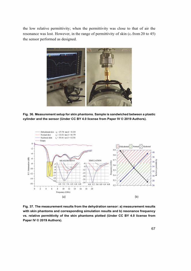
67
the low relative permittivity; when the permittivity was close to that of air the
resonance was lost. However, in the range of permittivity of skin (εr from 20 to 45)
the sensor performed as designed.
Fig. 36. Measurement setup for skin phantoms. Sample is sandwiched between a plastic
cylinder and the sensor (Under CC BY 4.0 license from Paper IV © 2019 Authors).
Fig. 37. The measurement results from the dehydration sensor: a) measurement results
with skin phantoms and corresponding simulation results and b) resonance frequency
vs. relative permittivity of the skin phantoms plotted (Under CC BY 4.0 license from
Paper IV © 2019 Authors).

68
Fig. 38. Sensor response to the drying polyester tissue as function of time. The
resonance is lost after approximately 22 h (Under CC BY 4.0 license from Paper IV ©
2019 Authors).

69
5 Discussion
The first package presented in Paper I was based on a flip-chip technique having
40 pads, all of which needed to be connected to the conductors on the substrate, thus
posing difficulties. This problem was resolved by using conductive and non-
conductive epoxies to provide a barrier between the liquid and the electrical
connections to the chip. Conductive epoxy was placed on the substrate with a
tailored alumina stamp. Moreover, a version where the microfluidic channels were
integrated into the package was demonstrated. The 2nd generation chip in Paper II
had fewer contact pads and the packaging process was changed to take advantage
of thermocompression bonding. This also enabled mass production and fewer
processing steps were needed. Comparing this to wire bond style packages [31],
[32], [63]. The benefits of flip-chip bonding are clear as there is no need for special
techniques to protect the active area of the chip during covering of the wires. The
same feature exists in chip-in-hole style packages [30], [33]. Chip-in-hole derives
some benefits from the relatively flat surface where the microfluidics can be
integrated. However, in the LTCC based package, presented in this work, the
microfluidic channels can be directly manufactured on the package.
In Paper III a resonator with 3 resonating modes at frequencies between 0.7–6
GHz was simulated, manufactured and tested. The system was designed for easy
use with an integrated pumping system. This type of sensor could be suitable to
measure different types of body liquids such as blood, sweat, urine or cerebrospinal
fluid (CSF), which can give indications of certain diseases or problems in humans.
For example, if blood is detected in the CSF it suggests the possibility of a major
health issue. The device was manufactured from printed circuit board, which has
renowned mass production capabilities, and PDMS which is known as a good
material in prototyping or microfluidics and sensor demonstrations. In final tests
with the saline water the sensor showed correspondence of the attenuation of the
1st resonance and amount of saline.
The size of the dehydration sensor, presented in Paper IV, was small (area in
contact with skin 6.4×6.4 mm2) compared to the work presented by other
researchers [56], [64]–[67]. In spite of this small size it yielded clear results from
which distinctions between hydration states in skin phantoms could easily be made.
In the future, the structure could be integrated to a sports watch type of application.
However, before moving to human experiments the vector network analyzer (VNA)
needs to be miniaturized and integrated in conjunction with the sensor. This could
be engineered to generate a signal in a suitable frequency band measuring reflected

70
power. This could be achieved by a voltage-controlled oscillator (VCO) and the
reflected power may be determined using off-the-shelf components.

71
6 Summary and outlook
In this thesis biosensors have been the focus, especially microwave sensors. Two
types of packages for CMOS-based cell culture biosensors were developed where
packages based on LTCC material were proven to be well suited for small sized
CMOS biosensors. The materials and electromagnetic theory behind the response
of the sensors were discussed. Secondly, a sensor for salinity measurement,
including a sample pumping system, was designed and manufactured. Thirdly, a
microwave sensor for real-time dehydration measurement of the skin was
developed.
CMOS based sensor chips are well suited for mass production and enable the
integration of a microprocessor and electronics to drive the sensor elements.
However, these sensor elements need to be in contact with the biological materials
under measurement while the chip size is small. Thus, the packaging is challenging
due to the need for the electrical contacts to be covered, and the materials should
also be biocompatible. LTCC technology was proven to be suitable for the
packaging of these CMOS based biosensors.
Electrical connections to the substrate was made by conductive adhesive which
was stamped onto the substrate. Since the contact pads of the chip were oxidized,
the pads on the chip were gold bumped to achieve a lower resistance and better
reliability of the connection. The chip was bonded to the substrate and the adhesive
was cured. An epoxy underfill was used to seal the gap between the chip and the
substrate. A well for the cell culture made from polypropylene was glued on top of
the package.
Due to the flexibility of the LTCC process these ceramic packages can be easily
customised for different purposes. For example, a small sized package for normal
usage and a larger one, enabling simultaneous optical measurements and
observations by microscope, was demonstrated. Packages proposed in this thesis
have been used on several occasions in the USA and Sweden [68], [69] for cell
experiments, hence proving their durability. In the future, the LTCC technique could
be used to realise a standalone system for cell culture measurement with heaters,
temperature and pH sensors to control the environment for incubation in the
package. Such a package would allow sterilization of the sensor with chemicals
(ethanol) or a heat/steam-based technique. This would enable sensor reusability,
thus reducing the overall cost. The greatest disadvantage of the LTCC package is
the opaque nature of its material but this can be solved by integrating transparent
materials to the package (e.g. plastic or glass lids [70]). However, if the sensor is

72
well characterized, optical inspection is not needed, and the system could be used
for example for drug screening. Data about cell viability would be gathered
automatically without human intervention, thus decreasing the cost of the screening
and enabling continuous monitoring instead of only end-point inspection.
All biological materials have different dielectric properties making microwave
sensors a powerful instrument for monitoring biological activity. By measuring
NaCl (ion) concentration from blood, hydration balance could be determined.
Microfluidics allow the use of samples with a small volume and a microwave sensor
with multiple resonances for monitoring the sample. The resonator developed in
this work was based on interdigitated finger electrodes and sufficient electrical
loading of the medium under measurement. The NaCl concentration (osmolality)
in the medium (water) could be determined. The loss tangent measured by the
microwave-microfluidic sensor was shown to correlate with the concentration of
NaCl in water around the 1 GHz measurement frequency. Groundwork for
developing this type of sensor was established including a manufacturing process
and sample handling with an integrated pumping system. In the future, further tests
with blood should be carried out in order to take other elements into account and to
determine if osmolality can be measured selectively.
To monitor dehydration in vivo, a micromachined split ring resonator was
manufactured and tested in the laboratory using tailored skin phantoms. The design
was based on CSRR and it was optimized using electromagnetic simulation. The
sensor itself worked and showed clear resonance frequency shift when the hydration
state was changing. The results show the feasibility of this sensor for detection of
the moisture level in the skin, but practical use requires further studies and
development. If successful the sensor could provide great advantages in the
monitoring of human activity and dehydration, similar to the heart rate monitoring
which is nowadays a standard procedure.

73
List of references
[1] L. C. Clark, R. Wolf, D. Granger, and Z. Taylor, “Continuous recording of blood oxygen tensions by polarography.,” J. Appl. Physiol., vol. 6, no. 3, pp. 189–193, 1953.
[2] L. C. Clark and C. Lyons, “Electrode systems for continuous monitoring in cardiovascular surgery,” Ann. N. Y. Acad. Sci., vol. 102, no. 1, pp. 29–45, 1962.
[3] G. G. Guilbault and J. G. Montalvo, “A Urea-Specific Enzyme Electrode,” J. Am. Chem. Soc., vol. 91, no. 8, pp. 2164–2165, 1969.
[4] A. Manz, N. Graber, and H. M. Widmer, “Miniaturized total chemical analysis systems: A novel concept for chemical sensing,” Sensors Actuators B. Chem., vol. 1, pp. 244–248, 1990.
[5] S. C. Terry, J. H. Herman, and J. B. Angell, “A Gas Chromatographic Air Analyzer Fabricated on a Silicon Wafer,” IEEE Trans. Electron Devices, vol. 26, no. 12, pp. 1880–1886, 1979.
[6] E. Verpoorte and N. F. De Rooij, “Microfluidics meets MEMS,” Proceedings of the IEEE, vol. 91, no. 6. pp. 930–953, 2003.
[7] “Global Lab On a Chip Market Size, Share, Trends, COVID-19 Impact & Growth Analysis Report – Segmented By Product Type, Technology & Region (North America, Europe, Asia Pacific, Latin America, Middle East, and Africa) – Industry Forecast (2021 to 2026)," Market Data Forecast, Inc., Hyderabad, India. Accessed: Jun., 5, 2021. [Online]. Available: https://www.marketdataforecast.com/market-reports/lab-on-a-chip-market.
[8] G. Nabovati, E. Ghafar-Zadeh, M. Mirzaei, G. Ayala-Charca, F. Awwad, and M. Sawan, “A new fully differential CMOS capacitance to digital converter for lab-on-chip applications,” IEEE Trans. Biomed. Circuits Syst., vol. 9, no. 3, pp. 353–361, 2015.
[9] S. B. Prakash and P. Abshire, “Tracking cancer cell proliferation on a CMOS capacitance sensor chip,” Biosens. Bioelectron., vol. 23, no. 10, pp. 1449–1457, 2008.
[10] N. Couniot, L. A. Francis, and D. Flandre, “A 16 ?? 16 CMOS Capacitive Biosensor Array Towards Detection of Single Bacterial Cell,” IEEE Trans. Biomed. Circuits Syst., vol. 10, no. 2, pp. 364–374, 2016.
[11] C. Xiao and J. H. T. Luong, “On-line monitoring of cell growth and cytotoxicity using electric cell-substrate impedance sensing (ECIS),” Biotechnol. Prog., vol. 19, no. 3, pp. 1000–1005, 2003.
[12] J. C. Chien and A. M. Niknejad, “Oscillator-Based Reactance Sensors With Injection Locking for High-Throughput Flow Cytometry Using Microwave Dielectric Spectroscopy,” IEEE J. Solid-State Circuits, vol. 51, no. 2, pp. 457–472, 2016.
[13] N. Couniot, D. Bol, O. Poncelet, L. A. Francis, and D. Flandre, “A capacitance-to-frequency converter with on-chip passivated

74
microelectrodes for bacteria detection in saline buffers up to 575 MHz,” IEEE Trans. Circuits Syst. II Express Briefs, vol. 62, no. 2, pp. 159–163, 2015.
[14] J. C. Chien, A. Ameri, E. C. Yeh, A. N. Killilea, M. Anwar, and A. M. Niknejad, “A high-throughput flow cytometry-on-a-CMOS platform for single-cell dielectric spectroscopy at microwave frequencies,” Lab Chip, vol. 18, no. 14, pp. 2065–2076, 2018.
[15] T. Mitsunaka et al., “CMOS Biosensor IC Focusing on Dielectric Relaxations of Biological Water with 120 and 60 GHz Oscillator Arrays,” IEEE J. Solid-State Circuits, vol. 51, no. 11, pp. 2534–2543, 2016.
[16] H. Wang, A. Mahdavi, D. A. Tirrell, and A. Hajimiri, “A magnetic cell-based sensor,” Lab Chip, vol. 12, no. 21, p. 4465, 2012.
[17] J. N. Lee, C. Park, and G. M. Whitesides, “Solvent Compatibility of Poly(dimethylsiloxane)-Based Microfluidic Devices,” Anal. Chem., vol. 75, no. 23, pp. 6544–6554, 2003.
[18] P. Karásek, J. Grym, M. Roth, J. Planeta, and F. Foret, “Etching of glass microchips with supercritical water,” Lab Chip, vol. 15, no. 1, pp. 311–318, 2015.
[19] C. E. Hoyle and C. N. Bowman, “Thiol-ene click chemistry,” Angewandte Chemie - International Edition, vol. 49, no. 9, pp.1540-1573, 2010.
[20] B. K. Gale et al., “A review of current methods in microfluidic device fabrication and future commercialization prospects,” Inventions, no. 3, p. 60, 2018.
[21] Y. Imanaka, Multilayered low temperature cofired ceramics (LTCC) technology. New York, NY, USA: Springer, 2005.
[22] M. Sobocinski, J. Putaala, and H. Jantunen, “Multilayer low-temperature co-fired ceramic systems incorporating a thick-film printing process,” in Printed Films: Materials Science and Applications in Sensors, Electronics and Photonics. Cambridge, UK: Woodhead Publishing Ltd., 2012, pp. 134–164.
[23] M. R. Gongora-Rubio, P. Espinoza-Vallejos, L. Sola-Laguna, and J. J. Santiago-Avilés, “Overview of low temperature co-fired ceramics tape technology for meso-system technology (MsST),” Sensors Actuators A Phys., vol. 89, no. 3, pp. 222–241, Apr. 2001.
[24] K. A. Peterson et al., “Novel Microsystem Applications with New Techniques in Low-Temperature Co-Fired Ceramics,” Int. J. Appl. Ceram. Technol., vol. 2, no. 5, pp. 345–363, Sep. 2005.
[25] M. Sobocinski, J. Juuti, H. Jantunen, and L. Golonka, “Piezoelectric unimorph valve assembled on an LTCC substrate,” Sensors Actuators, A Phys., vol. 149, no. 2, pp. 315–319, Feb. 2009.
[26] T. Reinecke et al., “Continuous noninvasive monitoring of cell growth in disposable bioreactors,” Sensors Actuators, B Chem., vol. 251, pp. 1009–1017, 2017.

75
[27] H. Bartsch, T. Welker, K. Welker, H. Witte, and J. Müller, “LTCC based bioreactors for cell cultivation,” IOP Conf. Ser. Mater. Sci. Eng., vol. 104, p. 012001, 2016.
[28] H. B. De Torres, C. Rensch, M. Fischer, A. Schober, M. Hoffmann, and J. Müller, “Thick film flow sensor for biological microsystems,” Sensors Actuators, A Phys., vol. 160, no. 1–2, pp. 109–115, 2010.
[29] H. Bartsch et al., “Surface properties and biocompatibility of thick film materials used in ceramic bioreactors,” Materialia, vol. 5, no. 100213, 2019.
[30] T. Datta-Chaudhuri, P. Abshire, and E. Smela, “Packaging commercial CMOS chips for lab on a chip integration.,” Lab Chip, vol. 14, no. 10, pp. 1753–66, 2014.
[31] H. Wang, A. Mahdavi, D. A. Tirrell, and A. Hajimiri, “A magnetic cell-based sensor,” Lab Chip, vol. 12, no. 21, pp. 4465–4471, 2012.
[32] Lin Li and A. J. Mason, “Post-CMOS parylene packaging for on-chip biosensor arrays,” in 2010 IEEE Sensors, 2010, pp. 1613–1616.
[33] S. Lu, B. Senevirathna, M. Dandin, E. Smela, and P. Abshire, “System Integration of IC chips for Lab-on-CMOS Applications,” in 2018 IEEE International Symposium on Circuits and Systems (ISCAS), 2018, vol. 2018-May, pp. 1–5.
[34] R. Huys et al., “Single-cell recording and stimulation with a 16k micro-nail electrode array integrated on a 0.18 μm CMOS chip,” Lab Chip, vol. 12, no. 7, p. 1274, 2012.
[35] A. Wu, L. Wang, E. Jensen, R. Mathies, and B. Boser, “Modular integration of electronics and microfluidic systems using flexible printed circuit boards.,” Lab Chip, vol. 10, no. 4, pp. 519–521, 2010.
[36] B. Zhang, Q. Dong, C. E. Korman, Z. Li, and M. E. Zaghloul, “Flexible packaging of solid-state integrated circuit chips with elastomeric microfluidics,” Sci. Rep., vol. 3, no. 1, p. 1098, Dec. 2013.
[37] N. Halonen et al., “Low temperature co-fired ceramic package for lab-on-CMOS applied in cell viability monitoring,” Procedia Eng., vol. 120, pp. 1079–1082, 2015.
[38] A. R. von Hippel, Ed., Dielectric materials and applications. Cambridge, MA, USA: The MIT Press, 1952.
[39] E. Nyfors, “Industrial Microwave Sensors---A Review,” Subsurf. Sens. Technol. Appl., vol. 1, no. 1, pp. 23–43, 2000.
[40] P. Jakkula and E. Tahkola, “Microwave Sensor System for the Consistency Measurement in the Pulp and Paper Industry,” Sensors Updat., vol. 7, no. 1, pp. 211–232, Jan. 2000.
[41] S. Kim et al., “Noninvasive in vitro measurement of pig-blood d-glucose by using a microwave cavity sensor,” Diabetes Res. Clin. Pract., vol. 96, no. 3, pp. 379–384, 2012.
[42] F. I. Jamal et al., “Low-Power Miniature K -Band Sensors for Dielectric Characterization of Biomaterials,” IEEE Trans. Microw. Theory Tech., vol.

76
65, no. 3, pp. 1012–1023, 2017. [43] A. Salim, S. H. Kim, J. Y. Park, and S. Lim, “Microfluidic Biosensor Based
on Microwave Substrate-Integrated Waveguide Cavity Resonator,” J. Sensors, vol. 2018, p. 1324145, 2018..
[44] F. I. Jamal, S. Guha, M. H. Eissa, S. Vehring, D. Kissinger, and C. Meliani, “K-Band BiCMOS based near-field biomedical dielectric sensor for Detection of fat and calcium in blood,” in 2015 European Microwave Conference (EuMC), 2015, pp. 821–824..
[45] J. C. Booth, N. D. Orloff, J. Mateu, M. Janezic, M. Rinehart, and J. A. Beall, “Quantitative permittivity measurements of nanoliter Liquid volumes in microfluidic channels to 40 GHz,” IEEE Trans. Instrum. Meas., vol. 59, no. 12, pp. 3279–3288, 2010.
[46] X. Bao et al., “A Planar One-Port Microwave Microfluidic Sensor for Microliter Liquids Characterization,” IEEE J. Electromagn. RF Microw. Med. Biol., vol. 2, no. 1, pp. 10–17, Mar. 2018.
[47] A. Salim and S. Lim, “TM02quarter-mode substrate-integrated waveguide resonator for dual detection of chemicals,” Sensors (Switzerland), no. 6, pp. 1964, 2018.
[48] M. T. Jilnai, W. P. Wen, L. Y. Cheong, and M. Z. U. Rehman, “A microwave ring-resonator sensor for non-invasive assessment of meat aging,” Sensors (Switzerland), vol. 16, no. 1, pp. 52 2016.
[49] R. L. Shao, Y. J. Zhou, and L. Yang, “Quarter-mode spoof plasmonic resonator for a microfluidic chemical sensor,” Appl. Opt., vol. 57, no. 28, p. 8472, Oct. 2018.
[50] G. Yesiloz, M. S. Boybay, and C. L. Ren, “Label-free high-throughput detection and content sensing of individual droplets in microfluidic systems,” Lab Chip, vol. 15, no. 20, pp. 4008–4019, 2015.
[51] B. M. Popkin, K. E. D’Anci, and I. H. Rosenberg, “Water, hydration, and health,” Nutr. Rev., vol. 68, no. 8, pp. 439–458, Aug. 2010.
[52] J. H. Ahn et al., “Meningeal lymphatic vessels at the skull base drain cerebrospinal fluid,” Nature, vol. 572, no. 7767, pp. 62–66, 2019.
[53] J. Hakala, J. Kilpijarvi, M. Sarestoniemi, M. Hamalainen, S. Myllymaki, and T. Myllyla, “Microwave Sensing of Brain Water – a Simulation and Experimental Study Using Human Brain Models,” IEEE Access, vol. 8, pp. 111303–111315, 2020.
[54] M. Tanaka and M. Sato, “Microwave heating of water, ice, and saline solution: Molecular dynamics study,” J. Chem. Phys., vol. 126, no. 3, p. 034509, 2007.
[55] P. Hasgall et al., “IT’IS Database for thermal and electromagnetic parameters of biological tissues, Version 4.0,” IT’IS, 2018. [Online]. Available: https://www.itis.ethz.ch/virtual-population/tissue-properties/database/database-summary/.
[56] F. Trenz, V. Kalpen, R. Weigel and D. Kissinger, "Modeling and

77
measurement of a tissue-equivalent liquid for noninvasive dehydration sensing in the 2.45 GHz ISM-band," 2015 IEEE MTT-S International Microwave Workshop Series on RF and Wireless Technologies for Biomedical and Healthcare Applications (IMWS-BIO), pp. 32-33, 2015.
[57] J. Garrett and E. Fear, "Stable and Flexible Materials to Mimic the Dielectric Properties of Human Soft Tissues," IEEE Antennas and Wireless Propagation Letters, vol. 13, pp. 599-602, 2014.
[58] E. Nyfors and P. Vainikainen, Industrial microwave sensors. Norwood, MA, USA: Artech House, 1989.
[59] S. B. Prakash and P. Abshire, “A fully differential rail-to-rail CMOS capacitance sensor with floating-gate trimming for mismatch compensation,” IEEE Transactions on Circuits and Systems I: Regular Papers, vol. 56, no. 5, pp. 975–986, May 2009.
[60] A. Bogner, C. Steiner, S. Walter, J. Kita, G. Hagen, and R. Moos, “Planar microstrip ring resonators for microwave-based gas sensing: Design aspects and initial transducers for humidity and ammonia sensing,” Sensors (Switzerland), vol. 17, no. 10, p. 2422, 2017.
[61] A. Salim and S. Lim, “Complementary split-ring resonator-loaded microfluidic ethanol chemical sensor,” Sensors (Switzerland), vol. 16, no. 11, pp. 1802, 2016.
[62] S. R. M. Shah et al., “Penetration Depth Evaluation of Split Ring Resonator sensor using In-Vivo Microwave Reflectivity and Ultrasound Measurements,” in 12th European Conference on Antennas and Propagation (EuCAP 2018), 2018.
[63] N. Couniot, D. Bol, O. Poncelet, L. A. Francis, and D. Flandre, “A Capacitance-to-Frequency Converter With On-Chip Passivated Microelectrodes for Bacteria Detection in Saline Buffers Up to 575 MHz,” IEEE Trans. Circuits Syst. II Express Briefs, vol. 62, no. 2, pp. 159–163, Feb. 2015.
[64] I. Butterworth, J. Serallés, C. S. Mendoza, L. Giancardo, and L. Daniel, “A wearable physiological hydration monitoring wristband through multi-path non-contact dielectric spectroscopy in the microwave range,” IEEE MTT-S Int. Microw. Symp. Dig., Sep. pp. 60—61, 2015.
[65] J. Wang, Z. Zilic, and Y. Shu, “Evaluation of an RF wearable device for non-invasive real-time hydration monitoring,” in Proc. IEEE 14th Int. Conf. Wearable Implant. Body Sensor Netw. (BSN), pp. 91—94, May 2017.
[66] M. A. Ionescu and H. Guerin, “System for the remote monitoring of the hydration status of a living being,” U.S. Patent 2016/0058364 A1, Mar. 3, 2016.
[67] A. R. Brendtke, M. Wiehl, F. Groeber, T. Schwarz, H. Walles, and J. Hansmann, “Feasibility study on a microwave-based sensor for mea- suring hydration level using human skin models,” PLoS ONE, vol. 11, no. 4, Apr. 2016, Art. no. e0153145.

78
[68] B. Senevirathna, S. Lu, E. Smela, and P. Abshire, “An imaging platform for real-Time in vitro microscopic imaging for lab-on-cmos systems,” in BioCAS 2019 - Biomedical Circuits and Systems Conference, Proceedings, pp. 1–4, 2019.
[69] K. Bunnfors et al., “Nanoparticle activated neutrophils-on-a-chip: A label-free capacitive sensor to monitor cells at work,” Sensors Actuators B Chem., vol. 313, p. 128020, Jun. 2020.
[70] P. Bembnowicz and L. J. Golonka, “Integration of Transparent Glass Window with LTCC Technology for μTAS Application,” J. Eur. Ceram. Soc. vol. 30, p. 743–749, Feb. 2010.

79
Original publications
I Halonen, N., Kilpijärvi, J., Sobocinski, M., Datta-Chaudhuri, T., Hassinen, A., Prakash, S. B., Möller, P., Abshire, P., Kellokumpu, S., & Lloyd Spetz, A. (2016). Low temperature co-fired ceramic packaging of CMOS capacitive sensor chip towards cell viability monitoring. Beilstein Journal of Nanotechnology, 7, 1871–1877. https://doi.org/10.3762/bjnano.7.179
II Kilpijärvi, J., Halonen, N., Sobocinski, M., Hassinen, A., Senevirathna, B., Uvdal, K., Abshire, P., Smela, E., Kellokumpu, S., Juuti, J., & Lloyd Spetz, A. (2018). LTCC packaged ring oscillator based sensor for evaluation of cell proliferation. Sensors, 18(10), 3346. https://doi.org/10.3390/s18103346
III Kilpijärvi, J., Halonen, N., Juuti, J., & Hannu, J. (2019). Microfluidic microwave sensor for detecting saline in biological range. Sensors, 19(4), 819. https://doi.org/10.3390/s19040819
IV Kilpijärvi, J., Tolvanen, J., Juuti, J., Halonen, N., & Hannu J. (2020). A non-invasive method for hydration status measurement with a microwave sensor using skin phantoms. IEEE Sensors Journal, 20(2), 1095–1104. https://doi.org/10.1109/JSEN.2019.2945817
Reprinted under Creative Commons CC BY 4.0 license1(Papers I–IV © 2016, 2018,
2019 Authors).
Original publications are not included in the electronic version of the dissertation.
1 https://creativecommons.org/licenses/by/4.0/

80

A C T A U N I V E R S I T A T I S O U L U E N S I S
Book orders:Virtual book store
http://verkkokauppa.juvenesprint.fi
S E R I E S C T E C H N I C A
781. Asgharimoghaddam, Hossein (2021) Resource management in large-scale wirelessnetworks via random matrix methods
782. Kekkonen, Jere (2021) Performance of a 16×256 time-resolved CMOS single-photon avalanche diode line sensor in Raman spectroscopy applications
783. Borovkova, Mariia (2021) Polarization and terahertz imaging for functionalcharacterization of biological tissues
784. de Castro Tomé, Mauricio (2021) Advanced electricity metering based on event-driven approaches
785. Järvenpää, Esko (2021) Yläpuolisen siltakaaren optimaalinen muoto
786. Lindholm, Maria (2021) Insights into undesired load factors at work now andtomorrow : findings from different professions and working conditions
787. Miettinen, Jyrki & Visuri, Ville-Valtteri & Fabritius, Timo (2021) Carbon-containingthermodynamic descriptions of the Fe–Cr–Cu–Mo–Ni–C system for modelingthe solidification of steels
788. Tavakolian, Mohammad (2021) Efficient spatiotemporal representation learningfor pain intensity estimation from facial expressions
789. Longi, Henna (2021) Regional innovation systems and company engagement in theArctic context
790. Moltafet, Mohammad (2021) Information freshness in wireless networks
791. Nevanperä, Tuomas (2021) Catalytic oxidation of harmful chlorine- and sulphur-containing VOC emissions : a study of supported Au, Pt and Cu catalysts
792. Baharmast, Aram (2021) Wide dynamic range CMOS receiver techniques for apulsed Time-of-Flight laser rangefinder
793. Haiko, Oskari (2021) Effect of microstructural characteristics and mechanicalproperties on the impact-abrasive and abrasive wear resistance of ultra-highstrength steels
794. Oppenlaender, Jonas (2021) Crowdsourcing creative work
795. Kimbi Yaah, Velma Beri (2021) Development of novel biomass-based materialsfor the treatment of emerging contaminants in water
796. Liu, Chen-Feng (2021) Resource allocation for ultra-reliable and low-latency 5Gcommunication
C797etukansi.fm Page 2 Tuesday, August 17, 2021 1:51 PM

UNIVERSITY OF OULU P .O. Box 8000 F I -90014 UNIVERSITY OF OULU FINLAND
A C T A U N I V E R S I T A T I S O U L U E N S I S
University Lecturer Tuomo Glumoff
University Lecturer Santeri Palviainen
Postdoctoral researcher Jani Peräntie
University Lecturer Anne Tuomisto
University Lecturer Veli-Matti Ulvinen
Planning Director Pertti Tikkanen
Professor Jari Juga
Associate Professor (tenure) Anu Soikkeli
University Lecturer Santeri Palviainen
Publications Editor Kirsti Nurkkala
ISBN 978-952-62-3033-7 (Paperback)ISBN 978-952-62-3034-4 (PDF)ISSN 0355-3213 (Print)ISSN 1796-2226 (Online)
U N I V E R S I TAT I S O U L U E N S I SACTAC
TECHNICA
U N I V E R S I TAT I S O U L U E N S I SACTAC
TECHNICA
OULU 2021
C 797
Joni Kilpijärvi
RF-MICROWAVE SENSOR DEVELOPMENT FOR CELL AND HUMAN IN VITRO AND EX VIVO MONITORING
UNIVERSITY OF OULU GRADUATE SCHOOL;UNIVERSITY OF OULU,FACULTY OF INFORMATION TECHNOLOGY AND ELECTRICAL ENGINEERING;LINKÖPING UNIVERSITY,DEPARTMENT OF PHYSICS, CHEMISTRY AND BIOLOGY (IFM);INFOTECH
C 797
AC
TAJoni K
ilpijärvi
C797etukansi.fm Page 1 Tuesday, August 17, 2021 1:51 PM