
The Hope Project – A paradigm of successful Balkan Integration Katerina Papakonstantinou

c© 2012 Alexandros Papakonstantinou
HIGH-LEVEL AUTOMATION OF CUSTOM HARDWARE DESIGN FORHIGH-PERFORMANCE COMPUTING
BY
ALEXANDROS PAPAKONSTANTINOU
DISSERTATION
Submitted in partial fulfillment of the requirementsfor the degree of Doctor of Philosophy in Electrical and Computer Engineering
in the Graduate College of theUniversity of Illinois at Urbana-Champaign, 2012
Urbana, Illinois
Doctoral Committee:
Associate Professor Deming Chen, ChairProfessor Jason Cong, UCLAProfessor Wen-Mei HwuProfessor Martin Wong
ABSTRACT
This dissertation focuses on efficient generation of custom processors from
high-level language descriptions. Our work exploits compiler-based optimiza-
tions and transformations in tandem with high-level synthesis (HLS) to build
high-performance custom processors. The goal is to offer a common multi-
platform high-abstraction programming interface for heterogeneous compute
systems where the benefits of custom reconfigurable (or fixed) processors can
be exploited by the application developers.
The research presented in this dissertation supports the following thesis: In
an increasingly heterogeneous compute environment it is important to lever-
age the compute capabilities of each heterogeneous processor efficiently. In
the case of FPGA and ASIC accelerators this can be achieved through HLS-
based flows that (i) extract parallelism at coarser than basic block gran-
ularities, (ii) leverage common high-level parallel programming languages,
and (iii) employ high-level source-to-source transformations to generate high-
throughput custom processors.
First, we propose a novel HLS flow that extracts instruction level par-
allelism beyond the boundary of basic blocks from C code. Subsequently,
we describe FCUDA, an HLS-based framework for mapping fine-grained and
coarse-grained parallelism from parallel CUDA kernels onto spatial paral-
lelism. FCUDA provides a common programming model for acceleration
on heterogeneous devices (i.e. GPUs and FPGAs). Moreover, the FCUDA
framework balances multilevel granularity parallelism synthesis using effi-
cient techniques that leverage fast and accurate estimation models (i.e. do
not rely on lengthy physical implementation tools). Finally, we describe an
advanced source-to-source transformation framework for throughput-driven
parallelism synthesis (TDPS), which appropriately restructures CUDA ker-
nel code to maximize throughput on FPGA devices. We have integrated the
TDPS framework into the FCUDA flow to enable automatic performance
ii

porting of CUDA kernels designed for the GPU architecture onto the FPGA
architecture.
iii

I dedicate this dissertation to my wife, my parents, and my sister for their
immeasurable love and support throughout my graduate studies.
iv
ACKNOWLEDGMENTS
This project would have not been possible without the support of many
people. I thank my advisor Deming Chen and my coadvisor Wen-Mei Hwu for
providing invaluable feedback, guidance and help throughout all the phases
of my PhD work. Sincere thanks go to Jason Cong for supporting my PhD
thesis with tools and constructive criticism. Finally, I would like to thank my
committee member, Martin Wong, for his friendly chats and advice and for
his great lectures during the first course I took at the University of Illinois
in Urbana-Champaign.
I would like to extend a special thanks to all the contributors in the FCUDA
work, staring from Karthik Gururaj who helped me decisively in setting up
the infrastructure for such a complex project. Moreover, I sincerely thank
John Stratton and Eric Liang for coauthoring and codeveloping several of
FCUDA documents and tools.
I am grateful to my fellow labmates at the CADES group, and especially
to Lu Wan, Chen Dong, Scott Kromar, Greg Lucas and Christine Chen
for making the lab a great place to work and collaborate. I should not
omit to extend many thanks to the Impact lab colleagues Chris Rodrigues,
Sara Baghsorkhi, Xiao-Long, Nasser, Ray and Liwen for all the stimulating
discussions and friendly chats during the Impact group meetings.
I am deeply indebted to my parents, Melina and Manolis, for serving as a
constant source of love and unconditional support of my decisions and aca-
demic pursuits. I am grateful to my sister, Ria, for joining me during my
move to the U.S. and helping me to settle down in Champaign, Illinois. Fi-
nally, it would have not been possible to complete this dissertation without
the immeasurable help and loving support of my wife, Eleni; her love, con-
fidence in me and unlimited support have helped me develop into a better
scholar and person.
v
TABLE OF CONTENTS
LIST OF TABLES . . . . . . . . . . . . . . . . . . . . . . . . . . . . . viii
LIST OF FIGURES . . . . . . . . . . . . . . . . . . . . . . . . . . . . ix
LISTINGS . . . . . . . . . . . . . . . . . . . . . . . . . . . . . . . . . . xi
LIST OF ALGORITHMS . . . . . . . . . . . . . . . . . . . . . . . . . xii
LIST OF ABBREVIATIONS . . . . . . . . . . . . . . . . . . . . . . . xiii
CHAPTER 1 INTRODUCTION . . . . . . . . . . . . . . . . . . . . 11.1 Compute Heterogeneity . . . . . . . . . . . . . . . . . . . . . . 21.2 Programming Models and Programmability . . . . . . . . . . 31.3 Reconfigurable Computing . . . . . . . . . . . . . . . . . . . . 5
CHAPTER 2 RELATED WORK . . . . . . . . . . . . . . . . . . . . 9
CHAPTER 3 EPOS APPLICATION ACCELERATOR . . . . . . . . 133.1 EPOS Overview . . . . . . . . . . . . . . . . . . . . . . . . . . 143.2 ILP-Driven Scheduling . . . . . . . . . . . . . . . . . . . . . . 173.3 Forwarding Path Aware Binding . . . . . . . . . . . . . . . . . 193.4 Evaluation . . . . . . . . . . . . . . . . . . . . . . . . . . . . . 30
CHAPTER 4 CUDA TO FPGA SYNTHESIS . . . . . . . . . . . . . 354.1 Overview of Programming Models in FCUDA . . . . . . . . . 364.2 FCUDA Framework . . . . . . . . . . . . . . . . . . . . . . . . 404.3 Transformations and Optimizations in FCUDA Compilation . 484.4 Evaluation . . . . . . . . . . . . . . . . . . . . . . . . . . . . . 55
CHAPTER 5 ML-GPS . . . . . . . . . . . . . . . . . . . . . . . . . . 625.1 Background and Motivation . . . . . . . . . . . . . . . . . . . 635.2 ML-GPS Framework Overview . . . . . . . . . . . . . . . . . . 655.3 Design Space Exploration . . . . . . . . . . . . . . . . . . . . 685.4 Evaluation . . . . . . . . . . . . . . . . . . . . . . . . . . . . . 72
vi
CHAPTER 6 THROUGHPUT-DRIVEN PARALLELISM SYN-THESIS (TDPS) . . . . . . . . . . . . . . . . . . . . . . . . . . . . 786.1 Background and Motivation . . . . . . . . . . . . . . . . . . . 796.2 The TDPS Framework . . . . . . . . . . . . . . . . . . . . . . 856.3 Evaluation . . . . . . . . . . . . . . . . . . . . . . . . . . . . . 104
CHAPTER 7 CONCLUSION . . . . . . . . . . . . . . . . . . . . . . 109
REFERENCES . . . . . . . . . . . . . . . . . . . . . . . . . . . . . . . 112
vii
LIST OF TABLES
3.1 Execution Cycles for Different ILP Schemes . . . . . . . . . . 313.2 Comparison of FWP-Aware Binding Algorithms . . . . . . . . 323.3 NISC vs. EPOS: Cycles . . . . . . . . . . . . . . . . . . . . . 333.4 NISC vs. EPOS: Frequency (MHz) . . . . . . . . . . . . . . . 343.5 NISC vs. EPOS: Total MUX Inputs . . . . . . . . . . . . . . . 34
4.1 FCUDA Pragma Directives . . . . . . . . . . . . . . . . . . . 474.2 CUDA Kernels . . . . . . . . . . . . . . . . . . . . . . . . . . 564.3 maxP Scheme Parameters . . . . . . . . . . . . . . . . . . . . 584.4 maxPxU Scheme Parameters . . . . . . . . . . . . . . . . . . . 584.5 maxPxUxM Scheme Parameters . . . . . . . . . . . . . . . . . 58
viii
LIST OF FIGURES
3.1 High-level synthesis flow . . . . . . . . . . . . . . . . . . . . . 143.2 EPOS architecture . . . . . . . . . . . . . . . . . . . . . . . . 163.3 Binding impact on FWP and MUX count . . . . . . . . . . . 213.4 Building the compatibility graph from the data-dependence
graph . . . . . . . . . . . . . . . . . . . . . . . . . . . . . . . . 243.5 Building the network graph . . . . . . . . . . . . . . . . . . . 253.6 Building the Fschema values . . . . . . . . . . . . . . . . . . . 263.7 Effect of flow on binding feasibility . . . . . . . . . . . . . . . 273.8 Forwarding path rules . . . . . . . . . . . . . . . . . . . . . . 293.9 ILP - Extraction features (SP&HB: superblock & hyper-
block, RFB: register file bypassing, POS: predicated oper-ation speculation) . . . . . . . . . . . . . . . . . . . . . . . . . 31
3.10 EPOS vs. NISC speedup . . . . . . . . . . . . . . . . . . . . . 34
4.1 FCUDA flow . . . . . . . . . . . . . . . . . . . . . . . . . . . 364.2 CUDA programming model . . . . . . . . . . . . . . . . . . . 384.3 Autopilot C programming model . . . . . . . . . . . . . . . . 394.4 Task synchronization schemes . . . . . . . . . . . . . . . . . . 444.5 Two-level task hierarchy in kernels with constant memory . . 494.6 Performance comparison for three parallelism extraction
schemes . . . . . . . . . . . . . . . . . . . . . . . . . . . . . . 594.7 Task synchronization scheme comparison . . . . . . . . . . . . 604.8 FPGA vs. GPU comparison . . . . . . . . . . . . . . . . . . . 61
5.1 Thread, core, core-cluster and memory BW granularities . . . 635.2 Design space of mm kernel . . . . . . . . . . . . . . . . . . . . 655.3 Performance attributes of mm design space configurations . . 665.4 Source code transformations (mm kernel) . . . . . . . . . . . . 665.5 ML-GPS overview . . . . . . . . . . . . . . . . . . . . . . . . . 675.6 Array partition and unroll effects on latency . . . . . . . . . . 715.7 Multigranularity parallelism design spaces . . . . . . . . . . . 745.8 Performance comparison: ML-GPS vs. SL-GPS . . . . . . . . 755.9 Latency comparison: FPGA vs. GPU . . . . . . . . . . . . . . 765.10 Energy comparison: FPGA vs. GPU . . . . . . . . . . . . . . 77
ix
6.1 The TDPS flow integrated in the FCUDA flow . . . . . . . . . 836.2 Hierarchical region graph (HRG) for DWT kernel . . . . . . . 856.3 SNC region motions . . . . . . . . . . . . . . . . . . . . . . . . 896.4 DWT HRG after SNC motions stage . . . . . . . . . . . . . . 926.5 DWT HRG after burst conversion stage . . . . . . . . . . . . . 946.6 Dynamic data coalescing interface of FCUDA core to mem-
ory controller (MC) . . . . . . . . . . . . . . . . . . . . . . . . 946.7 DWT HRG after burst conversion stage . . . . . . . . . . . . . 966.8 DWT HRG after CF normalization . . . . . . . . . . . . . . . 996.9 Interference graphs for graph coloring . . . . . . . . . . . . . . 1036.10 CTA execution speedup by cummulatively adding to op-
timization level, O, SNC region motions (SM), burst con-version (BC), TRN region motions (TM), and control flownormalization (CFN). . . . . . . . . . . . . . . . . . . . . . . . 106
6.11 Effectiveness of TPc metric (left axis shows TPc value, rightaxis shows execution latency) . . . . . . . . . . . . . . . . . . 107
6.12 Kernel execution speedup using TDPS vs. FCUDA . . . . . . 108
x
LISTINGS
4.1 CUDA code for CP kernel . . . . . . . . . . . . . . . . . . . . 424.2 Thread-loop instantiation for CP kernel . . . . . . . . . . . . . 434.3 Threadblock-loop instantiation for CP kernel . . . . . . . . . . 434.4 Transformed CP kernel . . . . . . . . . . . . . . . . . . . . . . 504.5 Data-transfer statement percolation . . . . . . . . . . . . . . . 544.6 Procedural abstraction of tasks . . . . . . . . . . . . . . . . . 556.1 CUDA code for DWT kernel . . . . . . . . . . . . . . . . . . . 816.2 C code for DWT kernel . . . . . . . . . . . . . . . . . . . . . . 826.3 Unnormalize CF containing CMP and TRN regions . . . . . . 976.4 CF normalization using variable privatization . . . . . . . . . 986.5 CF normalization using compute reimplementation . . . . . . 98
xi
LIST OF ALGORITHMS
3.1 Operation Scheduling within each Procedure . . . . . . . . . . 20
3.2 Simple FWP Aware Binding . . . . . . . . . . . . . . . . . . . 22
4.1 FCUDA compilation . . . . . . . . . . . . . . . . . . . . . . . . 46
4.2 Global Memory Accesses Handling . . . . . . . . . . . . . . . . 51
5.1 Binary Search . . . . . . . . . . . . . . . . . . . . . . . . . . . . 73
6.1 Graph coloring of the interference graph . . . . . . . . . . . . . 103
xii
LIST OF ABBREVIATIONS
API Application Programming Interface
ASIC Application Specific Integrated Circuit
BRAM Block RAM
CMP Chip Multiprocessor
CPU Central Processing Unit
CTA Cooperative Thread Array
CC Custom Core
CF Control Flow
DSP Digital Signal Processing
DDR Double Data Rate
EPIC Explicitly Parallel Instruction Computing
EPOS Explicitly Parallel Operations System
ESP Explicit Synchronization Point
FPGA Field Programmable Gate Array
GPU Graphics Processing Unit
HLS High Level Synthesis
HLL High Level Language
HPC High Performance Computing
HRG Hierarchical Region Graph
ILP Instruction Level Parallelism
xiii
ISP Implicit Synchronization Point
MC Memory Controller
ML-GPS Multilevel-Granularity Parallelism Synthesis
rID Region Identifier
RTL Register Transfer Level
SIMD Single Instruction Multiple Data
SoC System on Chip
SiP System in Package
S2C SIMT-to-C
TDPS Throughput-Driven Parallelism Synthesis
tIDX Thread Index
TiVAR Thread-Index Invariant
TVAR Thread-Index Variant
VLIW Very Long Instruction Word
xiv
CHAPTER 1
INTRODUCTION
Parallel processing, once exclusively employed in supercomputing servers and
clusters, has permeated nearly every digital computing domain during the
last decade. Democratization of parallel computing was driven by the power
wall encountered in traditional single-core processors, and it was enabled by
the continued shrinking of transistor feature size that rendered chip multipro-
cessors (CMP) feasible. Meanwhile, the importance of parallel processing in
a growing set of applications that leverage computationally heavy algorithms,
such as simulation, mining or synthesis, underlined the need for on-chip con-
currency at a granularity coarser than instruction level. The vast amounts
of data used in such applications often render processing throughput more
important than processing latency. Massive parallel compute capability is
necessary to satisfy such high throughput requirements.
Achieving higher on-chip concurrency predominantly relies on increasing
the percentage of on-chip silicon real estate devoted to compute modules. In
other words, instantiating more, but simpler (i.e. without complex out of
order and speculative execution engines), cores. This philosophy is reflected
in the architecture of different multicore and manycore devices such as the
Cell-BE [1], the TILE family [2] and the GPU [3, 4] devices. Apart from a
larger number of cores, these devices also employ different memory models
and architectures. The traditional unified memory space model that is im-
plemented with large multilevel caches in traditional processors is replaced
by multiple programmer-visible memory spaces based on distributed on-chip
memories. Moreover, data transfers between off-chip and on-chip memory
spaces are explicitly handled by the programmer.
Achieving high throughput through parallelism extraction at the opera-
tion, the data and the task level has been traditionally accomplished with cus-
tom processors. Application-specific processors have been employed in sys-
tems used in time-sensitive applications with real-time and/or high through-
1
put requirements. Video and audio encoders/decoders, automotive con-
trollers and even older GPUs have been implemented as custom ASIC de-
vices targeted to serve specific application domains. However, skyrocketing
fabrication costs make the use of custom processors impractical in applica-
tions with low-volume deployment. On the other hand, FPGAs have been
growing into viable alternatives for acceleration of compute-intensive appli-
cations with high throughput requirements. By integrating large amounts of
reconfigurable logic along with high-performance hard macros for compute
(e.g. DSPs) and data communication (e.g. PCIe PHY) they are provid-
ing an attractive platform for implementing custom processors that may be
reprogrammed.
1.1 Compute Heterogeneity
Current high-performance computing systems are based on a model that
combines conventional general purpose CPUs for the tasks that are pre-
dominantly sequential (i.e. tasks that contain fine-grained instruction level
parallelism) with throughput-oriented multicore devices that can efficiently
handle massively parallel tasks. This model has also been successfully used
in the supercomputing domain. For example, Roadrunner [5] is based on
AMD Opteron CPUs [6] and IBM Cell [1] multicores and it was the first
supercomputer to break the peta-FLOP barrier. Moreover, Novo-G [7] is a
supercomputer located at the University of Florida comprising 26 Intel Xeon
CPUs [8] and 192 Altera FPGAs [9]. Finally, the Titan supercomputer [10],
which currently holds the leading position in the Top 500 supercomputers
ranking, as well as the Tianhe-1A supercomputer [11], which was one of the
first supercomputers to break the petaflop performance barrier, employ mul-
ticore CPUs (AMD Opteron [6], and Intel Xeon [8], respectively) with Nvidia
Tesla GPUs [4].
The benefits of heterogeneous systems lie in the use of different applica-
tion workloads with different characteristics and throughput requirements
which are better served by different architectures. The promise of hetero-
geneous compute systems is driving industry towards higher integration of
heterogeneity for higher performance and lower power and cost. On-chip in-
tegration has been led in the reconfigurable computing domain with 32-bit
2
PowerPC processors embedded in Xilinx Virtex-2 [12] and subsequent Virtex
and other FPGA devices [13]. Devices integrating conventional CPUs with
graphics controllers [14] or even full-blown GPUs [15] have been recently
released by the major microprocessor vendors, presaging important develop-
ments in the software side as well. The value of heterogeneity is especially
important in the embedded domain where low area and power footprints as
well low cost are critical factors leading to interesting industry collaborations,
such as the forthcoming Stellarton [16] system-in-package (SIP) which pairs
an Intel Atom CPU with an Altera FPGA.
Exploring higher degrees of heterogeneity seems a natural follow-up step.
By “higher degree” we refer to the extension of the basic model to include
more than one type of throughput-oriented device along the conventional
general-purpose CPU. The diverse architectures and features of different ac-
celerators render them optimal for different types of applications and usage
scenarios. For example, Cell [1] is a multiprocessor system-on-chip (MPSoC)
based on a set of heterogeneous cores. Thus, it can operate autonomously,
exploiting both task and data level parallelism, albeit at the cost of lower
on-chip concurrency (i.e. it has fewer cores than other types of multicore
devices). GPUs, on the other hand, consist of hundreds of processing cores
clustered into streaming multiprocessors (SMs) that can handle kernels with
a high degree of data-level parallelism. However, launching execution on the
SMs requires a host processor. An early effort at increased heterogeneity was
the Quadro Plex cluster [17] at the University of Illinois, which comprised 16
nodes that combined AMD Opteron CPUs with Nvidia GPUs and Xilinx FP-
GAs. In a more recent effort, researchers at Imperial College demonstrated
the advantages of utilizing CPUs, GPUs and FPGAs for N-body simulations
on the Axel compute cluster [18].
1.2 Programming Models and Programmability
The advantages of heterogeneity do not come without challenges. One of the
major challenges that has slowed down or even hindered wide adoption of het-
erogeneous systems is programmability. Due to their architecture differences,
throughput-oriented devices have traditionally supported different program-
ming models. Such programming models differ in several ways including
3
the level of abstraction and the structures used to express and map appli-
cation parallelism onto the hardware architecture. Migrating from platform-
independent and well-established general purpose programming models (e.g.
C/C++ and Java) to device-dependent and low-abstraction programming
models involves a steep learning curve with an associated productivity cost.
Moreover, achieving efficient concurrency in several of these programming
models entails partial understanding of the underlying hardware architecture,
thus restricting adoption across a wide range of programmers and scientists.
The evolution in programmability of GPUs, FPGAs and other multicore
devices, such as the Cell MPSoC, reflect the lessons learned by industry and
academia. Issues such as low abstraction (e.g. RT-level programming on
FPGAs) and domain-specific modeling (e.g. OpenGL and DirectX graphics-
oriented programming models on GPUs) have been addressed to enable
higher adoption. The proliferation of high-level synthesis (HLS) tools for FP-
GAs, and the introduction of C-based programming models such as CUDA
for GPUs have contributed significantly toward democratization of parallel
computing. Nevertheless, achieving high-performance in an efficient man-
ner in heterogeneous systems still remains a challenge. The use of different
parallel programming models by heterogeneous accelerators complicates the
efficient utilization of the devices available in heterogeneous compute clus-
ters, which reduces productivity and restricts optimal matching of kernels to
accelerators.
In this dissertation we focus on the programmability of FPGA devices.
In particular we leverage HLS techniques along with compiler techniques to
build frameworks that can help the programmer to efficiently design custom
and domain-specific accelerators on reconfigurable fabric. Our work aims to
enable high design abstraction, promote programming homogeneity within
heterogeneous compute systems and achieve fast performance evaluation of
alternative implementations. In the next sections we motivate the use of
FPGAs as acceleration devices and we discuss our contributions. The tech-
niques implemented in this work can potentially be employed with minor
adjustments for the design of ASIC accelerators. Alternatively, novel com-
mercial tools [19] propose automated conversion of FPGA-based designs into
ASICs.
4
1.3 Reconfigurable Computing
State-of-the-art reconfigurable devices fabricated with the latest process tech-
nologies host a heterogeneous set of hard IPs (e.g. PLLs, ADCs, PCIe PHYs,
CPUs and DSPs) along with millions of reconfigurable logic cells and thou-
sands of distributed static memories (e.g. BRAMs). Their abundant compute
and memory storage capacity makes FPGAs attractive for the acceleration
of compute intensive applications [20, 21, 22], whereas the hard IP modules
offer compute and data communication capacity, enabling high-performance
system-on-chip (SoC) implementations [23]. One of the main benefits of hard-
ware reconfigurability is increased flexibility with regard to leveraging differ-
ent types of application-specific parallelism, e.g. coarse and fine-grained,
data and task-level and versatile pipelining. Moreover, parallelism can be
leveraged across FPGA devices such as in the Convey HC-1 [24] application-
specific instruction processor (ASIP) which combines a conventional multi-
core CPU with FPGA-based custom instruction accelerators. The potential
of multi-FPGA systems to leverage massive parallelism has been also ex-
ploited in the recently launched Novo-G supercomputer [7], which hosts 192
reconfigurable devices.
Power is undeniably becoming the most critical metric of systems in all
application domains from mobile devices to cloud clusters. FPGAs offer a sig-
nificant advantage in power consumption over CPUs and GPUs. J. Williams
et al. [25] showed that the computational density per watt in FPGAs is much
higher than in GPUs. The maximum power consumption of the 192-FPGA
Novo-G [7] is roughly three orders of magnitude lower compared to Opteron-
based Jaguar [26] and Cell-based Roadrunner [5] supercomputers, while deliv-
ering comparable performance for bioinformatics-related applications. Apart
from application customization and low-power computing, FPGAs also offer
long-term reliability (i.e. longer lifetime due to low-temperature operation),
system deployment flexibility (i.e. can be deployed independently as SoC
or within arbitrary heterogeneous compute system) and real-time execution
capabilities. Moreover, they can serve as general purpose, domain-specific or
application-specific processors by combining embedded hard/soft CPUs with
custom reconfigurable logic.
However, hardware design has been traditionally based on RTL languages,
such as VHDL and Verilog. Programming in such low-abstraction languages
5
requires hardware design knowledge and severely limits productivity (com-
pared to higher-level languages used in other throughput-oriented devices).
Similarly to compilers in software design, high-level synthesis (HLS) offers
higher abstraction in hardware design by automating the generation of RTL
descriptions from algorithm descriptions written in traditional high-level pro-
gramming languages (e.g. C/C++). Thus, HLS allows the designer to focus
on the application algorithm rather than on the RTL implementation de-
tails (similarly to how a compiler abstracts away the underlying processor
and its corresponding assembly representation). HLS tools transform an un-
timed high-level specification into a fully timed implementation in three main
steps: (i) hardware resource allocation, (ii) computation scheduling, and (iii)
computation and data binding onto hardware resources [27]. Different ap-
proaches have been proposed over the years for automatically transforming
high-level-language (HLL) descriptions of applications into custom hardware
implementations. The goal of all these efforts is to exploit the spatial paral-
lelism of hardware resources by identifying and extracting parallelism in the
HLL code. Most of these approaches, however, are confined by basic block
level parallelism described within the intermediate CDFG (control-data flow
graphs) representation of the HLL description. In this dissertation we pro-
pose a new high-level synthesis framework which can leverage instruction-
level parallelism (ILP) beyond the boundary of the basic blocks. The pro-
posed framework leverages the parallelism flexibility within superblocks and
hyperblocks formed through advanced compiler techniques [28] to generate
domain-specific processors with highly improved performance. We discuss
our HLS flow, called EPOS, in Chapter 3.
Even though application-specific processors may be deployed as autonomous
SoCs, the performance advantages of FPGA and ASIC-based custom proces-
sors can also be exploited in highly parallel applications or kernels. Thus,
the concept of heterogeneous compute systems that combine ILP-oriented
CPUs (for sequential tasks) and throughput-oriented accelerators (for par-
allel tasks) can be served well by reconfigurable devices. HLS can provide
an efficient path for designing such FPGA/ASIC accelerators. However, the
sequential semantics of traditional programming languages restrict HLS tools
from extracting parallelism at granularities coarser than instruction-level par-
allelism (ILP). We address this by leveraging the CUDA parallel program-
ming model, which was designed for GPU devices, to generate fast custom
6
accelerators on FPGAs. Our CUDA-to-FPGA framework, called FCUDA,
is based on HLS for automatic RTL generation. A source-to-source compi-
lation engine initially transforms the CUDA code into explicitly parallel C
code which is subsequently synthesized by the HLS engine into parallel RTL
designs (Chapter 4). Furthermore, FCUDA enables a common programming
model for heterogeneous systems that contain GPUs and FPGAs.
As mentioned earlier, reconfigurable fabric allows leveraging of application
parallelism across different granularities. Nevertheless, the effect on through-
put depends on the combined effect of different parallelism granularities on
clock frequency and execution cycles. Evaluation of the rich design space
through the full RTL synthesis and physical implementation flow is pro-
hibitive. In other words, raising the programming abstraction with HLS is
not enough to exploit the full potential of reconfigurable devices. In Chapter
5 we extend the FCUDA framework to enable efficient multilevel granularity
parallelism exploration. The proposed techniques leverage (i) resource and
clock period estimation models, (ii) an efficient design space search heuristic,
and (iii) design floorplanning to identify a near-optimal application mapping
onto the reconfigurable logic. We show that by combining HLS with the
proposed design space exploration flow, we can generate high-performance
FPGA accelerators for massively parallel CUDA kernels.
Supporting a homogeneous programming model across heterogeneous com-
pute architectures, as done with FCUDA, facilitates easier functionality port-
ing across heterogeneous architectures. However, it may not exploit the per-
formance potential of the target architecture without device-specific code
tweaking. Performance is affected by the degree of effectiveness in map-
ping computation onto the target architecture. Restructuring the organiza-
tion of computation and applying architecture-specific optimizations may be
necessary to fully take advantage of the performance potential of throughput-
oriented architectures, such as FPGAs. In Chapter 6 we present the throughput-
driven parallelism synthesis (TDPS) framework, which enables automatic
performance porting of CUDA kernels onto FPGAs. In this work we pro-
pose a code optimization framework which analyzes and restructures CUDA
kernels that are optimized for GPU devices in order to facilitate synthesis of
high-throughput custom accelerators on FPGA.
The next chapter presents previous research work on high-level synthe-
sis and throughput-oriented accelerator design. Chapters 3, 4 and 5 discuss
7
our work on EPOS, FCUDA and multilevel granularity parallelism synthesis.
Subsequently, Chapter 6 discusses the automated code restructuring frame-
work we designed, which enables throughput-driven parallelism synthesis for
compilers like FCUDA that target heterogeneous compute arhictectures. Fi-
nally, Chapter 7 concludes this dissertation.
8
CHAPTER 2
RELATED WORK
Ongoing developments in the field of high-level synthesis (HLS) have led to
the emergence of several industry [29, 30, 31] and academia based [32, 33, 34]
tools that can generate device-specific RTL descriptions from popular high-
level programming Languages (HLLs). Such tools help raise the abstrac-
tion of the programming model and constitute a significant improvement
in FPGA usability. However, the sequential semantics of traditional pro-
gramming languages greatly inhibit HLS tools from extracting parallelism at
coarser granularities than instruction-level parallelism (ILP). Even though
parallelizing optimizations such as loop unrolling may help extract coarser-
granularity parallelism at the loop level [35, 36], the rich spatial hardware
parallelism of FPGAs may not be optimally utilized, resulting in suboptimal
performance.
The EPOS flow has several features in common with the NISC work pro-
posed by M. Reshadi et al. [34]. This custom processor architecture removes
the abstraction of the instruction set and compiles HLL applications directly
onto a customizable datapath which is controlled by either memory-stored
control words or traditional FSM logic. The compilation of the NISC sys-
tem is based on a concurrent scheduling and binding scheme on basic blocks.
Our processor architecture, EPOS, builds on this instruction-less architec-
ture by adding new architectural elements and employing novel scheduling
and binding schemes for exploiting instruction-level parallelism beyond basic
blocks.
The increasingly significant effect of long interconnects on power, timing
and area has led to the development of interconnect-driven HLS techniques.
J. Cong et al. [37] have looked into the interconnect-aware binding of a sched-
uled DFG on a distributed register file microarchitecture (DRFM). Based on
the same DRFM architecture, K. Lim et al. [38] have proposed a complete
scheduling and binding solution which considers minimization of intercon-
9
nections between register files and FUs. EPOS, on the other hand, uses a
unified register-file (RF) and allows results to be forwarded directly from the
producing to the consuming FUs for reduced latency.
J. Babb et al. [39] focused on extracting parallelism by splitting an appli-
cation into tiles of computation and data storage with inter-tile communica-
tions based on virtual wires. Virtual wires comprise the pipelined connections
between endpoints of a wire connecting two tiles. Application data is dis-
tributed into small tile memory blocks and computation is then assigned to
the different tiles. This work can produce efficient parallel processing units
for the class of applications that can be efficiently distributed into equal data
and computation chunks. However, applications with control-intensive algo-
rithms could result in contention on the communication through the virtual
wires, imposing many idle cycles on the distributed datapaths. We leverage
a similar tiling approach in FCUDA, but only at the level of core-clusters.
In a different approach, S. Gupta [40, 41] has focused on extracting par-
allelism by performing different types of code motions and compiler opti-
mizations in the CDFG of the program. In particular, they maintain a
hierarchical-task-graph (HTG) besides the traditional CDFG. The nodes in
an HTG represent HLL control-flow constructs, such as loops and if-then-else
constructs. The authors show that their tool, named SPARK, offers signifi-
cant reductions both in the number of controller states and also in the latency
of the application. However, all the code motions are validated using CDFGs
built from basic blocks, which may limit the opportunity for optimizations.
In FCUDA we employ similar code motion optimizations, but at the task
level (instead of instruction level). Moreover, the TDPS framework (Chap-
ter 6) integrated in FCUDA, leverages hierarchical region graphs to represent
control flow structures in the code and facilitate throughput-oriented code
restructuring.
The shift toward parallel computing has resulted in a growing interest in
computing systems with heterogeneous processing modules (e.g. multicore
CPUs, manycore GPUs or arrays of reconfigurable logic blocks in FPGAs).
As a consequence, several new programming models [42, 43, 44] that explic-
itly expose coarse-grained parallelism have been proposed. An important
requirement with respect to the usability of these systems is the support of a
homogeneous programming interface. Recent works have leveraged parallel
programming models in tandem with high-level synthesis (HLS) to facilitate
10
high abstraction parallel programming of FPGAs using parallel programming
models [45, 46, 47, 48].
The popularity of C across different compute systems makes this program-
ming model a natural choice for providing a single programming interface
across different compute platforms such as FPGAs and GPUs. Diniz et al.
[33] propose a HLS flow which takes C code as input and outputs RTL code
that exposes loop iteration parallelism. Baskaran et al. [49] leverage the
polyhedral model to convert parallelism in C loop nests into multithreaded
CUDA kernels. Their framework also identifies off-chip memory data blocks
with high reuse and generates data transfers to move data to faster on-chip
memories.
The OpenMP programming interface is a parallel programming model that
is widely used in conventional multicore processors with shared memory
spaces. The transformation framework in [46] describes how the different
OpenMP pragmas are interpreted during VHDL generation, but it does not
deal with memory space mapping. On the other hand, the OpenMP-to-
CUDA framework proposed in [50] transforms the directive-annotated paral-
lelism into parallel multi-threaded kernels, in addition to providing memory
space transformations and optimizations to support the migration from a
shared memory space (in OpenMP) to a multi-memory space architecture
(in CUDA). The OpenMP programming model is also used in the optimizing
compiler of the Cell processor [51] to provide a homogeneous programming
interface to the processor’s PPE and SPE cores while supporting a single
memory space abstraction. As described in [51], the compiler can orches-
trate DMA transfers between the different memory spaces, while a compiler-
controlled cache scheme takes advantage of temporal and spatial data access
locality.
Exploration of several configurations in the hardware design space is often
restricted by the slow synthesis and place-and-route (P&R) processes. HLS
tools have been used for evaluating different design points in previous work
[35, 36]. Execution cycles and area estimates from HLS were acquired without
going through logic synthesis of the RTL. Array partitioning was exploited
together with loop unrolling to improve compute parallelism and eliminate
array access bottlenecks. Given an unroll factor, all the nondependent array
accesses were partitioned. However. such an aggressive partitioning strat-
egy may severely impact the clock period (i.e. array partitioning results in
11

extra address/data busses, address decoding and routing logic for on-chip
memories). In this work, we identify the best array partition degree con-
sidering both kernel and device characteristics through resource and clock
period estimation models.
12
CHAPTER 3
EPOS APPLICATION ACCELERATOR
Different approaches have been proposed over the years for automatically
transforming high-level-language (HLL) descriptions of applications into cus-
tom hardware implementations. Most of these approaches, however are con-
fined by basic block level parallelism described within the CDFGs (control-
data flow graphs). In this chapter we present a high-level synthesis flow which
can leverage instruction-level parallelism (ILP) beyond the boundary of the
basic blocks. We extract statistical parallelism from the applications through
the use of superblocks [52] and hyperblocks [53] formed by advanced front-
end compilation techniques. The output of the front-end compilation is then
used to map the application onto a domain-specific processor, called EPOS
(Explicitly Parallel Operations System). EPOS is a stylized microcode driven
processor equipped with novel architectural features that help take advantage
of the parallelism extracted. Furthermore, a novel forwarding path optimiza-
tion is employed the proposed flow to minimize the long interconnection wires
and the multiplexers in the processor (i.e. improve clock frequency).
Figure 3.1 gives an outline of the EPOS HLS flow. Initially, we leverage the
advanced compiler optimizations available in the IMPACT compiler [28] to
transform the original C code into Lcode, a three-address intermediate repre-
sentation. Lcode is optimized through traditional compilation techniques and
advance ILP extraction techniques that use profiling to generate superblocks
[52] and hyperblocks [53]. Lcode is then fed to our scheduler together with
the user-specified resource constraints, in order to produce scheduled Lcode.
This Lcode is not yet bound to the functional units of the processor. Binding
is done during the last step of the flow, during which the data forwardings
entailed in the scheduled Lcode are considered. Three different algorithms for
binding the operations onto the FUs while minimizing the forwarding paths
and the corresponding operand multiplexing are presented in Section 3.3.
13
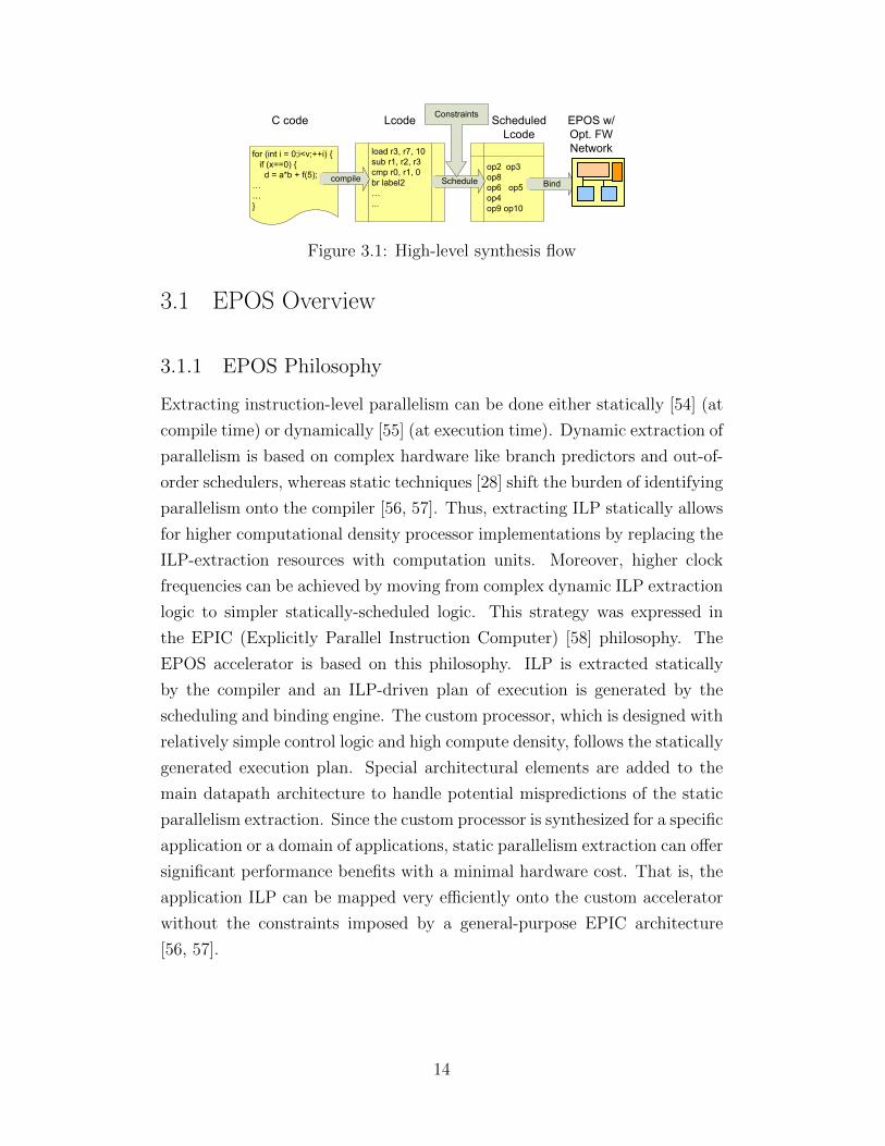
for (int i = 0;i<v;++i) {if (x==0) {d = a*b + f(5);
……}
load r3, r7, 10 sub r1, r2, r3cmp r0, r1, 0br label2…...
op2 op3 op8op6 op5 op4op9 op10
C code Lcode Scheduled Lcode
EPOS w/Opt. FW Network
compile Schedule Bind
Constraints
Figure 3.1: High-level synthesis flow
3.1 EPOS Overview
3.1.1 EPOS Philosophy
Extracting instruction-level parallelism can be done either statically [54] (at
compile time) or dynamically [55] (at execution time). Dynamic extraction of
parallelism is based on complex hardware like branch predictors and out-of-
order schedulers, whereas static techniques [28] shift the burden of identifying
parallelism onto the compiler [56, 57]. Thus, extracting ILP statically allows
for higher computational density processor implementations by replacing the
ILP-extraction resources with computation units. Moreover, higher clock
frequencies can be achieved by moving from complex dynamic ILP extraction
logic to simpler statically-scheduled logic. This strategy was expressed in
the EPIC (Explicitly Parallel Instruction Computer) [58] philosophy. The
EPOS accelerator is based on this philosophy. ILP is extracted statically
by the compiler and an ILP-driven plan of execution is generated by the
scheduling and binding engine. The custom processor, which is designed with
relatively simple control logic and high compute density, follows the statically
generated execution plan. Special architectural elements are added to the
main datapath architecture to handle potential mispredictions of the static
parallelism extraction. Since the custom processor is synthesized for a specific
application or a domain of applications, static parallelism extraction can offer
significant performance benefits with a minimal hardware cost. That is, the
application ILP can be mapped very efficiently onto the custom accelerator
without the constraints imposed by a general-purpose EPIC architecture
[56, 57].
14
3.1.2 EPOS Architecture
The main elements of the EPOS accelerator are the microcode memory
banks, which store all the datapath control information for the functional
units (FUs) that carry out the application computation. The microcode de-
tails the plan of execution as determined by the compiler and the high-level
synthesis engine. It is split in microwords, each of which controls the flow
of data in the processor datapath for one clock cycle. Each microword can
be split into multiple memory banks that are potentially placed close to the
datapath elements they control, thus facilitating better routing. There is also
a microcode address controller that holds the current microword to be exe-
cuted, and has address generation logic that determines the next microcode
word address. The functional units can have different characteristics in terms
of latency, pipeline and functionality characteristics.
As shown in Figure 3.2 there are two register files, one for application values
(RF) and one for predicate values (PRF). Moreover, each FU output is also
connected to a small shifting register file (SRF) where results may be stored
temporarily. The latest result produced by a functional unit is stored in the
top register of its respective SRF while previous values are shifted by one po-
sition further down in the SRF. This allows for predicated operations to be
speculated or, in other words, promoted over the predicate definition opera-
tion by a few cycles. Using the distributed SRFs offers several performance
and frequency advantages. Firstly, speculation of predicated operations can
be implemented without stalling or using a unified multiport shadow register
file for speculated results. Secondly, the existing RF writeback ports and
the FU forwarding paths can be used to store and forward, respectively, the
results of speculated operations that turn out to be true predicated. Simple
circuitry is used to squash the misspeculated operations while allowing the
rest to store their results in the register file.
Forwarding and register-file bypassing (RFB) are used to optimize the per-
formance of data-intensive applications. For a result produced by a FU in
cycle n, forwarding allows its use in cycle n+1 by the same or a different FU.
Forwarding paths are implemented with interconnection busses that commu-
nicate results from the output of FUs to their inputs without having to go
through the register file. Moreover, the use of forwarding paths eliminates
the need to store intermediate results that are alive for only one cycle in the
15
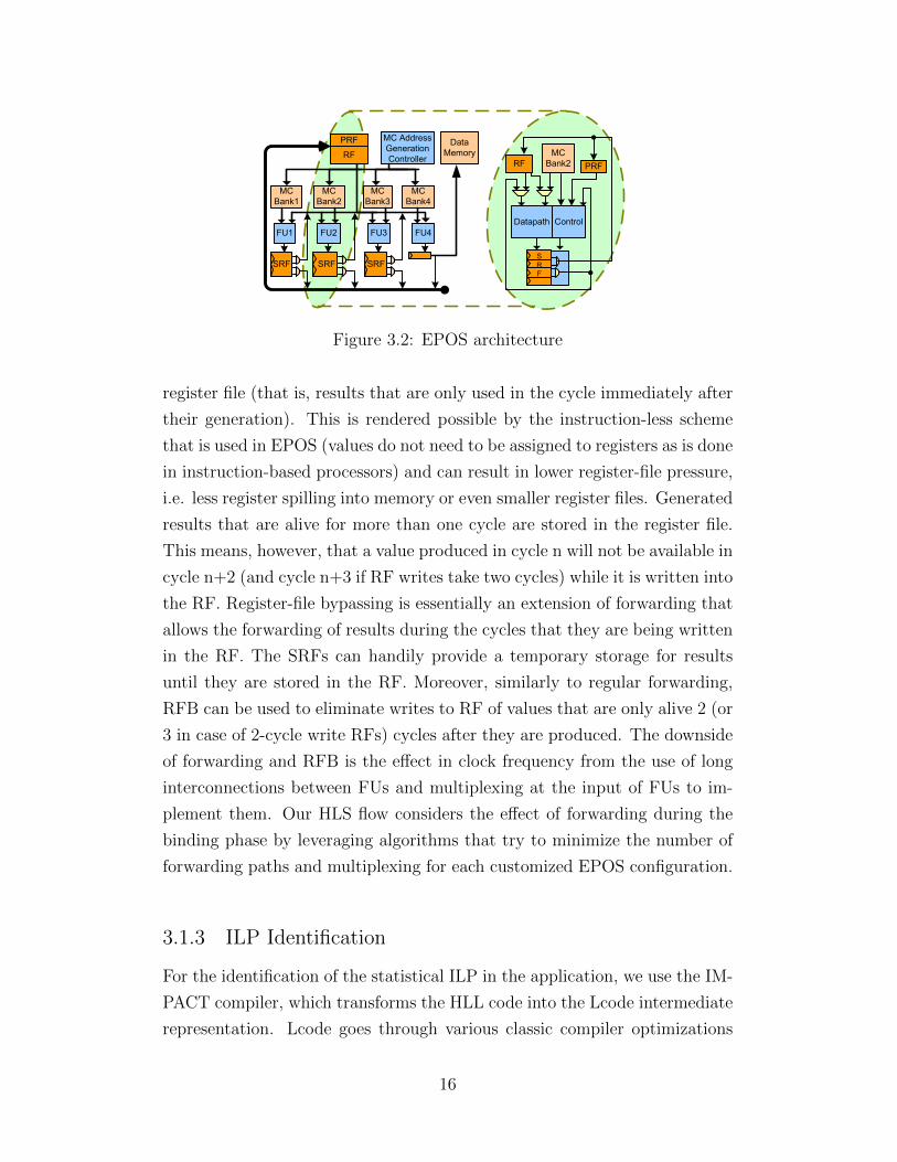
DataMemory
MCBank2
MCBank3
MCBank4
MC Address GenerationController
FU4
RF
PRF
MCBank1
FU1
SRF
FU3
SRF
FU2
SRF
MCBank2RF PRF
Datapath Control
SRF
Figure 3.2: EPOS architecture
register file (that is, results that are only used in the cycle immediately after
their generation). This is rendered possible by the instruction-less scheme
that is used in EPOS (values do not need to be assigned to registers as is done
in instruction-based processors) and can result in lower register-file pressure,
i.e. less register spilling into memory or even smaller register files. Generated
results that are alive for more than one cycle are stored in the register file.
This means, however, that a value produced in cycle n will not be available in
cycle n+2 (and cycle n+3 if RF writes take two cycles) while it is written into
the RF. Register-file bypassing is essentially an extension of forwarding that
allows the forwarding of results during the cycles that they are being written
in the RF. The SRFs can handily provide a temporary storage for results
until they are stored in the RF. Moreover, similarly to regular forwarding,
RFB can be used to eliminate writes to RF of values that are only alive 2 (or
3 in case of 2-cycle write RFs) cycles after they are produced. The downside
of forwarding and RFB is the effect in clock frequency from the use of long
interconnections between FUs and multiplexing at the input of FUs to im-
plement them. Our HLS flow considers the effect of forwarding during the
binding phase by leveraging algorithms that try to minimize the number of
forwarding paths and multiplexing for each customized EPOS configuration.
3.1.3 ILP Identification
For the identification of the statistical ILP in the application, we use the IM-
PACT compiler, which transforms the HLL code into the Lcode intermediate
representation. Lcode goes through various classic compiler optimizations
16
and also gets annotated with profile information. The profile annotation is
used to merge basic blocks into superblocks and hyperblocks. The generation
of coarser-granularity blocks can allow the scheduling engine to exploit more
parallelism.
Superblocks are formed by identifying frequently executed control paths
in the program that span many basic blocks. The basic blocks that com-
prise the identified control path are grouped into a single superblock that
may have multiple side exits but only one entry point at the head of the
block. Hyperblocks, on the other hand, differ from superblocks in the way
the selection of the basic blocks to be merged in a single block is done. In
particular, hyperblocks may group basic blocks that are executed in mutu-
ally exclusive control flow paths in the original program flow. To preserve
execution correctness, predicate values that express the branch conditions
of the exclusive paths are attached to the instructions of the merged basic
blocks. The instructions are executed or committed based on the values of
their attached predicates. Hyperblocks, like superblocks, may have multiple
side exits but only a single entry point.
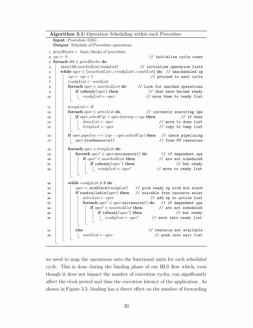
3.2 ILP-Driven Scheduling
After the identification of the statistical instruction-level parallelism and its
expression into superblocks and hyperblocks by the front-end compilation,
our scheduling engine focuses on the extraction of the maximum parallelism
under resource constraints. The superblocks, hyperblocks and basic blocks
contained in the generated Lcode are scheduled using an adapted version of
the list scheduling [59] algorithm. This algorithm is designed to handle the
intricacies of predication, speculation and operation reordering within blocks
that may contain more than one exit. Scheduling is performed on a per-
block basis, in order to maintain the parallelism that was identified within
superblocks and hyperblocks. The output of the scheduling phase is sched-
uled Lcode that honors the latency, pipeline and multitude characteristics of
the available FUs.
Initially, a direct acyclic graph (DAG), Gd = (V,A), is built based on
the dependence relations of the Lcode operations. Set V corresponds to
Lcode operations and set A corresponds to three different types of dependence
17
relations between the operations: (i) data dependencies (read-after-write),
(ii) predicate dependencies and (iii) flow dependencies
The data dependence arcs represent real dependencies between producer
and consumer operations. The dependencies of predicated operations on
predicate definition operations are represented with special predicate de-
pendence arcs. Differentiating between predicate and data dependencies is
mainly done in order to handle speculation of predicated operations which al-
lows us to exploit some extra ILP (as shown in Section 3.4). This is achieved
by using the flexibility of the temporary storage provided by the shift-register-
files to schedule predicated operations up to a few cycles ahead of the pred-
icate definition. Finally, the flow dependence arcs are used to ensure that
branch and store operations are executed in their original order within Lcode,
i.e. avoid speculation of memory writes. Mis-speculation of these types of
operations may lead to incorrect execution and requires complex hardware
to fix.
After the data dependence graph construction, slack values are computed
for each node of the graph. Two slack metrics are used to determine the
criticality of operations: local slack and global slack. Local slack is calculated
within the operation’s containing block and represents the criticality of the
operation when the dynamic control flow does not follow any of the block
side branches. Global slack, on the other hand, is calculated based on the
function-wide dependencies and represents the criticality of the operation
when side branches are also considered. Local and global slacks are used in a
weighted function to determine the total slack. The relative weighting of the
local and global slacks determines a balance between ILP optimization for
the statistically likely case vs. the statistically unlikely case. For example,
assume the following operation sequence within a superblock: op1→br→op2,
where a side branch (br) exists between two operations (op1 and op2). Let us
assume that operation op2 has a relatively lower local slack (op2 locally more
critical) and operation op1 has a relatively lower global slack (op1 globally
more critical). Then if the local slack weighting is much higher than the
global slack, operation op2 will be executed before operation op1, which will
potentially lead to a shorter execution latency in case the control flow follows
the statistically most likely control path through the final exit of the block.
However, in the case that the control flow falls through the side exit (less
likely flow) we will have executed a redundant operation (op2) that may
18
result in longer execution latency. On the other hand, if slack weighting
favors global slacks, operation op1 will be executed before op2, optimizing
the case that the control flow follows the side branch.
Subsequently, our modified list-scheduling algorithm is performed on a
per-block basis taking into consideration the different types of dependencies.
For example, data-dependent operations cannot enter the ready list until the
corresponding data producing operation is scheduled and finished executing,
that is, only if the data producing operation belongs in the same block. On
the other hand, predicate-dependent operations in a system with SRFs can
be scheduled a number of cycles, equal to the SRF depth, ahead of their
predicate producer. Flow dependencies are also not as strict dependencies as
data dependencies. In particular a flow-dependent operation can be sched-
uled to complete its execution in the same cycle with the operation it is
dependent on. For example a store operation can be scheduled in the same
cycle with a branch that it is flow-dependent on. If the branch turns out to
be taken, the operation-squashing logic (used for false predicated operations)
can terminate the store operation before it writes into memory.
An overview of the scheduling algorithm is given in Algorithm 3.1 for the
case in which register file bypassing is enabled. The operations are handled
with the help of six lists. Initially operations are assigned to the ready-list
and the unshed-list depending on whether they are ready to execute or they
are dependent on operations that have not executed yet. The wait-list is used
to hold operations that would be ready to execute if enough resources were
available. The active-list is used to hold operations that are currently being
computed. Finally done-list is used to hold all the operations that have
finished execution while temp-list holds only the operations that finished
execution during the current cycle.
3.3 Forwarding Path Aware Binding
At the end of the scheduling phase, we get a feasible timing plan of exe-
cution for all the operations of the application based on the number and
type of available functional units and the assumption that every computed
value can be forwarded to any FU. However, before we can generate the mi-
crocode (MC) words that will be loaded on the EPOS MC memory banks,
19
Algorithm 3.1: Operation Scheduling within each ProcedureInput: Procedure DAGOutput: Schedule of Procedure operations
1 procBlocks← basic blocks of procedure2 cyc← 0 // initialize cycle count
3 foreach blk ∈ procBlocks do4 init(blk,unschedList,readyList) // initialize operation lists
5 while oper ∈ {unschedList ∪ readyList ∪ waitList} do // unscheduled op
6 cyc← cyc + 1 // proceed to next cycle
7 readyList← waitList8 foreach oper ∈ unschedList do // Look for unsched operations
9 if isReady(oper) then // that have become ready
10 readyList← oper // move them to ready list
11 tempList← ∅12 foreach oper ∈ activList do // currently executing ops
13 if oper.schedCyc + oper.latency = cyc then // if done
14 doneList← oper // move to done list
15 tempList← oper // copy to temp list
16 if oper.pipeline == (cyc− oper.schedCyc) then // check pipelining
17 oper.freeResource() // free FU resources
18 foreach oper ∈ tempList do19 foreach oper′ ∈ oper.successors() do // if dependent ops
20 if oper′ ∈ unschedList then // are not scheduled
21 if isReady(oper’) then // but ready
22 readyList← oper′ // move to ready list
23 while readyList 6= ∅ do24 oper ← minSlack(readyList) // pick ready op with min slack
25 if resAvailable(oper) then // suitable free resource exist
26 activList← oper // add op to active list
27 foreach oper′ ∈ oper.successors() do // if dependent ops
28 if oper′ ∈ unschedList then // are not scheduled
29 if isReady(oper’) then // but ready
30 readyList← oper′ // move into ready list
31 else // resource not available
32 waitList← oper // push into wait list
we need to map the operations onto the functional units for each scheduled
cycle. This is done during the binding phase of our HLS flow which, even
though it does not impact the number of execution cycles, can significantly
affect the clock period and thus the execution latency of the application. As
shown in Figure 3.3, binding has a direct effect on the number of forwarding
20
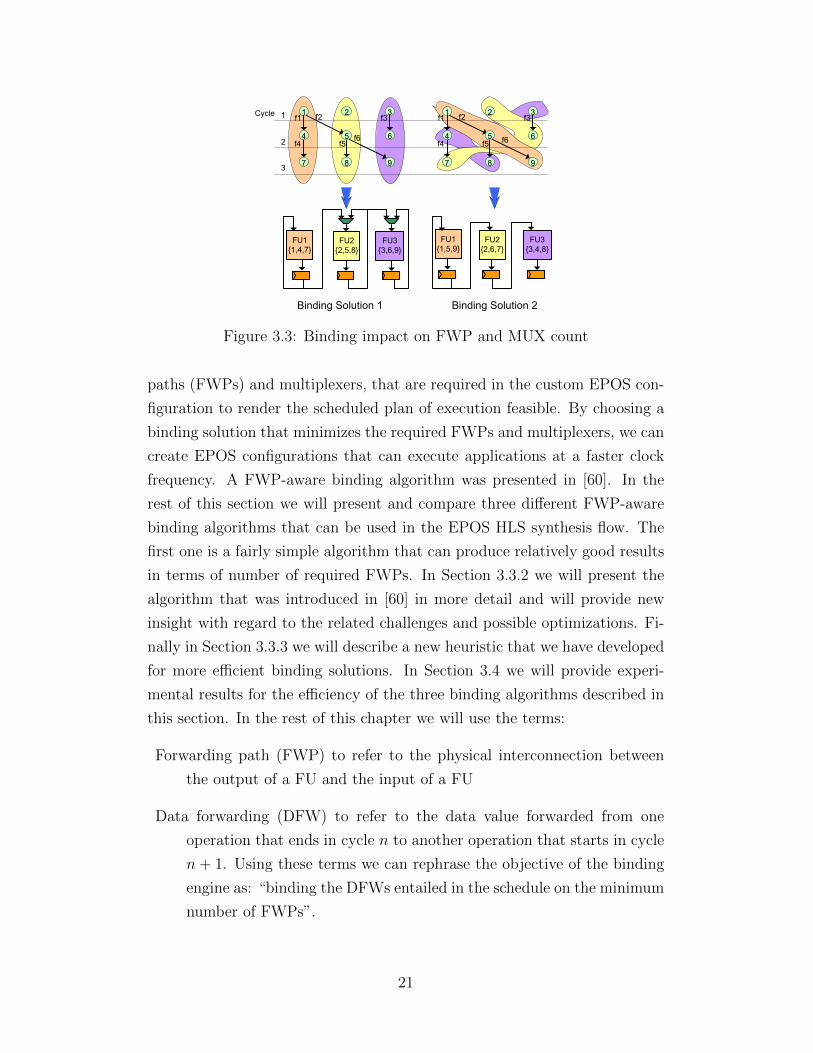
1
7
Cycle 1
2
3
Binding Solution 1
f1
f44
2
8
f2
f55
3
9
f3
f6 6
1
7
f1
f44
2
8
f2
f55
3
9
f3
f6 6
FU1{1,4,7}
FU2{2,5,8}
FU3{3,6,9}
FU1{1,5,9}
FU2{2,6,7}
FU3{3,4,8}
Binding Solution 2
Figure 3.3: Binding impact on FWP and MUX count
paths (FWPs) and multiplexers, that are required in the custom EPOS con-
figuration to render the scheduled plan of execution feasible. By choosing a
binding solution that minimizes the required FWPs and multiplexers, we can
create EPOS configurations that can execute applications at a faster clock
frequency. A FWP-aware binding algorithm was presented in [60]. In the
rest of this section we will present and compare three different FWP-aware
binding algorithms that can be used in the EPOS HLS synthesis flow. The
first one is a fairly simple algorithm that can produce relatively good results
in terms of number of required FWPs. In Section 3.3.2 we will present the
algorithm that was introduced in [60] in more detail and will provide new
insight with regard to the related challenges and possible optimizations. Fi-
nally in Section 3.3.3 we will describe a new heuristic that we have developed
for more efficient binding solutions. In Section 3.4 we will provide experi-
mental results for the efficiency of the three binding algorithms described in
this section. In the rest of this chapter we will use the terms:
Forwarding path (FWP) to refer to the physical interconnection between
the output of a FU and the input of a FU
Data forwarding (DFW) to refer to the data value forwarded from one
operation that ends in cycle n to another operation that starts in cycle
n+ 1. Using these terms we can rephrase the objective of the binding
engine as: “binding the DFWs entailed in the schedule on the minimum
number of FWPs”.
21
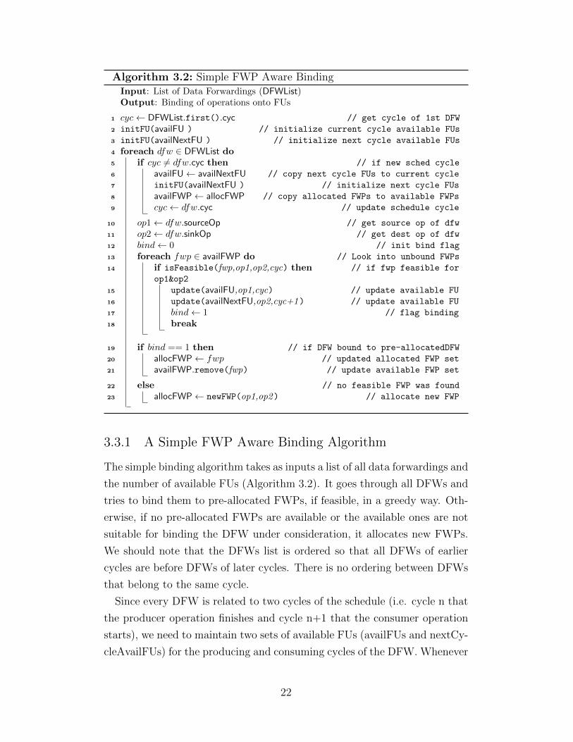
Algorithm 3.2: Simple FWP Aware BindingInput: List of Data Forwardings (DFWList)Output: Binding of operations onto FUs
1 cyc← DFWList.first().cyc // get cycle of 1st DFW
2 initFU(availFU ) // initialize current cycle available FUs
3 initFU(availNextFU ) // initialize next cycle available FUs
4 foreach dfw ∈ DFWList do5 if cyc 6= dfw.cyc then // if new sched cycle
6 availFU← availNextFU // copy next cycle FUs to current cycle
7 initFU(availNextFU ) // initialize next cycle FUs
8 availFWP← allocFWP // copy allocated FWPs to available FWPs
9 cyc← dfw.cyc // update schedule cycle
10 op1← dfw.sourceOp // get source op of dfw
11 op2← dfw.sinkOp // get dest op of dfw
12 bind← 0 // init bind flag
13 foreach fwp ∈ availFWP do // Look into unbound FWPs
14 if isFeasible(fwp,op1,op2,cyc) then // if fwp feasible for
op1&op2
15 update(availFU,op1,cyc) // update available FU
16 update(availNextFU,op2,cyc+1) // update available FU
17 bind← 1 // flag binding
18 break
19 if bind == 1 then // if DFW bound to pre-allocatedDFW
20 allocFWP← fwp // updated allocated FWP set
21 availFWP.remove(fwp) // update available FWP set
22 else // no feasible FWP was found
23 allocFWP← newFWP(op1,op2) // allocate new FWP
3.3.1 A Simple FWP Aware Binding Algorithm
The simple binding algorithm takes as inputs a list of all data forwardings and
the number of available FUs (Algorithm 3.2). It goes through all DFWs and
tries to bind them to pre-allocated FWPs, if feasible, in a greedy way. Oth-
erwise, if no pre-allocated FWPs are available or the available ones are not
suitable for binding the DFW under consideration, it allocates new FWPs.
We should note that the DFWs list is ordered so that all DFWs of earlier
cycles are before DFWs of later cycles. There is no ordering between DFWs
that belong to the same cycle.
Since every DFW is related to two cycles of the schedule (i.e. cycle n that
the producer operation finishes and cycle n+1 that the consumer operation
starts), we need to maintain two sets of available FUs (availFUs and nextCy-
cleAvailFUs) for the producing and consuming cycles of the DFW. Whenever
22
the next cycle becomes the current cycle, availFUs is initialized with nextCy-
cleAvailFUs and nextCycleAvailFUs is initialized with a full set of all FUs
available. There are also two sets of FWPs maintained (allocFWPs and avail-
FWPs); allocFWPs holds all the allocated FWPs, whereas availFWPs stores
a set of the available FWPs that can be considered for binding the unbound
DFWs in the current cycle. The allocFWPs set is updated every time a
new FWP is allocated and the availFWP set is updated for every DFW that
gets bound to a pre-allocated FWP and also every time the current cycle is
incremented.
In the simple binding algorithm, DFWs are bound by explicitly mapping
operations onto specific FUs. This way, a feasible solution that honors func-
tional unit resource constraints is derived at the end of the iteration over
all DFWs. In this solution all allocated FWPs are explicit in the sense that
they are described by a source FU id and a sink FU id. As we will see in
the next subsections, the more sophisticated algorithms use implicit FWPs
which then are mapped onto explicit physical FWPs.
3.3.2 Network Flow Binding Algorithm
The network-flow (netflow) algorithm is based on a transformation of the
EPOS binding problem into a clique partitioning one. A network flow for-
mulation is used to solve the clique partitioning. A post-processing phase
may be required to make the network solution feasible for our schedule.
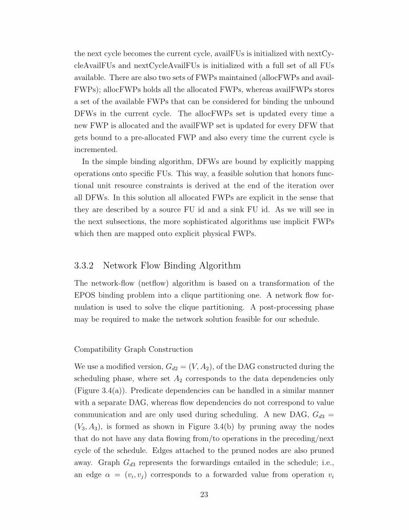
Compatibility Graph Construction
We use a modified version, Gd2 = (V,A2), of the DAG constructed during the
scheduling phase, where set A2 corresponds to the data dependencies only
(Figure 3.4(a)). Predicate dependencies can be handled in a similar manner
with a separate DAG, whereas flow dependencies do not correspond to value
communication and are only used during scheduling. A new DAG, Gd3 =
(V3, A3), is formed as shown in Figure 3.4(b) by pruning away the nodes
that do not have any data flowing from/to operations in the preceding/next
cycle of the schedule. Edges attached to the pruned nodes are also pruned
away. Graph Gd3 represents the forwardings entailed in the schedule; i.e.,
an edge α = (vi, vj) corresponds to a forwarded value from operation vi
23
Cycle
1
2
3
4
5
a) Gd2 b) Gd3
f2 f3
f4
f7 f8
f1 f2 f3
f4f6f5
f7 f8
f1 f2 f3
f4
f7 f8
c) Gc
f1 f2 f3
f4
f7 f8
f1
d) Cliques
Figure 3.4: Building the compatibility graph from the data-dependencegraph
to vj. A compatibility graph Gc = (Vc, Ac) for these forwardings (FWs)
can then be constructed, as shown in Figure 3.4(c). Note that the nodes
in Vc do not represent the operation nodes in Gd3 but correspond to the
DFWs (i.e. the edges of Gd3) involved in the schedule. A directed edge
αc = {(vm, vn) | vm ∈ Vc, vn ∈ Vc} is drawn between two vertices, if the
producer operation of the DFW vm is scheduled to finish in an earlier cycle
than the producing operation of DFW vn. Each edge αc is assigned a weight
wmn, which represents the cost of binding vm and vn to the same FWP.
Given a data forwarding pattern represented by the compatibility graph
Gc, our goal is to find an edge subset in Gc that covers all the vertices in Vc in
such a way that the sum of the edge weights is minimum with the constraint
that all the vertices can be bound to no more than k FWPs, where k is
the minimum number of FWPs required to fulfill the schedule. This can be
translated into a clique partitioning problem, where each clique corresponds
to the DFWs that can be bound into a single FWP (Figure 3.4(d)).
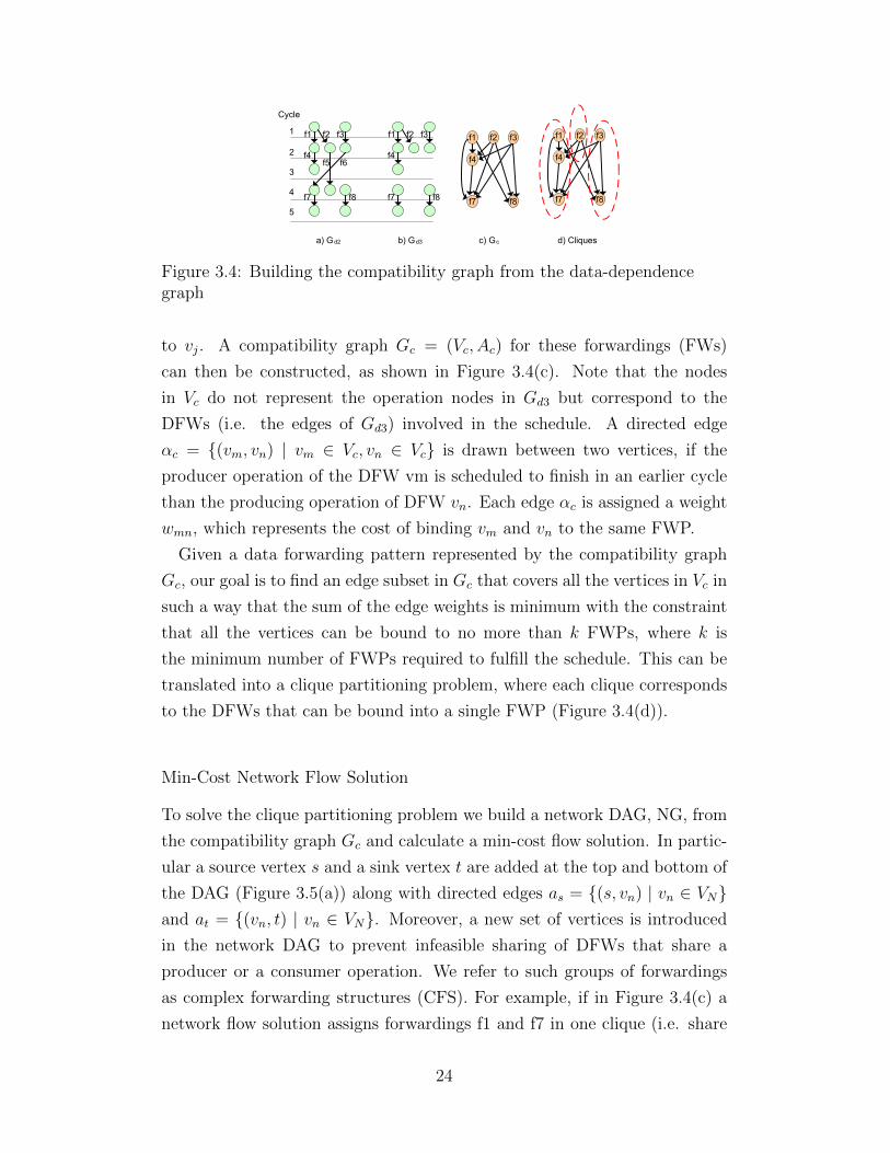
Min-Cost Network Flow Solution
To solve the clique partitioning problem we build a network DAG, NG, from
the compatibility graph Gc and calculate a min-cost flow solution. In partic-
ular a source vertex s and a sink vertex t are added at the top and bottom of
the DAG (Figure 3.5(a)) along with directed edges as = {(s, vn) | vn ∈ VN}and at = {(vn, t) | vn ∈ VN}. Moreover, a new set of vertices is introduced
in the network DAG to prevent infeasible sharing of DFWs that share a
producer or a consumer operation. We refer to such groups of forwardings
as complex forwarding structures (CFS). For example, if in Figure 3.4(c) a
network flow solution assigns forwardings f1 and f7 in one clique (i.e. share
24
a) N G
f2' f3'
f4
f7
f8
f1'c
s
t
f2 f3f1
c’
f8'
f4'
f7'
f4
f7
f8
c
s
t
f2 f3f1
b) Split Node NG
Figure 3.5: Building the network graph
a FWP) and forwardings f2 and f8 in a second clique (i.e. share a second
FWP), it would not be a feasible solution (that is, f1 and f2 imply that the
two FWPs begin at the output of the same FU, while f2 and f8 imply that
the two FWPs begin at the output of different FUs). In order to avoid this
infeasible binding we add vertex c (Figure 3.5(a)) in between the pair of for-
wardings f1-f2 and other singular forwardings (i.e. FWs that do not share
producer or consumer operations) in later cycles. Finally, the network DAG
is further modified by the split-node technique [61] which ensures that each
node is traversed by a single flow. This is achieved by splitting each node into
two nodes connected with a directed edge of a single capacity (Figure 3.5(b)).
By assigning cost and capacity values to each edge through a cost function
C and a capacity function K, respectively, we conclude the transformation of
the compatibility graph Gc into the network graph NG = (s, t, VN , AN , C,K).
The cost, C, of the network edges tries to capture, among other things, the
similarity of the neighboring forwarding patterns of two compatible FWs, so
as to lead to better solutions. The Fschema parameter is used to represent
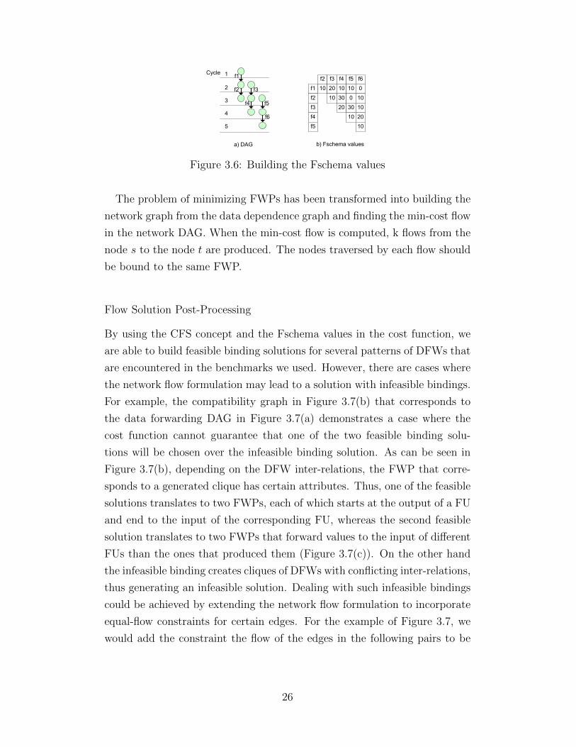
this factor and it is calculated based on Gd3. For example, let us consider the
DAG shown in Figure 3.6(a). The minimum number of FWPs required to
satisfy this schedule is two. However, in order to produce a feasible binding
with two FWPs, f1, f3 and f5 need to be bound to the same FWP while f2, f4
and f6 are bound to a second FWP. Otherwise, 3 FWPs will be required. This
can be fulfilled with the help of the Fschema value. Fschema is calculated
by trying to find the maximum match in the neighboring FW patterns. In
Figure 3.6(b), the bigger values produced for pairs f2-f4 and f3-f5 show that
these pairs of forwardings have more similarities in their FW neighboring
patterns. These values can help bias the network flow to find better solutions
by binding similar pairs together.
25
Cycle 1
2
3
4
5
a) DAG
f1
f2
f4
f3
f6
f5
b) Fschema values
f1
f2
f3
f4
f5
f2
10
f3
20
10
f4
10
30
20
f5
10
0
30
10
f6
0
10
10
20
10
Figure 3.6: Building the Fschema values
The problem of minimizing FWPs has been transformed into building the
network graph from the data dependence graph and finding the min-cost flow
in the network DAG. When the min-cost flow is computed, k flows from the
node s to the node t are produced. The nodes traversed by each flow should
be bound to the same FWP.
Flow Solution Post-Processing
By using the CFS concept and the Fschema values in the cost function, we
are able to build feasible binding solutions for several patterns of DFWs that
are encountered in the benchmarks we used. However, there are cases where
the network flow formulation may lead to a solution with infeasible bindings.
For example, the compatibility graph in Figure 3.7(b) that corresponds to
the data forwarding DAG in Figure 3.7(a) demonstrates a case where the
cost function cannot guarantee that one of the two feasible binding solu-
tions will be chosen over the infeasible binding solution. As can be seen in
Figure 3.7(b), depending on the DFW inter-relations, the FWP that corre-
sponds to a generated clique has certain attributes. Thus, one of the feasible
solutions translates to two FWPs, each of which starts at the output of a FU
and end to the input of the corresponding FU, whereas the second feasible
solution translates to two FWPs that forward values to the input of different
FUs than the ones that produced them (Figure 3.7(c)). On the other hand
the infeasible binding creates cliques of DFWs with conflicting inter-relations,
thus generating an infeasible solution. Dealing with such infeasible bindings
could be achieved by extending the network flow formulation to incorporate
equal-flow constraints for certain edges. For the example of Figure 3.7, we
would add the constraint the flow of the edges in the following pairs to be
26
Cycle
1
2
3
4
a) Gd2 b) G c
f4
f7
f1 f2
f3
f1
f4
f5 f6
f4
f7
f1
FU1 FU3
c) Feasible FWPs
Feasible Infeasible
Figure 3.7: Effect of flow on binding feasibility
equal:
(f1, f3) ≡ (f3, f5) ∧ (f2, f4) ≡ (f4, f6)
(f1, f4) ≡ (f4, f5) ∧ (f2, f3) ≡ (f3, f6)
The min-cost problem flow problem with equal-flow constraints has been
shown to be NP-hard [62]. In [63] they used integer-linear-programming tech-
niques to solve the problem of network min-cost with equal flow, whereas in
[64] they proposed clever heuristics to efficiently solve the equal flow prob-
lem. In this work we use a post-fix phase during which the min-cost solution
is checked and fixed by unbinding the DFWs that cause the infeasibility and
binding them to different pre-allocated FWPs or new FWPs. Further details
on how the check and fix is done are provided in [60].
3.3.3 Clustered Binding
As we saw in the previous subsection, DFWs form complicated inter-relations
with each other and choosing a feasible binding of the DFWs in cycle n+ 1
is dependent on how the DFWs in cycle n were bound. However, in the case
that there are no DFWs scheduled in cycle n, the binding decisions for cycles
n + 1 and thereafter can be independent of how DFWs scheduled earlier
than cycle n were bound. Based on this observation we partition the DFWs
into clusters, where a cluster is defined as a set of DFWs that are scheduled
between cycle n and n + k and for each cycle within [n, n + k] there is at
least one scheduled DFW that belongs to the DFW set. As the name of this
algorithm implies, binding is done on a per-cluster basis, while seeking to
achieve maximum FWP sharing both at the intra-cluster (i.e. within cycles
of the cluster) and the inter-cluster (i.e. across clusters) level.
27
Cluster Setup
Initially, the application DFWs are divided into clusters according to the
previous definition. Each cycle in every cluster is assigned a complexity value
based on a weighted function of the number of scheduled DFWs and the
presence of CFSs. The role of the complexity value is to provide a measure
of the probability that a feasible binding of the cycle’s DFWs will require
extra FWPs to be allocated. For each cluster the cycle with the maximum
complexity is identified and the average complexity of the cluster is computed
as the sum of all the cluster cycle complexities divided by the number of
cycles in the cluster. The average complexity is used to order the clusters in
decreasing order, so that binding can begin from the clusters with the highest
average complexity to the ones with the lowest average complexity. Binding
the lower complexity clusters later is likely to create more chances for FWP
sharing and thus fewer FWPs. The cycle with the maximum complexity
in each cluster is the first cycle to be bound during each cluster binding,
following the same philosophy as described above.
Cluster Binding
For each cluster, binding is done cycle-by-cycle starting with the cluster cycle
that is identified as of the highest complexity. For each cycle the pre-allocated
FWPs are first considered. If there are more DFWs than pre-allocated FWPs,
or the pre-allocated FWPs do not lend themselves for feasible bindings, new
FWPs are allocated. Before binding the DFWs to the pre-allocated FWPs,
a compatibility computation function is called. This function computes a
compatibility value for each pair of DFWs and FWPs. The compatibility
value represents the suitability of binding the respective FWP on the DFW
with regards to the inter-relations of the DFW with its neighboring DFWs
in the previous, the current and the next cycles of the cluster. Binding
the DFWs to the pre-allocated FWPs is done in decreasing order of the
compatibility values.
28
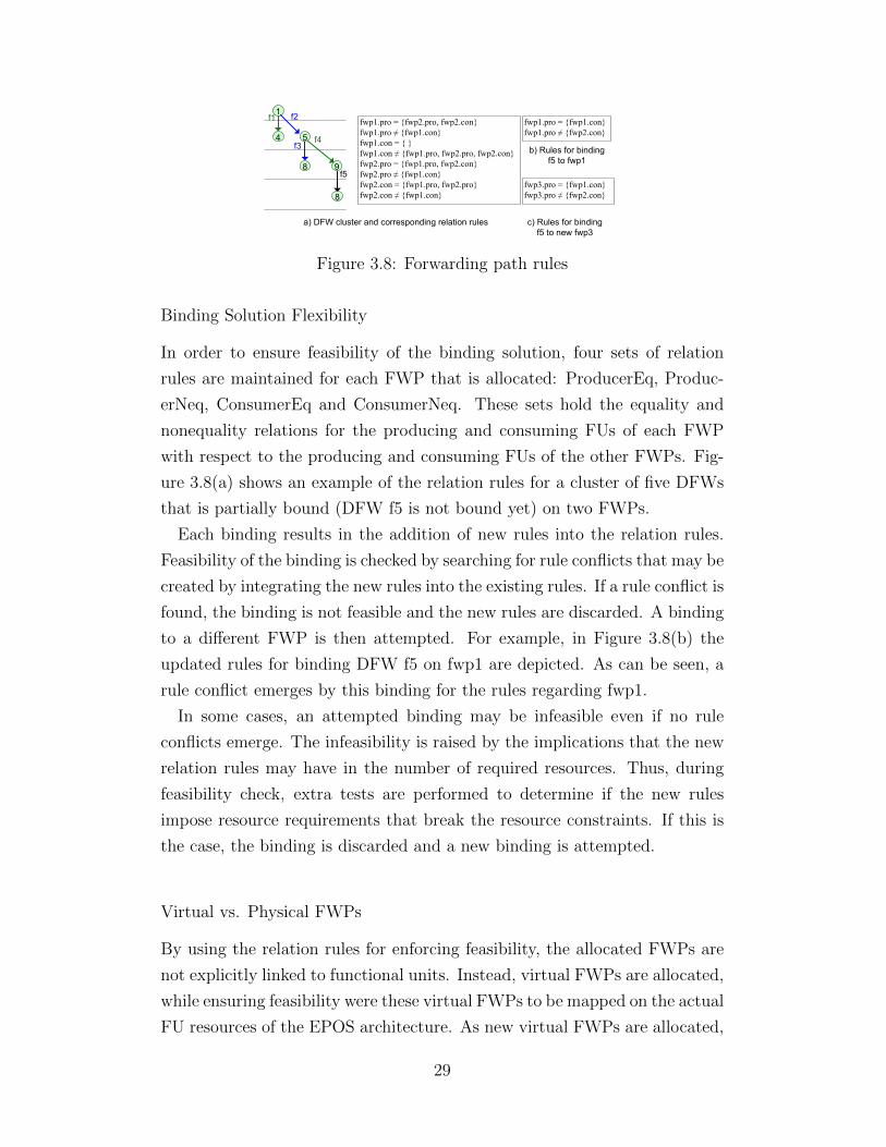
1f1
4
8
f2
f35
9
f4
8
f5
fwp1.pro = {fwp2.pro, fwp2.con}fwp1.pro ≠ {fwp1.con}fwp1.con = { }fwp1.con ≠ {fwp1.pro, fwp2.pro, fwp2.con}fwp2.pro = {fwp1.pro, fwp2.con}fwp2.pro ≠ {fwp1.con}fwp2.con = {fwp1.pro, fwp2.pro}fwp2.con ≠ {fwp1.con}
fwp1.pro = {fwp1.con}fwp1.pro ≠ {fwp2.con}
fwp3.pro = {fwp1.con}fwp3.pro ≠ {fwp2.con}
a) DFW cluster and corresponding relation rules
b) Rules for binding f5 to fwp1
c) Rules for binding f5 to new fwp3
Figure 3.8: Forwarding path rules
Binding Solution Flexibility
In order to ensure feasibility of the binding solution, four sets of relation
rules are maintained for each FWP that is allocated: ProducerEq, Produc-
erNeq, ConsumerEq and ConsumerNeq. These sets hold the equality and
nonequality relations for the producing and consuming FUs of each FWP
with respect to the producing and consuming FUs of the other FWPs. Fig-
ure 3.8(a) shows an example of the relation rules for a cluster of five DFWs
that is partially bound (DFW f5 is not bound yet) on two FWPs.
Each binding results in the addition of new rules into the relation rules.
Feasibility of the binding is checked by searching for rule conflicts that may be
created by integrating the new rules into the existing rules. If a rule conflict is
found, the binding is not feasible and the new rules are discarded. A binding
to a different FWP is then attempted. For example, in Figure 3.8(b) the
updated rules for binding DFW f5 on fwp1 are depicted. As can be seen, a
rule conflict emerges by this binding for the rules regarding fwp1.
In some cases, an attempted binding may be infeasible even if no rule
conflicts emerge. The infeasibility is raised by the implications that the new
relation rules may have in the number of required resources. Thus, during
feasibility check, extra tests are performed to determine if the new rules
impose resource requirements that break the resource constraints. If this is
the case, the binding is discarded and a new binding is attempted.
Virtual vs. Physical FWPs
By using the relation rules for enforcing feasibility, the allocated FWPs are
not explicitly linked to functional units. Instead, virtual FWPs are allocated,
while ensuring feasibility were these virtual FWPs to be mapped on the actual
FU resources of the EPOS architecture. As new virtual FWPs are allocated,
29
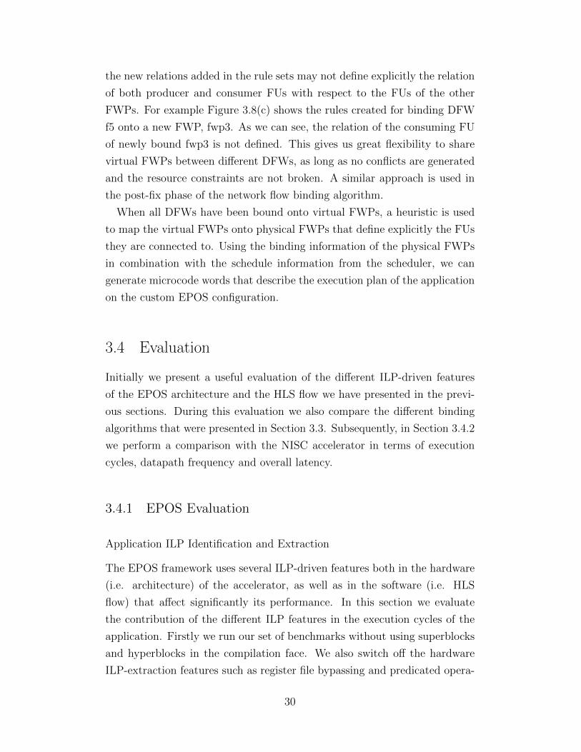
the new relations added in the rule sets may not define explicitly the relation
of both producer and consumer FUs with respect to the FUs of the other
FWPs. For example Figure 3.8(c) shows the rules created for binding DFW
f5 onto a new FWP, fwp3. As we can see, the relation of the consuming FU
of newly bound fwp3 is not defined. This gives us great flexibility to share
virtual FWPs between different DFWs, as long as no conflicts are generated
and the resource constraints are not broken. A similar approach is used in
the post-fix phase of the network flow binding algorithm.
When all DFWs have been bound onto virtual FWPs, a heuristic is used
to map the virtual FWPs onto physical FWPs that define explicitly the FUs
they are connected to. Using the binding information of the physical FWPs
in combination with the schedule information from the scheduler, we can
generate microcode words that describe the execution plan of the application
on the custom EPOS configuration.
3.4 Evaluation
Initially we present a useful evaluation of the different ILP-driven features
of the EPOS architecture and the HLS flow we have presented in the previ-
ous sections. During this evaluation we also compare the different binding
algorithms that were presented in Section 3.3. Subsequently, in Section 3.4.2
we perform a comparison with the NISC accelerator in terms of execution
cycles, datapath frequency and overall latency.
3.4.1 EPOS Evaluation
Application ILP Identification and Extraction
The EPOS framework uses several ILP-driven features both in the hardware
(i.e. architecture) of the accelerator, as well as in the software (i.e. HLS
flow) that affect significantly its performance. In this section we evaluate
the contribution of the different ILP features in the execution cycles of the
application. Firstly we run our set of benchmarks without using superblocks
and hyperblocks in the compilation face. We also switch off the hardware
ILP-extraction features such as register file bypassing and predicated opera-
30
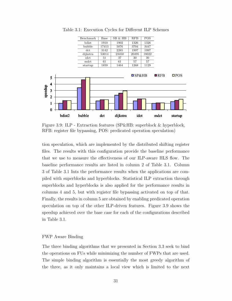
Table 3.1: Execution Cycles for Different ILP Schemes
Benchmark Base SB & HB RFB POS
bdist 1910 1902 1326 1326bubble 17413 5076 3704 3447dct 3142 2285 1997 1997
dijkstra 53014 23450 20495 18022idct 51 37 30 30mdct 61 61 57 57
startup 1859 1464 1268 1129
5 SP&HB RFB POS
345
edup
SP&HB RFB POS
012345
spee
dup
SP&HB RFB POS
012345
bdist2 bubble dct dijkstra idct mdct startup
spee
dup
SP&HB RFB POS
012345
bdist2 bubble dct dijkstra idct mdct startup
spee
dup
SP&HB RFB POS
012345
bdist2 bubble dct dijkstra idct mdct startup
spee
dup
SP&HB RFB POS
Figure 3.9: ILP - Extraction features (SP&HB: superblock & hyperblock,RFB: register file bypassing, POS: predicated operation speculation)
tion speculation, which are implemented by the distributed shifting register
files. The results with this configuration provide the baseline performance
that we use to measure the effectiveness of our ILP-aware HLS flow. The
baseline performance results are listed in column 2 of Table 3.1. Column
3 of Table 3.1 lists the performance results when the applications are com-
piled with superblocks and hyperblocks. Statistical ILP extraction through
superblocks and hyperblocks is also applied for the performance results in
columns 4 and 5, but with register file bypassing activated on top of that.
Finally, the results in column 5 are obtained by enabling predicated operation
speculation on top of the other ILP-driven features. Figure 3.9 shows the
speedup achieved over the base case for each of the configurations described
in Table 3.1.
FWP Aware Binding
The three binding algorithms that we presented in Section 3.3 seek to bind
the operations on FUs while minimizing the number of FWPs that are used.
The simple binding algorithm is essentially the most greedy algorithm of
the three, as it only maintains a local view which is limited to the next
31
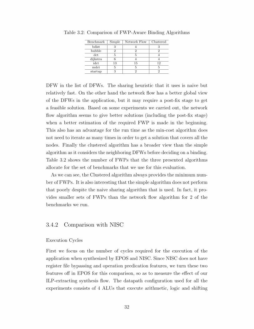
Table 3.2: Comparison of FWP-Aware Binding Algorithms
Benchmark Simple Network Flow Clustered
bdist 3 4 3bubble 2 2 2dct 5 5 4
dijkstra 6 4 4idct 13 15 12mdct 5 5 5
startup 3 2 2
DFW in the list of DFWs. The sharing heuristic that it uses is naive but
relatively fast. On the other hand the network flow has a better global view
of the DFWs in the application, but it may require a post-fix stage to get
a feasible solution. Based on some experiments we carried out, the network
flow algorithm seems to give better solutions (including the post-fix stage)
when a better estimation of the required FWP is made in the beginning.
This also has an advantage for the run time as the min-cost algorithm does
not need to iterate as many times in order to get a solution that covers all the
nodes. Finally the clustered algorithm has a broader view than the simple
algorithm as it considers the neighboring DFWs before deciding on a binding.
Table 3.2 shows the number of FWPs that the three presented algorithms
allocate for the set of benchmarks that we use for this evaluation.
As we can see, the Clustered algorithm always provides the minimum num-
ber of FWPs. It is also interesting that the simple algorithm does not perform
that poorly despite the naive sharing algorithm that is used. In fact, it pro-
vides smaller sets of FWPs than the network flow algorithm for 2 of the
benchmarks we run.
3.4.2 Comparison with NISC
Execution Cycles
First we focus on the number of cycles required for the execution of the
application when synthesized by EPOS and NISC. Since NISC does not have
register file bypassing and operation predication features, we turn these two
features off in EPOS for this comparison, so as to measure the effect of our
ILP-extracting synthesis flow. The datapath configuration used for all the
experiments consists of 4 ALUs that execute arithmetic, logic and shifting
32
Table 3.3: NISC vs. EPOS: Cycles
Benchmark NISC EPOS (SB&HB) Speedup
bdist 2110 1902 1.11bubble 31247 5076 6.16dct 4920 2285 2.15
dijkstra 104610 23450 4.46mdct 146 61 2.39
startup 2838 1464 1.94
Average 3.03
operations, 1 multiplier, and 1 LD/ST unit.
In Table 3.3 we can see that there is a significant decrease in execution
cycles for almost all benchmarks when they are synthesized on EPOS. The
speedup gained in EPOS ranges from 1.11 to 6.16, with an average value of
just over 3.
Clock Frequency
In order to evaluate our forwarding path binding technique we compare the
critical paths of the synthesized processors. The data and control memories
are stripped off in both NISC and EPOS and only the datapath, the register
file and the FWPs with the multiplexers are synthesized. Synthesis and
timing analysis were done in Altera’s Quartus II environment. First, we
built EPOS with all the possible FWPs (i.e. without any FWP optimization).
Then, we performed the binding optimization to optimize FWPs. The results
are listed in Tables 3.4 and 3.5. The second column“UnOpt EPOS” shows
the results for the unoptimized EPOS, i.e the EPOS with a full set of FWPs.
Table 3.4 lists the reported frequencies and Table 3.5 shows the total size
of the multiplexers (i.e. the total number of mux inputs). We can see that
there is a correlation between the frequency and the MUX size. The binding
optimization of EPOS minimizes the number of FWPs which has a large
impact on the total required size of multiplexing and consequently on the
critical path delays. We can observe that compared to unoptimized EPOS,
the optimized EPOS reports up to 41% improvement on frequency and up
to 62% reduction on total MUX size. Compared to NISC, EPOS achieves
higher clock frequencies in most cases, while the MUX size is on average the
same. By combining the execution cycles with the achieved frequency for
both processors we can compare the benchmark execution latencies. These
results are shown in Figure 3.10 and an average speedup of 3.34X over NISC
33
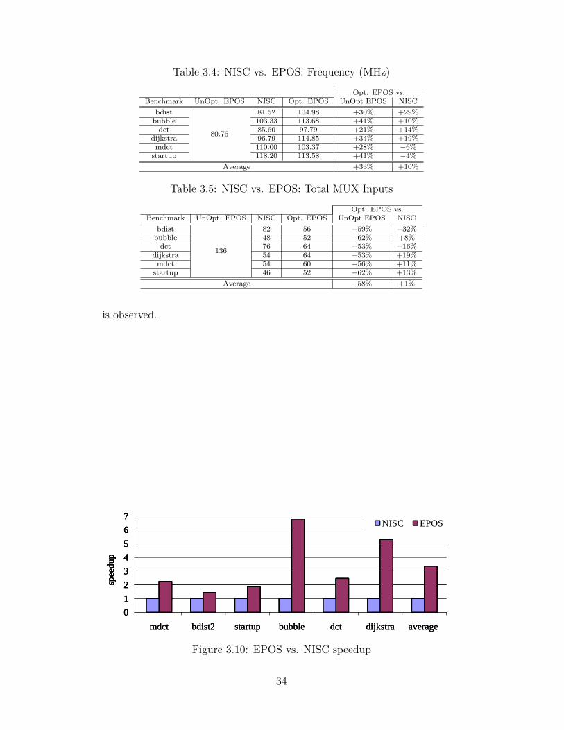
Table 3.4: NISC vs. EPOS: Frequency (MHz)
Opt. EPOS vs.Benchmark UnOpt. EPOS NISC Opt. EPOS UnOpt EPOS NISC
bdist
80.76
81.52 104.98 +30% +29%bubble 103.33 113.68 +41% +10%dct 85.60 97.79 +21% +14%
dijkstra 96.79 114.85 +34% +19%mdct 110.00 103.37 +28% −6%
startup 118.20 113.58 +41% −4%Average +33% +10%
Table 3.5: NISC vs. EPOS: Total MUX Inputs
Opt. EPOS vs.Benchmark UnOpt. EPOS NISC Opt. EPOS UnOpt EPOS NISC
bdist
136
82 56 −59% −32%bubble 48 52 −62% +8%dct 76 64 −53% −16%
dijkstra 54 64 −53% +19%mdct 54 60 −56% +11%
startup 46 52 −62% +13%
Average −58% +1%
is observed.
7NISC EPOS
4567
up
NISC EPOS
1234567
spee
dup
NISC EPOS
01234567
mdct bdist2 startup bubble dct dijkstra average
spee
dup
NISC EPOS
01234567
mdct bdist2 startup bubble dct dijkstra average
spee
dup
NISC EPOS
01234567
mdct bdist2 startup bubble dct dijkstra average
spee
dup
NISC EPOS
Figure 3.10: EPOS vs. NISC speedup
34
CHAPTER 4
CUDA TO FPGA SYNTHESIS
The recent introduction of the CUDA programming interface by Nvidia
marked a significant milestone toward the efficient use of the massively par-
allel computing power of GPUs for nongraphics applications. CUDA en-
ables general-purpose GPU computing through a C-based API which has
been gaining considerable popularity. In this work we explore the use of
CUDA for programming FPGAs in the FCUDA framework. FCUDA of-
fers a programming flow (Figure 4.1) which is designed to efficiently map
the coarse and fine grained parallelism expressed in CUDA kernels onto the
reconfigurable fabric. The proposed programming flow combines high-level
synthesis (HLS) with source code level transformations and optimizations,
enabling high-abstraction programming and high-performance acceleration,
respectively. A state-of-the-art high-level synthesis tool, AutoPilot [31], is
integrated into the flow to generate RTL from C-style source code. The C-
style code consumed by AutoPilot is the product of a novel source-to-source
transformation and optimization (SSTO) engine (Figure 4.1) which takes as
input SIMT (single instruction, multiple thread) CUDA code.
The SSTO engine performs two main types of transformations: (i) data
communication and compute optimizations and (ii) parallelism mapping trans-
formations. The first are based on analysis of the kernel dataflow followed
by data communication and computation reorganization. This set of trans-
formations aims to enable efficient mapping of the kernel computation and
data communication onto the FPGA hardware. The latter exposes the par-
allelism inferred in the CUDA kernels in the generated AutoPilot-C descrip-
tions which are converted by the HLS engine into parallel processing engines
(PEs) at the register transfer level (RTL).
The use of CUDA for mapping compute-intensive and highly parallel ker-
nels onto FPGAs offers three main advantages. First, it provides a C-styled
API for expressing coarse grained parallelism in a very concise fashion. Thus,
35
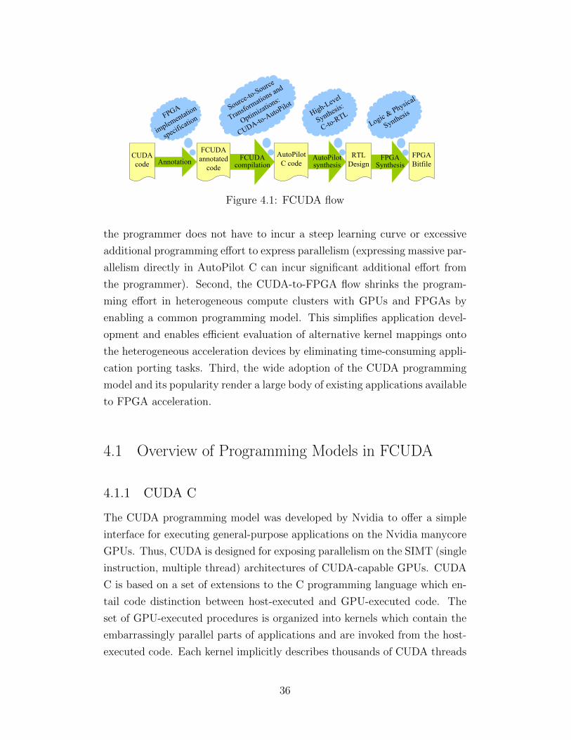
AnnotationFCUDAannotated
codeFCUDA
compilationAutoPilot
C codeAutoPilotsynthesis
RTLDesign
FPGA
implementation
specification
Source-to-Source
Transformations and
Optimizations:
CUDA-to-AutoPilotHigh-Level
Synthesis:
C-to-RTL
FPGA Synthesis
FPGABitfile
Logic & Physical
Synthesis
CUDA code
Figure 4.1: FCUDA flow
the programmer does not have to incur a steep learning curve or excessive
additional programming effort to express parallelism (expressing massive par-
allelism directly in AutoPilot C can incur significant additional effort from
the programmer). Second, the CUDA-to-FPGA flow shrinks the program-
ming effort in heterogeneous compute clusters with GPUs and FPGAs by
enabling a common programming model. This simplifies application devel-
opment and enables efficient evaluation of alternative kernel mappings onto
the heterogeneous acceleration devices by eliminating time-consuming appli-
cation porting tasks. Third, the wide adoption of the CUDA programming
model and its popularity render a large body of existing applications available
to FPGA acceleration.
4.1 Overview of Programming Models in FCUDA
4.1.1 CUDA C
The CUDA programming model was developed by Nvidia to offer a simple
interface for executing general-purpose applications on the Nvidia manycore
GPUs. Thus, CUDA is designed for exposing parallelism on the SIMT (single
instruction, multiple thread) architectures of CUDA-capable GPUs. CUDA
C is based on a set of extensions to the C programming language which en-
tail code distinction between host-executed and GPU-executed code. The
set of GPU-executed procedures is organized into kernels which contain the
embarrassingly parallel parts of applications and are invoked from the host-
executed code. Each kernel implicitly describes thousands of CUDA threads
36
that are organized in groups called threadblocks. Threadblocks are further
organized into a grid structure (Figure 4.2). The number of threadblocks
per grid and threads per threadblock are specified in the host code, whereas
built-in variables (i.e. threadIdx, blockIdx) may be used in the kernel to
specify the computation performed by each thread in the SIMT architec-
ture. It is the programmer’s responsibility to partition the computation into
parallel coarse-grained tasks (threadblocks) that consist of finer-grained sub-
tasks (threads) that can execute in parallel. The proposed FCUDA frame-
work maps the dual-granularity parallelism contained in the hierarchy of
threads and threadblocks of the kernel onto spatial hardware parallelism on
the FPGA.
CUDA extends C with synchronization directives that control how threads
within a threadblock execute with respect to each other (i.e. synchronization
points impose a bulk-synchronous type of parallelism). Conversely, thread-
blocks are designed to execute independently in any parallel or sequential
fashion without side-effects in the execution correctness. In recent updates
of the CUDA platform, atomic operations and fence directives can be used
to enforce the order of memory accesses either at the threadblock or the grid
level. The two granularities of CUDA parallelism are also represented in the
SIMT architecture (Figure 4.2), where streaming processors (SPs) are clus-
tered in streaming multiprocessors (SMs). Each threadblock is assigned to
one SM and its corresponding threads are executed on the SPs of the SM in a
sequence of bundles, called warps. The SIMT architecture executes warps in
a SIMD (single instruction, multiple data) fashion when warp threads con-
verge on the same control flow. On the other hand, control flow divergent
threads within a warp execute sequentially, limiting the amount of exploited
concurrency from the SIMT hardware. The FCUDA framework generates
threadblock customized processing engines (PEs) with custom thread-level
parallelism, as specified by the programmer and performance-resource budget
tradeoffs.
The CUDA programming model entails multiple memory spaces with di-
verse characteristics. In terms of visibility, memory spaces can be distin-
guished into thread-private (e.g. SP-allocated registers), threadblock-private
(e.g. SM-coupled on-chip memory) and global (e.g. off-chip DDR mem-
ory). Each SP is allocated a set of registers out of a pool of SM registers
according to the kernel’s variable use. The SM-coupled memory is called
37
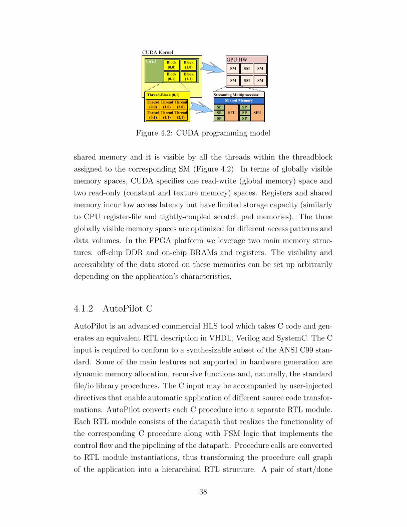
CUDA Kernel
Grid Block(0,0)
Block(1,0)
Block(0,1)
Block(1,1)
Thread-Block (0,1)
Thread(0,0)
Thread(1,0)
Thread(2,0)
Thread(0,1)
Thread(1,1)
Thread(2,1)
GPU HWSM SM SM
SM SM SM
Streaming MultiprocessorShared Memory
SPSPSP
SPSPSP
SFU SFU
Figure 4.2: CUDA programming model
shared memory and it is visible by all the threads within the threadblock
assigned to the corresponding SM (Figure 4.2). In terms of globally visible
memory spaces, CUDA specifies one read-write (global memory) space and
two read-only (constant and texture memory) spaces. Registers and shared
memory incur low access latency but have limited storage capacity (similarly
to CPU register-file and tightly-coupled scratch pad memories). The three
globally visible memory spaces are optimized for different access patterns and
data volumes. In the FPGA platform we leverage two main memory struc-
tures: off-chip DDR and on-chip BRAMs and registers. The visibility and
accessibility of the data stored on these memories can be set up arbitrarily
depending on the application’s characteristics.
4.1.2 AutoPilot C
AutoPilot is an advanced commercial HLS tool which takes C code and gen-
erates an equivalent RTL description in VHDL, Verilog and SystemC. The C
input is required to conform to a synthesizable subset of the ANSI C99 stan-
dard. Some of the main features not supported in hardware generation are
dynamic memory allocation, recursive functions and, naturally, the standard
file/io library procedures. The C input may be accompanied by user-injected
directives that enable automatic application of different source code transfor-
mations. AutoPilot converts each C procedure into a separate RTL module.
Each RTL module consists of the datapath that realizes the functionality of
the corresponding C procedure along with FSM logic that implements the
control flow and the pipelining of the datapath. Procedure calls are converted
to RTL module instantiations, thus transforming the procedure call graph
of the application into a hierarchical RTL structure. A pair of start/done
38
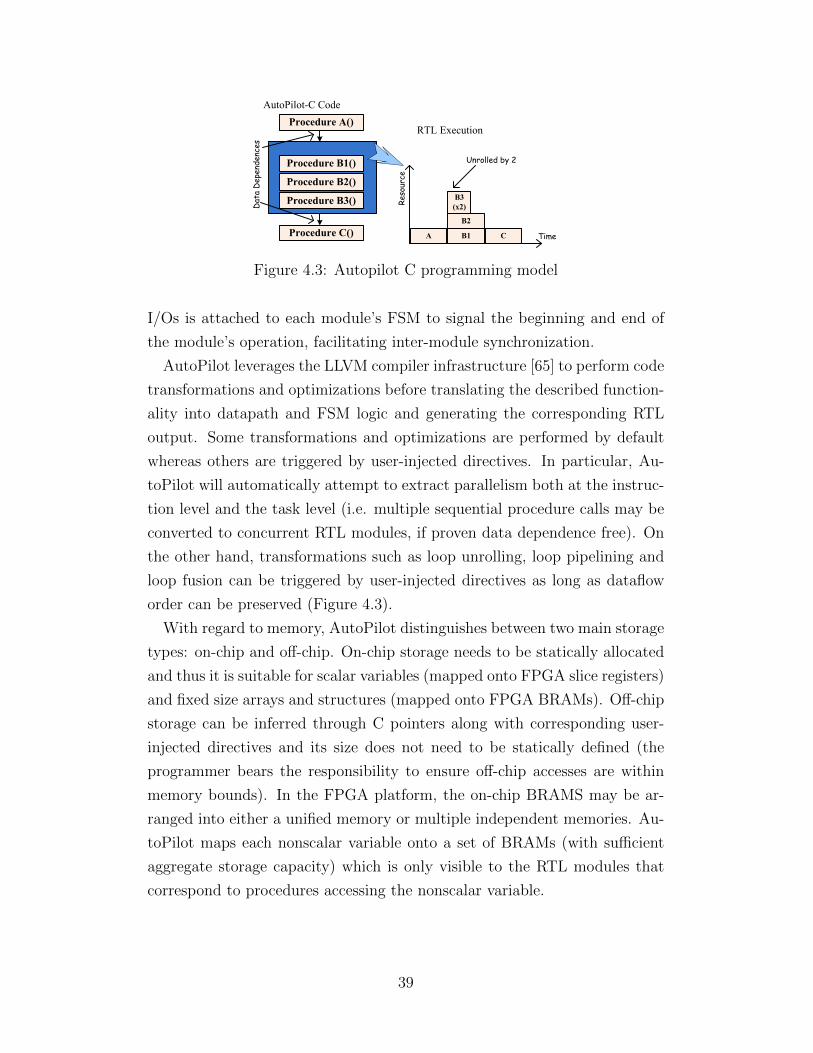
AutoPilot-C Code
Procedure B1()
Procedure B2()
Procedure B3()
Procedure A()
Procedure C() A
Dat
a D
epen
denc
es
RTL Execution
Time
Reso
urce
B1
B2
B3 (x2)
C
Unrolled by 2
Figure 4.3: Autopilot C programming model
I/Os is attached to each module’s FSM to signal the beginning and end of
the module’s operation, facilitating inter-module synchronization.
AutoPilot leverages the LLVM compiler infrastructure [65] to perform code
transformations and optimizations before translating the described function-
ality into datapath and FSM logic and generating the corresponding RTL
output. Some transformations and optimizations are performed by default
whereas others are triggered by user-injected directives. In particular, Au-
toPilot will automatically attempt to extract parallelism both at the instruc-
tion level and the task level (i.e. multiple sequential procedure calls may be
converted to concurrent RTL modules, if proven data dependence free). On
the other hand, transformations such as loop unrolling, loop pipelining and
loop fusion can be triggered by user-injected directives as long as dataflow
order can be preserved (Figure 4.3).
With regard to memory, AutoPilot distinguishes between two main storage
types: on-chip and off-chip. On-chip storage needs to be statically allocated
and thus it is suitable for scalar variables (mapped onto FPGA slice registers)
and fixed size arrays and structures (mapped onto FPGA BRAMs). Off-chip
storage can be inferred through C pointers along with corresponding user-
injected directives and its size does not need to be statically defined (the
programmer bears the responsibility to ensure off-chip accesses are within
memory bounds). In the FPGA platform, the on-chip BRAMS may be ar-
ranged into either a unified memory or multiple independent memories. Au-
toPilot maps each nonscalar variable onto a set of BRAMs (with sufficient
aggregate storage capacity) which is only visible to the RTL modules that
correspond to procedures accessing the nonscalar variable.
39
4.1.3 Programming-Model Translation Advantages
As compute infrastructure becomes increasingly heterogeneous with differ-
ent types of parallel processing accelerators, FCUDA is essentially offering
an inter-programming-model translation tool for efficient kernel portability
across GPUs and FPGAs. In this work we facilitate translation of CUDA
C into AutoPilot C. However, the proposed techniques can be applied in
the translation of alternative parallel programming models (e.g. OpenCL).
Moreover, alternative HLS tools with different coarse-grained parallelism se-
mantics in their programming models can be considered in similar frame-
works.
The current implementation of FCUDA combines the advantages of the
CUDA programming model with the advanced high-level synthesis infras-
tructure of AutoPilot. The CUDA C programming model provides high
abstraction and incurs a low learning curve while enabling parallelism expres-
sion in a very concise manner (i.e. enables higher programming productivity
compared to AutoPilot C). FCUDA uses source-to-source transformations
and optimizations to convert the CUDA threadblock and thread parallelism
into procedure and loop iteration parallelism in AutoPilot’s C programming
model. By leveraging high-level source-to-source transformations rather than
low level IR translation (e.g. from CUDA’s assembly-like PTX IR to RTL),
FCUDA can efficiently exploit different levels of coarse-grained parallelism
while leveraging existing HLS infrastructures. Furthermore, an important
benefit of leveraging CUDA for FPGA programming is the distinction of on-
chip and off-chip memory spaces in the CUDA C programming model. This
fits well with the memory view within hardware synthesis flows. The trans-
formations entailed in FCUDA automate the cumbersome task of replication
and interconnection of parallel processing engines (PEs) along with their
associated on-chip memory buffers and the data transfers from/to off-chip
memories.
4.2 FCUDA Framework
The CUDA-to-FPGA flow of FCUDA (Figure 4.1) is based on a source-to-
source transformation and optimization (SSTO) engine which implements
two main types of code transformations: (i) dataflow and compute opti-
40
mizations (DCO) and (ii) parallelism translation transformations (PTT).
The dataflow and compute optimizations are based on analysis of the kernel
dataflow followed by data communication and computation re-organization.
These optimizations facilitate efficient fitting of the kernel computation and
data communication onto the FPGA hardware. The parallelism transla-
tion transformations leverage the kernel inherent parallelism by mapping it
into AutoPilot C coarse-granularity parallel structures. Some of these trans-
formations are applicable to all of the kernels, while others are triggered
by code-injected pragmas which specify their application parameters. The
FCUDA SSTO engine has been implemented using the Cetus [66] paralleliz-
ing compiler infrastructure.
After FCUDA compilation, AutoPilot extracts fine-grained instruction-
level parallelism from the transformed code and pipelines the design accord-
ing to the user-specified clock period using its SDC-based scheduling engine
[31]. Moreover, it identifies and leverages parallel constructs in the input
code to generate coarse-grained concurrency in the RTL output. The flow
(Figure 4.1) is completed by leveraging the Xilinx FPGA synthesis and phys-
ical implementation tools to map the generated RTL onto the reconfigurable
fabric. In the following subsections we discuss the philosophy of the FCUDA
translation and present an overview of the transformation algorithm followed
by a description of the FCUDA pragmas leveraged in the framework to guide
the translation process.
4.2.1 CUDA-C to Autopilot-C Translation Philosophy
The FCUDA framework takes advantage of the abundant spatial parallelism
available on the reconfigurable logic to accelerate massively parallel com-
putations described in CUDA C. Thus, mapping application coarse-grained
parallelism on hardware is important in achieving high performance. In the
CUDA programming model, coarse-grained parallelism is organized in two
levels of granularity: threads and threadblocks (Figure 4.2). As mentioned
earlier, the FCUDA SSTO engine maps the CUDA coarse-grained paral-
lelism into loop- and procedure-level parallelism. Listings 4.1–4.3 offer some
insight into how this is achieved for the CP CUDA kernel. Listing 4.1 depicts
the kernel code expressed in the CUDA programming model. As mentioned
41
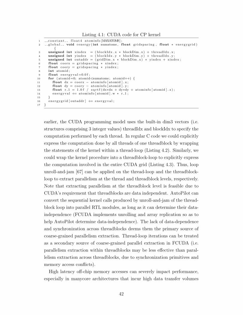
Listing 4.1: CUDA code for CP kernel1 c o n s t a n t f l o a t 4 atominfo [MAXATOMS] ;2 g l o b a l void cenergy ( int numatoms , f loat gr idspac ing , f loat ∗ energygr id )
{3 unsigned int xindex = ( blockIdx . x ∗ blockDim . x ) + threadIdx . x ;4 unsigned int yindex = ( blockIdx . y ∗ blockDim . y ) + threadIdx . y ;5 unsigned int outaddr = ( gridDim . x ∗ blockDim . x ) ∗ yindex + xindex ;6 f loat coorx = gr id spac ing ∗ xindex ;7 f loat coory = gr id spac ing ∗ yindex ;8 int atomid ;9 f loat energyva l =0.0 f ;
10 for ( atomid=0; atomid<numatoms ; atomid++) {11 f loat dx = coorx − atominfo [ atomid ] . x ;12 f loat dy = coory − atominfo [ atomid ] . y ;13 f loat r 1 = 1 .0 f / s q r t f ( dx∗dx + dy∗dy + atominfo [ atomid ] . z ) ;14 energyva l += atominfo [ atomid ] .w ∗ r 1 ;15 }16 energygr id [ outaddr ] += energyva l ;17 }
earlier, the CUDA programming model uses the built-in dim3 vectors (i.e.
structures comprising 3 integer values) threadIdx and blockIdx to specify the
computation performed by each thread. In regular C code we could explicitly
express the computation done by all threads of one threadblock by wrapping
the statements of the kernel within a thread-loop (Listing 4.2). Similarly, we
could wrap the kernel procedure into a threadblock-loop to explicitly express
the computation involved in the entire CUDA grid (Listing 4.3). Thus, loop
unroll-and-jam [67] can be applied on the thread-loop and the threadblock-
loop to extract parallelism at the thread and threadblock levels, respectively.
Note that extracting parallelism at the threadblock level is feasible due to
CUDA’s requirement that threadblocks are data independent. AutoPilot can
convert the sequential kernel calls produced by unroll-and-jam of the thread-
block loop into parallel RTL modules, as long as it can determine their data-
independence (FCUDA implements unrolling and array replication so as to
help AutoPilot determine data-independence). The lack of data-dependence
and synchronization across threadblocks deems them the primary source of
coarse-grained parallelism extraction. Thread-loop iterations can be treated
as a secondary source of coarse-grained parallel extraction in FCUDA (i.e.
parallelism extraction within threadblocks may be less effective than paral-
lelism extraction across threadblocks, due to synchronization primitives and
memory access conflicts).
High latency off-chip memory accesses can severely impact performance,
especially in manycore architectures that incur high data transfer volumes
42
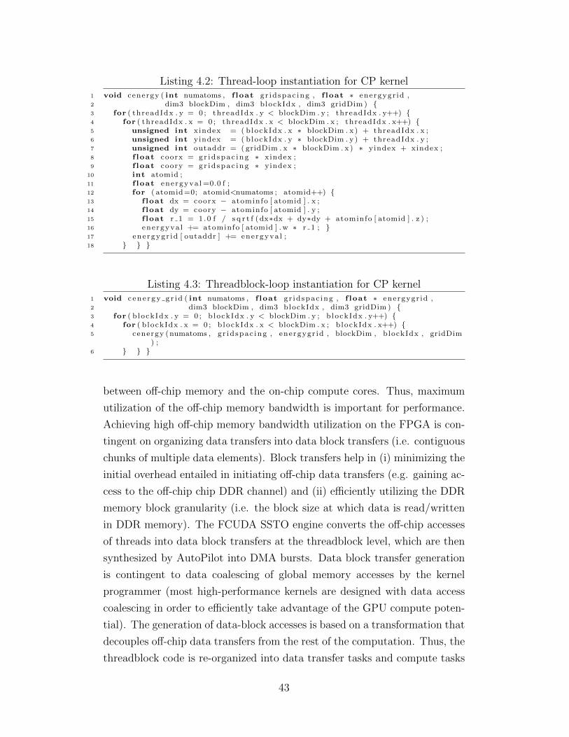
Listing 4.2: Thread-loop instantiation for CP kernel1 void cenergy ( int numatoms , f loat gr idspac ing , f loat ∗ energygr id ,2 dim3 blockDim , dim3 blockIdx , dim3 gridDim ) {3 for ( threadIdx . y = 0 ; threadIdx . y < blockDim . y ; threadIdx . y++) {4 for ( threadIdx . x = 0 ; threadIdx . x < blockDim . x ; threadIdx . x++) {5 unsigned int xindex = ( blockIdx . x ∗ blockDim . x ) + threadIdx . x ;6 unsigned int yindex = ( blockIdx . y ∗ blockDim . y ) + threadIdx . y ;7 unsigned int outaddr = ( gridDim . x ∗ blockDim . x ) ∗ yindex + xindex ;8 f loat coorx = gr id spac ing ∗ xindex ;9 f loat coory = gr id spac ing ∗ yindex ;
10 int atomid ;11 f loat energyva l =0.0 f ;12 for ( atomid=0; atomid<numatoms ; atomid++) {13 f loat dx = coorx − atominfo [ atomid ] . x ;14 f loat dy = coory − atominfo [ atomid ] . y ;15 f loat r 1 = 1 .0 f / s q r t f ( dx∗dx + dy∗dy + atominfo [ atomid ] . z ) ;16 energyva l += atominfo [ atomid ] .w ∗ r 1 ; }17 energygr id [ outaddr ] += energyva l ;18 } } }
Listing 4.3: Threadblock-loop instantiation for CP kernel1 void c ene rgy g r i d ( int numatoms , f loat gr idspac ing , f loat ∗ energygr id ,2 dim3 blockDim , dim3 blockIdx , dim3 gridDim ) {3 for ( b lockIdx . y = 0 ; b lockIdx . y < blockDim . y ; b lockIdx . y++) {4 for ( b lockIdx . x = 0 ; b lockIdx . x < blockDim . x ; b lockIdx . x++) {5 cenergy (numatoms , gr id spac ing , energygr id , blockDim , blockIdx , gridDim
) ;6 } } }
between off-chip memory and the on-chip compute cores. Thus, maximum
utilization of the off-chip memory bandwidth is important for performance.
Achieving high off-chip memory bandwidth utilization on the FPGA is con-
tingent on organizing data transfers into data block transfers (i.e. contiguous
chunks of multiple data elements). Block transfers help in (i) minimizing the
initial overhead entailed in initiating off-chip data transfers (e.g. gaining ac-
cess to the off-chip chip DDR channel) and (ii) efficiently utilizing the DDR
memory block granularity (i.e. the block size at which data is read/written
in DDR memory). The FCUDA SSTO engine converts the off-chip accesses
of threads into data block transfers at the threadblock level, which are then
synthesized by AutoPilot into DMA bursts. Data block transfer generation
is contingent to data coalescing of global memory accesses by the kernel
programmer (most high-performance kernels are designed with data access
coalescing in order to efficiently take advantage of the GPU compute poten-
tial). The generation of data-block accesses is based on a transformation that
decouples off-chip data transfers from the rest of the computation. Thus, the
threadblock code is re-organized into data transfer tasks and compute tasks
43
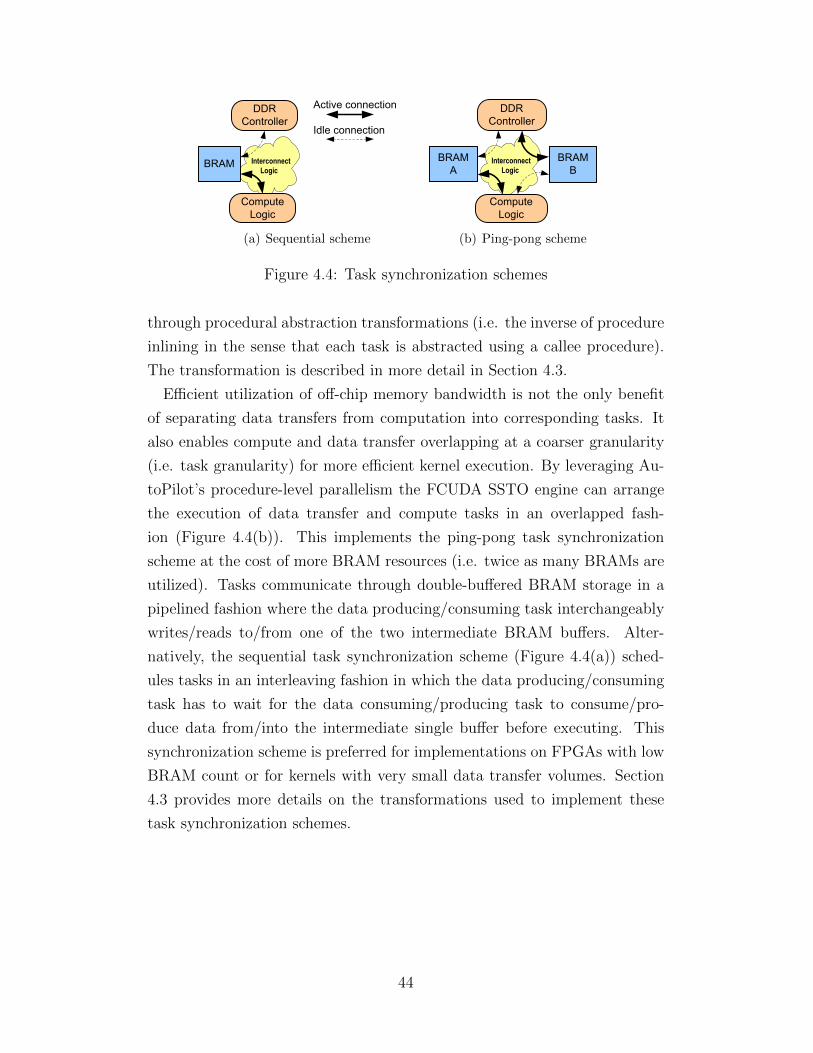
InterconnectLogic
BRAM
DDR Controller
Compute Logic
Active connection
Idle connection
(a) Sequential scheme
InterconnectLogic
BRAM A
DDR Controller
Compute Logic
BRAM B
(b) Ping-pong scheme
Figure 4.4: Task synchronization schemes
through procedural abstraction transformations (i.e. the inverse of procedure
inlining in the sense that each task is abstracted using a callee procedure).
The transformation is described in more detail in Section 4.3.
Efficient utilization of off-chip memory bandwidth is not the only benefit
of separating data transfers from computation into corresponding tasks. It
also enables compute and data transfer overlapping at a coarser granularity
(i.e. task granularity) for more efficient kernel execution. By leveraging Au-
toPilot’s procedure-level parallelism the FCUDA SSTO engine can arrange
the execution of data transfer and compute tasks in an overlapped fash-
ion (Figure 4.4(b)). This implements the ping-pong task synchronization
scheme at the cost of more BRAM resources (i.e. twice as many BRAMs are
utilized). Tasks communicate through double-buffered BRAM storage in a
pipelined fashion where the data producing/consuming task interchangeably
writes/reads to/from one of the two intermediate BRAM buffers. Alter-
natively, the sequential task synchronization scheme (Figure 4.4(a)) sched-
ules tasks in an interleaving fashion in which the data producing/consuming
task has to wait for the data consuming/producing task to consume/pro-
duce data from/into the intermediate single buffer before executing. This
synchronization scheme is preferred for implementations on FPGAs with low
BRAM count or for kernels with very small data transfer volumes. Section
4.3 provides more details on the transformations used to implement these
task synchronization schemes.
44
4.2.2 FCUDA Compilation Overview
The translation flow from CUDA-C to AutoPilot-C is based on a sequence of
DCO and PTT passes which are applied to each CUDA kernel. A high-level
overview of the FCUDA pass sequence is depicted in Algorithm 4.1. The first
two passes, constantMemoryStreaming() and globalMemoryBuffering(),
handle mapping of CUDA memory spaces onto on-chip BRAM buffers. The
constantMemoryStreaming() pass allocates BRAMs for buffering constant
memory arrays along with setting up constant data streaming to the allo-
cated constant memory buffers. Thus, it helps eliminate multiple kernel in-
vocations. The globalMemoryBuffering() pass, on the other hand, allocates
BRAMs for global memory data stored in shared memory arrays or registers
blocks. Both of the BRAM allocation passes are described in more depth in
Section 4.3.1.
Subsequently, createKernelTasks() splits the kernel into data-transfer and
compute tasks. This pass entails common-subexpression-elimination (CSE)
and code motion optimizations [67], along with task abstraction (i.e. pro-
cedural abstraction of tasks) transformations (Section 4.3.2). Thread-loop
generation and unrolling are implemented by createThreadLoop() and un-
rollThreadLoop() passes, respectively. The degree of thread-loop unrolling
is specified through an FCUDA directive (see Section 4.2.3). The program-
mer can specify a unit unroll degree to prevent thread-loop unrolling. The
array-partitioning pass, partitionArrays(), helps eliminate the BRAM ac-
cess performance bottleneck that unrolling may incur (degree of partitioning
specified through FCUDA directive).
The following three passes in lines 8–10 of Algorithm 4.1 leverage the
coarse-grained parallelism at the threadblock level. The createThreadblock-
Loop() transformation pass wraps the kernel code with a threadblock-loop,
while pass unrollThreadblockLoop() unrolls the threadblock-loop by the de-
gree specified in a corresponding FCUDA directive (see Section 4.2.3). In-
between these two passes, buildTaskSynchronization() sets up the task syn-
chronization scheme (sequential or ping-pong) across tasks.
The CUDA programming model contains thread-synchronization primi-
tives that can be used by the programmer to eliminate data races and
dependences within a threadblock (e.g.__syncthreads()). Representation
of CUDA threads as thread-loops in AutoPilot-C (Listing 4.2) may break
45
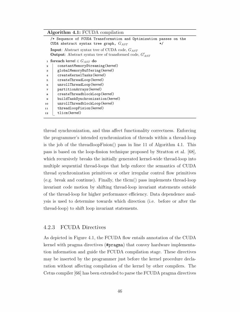
Algorithm 4.1: FCUDA compilation
/* Sequence of FCUDA Transformation and Optimization passes on the
CUDA abstract syntax tree graph, GAST */
Input: Abstract syntax tree of CUDA code, GAST
Output: Abstract syntax tree of transformed code, G′AST
1 foreach kernel ∈ GAST do2 constantMemoryStreaming(kernel)3 globalMemoryBuffering(kernel)4 createKernelTasks(kernel)5 createThreadLoop(kernel)6 unrollThreadLoop(kernel)7 partitionArrays(kernel)8 createThreadblockLoop(kernel)9 buildTaskSynchronization(kernel)
10 unrollThreadblockLoop(kernel)11 threadloopFision(kernel)12 tlicm(kernel)
thread synchronization, and thus affect functionality correctness. Enforcing
the programmer’s intended synchronization of threads within a thread-loop
is the job of the threadloopFision() pass in line 11 of Algorithm 4.1. This
pass is based on the loop-fission technique proposed by Stratton et al. [68],
which recursively breaks the initially generated kernel-wide thread-loop into
multiple sequential thread-loops that help enforce the semantics of CUDA
thread synchronization primitives or other irregular control flow primitives
(e.g. break and continue). Finally, the tlicm() pass implements thread-loop
invariant code motion by shifting thread-loop invariant statements outside
of the thread-loop for higher performance efficiency. Data dependence anal-
ysis is used to determine towards which direction (i.e. before or after the
thread-loop) to shift loop invariant statements.
4.2.3 FCUDA Directives
As depicted in Figure 4.1, the FCUDA flow entails annotation of the CUDA
kernel with pragma directives (#pragma) that convey hardware implementa-
tion information and guide the FCUDA compilation stage. These directives
may be inserted by the programmer just before the kernel procedure decla-
ration without affecting compilation of the kernel by other compilers. The
Cetus compiler [66] has been extended to parse the FCUDA pragma directives
46
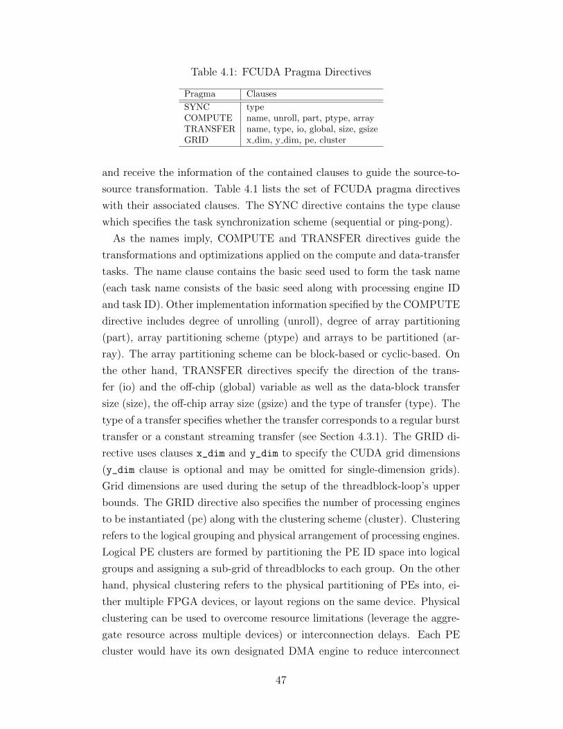
Table 4.1: FCUDA Pragma Directives
Pragma Clauses
SYNC typeCOMPUTE name, unroll, part, ptype, arrayTRANSFER name, type, io, global, size, gsizeGRID x dim, y dim, pe, cluster
and receive the information of the contained clauses to guide the source-to-
source transformation. Table 4.1 lists the set of FCUDA pragma directives
with their associated clauses. The SYNC directive contains the type clause
which specifies the task synchronization scheme (sequential or ping-pong).
As the names imply, COMPUTE and TRANSFER directives guide the
transformations and optimizations applied on the compute and data-transfer
tasks. The name clause contains the basic seed used to form the task name
(each task name consists of the basic seed along with processing engine ID
and task ID). Other implementation information specified by the COMPUTE
directive includes degree of unrolling (unroll), degree of array partitioning
(part), array partitioning scheme (ptype) and arrays to be partitioned (ar-
ray). The array partitioning scheme can be block-based or cyclic-based. On
the other hand, TRANSFER directives specify the direction of the trans-
fer (io) and the off-chip (global) variable as well as the data-block transfer
size (size), the off-chip array size (gsize) and the type of transfer (type). The
type of a transfer specifies whether the transfer corresponds to a regular burst
transfer or a constant streaming transfer (see Section 4.3.1). The GRID di-
rective uses clauses x_dim and y_dim to specify the CUDA grid dimensions
(y_dim clause is optional and may be omitted for single-dimension grids).
Grid dimensions are used during the setup of the threadblock-loop’s upper
bounds. The GRID directive also specifies the number of processing engines
to be instantiated (pe) along with the clustering scheme (cluster). Clustering
refers to the logical grouping and physical arrangement of processing engines.
Logical PE clusters are formed by partitioning the PE ID space into logical
groups and assigning a sub-grid of threadblocks to each group. On the other
hand, physical clustering refers to the physical partitioning of PEs into, ei-
ther multiple FPGA devices, or layout regions on the same device. Physical
clustering can be used to overcome resource limitations (leverage the aggre-
gate resource across multiple devices) or interconnection delays. Each PE
cluster would have its own designated DMA engine to reduce interconnect
47
delay. This also enables more efficient data communication schemes across
PE clusters, such as pipelined busses or on-chip networks. These schemes
incur a resource penalty, which can be better leveraged at the cluster level
rather than the PE level.
4.3 Transformations and Optimizations in FCUDA
Compilation
FCUDA compilation consists of a sequence of source-to-source transforma-
tions and optimizations that convert the input CUDA-C code to AutoPilot-C
code with explicit procedure and loop-level parallelism that AutoPilot can
map into parallel hardware logic. Leveraging parallelizing transformations at
the source code level can be more effective than at lower intermediate repre-
sentations (e.g. CUDA PTX or LLVM IR) that decompose the code in much
finer operations and tasks. In this section we discuss in more detail some of
the transformations and optimization involved in the FCUDA compilation
flow.
4.3.1 CUDA Memory Space Mapping
As discussed in Section 4.1.2, CUDA leverages five different memory spaces:
(i) registers, (ii) shared memory, (iii) global memory, (iv) constant memory
and (v) texture memory. Each memory space has different attributes and ac-
cess latency characteristics which affect its usage scenarios and consequently
affect how they are leveraged in FCUDA (texture memory is not currently
supported in the FCUDA framework).
CUDA Constant Memory
Constant memory is used to store read-only variables that are visible to
all threadblocks. In the CUDA architecture a small portion of the off-chip
memory is reserved as constant memory, whereas SM-private caches help hide
the latency of constant memory accesses through access patterns with high
spatial and temporal localities. We leverage these attributes in handling con-
stant memory variables according to the compute/data-transfer task decou-
48
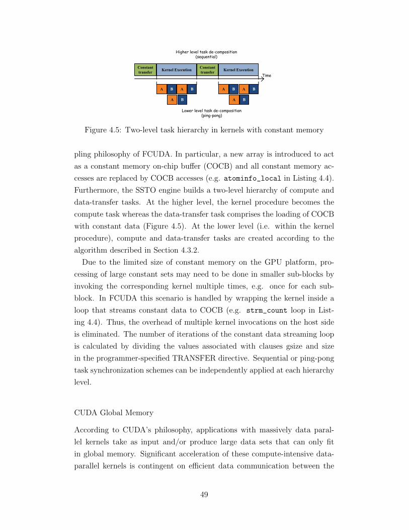
Constant transfer
TimeKernel Execution Constant
transfer
Higher level task de-composition (sequential)
A B
Lower level task de-composition (ping-pong)
A B
A B
Kernel Execution
A B
A B
A B
Figure 4.5: Two-level task hierarchy in kernels with constant memory
pling philosophy of FCUDA. In particular, a new array is introduced to act
as a constant memory on-chip buffer (COCB) and all constant memory ac-
cesses are replaced by COCB accesses (e.g. atominfo_local in Listing 4.4).
Furthermore, the SSTO engine builds a two-level hierarchy of compute and
data-transfer tasks. At the higher level, the kernel procedure becomes the
compute task whereas the data-transfer task comprises the loading of COCB
with constant data (Figure 4.5). At the lower level (i.e. within the kernel
procedure), compute and data-transfer tasks are created according to the
algorithm described in Section 4.3.2.
Due to the limited size of constant memory on the GPU platform, pro-
cessing of large constant sets may need to be done in smaller sub-blocks by
invoking the corresponding kernel multiple times, e.g. once for each sub-
block. In FCUDA this scenario is handled by wrapping the kernel inside a
loop that streams constant data to COCB (e.g. strm_count loop in List-
ing 4.4). Thus, the overhead of multiple kernel invocations on the host side
is eliminated. The number of iterations of the constant data streaming loop
is calculated by dividing the values associated with clauses gsize and size
in the programmer-specified TRANSFER directive. Sequential or ping-pong
task synchronization schemes can be independently applied at each hierarchy
level.
CUDA Global Memory
According to CUDA’s philosophy, applications with massively data paral-
lel kernels take as input and/or produce large data sets that can only fit
in global memory. Significant acceleration of these compute-intensive data-
parallel kernels is contingent on efficient data communication between the
49
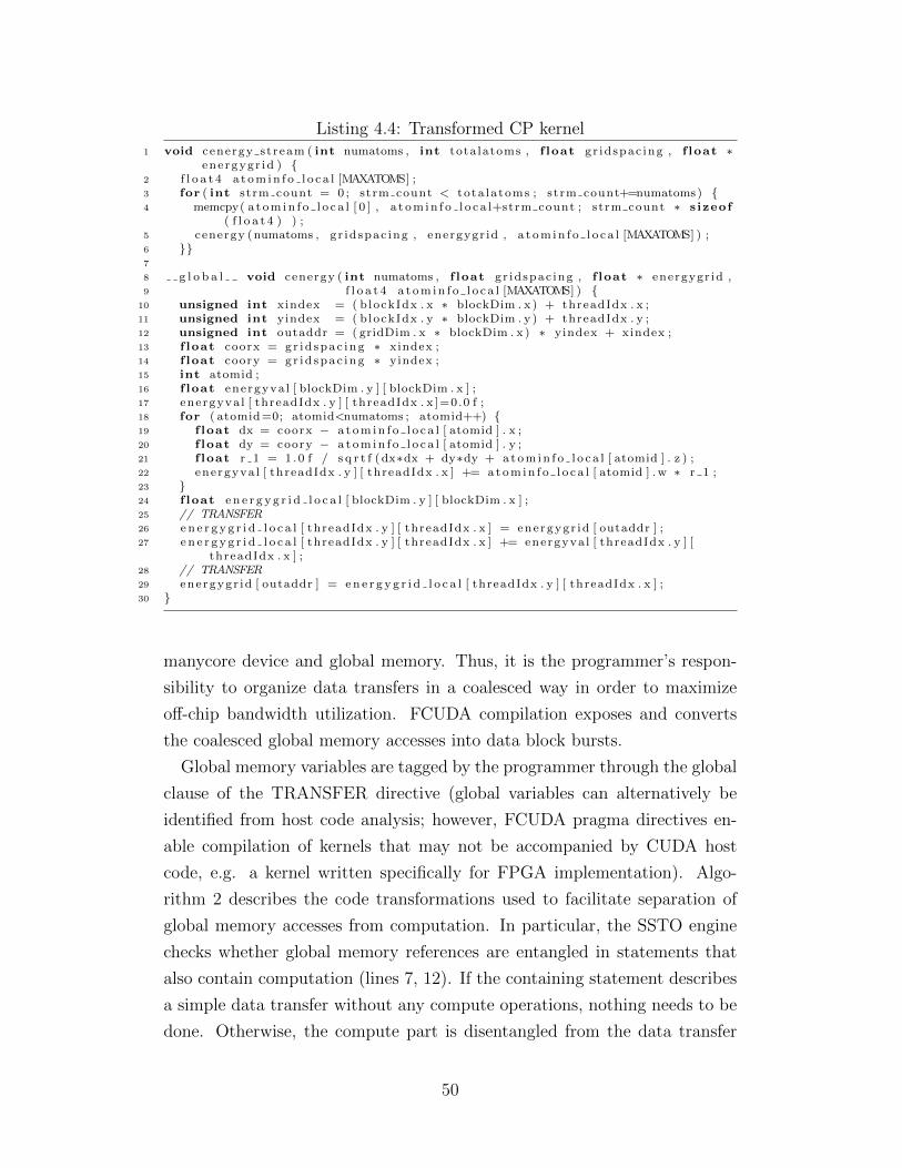
Listing 4.4: Transformed CP kernel1 void cenergy stream ( int numatoms , int totalatoms , f loat gr idspac ing , f loat ∗
energygr id ) {2 f l o a t 4 a t om in f o l o c a l [MAXATOMS] ;3 for ( int strm count = 0 ; strm count < tota latoms ; strm count+=numatoms) {4 memcpy( a t om in f o l o c a l [ 0 ] , a t om in f o l o c a l+strm count ; strm count ∗ s izeof
( f l o a t 4 ) ) ;5 cenergy (numatoms , gr id spac ing , energygr id , a t om in f o l o c a l [MAXATOMS] ) ;6 }}7
8 g l o b a l void cenergy ( int numatoms , f loat gr idspac ing , f loat ∗ energygr id ,9 f l o a t 4 a t om in f o l o c a l [MAXATOMS] ) {
10 unsigned int xindex = ( blockIdx . x ∗ blockDim . x ) + threadIdx . x ;11 unsigned int yindex = ( blockIdx . y ∗ blockDim . y ) + threadIdx . y ;12 unsigned int outaddr = ( gridDim . x ∗ blockDim . x ) ∗ yindex + xindex ;13 f loat coorx = gr id spac ing ∗ xindex ;14 f loat coory = gr id spac ing ∗ yindex ;15 int atomid ;16 f loat energyva l [ blockDim . y ] [ blockDim . x ] ;17 energyva l [ threadIdx . y ] [ threadIdx . x ]=0.0 f ;18 for ( atomid=0; atomid<numatoms ; atomid++) {19 f loat dx = coorx − a t om in f o l o c a l [ atomid ] . x ;20 f loat dy = coory − a t om in f o l o c a l [ atomid ] . y ;21 f loat r 1 = 1 .0 f / s q r t f ( dx∗dx + dy∗dy + atom in f o l o c a l [ atomid ] . z ) ;22 energyva l [ threadIdx . y ] [ threadIdx . x ] += atom in f o l o c a l [ atomid ] .w ∗ r 1 ;23 }24 f loat e n e r g y g r i d l o c a l [ blockDim . y ] [ blockDim . x ] ;25 // TRANSFER26 e n e r g y g r i d l o c a l [ threadIdx . y ] [ threadIdx . x ] = energygr id [ outaddr ] ;27 e n e r g y g r i d l o c a l [ threadIdx . y ] [ threadIdx . x ] += energyva l [ threadIdx . y ] [
threadIdx . x ] ;28 // TRANSFER29 energygr id [ outaddr ] = en e r g y g r i d l o c a l [ threadIdx . y ] [ threadIdx . x ] ;30 }
manycore device and global memory. Thus, it is the programmer’s respon-
sibility to organize data transfers in a coalesced way in order to maximize
off-chip bandwidth utilization. FCUDA compilation exposes and converts
the coalesced global memory accesses into data block bursts.
Global memory variables are tagged by the programmer through the global
clause of the TRANSFER directive (global variables can alternatively be
identified from host code analysis; however, FCUDA pragma directives en-
able compilation of kernels that may not be accompanied by CUDA host
code, e.g. a kernel written specifically for FPGA implementation). Algo-
rithm 2 describes the code transformations used to facilitate separation of
global memory accesses from computation. In particular, the SSTO engine
checks whether global memory references are entangled in statements that
also contain computation (lines 7, 12). If the containing statement describes
a simple data transfer without any compute operations, nothing needs to be
done. Otherwise, the compute part is disentangled from the data transfer
50
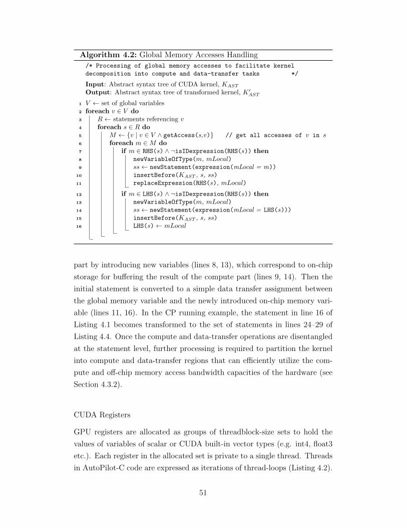
Algorithm 4.2: Global Memory Accesses Handling
/* Processing of global memory accesses to facilitate kernel
decomposition into compute and data-transfer tasks */
Input: Abstract syntax tree of CUDA kernel, KAST
Output: Abstract syntax tree of transformed kernel, K ′AST
1 V ← set of global variables2 foreach v ∈ V do3 R← statements referencing v4 foreach s ∈ R do5 M ← {v | v ∈ V ∧ getAccess(s,v)} // get all accesses of v in s6 foreach m ∈M do7 if m ∈ RHS(s) ∧ ¬isIDexpression(RHS(s)) then8 newVariableOfType(m, mLocal)9 ss← newStatement(expression(mLocal = m))
10 insertBefore(KAST , s, ss)11 replaceExpression(RHS(s), mLocal)
12 if m ∈ LHS(s) ∧ ¬isIDexpression(RHS(s)) then13 newVariableOfType(m, mLocal)14 ss← newStatement(expression(mLocal = LHS(s)))15 insertBefore(KAST , s, ss)16 LHS(s)← mLocal
part by introducing new variables (lines 8, 13), which correspond to on-chip
storage for buffering the result of the compute part (lines 9, 14). Then the
initial statement is converted to a simple data transfer assignment between
the global memory variable and the newly introduced on-chip memory vari-
able (lines 11, 16). In the CP running example, the statement in line 16 of
Listing 4.1 becomes transformed to the set of statements in lines 24–29 of
Listing 4.4. Once the compute and data-transfer operations are disentangled
at the statement level, further processing is required to partition the kernel
into compute and data-transfer regions that can efficiently utilize the com-
pute and off-chip memory access bandwidth capacities of the hardware (see
Section 4.3.2).
CUDA Registers
GPU registers are allocated as groups of threadblock-size sets to hold the
values of variables of scalar or CUDA built-in vector types (e.g. int4, float3
etc.). Each register in the allocated set is private to a single thread. Threads
in AutoPilot-C code are expressed as iterations of thread-loops (Listing 4.2).
51
Thread serialization in the form of loop iterations creates the opportunity
for register sharing between threads. That is, the FPGA registers allocated
for scalar or vector variables may be re-used across iterations (clearly, in the
case of partial thread-loop unrolling, register sharing may be applied only
across nonconcurrent threads). However, for certain variables, register shar-
ing may not be feasible. This is the case for variables that are live across
CUDA synchronization primitives or FCUDA tasks (i.e. read-after-read and
read-after-write dependent accesses are located in alternate sides of thread
synchronization boundaries). The SSTO engine uses data dependence anal-
ysis to identify and convert such variables into arrays of threadblock dimen-
sionality (e.g. variable energyval in Listing 4.4). Subsequently, AutoPilot
maps them onto BRAMs.
CUDA Shared Memory
Shared memory variables are threadblock private (i.e. only threads within the
corresponding threadblock have visibility and access), and thus can be con-
veniently translated into BRAM-based memories that are accessible only by
the PE executing the corresponding threadblock. Leveraging shared memory
variables in FCUDA comprises (i) replication of the corresponding variable
declaration for each PE referenced in the AutoPilot-C code and (ii) conver-
sion of associated data transfers to/from off-chip memory into DMA bursts.
In terms of access bandwidth, shared memory in GPUs is organized into
banks, allowing multiple (usually 16 in most Nvidia GPUs) concurrent refer-
ences from an equivalent number of parallel threads. In FCUDA parallelism
is primarily and foremost extracted at the threadblock granularity (i.e. par-
allel PEs), whereas thread-level parallelism extraction is less aggressive (i.e
small degrees of thread-loop unrolling are often preferred). Nevertheless, un-
rolling might be useful in cases where threadblock parallelism extraction is
limited by resource or other restrictions. To overcome the performance bot-
tleneck caused by the BRAM port limitation, a pseudo banking technique
is employed. The FCUDA SSTO engine offers an array partitioning trans-
formation (i.e. for arrays accessed using affine expressions of thread-loop
indices), which can be leveraged to increase array access bandwidth by dis-
tributing the generated sub-arrays over multiple BRAMs. Thus, in the case
of thread-loop unrolling, the PE can complete multiple concurrent array ac-
52
cesses. This technique is also applicable to arrays formed by vectorization of
scalar variables.
4.3.2 Kernel Decomposition into Compute and Data-TransferTasks
Having completed handling of the memory accesses (constantMemoryStream-
ing() and globalMemoryBuffering() SSTO passes in Algorithm 4.1) for the
different memory spaces, the kernel compute and data-transfer operations are
disentangled at the statement level (as annotated in Listing 4.4). However,
efficient utilization of the off-chip bandwidth capacity as well as the com-
pute capacity of the device may be constrained by the interleaving between
compute and data-transfer statements (e.g. interleaving created by lever-
aging energygrid off-chip accesses in the CP kernel in Listing 4.4). As dis-
cussed previously, efficient off-chip bandwidth utilization requires high-degree
thread-loop unrolling to convert individual thread data-transfers into block
bursts. On the other hand, unrolling of the compute part of thread-loops
may be feasible (e.g. due to resource constraints) or beneficial (e.g. due to
performance peak) for lower unroll degrees. Moreover, overlapping compute
and data-transfer tasks, through the ping-pong task synchronization scheme,
is usually more efficient across long sequences of statements. Thus, prior to
applying procedural abstraction to create compute and data-transfer tasks,
SSTO createKernelTasks() pass performs code percolation to form compute
and data-transfer statement regions in the kernel. Subsequently, tasks can
be created at the granularity of statement regions.
The code percolation transformation employed in the FCUDA SSTO is
based on code motion of data-transfer statements. In particular, off-chip
memory read statements are percolated toward the top of the control flow
diagram (CFG), whereas write statements are percolated toward the bottom
of the CFG. Both upward and downward statement percolations shift data-
transfer statements until they encounter (i) another data transfer statement,
(ii) a CUDA synchronization directive or (iii) a data-dependent statement.
Upward code percolation is done in forward order of data-transfer statements
in the CFG, whereas downward code percolation is done in reverse order.
Code percolation may shift statements across entire control flow constructs
53
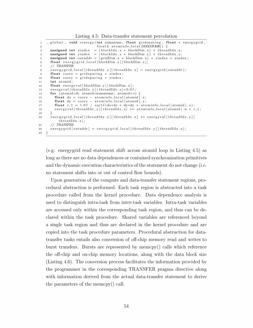
Listing 4.5: Data-transfer statement percolation1 g l o b a l void cenergy ( int numatoms , f loat gr idspac ing , f loat ∗ energygr id ,2 f l o a t 4 a t om in f o l o c a l [MAXATOMS] ) {3 unsigned int xindex = ( blockIdx . x ∗ blockDim . x ) + threadIdx . x ;4 unsigned int yindex = ( blockIdx . y ∗ blockDim . y ) + threadIdx . y ;5 unsigned int outaddr = ( gridDim . x ∗ blockDim . x ) ∗ yindex + xindex ;6 f loat e n e r g y g r i d l o c a l [ blockDim . y ] [ blockDim . x ] ;7 // TRANSFER8 e n e r g y g r i d l o c a l [ threadIdx . y ] [ threadIdx . x ] = energygr id [ outaddr ] ;9 f loat coorx = gr id spac ing ∗ xindex ;
10 f loat coory = gr id spac ing ∗ yindex ;11 int atomid ;12 f loat energyva l [ blockDim . y ] [ blockDim . x ] ;13 energyva l [ threadIdx . y ] [ threadIdx . x ]=0.0 f ;14 for ( atomid=0; atomid<numatoms ; atomid++) {15 f loat dx = coorx − a t om in f o l o c a l [ atomid ] . x ;16 f loat dy = coory − a t om in f o l o c a l [ atomid ] . y ;17 f loat r 1 = 1 .0 f / s q r t f ( dx∗dx + dy∗dy + atom in f o l o c a l [ atomid ] . z ) ;18 energyva l [ threadIdx . y ] [ threadIdx . x ] += atom in f o l o c a l [ atomid ] .w ∗ r 1 ;19 }20 e n e r g y g r i d l o c a l [ threadIdx . y ] [ threadIdx . x ] += energyva l [ threadIdx . y ] [
threadIdx . x ] ;21 // TRANSFER22 energygr id [ outaddr ] = en e r g y g r i d l o c a l [ threadIdx . y ] [ threadIdx . x ] ;23 }
(e.g. energygrid read statement shift across atomid loop in Listing 4.5) as
long as there are no data dependences or contained synchronization primitives
and the dynamic execution characteristics of the statement do not change (i.e.
no statement shifts into or out of control flow bounds).
Upon generation of the compute and data-transfer statement regions, pro-
cedural abstraction is performed. Each task region is abstracted into a task
procedure called from the kernel procedure. Data dependence analysis is
used to distinguish intra-task from inter-task variables. Intra-task variables
are accessed only within the corresponding task region, and thus can be de-
clared within the task procedure. Shared variables are referenced beyond
a single task region and thus are declared in the kernel procedure and are
copied into the task procedure parameters. Procedural abstraction for data-
transfer tasks entails also conversion of off-chip memory read and writes to
burst transfers. Bursts are represented by memcpy() calls which reference
the off-chip and on-chip memory locations, along with the data block size
(Listing 4.6). The conversion process facilitates the information provided by
the programmer in the corresponding TRANSFER pragma directive along
with information derived from the actual data-transfer statement to derive
the parameters of the memcpy() call.
54
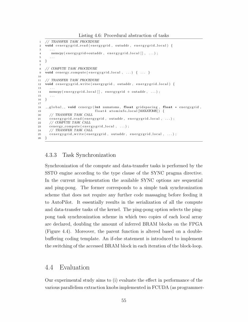
Listing 4.6: Procedural abstraction of tasks1 // TRANSFER TASK PROCEDURE2 void c ene rgyg r id r ead ( energygr id , outaddr , e n e r g y g r i d l o c a l ) {3 . . .4 memcpy( energygr id+outaddr , e n e r g y g r i d l o c a l [ ] , . . . ) ;5 . . .6 }7
8 // COMPUTE TASK PROCEDURE9 void cenergy compute ( en e r gyg r i d l o c a l , . . . ) { . . . }
10
11 // TRANSFER TASK PROCEDURE12 void c en e r gyg r i d wr i t e ( energygr id , outaddr , e n e r g y g r i d l o c a l ) {13 . . .14 memcpy( e n e r g y g r i d l o c a l [ ] , ene rgygr id + outaddr , . . . ) ;15 . . .16 }17
18 g l o b a l void cenergy ( int numatoms , f loat gr idspac ing , f loat ∗ energygr id ,19 f l o a t 4 a t om in f o l o c a l [MAXATOMS] ) {20 // TRANSFER TASK CALL21 c ene rgyg r id r ead ( energygr id , outaddr , e n e r gyg r i d l o c a l , . . . ) ;22 // COMPUTE TASK CALL23 cenergy compute ( en e r gyg r i d l o c a l , . . . ) ;24 // TRANSFER TASK CALL25 c en e r gyg r i d wr i t e ( energygr id , outaddr , e n e r gyg r i d l o c a l , . . . ) ;26 }
4.3.3 Task Synchronization
Synchronization of the compute and data-transfer tasks is performed by the
SSTO engine according to the type clause of the SYNC pragma directive.
In the current implementation the available SYNC options are sequential
and ping-pong. The former corresponds to a simple task synchronization
scheme that does not require any further code massaging before feeding it
to AutoPilot. It essentially results in the serialization of all the compute
and data-transfer tasks of the kernel. The ping-pong option selects the ping-
pong task synchronization scheme in which two copies of each local array
are declared, doubling the amount of inferred BRAM blocks on the FPGA
(Figure 4.4). Moreover, the parent function is altered based on a double-
buffering coding template. An if-else statement is introduced to implement
the switching of the accessed BRAM block in each iteration of the block-loop.
4.4 Evaluation
Our experimental study aims to (i) evaluate the effect in performance of the
various parallelism extraction knobs implemented in FCUDA (as programmer-
55
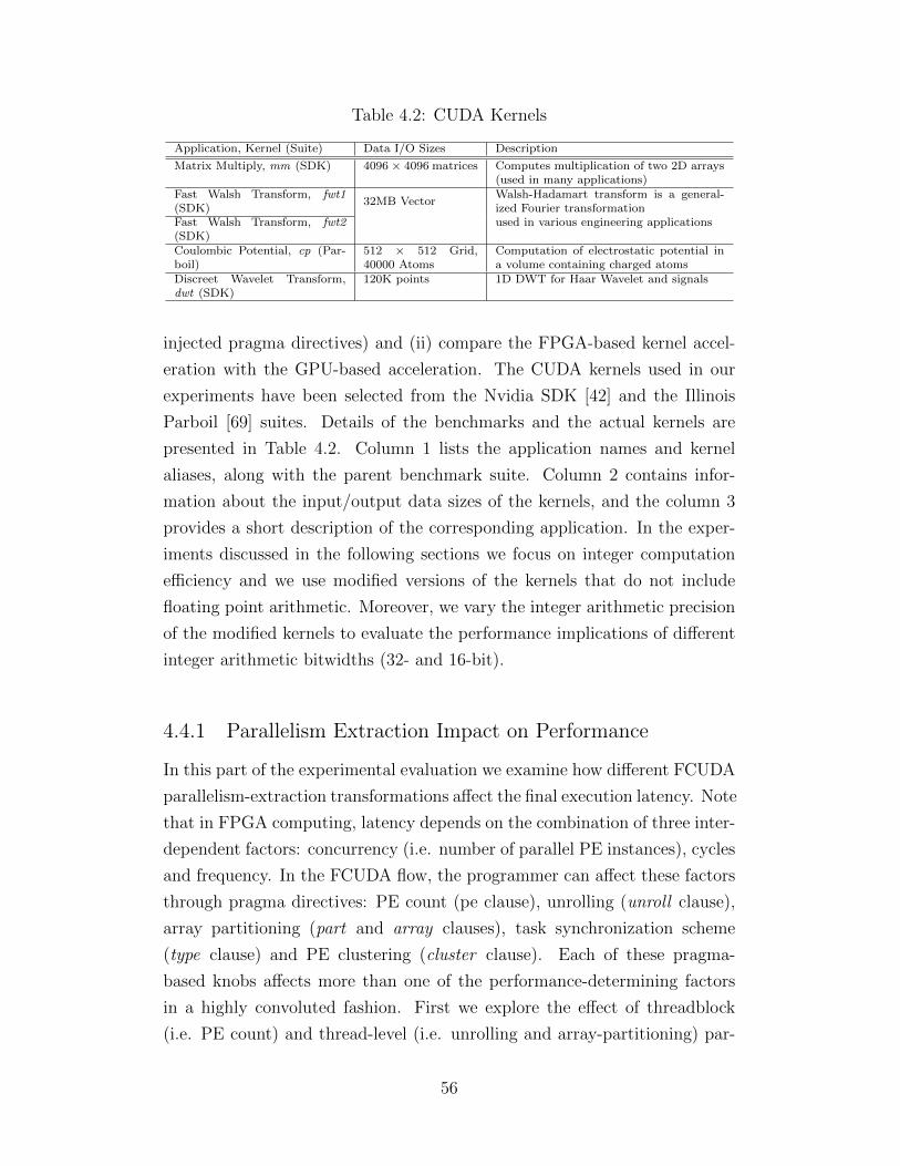
Table 4.2: CUDA Kernels
Application, Kernel (Suite) Data I/O Sizes Description
Matrix Multiply, mm (SDK) 4096 × 4096 matrices Computes multiplication of two 2D arrays(used in many applications)
Fast Walsh Transform, fwt1(SDK)
32MB VectorWalsh-Hadamart transform is a general-ized Fourier transformation
Fast Walsh Transform, fwt2(SDK)
used in various engineering applications
Coulombic Potential, cp (Par-boil)
512 × 512 Grid,40000 Atoms
Computation of electrostatic potential ina volume containing charged atoms
Discreet Wavelet Transform,dwt (SDK)
120K points 1D DWT for Haar Wavelet and signals
injected pragma directives) and (ii) compare the FPGA-based kernel accel-
eration with the GPU-based acceleration. The CUDA kernels used in our
experiments have been selected from the Nvidia SDK [42] and the Illinois
Parboil [69] suites. Details of the benchmarks and the actual kernels are
presented in Table 4.2. Column 1 lists the application names and kernel
aliases, along with the parent benchmark suite. Column 2 contains infor-
mation about the input/output data sizes of the kernels, and the column 3
provides a short description of the corresponding application. In the exper-
iments discussed in the following sections we focus on integer computation
efficiency and we use modified versions of the kernels that do not include
floating point arithmetic. Moreover, we vary the integer arithmetic precision
of the modified kernels to evaluate the performance implications of different
integer arithmetic bitwidths (32- and 16-bit).
4.4.1 Parallelism Extraction Impact on Performance
In this part of the experimental evaluation we examine how different FCUDA
parallelism-extraction transformations affect the final execution latency. Note
that in FPGA computing, latency depends on the combination of three inter-
dependent factors: concurrency (i.e. number of parallel PE instances), cycles
and frequency. In the FCUDA flow, the programmer can affect these factors
through pragma directives: PE count (pe clause), unrolling (unroll clause),
array partitioning (part and array clauses), task synchronization scheme
(type clause) and PE clustering (cluster clause). Each of these pragma-
based knobs affects more than one of the performance-determining factors
in a highly convoluted fashion. First we explore the effect of threadblock
(i.e. PE count) and thread-level (i.e. unrolling and array-partitioning) par-
56
allelism on kernel execution latency. Then we discuss the impact of task
synchronization schemes in performance. Performance evaluation of all the
FPGA implementations is based on frequency and execution cycles obtained
after placement and routing. For the following experiments we use the Xilinx
Virtex5-VSX240T device and we set the number of PE clusters equal to nine
(clustering the PEs in big FPGA devices helps to achieve netlists with rea-
sonable frequencies, whereas logic and physical synthesis runtimes are also
reduced).
Threadblock and Thread level Parallelism
In order to evaluate the effect of threadblock-level and thread-level paral-
lelism in the performance of the synthesized hardware we compare three
parallelism extraction schemes:
maxP represents the designs that expose parallelism primarily at the thread-
block level, i.e the PE count is maximized given a resource constraint.
Thread-level parallelism may also be extracted if remaining resource is
sufficient.
maxPxU represents the designs that maximize the total concurrency, i.e.
the product of PEs and thread-loop unroll degree (pe unroll). Array
partitioning may also be used if remaining resource is sufficient.
maxPxUxM represents the designs that maximize the concurrency along
with the on-chip memory bandwidth, i.e. the product of PE count,
unroll degree and array partitioning (pe× unroll × part).
Tables 4.3–4.5 list the design parameters selected for all the kernels under
the three different parallelism extraction schemes. As expected, the maxP
scheme entails high PE counts with almost no thread-loop unrolling or array
partitioning. Additionally, the maxPxU scheme instantiates fewer PEs but
entails high PEunroll concurrency with almost no array partitioning. Finally,
maxPxUxM results in less PEs than the two previous schemes, but facilitates
high unroll and partitioning factors achieving maximum pe × unroll × partproducts.
Figure 4.6 depicts the kernel execution latencies for the three schemes
(normalized against the latencies of the maxP scheme). We can observe
57
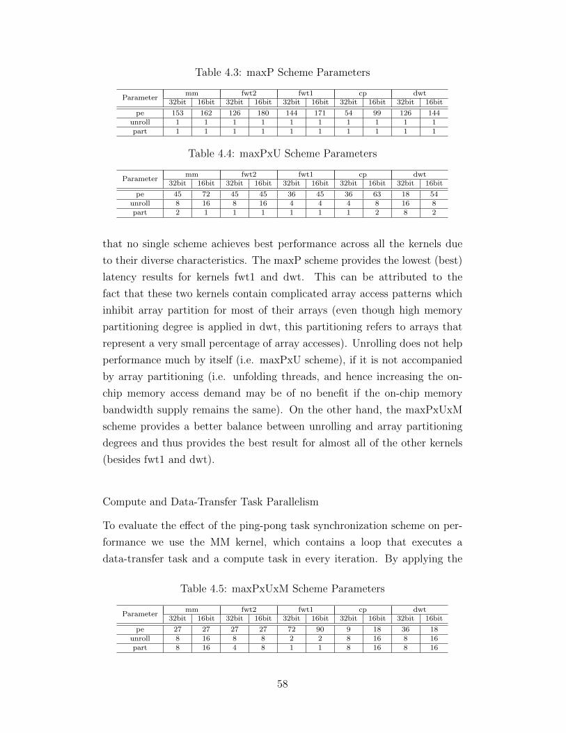
Table 4.3: maxP Scheme Parameters
Parametermm fwt2 fwt1 cp dwt
32bit 16bit 32bit 16bit 32bit 16bit 32bit 16bit 32bit 16bit
pe 153 162 126 180 144 171 54 99 126 144unroll 1 1 1 1 1 1 1 1 1 1part 1 1 1 1 1 1 1 1 1 1
Table 4.4: maxPxU Scheme Parameters
Parametermm fwt2 fwt1 cp dwt
32bit 16bit 32bit 16bit 32bit 16bit 32bit 16bit 32bit 16bit
pe 45 72 45 45 36 45 36 63 18 54unroll 8 16 8 16 4 4 4 8 16 8part 2 1 1 1 1 1 1 2 8 2
that no single scheme achieves best performance across all the kernels due
to their diverse characteristics. The maxP scheme provides the lowest (best)
latency results for kernels fwt1 and dwt. This can be attributed to the
fact that these two kernels contain complicated array access patterns which
inhibit array partition for most of their arrays (even though high memory
partitioning degree is applied in dwt, this partitioning refers to arrays that
represent a very small percentage of array accesses). Unrolling does not help
performance much by itself (i.e. maxPxU scheme), if it is not accompanied
by array partitioning (i.e. unfolding threads, and hence increasing the on-
chip memory access demand may be of no benefit if the on-chip memory
bandwidth supply remains the same). On the other hand, the maxPxUxM
scheme provides a better balance between unrolling and array partitioning
degrees and thus provides the best result for almost all of the other kernels
(besides fwt1 and dwt).
Compute and Data-Transfer Task Parallelism
To evaluate the effect of the ping-pong task synchronization scheme on per-
formance we use the MM kernel, which contains a loop that executes a
data-transfer task and a compute task in every iteration. By applying the
Table 4.5: maxPxUxM Scheme Parameters
Parametermm fwt2 fwt1 cp dwt
32bit 16bit 32bit 16bit 32bit 16bit 32bit 16bit 32bit 16bit
pe 27 27 27 27 72 90 9 18 36 18unroll 8 16 8 8 2 2 8 16 8 16part 8 16 4 8 1 1 8 16 8 16
58
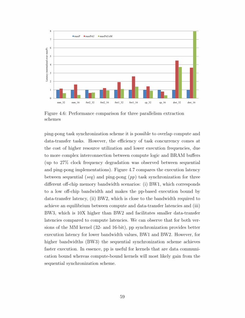
3
4
5
6
7
8
Late
ncy
(nor
mal
ized
ove
r max
P)
maxP maxPxU maxPxUxM
0
1
2
3
4
5
6
7
8
mm_32 mm_16 fwt2_32 fwt2_16 fwt1_32 fwt1_16 cp_32 cp_16 dwt_32 dwt_16
Late
ncy
(nor
mal
ized
ove
r max
P)
maxP maxPxU maxPxUxM
Figure 4.6: Performance comparison for three parallelism extractionschemes
ping-pong task synchronization scheme it is possible to overlap compute and
data-transfer tasks. However, the efficiency of task concurrency comes at
the cost of higher resource utilization and lower execution frequencies, due
to more complex interconnection between compute logic and BRAM buffers
(up to 27% clock frequency degradation was observed between sequential
and ping-pong implementations). Figure 4.7 compares the execution latency
between sequential (seq) and ping-pong (pp) task synchronization for three
different off-chip memory bandwidth scenarios: (i) BW1, which corresponds
to a low off-chip bandwidth and makes the pp-based execution bound by
data-transfer latency, (ii) BW2, which is close to the bandwidth required to
achieve an equilibrium between compute and data-transfer latencies and (iii)
BW3, which is 10X higher than BW2 and facilitates smaller data-transfer
latencies compared to compute latencies. We can observe that for both ver-
sions of the MM kernel (32- and 16-bit), pp synchronization provides better
execution latency for lower bandwidth values, BW1 and BW2. However, for
higher bandwidths (BW3) the sequential synchronization scheme achieves
faster execution. In essence, pp is useful for kernels that are data communi-
cation bound whereas compute-bound kernels will most likely gain from the
sequential synchronization scheme.
59
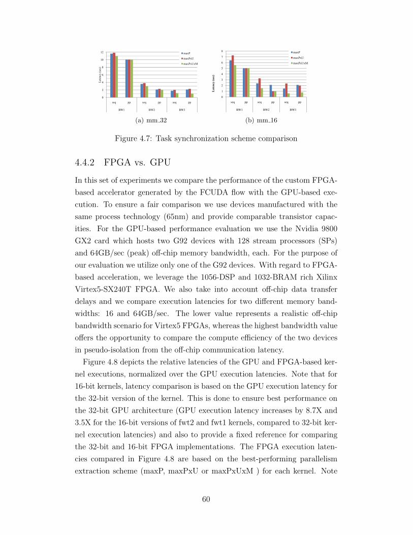
2
4
6
8
10
12
Late
ncy
(sec
)
maxP
maxPxU
maxPxUxM
0
2
4
6
8
10
12
seq pp seq pp seq pp
BW1 BW2 BW3
Late
ncy
(sec
)
maxP
maxPxU
maxPxUxM
(a) mm 32
2
3
4
5
6
7
8
aten
cy (s
ec)
maxP
maxPxU
maxPxUxM
0
1
2
3
4
5
6
7
8
seq pp seq pp seq pp
BW1 BW2 BW3
Lat
ency
(sec
)
maxP
maxPxU
maxPxUxM
(b) mm 16
Figure 4.7: Task synchronization scheme comparison
4.4.2 FPGA vs. GPU
In this set of experiments we compare the performance of the custom FPGA-
based accelerator generated by the FCUDA flow with the GPU-based exe-
cution. To ensure a fair comparison we use devices manufactured with the
same process technology (65nm) and provide comparable transistor capac-
ities. For the GPU-based performance evaluation we use the Nvidia 9800
GX2 card which hosts two G92 devices with 128 stream processors (SPs)
and 64GB/sec (peak) off-chip memory bandwidth, each. For the purpose of
our evaluation we utilize only one of the G92 devices. With regard to FPGA-
based acceleration, we leverage the 1056-DSP and 1032-BRAM rich Xilinx
Virtex5-SX240T FPGA. We also take into account off-chip data transfer
delays and we compare execution latencies for two different memory band-
widths: 16 and 64GB/sec. The lower value represents a realistic off-chip
bandwidth scenario for Virtex5 FPGAs, whereas the highest bandwidth value
offers the opportunity to compare the compute efficiency of the two devices
in pseudo-isolation from the off-chip communication latency.
Figure 4.8 depicts the relative latencies of the GPU and FPGA-based ker-
nel executions, normalized over the GPU execution latencies. Note that for
16-bit kernels, latency comparison is based on the GPU execution latency for
the 32-bit version of the kernel. This is done to ensure best performance on
the 32-bit GPU architecture (GPU execution latency increases by 8.7X and
3.5X for the 16-bit versions of fwt2 and fwt1 kernels, compared to 32-bit ker-
nel execution latencies) and also to provide a fixed reference for comparing
the 32-bit and 16-bit FPGA implementations. The FPGA execution laten-
cies compared in Figure 4.8 are based on the best-performing parallelism
extraction scheme (maxP, maxPxU or maxPxUxM ) for each kernel. Note
60
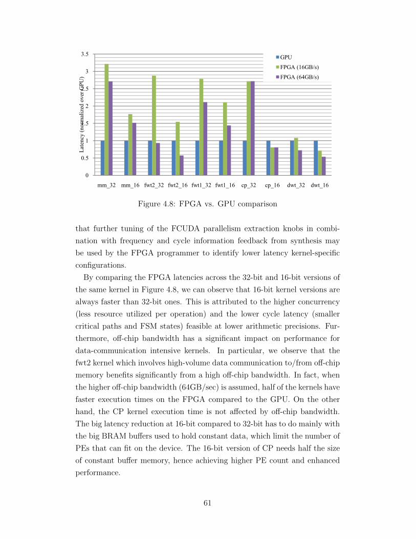
1
1.5
2
2.5
3
3.5
ncy
(nor
mal
ized
ove
r GPU
)
GPU
FPGA (16GB/s)
FPGA (64GB/s)
0
0.5
1
1.5
2
2.5
3
3.5
mm_32 mm_16 fwt2_32 fwt2_16 fwt1_32 fwt1_16 cp_32 cp_16 dwt_32 dwt_16
Late
ncy
(nor
mal
ized
ove
r GPU
)
GPU
FPGA (16GB/s)
FPGA (64GB/s)
Figure 4.8: FPGA vs. GPU comparison
that further tuning of the FCUDA parallelism extraction knobs in combi-
nation with frequency and cycle information feedback from synthesis may
be used by the FPGA programmer to identify lower latency kernel-specific
configurations.
By comparing the FPGA latencies across the 32-bit and 16-bit versions of
the same kernel in Figure 4.8, we can observe that 16-bit kernel versions are
always faster than 32-bit ones. This is attributed to the higher concurrency
(less resource utilized per operation) and the lower cycle latency (smaller
critical paths and FSM states) feasible at lower arithmetic precisions. Fur-
thermore, off-chip bandwidth has a significant impact on performance for
data-communication intensive kernels. In particular, we observe that the
fwt2 kernel which involves high-volume data communication to/from off-chip
memory benefits significantly from a high off-chip bandwidth. In fact, when
the higher off-chip bandwidth (64GB/sec) is assumed, half of the kernels have
faster execution times on the FPGA compared to the GPU. On the other
hand, the CP kernel execution time is not affected by off-chip bandwidth.
The big latency reduction at 16-bit compared to 32-bit has to do mainly with
the big BRAM buffers used to hold constant data, which limit the number of
PEs that can fit on the device. The 16-bit version of CP needs half the size
of constant buffer memory, hence achieving higher PE count and enhanced
performance.
61
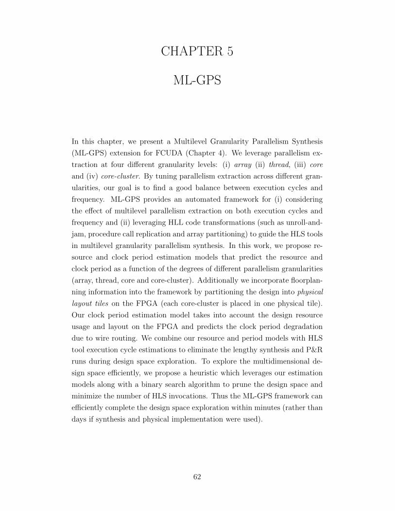
CHAPTER 5
ML-GPS
In this chapter, we present a Multilevel Granularity Parallelism Synthesis
(ML-GPS) extension for FCUDA (Chapter 4). We leverage parallelism ex-
traction at four different granularity levels: (i) array (ii) thread, (iii) core
and (iv) core-cluster. By tuning parallelism extraction across different gran-
ularities, our goal is to find a good balance between execution cycles and
frequency. ML-GPS provides an automated framework for (i) considering
the effect of multilevel parallelism extraction on both execution cycles and
frequency and (ii) leveraging HLL code transformations (such as unroll-and-
jam, procedure call replication and array partitioning) to guide the HLS tools
in multilevel granularity parallelism synthesis. In this work, we propose re-
source and clock period estimation models that predict the resource and
clock period as a function of the degrees of different parallelism granularities
(array, thread, core and core-cluster). Additionally we incorporate floorplan-
ning information into the framework by partitioning the design into physical
layout tiles on the FPGA (each core-cluster is placed in one physical tile).
Our clock period estimation model takes into account the design resource
usage and layout on the FPGA and predicts the clock period degradation
due to wire routing. We combine our resource and period models with HLS
tool execution cycle estimations to eliminate the lengthy synthesis and P&R
runs during design space exploration. To explore the multidimensional de-
sign space efficiently, we propose a heuristic which leverages our estimation
models along with a binary search algorithm to prune the design space and
minimize the number of HLS invocations. Thus the ML-GPS framework can
efficiently complete the design space exploration within minutes (rather than
days if synthesis and physical implementation were used).
62
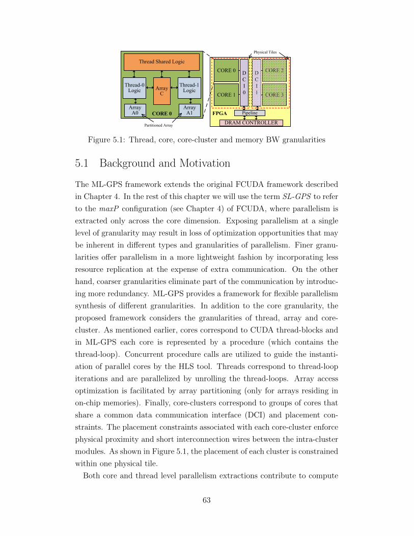
CORE 0
CORE 0
Thread Shared Logic
Thread-0 Logic
Thread-1 LogicArray
C
Array A0
Array A1
CORE 1
DRAM CONTROLLER
DCI1
FPGA
CORE 3
CORE 2DCI0
Pipeline
Physical Tiles
Partitioned Array
Figure 5.1: Thread, core, core-cluster and memory BW granularities
5.1 Background and Motivation
The ML-GPS framework extends the original FCUDA framework described
in Chapter 4. In the rest of this chapter we will use the term SL-GPS to refer
to the maxP configuration (see Chapter 4) of FCUDA, where parallelism is
extracted only across the core dimension. Exposing parallelism at a single
level of granularity may result in loss of optimization opportunities that may
be inherent in different types and granularities of parallelism. Finer granu-
larities offer parallelism in a more lightweight fashion by incorporating less
resource replication at the expense of extra communication. On the other
hand, coarser granularities eliminate part of the communication by introduc-
ing more redundancy. ML-GPS provides a framework for flexible parallelism
synthesis of different granularities. In addition to the core granularity, the
proposed framework considers the granularities of thread, array and core-
cluster. As mentioned earlier, cores correspond to CUDA thread-blocks and
in ML-GPS each core is represented by a procedure (which contains the
thread-loop). Concurrent procedure calls are utilized to guide the instanti-
ation of parallel cores by the HLS tool. Threads correspond to thread-loop
iterations and are parallelized by unrolling the thread-loops. Array access
optimization is facilitated by array partitioning (only for arrays residing in
on-chip memories). Finally, core-clusters correspond to groups of cores that
share a common data communication interface (DCI) and placement con-
straints. The placement constraints associated with each core-cluster enforce
physical proximity and short interconnection wires between the intra-cluster
modules. As shown in Figure 5.1, the placement of each cluster is constrained
within one physical tile.
Both core and thread level parallelism extractions contribute to compute
63
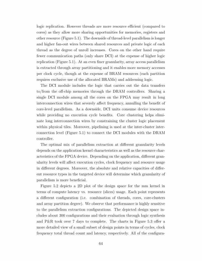
logic replication. However threads are more resource efficient (compared to
cores) as they allow more sharing opportunities for memories, registers and
other resource (Figure 5.1). The downside of thread-level parallelism is longer
and higher fan-out wires between shared resources and private logic of each
thread as the degree of unroll increases. Cores on the other hand require
fewer communication paths (only share DCI) at the expense of higher logic
replication (Figure 5.1). At an even finer granularity, array access parallelism
is extracted through array partitioning and it enables more memory accesses
per clock cycle, though at the expense of BRAM resources (each partition
requires exclusive use of the allocated BRAMs) and addressing logic.
The DCI module includes the logic that carries out the data transfers
to/from the off-chip memories through the DRAM controllers. Sharing a
single DCI module among all the cores on the FPGA may result in long
interconnection wires that severely affect frequency, annulling the benefit of
core-level parallelism. As a downside, DCI units consume device resources
while providing no execution cycle benefits. Core clustering helps elimi-
nate long interconnection wires by constraining the cluster logic placement
within physical tiles. Moreover, pipelining is used at the inter-cluster inter-
connection level (Figure 5.1) to connect the DCI modules with the DRAM
controller.
The optimal mix of parallelism extraction at different granularity levels
depends on the application kernel characteristics as well as the resource char-
acteristics of the FPGA device. Depending on the application, different gran-
ularity levels will affect execution cycles, clock frequency and resource usage
in different degrees. Moreover, the absolute and relative capacities of differ-
ent resource types in the targeted device will determine which granularity of
parallelism is more beneficial.
Figure 5.2 depicts a 2D plot of the design space for the mm kernel in
terms of compute latency vs. resource (slices) usage. Each point represents
a different configuration (i.e. combination of threads, cores, core-clusters
and array partition degree). We observe that performance is highly sensitive
to the parallelism extraction configurations. The depicted design space in-
cludes about 300 configurations and their evaluation through logic synthesis
and P&R took over 7 days to complete. The charts in Figure 5.3 offer a
more detailed view of a small subset of design points in terms of cycles, clock
frequency total thread count and latency, respectively. All of the configura-
64
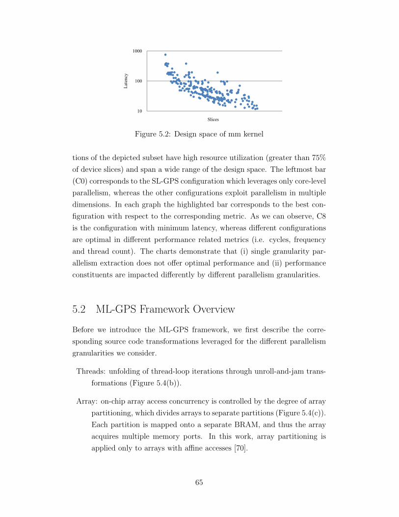
100
1000
Late
ncy
10
100
1000
Late
ncy
Slices
Figure 5.2: Design space of mm kernel
tions of the depicted subset have high resource utilization (greater than 75%
of device slices) and span a wide range of the design space. The leftmost bar
(C0) corresponds to the SL-GPS configuration which leverages only core-level
parallelism, whereas the other configurations exploit parallelism in multiple
dimensions. In each graph the highlighted bar corresponds to the best con-
figuration with respect to the corresponding metric. As we can observe, C8
is the configuration with minimum latency, whereas different configurations
are optimal in different performance related metrics (i.e. cycles, frequency
and thread count). The charts demonstrate that (i) single granularity par-
allelism extraction does not offer optimal performance and (ii) performance
constituents are impacted differently by different parallelism granularities.
5.2 ML-GPS Framework Overview
Before we introduce the ML-GPS framework, we first describe the corre-
sponding source code transformations leveraged for the different parallelism
granularities we consider.
Threads: unfolding of thread-loop iterations through unroll-and-jam trans-
formations (Figure 5.4(b)).
Array: on-chip array access concurrency is controlled by the degree of array
partitioning, which divides arrays to separate partitions (Figure 5.4(c)).
Each partition is mapped onto a separate BRAM, and thus the array
acquires multiple memory ports. In this work, array partitioning is
applied only to arrays with affine accesses [70].
65
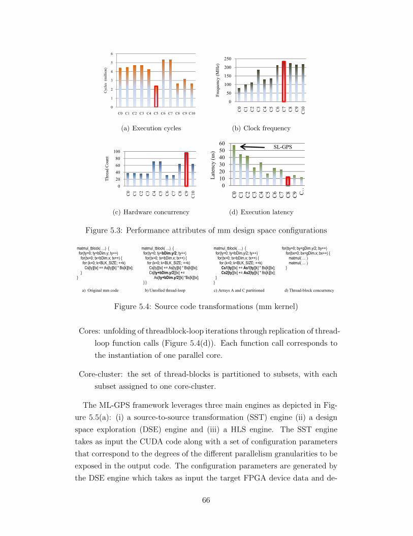
2
3
4
5
6
Cyc
les
(mill
ion)
0
1
2
3
4
5
6
C0 C1 C2 C3 C4 C5 C6 C7 C8 C9 C10
Cyc
les
(mill
ion)
(a) Execution cycles
50
100
150
200
250
Freq
uenc
y (M
Hz)
0
50
100
150
200
250
C0
C1
C2
C3
C4
C5
C6
C7
C8
C9
C10
Freq
uenc
y (M
Hz)
(b) Clock frequency
020406080
100
Thre
ad C
ount
020406080
100
C0
C1
C2
C3
C4
C5
C6
C7
C8
C9
C10
Thre
ad C
ount
(c) Hardware concurrency
102030405060
Late
ncy
(us)
SL-GPS
0102030405060
C0
C1
C2
C3
C4
C5
C6
C7
C8
C9 C
…
Late
ncy
(us)
SL-GPS
(d) Execution latency
Figure 5.3: Performance attributes of mm design space configurations
Threads: unfolding of thread-loop iterations through unroll-and-jam transformations (Fig 4b).
Array: on-chip array access concurrency is controlled by the degree of array partitioning, which divides arrays to separate partitions (Fig. 4c). Each partition is mapped onto a separate BRAM and thus, the array acquires multiple memory ports. In this work, array partitioning is applied only to arrays with affine accesses [19].
Cores: unfolding of threadblock-loop iterations through replication of thread-loop function calls (Fig. 4d). Each function call corresponds to the instantiation of one parallel core.
Core-cluster: the set of thread-blocks is partitioned to subsets, with each subset assigned to one core-cluster.
The ML-GPS framework leverages three main engines as depicted in Fig. 5a: i) a source-to-source transformation (SST) engine ii) a design space exploration (DSE) engine and iii) a HLS engine. The SST engine takes as input the CUDA code along with a set of configuration parameters that correspond to the degrees of the different parallelism granularities to be exposed in the output code. The configuration parameters are generated by the DSE engine which takes as input the target FPGA device data and determines the configurations that should be evaluated during the design space exploration. Finally, the HLS engine synthesizes the generated output code of the SST engine to RTL. In the ML-GPS framework we use a commercial HLS tool [2], which generates highly-optimized RTL code.
The ML-GPS flow involves three automated main steps (Fig. 5b). Initially a kernel profiling step is performed in order to build the resource estimation model for each kernel. Profiling entails feeding the SST engine with a small set of multilevel granularity configurations which are subsequently synthesized by the HLS tool to generate the corresponding resource utilization estimations. A kernel-specific resource model is then built using regression analysis on the HLS resource estimations. The number of the profiled
configuration points determines the accuracy of the resource estimation model generated. More configurations result in more accurate resource models, though, at the expense of extra profiling time. In the ML-GPS framework the user can determine the effort spent on profiling.
After profiling, the design space is determined in the second main step. First the total number of core-cluster configurations is determined by considering both the resource estimation model generated in the 1st step (i.e. take into account the kernel characteristics) and the selected FPGA device (i.e. take into account the resource availability and distribution on the device). Subsequently the thread, array partitioning and core dimensions of the design space are determined for each core-cluster configuration with the help of the resource estimation model.
Finally in the third main step, design space exploration is performed using the resource and the clock period estimation models along with cycle estimates from the HLS tool to evaluate the performance of the different design points. A binary search heuristic is used to trim down the number of HLS invocations and prune the design space. The DSE engine’s goal is to identify the optimal coordinates in the multi-dimensional parallelism granularity space in order to maximize the performance of the CUDA kernel on the selected FPGA device (i.e. given a fixed resource budget).
IV. DESIGN SPACE EXPLORATION As mentioned previously, exploration of the multilevel
granularity space is based on estimations of resource, clock period and cycles. We estimate resource and clock period degradation due to routing through regression analysis based equations, whereas we leverage cycle estimations from HLS. The formulas used for resource and clock period estimations are presented in the following section. To optimize the space exploration runtime we employ an efficient search optimization that helps minimize the number of HLS tool invocations during the search process. This is discussed in Section IV.B.
A. Resource and Clock Period Estimation Models The resource model is built during the profiling step of
the flow. A small number of points in the design space are used to generate different configurations of the input kernel exposing different granularities of parallelism. The HLS tool is fed with the profiled kernel configurations and it returns resource estimation results. We classify the resource estimations based on the degrees of parallelism exposed at the core (CR), thread (TH), and array-partitioning (AP) dimensions. Using linear regression we then evaluate the R0, R1, R2 R3 and R4 coefficients of (1):
matmul_tblock( …) { for(ty=0; ty<bDim.y; ty++) for(tx=0; tx<bDim.x; tx++) { for (k=0; k<BLK_SIZE; ++k) Cs[ty][tx] += As[ty][k] * Bs[k][tx]; } }
matmul_tblock( …) { for(ty=0; ty<bDim.y/2; ty++) for(tx=0; tx<bDim.x; tx++) { for (k=0; k<BLK_SIZE; ++k) Cs[ty][tx] += As[ty][k] * Bs[k][tx]; Cs[ty+bDim.y/2][tx] += As[ty+bDim.y/2][k] *Bs[k][tx]; } }
matmul_tblock( …) { for(ty=0; ty<bDim.y/2; ty++) for(tx=0; tx<bDim.x; tx++) { for (k=0; k<BLK_SIZE; ++k) Cs1[ty][tx] += As1[ty][k] * Bs[k][tx]; Cs2[ty][tx] += As2[ty][k] * Bs[k][tx]; } }
for(by=0; by<gDim.y/2; by++) for(bx=0; bx<gDim.x; bx++) { matmul( … ) matmul( … ) }
a) Original mm code b) Unrolled thread-loop c) Arrays A and C partitioned d) Thread-block concurrency
Figure 4. Source code transformations (mm kernel)
a) ML-GPS components b) ML-GPS flow
Figure 5. ML-GPS Overview
Figure 5.4: Source code transformations (mm kernel)
Cores: unfolding of threadblock-loop iterations through replication of thread-
loop function calls (Figure 5.4(d)). Each function call corresponds to
the instantiation of one parallel core.
Core-cluster: the set of thread-blocks is partitioned to subsets, with each
subset assigned to one core-cluster.
The ML-GPS framework leverages three main engines as depicted in Fig-
ure 5.5(a): (i) a source-to-source transformation (SST) engine (ii) a design
space exploration (DSE) engine and (iii) a HLS engine. The SST engine
takes as input the CUDA code along with a set of configuration parameters
that correspond to the degrees of the different parallelism granularities to be
exposed in the output code. The configuration parameters are generated by
the DSE engine which takes as input the target FPGA device data and de-
66
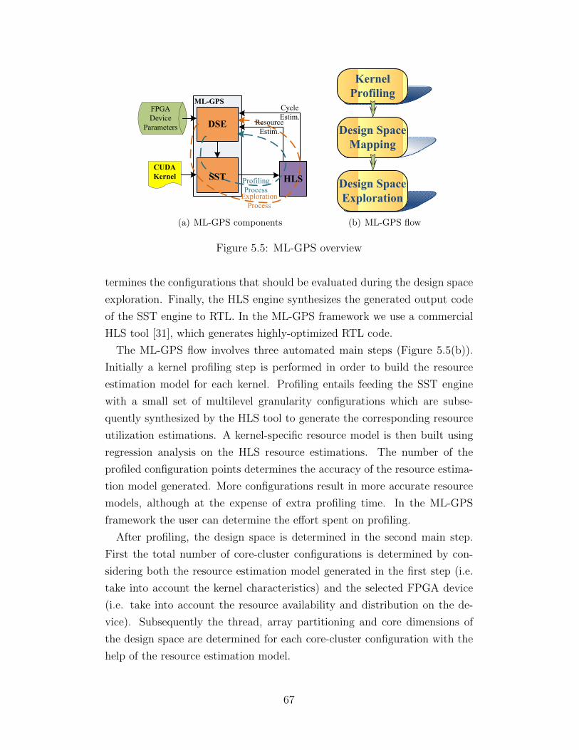
ML-GPS
DSE
CUDA Kernel
FPGA Device
Parameters
Cycle Estim.
Profiling Process
Exploration Process
HLS
Resource Estim.
SST
(a) ML-GPS components
Kernel Profiling
Design Space Mapping
Design Space Exploration
(b) ML-GPS flow
Figure 5.5: ML-GPS overview
termines the configurations that should be evaluated during the design space
exploration. Finally, the HLS engine synthesizes the generated output code
of the SST engine to RTL. In the ML-GPS framework we use a commercial
HLS tool [31], which generates highly-optimized RTL code.
The ML-GPS flow involves three automated main steps (Figure 5.5(b)).
Initially a kernel profiling step is performed in order to build the resource
estimation model for each kernel. Profiling entails feeding the SST engine
with a small set of multilevel granularity configurations which are subse-
quently synthesized by the HLS tool to generate the corresponding resource
utilization estimations. A kernel-specific resource model is then built using
regression analysis on the HLS resource estimations. The number of the
profiled configuration points determines the accuracy of the resource estima-
tion model generated. More configurations result in more accurate resource
models, although at the expense of extra profiling time. In the ML-GPS
framework the user can determine the effort spent on profiling.
After profiling, the design space is determined in the second main step.
First the total number of core-cluster configurations is determined by con-
sidering both the resource estimation model generated in the first step (i.e.
take into account the kernel characteristics) and the selected FPGA device
(i.e. take into account the resource availability and distribution on the de-
vice). Subsequently the thread, array partitioning and core dimensions of
the design space are determined for each core-cluster configuration with the
help of the resource estimation model.
67
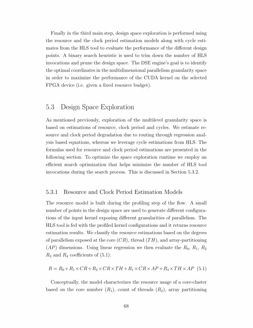
Finally in the third main step, design space exploration is performed using
the resource and the clock period estimation models along with cycle esti-
mates from the HLS tool to evaluate the performance of the different design
points. A binary search heuristic is used to trim down the number of HLS
invocations and prune the design space. The DSE engine’s goal is to identify
the optimal coordinates in the multidimensional parallelism granularity space
in order to maximize the performance of the CUDA kernel on the selected
FPGA device (i.e. given a fixed resource budget).
5.3 Design Space Exploration
As mentioned previously, exploration of the multilevel granularity space is
based on estimations of resource, clock period and cycles. We estimate re-
source and clock period degradation due to routing through regression anal-
ysis based equations, whereas we leverage cycle estimations from HLS. The
formulas used for resource and clock period estimations are presented in the
following section. To optimize the space exploration runtime we employ an
efficient search optimization that helps minimize the number of HLS tool
invocations during the search process. This is discussed in Section 5.3.2.
5.3.1 Resource and Clock Period Estimation Models
The resource model is built during the profiling step of the flow. A small
number of points in the design space are used to generate different configura-
tions of the input kernel exposing different granularities of parallelism. The
HLS tool is fed with the profiled kernel configurations and it returns resource
estimation results. We classify the resource estimations based on the degrees
of parallelism exposed at the core (CR), thread (TH), and array-partitioning
(AP ) dimensions. Using linear regression we then evaluate the R0, R1, R2
R3 and R4 coefficients of (5.1):
R = R0 +R1×CR+R2×CR×TH+R1×CR×AP +R4×TH×AP (5.1)
Conceptually, the model characterizes the resource usage of a core-cluster
based on the core number (R1), count of threads (R2), array partitioning
68
(R3), and the interaction between unrolling and array partitioning (R4). For
each type of resource (LUT, Flip-Flop, BRAM and DSP) we construct a sep-
arate equation which represents the core-cluster resource usage as a function
of the different parallelism granularities. These equations are kernel-specific
and are used during the design space exploration phase for resource budgeting
as well as for estimating the clock period. The total resource count, RFPGA, is
equal to the product of the core-cluster resource estimation, R, and the num-
ber of physical tiles, CL, (i.e. number of core-clusters): RFPGA = R× CL.
The clock period model aims to capture the clock period degradation re-
sulting from wire routing within the core-cluster. The HLS-generated RTL is
pipelined for a nominal clock period defined by the user. However the actual
clock period of the placed netlist is often degraded (i.e. lengthened) due to
interconnection wire delays introduced during P&R. Through this model we
incorporate the effect of different parallelism granularities as well as layout
information on interconnection wires (i.e. wires within the core cluster; inter-
cluster wires are pipelined appropriately, as mentioned earlier) and thus the
clock period. The period estimation model is described by (5.2) which is
pre-fitted offline using synthesis data (synthesized CUDA kernels were used
for the period estimation model construction):
Period = P0 + P1 ×Diag + P2 × Util + P3 × AP + P4 × TH (5.2)
Diag is calculated using (5.3) and it corresponds to the diagonal length (in
slices) of a virtual tile with the following properties: (i) the total core-cluster
slices can fit in the virtual tile, (ii) the dimensions of the virtual tile do not
exceed the dimensions of the allocated physical tile and (iii) the diagonal
length of the virtual tile is minimal given the two previous constraints. Util
in (5.2) represents the slice utilization rate of the physical tile by the core-
cluster logic.
Diag2 =
2×Rslice , ifRslice ≤ minDim2
minDim2 +(
Rslice
minDim
)2, ifRslice > minDim2
(5.3)
where minDim corresponds to the minimum dimension of the physical tile
(in slices) and Rslice is the slice count of the core-cluster logic. Parameters
Rslice (hence Diag) and Util in (5.2) are calculated by leveraging the re-
69
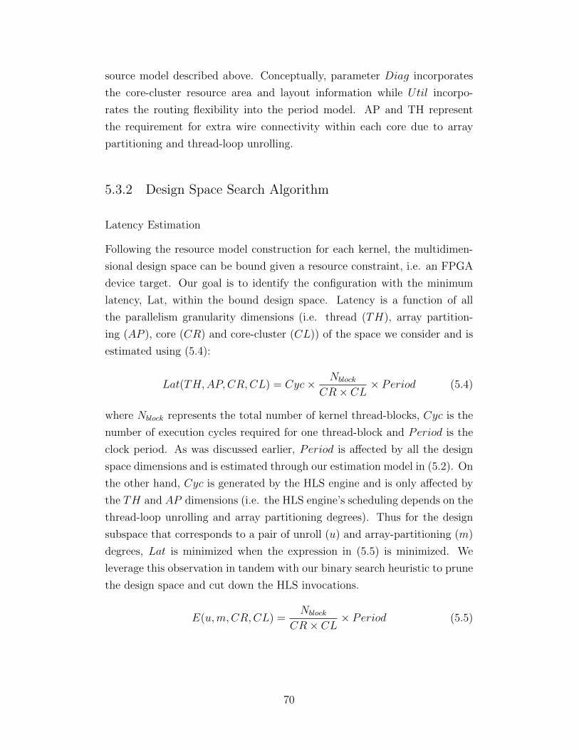
source model described above. Conceptually, parameter Diag incorporates
the core-cluster resource area and layout information while Util incorpo-
rates the routing flexibility into the period model. AP and TH represent
the requirement for extra wire connectivity within each core due to array
partitioning and thread-loop unrolling.
5.3.2 Design Space Search Algorithm
Latency Estimation
Following the resource model construction for each kernel, the multidimen-
sional design space can be bound given a resource constraint, i.e. an FPGA
device target. Our goal is to identify the configuration with the minimum
latency, Lat, within the bound design space. Latency is a function of all
the parallelism granularity dimensions (i.e. thread (TH), array partition-
ing (AP ), core (CR) and core-cluster (CL)) of the space we consider and is
estimated using (5.4):
Lat(TH,AP,CR,CL) = Cyc× Nblock
CR× CL× Period (5.4)
where Nblock represents the total number of kernel thread-blocks, Cyc is the
number of execution cycles required for one thread-block and Period is the
clock period. As was discussed earlier, Period is affected by all the design
space dimensions and is estimated through our estimation model in (5.2). On
the other hand, Cyc is generated by the HLS engine and is only affected by
the TH and AP dimensions (i.e. the HLS engine’s scheduling depends on the
thread-loop unrolling and array partitioning degrees). Thus for the design
subspace that corresponds to a pair of unroll (u) and array-partitioning (m)
degrees, Lat is minimized when the expression in (5.5) is minimized. We
leverage this observation in tandem with our binary search heuristic to prune
the design space and cut down the HLS invocations.
E(u,m,CR,CL) =Nblock
CR× CL× Period (5.5)
70
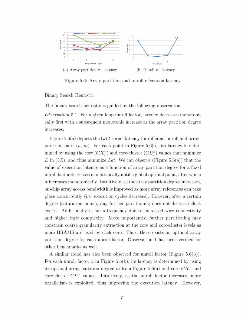
11.5
22.5
33.5
4
Late
ncy
(ms)
unroll-4 unroll-8 unroll-16
00.5
11.5
22.5
33.5
4
1 2 4 8La
tenc
y (m
s)
Array Partition Degree
unroll-4 unroll-8 unroll-16
(a) Array partition vs. latency
1.4
1.6
1.8
2
Late
ncy
(ms)
1
12 4
4
1
1.2
1.4
1.6
1.8
2
1 2 4 8 16
Late
ncy
(ms)
Unroll Factor
1
12 4
4
(b) Unroll vs. latency
Figure 5.6: Array partition and unroll effects on latency
Binary Search Heuristic
The binary search heuristic is guided by the following observation:
Observation 5.1. For a given loop unroll factor, latency decreases monotoni-
cally first with a subsequent monotonic increase as the array partition degree
increases.
Figure 5.6(a) depicts the fwt2 kernel latency for different unroll and array-
partition pairs (u, m). For each point in Figure 5.6(a), its latency is deter-
mined by using the core (CRmu ) and core-cluster (CLm
u ) values that minimize
E in (5.5), and thus minimize Lat. We can observe (Figure 5.6(a)) that the
value of execution latency as a function of array partition degree for a fixed
unroll factor decreases monotonically until a global optimal point, after which
it increases monotonically. Intuitively, as the array partition degree increases,
on-chip array access bandwidth is improved as more array references can take
place concurrently (i.e. execution cycles decrease). However, after a certain
degree (saturation point), any further partitioning does not decrease clock
cycles. Additionally it hurts frequency due to increased wire connectivity
and higher logic complexity. More importantly, further partitioning may
constrain coarse granularity extraction at the core and core-cluster levels as
more BRAMS are used by each core. Thus, there exists an optimal array
partition degree for each unroll factor. Observation 1 has been verified for
other benchmarks as well.
A similar trend has also been observed for unroll factor (Figure 5.6(b)).
For each unroll factor u in Figure 5.6(b), its latency is determined by using
its optimal array partition degree m from Figure 5.6(a) and core CRmu and
core-cluster CLmu values. Intuitively, as the unroll factor increases, more
parallelism is exploited, thus improving the execution latency. However,
71
unrolling beyond a certain degree may not be beneficial due to array access
bottleneck and frequency degradation (from increased connectivity and fan-
out issues). In summary, there is an optimal unrolling degree.
Based on the above observation and the intuition behind it, in Algo-
rithm 5.1 we propose a binary search algorithm to find the optimal point
(unroll factor u and array partition degree m). As shown in Algorithm 5.1,
we search unroll factor first followed by array partition degree. Array space[]
stores the feasible values for each dimension dim, in sorted order (line 9).
The size and value of space[] are obtained from the resource model. Then,
we perform binary search for dimension dim. In each round of the binary
search (line 11-22), we compare the performance of two middle neighboring
points (mid, mid+1). Function Select records the value selected for the di-
mension dim. The comparison result guides the search towards one direction
(the direction with smaller latency) while the other direction is pruned away.
In the end of the search across each dimension, the best result of the current
dimension (in terms of execution latency) is returned. For each point visited
during the search (i.e. (u, m) pair), the corresponding execution latency is
computed based on (4) (line 6). The function UpdateLatency compares the
current solution with the global best solution and updates it if the current
solution turns out to be better.
Let us consider fwt2, shown in Figure 5.6(b), as an example. We start
searching the unroll degree dimension and compare two neighboring points
in the middle (2 and 4). For each unroll factor (2 and 4), its minimal latency
is returned by recursively searching next dimension in a binary search fashion.
The best solution so far is stored and the latency comparison of unroll factors
(2 and 4) will indicate the subsequent search direction. The complexity of
our binary search is log |U | × log |M |, where U and M represent the design
dimensions of thread and array partition.
5.4 Evaluation
The goals of our experimental study are threefold: (i) to evaluate the ef-
fectiveness of the estimation models and the search algorithm employed in
ML-GPS, (ii) to measure the performance advantage offered by consider-
ing multiple parallelism granularities in ML-GPS versus SL-GPS and (iii) to
72
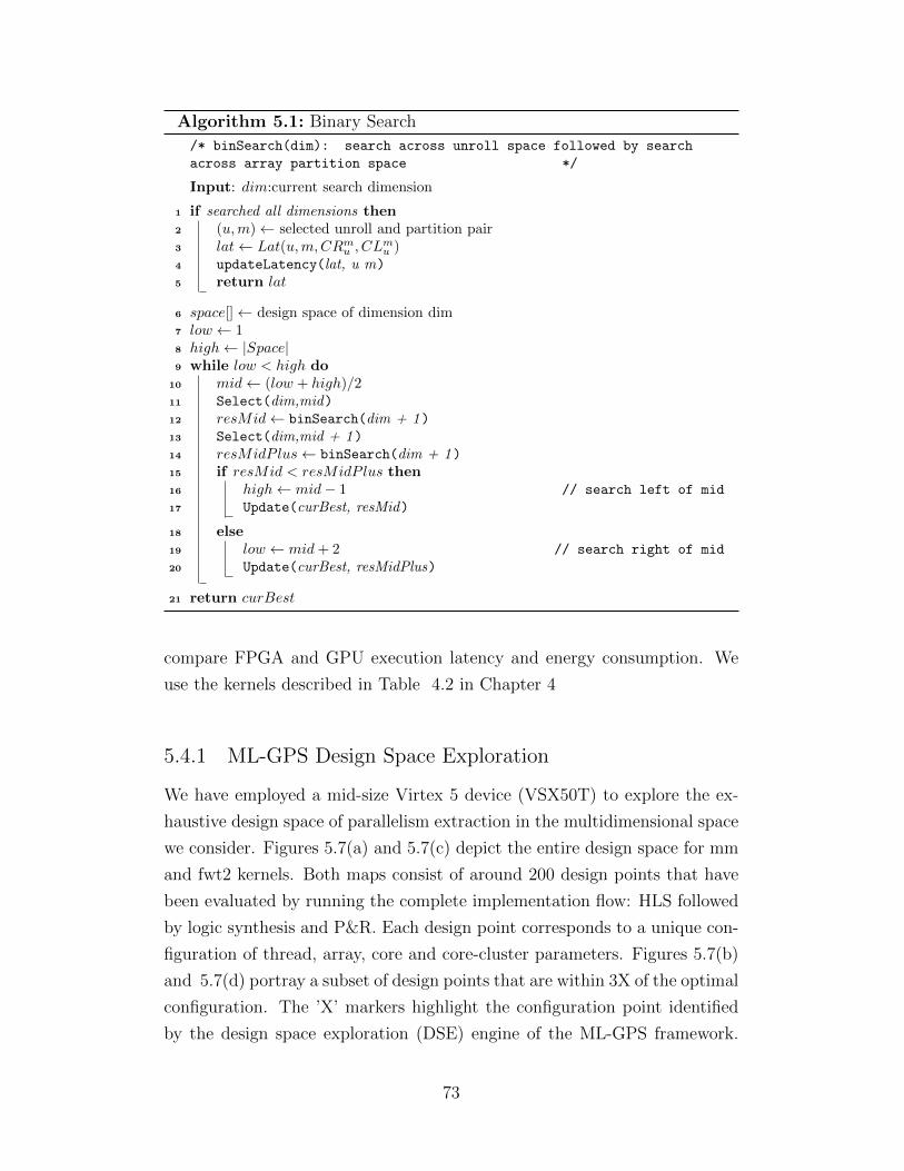
Algorithm 5.1: Binary Search
/* binSearch(dim): search across unroll space followed by search
across array partition space */
Input: dim:current search dimension
1 if searched all dimensions then2 (u,m)← selected unroll and partition pair3 lat← Lat(u,m,CRm
u , CLmu )
4 updateLatency(lat, u m)
5 return lat
6 space[]← design space of dimension dim7 low ← 18 high← |Space|9 while low < high do
10 mid← (low + high)/211 Select(dim,mid)12 resMid← binSearch(dim + 1)13 Select(dim,mid + 1)14 resMidP lus← binSearch(dim + 1)15 if resMid < resMidP lus then16 high← mid− 1 // search left of mid
17 Update(curBest, resMid)
18 else19 low ← mid + 2 // search right of mid
20 Update(curBest, resMidPlus)
21 return curBest
compare FPGA and GPU execution latency and energy consumption. We
use the kernels described in Table 4.2 in Chapter 4
5.4.1 ML-GPS Design Space Exploration
We have employed a mid-size Virtex 5 device (VSX50T) to explore the ex-
haustive design space of parallelism extraction in the multidimensional space
we consider. Figures 5.7(a) and 5.7(c) depict the entire design space for mm
and fwt2 kernels. Both maps consist of around 200 design points that have
been evaluated by running the complete implementation flow: HLS followed
by logic synthesis and P&R. Each design point corresponds to a unique con-
figuration of thread, array, core and core-cluster parameters. Figures 5.7(b)
and 5.7(d) portray a subset of design points that are within 3X of the optimal
configuration. The ’X’ markers highlight the configuration point identified
by the design space exploration (DSE) engine of the ML-GPS framework.
73
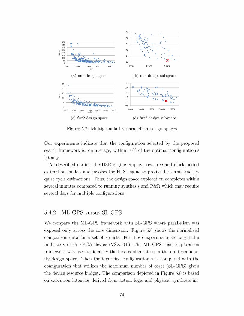
50100150200250300350400
Late
ncy
050
100150200250300350400
2000 7000 12000 17000 22000
Late
ncy
LUTs
(a) mm design space
20
25
30
35
10
15
20
25
30
35
5000 15000 25000
(b) mm design subspace
5
10
15
20
25
Late
ncy
0
5
10
15
20
25
2000 7000 12000 17000 22000 27000 32000
Late
ncy
LUTs
(c) fwt2 design space
1 1
1.6
2.1
2.6
3.1
0.6
1.1
1.6
2.1
2.6
3.1
9000 14000 19000 24000 29000
(d) fwt2 design subspace
Figure 5.7: Multigranularity parallelism design spaces
Our experiments indicate that the configuration selected by the proposed
search framework is, on average, within 10% of the optimal configuration’s
latency.
As described earlier, the DSE engine employs resource and clock period
estimation models and invokes the HLS engine to profile the kernel and ac-
quire cycle estimations. Thus, the design space exploration completes within
several minutes compared to running synthesis and P&R which may require
several days for multiple configurations.
5.4.2 ML-GPS versus SL-GPS
We compare the ML-GPS framework with SL-GPS where parallelism was
exposed only across the core dimension. Figure 5.8 shows the normalized
comparison data for a set of kernels. For these experiments we targeted a
mid-size virtex5 FPGA device (VSX50T). The ML-GPS space exploration
framework was used to identify the best configuration in the multigranular-
ity design space. Then the identified configuration was compared with the
configuration that utilizes the maximum number of cores (SL-GPS) given
the device resource budget. The comparison depicted in Figure 5.8 is based
on execution latencies derived from actual logic and physical synthesis im-
74
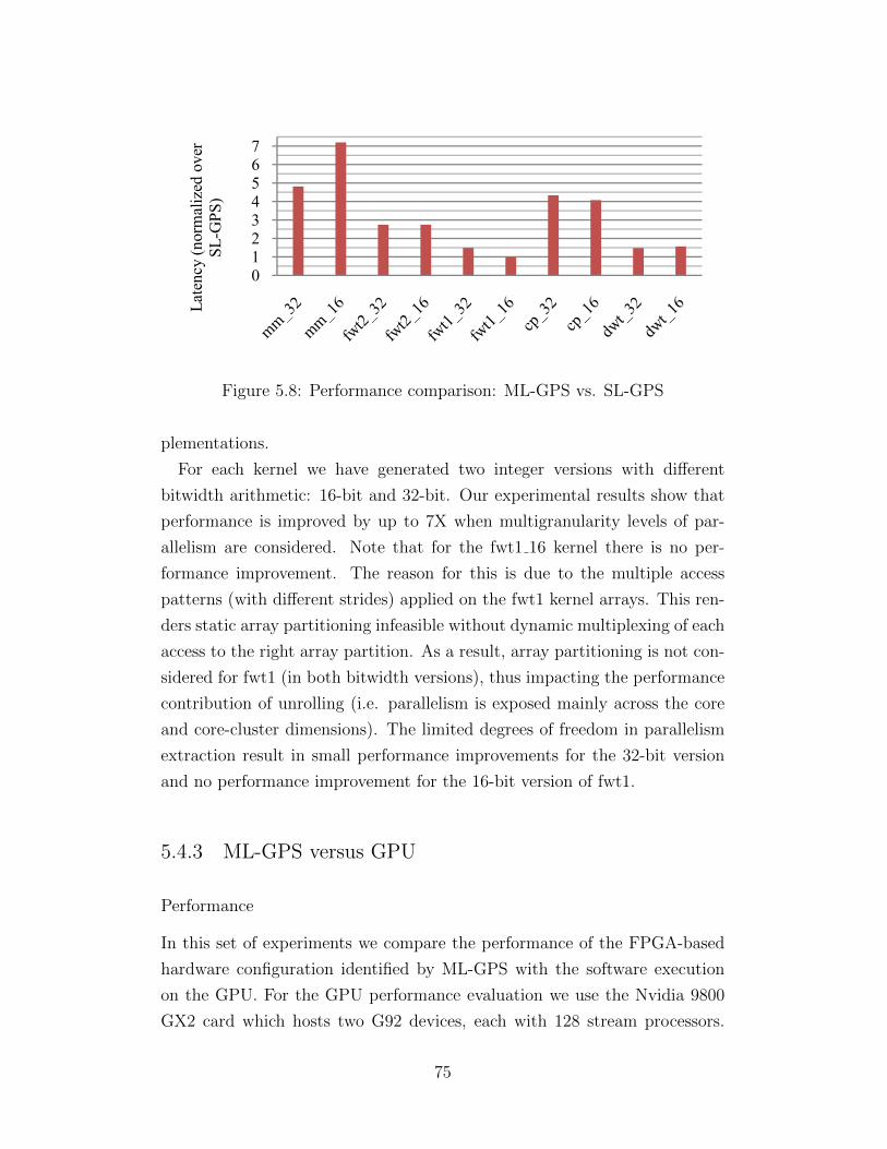
01234567
ency
(nor
mal
ized
ove
r SL
-GPS
)
01234567
Late
ncy
(nor
mal
ized
ove
r SL
-GPS
)
Figure 5.8: Performance comparison: ML-GPS vs. SL-GPS
plementations.
For each kernel we have generated two integer versions with different
bitwidth arithmetic: 16-bit and 32-bit. Our experimental results show that
performance is improved by up to 7X when multigranularity levels of par-
allelism are considered. Note that for the fwt1 16 kernel there is no per-
formance improvement. The reason for this is due to the multiple access
patterns (with different strides) applied on the fwt1 kernel arrays. This ren-
ders static array partitioning infeasible without dynamic multiplexing of each
access to the right array partition. As a result, array partitioning is not con-
sidered for fwt1 (in both bitwidth versions), thus impacting the performance
contribution of unrolling (i.e. parallelism is exposed mainly across the core
and core-cluster dimensions). The limited degrees of freedom in parallelism
extraction result in small performance improvements for the 32-bit version
and no performance improvement for the 16-bit version of fwt1.
5.4.3 ML-GPS versus GPU
Performance
In this set of experiments we compare the performance of the FPGA-based
hardware configuration identified by ML-GPS with the software execution
on the GPU. For the GPU performance evaluation we use the Nvidia 9800
GX2 card which hosts two G92 devices, each with 128 stream processors.
75
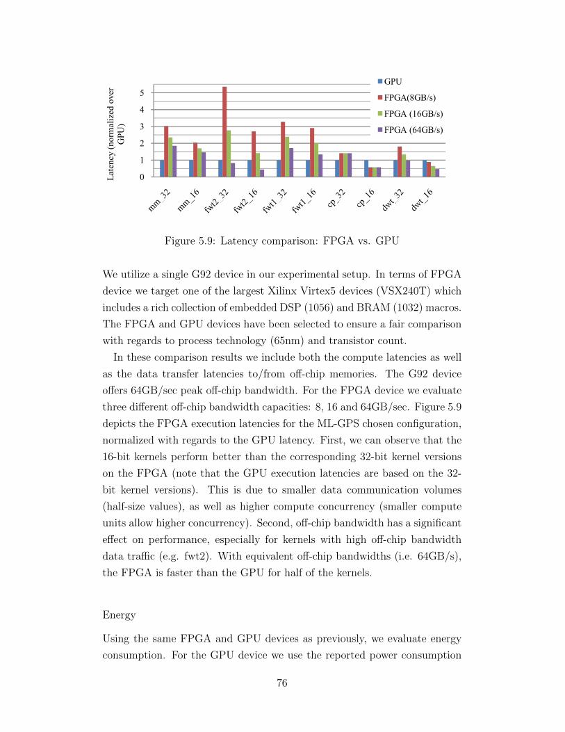
0
1
2
3
4
5
Late
ncy
(nor
mal
ized
ove
r G
PU)
GPU
FPGA(8GB/s)
FPGA (16GB/s)
FPGA (64GB/s)
0
1
2
3
4
5
Late
ncy
(nor
mal
ized
ove
r G
PU)
GPU
FPGA(8GB/s)
FPGA (16GB/s)
FPGA (64GB/s)
Figure 5.9: Latency comparison: FPGA vs. GPU
We utilize a single G92 device in our experimental setup. In terms of FPGA
device we target one of the largest Xilinx Virtex5 devices (VSX240T) which
includes a rich collection of embedded DSP (1056) and BRAM (1032) macros.
The FPGA and GPU devices have been selected to ensure a fair comparison
with regards to process technology (65nm) and transistor count.
In these comparison results we include both the compute latencies as well
as the data transfer latencies to/from off-chip memories. The G92 device
offers 64GB/sec peak off-chip bandwidth. For the FPGA device we evaluate
three different off-chip bandwidth capacities: 8, 16 and 64GB/sec. Figure 5.9
depicts the FPGA execution latencies for the ML-GPS chosen configuration,
normalized with regards to the GPU latency. First, we can observe that the
16-bit kernels perform better than the corresponding 32-bit kernel versions
on the FPGA (note that the GPU execution latencies are based on the 32-
bit kernel versions). This is due to smaller data communication volumes
(half-size values), as well as higher compute concurrency (smaller compute
units allow higher concurrency). Second, off-chip bandwidth has a significant
effect on performance, especially for kernels with high off-chip bandwidth
data traffic (e.g. fwt2). With equivalent off-chip bandwidths (i.e. 64GB/s),
the FPGA is faster than the GPU for half of the kernels.
Energy
Using the same FPGA and GPU devices as previously, we evaluate energy
consumption. For the GPU device we use the reported power consumption
76
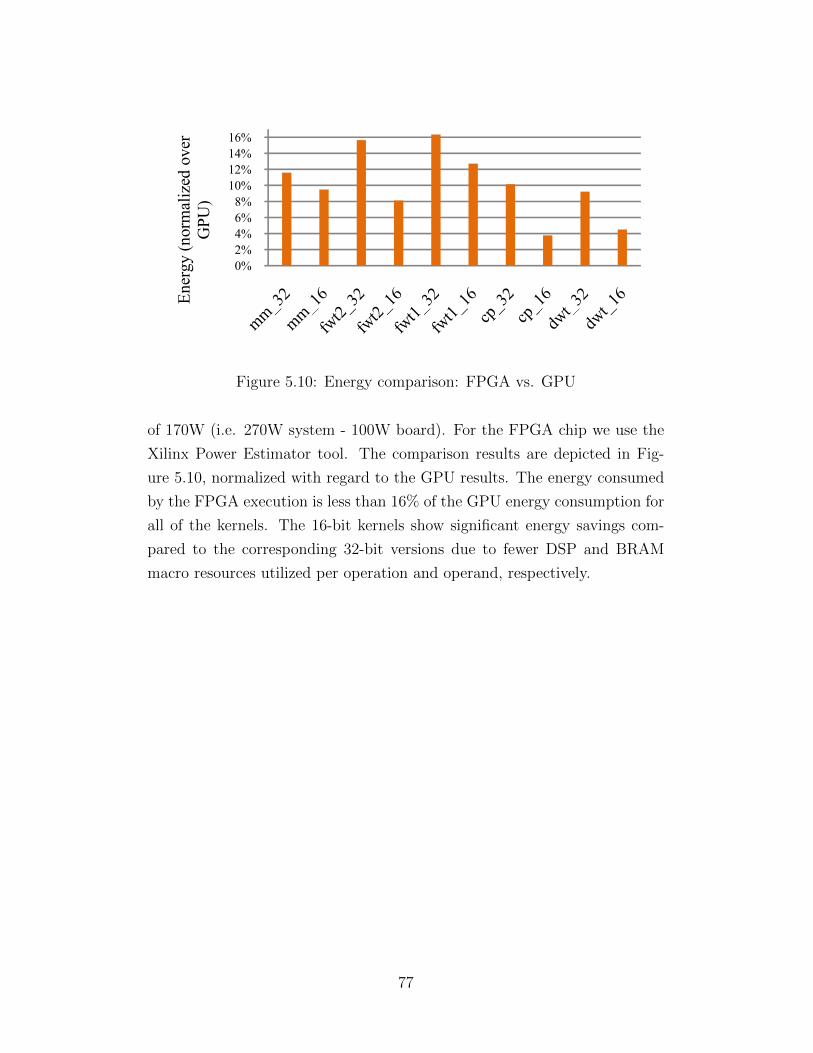
0%2%4%6%8%
10%12%14%16%
rgy
(nor
mal
ized
ove
r G
PU)
0%2%4%6%8%
10%12%14%16%
Ener
gy (n
orm
aliz
ed o
ver
GPU
)
Figure 5.10: Energy comparison: FPGA vs. GPU
of 170W (i.e. 270W system - 100W board). For the FPGA chip we use the
Xilinx Power Estimator tool. The comparison results are depicted in Fig-
ure 5.10, normalized with regard to the GPU results. The energy consumed
by the FPGA execution is less than 16% of the GPU energy consumption for
all of the kernels. The 16-bit kernels show significant energy savings com-
pared to the corresponding 32-bit versions due to fewer DSP and BRAM
macro resources utilized per operation and operand, respectively.
77
CHAPTER 6
THROUGHPUT-DRIVEN PARALLELISMSYNTHESIS (TDPS)
As discussed in previous chapters, heterogeneity in compute systems is be-
coming widespread due to the ever increasing need for massively parallel com-
puting at low power consumption. Programming simplicity and efficiency is
a prerequisite for leveraging the benefits of heterogeneous computing. Par-
allel programming models such as CUDA [42], OpenCL [43] and OpenACC
[71] are addressing this need by providing a homogeneous programming in-
terface which can efficiently represent and map parallelism onto throughput-
oriented processors with heterogeneous architectures. In Chapter 4 we pre-
sented our work on the FCUDA flow which enables mapping CUDA ker-
nels on FPGA devices. The use of homogeneous programming model across
heterogeneous compute architectures facilitates higher programming produc-
tivity but may not achieve good performance without device-specific code
tweaking. Maximizing performance on the target processor is dependent on
effectively expressing the application’s computation for the target architec-
ture. Restructuring the application’s computation organization and applying
architecture-specific optimizations may be necessary to fully take advantage
of the performance potential of throughput-oriented architectures. Previous
studies with GPU architectures have shown that poorly optimized code can
lead to dramatic performance degradation [72]. Similarly, the performance
of custom accelerators implemented on FPGAs may be severely affected by
the application’s compute organization when using HLS-based flows (as in
FCUDA).
In this chapter we describe a source-to-source code transformation frame-
work that leverages throughput-driven code restructuring techniques to en-
able automatic performance porting of CUDA kernels onto FPGAs. In
CUDA, as in other parallel programming models supporting heterogeneous
compute architectures (e.g. OpenCL [43]), the programmer has explicit con-
trol over the data memory spaces as well as how computation is distributed
78
across cores and how threads and cores share data and synchronize during
data accesses. Thus, CUDA kernels designed for the GPU architecture may
be structured inefficiently for reconfigurable devices. The throughput-driven
parallelism synthesis (TDPS) framework, proposed in this work, facilitates ef-
ficient computation mapping onto the reconfigurable fabric and performance
porting through kernel analysis and generation of a hierarchical region graph
(HRG) representation. Restructuring leverages a wide range of transforma-
tions including code motions, synchronization elimination (through array re-
naming), data communication elimination (through re-materialization), and
idle thread elimination (through control flow fusion and loop interchange).
Since data storage and communication play a critical role in performance
of massively threaded CUDA kernels, the proposed flow employs advanced
dataflow and symbolic analysis techniques to facilitate efficient data han-
dling. Graph coloring in tandem with throughput estimation techniques is
used to optimize kernel data structure allocation and utilization of on-chip
memories. The TDPS framework orchestrates all these kernel transforma-
tions and optimizations to generate high-throughput custom accelerators on
the reconfigurable architecture. We have integrated the TDPS framework
in the FCUDA flow (Chapter 4) in order to alleviate the programmer from
the time-consuming and error-prone code annotation and restructuring work.
Our experimental study shows that the proposed flow achieves highly effi-
cient (i.e. no manual code tweaking) and high-throughput (similar or better
to manual porting quality) performance porting of GPU-optimized CUDA
kernels on the FPGA device.
6.1 Background and Motivation
As we discussed in Section 4.1.1, CUDA supports a SIMT (single instruction,
multiple threads) parallel programming model which uses relaxed memory
consistency with respect to memory reference ordering among threads. Ex-
plicit synchronization directives are included in the model to enforce opera-
tion ordering and thread synchronization. For example, the __syncthreads()
directive (lines 3,5,8,18 in Listing 6.1) enforces thread synchronization at the
level of cooperative thread arrays (CTAs) by preventing threads to proceed
further until all CTA threads have finished executing the instructions before
79
the directive. In Section 4.2 we described the SIMT-to-C (S2C) translation
philosophy for porting CUDA kernels onto non-GPU architectures such as
multicore CPUs [73] and FPGAs [74]. A common characteristic of these
S2C compilation schemes is explicit representation of threads as loops that
iterate across the CTA’s thread index (tIDX) values (hereafter referred as
tIDX-loops). Thread synchronization is enforced through loop fission (e.g.
tIDX-loop in line 1 of Listing 6.1 is split into 5 loops in Listing 6.2 - lines 1,
3, 5, 8 and 12), loop interchange (e.g. loops in lines 11, 12 in Listing 6.2) and
variable privatization (e.g. d0 in line 4, Listing 6.2) transformations. More-
over, tIDX-loop unrolling in tandem with vector loads/stores (for fixed CPU
architectures but also custom cores (CC) on FPGAs) may be used to exploit
the CUDA thread parallelism in the kernel. In addition, the FCUDA com-
pilation scheme applies decomposition of the kernel into data computation
(COMPUTE) and communication (TRANSFER) tasks. Task decomposition
is essential in optimizing the CTA execution latency on the reconfigurable
fabric. Decomposing all off-chip memory references across CTA threads into
TRANSFER tasks, for example, can facilitate organization of coalesced ac-
cesses into burst transfers. Hence, off-chip memory bandwidth can be op-
timized and address computation overhead can be eliminated. COMPUTE
tasks can also benefit from decomposition as multiple thread computation se-
quences are executed independently from long-latency off-chip accesses. The
implementation of kernel decomposition described in Section 4.2 is based on
user-injected annotations that assist the compiler through the transformation
of the kernel into COMPUTE and TRANSFER tasks.
6.1.1 Throughput-Oriented SIMT Porting onto FPGA
In this chapter we adopt the COMPUTE/TRANSFER kernel decomposition
philosophy, but propose a new compilation flow that eliminates the need for
user-injected annotations in the kernel code. The proposed flow leverages
sophisticated analysis and transformation techniques to identify the kernel
tasks and re-structure them so as to optimize execution throughput on the
FPGA architecture. We will use the Nvidia SDK kernel for discreet wavelet
transforms (DWT) as a running example in the rest of this chapter to moti-
vate the importance of throughput-driven parallelism synthesis (TDPS) im-
80
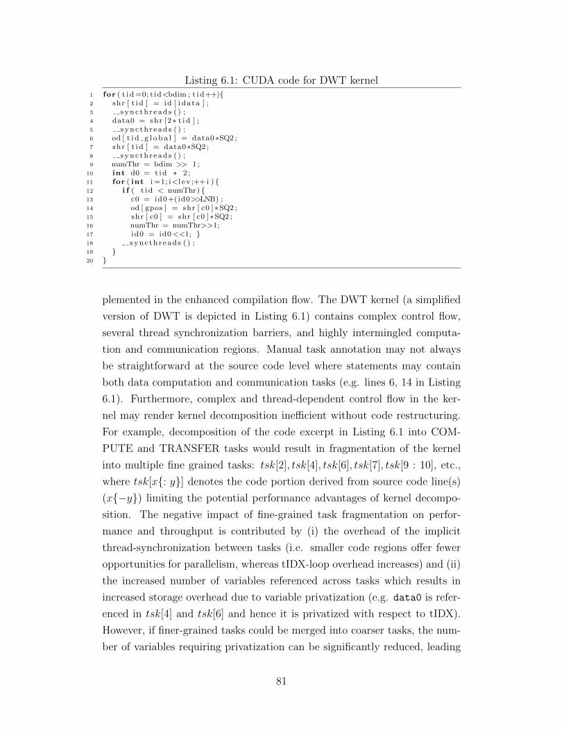
Listing 6.1: CUDA code for DWT kernel1 for ( t i d =0; t id<bdim ; t i d++){2 shr [ t i d ] = id [ ida ta ] ;3 sync th r ead s ( ) ;4 data0 = shr [2∗ t i d ] ;5 sync th r ead s ( ) ;6 od [ t i d g l o b a l ] = data0∗SQ2 ;7 shr [ t i d ] = data0∗SQ2 ;8 sync th r ead s ( ) ;9 numThr = bdim >> 1 ;
10 int d0 = t i d ∗ 2 ;11 for ( int i =1; i<l e v ;++ i ) {12 i f ( t i d < numThr) {13 c0 = id0+(id0>>LNB) ;14 od [ gpos ] = shr [ c0 ]∗SQ2 ;15 shr [ c0 ] = shr [ c0 ]∗SQ2 ;16 numThr = numThr>>1;17 id0 = id0<<1; }18 sync th r ead s ( ) ;19 }20 }
plemented in the enhanced compilation flow. The DWT kernel (a simplified
version of DWT is depicted in Listing 6.1) contains complex control flow,
several thread synchronization barriers, and highly intermingled computa-
tion and communication regions. Manual task annotation may not always
be straightforward at the source code level where statements may contain
both data computation and communication tasks (e.g. lines 6, 14 in Listing
6.1). Furthermore, complex and thread-dependent control flow in the ker-
nel may render kernel decomposition inefficient without code restructuring.
For example, decomposition of the code excerpt in Listing 6.1 into COM-
PUTE and TRANSFER tasks would result in fragmentation of the kernel
into multiple fine grained tasks: tsk[2], tsk[4], tsk[6], tsk[7], tsk[9 : 10], etc.,
where tsk[x{: y}] denotes the code portion derived from source code line(s)
(x{−y}) limiting the potential performance advantages of kernel decompo-
sition. The negative impact of fine-grained task fragmentation on perfor-
mance and throughput is contributed by (i) the overhead of the implicit
thread-synchronization between tasks (i.e. smaller code regions offer fewer
opportunities for parallelism, whereas tIDX-loop overhead increases) and (ii)
the increased number of variables referenced across tasks which results in
increased storage overhead due to variable privatization (e.g. data0 is refer-
enced in tsk[4] and tsk[6] and hence it is privatized with respect to tIDX).
However, if finer-grained tasks could be merged into coarser tasks, the num-
ber of variables requiring privatization can be significantly reduced, leading
81
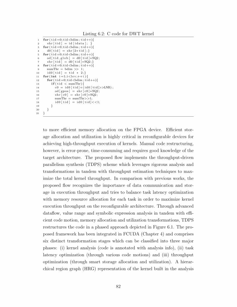
Listing 6.2: C code for DWT kernel1 for ( t i d =0; t id<bdim ; t i d++){2 shr [ t i d ] = id [ ida ta ] ; }3 for ( t i d =0; t id<bdim ; t i d++){4 d0 [ t i d ] = shr [ 2∗ t i d ] ; }5 for ( t i d =0; t id<bdim ; t i d++){6 od [ t i d g l o b ] = d0 [ t i d ]∗SQ2 ;7 shr [ t i d ] = d0 [ t i d ]∗SQ2 ;}8 for ( t i d =0; t id<bdim ; t i d++){9 numThr = bdim >> 1 ;
10 id0 [ t i d ] = t i d ∗ 2 ;}11 for ( int i =1; i<l e v ;++ i ) {12 for ( t i d =0; t id<bdim ; t i d++){13 i f ( t i d < numThr) {14 c0 = id0 [ t i d ]+( id0 [ t i d ]>>LNB) ;15 od [ gpos ] = shr [ c0 ]∗SQ2 ;16 shr [ c0 ] = shr [ c0 ]∗SQ2 ;17 numThr = numThr>>1;18 id0 [ t i d ] = id0 [ t i d ]<<1;19 }20 }21 }
to more efficient memory allocation on the FPGA device. Efficient stor-
age allocation and utilization is highly critical in reconfigurable devices for
achieving high-throughput execution of kernels. Manual code restructuring,
however, is error-prone, time-consuming and requires good knowledge of the
target architecture. The proposed flow implements the throughput-driven
parallelism synthesis (TDPS) scheme which leverages rigorous analysis and
transformations in tandem with throughput estimation techniques to max-
imize the total kernel throughput. In comparison with previous works, the
proposed flow recognizes the importance of data communication and stor-
age in execution throughput and tries to balance task latency optimization
with memory resource allocation for each task in order to maximize kernel
execution throughput on the reconfigurable architecture. Through advanced
dataflow, value range and symbolic expression analysis in tandem with effi-
cient code motion, memory allocation and utilization transformations, TDPS
restructures the code in a phased approach depicted in Figure 6.1. The pro-
posed framework has been integrated in FCUDA (Chapter 4) and comprises
six distinct transformation stages which can be classified into three major
phases: (i) kernel analysis (code is annotated with analysis info), (ii) task
latency optimization (through various code motions) and (iii) throughput
optimization (through smart storage allocation and utilization). A hierar-
chical region graph (HRG) representation of the kernel built in the analysis
82
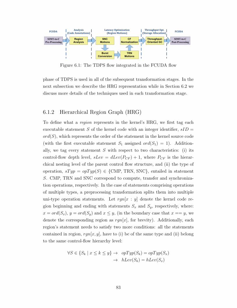
Region Analysis
SNCMotions
Burst Conversion
TRN Motions
CF Normalization
SIMT-to-CPre-Processing
Throughput-Oriented GC
SIMT-to-CPost-Processing
Analysis(Code Annotations)
Latency Optimization(Region Motions)
Throughput Opt. (Storage Allocation)
FCUDA FCUDA
Figure 6.1: The TDPS flow integrated in the FCUDA flow
phase of TDPS is used in all of the subsequent transformation stages. In the
next subsection we describe the HRG representation while in Section 6.2 we
discuss more details of the techniques used in each transformation stage.
6.1.2 Hierarchical Region Graph (HRG)
To define what a region represents in the kernel’s HRG, we first tag each
executable statement S of the kernel code with an integer identifier, sID =
ord(S), which represents the order of the statement in the kernel source code
(with the first executable statement S1 assigned ord(S1) = 1). Addition-
ally, we tag every statement S with respect to two characteristics: (i) its
control-flow depth level, sLev = dLev(PCF ) + 1, where PCF is the hierar-
chical nesting level of the parent control flow structure, and (ii) the type of
operation, sTyp = opTyp(S) ∈ {CMP, TRN, SNC}, entailed in statement
S. CMP, TRN and SNC correspond to compute, transfer and synchroniza-
tion operations, respectively. In the case of statements comprising operations
of multiple types, a preprocessing transformation splits them into multiple
uni-type operation statements. Let rgn[x : y] denote the kernel code re-
gion beginning and ending with statements Sx and Sy, respectively, where:
x = ord(Sx), y = ord(Sy) and x ≤ y, (in the boundary case that x == y, we
denote the corresponding region as rgn[x], for brevity). Additionally, each
region’s statement needs to satisfy two more conditions: all the statements
contained in region, rgn[x, y], have to (i) be of the same type and (ii) belong
to the same control-flow hierarchy level:
∀S ∈ {Sk | x ≤ k ≤ y} → opTyp(Sk) = opTyp(Sx)
→ hLev(Sk) = hLev(Sx)
83
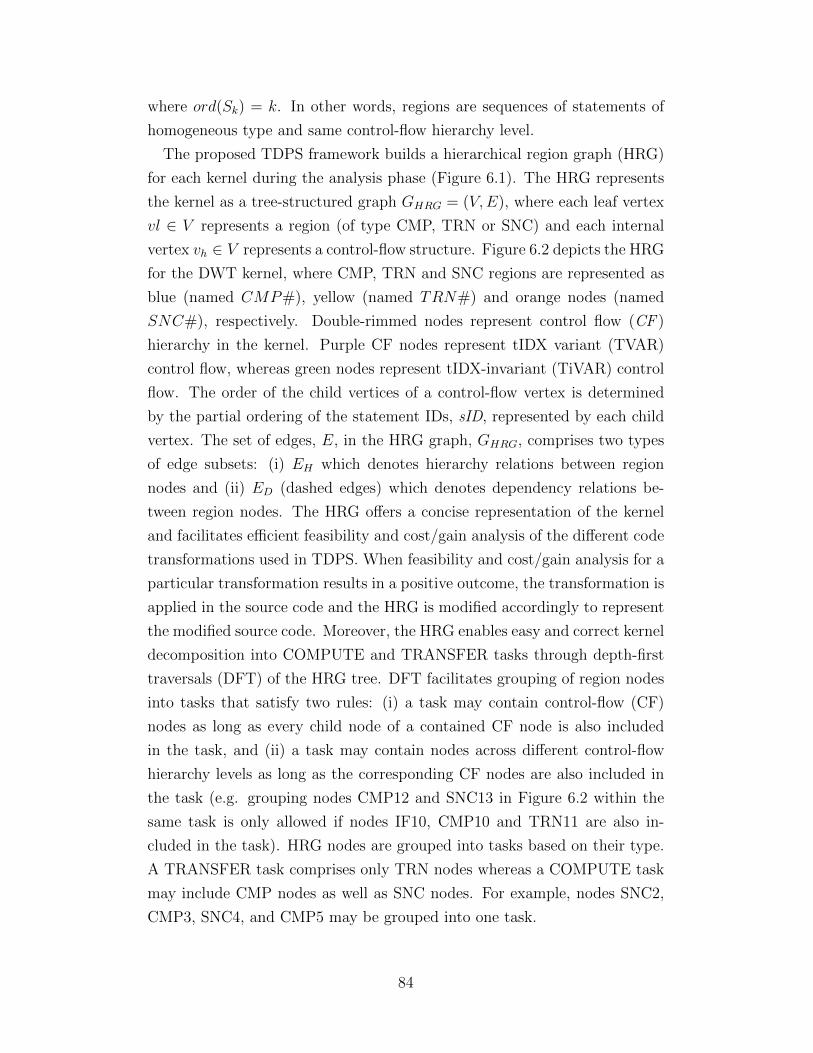
where ord(Sk) = k. In other words, regions are sequences of statements of
homogeneous type and same control-flow hierarchy level.
The proposed TDPS framework builds a hierarchical region graph (HRG)
for each kernel during the analysis phase (Figure 6.1). The HRG represents
the kernel as a tree-structured graph GHRG = (V,E), where each leaf vertex
vl ∈ V represents a region (of type CMP, TRN or SNC) and each internal
vertex vh ∈ V represents a control-flow structure. Figure 6.2 depicts the HRG
for the DWT kernel, where CMP, TRN and SNC regions are represented as
blue (named CMP#), yellow (named TRN#) and orange nodes (named
SNC#), respectively. Double-rimmed nodes represent control flow (CF )
hierarchy in the kernel. Purple CF nodes represent tIDX variant (TVAR)
control flow, whereas green nodes represent tIDX-invariant (TiVAR) control
flow. The order of the child vertices of a control-flow vertex is determined
by the partial ordering of the statement IDs, sID, represented by each child
vertex. The set of edges, E, in the HRG graph, GHRG, comprises two types
of edge subsets: (i) EH which denotes hierarchy relations between region
nodes and (ii) ED (dashed edges) which denotes dependency relations be-
tween region nodes. The HRG offers a concise representation of the kernel
and facilitates efficient feasibility and cost/gain analysis of the different code
transformations used in TDPS. When feasibility and cost/gain analysis for a
particular transformation results in a positive outcome, the transformation is
applied in the source code and the HRG is modified accordingly to represent
the modified source code. Moreover, the HRG enables easy and correct kernel
decomposition into COMPUTE and TRANSFER tasks through depth-first
traversals (DFT) of the HRG tree. DFT facilitates grouping of region nodes
into tasks that satisfy two rules: (i) a task may contain control-flow (CF)
nodes as long as every child node of a contained CF node is also included
in the task, and (ii) a task may contain nodes across different control-flow
hierarchy levels as long as the corresponding CF nodes are also included in
the task (e.g. grouping nodes CMP12 and SNC13 in Figure 6.2 within the
same task is only allowed if nodes IF10, CMP10 and TRN11 are also in-
cluded in the task). HRG nodes are grouped into tasks based on their type.
A TRANSFER task comprises only TRN nodes whereas a COMPUTE task
may include CMP nodes as well as SNC nodes. For example, nodes SNC2,
CMP3, SNC4, and CMP5 may be grouped into one task.
84
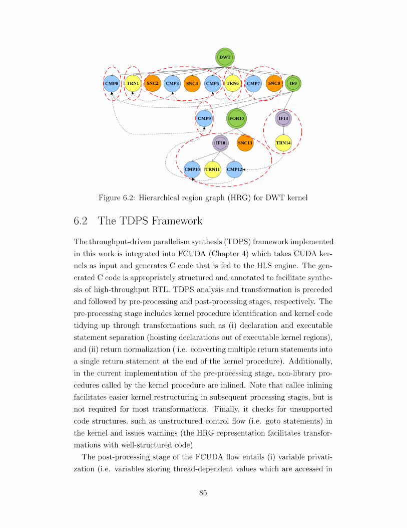
DWT
IF9CMP0 TRN1 SNC2 CMP3 SNC4 CMP5 TRN6 CMP7 SNC8
CMP9
SNC13
CMP10 TRN11 CMP12
TRN14
IF14
IF10
FOR10
Figure 6.2: Hierarchical region graph (HRG) for DWT kernel
6.2 The TDPS Framework
The throughput-driven parallelism synthesis (TDPS) framework implemented
in this work is integrated into FCUDA (Chapter 4) which takes CUDA ker-
nels as input and generates C code that is fed to the HLS engine. The gen-
erated C code is appropriately structured and annotated to facilitate synthe-
sis of high-throughput RTL. TDPS analysis and transformation is preceded
and followed by pre-processing and post-processing stages, respectively. The
pre-processing stage includes kernel procedure identification and kernel code
tidying up through transformations such as (i) declaration and executable
statement separation (hoisting declarations out of executable kernel regions),
and (ii) return normalization ( i.e. converting multiple return statements into
a single return statement at the end of the kernel procedure). Additionally,
in the current implementation of the pre-processing stage, non-library pro-
cedures called by the kernel procedure are inlined. Note that callee inlining
facilitates easier kernel restructuring in subsequent processing stages, but is
not required for most transformations. Finally, it checks for unsupported
code structures, such as unstructured control flow (i.e. goto statements) in
the kernel and issues warnings (the HRG representation facilitates transfor-
mations with well-structured code).
The post-processing stage of the FCUDA flow entails (i) variable privati-
zation (i.e. variables storing thread-dependent values which are accessed in
85
different regions of the HRG may need privatization with respect to threads),
(ii) kernel task outlining (i.e. the tasks formed by the TDPS framework are
outlined into separate task procedures), (iii) intra-CTA parallelism extraction
(i.e. thread parallelization through tIDX-loop unrolling and on-chip memory
banking), and (iv) inter-CTA parallelism extraction (through replication of
the task procedure calls, which results in multi-CC RTL). Pre-processing and
post-processing transformations are based on ideas discussed in earlier works
[74, 73, 48] and thus will not be further described here.
6.2.1 TDPS Framework Overview
The TDPS framework initially carries out an analysis phase which is imple-
mented by the region analysis stage (Figure 6.1). This stage performs region
identification and annotation in the kernel code and builds the HRG (Figure
6.2). Furthermore, each statement is annotated with region and referenced
variable information which is leveraged in later stages. The subsequent four
stages compose the latency optimization phase which is based on different
types of region motions. The first stage of this phase implements thread syn-
chronization optimization through SNC region motions. Data dependence
analysis and synchronization cost estimation on the FPGA architecture are
used to determine opportunities for profitable motions of SNC regions. Shift-
ing SNC regions within the HRG can enable merging of fine-grained CM-
P/TRN regions into coarser ones for higher kernel execution efficiency on
the reconfigurable fabric. In the burst conversion stage, CMP regions which
entail address computation for TRN regions are analyzed to determine the
feasibility of converting individual thread transfers into bursts. In case of
positive analysis outcome, the corresponding CMP and TRN regions are com-
bined into new TRN regions implementing the burst transfer. Subsequently,
the TRN region motions stage identifies the feasibility and potential benefits
from reorganizing TRN regions within the HRG sub-tree rooted at the parent
control-flow node. Data dependence and cost/gain analyses are leveraged to
identify new beneficial region orderings. The last stage of the latency op-
timization phase implements control-flow normalization by considering the
possibility of splitting control flow (CF) sub-trees with heterogeneous child
regions into separate CF sub-trees of single-type child regions. Addition-
86
ally, the CF normalization stage entails sub-tree motions in the HRG, using
feasibility and cost/gain analyses similarly to the TRN motion stage.
After latency optimization at the custom core (CC) level, the throughput
optimization phase takes place (Figure 6.1). This phase considers through-
put optimization at the device level by analyzing the tradeoffs between CTA
latency and CTA throughput with respect to on-chip memory allocation. A
graph coloring algorithm is used to efficiently find a throughput-optimized
mapping of data structures onto FPGA BRAMs. Moreover, an efficient
throughput optimization algorithm considers region reordering opportunities
that facilitate enhanced overall throughput.
6.2.2 Analysis Phase
Region analysis identifies the CMP, TRN and SNC regions in the kernel and
annotates each statement with region and thread-dependence information.
The annotated information is also used for the generation of the HRG. The
analysis process is carried out as a sequence of six steps: (A1 ) Locate global
memory accesses, (A2 ) Normalize mixed-type statement, (A3 ) Build Def-
Use chains [75], (A4 ) Find tIDX-variant (TVAR) statements, (A5 ) Annotate
TVAR statements, and (A6 ) Build the kernel’s HRG. Initially global mem-
ory variables are identified and all global memory references are collected in
step A1. Global memory variables include CUDA __constant__ variables
and kernel procedure parameters of pointer type, as well as all of their kernel-
defined aliases through pointer arithmetic expressions. During step A2, ker-
nel statements are scanned to find mixed-type statements, i.e. statements
entailing both CMP and TRN operations. Each such statement is converted
into separate single-typed CMP and TRN statements. Once computation
and communication logic are decomposed at the statement level, dataflow
analysis is used to build Def-Use chains (step A3 ). Def-Use chains facilitate
tIDX-variant (TVAR) variable and statement identification (i.e. variables/s-
tatements that store/calculate tIDX-dependent values) during step A4 and
tagging during step A5. Finally the HRG is constructed in step A6 with the
help of the analysis information annotated on the kernel statements. Each
node in the HRG (Figure 6.2) which corresponds to a kernel region is as-
signed a region identifier, rID, that is used to create a partial ordering of all
87
the CMP, TRN and SNC regions (rID partial ordering is determined through
depth-first traversal of the kernel code). Control-flow nodes are assigned the
smallest rID of the region nodes in their subtree (e.g. CF node IF9, is
tagged with the smallest rID of its subtree nodes: rIDIF9 = rIDCMP9 = 9).
Moreover, the HRG is annotated with inter-region dependence information
(dashed black arrows in Figure 6.2) based on the Def-Use analysis data.
6.2.3 Latency Optimization Phase
The latency optimization phase of TDPS comprises different region motion
stages which aim to eliminate the execution latency overhead originating
from excessive (i) CMP and TRN interleaving, and (ii) synchronization di-
rectives. Hence, the goal of the transformations applied in this phase is to
reduce CTA execution latency through HRG reorganization so as to avoid
fragmentation of the CTA into multiple fine-grained tasks. For example,
the initial organization of the DWT HRG (Figure 6.2) has eight interleaved
tasks (marked with the dashed red circles). Since each task is outlined in a
separate task procedure in the FCUDA flow, task boundaries represent im-
plicit synchronization points (ISPs) imposing synchronization overhead and
eliminating ILP extraction opportunities across tasks. Apart from task la-
tency, HRG reorganization also affects resource storage. That is, multiple
fine-grained tasks result in additional TVAR variables being accessed across
ISPs. In the FCUDA flow this is dealt with by variable privatization with
respect to tIDX, which results in higher BRAM resource usage (e.g. vari-
ables d0 and id0 in Listing 6.1 are privatized after standard SIMT-to-C task
decomposition in Listing 6.2). The TDPS framework considers the impact
on BRAM allocation and tries to reorder and merge regions into fewer tasks
so as to reduce ISPs formed by task boundaries.
The HRG in tandem with the annotated Def-Use chain information plays
a critical role in region motion feasibility analysis and cost/gain estimation
during the transformation stages in this phase. Each inter-region Def-Use
chain is characterized based on the type of variable it corresponds to as ei-
ther thread shared chain (TSC) or thread private chain (TPC). TSCs corre-
spond to chains related to __shared__ or global variables where inter-thread
dependence may require explicit synchronization between the definition re-
88
SNCx
SNCy
SNCp
SNCn
CMPrdef1def2
CMPvuse1def3
CMPsuse2use3
(CHN1: Desync.)
(CHN2: NA)
(CHN3: Sync.)
(a) Forward SNC sweep
SNCx
SNCy
SNCp
SNCn
CMPrdef1def2
CMPvuse1def3
CMPsuse2use3
(CHN1: Sync.)
(CHN2: NA)
(CHN3: Desync.)
(b) Backward SNC sweep
Figure 6.3: SNC region motions
gion and the use region (e.g. the chain between the definition and use of
__shared__ variable shr in lines 2, 4 of Listing 6.1, respectively; also rep-
resented with dependence edge between TRN1 and CMP3 in Figure 6.2).
TPCs, on the other hand, correspond to thread-private variables and are not
affected by CTA synchronization directives. Nonetheless, synchronization
might affect the storage allocation for private thread chains, as discussed
earlier. Hence, TSCs affect the feasibility of region motions, whereas TPCs
affect the cost/gain estimation analysis of region motions. There are three
possible effects that region motions may have on Def-Use chains: (i) Desyn-
chronization (DSYNC), (ii) Synchronization (SYNC), or (iii) Not affected
(NA). Desynchronization happens in the case that the explicit or implicit
synchronization points between source and sink regions of a chain are re-
moved (e.g. in the case of SNC region motions, if SNCp is shifted to SNCn
in Figure 6.3(a), then chain CHN1 between def1 and use1 is desynchronized).
Correspondingly, CHN3 between def3 and use3 is synchronized for the same
SNCp → SNCn motion, whereas CHN2 is not affected by this region mo-
tion. Determining which case a region motion corresponds to, is based on
the partial ordering enforced by the region identifiers assigned to the involved
regions (see Section 6.2.2).
As mentioned earlier, TSCs may affect the feasibility of a region motion.
The feasibility of a region motion with respect to a TSC is determined by
the motion effect on the chain (i.e. DSYNC, SYNC or NA, as characterized
89
above) in combination with the value of its dependence distance vector [76].
Specifically, in case of SYNC or NA motion effects on the TSC, feasibility is
positive regardless of the dependence vector distance (e.g. CHN2 and CHN3
in Figure 6.3(a)). However, in case of DSYNC motion effect on the TSC,
the dependence distance vector needs to be examined in order to determine
feasibility. We leverage the work in [77] and extend it by applying dependence
distance vectors in determining region motion feasibility. Specifically, the
authors in [77] show that it is feasible to remove implicit synchronization
points (ISPs) between the source and sink of a Def-Use chain as long as one
of the following rules holds with respect to the chain’s distance dependence
vector v:
• v[0] == 0
• v[0] < 0 ∧ v[1 : (|v| − 1)] == 0
• v[0] == v[i] : i ∈ [1 : (|v| − 1)] ∧ v[1 : i] == 0
where v[0] corresponds to the outer loop index (i.e. tIDX) and v[0] < 0 de-
notes an inter-thread data dependence. For the purpose of determining the
feasibility of a region motion we apply this test also for explicit synchroniza-
tion points (ESPs). To evaluate the distance vector we leverage symbolic
analysis ([75]) in combination with range analysis ([78, 66]) and array depen-
dence analysis ([75, 76]). If none of the conditions can be proven, feasibility
is not confirmed and the corresponding region motion is rejected. In the
following subsections we discuss further details of the transformation stages
in the latency optimization phase of TDPS.
SNC Region Motions
This stage identifies feasible SNC motions that facilitate region merging.
Region merging helps coarsen kernel tasks, reduce barrier and tIDX-loop
overhead and reduce task latency through more ILP extraction within larger
tasks. SNC region shifts are only considered within their current scope (i.e.
SNC nodes are not shifted across different HRG tree levels). The SNC mo-
tions stage involves four main steps: (SM1 ) Collect all SNC regions, (SM2 )
Get feasible destinations, (SM3 ) Estimate motion cost/gain, and (SM4 ) Per-
form motion. Initially SNC regions are collected (step SM1 ) and ordered
90
with respect to their region identifier, rID. For each synchronization re-
gion, SNCp, destination location candidates in the current HRG level are
examined to identify the feasible ones (step SM2 ). Candidate destination
locations are explored in two sweeps of the corresponding HRG level: a for-
ward (Figure 6.3(a)) and a backward sweep (Figure 6.3(b)) starting from the
original location of SNCp in the HRG. Let us use rIDSNCp = p, of region
SNCp to denote its original location (note that region IDs provide partial
ordering of HRG nodes). During a sweep, the candidate destination location
is the location corresponding to one region hop in the corresponding sweep
direction. The sweep ends when the boundary of the level is reached or a
non-feasible destination is encountered. Feasibility is tested as described in
Section 6.2.3 with respect to all TSCs having source region ID, r : r < p,
and sink region ID, v : v > p and the new region ID, n, of destination lo-
cation, SNCn, satisfies the following condition: n > v, for forward sweeps
(Figure 6.3(a)), or n < v, for backward sweeps (Figure 6.3(b)). For each
shift during the sweep, only additional TSCs need to be tested with regard
to fulfilling the aforementioned feasibility conditions. The sweep ends when
the new candidate destination location, SNCn, breaks feasibility for a TSC.
Each of the feasible destinations identified is evaluated (step SM3 ) with
regard to the following factors:
• De-synchronized TPCs gain
• Synchronized TPCs cost
• Explicit synchronization point (ESP) elimination gain
• Implicit synchronization point (ISP) overhead cost
Note that ESP elimination may happen if the candidate destination location
has a SNC region neighbor. For example, SNC motion application on the
DWT HRG results in elimination of the SNC4 region (Figure 6.4). On the
other hand, ISP overhead may result from shifting the SNCp region among
regions that could potentially be merged within a single task (e.g. two neigh-
boring CMP regions). Finally, a destination location for SNCp is selected
based on evaluation of all the candidate destinations. Then, the correspond-
ing SNC region motion is implemented in the code and represented in the
HRG (step SM4 ).
91
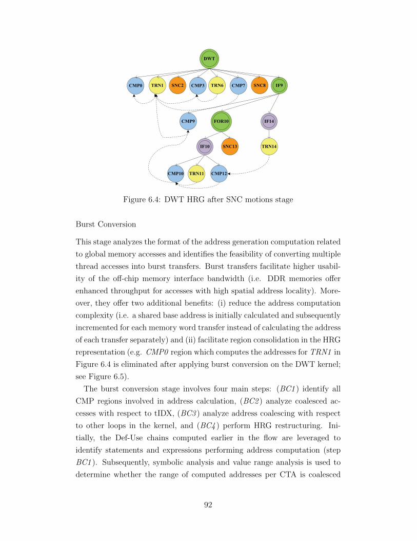
DWT
IF9CMP0 TRN1 SNC2 CMP3 TRN6 CMP7 SNC8
CMP9
SNC13
CMP10 TRN11 CMP12
TRN14
IF14
IF10
FOR10
Figure 6.4: DWT HRG after SNC motions stage
Burst Conversion
This stage analyzes the format of the address generation computation related
to global memory accesses and identifies the feasibility of converting multiple
thread accesses into burst transfers. Burst transfers facilitate higher usabil-
ity of the off-chip memory interface bandwidth (i.e. DDR memories offer
enhanced throughput for accesses with high spatial address locality). More-
over, they offer two additional benefits: (i) reduce the address computation
complexity (i.e. a shared base address is initially calculated and subsequently
incremented for each memory word transfer instead of calculating the address
of each transfer separately) and (ii) facilitate region consolidation in the HRG
representation (e.g. CMP0 region which computes the addresses for TRN1 in
Figure 6.4 is eliminated after applying burst conversion on the DWT kernel;
see Figure 6.5).
The burst conversion stage involves four main steps: (BC1 ) identify all
CMP regions involved in address calculation, (BC2 ) analyze coalesced ac-
cesses with respect to tIDX, (BC3 ) analyze address coalescing with respect
to other loops in the kernel, and (BC4 ) perform HRG restructuring. Ini-
tially, the Def-Use chains computed earlier in the flow are leveraged to
identify statements and expressions performing address computation (step
BC1 ). Subsequently, symbolic analysis and value range analysis is used to
determine whether the range of computed addresses per CTA is coalesced
92
with respect to tIDX. In particular, forward substitution is used to derive
the address calculation expression, EA. Then, the tIDX variant (TVAR)
analysis performed during region analysis stage is used to decompose the
expression into a TVAR part, ETV AR, and a tIDX invariant part, ET iV AR:
EA = ETV AR + ET iV AR. Symbolic and range analyses are used to examine
the ETV AR expression and determine whether memory accesses are coalesced
in piecewise ranges, [si : ei], of the tIDX domain. If such piecewise domain
ranges can be identified, their maximum range value is returned. Otherwise,
a negative value is returned to signify the infeasibility of static conversion
of memory transfers into bursts. Subsequently, a similar analysis of the
address calculation expressions is carried out to identify coalescing opportu-
nities across piecewise ranges of non tIDX-loops (step BC3 ). Any additional
piecewise ranges found are used to extend the tIDX piecewise ranges identi-
fied previously (step BC2 ).
Finally, during the last step of this stage, the address computation analysis
results are utilized to perform any required HRG modifications. In the case of
statically identified coalesced address ranges, individual thread accesses are
converted into memcpy calls where ET iNV serves as the source/destination
address and the size of the piecewise address range, [si : ei], as the transfer
length. memcpy calls are subsequently transformed into DMA-based bursts
by the high-level synthesis engine. In the case that no address ranges are
returned by static analysis, address computations are kept within CMP re-
gions and computed addresses are stored for use by the corresponding TRN
regions. Moreover, the noncoalesced TRN regions are annotated so as to be
interfaced during the post-processing phase of FCUDA to a dynamic data co-
alescing module. This module coalesces temporally and spatially neighboring
accesses into short data blocks during reads/writes to off-chip memory. Fig-
ure 6.6 shows a high-level overview of the dynamic memory access coalescing
module.
TRN Region Motions
This transformation stage performs TRN region motions within their current
scope (i.e. TRN nodes are not shifted across different HRG tree levels). In
particular, TRN-Read (TRN-R) regions (i.e. off-chip to on-chip data trans-
fers) are shifted toward the beginning of the HRG level, while TRN-Write
93
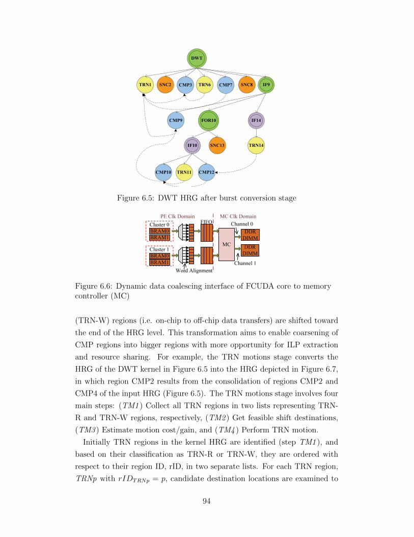
DWT
IF9TRN1 SNC2 CMP3 TRN6 CMP7 SNC8
CMP9
SNC13
CMP10 TRN11 CMP12
TRN14
IF14
IF10
FOR10
Figure 6.5: DWT HRG after burst conversion stage
Cluster 1BRAM0BRAM1
Cluster 0BRAM0BRAM1
MC
FIFO
DDR DIMM
PE Clk Domain MC Clk DomainChannel 0
Channel 1Word Alignment
DDR DIMM
Figure 6.6: Dynamic data coalescing interface of FCUDA core to memorycontroller (MC)
(TRN-W) regions (i.e. on-chip to off-chip data transfers) are shifted toward
the end of the HRG level. This transformation aims to enable coarsening of
CMP regions into bigger regions with more opportunity for ILP extraction
and resource sharing. For example, the TRN motions stage converts the
HRG of the DWT kernel in Figure 6.5 into the HRG depicted in Figure 6.7,
in which region CMP2 results from the consolidation of regions CMP2 and
CMP4 of the input HRG (Figure 6.5). The TRN motions stage involves four
main steps: (TM1 ) Collect all TRN regions in two lists representing TRN-
R and TRN-W regions, respectively, (TM2 ) Get feasible shift destinations,
(TM3 ) Estimate motion cost/gain, and (TM4 ) Perform TRN motion.
Initially TRN regions in the kernel HRG are identified (step TM1 ), and
based on their classification as TRN-R or TRN-W, they are ordered with
respect to their region ID, rID, in two separate lists. For each TRN region,
TRNp with rIDTRNp = p, candidate destination locations are examined to
94
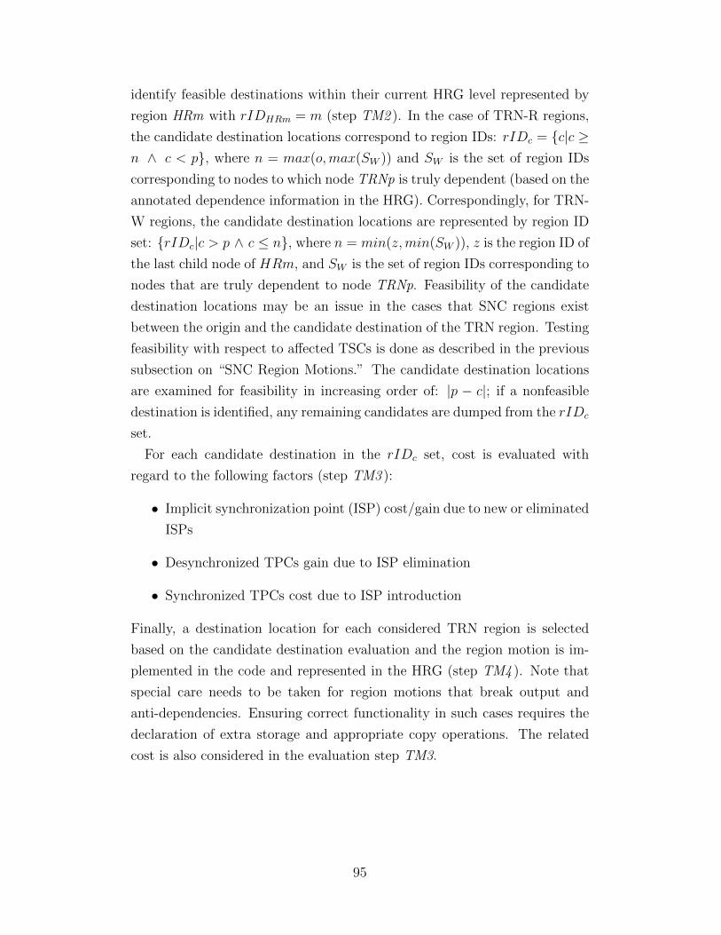
identify feasible destinations within their current HRG level represented by
region HRm with rIDHRm = m (step TM2 ). In the case of TRN-R regions,
the candidate destination locations correspond to region IDs: rIDc = {c|c ≥n ∧ c < p}, where n = max(o,max(SW )) and SW is the set of region IDs
corresponding to nodes to which node TRNp is truly dependent (based on the
annotated dependence information in the HRG). Correspondingly, for TRN-
W regions, the candidate destination locations are represented by region ID
set: {rIDc|c > p ∧ c ≤ n}, where n = min(z,min(SW )), z is the region ID of
the last child node of HRm, and SW is the set of region IDs corresponding to
nodes that are truly dependent to node TRNp. Feasibility of the candidate
destination locations may be an issue in the cases that SNC regions exist
between the origin and the candidate destination of the TRN region. Testing
feasibility with respect to affected TSCs is done as described in the previous
subsection on “SNC Region Motions.” The candidate destination locations
are examined for feasibility in increasing order of: |p − c|; if a nonfeasible
destination is identified, any remaining candidates are dumped from the rIDc
set.
For each candidate destination in the rIDc set, cost is evaluated with
regard to the following factors (step TM3 ):
• Implicit synchronization point (ISP) cost/gain due to new or eliminated
ISPs
• Desynchronized TPCs gain due to ISP elimination
• Synchronized TPCs cost due to ISP introduction
Finally, a destination location for each considered TRN region is selected
based on the candidate destination evaluation and the region motion is im-
plemented in the code and represented in the HRG (step TM4 ). Note that
special care needs to be taken for region motions that break output and
anti-dependencies. Ensuring correct functionality in such cases requires the
declaration of extra storage and appropriate copy operations. The related
cost is also considered in the evaluation step TM3.
95
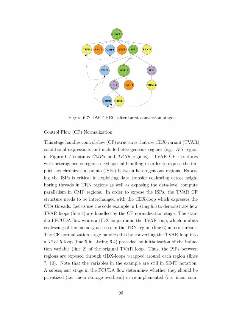
DWT
IF9TRN1 SNC2 CMP3 TRN15SNC8
CMP9
SNC13
CMP10 TRN11
TRN14
IF14
IF10
FOR10
Figure 6.7: DWT HRG after burst conversion stage
Control Flow (CF) Normalization
This stage handles control-flow (CF) structures that use tIDX-variant (TVAR)
conditional expressions and include heterogeneous regions (e.g. IF5 region
in Figure 6.7 contains CMP5 and TRN6 regions). TVAR CF structures
with heterogeneous regions need special handling in order to expose the im-
plicit synchronization points (ISPs) between heterogeneous regions. Expos-
ing the ISPs is critical in exploiting data transfer coalescing across neigh-
boring threads in TRN regions as well as exposing the data-level compute
parallelism in CMP regions. In order to expose the ISPs, the TVAR CF
structure needs to be interchanged with the tIDX-loop which expresses the
CTA threads. Let us use the code example in Listing 6.3 to demonstrate how
TVAR loops (line 4) are handled by the CF normalization stage. The stan-
dard FCUDA flow wraps a tIDX-loop around the TVAR loop, which inhibits
coalescing of the memory accesses in the TRN region (line 6) across threads.
The CF normalization stage handles this by converting the TVAR loop into
a TiVAR loop (line 5 in Listing 6.4) preceded by initialization of the induc-
tion variable (line 2) of the original TVAR loop. Thus, the ISPs between
regions are exposed through tIDX-loops wrapped around each region (lines
7, 10). Note that the variables in the example are still in SIMT notation.
A subsequent stage in the FCUDA flow determines whether they should be
privatized (i.e. incur storage overhead) or re-implemented (i.e. incur com-
96
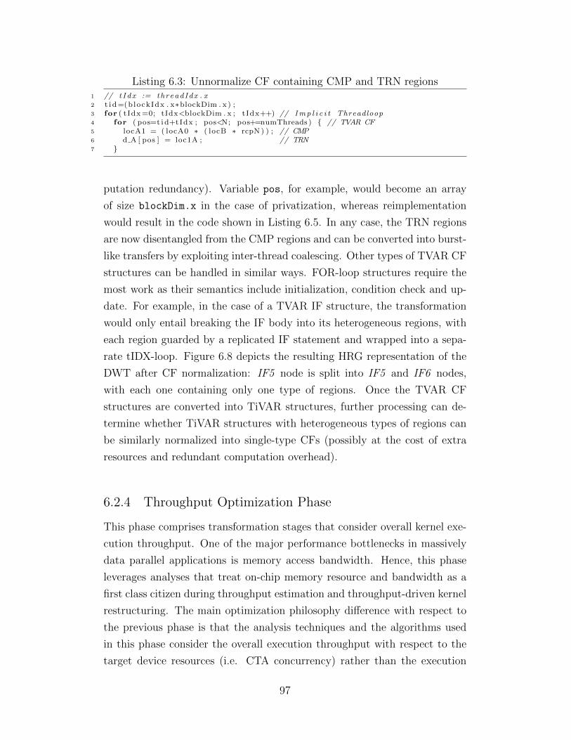
Listing 6.3: Unnormalize CF containing CMP and TRN regions1 // t I dx := threadIdx . x2 t i d=(blockIdx . x∗blockDim . x ) ;3 for ( t Idx=0; tIdx<blockDim . x ; t Idx++) // Imp l i c i t Threadloop4 for ( pos=t i d+tIdx ; pos<N; pos+=numThreads ) { // TVAR CF5 locA1 = ( locA0 ∗ ( locB ∗ rcpN ) ) ; // CMP6 d A [ pos ] = loc1A ; // TRN7 }
putation redundancy). Variable pos, for example, would become an array
of size blockDim.x in the case of privatization, whereas reimplementation
would result in the code shown in Listing 6.5. In any case, the TRN regions
are now disentangled from the CMP regions and can be converted into burst-
like transfers by exploiting inter-thread coalescing. Other types of TVAR CF
structures can be handled in similar ways. FOR-loop structures require the
most work as their semantics include initialization, condition check and up-
date. For example, in the case of a TVAR IF structure, the transformation
would only entail breaking the IF body into its heterogeneous regions, with
each region guarded by a replicated IF statement and wrapped into a sepa-
rate tIDX-loop. Figure 6.8 depicts the resulting HRG representation of the
DWT after CF normalization: IF5 node is split into IF5 and IF6 nodes,
with each one containing only one type of regions. Once the TVAR CF
structures are converted into TiVAR structures, further processing can de-
termine whether TiVAR structures with heterogeneous types of regions can
be similarly normalized into single-type CFs (possibly at the cost of extra
resources and redundant computation overhead).
6.2.4 Throughput Optimization Phase
This phase comprises transformation stages that consider overall kernel exe-
cution throughput. One of the major performance bottlenecks in massively
data parallel applications is memory access bandwidth. Hence, this phase
leverages analyses that treat on-chip memory resource and bandwidth as a
first class citizen during throughput estimation and throughput-driven kernel
restructuring. The main optimization philosophy difference with respect to
the previous phase is that the analysis techniques and the algorithms used
in this phase consider the overall execution throughput with respect to the
target device resources (i.e. CTA concurrency) rather than the execution
97
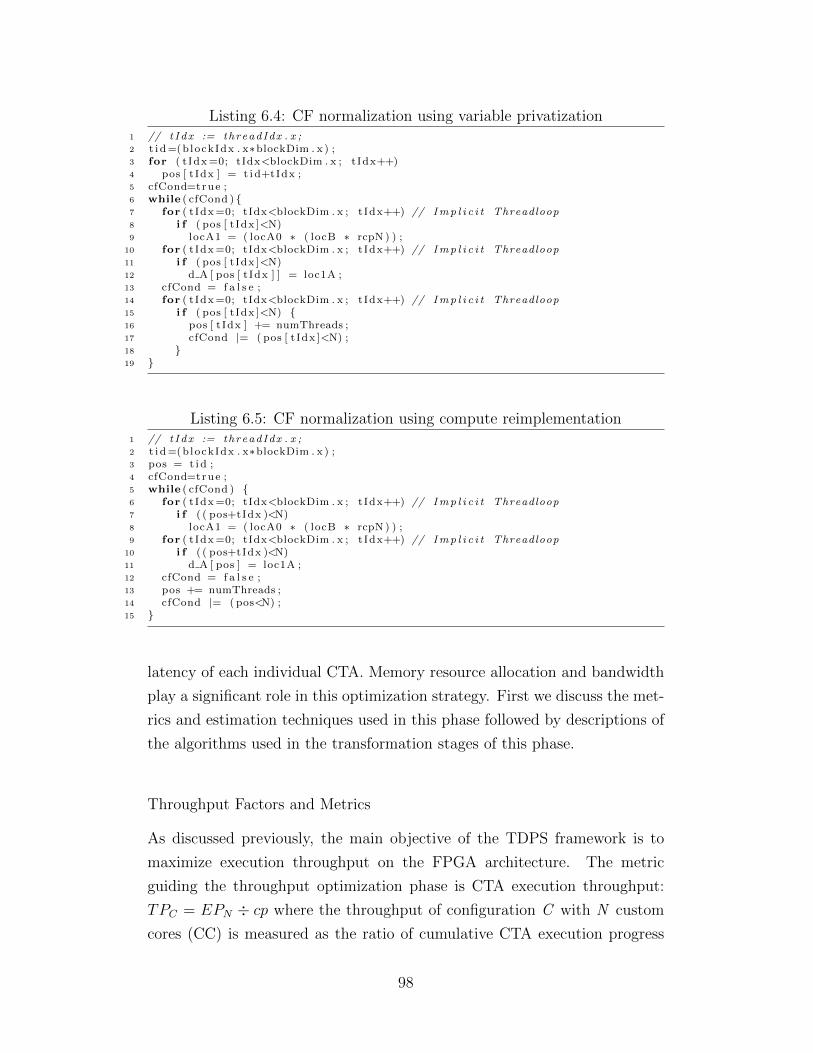
Listing 6.4: CF normalization using variable privatization1 // t I dx := threadIdx . x ;2 t i d=(blockIdx . x∗blockDim . x ) ;3 for ( t Idx=0; tIdx<blockDim . x ; t Idx++)4 pos [ t Idx ] = t i d+tIdx ;5 cfCond=true ;6 while ( cfCond ) {7 for ( t Idx=0; tIdx<blockDim . x ; t Idx++) // Imp l i c i t Threadloop8 i f ( pos [ t Idx ]<N)9 locA1 = ( locA0 ∗ ( locB ∗ rcpN ) ) ;
10 for ( t Idx=0; tIdx<blockDim . x ; t Idx++) // Imp l i c i t Threadloop11 i f ( pos [ t Idx ]<N)12 d A [ pos [ t Idx ] ] = loc1A ;13 cfCond = f a l s e ;14 for ( t Idx=0; tIdx<blockDim . x ; t Idx++) // Imp l i c i t Threadloop15 i f ( pos [ t Idx ]<N) {16 pos [ t Idx ] += numThreads ;17 cfCond |= ( pos [ t Idx ]<N) ;18 }19 }
Listing 6.5: CF normalization using compute reimplementation1 // t I dx := threadIdx . x ;2 t i d=(blockIdx . x∗blockDim . x ) ;3 pos = t i d ;4 cfCond=true ;5 while ( cfCond ) {6 for ( t Idx=0; tIdx<blockDim . x ; t Idx++) // Imp l i c i t Threadloop7 i f ( ( pos+tIdx )<N)8 locA1 = ( locA0 ∗ ( locB ∗ rcpN ) ) ;9 for ( t Idx=0; tIdx<blockDim . x ; t Idx++) // Imp l i c i t Threadloop
10 i f ( ( pos+tIdx )<N)11 d A [ pos ] = loc1A ;12 cfCond = f a l s e ;13 pos += numThreads ;14 cfCond |= ( pos<N) ;15 }
latency of each individual CTA. Memory resource allocation and bandwidth
play a significant role in this optimization strategy. First we discuss the met-
rics and estimation techniques used in this phase followed by descriptions of
the algorithms used in the transformation stages of this phase.
Throughput Factors and Metrics
As discussed previously, the main objective of the TDPS framework is to
maximize execution throughput on the FPGA architecture. The metric
guiding the throughput optimization phase is CTA execution throughput:
TPC = EPN ÷ cp where the throughput of configuration C with N custom
cores (CC) is measured as the ratio of cumulative CTA execution progress
98
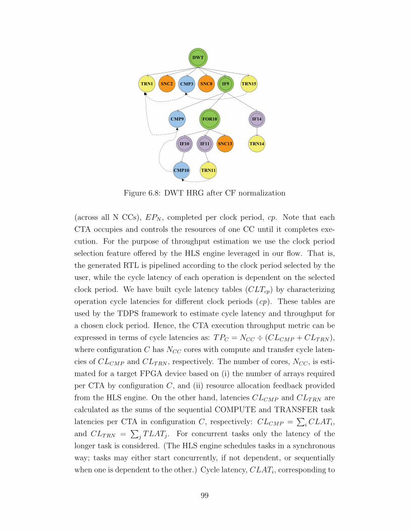
DWT
IF9TRN1 SNC2 CMP3 TRN15SNC8
CMP9
SNC13
CMP10 TRN11
TRN14
IF14
IF10
FOR10
IF11
Figure 6.8: DWT HRG after CF normalization
(across all N CCs), EPN , completed per clock period, cp. Note that each
CTA occupies and controls the resources of one CC until it completes exe-
cution. For the purpose of throughput estimation we use the clock period
selection feature offered by the HLS engine leveraged in our flow. That is,
the generated RTL is pipelined according to the clock period selected by the
user, while the cycle latency of each operation is dependent on the selected
clock period. We have built cycle latency tables (CLTcp) by characterizing
operation cycle latencies for different clock periods (cp). These tables are
used by the TDPS framework to estimate cycle latency and throughput for
a chosen clock period. Hence, the CTA execution throughput metric can be
expressed in terms of cycle latencies as: TPC = NCC ÷ (CLCMP + CLTRN),
where configuration C has NCC cores with compute and transfer cycle laten-
cies of CLCMP and CLTRN , respectively. The number of cores, NCC , is esti-
mated for a target FPGA device based on (i) the number of arrays required
per CTA by configuration C, and (ii) resource allocation feedback provided
from the HLS engine. On the other hand, latencies CLCMP and CLTRN are
calculated as the sums of the sequential COMPUTE and TRANSFER task
latencies per CTA in configuration C, respectively: CLCMP =∑
iCLATi,
and CLTRN =∑
j TLATj. For concurrent tasks only the latency of the
longer task is considered. (The HLS engine schedules tasks in a synchronous
way; tasks may either start concurrently, if not dependent, or sequentially
when one is dependent to the other.) Cycle latency, CLATi, corresponding to
99
COMPUTE task tski, is estimated by determining the task’s critical execu-
tion path. Def-Use chains are used for identifying the critical execution path,
while operation cycle latencies are referenced from CLTcp characterization
tables. TLATj, on the other hand, is the cycle latency estimate for TRANS-
FER task tskj. The TRANSFER latency is affected by two main factors:
(i) the on-chip memory bandwidth and (ii) the off-chip memory bandwidth.
The former is estimated based on the on-chip SRAM memory port band-
width (SMPBW ), the execution frequency and the read/write data volume.
The latter depends on the off-chip DDR memory system peak bandwidth
(DMBW , provided by the user), the extent of static coalescing achieved by
the burst conversion stage in the latency optimization phase (Section 6.2.3)
and the read/write data volume of the task. The final TRANSFER task la-
tency is calculated as TLATj = max(SMLATj, DMLATj), where SMLATi
corresponds to the on-chip memory access latency and DMLATi corresponds
to the off-chip memory access latency. It can be easily deduced from the pre-
vious description that SMLATj is mainly dependent on the architecture of
the examined configuration, C, while DMLATi is mainly constrained by the
value of DMBW provided by the user. The Throughput Optimization phase
aims to adjust the value of SMLATj as close as possible to the value of
DMLATj in order to take advantage of the maximum possible DDR band-
width while avoiding unnecessary over-allocation of on-chip memory resource.
Throughput-Driven Graph Coloring
Graph coloring has been traditionally used in compilers for allocation of
software-accessible registers to variables, temporary results or large constants
[79, 80]. Register allocation in CPUs is extremely important as it can af-
fect performance significantly. The volatile memory hierarchy of modern
microprocessors comprises multiple memory levels starting with registers (or
register-files) at the bottom of the memory hierarchy and ending with DRAM
memory modules at the top. Each upper level provides bigger storage capac-
ity at lower access bandwidth and higher latency. Graph coloring has been
shown to provide an efficient solution for allocating the precious, but ex-
tremely limited, register resource. In CUDA, the SIMT programming model
offers visibility of the different memory hierarchy levels, enabling the GPU
programmer to have significant control of the memory hierarchy allocation
100
to kernel data. Hence, CUDA kernels are often designed with consideration
of the memory hierarchy of the target GPU device. The throughput-driven
graph coloring (TDGC) stage of the TDPS framework aims to enhance the
allocation of the on-chip FPGA memories (BRAMs), considering both the
kernel code characteristics and the resource capacity of the target recon-
figurable device. It uses graph coloring within a novel memory allocation
algorithm that determines two main implementation issues: (i) allocation of
arrays onto BRAMs and (ii) scheduling of data communication between off-
chip and on-chip memory levels. Note that in the S2C flow, individual thread
data transfers to/from off-chip DDR memory are organized in TRANSFER
tasks per CTA in order to take advantage of the DDR memory burst ca-
pability and coalesced data access patterns in the kernel. The TDGC stage
entails three main steps: (GC1 ) BRAM allocation to array variables through
array lifetime coloring, (GC2 ) Execution throughput evaluation, and (GC3 )
TRANSFER task rescheduling. The three steps may be iterated until no
other potentially promising region motions are available. In most cases, the
number of iterations is small.
Each array variable in the kernel code is mapped to a separate BRAM by
the HLS tool. Thus, different array variables with non-overlapping lifetimes
will be allocated to different BRAMs. This may lead to precious BRAM
resource waste and reduced throughput, as a result. Hence, through graph
coloring the TDGC stage aims to optimize sharing of BRAMs between arrays
and find optimal TRANSFER task invocation points, in terms of throughput.
Initially, the candidate arrays for allocation are identified (step GC1 ) and
their lifetime, aLT , is computed and defined as a set of live-intervals. Live-
intervals are represented by sID (statement ID) pairs, aLT = {[sIDi, sIDj}.A lifetime, aLT , may comprise multiple live-intervals in case it can be deter-
mined that the corresponding array is only live across a subset of divergent
control flows with partially ordered sID ranges. Subsequently, an interfer-
ence graph, GI = (V,E), is generated based on the lifetime relations of the
arrays. The nodes, V , of GI correspond to the lifetime instances (i.e. an
array variable, Va may correspond to more than one lifetime instances, if, for
example, all of its elements are killed by an intermediate definition between
two different uses). An edge in set E of graph GI connects two lifetime nodes
if the beginning sID of one of them lies within one of the live-interval of the
other one (this way of interference edge generation results in fewer edges
101
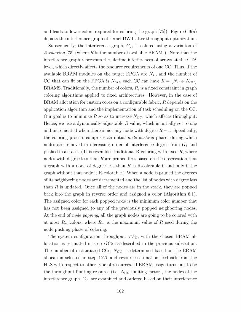
and leads to fewer colors required for coloring the graph [75]). Figure 6.9(a)
depicts the interference graph of kernel DWT after throughput optimization.
Subsequently, the interference graph, GI , is colored using a variation of
R-coloring [75] (where R is the number of available BRAMs). Note that the
interference graph represents the lifetime interferences of arrays at the CTA
level, which directly affects the resource requirements of one CC. Thus, if the
available BRAM modules on the target FPGA are NB, and the number of
CC that can fit on the FPGA is NCC , each CC can have R = bNB ÷ NCCcBRAMS. Traditionally, the number of colors, R, is a fixed constraint in graph
coloring algorithms applied to fixed architectures. However, in the case of
BRAM allocation for custom cores on a configurable fabric, R depends on the
application algorithm and the implementation of task scheduling on the CC.
Our goal is to minimize R so as to increase NCC , which affects throughput.
Hence, we use a dynamically adjustable R value, which is initially set to one
and incremented when there is not any node with degree R− 1. Specifically,
the coloring process comprises an initial node pushing phase, during which
nodes are removed in increasing order of interference degree from GI and
pushed in a stack. (This resembles traditional R-coloring with fixed R, where
nodes with degree less than R are pruned first based on the observation that
a graph with a node of degree less than R is R-colorable if and only if the
graph without that node is R-colorable.) When a node is pruned the degrees
of its neighboring nodes are decremented and the list of nodes with degree less
than R is updated. Once all of the nodes are in the stack, they are popped
back into the graph in reverse order and assigned a color (Algorithm 6.1).
The assigned color for each popped node is the minimum color number that
has not been assigned to any of the previously popped neighboring nodes.
At the end of node popping, all the graph nodes are going to be colored with
at most Rm colors, where Rm is the maximum value of R used during the
node pushing phase of coloring.
The system configuration throughput, TPC , with the chosen BRAM al-
location is estimated in step GC2 as described in the previous subsection.
The number of instantiated CCs, NCC , is determined based on the BRAM
allocation selected in step GC1 and resource estimation feedback from the
HLS with respect to other type of resources. If BRAM usage turns out to be
the throughput limiting resource (i.e. NCC limiting factor), the nodes of the
interference graph, GI , are examined and ordered based on their interference
102
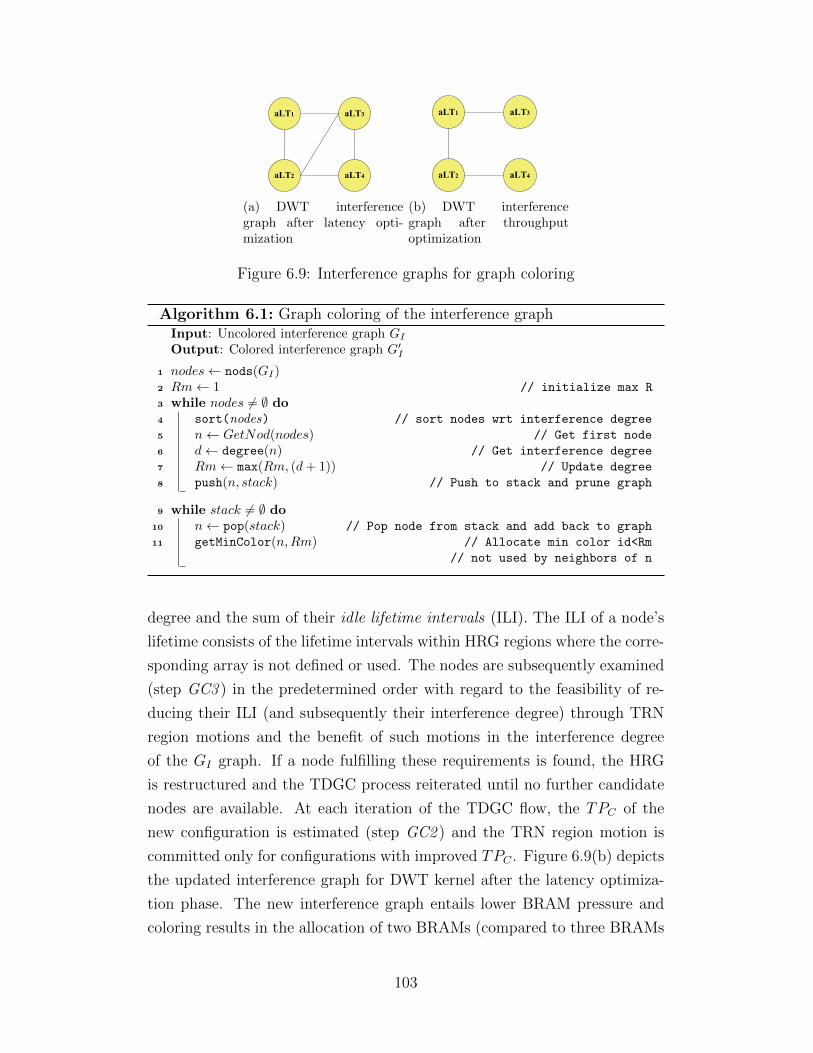
aLT1 aLT3
aLT2 aLT4
(a) DWT interferencegraph after latency opti-mization
aLT1 aLT3
aLT2 aLT4
(b) DWT interferencegraph after throughputoptimization
Figure 6.9: Interference graphs for graph coloring
Algorithm 6.1: Graph coloring of the interference graphInput: Uncolored interference graph GI
Output: Colored interference graph G′I
1 nodes← nods(GI)2 Rm← 1 // initialize max R
3 while nodes 6= ∅ do4 sort(nodes) // sort nodes wrt interference degree
5 n← GetNod(nodes) // Get first node
6 d← degree(n) // Get interference degree
7 Rm← max(Rm, (d + 1)) // Update degree
8 push(n, stack) // Push to stack and prune graph
9 while stack 6= ∅ do10 n← pop(stack) // Pop node from stack and add back to graph
11 getMinColor(n,Rm) // Allocate min color id<Rm
// not used by neighbors of n
degree and the sum of their idle lifetime intervals (ILI). The ILI of a node’s
lifetime consists of the lifetime intervals within HRG regions where the corre-
sponding array is not defined or used. The nodes are subsequently examined
(step GC3 ) in the predetermined order with regard to the feasibility of re-
ducing their ILI (and subsequently their interference degree) through TRN
region motions and the benefit of such motions in the interference degree
of the GI graph. If a node fulfilling these requirements is found, the HRG
is restructured and the TDGC process reiterated until no further candidate
nodes are available. At each iteration of the TDGC flow, the TPC of the
new configuration is estimated (step GC2 ) and the TRN region motion is
committed only for configurations with improved TPC . Figure 6.9(b) depicts
the updated interference graph for DWT kernel after the latency optimiza-
tion phase. The new interference graph entails lower BRAM pressure and
coloring results in the allocation of two BRAMs (compared to three BRAMs
103
for the initial interference graph in Figure 6.9(a)).
6.3 Evaluation
The TDPS framework is implemented within the FCUDA flow (Chapter
4) and the analysis phase (Figure 6.1) replaces, essentially, the (manual)
annotation stage shown in Figure 4.1. Moreover, the latency and throughput
optimization phases of TDPS are integrated at the frontend of the FCUDA-
compilation stage (Figure 4.1) to apply throughput-driven code restructuring
prior to compiling the SIMT code into implicitly parallel C code for the HLS
engine. The HLS engine integrated in the flow is Vivado-HLS [81], which is
the successor of AutoPilot HLS engine [31] used in FCUDA (Chapter 4).
The philosophy of the TDPS evaluation in this section is centered around
exposing the performance effects of the transformations applied by TDPS.
Specifically, in the next section we measure the performance impact of the
latency optimization transformation stages to the kernel compute latency.
Subsequently, the effectiveness of the metric used to guide throughput op-
timization is evaluated in Section 6.3.2. Finally, we compare the total ker-
nel execution latency achieved by the TDPS-enhanced flow vs. the original
FCUDA flow in Section 6.3.3. The CUDA kernel benchmarks used in all of
the evaluations are described in Table 4.2. The original floating-point ker-
nels, as well as derived integer kernel versions, are used to further explore
the effectivenes of TDPS optimizations across compute systems with different
precision and range capabilities as well as resource and latency overheads.
Moreover, we also explore the adaptiveness of TDPS to different target FPGA
architectures by measuring the execution latency on two different families of
Virtex FPGAs. Finally, for some benchmarks we examine the effect of TDPS
optimization in relation to code optimizations enabled by different Vivado-
HLS performance-boosting directives. In particular, for the MM kernel which
contains compute intensive loops we apply the loop pipelining directive and
treat the optimized code (MMp) as a separate kernel version.
104
6.3.1 Latency Optimization Phase Evaluation
First we evaluate the performance effect of the different optimizations and
transformations applied during the latency optimization phase (Figure 6.1)
on the CTA compute latency. In other words, we evaluate the speedup of
each CC, considering only the COMPUTE tasks of each kernel. Figure 6.10
depicts the compute speedup achieved over FCUDA compilation by applying
growing subsets of the TDPS optimizations; i.e., speedup from TRN motions
(TM) entails SNC motions (SM) and branch conversion (BC). The speedup
achieved by each latency optimization depends on the kernel code character-
istics. Kernels that either contain long dataflow paths (e.g. FWT2) or more
convoluted control flow paths (e.g DWT) offer more opportunity for optimiza-
tion. We can see that TRN motions (TM) can have significant impact in the
compute latency (e.g. FWT2 and DWT). This is due to enabling the genera-
tion of coarser COMPUTE tasks, by shifting TRN regions out of the way. It
is interesting to observe that burst conversion (BC) results in good speedups
for some kernels (e.g. FWT1 and FWT2), even though TRANSFER task
latency is not included in this evaluation. The main reason for this is due
to the address calculation simplification from consolidating the memory ad-
dress computation from all the threads into burst address computations at
the CTA level. On the other hand, SNC region motions do not seem to affect
compute latency in a considerable way. However, they enable elimination of
excessive variable privatization during FCUDA backend compilation phase,
which benefits BRAM resource requirements and hence throughput. Finally,
we would like to point out that the bars corresponding to the MMp kernel
in Figure 6.10 are normalized with respect to the FCUDA bar of MM ker-
nel. This comparison shows that despite the significant speedup achieved by
loop pipelining enabled by the HLS directive engine, TDPS achieves further
speedup improvement.
6.3.2 Throughput Optimization Phase Evaluation
In this section we measure the correlation between the throughput estima-
tion metric and the actual execution latency. For this purpose we use the
DWT kernel that has served as a running example throughout the previous
sections. Specifically, intermediate configurations Ci, of DWT kernel during
105
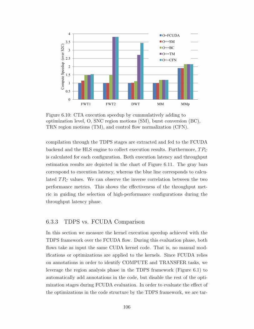
1.5
2
2.5
3
3.5
4
e Sp
eedu
p (o
ver S
2C)
O=FCUDA
O+=SM
O+=BC
O+=TM
O+=CFN
0
0.5
1
.5
FWT1 FWT2 DWT MM MMp
Com
pute
Figure 6.10: CTA execution speedup by cummulatively adding tooptimization level, O, SNC region motions (SM), burst conversion (BC),TRN region motions (TM), and control flow normalization (CFN).
compilation through the TDPS stages are extracted and fed to the FCUDA
backend and the HLS engine to collect execution results. Furthermore, TPC
is calculated for each configuration. Both execution latency and throughput
estimation results are depicted in the chart of Figure 6.11. The gray bars
correspond to execution latency, whereas the blue line corresponds to calcu-
lated TPC values. We can observe the inverse correlation between the two
performance metrics. This shows the effectiveness of the throughput met-
ric in guiding the selection of high-performance configurations during the
throughput latency phase.
6.3.3 TDPS vs. FCUDA Comparison
In this section we measure the kernel execution speedup achieved with the
TDPS framework over the FCUDA flow. During this evaluation phase, both
flows take as input the same CUDA kernel code. That is, no manual mod-
ifications or optimizations are applied to the kernels. Since FCUDA relies
on annotations in order to identify COMPUTE and TRANSFER tasks, we
leverage the region analysis phase in the TDPS framework (Figure 6.1) to
automatically add annotations in the code, but disable the rest of the opti-
mization stages during FCUDA evaluation. In order to evaluate the effect of
the optimizations in the code structure by the TDPS framework, we are tar-
106
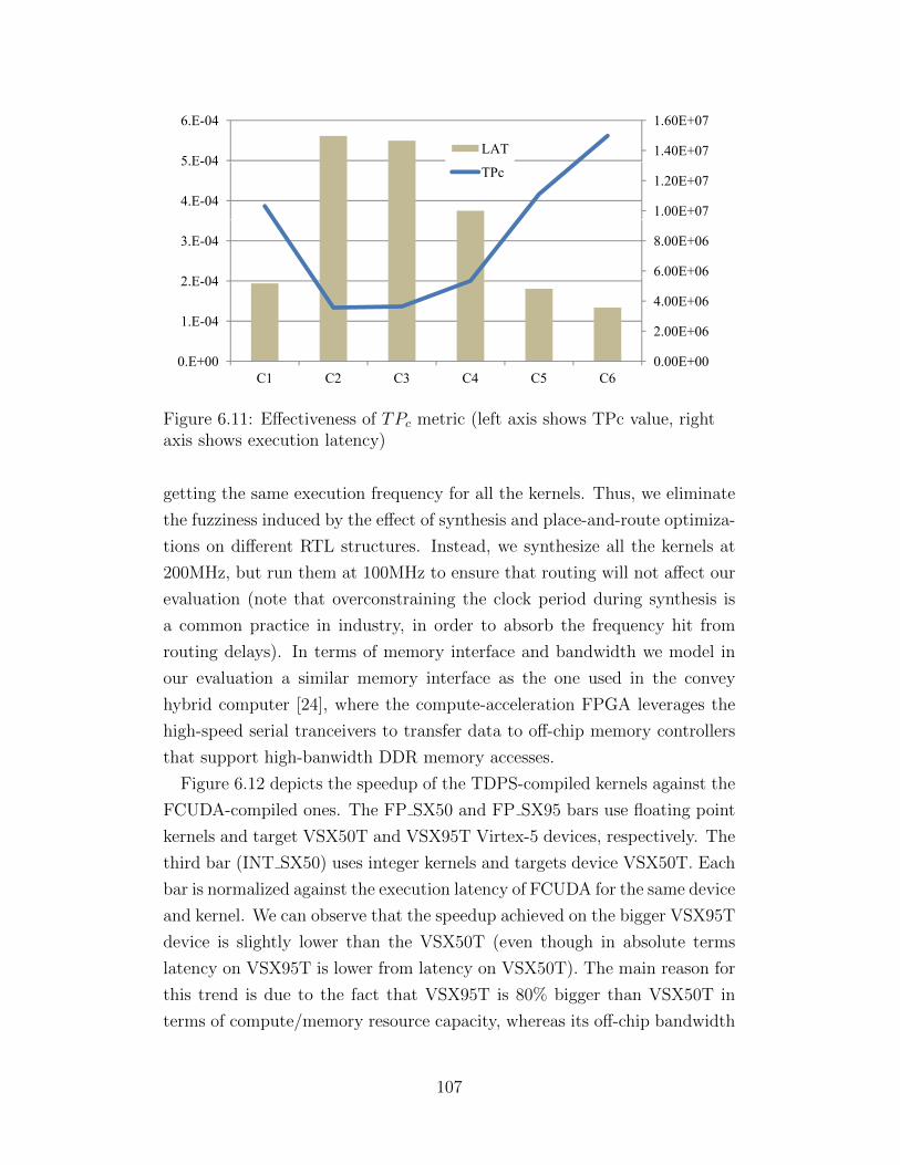
1.40E+07
1.60E+07
5 E-04
6.E-04
LAT
1.00E+07
1.20E+074.E-04
5.E-04TPc
6.00E+06
8.00E+06
2 E 04
3.E-04
2.00E+06
4.00E+061.E-04
2.E-04
0.00E+00
2.00E 06
0.E+00C1 C2 C3 C4 C5 C6
Figure 6.11: Effectiveness of TPc metric (left axis shows TPc value, rightaxis shows execution latency)
getting the same execution frequency for all the kernels. Thus, we eliminate
the fuzziness induced by the effect of synthesis and place-and-route optimiza-
tions on different RTL structures. Instead, we synthesize all the kernels at
200MHz, but run them at 100MHz to ensure that routing will not affect our
evaluation (note that overconstraining the clock period during synthesis is
a common practice in industry, in order to absorb the frequency hit from
routing delays). In terms of memory interface and bandwidth we model in
our evaluation a similar memory interface as the one used in the convey
hybrid computer [24], where the compute-acceleration FPGA leverages the
high-speed serial tranceivers to transfer data to off-chip memory controllers
that support high-banwidth DDR memory accesses.
Figure 6.12 depicts the speedup of the TDPS-compiled kernels against the
FCUDA-compiled ones. The FP SX50 and FP SX95 bars use floating point
kernels and target VSX50T and VSX95T Virtex-5 devices, respectively. The
third bar (INT SX50) uses integer kernels and targets device VSX50T. Each
bar is normalized against the execution latency of FCUDA for the same device
and kernel. We can observe that the speedup achieved on the bigger VSX95T
device is slightly lower than the VSX50T (even though in absolute terms
latency on VSX95T is lower from latency on VSX50T). The main reason for
this trend is due to the fact that VSX95T is 80% bigger than VSX50T in
terms of compute/memory resource capacity, whereas its off-chip bandwidth
107
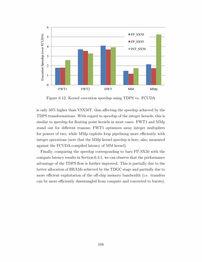
5
6
DA
) FP_SX50
4
5ve
r FC
UD
FP_SX95
INT_SX50
3
peed
up (o
v
1
2
xecu
tion
Sp
0FWT1 FWT2 DWT MM MMp
Ex
Figure 6.12: Kernel execution speedup using TDPS vs. FCUDA
is only 50% higher than VSX50T, thus affecting the speedup achieved by the
TDPS transformations. With regard to speedup of the integer kernels, this is
similar to speedup for floating point kernels in most cases. FWT1 and MMp
stand out for different reasons; FWT1 optimizes away integer multipliers
for powers of two, while MMp exploits loop pipelining more efficiently with
integer operations (note that the MMp kernel speedup is here, also, measured
against the FCUDA-compiled latency of MM kernel).
Finally, comparing the speedup corresponding to bars FP SX50 with the
compute latency results in Section 6.3.1, we can observe that the performance
advantage of the TDPS flow is further improved. This is partially due to the
better allocation of BRAMs achieved by the TDGC stage and partially due to
more efficient exploitation of the off-chip memory bandwidth (i.e. transfers
can be more efficiently disentangled from compute and converted to bursts).
108
CHAPTER 7
CONCLUSION
The power wall faced by traditional ILP-driven CPUs during the last decade
has caused a major shift towards parallel computing in every compute seg-
ment. This shift has been further enabled and encouraged by two other
factors: (i) the continuing increase of on-chip compute and storage capac-
ity due to the transistor feature shrinking size and (ii) the emergence of
compute intensive applications with high degree of inherent parallelism (e.g.
high-definition processing, fluid dynamics and N-body simulation). Never-
theless the need to achieve high throughput in these massively parallel appli-
cations, without losing the ILP-oriented performance features of traditional
CPUs, is pushing toward a heterogeneous compute ecosystem. A common
heterogeneous configuration today is available on almost every new PC moth-
erboard which includes a general purpose compute capable GPU. Moreover,
the power and performance advantages of FPGA (and ASIC) custom proces-
sors are the reason that several vendors offer cards that host CPUs together
with FPGAs. However, in order to exploit the benefits of reconfigurable de-
vices in a wide range of applications, it is important to achieve both efficient
programmability and high performance. That is, having high performance
at the cost of programmability or vice versa is not going to be acceptable by
the high-performance community.
In this dissertation, we first propose a high-level synthesis flow for enhanced
parallelism extraction from C applications onto a custom processor, named
EPOS. EPOS is a stylized microcode-driven processor with an architecture
that is customized to exploit instruction level parallelism beyond the basic
block boundary. In particular, the EPOS synthesis flow is based on advanced
compiler techniques for high ILP identification which is subsequently mapped
onto the customized EPOS architecture.
As the use of reconfigurable and ASIC custom processors in heterogeneous
systems is going to be better suited for the acceleration of massively paral-
109
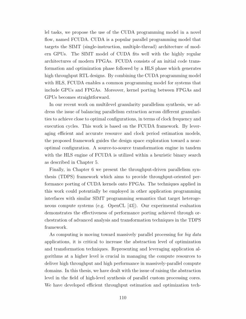
lel tasks, we propose the use of the CUDA programming model in a novel
flow, named FCUDA. CUDA is a popular parallel programming model that
targets the SIMT (single-instruction, multiple-thread) architecture of mod-
ern GPUs. The SIMT model of CUDA fits well with the highly regular
architectures of modern FPGAs. FCUDA consists of an initial code trans-
formation and optimization phase followed by a HLS phase which generates
high throughput RTL designs. By combining the CUDA programming model
with HLS, FCUDA enables a common programming model for systems that
include GPUs and FPGAs. Moreover, kernel porting between FPGAs and
GPUs becomes straightforward.
In our recent work on multilevel granularity parallelism synthesis, we ad-
dress the issue of balancing parallelism extraction across different granulari-
ties to achieve close to optimal configurations, in terms of clock frequency and
execution cycles. This work is based on the FCUDA framework. By lever-
aging efficient and accurate resource and clock period estimation models,
the proposed framework guides the design space exploration toward a near-
optimal configuration. A source-to-source transformation engine in tandem
with the HLS engine of FCUDA is utilized within a heuristic binary search
as described in Chapter 5.
Finally, in Chapter 6 we present the throughput-driven parallelism syn-
thesis (TDPS) framework which aims to provide throughput-oriented per-
formance porting of CUDA kernels onto FPGAs. The techniques applied in
this work could potentially be employed in other application programming
interfaces with similar SIMT programming semantics that target heteroge-
neous compute systems (e.g. OpenCL [43]). Our experimental evaluation
demonstrates the effectiveness of performance porting achieved through or-
chestration of advanced analysis and transformation techniques in the TDPS
framework.
As computing is moving toward massively parallel processing for big data
applications, it is critical to increase the abstraction level of optimization
and transformation techniques. Representing and leveraging application al-
gorithms at a higher level is crucial in managing the compute resources to
deliver high throughput and high performance in massively-parallel compute
domains. In this thesis, we have dealt with the issue of raising the abstraction
level in the field of high-level synthesis of parallel custom processing cores.
We have developed efficient throughput estimation and optimization tech-
110

niques that improve performance beyond the thread-latency level by dealing
with conflicting performance factors at the thread-group level and managing
the compute and storage resources accordingly.
111
REFERENCES
[1] “The Cell project at IBM Research,” IBM. [Online]. Available:http://www.research.ibm.com/cell/
[2] “Manycore without boundaries,” TILERA. [Online]. Available:http://www.tilera.com/producs/processors
[3] “ATI Radeon HD 5000 Series,” 2011, AMD. [Online]. Avail-able: http://www.amd.com/us/products/desktop/graphics/ati-radeon-hd-5000/Pages/ati-radeon-hd-5000.aspx
[4] “High performance computing - supercomputing withTesla GPUs,” 2011, NVIDIA. [Online]. Available:http://www.nvidia.com/object/tesla computing solutions.html
[5] J. Gray, “The roadrunner supercomputer: a petaflop’s no problem,”Linux Journal, vol. 2008, no. 175, Nov. 2008.
[6] “AMD Opteron processor solutions,” 2011, AMD. [Online]. Available:http://products.amd.com/en-us/OpteronCPUResult.aspx
[7] A. D. George, H. Lam, A. Lawande, and C. Pas-coe, “Novo-G : Adaptively custom reconfigurable super-computer,” Dec. 2009, Presentation. [Online]. Available:http://www.gstitt.ece.ufl.edu/courses/fall09/eel4930 5934/lectures/Novo-G.ppt
[8] “Intel XEON processor 5500 series servers,” Intel. [Online]. Available:http://www.intel.com/itcenter/products/xeon/5500/index.htm
[9] “Stratix III device handbook, volume 1, version2.2,” Mar. 2011, Manual, ALTERA. [Online]. Available:http://www.altera.com/literature/hb/stx3/stratix3 handbook.pdf
[10] H. Meuer, E. Strohmaier, H. Simon, and J. Dongarra, “Oak ridge claimsno. 1 position on latest top500 list with titan,” Nov. 2012, Top 500.[Online]. Available: http://www.top500.org/blog/lists/2012/11/press-release/
112
[11] H. Meuer, E. Strohmaier, H. Simon, and J. Dongarra, “Chinagrabs supercomputing leadership spot in latest ranking of world’stop 500 supercomputers,” Nov. 2010, Top 500. [Online]. Available:http://www.top500.org/lists/2010/11/press-release
[12] “Virtex II Pro and Virtex II Pro X Plat-form FPGAs: complete datasheet, version 4.7,”Nov. 2007, Datasheet, XILINX. [Online]. Available:http://www.xilinx.com/support/documentation/data sheets/ds083.pdf
[13] R. Wilson, “CPUs in FPGAs: many faces to a trend,” EDN,Mar. 2011. [Online]. Available: http://www.edn.com/article/517118-CPUs in FPGAs many faces to a trend.php
[14] “Intel Core i7-600, i5-500, i5-400 and i3-300 mobile processorseries,” Datasheet, Volume one, Intel, Jan. 2010. [Online]. Available:http://download.intel.com/design/processor/datashts/322812.pdf
[15] “AMD Fusion family of APUs: Enabling a superior, immersive PCexperience,” White Paper, AMD, Mar. 2010. [Online]. Available:http://sites.amd.com/us/Documents/48423B fusion whitepaper WEB.pdf
[16] R. Merritt, “Intel packs Atom into tablets, set-tops, FPGAs,” EE Times,Sep. 2010. [Online]. Available: http://www.eetimes.com/electronics-news/4207694/Intel-packs-Atom-into-tablets–set-tops–FPGAs
[17] M. Showerman, J. Enos, C. Kidratenko, C. Steffer, R. Pennington,and W. W. Hwu, “QP: A Heterogeneous Multi-Accelerator Cluster,” inProc. 10th LCI International Conference on High-Performance CLus-tered Computing, Boulder, Colorado, Mar. 2009.
[18] K. H. Tsoi and W. Luk, “Axel: A Heterogeneous Cluster with FP-GAs and GPUs,” in Proc. ACM/SIDGA International Symposium onField Programmable Gate Arrays (FPGA’10), Monterey, California, Feb.2010.
[19] G. Gilat, “Automated FPGA to ASIC conversion withzero NRE,” White Paper, KaiSemi, Feb. 2011. [Online].Available: http://www.eetimes.com/electrical-engineers/education-training/tech-papers/4213116/Automated-FPGA-to-ASIC-Conversion
[20] S. Che, J. Li, J. W. Sheaffer, K. Skadron, and J. Lach, “Acceleratingcompute-intensive applications with GPUs and FPGAs,” in Proc. IEEESymposium on Application Specific Processors (SASP’08), June 2008.
[21] J. Cong and Y. Zou, “Lithographic aerial image simulation with FPGA-based hardware acceleration,” in Proc. ACM/SIGDA InternationalSymposium on Field Programmable Gate Arrays (FPGA’08), Feb. 2008.
113
[22] J. Cho, S. Mirzaei, J. Oberg, and R. Kastner, “FPGA-based face detec-tion system using haar classifiers,” in Proc. ACM/SIGDA InternationalSymposium on Field Programmable Gate Arrays (FPGA’09), Feb. 2009.
[23] C. He, A. Papakonstantinou, and D. Chen, “A novel SoC architectureon FPGA for ultra fast face detection,” in Proc. IEEE InternationalConference on Computer Design (ICCD’09), Oct. 2009.
[24] “The Convey HC-1: The world’s first hybrid corecomputer,” 2009, Datasheet, Convey Computer. [On-line]. Available: http://www.conveycomputer.com/Resources/HC-1%20Data%20Sheet.pdf
[25] J. Williams, J. Richardson, K. Gosrani, and S. Suresh, “Computationaldensity of fixed and reconfigurable multi-core devices for applicationacceleration,” in Proc. Reconfigurable Systems Summer Institute 2008(RSSI), Urbana, Illinois, July 2008.
[26] Oak Ridge National Laboratory, “Oak Ridge ’Jaguar’ supercomputeris world’s fastest,” Science Daily, Nov. 2009. [Online]. Available:http://www.sciencedaily.com/releases/2009/11/091116204229.htm
[27] P. Coussy, D. Gajski, M. Meredith, and A. Takach, “An introduction tohigh-level synthesis,” IEEE Design & Test of Computers, vol. 26, no. 4,pp. 8–17, July 2009.
[28] J. W. Sias, S. Ueng, G. Kent, I. Steiner, E. Nystrom, and W. W. Hwu,“Field-testing IMPACT EPIC research results in Itanium 2,” in Proc.31st International Symposium on Computer Architecture (ISCA’04),July 2004, pp. 26–37.
[29] “Impulse Codeveloper,” 2010, Impulse Accelerated Technologies.[Online]. Available: http://www.impulsec.com
[30] “Catapult C synthesis,” 2010, Mentor Graphics. [Online]. Available:http://www.mentor.com/products/esl/high level synthesis/catapult synthesis/
[31] Z. Y. Zhang, F. W. Jiang, G. Han, C. Yang, and J. Cong, “Autopilot: Aplatform-based ESL synthesis system,” in High-Level Synthesis: FromAlgorithm to Digital Circuit, P. Coussy and A. Moraviec, Eds. Springer,2008, ch. 6, pp. 99–112.
[32] J. Cong, Y. Fan, G. Han, W. Jiang, and Z. Zhang, “Platform-basedbehavior-level and system-level synthesis,” in Proc. IEEE InternationalSOC Conference, Sep. 2006, pp. 192–202.
114
[33] P. Diniz, M. Hall, J. Park, B. So, and H. Ziegler, “Automatic mappingof C to FPGAs with the DEFACTO compilation and synthesis system,”Microprocessors and Microsystems, vol. 29, no. 2-3, pp. 51–62, Apr.2005.
[34] M. Reshadi, B. Gorjiara, and D. Gajski, “Utilizing horizontal and ver-tical parallelism with a no-instruction-set compiler for custom datap-aths,” in Proc. IEEE International Conference on Computer Design(ICCD’05), Oct. 2005.
[35] H. Ziegler and M. Hall, “Evaluating heuristics in automatically map-ping multi-loop applications to FPGAs,” in Proc. ACM InternationalSymposium on Field Programmable Gate Arrays (FPGA’05), Feb. 2005.
[36] B. So, P. C. Diniz, and M. W. Hall, “Using estimates from behavioralsynthesis tools in compiler-directed design space exploration,” in Proc.IEEE/ACM Design Automation Conference (DAC’03), June 2003.
[37] J. Cong, Y. Fan, and W. Jiang, “Platform-based resource binding usinga distributed register-file microarchitecture,” in Proc. ACM/IEEE In-ternational Conference on Computer Aided Design (ICCAD’06), Nov.2006, pp. 709–715.
[38] K. H. Lim, Y. Kim, and T. Kim, “Interconnect and communica-tion synthesis for distributed register-file microarchitecture,” in Proc.IEEE/ACM Design Automation Conference (DAC’07), June 2007.
[39] J. Babb, M. Rinard, C. A. Moritz, W. Lee, M. Frank, R. Barua, andS. Amarasinghe, “Parallelizing applications into silicon,” in Proc. IEEESymposium on Field-Programmable Computing Machines (FCCM’99),1999.
[40] S. Gupta, R. Gupta, and N. Dutt, “Coordinated parallelizing compileroptimizations and high-level synthesis,” ACM Transactions on DesignAutomation of Electronic Systems, vol. 9, no. 4, pp. 441–470, 2004.
[41] S. Gupta, N. Savoiu, N. Dutt, R. Gupta, and A. Nicolau, “Using globalcode motions to improve the quality of results for high-level synthesis,”IEEE Transactions on CAD of Integrated Circuits and Systems, vol. 23,no. 2, pp. 302–312, 2004.
[42] “CUDA Zone,” 2011, NVIDIA. [Online]. Available:http://www.nvidia.com/object/cuda home new.html
[43] The OpenCL Specification, Khronos OpenCL Work-ing Group Std. 1.1, Sep. 2010. [Online]. Available:http://www.khronos.org/registry/cl/specs/opencl-1.1.pdf
115
[44] “OpenMP application program interface,” May 2008, Version3, OpenMP. [Online]. Available: http://www.openmp.org/mp-documents/spec30.pdf
[45] D. Cabrera, X. Martorell, G. Gaydadjiev, E. Ayguade, and D. Jimenez-Gonzalez, “Openmp extensions for fpga accelerators,” in Proc. IEEEInternational Symposium on Systems, Architectures, Modeling, and Sim-ulation (SAMOS’09), July 2009, pp. 17–24.
[46] Y. Leow, C. Ng, and W. Wong, “Generating hardware from OpenMPprograms,” in Proc. IEEE International Conference on Field Pro-grammable Technology (FPT’06), Dec. 2006, pp. 73–80.
[47] A. Hagiescu, W.-F. Wong, D. Bacon, and R. Rabbah, “A computingorigami: Folding streams in fpgas,” in Proc. ACM/IEEE Design Au-tomation Conference (DAC’09), July 2009, pp. 282–287.
[48] M. Owaida, N. Bellas, K. Daloukas, and C. Antonopoulos, “Synthesisof platform architectures from opencl programs,” in Proc. IEEE Sympo-sium on Field-Programmable Custom Computing Researcj (FCCM’11),May 2011.
[49] M. M. Baskaran, J. Ramanujam, and P. Sadayappan, “Automatic C-to-CUDA code generation for affine programs,” in Proc. IEEE Interna-tional Conference on Compiler Construction (CC’10), Mar. 2010.
[50] S. Lee and R. Eigenmann, “OpenMPC: Extended OpenMP program-ming and tuning for GPUs,” in Proc. ACM/IEEE Conference on Su-percomputing (SC’10), Nov. 2010.
[51] A. E. Eichenberger, K. O’Brien, K. O’Brien, P. Wu, T. Chen, P. H.Oden, D. A. Prener, J. C. Shepherd, B. So, Z. Sura, A. Wang, T. Zhang,P. Zhao, and M. Gschwind, “Optimizing compiler for a CELL proces-sor,” in Proc. IEEE International Conference on Parallel Architecturesand Compilation Techniques (PACT’10), Sep. 2005.
[52] W. W. Hwu, S. A. Mahle, W. Y. Chen, P. P. Chang, N. J. Warter, R. A.Bringmann, R. G. Ouellette, R. E. Hank, T. Kiyohara, and G. E. H.et al., “The superblock: An effective technique for VLIW and super-scalar compilation,” The Journal of Supercomputing, vol. 7, no. 1-2, pp.229–248, 1993.
[53] S. A. Mahle, D. C. Lin, W. Y. Chen, R. R. Hank, R. A. Bringmann,and W. W. Hwu, “Effective compiler support for predicated executionusing the hyperblock,” in Proc. IEEE 25th International Symposium onMicroarchitecture (MICRO 25), Dec. 1992, pp. 45–54.
116
[54] P. Chang, N. Warter, S. Mahlke, W. Chen, and W. Hwu, “Three ar-chitectural models for compiler-controlled speculative execution,” IEEETransactions on Computers, vol. 44, no. 4, pp. 481–494, 1995.
[55] K. Yeager, “The MIPS R10000 superscalar microprocessor,” IEEE Mi-cro, vol. 16, no. 2, pp. 28–40, 1996.
[56] H. Sharangpani and K. Arora, “Itanium processor microarchitecture,”IEEE Micro, vol. 20, no. 5, pp. 24–43, 2000.
[57] C. McNairy and D. Soltis, “Itanium 2 processor microarchitecture,”IEEE Micro, vol. 23, no. 2, pp. 44–55, 2003.
[58] M. Schlansker and B. Rau, “EPIC: Explicitly parallel instruction com-puting,” IEEE Computer, vol. 33, no. 2, pp. 37–45, 2000.
[59] G. Micheli, Synthesis and Optimization of Digital Circuit. McGrawHill, 1994.
[60] A. Papakonstantinou, D. Chen, and W. Hwu, “Application accelerationwith the explicitly parallel operations system - the epos processor,” inProc. IEEE Symposium on Application Specific Processors (SASP’08),June 2008.
[61] D. Chen, J. Cong, and J. Xu, “Optimal simultaneous module and multi-voltage assignment for low power,” ACM Transactions on Design Au-tomation of Electronic Systems, vol. 11, no. 2, pp. 361–386, 2006.
[62] R. Ahuja, J. Orlin, G. Sechi, and P. Zuddas, “Algorithms for the simpleequal flow problem,” Management Science, vol. 45, no. 10, pp. 1440–1455, 1999.
[63] D. Chen, J. Cong, Y. Fan, and J. Xu, “Optimality study of resourcebinding with multi-vdds,” in Proc. ACM/IEEE Design AutomationConference (DAC’06), June 2006.
[64] A. Ali, J. Kennington, and B. Shetty, “The equal flow problem,” Euro-pean Journal of Operational Research, vol. 36, pp. 107–115, 1988.
[65] “The LLVM compiler infrastructure project,” 2011. [Online]. Available:http://llvm.org/
[66] C. Dave, H. Bae, S. J. Min, S. Lee, R. Eigenmann, and S. Midkiff, “Ce-tus: A source-to-source compiler infrastructure for multicores,” IEEEComputer, vol. 42, no. 12, pp. 36–42, Dec. 2009.
[67] A. Aho, M. Lam, R. Sethi, and J. Ullman, Compilers, principles, tech-niques and tools, 2nd ed. Addison-Wesley, 2006.
117
[68] J. Stratton, S. Stone, and W. Hwu, “MCUDA: An efficient implementa-tion of CUDA kernels for multi-core cpus,” Lecture Notes in ComputerScience, vol. 5335, pp. 16–30, 2008.
[69] “Parboil benchmark suite,” 2010, IMPACT Research group, Uni-versity of ILlinois at Urbana Champaign. [Online]. Available:http://impact.crhc.illinois.edu/parboil.php
[70] J. Cong, W. Jiang, B. Liu, and Y. Zou, “Automatic memory partition-ing and scheduling for throughput and power optimization,” in Proc.International Conference on Computer-Aided Design (ICCAD’09), Nov.2009, pp. 697–704.
[71] The OpenACC Application Programming Interface, Ope-nACC Std. 1.0, Nov. 2011. [Online]. Available:http://www.openacc.org/sites/default/files/OpenACC.1.0 0.pdf
[72] S. Ryoo, C. I. Rodrigues, S. S. Baghsorkhi, S. S. Stone, D. B. Kirk,and W. W. Hwu, “Optimization principles and application performanceevaluation of a multithreaded gpu using cuda,” in Proc. ACM Sympo-sium on Principles and Practices of Parallel Programming (PPoPP’08),Feb. 2008.
[73] J. Stratton, V. Grover, J. Marathe, B. Aarts, M. Murphy, Z. Hu, and W.-M. Hwu, “Efficient compilation of fine-grained spmd-threaded programsfor multicore cpus,” in Proc. ACM International Symposium on CodeGeneration and Optimization (CGO’10), Feb. 2010.
[74] A. Papakonstantinou, K. Gururaj, J. Stratton, D. Chen, J. Cong, andW.-M. Hwu, “Fcuda: Enabling efficient compilation of cuda kernels ontofpgas,” in Proc. IEEE Symposium on Application Specific Processors(SASP’09), June 2009.
[75] S. Muchnick, Advanced compiler design and implementation, 1st ed.Morgan Kaufmann, 1997.
[76] R. Allen and K. Kennedy, Optimizing compilers for modern architec-tures, 1st ed. Morgan Kaufmann, 2002.
[77] Z. Guo, E. Z. Zhang, and X. Shen, “Correctly treating synchronizationsin compiling fine-grained spmd-threaded programs for cpu,” in Proc.ACM International Conference on Parallel Architectures and Compila-tion Techniques (PACT’11), Sep. 2011.
[78] W. Blume and R. Eigenmann, “The range test: A dependence test forsymbolic, non-linear expression,” in Proc. ACM/IEEE Conference onSupercomputing (SC’94), Nov. 1994.
118
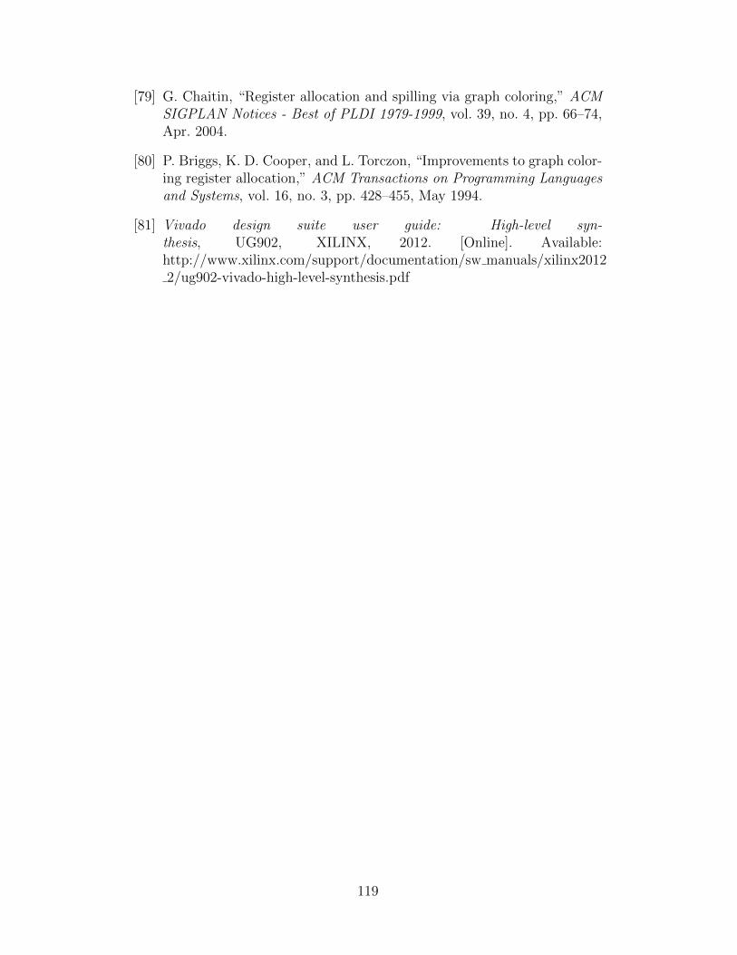
[79] G. Chaitin, “Register allocation and spilling via graph coloring,” ACMSIGPLAN Notices - Best of PLDI 1979-1999, vol. 39, no. 4, pp. 66–74,Apr. 2004.
[80] P. Briggs, K. D. Cooper, and L. Torczon, “Improvements to graph color-ing register allocation,” ACM Transactions on Programming Languagesand Systems, vol. 16, no. 3, pp. 428–455, May 1994.
[81] Vivado design suite user guide: High-level syn-thesis, UG902, XILINX, 2012. [Online]. Available:http://www.xilinx.com/support/documentation/sw manuals/xilinx20122/ug902-vivado-high-level-synthesis.pdf
119


![Tzakia Alexandros brochure 2016 - pages 16]j](https://static.fdocuments.us/doc/165x107/58ec3e3b1a28ab40458b45b7/tzakia-alexandros-brochure-2016-pages-16j.jpg)