Buffered, Fast-Settling, Dual, 12-/10-/8-Bit, Voltage ... · General Description The...
35
General Description The MAX5290–MAX5295 dual, 12-/10-/8-bit, voltage- output digital-to-analog converters (DACs) offer buffered outputs and a 3μs maximum settling time at the 12-bit level. The DACs operate from a 2.7V to 5.25V analog supply and a separate 1.8V to 3.6V digital sup- ply. The 20MHz 3-wire serial interface is compatible with SPI™, QSPI™, MICROWIRE™, and digital signal processor (DSP) protocol applications. Multiple devices can share a common serial interface in direct access or daisy-chained configuration. The MAX5290–MAX5295 provide two multifunctional, user-programmable, digital I/O ports. The externally selectable power-up states of the DAC outputs are either zero scale, midscale, or full scale. Software-selectable FAST and SLOW settling modes decrease settling time in FAST mode, or reduce supply current in SLOW mode. The MAX5290/MAX5291 are 12-bit DACs, the MAX5292/ MAX5293 are 10-bit DACs, and the MAX5294/MAX5295 are 8-bit DACs. The MAX5290/ MAX5292/MAX5294 pro- vide unity-gain-configured output buffers, while the MAX5291/MAX5293/MAX5295 provide force-sense-con- figured output buffers. The MAX5290– MAX5295 are specified over the extended -40°C to +85°C temperature range, and are available in space-saving 4mm x 4mm, 16-pin thin QFN and 6.5mm x 5mm, 14-pin and 16-pin TSSOP packages. Applications Portable Instrumentation Automatic Test Equipment (ATE) Digital Offset and Gain Adjustment Automatic Tuning Programmable Voltage and Current Sources Programmable Attenuators Industrial Process Controls Motion Control Microprocessor (μP)-Controlled Systems Power Amplifier Control Fast Parallel-DAC to Serial-DAC Upgrades Features ♦ Dual, 12-/10-/8-Bit Serial DACs in 4mm x 4mm Thin QFN and TSSOP Packages ♦ 3μs (max) 12-Bit Settling Time to 1/2 LSB ♦ Integral Nonlinearity 1 LSB (max) MAX5290/MAX5291 A-Grade (12-Bit) 1 LSB (max) MAX5292/MAX5293 (10-Bit) 1/2 LSB (max) MAX5294/MAX5295 (8-Bit) ♦ Guaranteed Monotonic, ±1 LSB (max) DNL ♦ Two User-Programmable Digital I/O Ports ♦ Single +2.7V to +5.25V Analog Supply ♦ +1.8V to AV DD Digital Supply ♦ 20MHz 3-Wire SPI-/QSPI-/MICROWIRE- and DSP-Compatible Serial Interface ♦ Glitch-Free Outputs Power Up to Zero Scale, Midscale or Full Scale ♦ Unity-Gain- or Force-Sense-Configured Output Buffers MAX5290–MAX5295 Buffered, Fast-Settling, Dual, 12-/10-/8-Bit, Voltage-Output DACs ________________________________________________________________ Maxim Integrated Products 1 Ordering Information 19-3005; Rev 3; 7/07 For pricing, delivery, and ordering information, please contact Maxim Direct at 1-888-629-4642, or visit Maxim’s website at www.maxim-ic.com. *Future product—contact factory for availability. Specifications are preliminary. **EP = Exposed paddle. Selector Guide and Pin Configurations appear at end of data sheet. SPI/QSPI are trademarks of Motorola, Inc. MICROWIRE is a trademark of National Semiconductor Corp. PART TEMP RANGE PIN-PACKAGE MAX5290AEUD -40°C to +85°C 14 TSSOP MAX5290BEUD -40°C to +85°C 14 TSSOP MAX5290AETE* -40°C to +85°C 16 Thin QFN-EP** MAX5290BETE* -40°C to +85°C 16 Thin QFN-EP** MAX5291AEUE -40°C to +85°C 16 TSSOP MAX5291BEUE -40°C to +85°C 16 TSSOP MAX5291AETE* -40°C to +85°C 16 Thin QFN-EP** MAX5291BETE* -40°C to +85°C 16 Thin QFN-EP** MAX5292EUD -40°C to +85°C 14 TSSOP MAX5292ETE* -40°C to +85°C 16 Thin QFN-EP** MAX5293EUE -40°C to +85°C 16 TSSOP MAX5293ETE* -40°C to +85°C 16 Thin QFN-EP** MAX5294EUD -40°C to +85°C 14 TSSOP MAX5294ETE* -40°C to +85°C 16 Thin QFN-EP** MAX5295EUE -40°C to +85°C 16 TSSOP MAX5295ETE* -40°C to +85°C 16 Thin QFN-EP**
Transcript of Buffered, Fast-Settling, Dual, 12-/10-/8-Bit, Voltage ... · General Description The...

General DescriptionThe MAX5290–MAX5295 dual, 12-/10-/8-bit, voltage-output digital-to-analog converters (DACs) offerbuffered outputs and a 3µs maximum settling time atthe 12-bit level. The DACs operate from a 2.7V to 5.25Vanalog supply and a separate 1.8V to 3.6V digital sup-ply. The 20MHz 3-wire serial interface is compatiblewith SPI™, QSPI™, MICROWIRE™, and digital signalprocessor (DSP) protocol applications. Multiple devicescan share a common serial interface in direct access ordaisy-chained configuration. The MAX5290–MAX5295provide two multifunctional, user-programmable, digitalI/O ports. The externally selectable power-up states ofthe DAC outputs are either zero scale, midscale, or fullscale. Software-selectable FAST and SLOW settlingmodes decrease settling time in FAST mode, or reducesupply current in SLOW mode.
The MAX5290/MAX5291 are 12-bit DACs, the MAX5292/MAX5293 are 10-bit DACs, and the MAX5294/MAX5295are 8-bit DACs. The MAX5290/ MAX5292/MAX5294 pro-vide unity-gain-configured output buffers, while theMAX5291/MAX5293/MAX5295 provide force-sense-con-figured output buffers. The MAX5290– MAX5295 arespecified over the extended -40°C to +85°C temperaturerange, and are available in space-saving 4mm x 4mm,16-pin thin QFN and 6.5mm x 5mm, 14-pin and 16-pinTSSOP packages.
ApplicationsPortable Instrumentation
Automatic Test Equipment (ATE)
Digital Offset and Gain Adjustment
Automatic Tuning
Programmable Voltage and Current Sources
Programmable Attenuators
Industrial Process Controls
Motion Control
Microprocessor (µP)-Controlled Systems
Power Amplifier Control
Fast Parallel-DAC to Serial-DAC Upgrades
Features♦ Dual, 12-/10-/8-Bit Serial DACs in 4mm x 4mm
Thin QFN and TSSOP Packages
♦ 3µs (max) 12-Bit Settling Time to 1/2 LSB
♦ Integral Nonlinearity1 LSB (max) MAX5290/MAX5291 A-Grade (12-Bit)1 LSB (max) MAX5292/MAX5293 (10-Bit)1/2 LSB (max) MAX5294/MAX5295 (8-Bit)
♦ Guaranteed Monotonic, ±1 LSB (max) DNL
♦ Two User-Programmable Digital I/O Ports
♦ Single +2.7V to +5.25V Analog Supply
♦ +1.8V to AVDD Digital Supply
♦ 20MHz 3-Wire SPI-/QSPI-/MICROWIRE- and DSP-Compatible Serial Interface
♦ Glitch-Free Outputs Power Up to Zero Scale,Midscale or Full Scale
♦ Unity-Gain- or Force-Sense-Configured OutputBuffers
MA
X5
29
0–M
AX
52
95
Buffered, Fast-Settling, Dual, 12-/10-/8-Bit,Voltage-Output DACs
________________________________________________________________ Maxim Integrated Products 1
Ordering Information
19-3005; Rev 3; 7/07
For pricing, delivery, and ordering information, please contact Maxim Direct at 1-888-629-4642,or visit Maxim’s website at www.maxim-ic.com.
*Future product—contact factory for availability. Specificationsare preliminary.
**EP = Exposed paddle.
Selector Guide and Pin Configurations appear at end of datasheet.
SPI/QSPI are trademarks of Motorola, Inc.MICROWIRE is a trademark of National Semiconductor Corp.
PART TEMP RANGE PIN-PACKAGE
MAX5290AEUD -40°C to +85°C 14 TSSOP
MAX5290BEUD -40°C to +85°C 14 TSSOP
MAX5290AETE* -40°C to +85°C 16 Thin QFN-EP**
MAX5290BETE* -40°C to +85°C 16 Thin QFN-EP**
MAX5291AEUE -40°C to +85°C 16 TSSOP
MAX5291BEUE -40°C to +85°C 16 TSSOP
MAX5291AETE* -40°C to +85°C 16 Thin QFN-EP**
MAX5291BETE* -40°C to +85°C 16 Thin QFN-EP**
MAX5292EUD -40°C to +85°C 14 TSSOP
MAX5292ETE* -40°C to +85°C 16 Thin QFN-EP**
MAX5293EUE -40°C to +85°C 16 TSSOP
MAX5293ETE* -40°C to +85°C 16 Thin QFN-EP**
MAX5294EUD -40°C to +85°C 14 TSSOP
MAX5294ETE* -40°C to +85°C 16 Thin QFN-EP**
MAX5295EUE -40°C to +85°C 16 TSSOP
MAX5295ETE* -40°C to +85°C 16 Thin QFN-EP**
MA
X5
29
0–M
AX
52
95
Buffered, Fast-Settling, Dual, 12-/10-/8-Bit,Voltage-Output DACs
2 _______________________________________________________________________________________
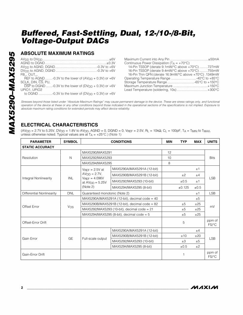
ABSOLUTE MAXIMUM RATINGS
ELECTRICAL CHARACTERISTICS(AVDD = 2.7V to 5.25V, DVDD = 1.8V to AVDD, AGND = 0, DGND = 0, VREF = 2.5V, RL = 10kΩ, CL = 100pF, TA = TMIN to TMAX,unless otherwise noted. Typical values are at TA = +25°C.) (Note 1)
Stresses beyond those listed under “Absolute Maximum Ratings” may cause permanent damage to the device. These are stress ratings only, and functionaloperation of the device at these or any other conditions beyond those indicated in the operational sections of the specifications is not implied. Exposure toabsolute maximum rating conditions for extended periods may affect device reliability.
AVDD to DVDD........................................................................±6VAGND to DGND..................................................................±0.3VAVDD to AGND, DGND.............................................-0.3V to +6VDVDD to AGND, DGND ............................................-0.3V to +6VFB_, OUT_,
REF to AGND........-0.3V to the lower of (AVDD + 0.3V) or +6VSCLK, DIN, CS, PU,
DSP to DGND .......-0.3V to the lower of (DVDD + 0.3V) or +6VUPIO1, UPIO2
to DGND ...............-0.3V to the lower of (DVDD + 0.3V) or +6V
Maximum Current into Any Pin .........................................±50mAContinuous Power Dissipation (TA = +70°C)
14-Pin TSSOP (derate 9.1mW/°C above +70°C) .........727mW16-Pin TSSOP (derate 9.4mW/°C above +70°C) .........755mW16-Pin Thin QFN (derate 16.9mW/°C above +70°C) .1349mW
Operating Temperature Range ...........................-40°C to +85°CStorage Temperature Range .............................-65°C to +150°CMaximum Junction Temperature .....................................+150°CLead Temperature (soldering, 10s) .................................+300°C
PARAMETER SYMBOL CONDITIONS MIN TYP MAX UNITS
STATIC ACCURACY
MAX5290/MAX5291 12
MAX5292/MAX5293 10Resolution N
MAX5294/MAX5295 8
Bits
MAX5290A/MAX5291A (12-bit) ±1
MAX5290B/MAX5291B (12-bit) ±2 ±4
MAX5292/MAX5293 (10-bit) ±0.5 ±1Integral Nonlinearity INL
VREF = 2.5V atAVDD = 2.7V,VREF = 4.096Vat AVDD = 5.25V(Note 2) MAX5294/MAX5295 (8-bit) ±0.125 ±0.5
LSB
Differential Nonlinearity DNL Guaranteed monotonic (Note 2) ±1 LSB
MAX5290A/MAX5291A (12-bit), decimal code = 40 ±5
MAX5290B/MAX5291B (12-bit), decimal code = 82 ±5 ±25
MAX5292/MAX5293 (10-bit), decimal code = 21 ±5 ±25Offset Error VOS
MAX5294/MAX5295 (8-bit), decimal code = 5 ±5 ±25
mV
Offset-Error Drift 5ppm ofFS/°C
MAX5290A/MAX5291A (12-bit) ±4
MAX5290B/MAX5291B (12-bit) ±10 ±20
MAX5292/MAX5293 (10-bit) ±3 ±5Gain Error GE Full-scale output
MAX5294/MAX5295 (8-bit) ±0.5 ±2
LSB
Gain-Error Drift 1ppm ofFS/°C

MA
X5
29
0–M
AX
52
95
Buffered, Fast-Settling, Dual, 12-/10-/8-Bit,Voltage-Output DACs
_______________________________________________________________________________________ 3
ELECTRICAL CHARACTERISTICS (continued)(AVDD = 2.7V to 5.25V, DVDD = 1.8V to AVDD, AGND = 0, DGND = 0, VREF = 2.5V, RL = 10kΩ, CL = 100pF, TA = TMIN to TMAX,unless otherwise noted. Typical values are at TA = +25°C.) (Note 1)
PARAMETER SYMBOL CONDITIONS MIN TYP MAX UNITS
Power-Supply RejectionRatio
PSRR Full-scale output, AVDD = 2.7V to 3.6V 200 µV/V
REFERENCE INPUT
Reference Input Range VREF 0.25 AVDD V
Reference InputResistance
RREF Normal operation (no code dependence) 145 200 kΩ
Reference LeakageCurrent
IREF Shutdown mode 0.5 1 µA
DAC OUTPUT CHARACTERISTICS
Unity gain 85SLOW mode,full scale Force sense 67
Unity gain 140Output Voltage Noise
FAST mode,full scale Force sense 110
µVRMS
Unity-gain output 0 AVDDOutput Voltage Range(Note 4) Force-sense output 0 AVDD / 2
V
DC Output Impedance 38 ΩShort-Circuit Current AVDD = 3V, OUT_ to AGND, full scale, FAST mode 45 mA
Power-Up Time From DVDD applied, interface is functional 30 60 µs
Wake-Up Time Coming out of shutdown, outputs settled 40 µs
Output OUT_ and FB_Open-Circuit LeakageCurrent
Programmed in shutdown mode, force-senseoutputs only
0.01 µA
DIGITAL OUTPUTS (UPIO_)
Output High Voltage VOH ISOURCE = 2mADVDD -
0.5V
Output Low Voltage VOL ISINK = 2mA 0.4 V
DIGITAL INPUTS (SCLK, CS, DIN, DSP, UPIO_)
DVDD ≥ 2.7V 2.4
Input High Voltage VIHDVDD < 2.7V
0.7 xDVDD
V
DVDD > 3.6V 0.8
2.7V ≤ DVDD ≤ 3.6V 0.6Input Low Voltage VIL
DVDD < 2.7V 0.2
V
Input Leakage Current IIN ±0.1 ±1 µA
Input Capacitance CIN 10 pF
MA
X5
29
0–M
AX
52
95
Buffered, Fast-Settling, Dual, 12-/10-/8-Bit,Voltage-Output DACs
4 _______________________________________________________________________________________
ELECTRICAL CHARACTERISTICS (continued)(AVDD = 2.7V to 5.25V, DVDD = 1.8V to AVDD, AGND = 0, DGND = 0, VREF = 2.5V, RL = 10kΩ, CL = 100pF, TA = TMIN to TMAX,unless otherwise noted. Typical values are at TA = +25°C.) (Note 1)
PARAMETER SYMBOL CONDITIONS MIN TYP MAX UNITS
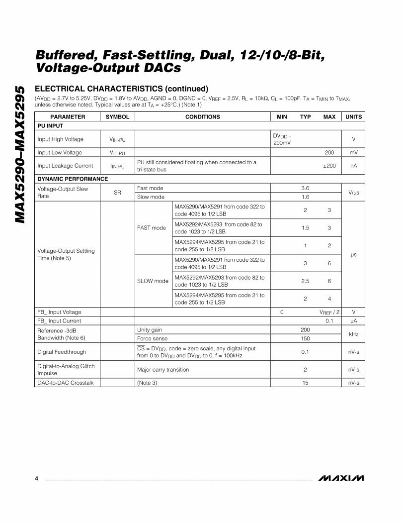
PU INPUT
Input High Voltage VIH-PUDVDD -200mV
V
Input Low Voltage VIL-PU 200 mV
Input Leakage Current IIN-PUPU still considered floating when connected to atri-state bus
±200 nA
DYNAMIC PERFORMANCE
Fast mode 3.6Voltage-Output SlewRate
SRSlow mode 1.6
V/µs
M AX 5290/M AX 5291 fr om cod e 322 tocod e 4095 to 1/2 LS B
2 3
M AX 5292/M AX 5293 fr om cod e 82 tocod e 1023 to 1/2 LS B
1.5 3FAST mode
MAX5294/MAX5295 from code 21 tocode 255 to 1/2 LSB
1 2
M AX 5290/M AX 5291 fr om cod e 322 tocod e 4095 to 1/2 LS B
3 6
MAX5292/MAX5293 from code 82 tocode 1023 to 1/2 LSB
2.5 6
Voltage-Output SettlingTime (Note 5)
SLOW mode
MAX5294/MAX5295 from code 21 tocode 255 to 1/2 LSB
2 4
µs
FB_ Input Voltage 0 VREF / 2 V
FB_ Input Current 0.1 µA
Unity gain 200Reference -3dBBandwidth (Note 6) Force sense 150
kHz
Digital FeedthroughCS = DVDD, code = zero scale, any digital inputfrom 0 to DVDD and DVDD to 0, f = 100kHz
0.1 nV-s
Digital-to-Analog GlitchImpulse
Major carry transition 2 nV-s
DAC-to-DAC Crosstalk (Note 3) 15 nV-s

MA
X5
29
0–M
AX
52
95
Buffered, Fast-Settling, Dual, 12-/10-/8-Bit,Voltage-Output DACs
_______________________________________________________________________________________ 5
ELECTRICAL CHARACTERISTICS (continued)(AVDD = 2.7V to 5.25V, DVDD = 1.8V to AVDD, AGND = 0, DGND = 0, VREF = 2.5V, RL = 10kΩ, CL = 100pF, TA = TMIN to TMAX,unless otherwise noted. Typical values are at TA = +25°C.) (Note 1)
PARAMETER SYMBOL CONDITIONS MIN TYP MAX UNITS
POWER REQUIREMENTS
Analog Supply VoltageRange
AVDD 2.70 5.25 V
Digital Supply VoltageRange
DVDD 1.8 AVDD V
Unity gain 0.55 0.8 mASLOW mode, all digital inputsat DGND or DVDD, no load,VREF = 2.5V Force sense 0.9 1.2 mA
Unity gain 0.85 2
Operating SupplyCurrent
IAVDD +IDVDD
FAST mode, all digital inputsat DGND or DVDD, no load,VREF = 2.5V Force sense 1.2 2
mA
Shutdown SupplyCurrent
IAV D D ( S H D N ) +
ID V D D ( S H D N )
No clocks, all digital inputs at DGND or DVDD, allDACs in shutdown mode
0.5 1.0 µA
TIMING CHARACTERISTICS—DSP Mode Disabled (3V, 3.3V Logic) (Figure 1)(DVDD = 2.7V to 5.25V, DGND = 0, TA = TMIN to TMAX, unless otherwise noted.)
PARAMETER SYMBOL CONDITIONS MIN TYP MAX UNITS
SCLK Frequency fSCLK 2.7V < DVDD < 5.25V 20 MHz
SCLK Pulse-Width High tCH (Note 7) 20 ns
SCLK Pulse-Width Low tCL (Note 7) 20 ns
CS Fall to SCLK Rise Setup Time tCSS 10 ns
SCLK Rise to CS Rise Hold Time tCSH 5 ns
SCLK Rise to CS Fall Setup Time tCS0 10 ns
DIN to SCLK Rise Setup Time tDS 12 ns
DIN to SCLK Rise Hold Time tDH 5 ns
SCLK Rise to DOUTDC1 ValidPropagation Delay
tDO1 CL = 20pF, UPIO_ = DOUTDC1 mode 30 ns
SCLK Fall to DOUT_ ValidPropagation Delay
tDO2CL = 20pF, UPIO_ = DOUTDC0 or DOUTRBmode
30 ns
CS Rise to SCLK Rise Hold Time tCS1 MICROWIRE and SPI modes 0 and 3 10 ns
CS Pulse-Width High tCSW 45 ns

MA
X5
29
0–M
AX
52
95
Buffered, Fast-Settling, Dual, 12-/10-/8-Bit,Voltage-Output DACs
6 _______________________________________________________________________________________
TIMING CHARACTERISTICS—DSP Mode Disabled (3V, 3.3V Logic) (Figure 1) (continued)(DVDD = 2.7V to 5.25V, DGND = 0, TA = TMIN to TMAX, unless otherwise noted.)
PARAMETER SYMBOL CONDITIONS MIN TYP MAX UNITS
UPIO TIMING CHARACTERISTICS
DOUT Tri-State Time when ExitingDOUTDC0, DOUTDC1, orDOUTRB UPIO Modes
tDOZCL = 20pF, from end of write cycle to UPIO_in high impedance
100 ns
DOUTRB Tri-State Time from CSRise
tDRBZCL = 20pF, from rising edge of CS to UPIO_in high impedance
20 ns
DOUTRB Tri-State Enable Timefrom 8th SCLK Rise
tZENCL = 20pF, from 8th rising edge of SCLK toUPIO_ driven out of tri-state
0 ns
LDAC Pulse-Width Low tLDL Figure 5 20 ns
LDAC Effective Delay tLDS Figure 6 100 ns
CLR, MID, SET Pulse-Width Low tCMS Figure 5 20 ns
GPO Output Settling Time tGP Figure 6 100 ns
GPO Output High-ImpedanceTime
tGPZ 100 ns
TIMING CHARACTERISTICS—DSP Mode Disabled (1.8V Logic) (Figure 1)(DVDD = 1.8V to 5.25V, DGND = 0, TA = TMIN to TMAX, unless otherwise noted.)
PARAMETER SYMBOL CONDITIONS MIN TYP MAX UNITS
SCLK Frequency fSCLK 1.8V < DVDD < 5.25V 10 MHz
SCLK Pulse-Width High tCH (Note 7) 40 ns
SCLK Pulse-Width Low tCL (Note 7) 40 ns
CS Fall to SCLK Rise Setup Time tCSS 20 ns
SCLK Rise to CS Rise Hold Time tCSH 0 ns
SCLK Rise to CS Fall Setup Time tCS0 10 ns
DIN to SCLK Rise Setup Time tDS 20 ns
DIN to SCLK Rise Hold Time tDH 5 ns
SCLK Rise to DOUTDC1 ValidPropagation Delay
tDO1 CL = 20pF, UPIO_ = DOUTDC1 mode 60 ns
SCLK Fall to DOUT_ ValidPropagation Delay
tDO2CL = 20pF, UPIO_ = DOUTDC0 or DOUTRBmode
60 ns
CS Rise to SCLK Rise Hold Time tCS1 MICROWIRE and SPI modes 0 and 3 20 ns
CS Pulse-Width High tCSW 90 ns

MA
X5
29
0–M
AX
52
95
Buffered, Fast-Settling, Dual, 12-/10-/8-Bit,Voltage-Output DACs
_______________________________________________________________________________________ 7
TIMING CHARACTERISTICS—DSP Mode Disabled (1.8V Logic) (Figure 1) (continued)(DVDD = 1.8V to 5.25V, DGND = 0, TA = TMIN to TMAX, unless otherwise noted.)
PARAMETER SYMBOL CONDITIONS MIN TYP MAX UNITS
UPIO_ TIMING CHARACTERISTICS
DOUT Tri-State Time whenExiting DOUTDC0, DOUTDC1, orDOUTRB UPIO Modes
tDOZCL = 20pF, from end of write cycle to UPIO_in high impedance
200 ns
DOUTRB Tri-State Time from CSRise
tDRBZCL = 20pF, from rising edge of CS to UPIO_in high impedance
40 ns
DOUTRB Tri-State Enable Timefrom 8th SCLK Rise
tZENCL = 20pF, from 8th rising edge of SCLK toUPIO_ driven out of tri-state
0 ns
LDAC Pulse-Width Low tLDL Figure 5 40 ns
LDAC Effective Delay tLDS Figure 6 200 ns
CLR, MID, SET Pulse-Width Low tCMS Figure 5 40 ns
GPO Output Settling Time tGP Figure 6 200 ns
GPO Output High-ImpedanceTime
tGPZ 200 ns
TIMING CHARACTERISTICS—DSP Mode Enabled (3V, 3.3V Logic) (Figure 2)(DVDD = 2.7V to 5.25V, DGND = 0, TA = TMIN to TMAX, unless otherwise noted.)
PARAMETER SYMBOL CONDITIONS MIN TYP MAX UNITS
SCLK Frequency fSCLK 2.7V < DVDD < 5.25V 20 MHz
SCLK Pulse-Width High tCH (Note 7) 20 ns
SCLK Pulse-Width Low tCL (Note 7) 20 ns
CS Fall to SCLK Fall Setup Time tCSS 10 ns
DSP Fall to SCLK Fall Setup Time tDSS 10 ns
SCLK Fall to CS Rise Hold Time tCSH 5 ns
SCLK Fall to CS Fall Delay tCS0 10 ns
SCLK Fall to DSP Fall Delay tDS0 10 ns
DIN to SCLK Fall Setup Time tDS 12 ns
DIN to SCLK Fall Hold Time tDH 5 ns
SCLK Rise to DOUT_ ValidPropagation Delay
tDO1CL = 20pF, UPIO_ = DOUTDC1 or DOUTRBmode
30 ns
SCLK Fall to DOUTDC0 ValidPropagation Delay
tDO2 CL = 20pF, UPIO_ = DOUTDC0 mode 30 ns
CS Rise to SCLK Fall Hold Time tCS1 MICROWIRE and SPI modes 0 and 3 10 ns
CS Pulse-Width High tCSW 45 ns
DSP Pulse-Width High tDSW 20 ns
DSP Pulse-Width Low tDSPWL (Note 8) 20 ns

MA
X5
29
0–M
AX
52
95
Buffered, Fast-Settling, Dual, 12-/10-/8-Bit,Voltage-Output DACs
8 _______________________________________________________________________________________
TIMING CHARACTERISTICS—DSP Mode Enabled (3V, 3.3V Logic) (Figure 2) (continued)(DVDD = 2.7V to 5.25V, DGND = 0, TA = TMIN to TMAX, unless otherwise noted.)
PARAMETER SYMBOL CONDITIONS MIN TYP MAX UNITS
UPIO_ TIMING CHARACTERISTICS
DOUT Tri-State Time whenExiting DOUTDC0, DOUTDC1, orDOUTRB UPIO Modes
tDOZCL = 20pF, from end of write cycle to UPIO_in high impedance
100 ns
DOUTRB Tri-State Time from CSRise
tDRBZCL = 20pF, from rising edge of CS to UPIO_in high impedance
20 ns
DOUTRB Tri-State Enable Timefrom 8th SCLK Fall
tZENCL = 20pF, from 8th falling edge of SCLK toUPIO_ driven out of tri-state
0 ns
LDAC Pulse-Width Low tLDL Figure 5 20 ns
LDAC Effective Delay tLDS Figure 6 100 ns
CLR, MID, SET Pulse-Width Low tCMS Figure 5 20 ns
GPO Output Settling Time tGP Figure 6 100 ns
GPO Output High-ImpedanceTime
tGPZ 100 ns
TIMING CHARACTERISTICS—DSP Mode Enabled (1.8V Logic) (Figure 2)(DVDD = 1.8V to 5.25V, DGND = 0, TA = TMIN to TMAX, unless otherwise noted.)
PARAMETER SYMBOL CONDITIONS MIN TYP MAX UNITS
SCLK Frequency fSCLK 1.8V < DVDD < 5.25V 10 MHz
SCLK Pulse-Width High tCH (Note 7) 40 ns
SCLK Pulse-Width Low tCL (Note 7) 40 ns
CS Fall to SCLK Fall Setup Time tCSS 20 ns
DSP Fall to SCLK Fall Setup Time tDSS 20 ns
SCLK Fall to CS Rise Hold Time tCSH 0 ns
SCLK Fall to CS Fall Delay tCS0 10 ns
SCLK Fall to DSP Fall Delay tDS0 15 ns
DIN to SCLK Fall Setup Time tDS 20 ns
DIN to SCLK Fall Hold Time tDH 5 ns
SCLK Rise to DOUT_ ValidPropagation Delay
tDO1CL = 20pF, UPIO_ = DOUTDC1 or DOUTRBmode
60 ns
SCLK Fall to DOUTDC0 ValidPropagation Delay
tDO2 CL = 20pF, UPIO_ = DOUTDC0 mode 60 ns
CS Rise to SCLK Fall Hold Time tCS1 MICROWIRE and SPI modes 0 and 3 20 ns
CS Pulse-Width High tCSW 90 ns
DSP Pulse-Width High tDSW 40 ns
DSP Pulse-Width Low tDSPWL (Note 8) 40 ns

MA
X5
29
0–M
AX
52
95
Buffered, Fast-Settling, Dual, 12-/10-/8-Bit,Voltage-Output DACs
_______________________________________________________________________________________ 9
TIMING CHARACTERISTICS—DSP Mode Enabled (1.8V Logic) (Figure 2) (continued)(DVDD = 1.8V to 5.25V, DGND = 0, TA = TMIN to TMAX, unless otherwise noted.)
PARAMETER SYMBOL CONDITIONS MIN TYP MAX UNITS
UPIO_ TIMING CHARACTERISTICS
DOUT Tri-State Time whenExiting DOUTDC0, DOUTDC1, orDOUTRB UPIO_ Modes
tDOZCL = 20pF, from end of write cycle to UPIO_in high impedance
200 ns
DOUTRB Tri-State Time from CSRise
tDRBZCL = 20pF, from rising edge of CS to UPIO_in high impedance
40 ns
DOUTRB Tri-State Enable Timefrom 8th SCLK Fall
tZENCL = 20pF, from 8th falling edge of SCLK toUPIO_ driven out of tri-state
0 ns
LDAC Pulse-Width Low tLDL Figure 5 40 ns
LDAC Effective Delay tLDS Figure 6 200 ns
CLR, MID, SET Pulse-Width Low tCMS Figure 5 40 ns
GPO Output Settling Time tGP Figure 6 200 ns
GPO Output High-ImpedanceTime
tGPZ 200 ns
Note 1: For the force-sense versions, FB_ is connected to its respective OUT_. VOUT(max) = VREF / 2, unless otherwise noted.Note 2: Linearity guaranteed from decimal code 40 to 4095 for the MAX5290A/MAX5291A (12-bit, A-grade), code 82 to 4095 for the
MAX5290B/MAX5291B (12-bit, B-grade), code 21 to 1023 for the MAX5292/MAX5293 (10-bit), and code 5 to 255 for theMAX5294/MAX5295 (8-bit).
Note 3: DAC-to-DAC crosstalk is measured as follows: outputs of DACA and DACB are set to full scale and the output of DACB ismeasured. While keeping DACB unchanged, the output of DACA is transitioned to zero scale and the ∆VOUT of DACB ismeasured. The procedure is repeated with DACA and DACB interchanged. DAC-to-DAC crosstalk is the maximum ∆VOUTmeasured.
Note 4: Represents the functional range. The linearity is guaranteed at VREF = 2.5V. See the Typical Operating Characteristics sec-tion for linearity at other voltages.
Note 5: Guaranteed by design.Note 6: The reference -3dB bandwidth is measured with a 0.1VP-P sine wave on VREF and with the input code at full scale.Note 7: In some daisy-chain modes, data is required to be clocked in on one clock edge and the shifted data clocked out on the fol-
lowing edge. In the case of a 1/2 clock-period delay, it is necessary to increase the minimum high/low clock times to 25ns(2.7V) or 50ns (1.8V).
Note 8: The falling edge of DSP starts a DSP-type bus cycle, provided that CS is also active low to select the device. DSP active lowand CS active low must overlap by a minimum of 10ns (2.7V) or 20ns (1.8V). CS can be permanently low in this mode of

MA
X5
29
0–M
AX
52
95
Buffered, Fast-Settling, Dual, 12-/10-/8-Bit,Voltage-Output DACs
10 ______________________________________________________________________________________
Typical Operating Characteristics(AVDD = DVDD = 3V, VREF = 2.5V, RL = 10kΩ, CL = 100pF, speed mode = FAST, PU = floating, TA = +25°C, unless otherwise noted.)
-0.8
-0.4
-0.6
0
-0.2
0.2
0.4
0 20001000 3000 4000 4096
INTEGRAL NONLINEARITY vs. DIGITALINPUT CODE (MAX5290A)
MAX
5290
toc0
1
INPUT CODE
INL
(LSB
)
-0.35
-0.20
-0.25
-0.30
-0.15
-0.10
-0.05
0
0.05
0.10
0.15
0 20001000 3000 4000 4096
INTEGRAL NONLINEARITY vs. DIGITALINPUT CODE (MAX5291A)
MAX
5290
toc0
2
INPUT CODE
INL
(LSB
)
INTEGRAL NONLINEARITYvs. DIGITAL INPUT CODE (12-BIT)
MAX
5290
toc0
3
DIGITAL INPUT CODE
INL
(LSB
)
307220481024
-3
-2
-1
0
1
2
3
4
-40 4096
UNITY GAINB-GRADE
INTEGRAL NONLINEARITYvs. DIGITAL INPUT CODE (10-BIT)
MAX
5290
toc0
4
DIGITAL INPUT CODE
INL
(LSB
)
768512256
-0.75
-0.50
-0.25
0
0.25
0.50
0.75
1.00
-1.000 1024
UNITY GAIN
INTEGRAL NONLINEARITYvs. DIGITAL INPUT CODE (8-BIT)
MAX
5290
toc0
5
DIGITAL INPUT CODE
INL
(LSB
)
19212864
-0.25
0
0.25
0.50
-0.500 256
UNITY GAIN
DIFFERENTIAL NONLINEARITYvs. DIGITAL INPUT CODE (12-BIT)
MAX
5290
toc0
6
DIGITAL INPUT CODE
DNL
(LSB
)
307220481024
-0.1
0
0.1
0.2
-0.20 4096
UNITY GAIN
DIFFERENTIAL NONLINEARITYvs. DIGITAL INPUT CODE (10-BIT)
MAX
5290
toc0
7
DIGITAL INPUT CODE
DNL
(LSB
)
768512256
-0.025
0
0.025
0.050
-0.0500 1024
UNITY GAIN
DIFFERENTIAL NONLINEARITYvs. DIGITAL INPUT CODE (8-BIT)
MAX
5290
toc0
8
DIGITAL INPUT CODE
DNL
(LSB
)
19212864
-0.01
0
0.01
0.02
-0.020 256
UNITY GAIN
0
0.05
0.10
0.15
0.20
0.25
0.30
0.35
0.40
-40 -15 10 35 60 85
INTEGRAL NONLINEARITYvs. TEMPERATURE (A-GRADE)
MAX
5290
toc0
9
TEMPERATURE (°C)
INL
(LSB
)
UNITY GAIN
FORCESENSE
MIDSCALE

MA
X5
29
0–M
AX
52
95
Buffered, Fast-Settling, Dual, 12-/10-/8-Bit,Voltage-Output DACs
______________________________________________________________________________________ 11
Typical Operating Characteristics (continued)(AVDD = DVDD = 3V, VREF = 2.5V, RL = 10kΩ, CL = 100pF, speed mode = FAST, PU = floating, TA = +25°C, unless otherwise noted.)
INTEGRAL NONLINEARITYvs. TEMPERATURE (12-BIT)
MAX
5290
toc1
0
TEMPERATURE (°C)
INL
(LSB
)
603510-15
-2
0
2
4
-4-40 85
UNITY GAINB-GRADE
DIFFERENTIAL NONLINEARITYvs. TEMPERATURE (12-BIT)
MAX
5290
toc1
1
TEMPERATURE (°C)
DNL
(LSB
)
603510-15
-0.1
0
0.1
0.2
-0.2-40 85
UNITY GAIN
0
0.10
0.05
0.20
0.15
0.30
0.25
0.35
0.45
0.40
0.50
1.0 2.0 2.51.5 3.0 3.5 4.0 4.5 5.0
MAX
5290
toc1
2
VREF (V)
INL
(LSB
)
INTEGRAL NONLINEARITYvs. REFERENCE VOLTAGE (MAX5290A)
0
0.2
0.1
0.4
0.3
0.6
0.5
0.7
0.9
0.8
1.0
1.0 2.0 2.51.5 3.0 3.5 4.0 4.5 5.0
INTEGRAL NONLINEARITYvs. REFERENCE VOLTAGE (MAX5291A)
MAX
5290
toc1
3
VREF (V)
INL
(LSB
)
0
0.1
0.2
0.3
0.4
0.5
0.6
0.7
0.8
-40 -15 10 35 60 85
OFFSET ERROR vs. TEMPERATURE(A-GRADE)
MAX
5290
toc1
4
TEMPERATURE (°C)
OFFS
ET E
RROR
(mV)
UNITY GAIN
FORCESENSE
CODE = 40UNITY GAIN: 1 LSB = 0.6mVFORCE SENSE: 1 LSB = 0.3mV
OFFSET ERROR vs. TEMPERATURE
MAX
5290
toc1
5
TEMPERATURE (°C)
OFFS
ET E
RROR
(LSB
)
603510-15
-8
-6
-4
-2
0
-10-40 85
FORCE SENSE
UNITY GAIN
UNITY GAIN: 1 LSB = 0.6mVFORCE SENSE: 1 LSB = 0.3mV
-0.35
-0.20
-0.25
-0.30
-0.15
-0.10
-0.05
0
0.05
0.10
0.15
-40 10-15 35 60 85
GAIN ERROR vs. TEMPERATURE (A-GRADE)
MAX
5290
toc1
6
TEMPERATURE (°C)
GAIN
ERR
OR (L
SB) UNITY GAIN
FORCESENSE
UNITY GAIN: 1 LSB = 0.6mVFORCE SENSE: 1 LSB = 0.3mV
GAIN ERROR vs. TEMPERATURE
MAX
5290
toc1
7
TEMPERATURE (°C)
GAIN
ERR
OR (L
SB)
603510-15
-8
-6
-4
-2
0
-10-40 85
FORCE SENSE
UNITY GAIN
UNITY GAIN: 1 LSB = 0.6mVFORCE SENSE: 1 LSB = 0.3mV
REFERENCE INPUT BANDWIDTHM
AX52
90 to
c18
FREQUENCY (Hz)
GAIN
(dB)
1M100k10k1k
-25
-20
-15
-10
-5
0
5
-300 10M
VREF = 0.1VP-P AT 2.5VDC

MA
X5
29
0–M
AX
52
95
Buffered, Fast-Settling, Dual, 12-/10-/8-Bit,Voltage-Output DACs
12 ______________________________________________________________________________________
Typical Operating Characteristics(TA = +25°C, unless otherwise noted.)
0.4
0.70.6
0.5
0.80.9
1.11.0
1.2
0 1024 2048 3072 4096
SUPPLY CURRENT vs. DIGITALINPUT CODE (FORCE SENSE)
MAX
5290
toc1
9
DIGITAL INPUT CODE
SUPP
LY C
URRE
NT (m
A)
SLOW MODE12-BITNO LOAD
0.30.2
0.10 0
0.1
0.2
0.3
0.4
0.5
0.6
0.7
0.8
0 1024 2048 3072 4096
SUPPLY CURRENT vs. DIGITALINPUT CODE (UNITY GAIN)
MAX
5290
toc2
0
DIGITAL INPUT CODE
SUPP
LY C
URRE
NT (m
A)
SLOW MODE12-BITNO LOAD
0.4
0.7
0.6
0.5
0.9
0.8
1.3
1.2
1.1
1.0
1.4
2.7 3.1 3.5 3.9 4.3 4.7 5.1 5.5
SUPPLY CURRENT vs. SUPPLYVOLTAGE (FORCE SENSE)
MAX
5290
toc2
1
SUPPLY VOLTAGE (V)
SUPP
LY C
URRE
NT (m
A) FAST MODE
I = IAVDD + IDVDDAVDD = DVDDNO LOAD
SLOW MODE
0
0.3
0.2
0.1
0.5
0.4
0.9
0.8
0.7
0.6
1.0
2.7 3.1 3.5 3.9 4.3 4.7 5.1 5.5
SUPPLY CURRENT vs. SUPPLYVOLTAGE (UNITY GAIN)
MAX
5290
toc2
2
SUPPLY VOLTAGE (V)
SUPP
LY C
URRE
NT (m
A) FAST MODE
I = IAVDD + IDVDDAVDD = DVDDNO LOAD
SLOW MODE
50
65
60
55
75
70
95
90
85
80
100
2.7 3.1 3.5 3.9 4.3 4.7 5.1 5.5
SHUTDOWN SUPPLY CURRENTvs. SUPPLY VOLTAGE
MAX
5290
toc2
3
SUPPLY VOLTAGE (V)
SHUT
DOW
N SU
PPLY
CUR
RENT
(nA)
FORCE SENSE
AVDD = DVDDI = IAVDD + IDVDDNO LOAD
UNITY GAIN
-5
-2
-3
-4
-1
0
1
2
3
4
5
-40 10-15 35 60 85
OFFSET ERROR vs. TEMPERATURE
MAX
5290
toc2
4
TEMPERATURE (°C)
OFFS
ET E
RROR
(LSB
)
FORCE SENSE
B-GRADEUNITY GAIN: 1 LSB = 1mVFORCE SENSE: 1 LSB = 0.5mV
UNITY GAIN
-5
-2
-3
-4
-1
0
1
2
3
4
5
-40 10-15 35 60 85
GAIN ERROR vs. TEMPERATURE
MAX
5290
toc2
5
TEMPERATURE (°C)
GAIN
ERR
OR (L
SB)
FORCE SENSE
B-GRADEUNITY GAIN: 1 LSB = 1mVFORCE SENSE: 1 LSB = 0.5mV
UNITY GAIN
1.80
1.90
1.85
2.00
1.95
2.05
2.10
2.15
2.20
-40 -20 -10-30 0 10 20 30 40
OUTPUT VOLTAGE vs. OUTPUTSOURCE/SINK CURRENT
MAX
5290
toc2
6
IOUT (mA)
OUTP
UT V
OLTA
GE (V
)
MIDSCALE
UNITY GAINVREF = 4.096V
200ns/div
MAJOR-CARRY TRANSITION GLITCH
OUT_(AC-COUPLED)10mV/div
MAX5290 toc27
CS2V/div

MA
X5
29
0–M
AX
52
95
Buffered, Fast-Settling, Dual, 12-/10-/8-Bit,Voltage-Output DACs
______________________________________________________________________________________ 13
400ns/div
SETTLING TIME POSITIVE
OUT_2V/div
MAX5290 toc28
CS2V/div
FULL-SCALE TRANSITION
400ns/div
SETTLING TIME NEGATIVE
OUT_2V/div
MAX5290 toc29
CS2V/div
FULL-SCALE TRANSITION
REFERENCE INPUT BANDWIDTH
MAX
5290
toc3
0
FREQUENCY (kHz)
GAIN
(dB)
100010010
-20
-15
-10
-5
0
5
-251 10,000
VREF = 0.1VP-P AT 4.096VDCUNITY GAIN
REFERENCE FEEDTHROUGH AT 1kHz
MAX
5290
toc3
1
FREQUENCY (kHz)5.04.53.5 4.01.5 2.0 2.5 3.01.0
-110-120-130
-100-90-80-70-60-50-40-30-22
-1420.5 5.5 100µs/div
DAC-TO-DAC CROSSTALK
OUTB1mV/div
MAX5290 toc32
OUTA2V/div
1µs/div
DIGITAL FEEDTHROUGH
OUT_(AC-COUPLED)10mV/div
MAX5290 toc33
SCLK2V/div
20µs/div
POWER-UP GLITCH
AVDD2V/div
MAX5290 toc34
OUT_1V/div
PU = FLOATING
10µs/div
EXITING SHUTDOWN TO MIDSCALE
OUT_1V/div
MAX5290 toc35
UPIO_2V/div
PU = FLOATING
Typical Operating Characteristics(TA = +25°C, unless otherwise noted.)

MA
X5
29
0–M
AX
52
95
Buffered, Fast-Settling, Dual, 12-/10-/8-Bit,Voltage-Output DACs
14 ______________________________________________________________________________________
Pin Description
PIN
MAX5290MAX5292MAX5294
MAX5291MAX5293MAX5295
THIN QFN TSSOP THIN QFN TSSOP
NAME FUNCTION
1 2 1 3 DSPClock Enable. Connect DSP to DVDD at power-up to transferdata on the rising edge of SCLK. Connect DSP to DGND atpower-up to transfer data on the falling edge of SCLK.
2 3 2 4 DIN Serial Data Input
3 4 3 5 CS Active-Low Chip-Select Input
4 5 4 6 SCLK Serial Clock Input
5 6 5 7 DVDD Digital Supply
6 7 6 8 DGND Digital Ground
7 8 7 9 AGND Analog Ground
8 9 8 10 AVDD Analog Supply
9 10 9 11 OUTB DACB Output
— — 10 12 FBB Feedback for DACB Output Buffer
10 11 11 13 REF Reference Input
— — 12 14 FBA Feedback for DACA Output Buffer
11, 13 — — — N.C. No Connection. Not internally connected.
12 12 13 15 OUTA DACA Output
14 13 14 16 PU
Power-Up State Select Input. Connect PU to DVDD to set OUTAand OUTB to full scale upon power-up. Connect PU to DGND toset OUTA and OUTB to zero upon power-up. Leave PU floatingto set OUTA and OUTB to midscale upon power-up.
15 14 15 1 UPIO2 User-Programmable Input/Output 2
16 1 16 2 UPIO1 User-Programmable Input/Output 1
— — — — EPExposed Paddle (QFN Only). Not internally connected. Do notconnect to circuitry.

MA
X5
29
0–M
AX
52
95
Buffered, Fast-Settling, Dual, 12-/10-/8-Bit,Voltage-Output DACs
______________________________________________________________________________________ 15
Functional Diagrams
MAX5290MAX5292MAX5294
DOUTREGISTER
16-BIT SHIFTREGISTER
CSSCLK
DIN
DSP
SERIALINTERFACECONTROL
MUX
AVDD
UPIO1UPIO2
REF
PU
UPIO1 ANDUPIO2LOGIC POWER-DOWN
LOGIC ANDREGISTER
DECODECONTROL
INPUTREGISTER
DACREGISTER DAC A
OUTA
INPUTREGISTER DAC B
OUTB
DACREGISTER
DVDD AGND DGND

MA
X5
29
0–M
AX
52
95
Buffered, Fast-Settling, Dual, 12-/10-/8-Bit,Voltage-Output DACs
16 ______________________________________________________________________________________
Functional Diagrams (continued)
MAX5291MAX5293MAX5295
DOUTREGISTER
16-BIT SHIFTREGISTER
CSSCLK
DIN
DSP
SERIALINTERFACECONTROL
MUX
AVDD
UPIO1UPIO2
REF
PU
UPIO1 ANDUPIO2LOGIC POWER-DOWN
LOGIC ANDREGISTER
DECODECONTROL
INPUTREGISTER
DACREGISTER DAC A
OUTA
FBA
INPUTREGISTER DAC B
OUTB
FBB
DACREGISTER
DVDD AGND DGND

MA
X5
29
0–M
AX
52
95
Buffered, Fast-Settling, Dual, 12-/10-/8-Bit,Voltage-Output DACs
______________________________________________________________________________________ 17
Detailed DescriptionThe MAX5290–MAX5295 dual, 12-/10-/8-bit, voltage-output digital-to-analog converters (DACs) offerbuffered outputs and a 3µs maximum settling time atthe 12-bit level. The DACs operate from a single 2.7V to5.25V analog supply and a separate 1.8V to AVDD digi-tal supply. The MAX5290–MAX5295 include an inputregister and DAC register for each channel and a 16-bit data-in/data-out shift register. The 3-wire serialinterface is compatible with SPI, QSPI, MICROWIRE,and DSP applications. The MAX5290–MAX5295 pro-vide two user-programmable digital I/O ports, whichare programmed through the serial interface. The exter-nally selectable power-up states of the DAC outputsare either zero scale, midscale, or full scale.
Reference InputThe reference input, REF, accepts both AC and DC val-ues with a voltage range extending from 0.25V toAVDD. The voltage at REF (VREF) sets the full-scale out-put of the DACs. Determine the output voltage usingthe following equation:
Unity-gain versions:
VOUT_ = (VREF x CODE) / 2N
Force-sense versions (FB_ connected to OUT_):
VOUT = 0.5 x (VREF x CODE) / 2N
where CODE is the numeric value of the DAC’s binaryinput code and N is the bits of resolution. For theMAX5290/MAX5291, N = 12 and CODE ranges from 0to 4095. For the MAX5292/MAX5293, N = 10 andCODE ranges from 0 to 1023. For the MAX5294/MAX5295, N = 8 and CODE ranges from 0 to 255.
Output BuffersThe DACA and DACB output-buffer amplifiers of theMAX5290–MAX5295 are unity-gain stable with rail-to-rail output voltage swings and a typical slew rate of5.7V/µs. The MAX5290/MAX5292/MAX5294 provideunity-gain outputs, while the MAX5291/MAX5293/MAX5295 provide force-sense outputs. For theMAX5291/MAX5293/MAX5295, access to the outputamplifier’s inverting input provides flexibility in outputgain sett ing and signal conditioning (see theApplications Information section).
The MAX5290–MAX5295 offer FAST and SLOW-settlingtime modes. In the FAST mode, the settling time is 3µs(max), and the supply current is 2mA (max). In the SLOWmode, the settling time is 6µs (max), and the supply cur-rent drops to 0.8mA (max). See the Digital Interface sec-tion for settling-time mode programming details.
Use the serial interface to set the shutdown outputimpedance of the amplifiers to 1kΩ or 100kΩ for theMAX5290/MAX5292/MAX5294 and 1kΩ or high imped-ance for the MAX5291/MAX5293/MAX5295. The DACoutputs can drive a 2kΩ (typ) load and are stable withup to 500pF (typ) of capacitive load.
Power-On ResetAt power-up, all DAC outputs power up to full scale,midscale, or zero scale, depending on the configurationof the PU input. Connect PU to DVDD to set OUT_ to fullscale upon power-up. Connect PU to DGND to setOUT_ to zero scale upon power-up. Leave PU floatingto set OUT_ to midscale.
Digital InterfaceThe MAX5290–MAX5295 use a 3-wire serial interfacethat is compatible with SPI, QSPI, MICROWIRE, andDSPs (Figures 1 and 2). Connect DSP to DVDD beforepower-up to clock data in on the rising edge of SCLK.Connect DSP to DGND before power-up to clock data inon the falling edge of SCLK. After power-up, the deviceenters DSP frame sync mode on the first rising edge ofDSP. Refer to the Programmer’s Handbook for details.
Each MAX5290–MAX5295 includes a 16-bit input shiftregister. The data is loaded into the input shift registerthrough the serial interface. The 16 bits can be sent intwo serial 8-bit packets or one 16-bit word (CS mustremain low until all 16 bits are transferred). The data isloaded MSB first. For the MAX5290/MAX5291, the 16bits consist of 4 control bits (C3–C0) and 12 data bits(D11–D0) (see Table 1). For the 10-bit MAX5292/MAX5293 devices, D11–D2 are the data bits and D1and D0 are sub-bits. For the 8-bit MAX5294/MAX5295 devices, D11–D4 are the data bits andD3–D0 are sub-bits. Set all sub-bits to zero for optimumperformance.
Each DAC channel includes two registers: an input reg-ister and the DAC register. At power-up, the DAC out-put is set according to the state of PU. The DACs aredouble-buffered, which allows any of the following foreach channel:
• Loading the input register without updating the DACregister
• Loading the DAC register without updating the inputregister
• Updating the DAC register from the input register
• Updating the input and DAC registers simultaneously
MA
X5
29
0–M
AX
52
95
Buffered, Fast-Settling, Dual, 12-/10-/8-Bit,Voltage-Output DACs
18 ______________________________________________________________________________________
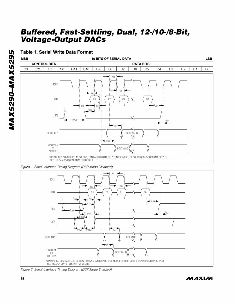
Table 1. Serial Write Data FormatMSB 16 BITS OF SERIAL DATA LSB
CONTROL BITS DATA BITS
C3 C2 C1 C0 D11 D10 D9 D8 D7 D6 D5 D4 D3 D2 D1 D0
Figure 1. Serial-Interface Timing Diagram (DSP Mode Disabled)
Figure 2. Serial-Interface Timing Diagram (DSP Mode Enabled)
SCLK
DIN
CS
DOUTDC1*
DOUTDC0OR
DOUTRB*
*UPIO1/UPIO2 CONFIGURED AS DOUTDC_ (DAISY-CHAIN DATA OUTPUT, MODE 0 OR 1) OR DOUTRB (READ-BACK DATA OUTPUT). SEE THE DATA OUTPUT SECTION FOR DETAILS.
tCH
tDS
tCS0 tDH tCSH
tDO1
tDO2
tCL
C2C3 C1 D0
tCSW tCS1
DOUT VALID
DOUT VALID
tCSS
SCLK
DIN
CS
DOUTDC0*
DOUTDC1OR
DOUTRB*
DSP
*UPIO1/UPIO2 CONFIGURED AS DOUTDC_ (DAISY-CHAIN DATA OUTPUT, MODE 0 OR 1) OR DOUTRB (READ-BACK DATA OUTPUT). SEE THE DATA OUTPUT SECTION FOR DETAILS.
tCL
tDS
tCSS
tDSW tDSPWL tD02
tD01
tDHtCS0
tCH
C3 C2 C1 D0
tCSH
tCSW
tDSStCS1
tDS0
DOUT VALID
DOUT VALID

MA
X5
29
0–M
AX
52
95
Buffered, Fast-Settling, Dual, 12-/10-/8-Bit,Voltage-Output DACs
______________________________________________________________________________________ 19
SCLKDIN
C3 C2 C1 C0 D11 D10 D9 D8 D7 D6 D5 D4 D3 D2 D1 D0DIN
SCLK
DVDD
COMMAND TAKES EFFECT HEREONLY IF SCLK COUNT = N 16
COMMAND TAKES EFFECT HEREONLY IF SCLK COUNT = N 16
MICROWIRE OR SPI (CPOL = 0, CPHA = 0) 8-BIT CONTROL DATA OR 12-BIT DAC DATA WRITE:
CS MUST REMAIN LOW BETWEEN BYTES ON A 16-BIT WRITE OPERATION
SPI (CPOL = 1, CPHA = 1) 8-BIT CONTROL DATA OR 12-BIT DAC DATA WRITE:
CS MUST REMAIN LOW BETWEEN BYTES ON A 16-BIT WRITE OPERATION
DIN
SCLK
CS
CS
MAX5290–MAX5295VDD
VDDMICROWIRE
SKSO
I/O
SCLKDIN
DVDD
MAX5290–MAX5295VDD
VDDSPI OR QSPI
SCKMOSI
SS OR I/O CS
DSPDSP
CS
C3 C2 C1 C0 D11 D10 D9 D8 D7 D6 D5 D4 D3 D2 D1 D0
SCLKDIN
C3 C2 C1 C0 D11 D10 D9 D8 D7 D6 D5 D4 D3 D2 D1 D0
C3 C2 C1 C0 D11 D10 D9 D8 D7 D6 D5 D4 D3 D2 D1 D0
DIN
SCLK
DGND
COMMAND TAKES EFFECT HEREONLY IF SCLK COUNT = N 16
COMMAND TAKES EFFECT HEREONLY IF SCLK COUNT = N 16
DSP OR SPI (CPOL = 0, CPHA = 1) 8-BIT CONTROL DATA OR 12-BIT DAC DATA WRITE:
DSP OR SPI (CPOL = 1, CPHA = 0) 8-BIT CONTROL DATA OR 12-BIT DAC DATA WRITE:
DIN
SCLK
CS
CS
MAX5290–MAX5295VSS
DSP
TCLK, SCLK, OR CLKXDT OR DX
TFS OR FSX
SCLKDIN
DGNDMAX5290–MAX5295VSS
SPI OR QSPI
SCKMOSI
SS OR I/O CS
DSPDSP
CS
CS MUST REMAIN LOW BETWEEN BYTES ON A 16-BIT WRITE OPERATION
CS MUST REMAIN LOW BETWEEN BYTES ON A 16-BIT WRITE OPERATION
Figure 3. MICROWIRE and SPI (CPOL = 0, CPHA = 0 or CPOL = 1, CPHA = 1) DAC Writes
Figure 4. DSP and SPI (CPOL = 0, CPHA = 1 or CPOL = 1, CPHA = 0) DAC Writes
Serial-Interface Programming CommandsTables 2a, 2b, and 2c provide all of the serial-interfaceprogramming commands for the MAX5290–MAX5295.Table 2a shows the basic DAC programming com-mands, Table 2b gives the advanced-feature program-ming commands, and Table 2c provides the 24-bitread commands. Figures 3 and 4 illustrate the serial-interface diagrams for read and write operations.
Loading Input and DAC RegistersThe MAX5290–MAX5295 contain a 16-bit shift registerthat is followed by a 12-bit input register and a 12-bitDAC register for each channel (see the FunctionalDiagrams). Tables 3, 4, and 5 highlight a few of the com-mands for the loading of the input and DAC registers.See Table 2a for all DAC programming commands.

MA
X5
29
0–M
AX
52
95
Buffered, Fast-Settling, Dual, 12-/10-/8-Bit,Voltage-Output DACs
20 ______________________________________________________________________________________
CO
NT
RO
L B
ITS
DA
TA
BIT
SD
AT
AC
3C
2C
1C
0D
1D
1D
9D
8D
7D
6D
5D
4D
3D
2D
1D
0F
UN
CT
ION
LO
AD
ING
INP
UT
AN
D D
AC
RE
GIS
TE
RS
A A
ND
B
DIN
00
00
D11
D10
D9
D8
D7
D6
D5
D4
D3/
0D
2/0
D1/
0D
0/0
Load
inp
ut r
egis
ter
A fr
om s
hift
reg
iste
r; D
AC
reg
iste
rs a
re u
ncha
nged
. DA
C o
utp
uts
are
unch
ang
ed.*
DIN
00
01
D11
D10
D9
D8
D7
D6
D5
D4
D3/
0D
2/0
D1/
0D
0/0
Load
DA
C r
egis
ter
A fr
om s
hift
reg
iste
r; in
put
reg
iste
rs a
re u
ncha
nged
. DA
C o
utp
uts
are
upd
ated
.*
DIN
00
10
D11
D10
D9
D8
D7
D6
D5
D4
D3/
0D
2/0
D1/
0D
0/0
Load
inp
ut r
egis
ter
A a
nd D
AC
reg
iste
r A
from
shift
reg
iste
r. D
AC
out
put
s ar
e up
dat
ed.*
DIN
00
11
D11
D10
D9
D8
D7
D6
D5
D4
D3/
0D
2/0
D1/
0D
0/0
Load
inp
ut r
egis
ter
B; D
AC
reg
iste
rs a
reun
chan
ged
. DA
C o
utp
uts
are
unch
ang
ed.*
DIN
01
00
D11
D10
D9
D8
D7
D6
D5
D4
D3/
0D
2/0
D1/
0D
0/0
Load
DA
C r
egis
ter
B fr
om s
hift
reg
iste
r; in
put
reg
iste
rs a
re u
ncha
nged
. DA
C o
utp
uts
are
upd
ated
.*
DIN
01
01
D11
D10
D9
D8
D7
D6
D5
D4
D3/
0D
2/0
D1/
0D
0/0
Load
inp
ut r
egis
ter
B a
nd D
AC
reg
iste
r B
from
shift
reg
iste
r. D
AC
out
put
s ar
e up
dat
ed.*
DIN
01
10
XX
XX
XX
XX
XX
XX
Com
man
d is
igno
red
.
DIN
01
11
XX
XX
XX
XX
XX
XX
Com
man
d is
igno
red
.
DIN
10
00
XX
XX
XX
XX
XX
XX
Com
man
d is
igno
red
.
DIN
10
01
XX
XX
XX
XX
XX
XX
Com
man
d is
igno
red
.
DIN
10
10
XX
XX
XX
XX
XX
XX
Com
man
d is
igno
red
.
DIN
10
11
XX
XX
XX
XX
XX
XX
Com
man
d is
igno
red
.
DIN
11
00
D11
D10
D9
D8
D7
D6
D5
D4
D3/
0D
2/0
D1/
0D
0/0
Load
all
inp
ut r
egis
ters
from
the
shift
reg
iste
r; a
llD
AC
reg
iste
rs a
re u
ncha
nged
. All
DA
C o
utp
uts
are
unch
ang
ed.*
DIN
11
01
D11
D10
D9
D8
D7
D6
D5
D4
D3/
0D
2/0
D1/
0D
0/0
Load
all
inp
ut a
nd D
AC
reg
iste
rs fr
om s
hift
reg
iste
r. D
AC
out
put
s ar
e up
dat
ed.*
Tab
le 2
a. D
AC
Pro
gra
mm
ing
Co
mm
and
s
X =
Don
’t ca
re.
*For
the
MA
X52
92/M
AX
5293
(10
-bit
vers
ion)
, D11
–D2
are
the
sig
nific
ant b
its a
nd D
1 an
d D
0 ar
e su
b-b
its. F
or th
e M
AX
5294
/MA
X52
95 (
8-b
it ve
rsio
n),
D11
–D4
are
the
sig
nific
ant b
its a
nd D
3–D
0 ar
e su
b-b
its. S
et a
ll su
b-b
its to
zer
o d
urin
g th
e w
rite
com
man
ds.

MA
X5
29
0–M
AX
52
95
Buffered, Fast-Settling, Dual, 12-/10-/8-Bit,Voltage-Output DACs
______________________________________________________________________________________ 21
CO
NT
RO
L B
ITS
DA
TA
BIT
SD
AT
AC
3C
2C
1C
0D
1D
1D
9D
8D
7D
6D
5D
4D
3D
2D
1D
0F
UN
CT
ION
SE
LE
CT
BIT
S
DIN
11
10
00
XX
XX
XX
XX
MB
MA
Load
DA
C r
egis
ter
A fr
omin
put
reg
iste
r A
whe
n M
Ais
1. D
AC
reg
iste
r A
isun
chan
ged
if M
A is
0.
Load
DA
C r
egis
ter
B fr
omin
put
reg
iste
r B
whe
n M
Bis
1. D
AC
reg
iste
r B
isun
chan
ged
if M
B is
0.
SH
UT
DO
WN
-MO
DE
BIT
S
DIN
11
10
01
0X
XX
XX
PD
B1
PD
B0
PD
A1
PD
A0
Writ
e D
AC
A a
nd D
AC
Bsh
utd
own
mod
e b
its. S
eeTa
ble
8.
DIN
11
10
01
1X
XX
XX
XX
XX
DO
UTR
BX
XX
XX
XX
XX
XX
XP
DB
1P
DB
0P
DA
1P
DA
0R
ead
DA
CA
and
DA
CB
shut
dow
n m
ode
bits
.
UP
IO C
ON
FIG
UR
AT
ION
BIT
S
DIN
11
10
10
0X
UP
SL2
UP
SL1
UP
3U
P2
UP
1U
P0
XX
Writ
e U
PIO
con
figur
atio
nb
its. S
ee T
able
s 19
and
22.
DIN
11
10
10
1X
XX
XX
XX
XX
DO
UTR
BX
XX
XX
XX
XU
P3-
2U
P2-
2U
P1-
2U
P0-
2U
P3-
1U
P2-
1U
P1-
1U
P0-
1R
ead
UP
IO c
onfig
urat
ion
bits
.
SE
TT
LIN
G-T
IME
-MO
DE
BIT
S
DIN
11
10
11
0X
XX
XX
XX
SP
DB
SP
DA
Writ
e D
AC
A a
nd D
AC
Bse
ttlin
g-t
ime
mod
e b
its.
DIN
11
10
11
1X
XX
XX
XX
XX
DO
UTR
BX
XX
XX
XX
XX
XX
XX
XS
PD
BS
PD
AR
ead
DA
CA
and
DA
CB
settl
ing
-tim
e m
ode
bits
.
CP
OL
AN
D C
PH
A C
ON
TR
OL
BIT
S
DIN
11
11
00
00
XX
XX
XX
CP
OL
CP
HA
Writ
e C
PO
L, C
PH
A c
ontr
olb
its. S
ee T
able
15.
DIN
11
11
00
01
XX
XX
XX
XX
DO
UTR
BX
XX
XX
XX
XX
XX
XX
XC
PO
LC
PH
AR
ead
CP
OL,
CP
HA
con
trol
bits
.
Tab
le 2
b. A
dva
nce
d-F
eatu
re P
rog
ram
min
g C
om
man
ds
X =
Don
’t ca
re.

MA
X5
29
0–M
AX
52
95
Buffered, Fast-Settling, Dual, 12-/10-/8-Bit,Voltage-Output DACs
22 ______________________________________________________________________________________
CO
NT
RO
L B
ITS
DA
TA
BIT
SD
AT
AC
3C
2C
1C
0D
27D
26D
25D
24D
23D
22D
21D
20D
19D
18D
17D
16D
15D
14D
13D
12D
11D
10D
9D
8D
7D
6D
5D
4D
3D
2D
1D
0F
UN
CT
ION
RE
AD
INP
UT
AN
D D
AC
RE
GIS
TE
RS
A A
ND
B
DIN
11
11
01
0X
11
11
11
11
11
11
11
11
XX
XX
XX
XX
D O
U TR
BX
XX
XX
XX
XD
23D
22D
21D
20D
19D
18D
17D
16D
15/
XD
14/
XD
13/
XD
12/
XD
11D
10D
9D
8D
7D
6D
5D
4D
3/ XD
2/ XD
1/ XD
0/ X
Rea
d i n
p ut
r eg
i ste
r Aan
d D
AC
r e
g i s
ter A
( al l
24b
i ts) .*
*†D
IN1
11
10
11
X1
11
11
11
11
11
11
11
1X
XX
XX
XX
X
D O
U TR
BX
XX
XX
XX
XD
23D
22D
21D
20D
19D
18D
17D
16D
15/
XD
14/
XD
13/
XD
12/
XD
11D
10D
9D
8D
7D
6D
5D
4D
3/ XD
2/ XD
1/ XD
0/ X
Rea
d i n
p ut
r eg
i ste
r Ban
d D
AC
r e
g i s
ter B
( al l
24b
i ts) .*
* †
Tab
le 2
c. 2
4-B
it R
ead
Co
mm
and
s
X=
Don
’t ca
re.
**D
23–D
12 r
epre
sent
the
12-b
it d
ata
from
the
corr
esp
ond
ing
DA
C r
egis
ter.
D11
–D0
rep
rese
nt th
e 12
-bit
dat
a fr
om th
e co
rres
pon
din
g in
put
reg
iste
r. F
orth
e M
AX
5292
/MA
X52
93, b
its D
13, D
12, D
1, a
nd D
0 ar
e d
on’t-
care
bits
. For
the
MA
X52
94/M
AX
5295
, bits
D15
–D12
and
D3–
D0
are
don
’t-ca
re b
its.
† Dur
ing
rea
db
ack,
all
ones
(co
de
FF)
mus
t be
cloc
ked
into
DIN
for
all 2
4 b
its. N
o co
mm
and
may
be
issu
ed b
efor
e al
l 24
bits
hav
e b
een
cloc
ked
out
. CS
mus
t be
kep
t low
whi
le a
ll 24
bits
are
clo
cked
out
.
CO
NT
RO
L B
ITS
DA
TA
BIT
SD
AT
AC
3C
2C
1C
0D
1D
1D
9D
8D
7D
6D
5D
4D
3D
2D
1D
0F
UN
CT
ION
UP
IO_
AS
GP
I (G
EN
ER
AL
-PU
RP
OS
E IN
PU
T)
DIN
11
11
00
1X
XX
XX
XX
XX
DO
UTR
BX
XX
XX
XX
XX
XR
TP2
LF2
LR2
RTP
1LF
1LR
1
Rea
d U
PIO
_ in
put
s. (
Val
idon
ly w
hen
UP
IO1
orU
PIO
2 is
con
figur
ed a
s a
gen
eral
-pur
pos
e in
put
.)S
ee G
PI,
GP
OL,
GP
OH
sect
ion.
OT
HE
R C
OM
MA
ND
S
DIN
11
11
10
0X
XX
XX
XX
XX
Com
man
d is
igno
red
.
DIN
11
11
10
1X
XX
XX
XX
XX
Com
man
d is
igno
red
.
DIN
11
11
11
0X
XX
XX
XX
XX
Com
man
d is
igno
red
.
DIN
11
11
11
10
XX
XX
XX
XX
Com
man
d is
igno
red
.
DIN
11
11
11
11
11
11
11
11
16-b
it no
-op
com
man
d. A
llD
AC
s ar
e un
affe
cted
.
Tab
le 2
b. A
dva
nce
d-F
eatu
re P
rog
ram
min
g C
om
man
ds
(co
nti
nu
ed)
X=
Don
’t ca
re.

MA
X5
29
0–M
AX
52
95
Buffered, Fast-Settling, Dual, 12-/10-/8-Bit,Voltage-Output DACs
______________________________________________________________________________________ 23
Default register values at power-up correspond to thestate of PU, e.g. input and DAC registers are set to800hex if PU is floating, FFFhex if PU = DVDD, and000hex if PU= DGND.
DAC Programming Examples:To load input register A from the shift register, leavingDAC register A unchanged (DAC output unchanged),use the command in Table 3.
The MAX5290–MAX5295 can load DAC register A fromthe shift register, leaving input register A unchanged,by using the command in Table 4.
To load input register A and DAC register A simultane-ously from the shift register, use the command in Table 5.
For the 10-bit and 8-bit versions, set sub-bits = 0 forbest performance.
Advanced Feature Programming Commands
Refer to the Programmer’s Handbook for details.
Select Bits (MA, MB)The select bits allow synchronous updating of any com-bination of channels. The select bits command theloading of the DAC register from the input register ofeach channel. Set the select bit M_ = 1 to load the DACregister “_” with data from the input register “_”, where“_” is replaced with A or B depending on the selectedchannel. Setting the select bit to M_ = 0 results in noaction for that channel (Table 6).
Table 3. Load Input Register A from Shift Register
Table 4. Load DAC Register A from Shift Register
Table 5. Load Input Register A and DAC Register A from Shift Register
Table 6. Select Command
DATA CONTROL BITS DATA BITS
DIN 0 0 0 0 D11 D10 D9 D8 D7 D6 D5 D4 D3/0 D2/0 D1/0 D0/0
DATA CONTROL BITS DATA BITS
DIN 0 0 0 1 D11 D10 D9 D8 D7 D6 D5 D4 D3/0 D2/0 D1/0 D0/0
DATA CONTROL BITS DATA BITS
DIN 0 0 1 0 D11 D10 D9 D8 D7 D6 D5 D4 D3/0 D2/0 D1/0 D0/0
DATA CONTROL BITS DATA BITS
DIN 1 1 1 0 0 0 X X X X X X X X MB MA
Table 7. Select Bits Programming ExampleDATA CONTROL BITS DATA BITS
DIN 1 1 1 0 0 0 X X X X X X X X 1 0
X = Don’t care.
X = Don’t care.

MA
X5
29
0–M
AX
52
95
Buffered, Fast-Settling, Dual, 12-/10-/8-Bit,Voltage-Output DACs
24 ______________________________________________________________________________________
Table 9. Shutdown-Mode Write Command
Table 10. Shutdown-Mode Bits Write Example
Table 11. Shutdown-Mode Read Command
DATA CONTROL BITS DATA BITS
DIN 1 1 1 0 0 1 0 X X X X X PDB1 PDB0 PDA1 PDA0
DATA CONTROL BITS DATA BITS
DIN 1 1 1 0 0 1 0 X X X X X 0 1 0 0
DATA CONTROL BITS DATA BITS
DIN 1 1 1 0 0 1 1 X X X X X X X X X
DOUTRB X X X X X X X X X X X X PDB1 PDB0 PDA1 PDA0
X = Don’t care.
X = Don’t care.
Table 12. Settling-Time-Mode Write CommandDATA CONTROL BITS DATA BITS
DIN 1 1 1 0 1 1 0 X X X X X X X SPDB SPDA
X = Don’t care.
X = Don’t care.
Select Bits Programming Example:To load DAC register B from input register B whilekeeping channel A unchanged, set MB = 1 and MA =0, as in the command in Table 7.
Shutdown-Mode Bits (PDA0, PDA1, PDB0, PDB1)Use the shutdown-mode bits to shut down each DACindependently. Set PD_0 and PD_1 according to Table8 to select the shutdown mode for DAC_, where “_” isreplaced with A or B depending on the selected chan-nel. The three possible states for unity-gain versionsare 1) normal operation, 2) shutdown with 1kΩ outputimpedance, and 3) shutdown with 100kΩ output imped-ance. The three possible states for force-sense ver-sions are 1) normal operation, 2) shutdown with 1kΩoutput impedance, and 3) shutdown with high-imped-ance output. Table 9 shows the command for writing tothe shutdown mode bits.
Shutdown-Mode Bits Write Example:To put a unity-gain version’s DACA into shutdownmode with internal 1kΩ termination to ground andDACB into the shutdown mode with the internal 100kΩtermination to ground, use the command in Table 10(applicable to unity-gain output only).
To read back the shutdown-mode bits, use the com-mand in Table 11.
Table 8. Shutdown-Mode BitsPD_1 PD_0 DESCRIPTIONS
0 0Shutdown with 1kΩ termination to groundon DAC_ output.
0 1
Shutdown with 100kΩ termination toground on DAC_ output for unity-gainversions. Shutdown with high-impedanceoutput for force-sense versions.
1 0 Ignored.
1 1DAC_ is powered up in its normal operatingmode.

MA
X5
29
0–M
AX
52
95
Buffered, Fast-Settling, Dual, 12-/10-/8-Bit,Voltage-Output DACs
______________________________________________________________________________________ 25
Settling-Time-Mode Bits (SPDA, SPDB)The settling-time-mode bits select the settling time(FAST mode or SLOW mode) of the MAX5290–MAX5295. Set SPD_ = 1 to select FAST mode or setSPD_ = 0 to select SLOW mode, where “_” is replacedby A or B, depending on the selected channel (seeTable 12). FAST mode provides a 3µs maximum set-tling time and SLOW mode provides a 10µs maximumsettling time. Default settling-time mode bits are [0, 0](SLOW mode for both DACs).
Settling-Time-Mode Write Example:To configure DACA into FAST mode and DACB intoSLOW mode, use the command in Table 13.
To read back the settling-time-mode bits, use the com-mand in Table 14.
CPOL and CPHA Control BitsThe CPOL and CPHA control bits of theMAX5290–MAX5295 are defined the same as the CPOLand CPHA bits in the SPI standard. Set the CPOL = 0and CPHA = 0 or set CPOL = 1 and CPHA = 1 forMICROWIRE and SPI applications requiring the clockingof data in on the rising edge of SCLK. Set the CPOL = 0
Table 13. Settling-Time-Mode Write ExampleDATA CONTROL BITS DATA BITS
DIN 1 1 1 0 1 1 0 X X X X X X X 0 1
X = Don’t care.
Table 14. Settling-Time-Mode Read CommandDATA CONTROL BITS DATA BITS
DIN 1 1 1 0 1 1 1 X X X X X X X X X
DOUTRB X X X X X X X X X X X X X X SPDB SPDA
Table 17. CPOL and CPHA Read CommandDATA CONTROL BITS DATA BITS
DIN 1 1 1 1 0 0 0 1 X X X X X X X X
DOUTRB X X X X X X X X X X X X X X CPOL CPHA
Table 15. CPOL and CPHA BitsCPOL CPHA DESCRIPTION
0 0Default values at power-up when DSP is connected to DVDD. Data is clocked in on the rising edgeof SCLK.
0 1Default values at power-up when DSP is connected to DGND. Data is clocked in on the falling edgeof SCLK.
1 0 Data is clocked in on the falling edge of SCLK.
1 1 Data is clocked in on the rising edge of SCLK.
Table 16. CPOL and CPHA Write CommandDATA CONTROL BITS DATA BITS
DIN 1 1 1 1 0 0 0 0 X X X X X X CPOL CPHA
X = Don’t care.
X = Don’t care.
X = Don’t care.

MA
X5
29
0–M
AX
52
95
Buffered, Fast-Settling, Dual, 12-/10-/8-Bit,Voltage-Output DACs
26 ______________________________________________________________________________________
Table 20. UPIO Programming ExampleDATA CONTROL BITS DATA BITS
DIN 1 1 1 0 1 0 0 X 0 1 0 0 0 0 X X
X = Don’t care.
Table 21. UPIO Read Command
DATA CONTROL BITS DATA BITS
DIN 1 1 1 0 1 0 1 X X X X X X X X X
DOUTRB X X X X X X X X UP3-2 UP2-2 UP1-2 UP0-2 UP3-1 UP2-1 UP1-1 UP0-1
X = Don’t care.
and CPHA = 1 or set CPOL = 1 and CPHA = 0 for DSPand SPI applications requiring the clocking of data in onthe falling edge of SCLK (refer to the Programmer’sHandbook and see Table 15 for details). At power-up, ifDSP = DVDD, the default value of CPHA is zero and ifDSP = DGND, the default value of CPHA is one. Thedefault value of CPOL is zero at power-up.
To write to the CPOL and CPHA bits, use the commandin Table 16.
To read back the device’s CPOL and CPHA bits, usethe command in Table 17.
UPIO Bits (UPSL1, UPSL2, UP0–UP3)The MAX5290–MAX5295 provide two user-programma-ble input/output (UPIO) ports: UPIO1 and UPIO2. Theseports have 15 possible configurations, as shown inTable 22. UPIO1 and UPIO2 can be programmed inde-pendently or simultaneously by writing to the UPSL1,UPSL2, and UP0–UP3 bits (see Table 18).
Table 19 shows how UPIO1 and UPIO2 are selected forconfiguration. The UP0–UP3 bits select the desiredfunctions for UPIO1 and/or UPIO2 (see Table 22).
Default states of UP10_ are high impedance. If usingUP10_, connect 10kΩ pullup resistors from each UPIOpin to DVDD.
UPIO Programming Example:To set only UPIO1 as LDAC and leave UPIO2unchanged, write the command in Table 20.
The UPIO selection and configuration bits can be readback from the MAX5290–MAX5295 when UPIO1 orUPIO2 is configured as a DOUTRB output. Table 21shows the read-back data format for the UPIO bits.Writing a 1110 101X XXXX XXXX initiates a read operationof the UPIO bits. The data is clocked out starting on the9th clock cycle of the sequence. UP3-2 through UP0-2provide the UP3–UP0 configuration bits for UPIO2 (seeTable 22), and UP3-1 through UP0-1 provide theUP3–UP0 configuration bits for UPIO1.
Table 18. UPIO Write Command
DATA CONTROL BITS DATA BITS
DIN 1 1 1 0 1 0 0 X UPSL2 UPSL1 UP3 UP2 UP1 UP0 X X
X = Don’t care.
Table 19. UPIO Selection Bits (UPSL1 and UPSL2)UPSL2 UPSL1 UPIO PORT SELECTED
0 0 None selected
0 1 UPIO1 selected
1 0 UPIO2 selected
1 1 Both UPIO1 and UPIO2 selected

MA
X5
29
0–M
AX
52
95
Buffered, Fast-Settling, Dual, 12-/10-/8-Bit,Voltage-Output DACs
______________________________________________________________________________________ 27
User-Programmable Input/Output (UPIO)Configuration
Table 22 lists the possible configurations for UPIO1 andUPIO2. UPIO1 and UPIO2 use the selected functionwhen configured by the UP3–UP0 configuration bits.
LDACLDAC controls loading of the DAC registers. WhenLDAC is high, the DAC registers are latched, and anychange in the input registers does not affect the con-tents of the DAC registers or the DAC outputs. WhenLDAC is low, the DAC registers are transparent, and thevalues stored in the input registers are fed directly to theDAC registers, and the DAC outputs are updated.
Drive LDAC low to asynchronously load the DAC regis-ters from their corresponding input registers (DACs thatare in shutdown remain shut down). The LDAC functiondoes not require any activity on CS, SCLK, or DIN. IfLDAC is brought low coincident with a rising edge ofCS, (which executes a serial command modifying thevalue of either DAC input register), then LDAC mustremain asserted for at least 120ns following the CS ris-ing edge. This requirement applies only to serial com-mands that modify the value of the DAC input registers.See Figures 5 and 6 for timing details.
Table 22. UPIO Configuration Register Bits (UP3–UP0)UPIO CONFIGURATION BITS
UP3 UP2 UP1 UP0FUNCTION DESCRIPTION
0 0 0 0 LDACActive-Low Load DAC Input. Drive low to asynchronously load all DAC registerswith data from input registers.
0 0 0 1 SET Active-Low Input. Drive low to set all input and DAC registers to full scale.
0 0 1 0 MID Active-Low Input. Drive low to set all input and DAC registers to midscale.
0 0 1 1 CLR Active-Low Input. Drive low to set all input and DAC registers to zero scale.
0 1 0 0 PDL Active-Low Power-Down Lockout Input. Drive low to disable software shutdown.
0 1 0 1 Reserved This mode is reserved. Do not use.
0 1 1 0 SHDN1KActive-Low 1kΩ Shutdown Input. Overrides PD_1 and PD_0 settings. DriveSHDN1K low to pull OUTA and OUTB to AGND with 1kΩ.
0 1 1 1 SHDN100K
Active-Low 100kΩ Shutdown Input. Overrides PD_1 and PD_0 settings. For theMAX5290/MAX5292/MAX5294, drive SHDN100K low to pull OUTA and OUTB toAGND with 100kΩ. For the MAX5291/MAX5293/MAX5295, drive SHDN100K low toleave OUTA and OUTB high impedance.
1 0 0 0 DOUTRB Data Read-Back Output
1 0 0 1 DOUTDC0 Mode 0 Daisy-Chain Data Output. Data is clocked out on the falling edge of SCLK.
1 0 1 0 DOUTDC1 Mode 1 Daisy-Chain Data Output. Data is clocked out on the rising edge of SCLK.
1 0 1 1 GPI General-Purpose Logic Input
1 1 0 0 GPOL General-Purpose Logic-Low Output
1 1 0 1 GPOH General-Purpose Logic-High Output
1 1 1 0 TOGGToggle Input. Toggles DAC outputs between data in input registers and data inDAC registers. Drive low to set all DAC outputs to values stored in input registers.Drive high to set all DAC outputs to values stored in DAC registers.
1 1 1 1 FASTFAST/SLOW Settling-Time Mode Input. Drive low to select FAST mode (3µs) ordrive high to select SLOW settling mode (10µs). Overrides the SPDA and SPDBsettings.

MA
X5
29
0–M
AX
52
95
Buffered, Fast-Settling, Dual, 12-/10-/8-Bit,Voltage-Output DACs
28 ______________________________________________________________________________________
SET, MID, CLRThe SET, MID, and CLR signals force the DAC outputsto full scale, midscale, or zero scale (Figure 5). Thesesignals cannot be active at the same time.
The active-low SET input forces the DAC outputs to fullscale when SET is low. When SET is high, the DAC out-puts follow the data in the DAC registers.
The active-low MID input forces the DAC outputs to mid-scale when MID is low. When MID is high, the DAC out-puts follow the data in the DAC registers.
The active-low CLR input forces the DAC outputs to zeroscale when CLR is low. When CLR is high, the DAC out-puts follow the data in the DAC registers.
If CLR, MID, or SET signals go low in the middle of a writecommand, reload the data to ensure accurate results.
Power-Down Lockout (PDL)The PDL active-low software-shutdown lockout inputoverrides (not overwrites), the PD_0 and PD_1 shut-down mode bits. PDL cannot be active at the sametime as SHDN1K or SHDN100K (see the ShutdownMode (SHDN1K, SHDN100K) section).
If the PD_0 and PD_1 bits command the DAC to shutdown prior to PDL going low, the DAC returns to shut-down mode immediately after PDL goes high, unlessthe PD_0 and PD_1 bits are changed in the meantime.
Shutdown Mode (SSHHDDNN11KK, SSHHDDNN110000KK)The SHDN1K and SHDN100K are active-low signalsthat override (not overwrite) the PD_1 and PD_0 bit set-tings. For the MAX5290/MAX5292/MAX5294, driveSHDN1K low to select shutdown mode with OUTA andOUTB internally terminated with 1kΩ to ground, or driveSHDN100K low to select shutdown with an internal100kΩ termination. For the MAX5291/MAX5293/MAX5295, drive SHDN1K low for shutdown with 1kΩoutput termination, or drive SHDN100K low for shut-down with high-impedance outputs.
Data Output (DOUTRB, DOUTDC0, DOUTDC1)UPIO1 and UPIO2 can be configured as serial dataoutputs, DOUTRB (data out for read back), DOUTDC0(data out for daisy-chaining, mode 0), and DOUTDC1(data out for daisy-chaining, mode 1). The differencesbetween DOUTRB and DOUTDC0 (or DOUTDC1) areas follows:
• The source of read-back data on DOUTRB is theDOUT register. Daisy-chain DOUTDC_ data comesdirectly from the shift register.
• Read-back data on DOUTRB is only present after aDAC read command. Daisy-chain data is present onDOUTDC_ for any DAC write after the first 16 bitsare written.
• The DOUTRB idle state (CS = high) for read back ishigh impedance. Daisy-chain DOUTDC_ idles highwhen inactive to avoid floating the data input in thenext device in the daisy-chain.
See Figures 1 and 2 for timing details.
tCMS
tLDL
tS±0.5 LSB
TOGG
VOUT_
LDAC
PDL
CLR,MID, OR
SET
PDL AFFECTS DAC OUPTUTS (VOUT_) ONLY IF DACS WERE PREVIOUSLY SHUT DOWN.
Figure 5. Asynchronous Signal Timing
tGP
tLDS
END OFCYCLE*
GPO_
LDAC
*END-OF-CYCLE REPRESENTS THE RISING EDGE OF CS OR THE 16TH ACTIVE CLOCK EDGE, DEPENDING ON THE MODE OF OPERATION.
Figure 6. GPO_ and LDAC Signal Timing

MA
X5
29
0–M
AX
52
95
Buffered, Fast-Settling, Dual, 12-/10-/8-Bit,Voltage-Output DACs
______________________________________________________________________________________ 29
GPI, GPOL, GPOHUPIO1 and UPIO2 can each be configured as a gener-al-purpose logic input (GPI), a general-purpose logic-low output (GPOL), or general-purpose logic-highoutput (GPOH).
The GPI can detect interrupts from µPs or microcon-trollers. It provides three functions:
1) Sample the signal at GPI at the time of the read(RTP1 and RTP2).
2) Detect whether or not a falling edge has occurredsince the last read or reset (LF1 and LF2).
3) Detect whether or not a rising edge has occurredsince the last read or reset (LR1 and LR2).
RTP1, LF1, and LR1 represent the data read fromUPIO1. RTP2, LF2, and LR2 represent the data readfrom UPIO2.
To issue a read command for the UPIO configured asGPI, use the command in Table 23.
Once the command is issued, RTP1 and RTP2 providethe real-time status (0 or 1) of the inputs at UPIO1 orUPIO2, respectively, at the time of the read. If LF2 or
LF1 is one, then a falling edge has occurred on theUPIO1 or UPIO2 input since the last read or reset. IfLR2 or LR1 is one, then a rising edge has occurredsince the last read or reset.
GPOL outputs a constant logic low, and GPOH outputsa constant logic high (see Figure 6).
TOGGUse the TOGG input to toggle a DAC output betweenthe values in the input register and DAC register. Adelay of greater than 100ns from the end of the previ-ous write command is required before the TOGG signalcan be correctly switched between the new value andthe previously stored value. When TOGG = 0, the out-put follows the information in the input registers. WhenTOGG = 1, the output follows the information in theDAC register (Figure 5).
FASTThe MAX5290–MAX5295 have two settling-time-modeoptions: FAST (3µs max at 12 bits) and SLOW (6µs maxat 12 bits). To select the FAST mode, drive FAST low,and to select SLOW mode, drive FAST high. This over-rides (not overwrites) the SPDA and SPDB bit settings.
Table 23. GPI Read CommandDATA CONTROL BITS DATA BITS
DIN 1 1 1 1 0 0 1 X X X X X X X X X
DOUTRB X X X X X X X X X X RTP2 LF2 LR2 RTP1 LF1 LR1
Table 24. Unipolar Code Table (Gain = +1)DAC CONTENTS
MSB LSBANALOG OUTPUT
1111 1111 1111 +VREF (4095 / 4096)
1000 0000 0001 +VREF (2049 / 4096)
1000 0000 0000 +VREF (2048 / 4096) = VREF / 2
0111 1111 1111 +VREF (2047 / 4096)
0000 0000 0001 +VREF (1 / 4096)
0000 0000 0000 0
MAX5290
DAC_REFOUT_
VOUT_ = VREF x CODE / 4096CODE IS THE DAC_ INPUTCODE (0 TO 4095 DECIMAL).
Figure 7. Unipolar Output Circuit
X = Don’t care.
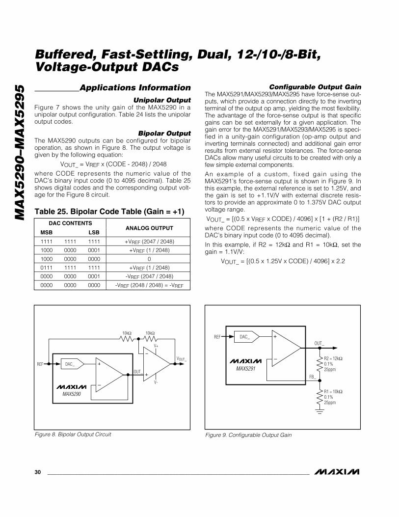
MA
X5
29
0–M
AX
52
95
Buffered, Fast-Settling, Dual, 12-/10-/8-Bit,Voltage-Output DACs
30 ______________________________________________________________________________________
Applications InformationUnipolar Output
Figure 7 shows the unity gain of the MAX5290 in aunipolar output configuration. Table 24 lists the unipolaroutput codes.
Bipolar OutputThe MAX5290 outputs can be configured for bipolaroperation, as shown in Figure 8. The output voltage isgiven by the following equation:
VOUT_ = VREF x (CODE - 2048) / 2048
where CODE represents the numeric value of theDAC’s binary input code (0 to 4095 decimal). Table 25shows digital codes and the corresponding output volt-age for the Figure 8 circuit.
Configurable Output GainThe MAX5291/MAX5293/MAX5295 have force-sense out-puts, which provide a connection directly to the invertingterminal of the output op amp, yielding the most flexibility.The advantage of the force-sense output is that specificgains can be set externally for a given application. Thegain error for the MAX5291/MAX5293/MAX5295 is speci-fied in a unity-gain configuration (op-amp output andinverting terminals connected) and additional gain errorresults from external resistor tolerances. The force-senseDACs allow many useful circuits to be created with only afew simple external components.
An example of a custom, f ixed gain using theMAX5291’s force-sense output is shown in Figure 9. Inthis example, the external reference is set to 1.25V, andthe gain is set to +1.1V/V with external discrete resis-tors to provide an approximate 0 to 1.375V DAC outputvoltage range.
VOUT_ = [(0.5 x VREF x CODE) / 4096] x [1 + (R2 / R1)]
where CODE represents the numeric value of theDAC’s binary input code (0 to 4095 decimal).
In this example, if R2 = 12kΩ and R1 = 10kΩ, set thegain = 1.1V/V:
VOUT_ = [(0.5 x 1.25V x CODE) / 4096] x 2.2
Table 25. Bipolar Code Table (Gain = +1)DAC CONTENTS
MSB LSBANALOG OUTPUT
1111 1111 1111 +VREF (2047 / 2048)
1000 0000 0001 +VREF (1 / 2048)
1000 0000 0000 0
0111 1111 1111 +VREF (1 / 2048)
0000 0000 0001 -VREF (2047 / 2048)
0000 0000 0000 -VREF (2048 / 2048) = -VREF
Figure 8. Bipolar Output Circuit
MAX5290
DAC_REF
OUT_
10kΩ 10kΩ
V+
V-
VOUT_
MAX5291
DAC_REFOUT_
FB_
R2 = 12kΩ0.1%25ppm
R1 = 10kΩ0.1%25ppm
Figure 9. Configurable Output Gain

MA
X5
29
0–M
AX
52
95
Buffered, Fast-Settling, Dual, 12-/10-/8-Bit,Voltage-Output DACs
______________________________________________________________________________________ 31
Power-Supply and Layout ConsiderationsBypass the analog and digital power supplies with a10µF capacitor in parallel with a 0.1µF capacitor to ana-log ground (AGND) and digital ground (DGND) (seeFigure 10). Minimize lead lengths to reduce lead induc-tance. If noise is an issue, use shielding and/or ferritebeads to increase isolation.
Digital and AC transient signals coupling to AGND cre-ate noise at the output. Connect AGND to the highestquality ground available. Use proper grounding tech-
niques, such as a multilayer board with a low-induc-tance ground plane. Wire-wrapped boards and socketsare not recommended. For optimum system perfor-mance, use printed circuit (PC) boards with separateanalog and digital ground planes. Connect the twoground planes together at the low-impedance power-supply source.
Using separate power supplies for AVDD and DVDDimproves noise immunity. Connect AGND and DGND atthe low-impedance power-supply source (see Figure 11).
MAX5290–MAX5295
VREF
10µF* 0.1µF*
REF
SCLK
DIN
PU
UPIO1
UPIO2
CS
DSP
AGND** DGND**
OUTA
FBA
FBB
OUTB
MAX5291/MAX5293/MAX5295
ONLY
10µF0.1µF0.1µF 10µF
DVDDAVDD
DVDDAVDD
*REMOVE BYPASS CAPACITORS ON REF FOR AC-REFERENCE INPUTS.**CONNECT ANALOG AND DIGITAL GROUND PLANES AT THE LOW-IMPEDANCE POWER-SUPPLY SOURCE.
Figure 10. Bypassing Power Supplies and Reference
MAX5290–MAX5295
0.1µF
10µF
AVDD AGND
AVDD AGND
0.1µF
10µF
DVDD DGND
DVDD DGND
DVDD DGND
ANALOG SUPPLY DIGITAL SUPPLY
DIGITALCIRCUITRY
Figure 11. Separate Analog and Digital Power Supplies

MA
X5
29
0–M
AX
52
95
Buffered, Fast-Settling, Dual, 12-/10-/8-Bit,Voltage-Output DACs
32 ______________________________________________________________________________________
Chip InformationTRANSISTOR COUNT: 16,758
PROCESS: BiCMOS
16 15 14 13
9
10
11
12
OUTB
REF
N.C.
OUTA
4
3
2
1
SCLK
CS
DIN
DSP
5 6 7 8
MAX5290MAX5292MAX5294
UPIO
1
UPIO
2
PU N.C.
DVDD
DGND
AGND
AVDD
(4mm x 4mm) THIN QFN
16 15 14 13
9
10
11
12
OUTB
FBB
REF
FBA
4
3
2
1
SCLK
CS
DIN
DSP
5 6 7 8
MAX5291MAX5293MAX5295
UPIO
1
UPIO
2
PU OUTA
DVDD
DGND
AGND
AVDD
(4mm x 4mm) THIN QFN
14
13
12
11
10
9
8
1
2
3
4
5
6
7
UPIO2
PU
OUTA
REFCS
DIN
DSP
UPIO1
TOP VIEW
MAX5290MAX5292MAX5294 OUTB
AVDD
AGNDDGND
DVDD
SCLK
14 TSSOP
16
15
14
13
12
11
10
9
1
2
3
4
5
6
7
8
UPIO2 PU
OUTA
FBA
REF
FBB
OUTB
AVDD
AGND
MAX5291MAX5293MAX5295
16 TSSOP
UPIO1
DSP
SCLK
DIN
CS
DVDD
DGND
Pin Configurations
Selector Guide
PARTOUTPUTBUFFER
CO NFIGUR ATION
R ESO L U TIO N ( B IT S)
INL(LSBsMAX)
MAX5290AEUD Unity Gain 12 ±1
MAX5290BEUD Unity Gain 12 ±4
MAX5290AETE* Unity Gain 12 ±1
MAX5290BETE Unity Gain 12 ±4
MAX5291AEUE Force Sense 12 ±1
MAX5291BEUE Force Sense 12 ±4
MAX5291AETE* Force Sense 12 ±1
MAX5291BETE Force Sense 12 ±4
MAX5292EUD Unity Gain 10 ±1
MAX5292ETE Unity Gain 10 ±1
MAX5293EUE Force Sense 10 ±1
MAX5293ETE Force Sense 10 ±1
MAX5294EUD Unity Gain 8 ±0.5
MAX5294ETE Unity Gain 8 ±0.5
MAX5295EUE Force Sense 8 ±0.5
MAX5295ETE Force Sense 8 ±0.5
*Future product—contact factory for availability. Specificationsare preliminary.

MA
X5
29
0–M
AX
52
95
Buffered, Fast-Settling, Dual, 12-/10-/8-Bit,Voltage-Output DACs
______________________________________________________________________________________ 33
Package Information(The package drawing(s) in this data sheet may not reflect the most current specifications. For the latest package outline informationgo to www.maxim-ic.com/packages.)
TSS
OP
4.40
mm
.EP
S
PACKAGE OUTLINE, TSSOP 4.40mm BODY
21-0066 11
I

MA
X5
29
0–M
AX
52
95
Buffered, Fast-Settling, Dual, 12-/10-/8-Bit,Voltage-Output DACs
34 ______________________________________________________________________________________
Package Information (continued)(The package drawing(s) in this data sheet may not reflect the most current specifications. For the latest package outline informationgo to www.maxim-ic.com/packages.)
24L
QFN
TH
IN.E
PS
PACKAGE OUTLINE,
21-0139 21
F
12, 16, 20, 24, 28L THIN QFN, 4x4x0.8mm

MA
X5
29
0–M
AX
52
95
Buffered, Fast-Settling, Dual, 12-/10-/8-Bit,Voltage-Output DACs
Maxim cannot assume responsibility for use of any circuitry other than circuitry entirely embodied in a Maxim product. No circuit patent licenses areimplied. Maxim reserves the right to change the circuitry and specifications without notice at any time.
Maxim Integrated Products, 120 San Gabriel Drive, Sunnyvale, CA 94086 408-737-7600 ____________________ 35
© 2007 Maxim Integrated Products is a registered trademark of Maxim Integrated Products, Inc.
Package Information (continued)(The package drawing(s) in this data sheet may not reflect the most current specifications. For the latest package outline informationgo to www.maxim-ic.com/packages.)
PACKAGE OUTLINE,
21-0139 22
F
12, 16, 20, 24, 28L THIN QFN, 4x4x0.8mm
Revision HistoryPages changed at Rev 3: 1, 6–9, 33, 34, 35