Buck and Buck-boost configuration. Obsolete Product(s ... · Obsolete Product(s) - Obsolete...
28
® May 2005 1/28 AN1357 - APPLICATION NOTE VIPower: LOW COST POWER SUPPLIES USING VIPer12A IN NON ISOLATED APPLICATIONS INTRODUCTION The industrial field is asking for an increasing number of low power low voltage applications both in isolated and non isolated topology. The main specification is related to the cost of the power converter, which has to be operated in off-line mode. VIPer12A is a low cost monolithic smart power device with an integrated PWM controller that is suitable for such applications. In this paper a detailed analysis of VIPer12A in non isolated applications is performed, exploiting the main features of such a device, in Buck and Buck-boost configuration. 1. OFF-LINE NON ISOLATED CONVERTERS Off-line non isolated topologies convert the mains to regulated DC voltage with no need of any isolation transformer, adjusting the duty cycle of a power switch. The energy is transferred from input to output by a low cost inductor. Two main topologies are used to generate either positive or negative voltage with respect to the common terminal of the input voltage, "step down" (or "buck") and "step-down/up" (or “buck-boost") topology respectively, shown in figure 1. Both topologies use an inductor for energy storage, charged during the turn-on of the power switch. The inductor current waveform defines the mode of operation of the converter, i.e. "continuous" and "discontinuous". In the continuous mode, the inductor current never goes to zero, while in the discontinuous mode such a current is zero for a given time period. A "boundary mode" is also defined, referring to a single zero point of the inductor current. In continuous mode, both converters operate like a transformer with a voltage ratio continuously controlled electronically by means of duty cycle of the switch, D, defined by the ratio between the turn on time, t on , and the switching period T s , according to (1) and (2): When the switch is on, there is a constant voltage across the output inductor (V i -V o ), making the current in it rising linearly at a rate, di/dt, given by (3). V o V i ------ D = buck converter (1) V o V i ------ D 1 D – ------------- = buck-boost converter (2) (3) di dt ---- V i V – o L ----------------- = Rev. 2 Obsolete Product(s) - Obsolete Product(s)
Transcript of Buck and Buck-boost configuration. Obsolete Product(s ... · Obsolete Product(s) - Obsolete...

®
May 2005 1/28
AN1357- APPLICATION NOTE
VIPower: LOW COST POWER SUPPLIESUSING VIPer12A IN NON ISOLATED APPLICATIONS
INTRODUCTION
The industrial field is asking for an increasing number of low power low voltage applications both inisolated and non isolated topology. The main specification is related to the cost of the power converter,which has to be operated in off-line mode. VIPer12A is a low cost monolithic smart power device with anintegrated PWM controller that is suitable for such applications. In this paper a detailed analysis ofVIPer12A in non isolated applications is performed, exploiting the main features of such a device, inBuck and Buck-boost configuration.
1. OFF-LINE NON ISOLATED CONVERTERS
Off-line non isolated topologies convert the mains to regulated DC voltage with no need of any isolationtransformer, adjusting the duty cycle of a power switch. The energy is transferred from input to output bya low cost inductor.
Two main topologies are used to generate either positive or negative voltage with respect to the commonterminal of the input voltage, "step down" (or "buck") and "step-down/up" (or “buck-boost") topologyrespectively, shown in figure 1.
Both topologies use an inductor for energy storage, charged during the turn-on of the power switch. Theinductor current waveform defines the mode of operation of the converter, i.e. "continuous" and"discontinuous". In the continuous mode, the inductor current never goes to zero, while in thediscontinuous mode such a current is zero for a given time period. A "boundary mode" is also defined,referring to a single zero point of the inductor current.
In continuous mode, both converters operate like a transformer with a voltage ratio continuouslycontrolled electronically by means of duty cycle of the switch, D, defined by the ratio between the turn ontime, ton, and the switching period Ts, according to (1) and (2):
When the switch is on, there is a constant voltage across the output inductor (Vi-Vo), making the current
in it rising linearly at a rate, di/dt, given by (3).
Vo
Vi------ D= buck converter (1)
Vo
Vi------ D
1 D–-------------= buck-boost converter (2)
(3)didt-----
Vi V–o
L------------------=
Rev. 2
Obsolete Product(s) -
Obsolete Product(s)

Obsolete Product(s) -
Obsolete Product(s)
2/28
AN1357 - APPLICATION NOTE
As the switch is turned off, the voltage polarity across the inductor immediately reverses trying tomaintain the same current as just before turn off. The diode turns on and clamps the inductor voltage toideally zero. The voltage across L is Vo and its current ramps down linearly at a rate given by (4).
Once the switch turns on again the current in L is diverted from D to the switch S, back biasing the diode.The current in L consists in the switch current when it is on and in the diode current when the switch isoff. The inductor current ramps up and down around the DC value Io with a ripple determined by the Lvalue.
Figure 1: Not isolated power converters
(4)didt-----
Vo
L------–=
Vin C D
L S
Vo
+
_
Io
Vin C
D
L
S
Vo
_
+
Io
Buck configuration
Buck-boost configuration
Obsolete Product(s) -
Obsolete Product(s)
3/28
AN1357 - APPLICATION NOTE
2. FRONT-END RECTIFIER
Single wave or bridge rectifiers could be used for mains rectification. However, if the neutral connection isrequired as ground, the single wave rectifier has to be used. Such a choice determines the minimuminput filter capacitance value.
The rectifier diode is rated for 800V to 1000V of reverse voltage with a 1A current since the power level ofthe considered application is low.
The input bulk capacitor is determined on the basis of the minimum input voltage (that depends on thepower supply specifications, i.e. single or wide range) and on the maximum voltage ripple acceptable inthe input voltage. The rectifier topology, i.e. single wave or full bridge, affects the value of the minimuminput capacitance as well.
A basic consideration has to be taken about the value of the bulk capacitor: although larger values meanlow peak and rms current through the power device and less duty cycle adjustment for regulation, ahigher peak current is drawn from the mains, leading to higher power dissipation in the rectifier andpoorer harmonic behavior.
For low power applications a good compromise is given by the peak-to-peak voltage ripple of 25-30%related to the peak mains voltage. If hold-up capability is required, a larger capacitor is needed.
When a VIPer12A is used as a power switch, a minimum DC input voltage (i.e. 50V) is needed to performa proper start-up operation, thus a higher voltage ripple is allowed. In conclusion, the input bulk capacitoris selected to provide the minimum DC voltage with the lower input AC voltage and the maximum load, inorder to enable VIPer12A control circuit. In such a way, a better power quality performance is obtainedwith no effect on the output voltage regulation, thanks to the high switching frequency and the currentmode control of VIPer12A.
Single wave rectification has been chosen to have the output ground connected to one of the mainslines, as is required in most of non isolated applications.
High-grade electrolytic capacitors with high ripple current capacity and low ESR are usually used with arated voltage of 400Vdc minimum. Referring to Fig. 2, for a given output power Pout and voltage ripple∆V(=Vinpeak - Vinlow), the input capacitor Cin can be calculated using eq. (5).
where "I" is the discharging current, η is the efficiency, Vindc is the DC input voltage and "t" is the timeduring which the capacitor must supply current, given by (6).
The DC input voltage is given by:
(5)Cin
I t⋅∆V--------
Pout
η Vindc⋅---------------------- t⋅
∆V----------------------------= =
(6)t 0.75 T ∆T+⋅ 0.75 T⋅ T2π------+ arc
Vinlow
Vpeak----------------sin⋅= =
(7)Vindc 2 Vinac⋅=

Obsolete Product(s) -
Obsolete Product(s)
4/28
AN1357 - APPLICATION NOTE
Figure 2: DC bus voltage
3. EMI INPUT FILTER
EMI is an issue for SMPS since it is a requirement for CE certification. Some applications may require adecoupling input filter to limit the conducted emission to the mains. The limits established by EU dependon the classification of the power supply, whether industrial or domestic appliances. In order to complywith standard requirements, simple filters can be used in low cost applications, as shown in figure 3,reducing the common-mode emissions. The most common filter topology is the CLC π filter, however forvery noisy high performance circuits the multistage approach is a mandatory solution.
Figure 3: Basic EMI filter
Vpeak
Vmin
Tt
L
C C2
L
C1
C2
L1
C1
L2
Cn
Ln
LC filter CLC π filter
Multistage filter

Obsolete Product(s) -
Obsolete Product(s)
5/28
AN1357 - APPLICATION NOTE
Considering a CLC π filter, a simplified design method is given, based on the corner frequency of the 2ndorder filter, providing a dumping factor ζ higher than 0.5 and a corner frequency much lower than theswitching frequency.
4. OUTPUT INDUCTOR
The design of the output inductor depends on the converter topology as described hereafter for the Buckand Buck-boost converter respectively.
4.1. BUCK CONVERTER
As described in Section 1, the energy is stored in the inductor L during the on-time and then released tothe load during the off-time of the power device. Thus the load is fed both during the on-time and off-timeof the power switch. Since the energy related to the free-wheeling period is negligible compared to theenergy transferred during the on-time -considering only the power transferred to the load during on-time-the inductor value is given by (8) with a good approximation.
where: "Idpeak" is the maximum allowable peak drain current and "fsw" is the switching frequency.
The value of L determines whether the circuit operates in continuous mode or discontinuous mode for agiven output current. Regulators operating in the discontinuous mode are very stable and have a verygood closed loop response; therefore, the discontinuous mode is preferred. However, in discontinuousmode the current stress is higher for a given output power, increasing the ratings of power devices anddecreasing the reliability of the system.
The boundary condition between continuous and discontinuous modes of operation is given by (9), thusto operate in discontinuous mode, the inductor value has to be lower than such a value.
where “R” is the load resistance and “T” is the switching period.
Finally, it is better to avoid the continuous mode because of several reasons:
- Higher switching losses in the switch and free-wheeling diode;
- The inductor size and price would increase- Regulators operating in the discontinuous mode are very stable and have a very good closed loop
response.
4.2. BUCK-BOOST CONVERTER
In the Buck-boost converter the load is supplied only during off-time. Neglecting the power consumptionof VIPer12, the inductor value is still given by (8).
The boundary condition between continuous and discontinuous mode of operation in a buck-boostregulator is given by (10).
The considerations taken about the inductor value in Buck topology apply to Buck-boost topology as well.
(8)L2 Pout⋅
Idpeak2 fsw⋅
----------------------------≅
(9)Lb12--- R T 1 D–( )⋅ ⋅ ⋅=
(10)L12--- R T D 1 D–( )2⋅ ⋅ ⋅ ⋅=
Obsolete Product(s) -
Obsolete Product(s)
6/28
AN1357 - APPLICATION NOTE
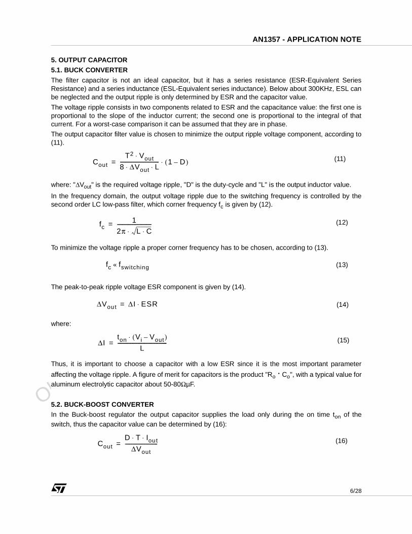
5. OUTPUT CAPACITOR
5.1. BUCK CONVERTER
The filter capacitor is not an ideal capacitor, but it has a series resistance (ESR-Equivalent SeriesResistance) and a series inductance (ESL-Equivalent series inductance). Below about 300KHz, ESL canbe neglected and the output ripple is only determined by ESR and the capacitor value.
The voltage ripple consists in two components related to ESR and the capacitance value: the first one isproportional to the slope of the inductor current; the second one is proportional to the integral of thatcurrent. For a worst-case comparison it can be assumed that they are in phase.
The output capacitor filter value is chosen to minimize the output ripple voltage component, according to(11).
where: "∆Vout" is the required voltage ripple, "D" is the duty-cycle and "L" is the output inductor value.
In the frequency domain, the output voltage ripple due to the switching frequency is controlled by thesecond order LC low-pass filter, which corner frequency fc is given by (12).
To minimize the voltage ripple a proper corner frequency has to be chosen, according to (13).
The peak-to-peak ripple voltage ESR component is given by (14).
where:
Thus, it is important to choose a capacitor with a low ESR since it is the most important parameter
affecting the voltage ripple. A figure of merit for capacitors is the product "Ro · Co", with a typical value foraluminum electrolytic capacitor about 50-80ΩµF.
5.2. BUCK-BOOST CONVERTER
In the Buck-boost regulator the output capacitor supplies the load only during the on time ton of theswitch, thus the capacitor value can be determined by (16):
(11)Cout
T2 Vout⋅8 ∆Vout L⋅ ⋅------------------------------- 1 D–( )⋅=
(12)fc1
2π L C⋅⋅---------------------------=
(13)fc fswitching«
(14)∆Vout ∆ I ESR⋅=
(15)∆Iton Vi Vout–( )⋅
L---------------------------------------=
(16)CoutD T Iout⋅ ⋅
∆Vout--------------------------=

Obsolete Product(s) -
Obsolete Product(s)
7/28
AN1357 - APPLICATION NOTE
As in the Buck regulator, an important parameter affecting the output voltage ripple is the capacitor ESR.Moreover, since the capacitor in the Buck-boost regulator supplies the current during the ton of the powerswitch, the capacitor voltage has a much higher current ripple, making the ESR requirement morestringent.
6. DESIGNING A STEP DOWN CONVERTER USING A VIPer12A
The design of a Buck converter using a VIPer12A is straightforward thanks to the device features, e.g.start-up capability, integrated PWM controller and thermal and overcurrent protection. Moreover thePWM controller is very simple and does not require any external feed-back compensation network.
The circuit schematic is shown in figure 4 for single wave rectification. The power circuit consists in inputrectifier Dr, bulk capacitor for DC bus filtering, Cbulk, power switch VIPer12A, free-wheeling diode D, andoutput LC filter.
6.1. VIPer12A SUPPLY CIRCUIT
The supply voltage for VIPer12A can be easily obtained through the output of the converter by means ofa diode and a capacitor on Vdd pin, D1 and C1 in figure 4. The diode voltage rating depends on the inputvoltage, while the current rating is not an issue. For example, for the European voltage range 185-265Vac a 400V diode can be used.
The capacitor value is chosen according to the start-up time and the short circuit behavior of theconverter. In fact, during a short circuit the Vdd voltage falls down below the minimum required value,enabling the internal high voltage current generator for a new start-up sequence. The charging anddischarging time of the capacitor depends on its value, thus the time period during which the powerswitch is properly supplied changes accordingly. Moreover, if current pulses heat considerably thedevice, the over temperature protection shuts off the circuit.
Typical values range from 300nF to 10uF, while the voltage rating is at least 40-50V.
6.2. VIPer12A REGULATION CIRCUIT
The output voltage regulation circuit simply consists of a zener diode Dz across FB and Vdd pins, asshown in figure 4. To perform a better regulation, a filter capacitor C2 can be connected across FB and Spins. The C2 value is in the order of some tens of nF.
If the output voltage is lower than 16V the circuit has to be slightly modified in order to allow the start upof VIPer12A. In such a case the regulation circuit has to be decoupled from the supply circuit, using aseparate diode and capacitor to supply the zener diode on FB pin, D2 and C3 in figure 5. The diode D2 isa low voltage diode, e.g. 1N4148, and allows the voltage on Vdd to reach the start-up value. Since D2 andC3 realize a peak detector of the output voltage, C3 value influences the precision of the regulationcircuit. If high precision is not an issue it can be as low as 100nF. To prevent disturbance resulting inpossible output overvoltage or incorrect start-up, a zener diode Do is connected across the output. Thevalue must be 2 or 3 volts higher than the output voltage. For further details please refer to the A.N. 1317(NON ISOLATED POWER SUPPLIES IN BUCK AND INVERTER CONFIGURATION USING VIPer20DEVICE -A. Bailly - S. Luciano).

Obsolete Product(s) -
Obsolete Product(s)
8/28
AN1357 - APPLICATION NOTE
Figure 4: Buck converter with Vout>16V
Figure 5: Buck converter with Vout<16V
D C Vin(ac) Vout(dc)
Vdd
Dz
GND
+
_
C1
L D S VIPer 12
C2 FB
D1
Dr
Cbulk Do
D C Vin(ac) Vout(dc)
Vdd
Dz
GND
+
_
C1
L D S VIPer 12 C2
FB
C3
Dr
D2 D1
Cbulk
Obsolete Product(s) -
Obsolete Product(s)
9/28
AN1357 - APPLICATION NOTE
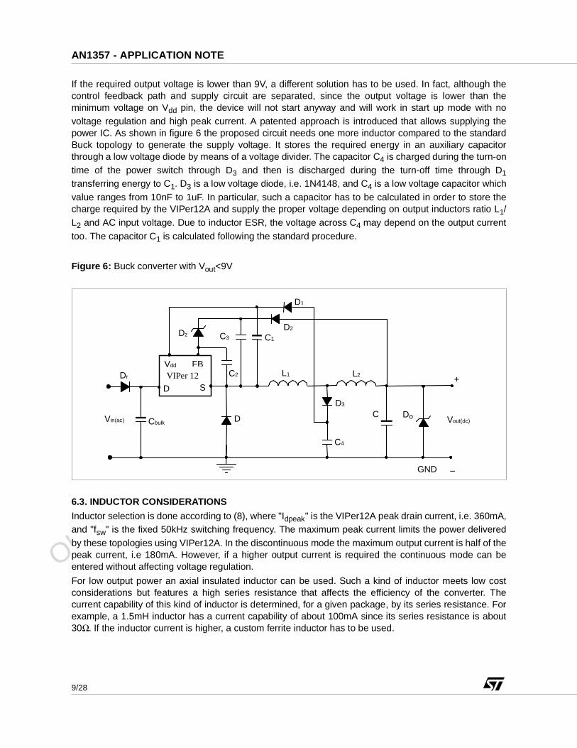
If the required output voltage is lower than 9V, a different solution has to be used. In fact, although thecontrol feedback path and supply circuit are separated, since the output voltage is lower than theminimum voltage on Vdd pin, the device will not start anyway and will work in start up mode with novoltage regulation and high peak current. A patented approach is introduced that allows supplying thepower IC. As shown in figure 6 the proposed circuit needs one more inductor compared to the standardBuck topology to generate the supply voltage. It stores the required energy in an auxiliary capacitorthrough a low voltage diode by means of a voltage divider. The capacitor C4 is charged during the turn-ontime of the power switch through D3 and then is discharged during the turn-off time through D1
transferring energy to C1. D3 is a low voltage diode, i.e. 1N4148, and C4 is a low voltage capacitor whichvalue ranges from 10nF to 1uF. In particular, such a capacitor has to be calculated in order to store thecharge required by the VIPer12A and supply the proper voltage depending on output inductors ratio L1/L2 and AC input voltage. Due to inductor ESR, the voltage across C4 may depend on the output currenttoo. The capacitor C1 is calculated following the standard procedure.
Figure 6: Buck converter with Vout<9V
6.3. INDUCTOR CONSIDERATIONS
Inductor selection is done according to (8), where "Idpeak" is the VIPer12A peak drain current, i.e. 360mA,and "fsw" is the fixed 50kHz switching frequency. The maximum peak current limits the power deliveredby these topologies using VIPer12A. In the discontinuous mode the maximum output current is half of thepeak current, i.e 180mA. However, if a higher output current is required the continuous mode can beentered without affecting voltage regulation.
For low output power an axial insulated inductor can be used. Such a kind of inductor meets low costconsiderations but features a high series resistance that affects the efficiency of the converter. Thecurrent capability of this kind of inductor is determined, for a given package, by its series resistance. Forexample, a 1.5mH inductor has a current capability of about 100mA since its series resistance is about30Ω. If the inductor current is higher, a custom ferrite inductor has to be used.
D C Vin(ac)
Vdd
Dz C1
L1 D S VIPer 12 C2
FB
C3
L2
Cbulk
Dr
D1
D2
D3
C4
Vout(dc)
GND
+
_
Do

Obsolete Product(s) -
Obsolete Product(s)
10/28
AN1357 - APPLICATION NOTE
6.4. APPLICATION EXAMPLES
The first application example is a 16V-100mA off-line power supply. Converter specifications are given intable 1. The schematic of the circuit is shown in figure 7.
A single wave rectification is performed in order to have the ground connected to the neutral of themains. In this case to improve the reverse voltage robustness a series connection of two high voltagediodes can be used for rectification. The bulk capacitor can be selected according to table 2, that lists theminimum input capacitor for a given input voltage range and output current. Such a minimum valueresults in DC voltage ripple that is beneficial in terms of power quality and efficiency. A higher voltageripple means that the capacitor draws current for a longer period reducing the current peak and thusreducing the low frequency harmonic content of the input current. On the other hand, for a givenminimum duty cycle the current in the switch is lower because of a lower input voltage, reducing powerlosses and thus increasing the efficiency. Of course, in the case of a bridge rectifier the values can beconsiderably reduced. As shown in figure 7, the input bulk capacitor is split in two capacitors and aninductor is inserted in between, realizing an EMI filter as described in Section 3. The components list isgiven in table 3.
Table 1: Buck converter specifications
Table 2: Input capacitor selection table
Figure 7: Application example: 16V-100mA power supply
AC input voltage 185 - 265VacOutput power 1.5WOutput voltage +16V
Input Capacitor
Cin
Maximum Output current90Vac Minimum input voltage
(Wide range)
180Vac Minimum input voltage
(Single range)1µF 15mA 80mA
2.2µF 40mA 100mA3.3µF 60mA 120mA4.7µF 80mA 150mA
D C Vac
+16V Vdd
Dz C1
L D S VIPer 12
C2 FB
D1
Dr
Cin1
Rf Lf
185-265V Cin2 Vout(dc)
GND _
Do

Obsolete Product(s) -
Obsolete Product(s)
11/28
AN1357 - APPLICATION NOTE
Table 3: Components list
The proposed power supply can be successfully applied in microcontroller-based low power motor drivesystems. Such an application requires two regulated output voltage: 15V for power switch gate driver and5V for microcontroller. In figure 8 the circuit schematic is shown, using a 5V linear regulator with reset forproper system operation. This circuit assures good performance in terms of size and performances atvery low cost.
Figure 8: Application example: double output converter for microcontroller supply
REFERENCE VALUE PART NUMBER
Rf 10Ω / 1/2WCin1 1µF / 400V ElectrolyticCin2 1µF / 400V ElectrolyticC1 10µF / 25V ElectrolyticC2 22nF / 25V CeramicCout 10µF / 25V ElectrolyticDo 18V Zener BZX55C18VD1 1A - 600V STTA106D2 1A - 600V STTA106Dr 1A - 1000V 1N4007Dz 15 V ZenerL 1.8mHLf 680µHIC1 VIPer12ADIP
D C VAC
+16V Vdd
Dz C1
L D S VIPer 12
C2 FB
D1
Dr
Cin2
Rf
L4949
Co
Reset
IN OUT +5V
Cin1
Lf
Vout(dc)
GND _
Do

Obsolete Product(s) -
Obsolete Product(s)
12/28
AN1357 - APPLICATION NOTE
6.5. LAYOUT CONSIDERATIONS
The circuit layout is shown in figure 9 for all the proposed configurations, with single and full waverectification. The size of the board is 3.5x4 mm and could be further reduced if SMD components wereused. However, in such a case the board is more expensive and does not fit the low cost requirements.
The design of a PCB layout is not an easy task. Component placing and trace routing strongly affect thefunctionality and EMI behavior of the board. Moreover, adequate clearance is required for insulationissues between high and low voltage circuits.
In doing so, power traces have to be as short and wide as possible, minimizing resistive and inductiveeffects in order to improve efficiency and reduce the EMI noise.
Figure 9: PCB Layout (not in scale)
6.6. EXPERIMENTAL RESULTS
Typical waveforms of the 16V power supply are shown in figure 10 and figure 11, with Iout=50mA andIout=100mA respectively. In particular, as shown in figure 11, the converter is in boundary condition forIout=100mA. In figure 12 the output voltage and the source voltage in open load condition are shown. Insuch a case the VIPer12A operates in burst mode, decreasing the effective switching frequency andreducing the power consumption to less the 100mW.

Obsolete Product(s) -
Obsolete Product(s)
13/28
AN1357 - APPLICATION NOTE
Figure 10: Buck converter with Vout=16V: normal operation with Iout=50mA
Figure 11: Buck converter with Vout=16V: normal operation with Iout=100mA
C1 – Iout
C2 - Vsource
C4 - Vout
C1 – Iout
C2 – Vsource
C3 – IL
C4 - Vdd

Obsolete Product(s) -
Obsolete Product(s)
14/28
AN1357 - APPLICATION NOTE
Figure 12: Buck converter with Vout=16V: open load condition
Figure 13: Buck converter with Vout=16V: short circuit condition
C2 – Vsource C4 - Vout
Open – Load Condition
Short-circuit condition
C1 – Iout C2 – Vsource C4 - Vdd

Obsolete Product(s) -
Obsolete Product(s)
15/28
AN1357 - APPLICATION NOTE
In short circuit condition VIPer12A limits the short circuit current thanks to three main features: start-upsequence due to low Vdd voltage, current limit function and thermal shut down. This way the powerdissipation is strongly reduced and the converter is safely protected. It is worth noting that the inputresistor and the series resistance of the output inductor also limit the short circuit current . A typical shortcircuit operation is shown in figure 13.
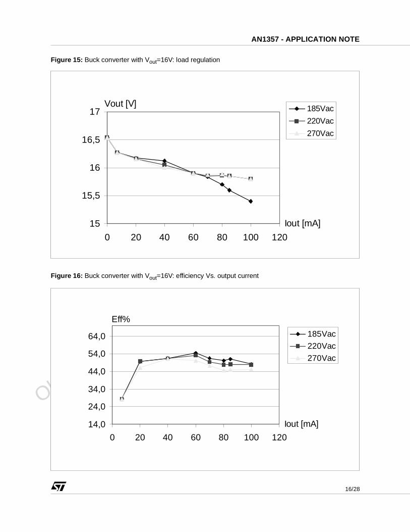
The performance of the circuit has been evaluated and fully characterized, as shown from figure 14 tofigure 19. In particular, the circuit features a good line and load regulation, as shown in figure 14 andfigure 15 respectively. The worst regulation at low input voltage and high output current is basicallyrelated to the value of the input capacitors, a trade off between performance, size and cost.
The efficiency of the power supply is higher than 50%, as shown in figure 16 and figure 17 as a functionof output current and input voltage respectively, and is considerably affected by the parasitic resistance ofthe components. High quality components could be used to improve the efficiency, but a trade offbetween cost and performance has to be done for such a low cost application.
Figure 14: Buck converter with Vout=16V: line regulation
The EMI behavior of VIPer12A-based power supply is shown in figure 18 and figure 19. Conductedemission measurements have been performed according to the standard EN55022 using a 50Ω LISN(Line Impedance Stabilization Network), with a peak detector, in the frequency range 0.15-30 MHz. Asshown in figure 18, the power supply features low conducted emissions even with no input EMI filter,taking into account that the limit lines are related to Quasi-peak and Average detector and theexperimental traces have been measured with a peak detector. In figure 19 the effect of the input EMI filteron the conducted emissions is shown.
15
15.5
16
16.5
17
150 200 250 300Vin [V]
Vout [V]
7mA
20mA
40mA
60mA
70mA
80mA
85mA
100mA
Obsolete Product(s) -
Obsolete Product(s)
16/28
AN1357 - APPLICATION NOTE
Figure 15: Buck converter with Vout=16V: load regulation
Figure 16: Buck converter with Vout=16V: efficiency Vs. output current
15
15,5
16
16,5
17
0 20 40 60 80 100 120
Iout [mA]
Vout [V] 185Vac
220Vac
270Vac
14,0
24,0
34,0
44,0
54,0
64,0
0 20 40 60 80 100 120
Iout [mA]
Eff%
185Vac
220Vac
270Vac

Obsolete Product(s) -
Obsolete Product(s)
17/28
AN1357 - APPLICATION NOTE
Figure 17: Buck converter with Vout=16V: efficiency Vs. input ac voltage
Figure 18: Buck converter with Vout =16V: EMI behavior with no input filter
20,0
25,030,0
35,0
40,045,0
50,0
55,060,0
150 200 250 300Vin [V]
Eff%7mA
20mA40mA
60mA70mA
80mA85mA
100mA
A: EN 55022: Class A Conducted, Quasi-PeakB: EN 55022: Class A, Average
Iload=100mA
no load
0
10
20
30
40
50
60
70
80
90
100
1 10
dBuV (Start = 0.15, Stop = 30.00) MHz
Noise
A
B

Obsolete Product(s) -
Obsolete Product(s)
18/28
AN1357 - APPLICATION NOTE
Figure 19: Buck converter with Vout =16V: EMI behavior with EMI input filter
6.7. 5V-60mA BUCK CONVERTER
The second application example is related to a 5V-60mA power supply. The schematic of the circuit isshown in figure 20. In this application a suitable circuit has been developed to properly supply the devicesince the output voltage is lower than the minimum Vdd voltage, i.e. 8V. Such a circuit consists instandard low cost components L2, D3 and C4, as described in table 4. The selection of L2 value dependson the input ac voltage range, since the voltage provided to Vdd is function of L1/L2 ratio. For theEuropean voltage range, i.e. 185-265V, a ratio of 3-4 is the right choice. If low cost inductors with highseries resistance were used, the voltage across C4 would be influenced by the output current as well.The C4 value is about 80-100nF with a voltage rating given by the inductor ratio. Basically, C4 has tostore the energy needed by the VIPer12A and then transfer it to C1.
Noise
no load
Iload=100mA
0 10 20 30 40 50 60 70 80 90
100
1 10
dBuV (Start = 0.15, Stop = 30.00) MHz
A
B
A: EN 55022: Class A Conducted, Quasi-PeakB: EN 55022: Class A, Average
Obsolete Product(s) -
Obsolete Product(s)
19/28
AN1357 - APPLICATION NOTE
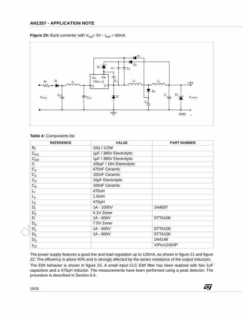
Figure 20: Buck converter with Vout= 5V - Iout = 60mA
Table 4: Components list
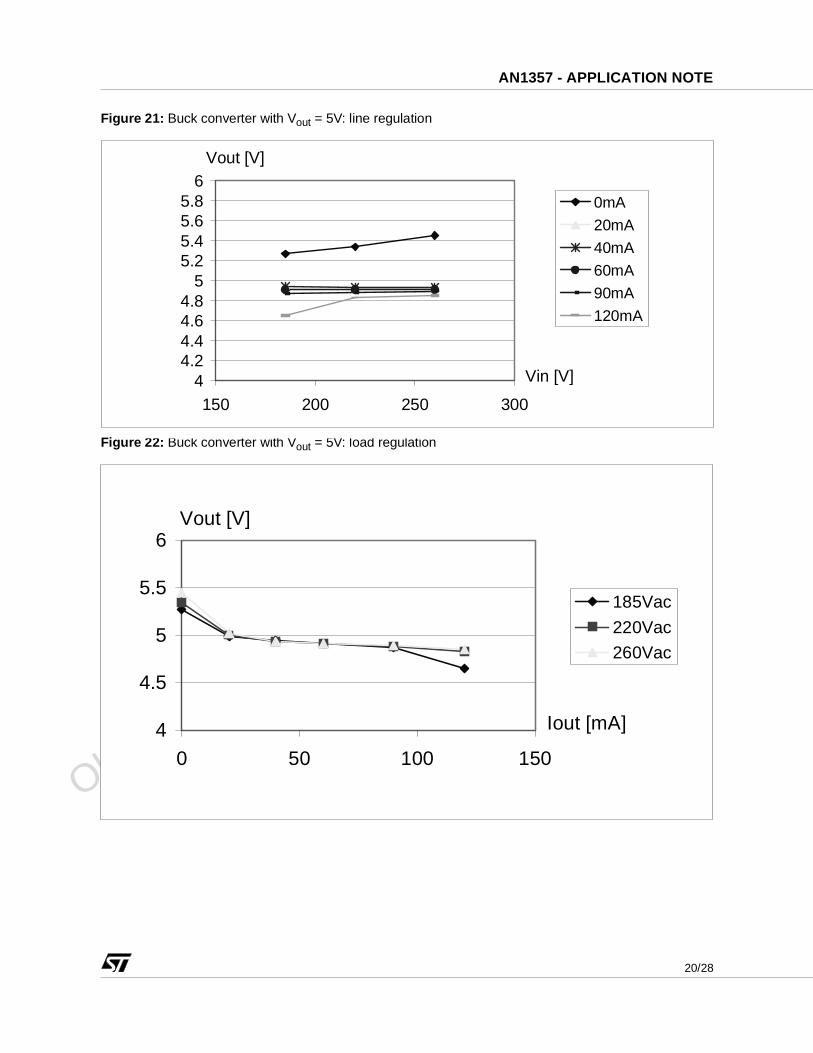
The power supply features a good line and load regulation up to 120mA, as shown in figure 21 and figure22. The efficiency is about 40% and is strongly affected by the series resistance of the output inductors.
The EMI behavior is shown in figure 23. A small input CLC EMI filter has been realized with two 1uFcapacitors and a 470µH inductor. The measurements have been performed using a peak detector. Theprocedure is described in Section 6.6.
REFERENCE VALUE PART NUMBER
Rf 10Ω / 1/2WCin1 1µF / 385V ElectrolyticCin2 1µF / 385V ElectrolyticC 100µF / 16V ElectrolyticC1 470nF CeramicC2 100nF CeramicC3 10µF ElectrolyticC4 100nF CeramicLf 470uHL1 1.5mHL2 470µHDr 1A - 1000V 1N4007Dz 5.1V ZenerD 1A - 600V STTA106Do 7.5V ZenerD1 1A - 600V STTA106D2 1A - 600V STTA106D3 1N4148IC1 VIPer12ADIP
D C Vin(ac)
Vdd
Dz C1
L1 D S VIPer 12 C2
FB
C3
L2
Cin2
Dr
D1
D2
C4
Cin1 D3
Rf Lf +5V
Vout(dc)
GND _
Do
Obsolete Product(s) -
Obsolete Product(s)
20/28
AN1357 - APPLICATION NOTE
Figure 21: Buck converter with Vout = 5V: line regulation
Figure 22: Buck converter with Vout = 5V: load regulation
44.24.44.64.8
55.25.45.65.8
6
150 200 250 300
Vin [V]
Vout [V]
0mA
20mA
40mA
60mA
90mA
120mA
4
4.5
5
5.5
6
0 50 100 150
Iout [mA]
Vout [V]
185Vac
220Vac
260Vac

Obsolete Product(s) -
Obsolete Product(s)
21/28
AN1357 - APPLICATION NOTE
Figure 23: Buck converter with Vout = 5V: EMI behavior with CLC input filter
7. DESIGNING A BUCK-BOOST CONVERTER USING A VIPer12A
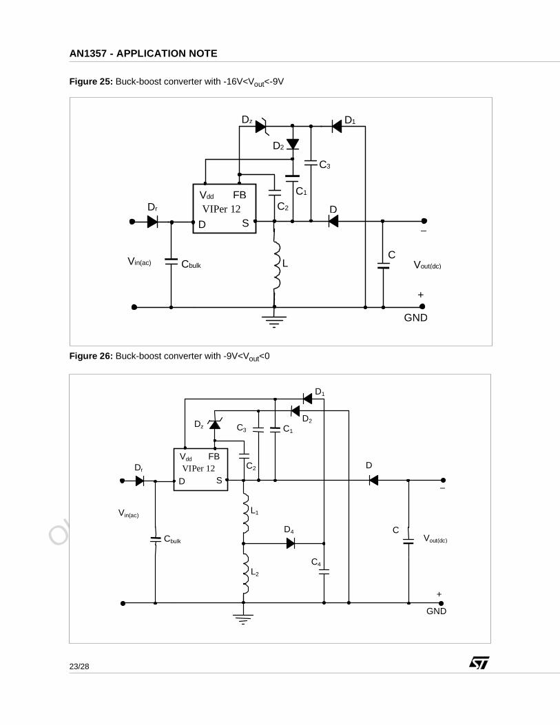
The design of a Buck-boost converter for negative output voltage is as easy as described in Section 6 forthe Buck topology. The circuit schematic with output voltage lower than (-16V) is shown in figure 24 forsingle wave rectification. In figure 25 and figure 26 the circuit schematics for -16V< Vout < -9V and -9V <Vout are respectively shown.
7.1 VIPer12A SUPPLY CIRCUIT
In this topology the supply circuit for VIPer12A is implemented connecting a diode D1 between theground of the converter and a capacitor C1 on Vdd pin, as shown in figure 24. In such a way the voltageon Vdd is positive and the VIPer12A can be properly fed. In particular, the capacitor C1 receives energyduring the off time toff and supplies the VIPer12A during the on time ton. The diode selection is based onthe input voltage while the capacitor value is determined by the start-up time, as discussed in section 6.1.
7.2 VIPer12A REGULATION CIRCUIT
The output voltage regulation circuit consists of a zener diode across FB and Vdd pins, as described inSection 6.2 for Buck topology. If the required output voltage is higher than (-8V), i.e. (-5V), a differentsolution has to be used, as shown in figure 26. The diode D4 is a low voltage diode, e.g. 1N4148, and thevalue of C4 is about 100nF in order to store the energy required by the VIPer12A. The capacitor C1 iscalculated following the standard procedure. The capacitor C2 is connected between FB and S pins toimprove the regulation.
EN 55022; Class A Conducted, Quasi-Peak
EN 55022; Class A Conducted, Average
Noise
0 10 20 30 40 50 60 70 80 90
100
1 10
dBuV (Start = 0.15, Stop = 30.00) MHz

Obsolete Product(s) -
Obsolete Product(s)
22/28
AN1357 - APPLICATION NOTE
7.3 INDUCTOR CONSIDERATIONS
The considerations done about the inductor value in Buck topology apply to Buck-boost topology as well.
7.4. APPLICATION EXAMPLE
The considered circuit provides regulated 16V negative voltage output using the buck-boost non isolatedconfiguration. Converter specifications are listed in table 5. Table 6 shows the components list of thepower supply shown in figure 24.
As shown in figure 27 and figure 28, the circuit performs good voltage and line regulation. The efficiencyof the circuit is as higher as more than 60%, as shown in figure 29 and figure 30. This power supplyfeatures higher efficiency than the positive counterpart only because of the lower series resistance of theinductor.
Table 5: Buck-boost converter specifications
Figure 24: Buck-boost converter with Vout< -16V
AC input voltage 185 - 265VACOutput power 3.5WDC Output voltage -16V
D
C Vin(ac) Vout(dc)
Vdd
Dz
GND +
_
C1
L
D S VIPer 12
C2 FB
D1
Dr
Cbulk
Obsolete Product(s) -
Obsolete Product(s)
23/28
AN1357 - APPLICATION NOTE
Figure 25: Buck-boost converter with -16V<Vout<-9V
Figure 26: Buck-boost converter with -9V<Vout<0
D
C Vin(ac)
Vout(dc)
Vdd
Dz
GND +
_
C1
L1
D S VIPer 12 C2
FB
C3
L2
Cbulk
Dr
D1
D2
D4
C4
D
C Vin(ac) Vout(dc)
Vdd
Dz
GND
+
_
C1
L
D S VIPer 12 C2
FB
C3
Dr
Cbulk
D1
D2

Obsolete Product(s) -
Obsolete Product(s)
24/28
AN1357 - APPLICATION NOTE
Table 6: Components list
Figure 27: Buck-boost converter with Vout= -16V: line regulation
REFERENCE VALUE PART NUMBER
R1 2KΩ / 1/4WC1 10µF / 25V ElectrolyticC2 22nF / 25V CeramicCbulk 4.7µF / 400V ElectrolyticC 100µF / 25V ElectrolyticD1 1A - 600V STTA106D2 1A - 600V STTA106Dr 1A -1000V 1N4007Dz 15V ZenerL 1.6mHIC1 VIPer12ADIP
negative output
14
14.5
15
15.5
16
16.5
17
150 200 250 300
Vin [V]
Vout [V]
0mA40mA80mA100mA150mA200mA230mA

Obsolete Product(s) -
Obsolete Product(s)
25/28
AN1357 - APPLICATION NOTE
Figure 28: Buck-boost converter with Vout= -16V: load regulation
Figure 29: Buck-boost converter with Vout= -16V: efficiency Vs. output current
negative output
14
14.5
15
15.5
16
16.5
17
0 50 100 150 200 250
Iout [mA]
Vout [V]
185Vac220Vac260Vac
negative output
30.035.040.045.050.055.060.065.070.0
0 40 80 120 160 200 240
Iout [mA]
Eff%185Vac220Vac260Vac

Obsolete Product(s) -
Obsolete Product(s)
26/28
AN1357 - APPLICATION NOTE
Figure 30: Buck-boost converter with Vout= -16V: efficiency Vs input voltage
CONCLUSION
Several configurations have been introduced in Buck and Buck-boost configuration exploiting the mainfeatures of VIPer12A so as to realize low power and low cost non isolated power supplies for industrialapplications. The inherent advantages of high frequency switched mode power conversion, allow off-linepower supplies to operate with high efficiency and reduced cost and size. Viper12A, integrating a PWMcontroller and a power device in a single chip, maximizes such advantages in the power range up to fewwatts.
For further information about VIPer12A please consult the official datasheet on the VIPower web page:http://www.st.com/vipower.
negative output
35.0
40.0
45.0
50.0
55.0
60.0
65.0
70.0
150 200 250 300
Vin [V]
Eff%
20mA40mA60mA100mA150mA250mA

Obsolete Product(s) -
Obsolete Product(s)
27/28
AN1357 - APPLICATION NOTE
REVISION HISTORY
Table 6. Revision History
Date Revision Description of Changes
May-2001 1 First Release
31-May-2005 2 Text modified

Obsolete Product(s) -
Obsolete Product(s)
28/28
AN1357 - APPLICATION NOTE
Information furnished is believed to be accurate and reliable. However, STMicroelectronics assumes no responsibility for the consequencesof use of such information nor for any infringement of patents or other rights of third parties which may result from its use. No license is grantedby implication or otherwise under any patent or patent rights of STMicroelectronics. Specifications mentioned in this publication are subjectto change without notice. This publication supersedes and replaces all information previously supplied. STMicroelectronics products are notauthorized for use as critical components in life support devices or systems without express written approval of STMicroelectronics.
The ST logo is a registered trademark of STMicroelectronics.
All other names are the property of their respective owners
© 2005 STMicroelectronics - All rights reserved
STMicroelectronics group of companies
Australia - Belgium - Brazil - Canada - China - Czech Republic - Finland - France - Germany - Hong Kong - India - Israel - Italy - Japan - Malaysia - Malta - Morocco - Singapore - Spain - Sweden - Switzerland - United Kingdom - United States of America
www.st.com