BTI 2012 Malaysia ( Bertelsmann Stiftung’s Transformation Index (BTI) 2012 for MALAYSIA

BTI inSRAMMitigation for BTI ageing in SRAM memo-ries
L.J. Hamburger
Tech
nisc
heUn
iversiteitDe
lft


BTI in SRAMMitigation for BTI ageing in SRAM memories
by
L.J. Hamburgerto obtain the degree of Master of Science
at the Delft University of Technology,to be defended publicly on Wednesday November 25, 2020 at 12:00.
Student number: 4292936Project duration: September 2, 2019 – November 25, 2020Thesis committee: Prof. Said Hamdioui, TU Delft, supervisor
Dr.ir Rene Van Leuken, TU DelftDr.ir Mottaqiallah Taouil, TU DelftIr Daniel Kraak, TU Delft
An electronic version of this thesis is available at http://repository.tudelft.nl/.

Abstract
The aggressive downscaling of the transistor has led to gigantic improvements in the performance and func-tionality of electronics. As a result, electronics have become a significant part in our daily lives whose absencewould be difficult to imagine. Our cars, for example, now consist of many sensors and small computers eachcontrolling certain parts of the car. A downside of the aggressive downscaling of transistor sizes is that it nega-tively impacts the reliability and accelerated ageing, and thus a reduced lifetime, of electronics. Nevertheless,to ensure the reliable operation of electronics, it has therefore become essential to assess the reliability ofany of its embedded components accurately. Conventionally, to combat ageing, designers use guardbandeddesign; adding design margins. These margins, however, lead to a penalty in area, power, and speed. Al-ternatively, one may investigate mitigation schemes that aim at reducing the impact of ageing to extend thereliability and lifetime. These mitigation schemes may lead to a higher performance compared with the con-ventional guardbanded design. This work focuses on an ageing mitigation scheme for SRAMs. SRAMs typi-cally have the highest contribution to the total area of integrated circuits. Therefore, they are highly optimised(i.e. their integration density is the lowest). This also makes them one of the most susceptible componentsto ageing. Hence, providing appropriate ageing mitigation schemes for SRAMs is essential for the overallreliability of ICs.
Whereas prior work has mainly investigated hardware-based ageing mitigation schemes for SRAMs, thisthesis investigates the possibility of mitigating the ageing through software. The advantages of this approachinclude that it does not require circuit changes (and, thus applicable to existing circuits) and it comes at zeroarea overhead. This study’s proposed software-based scheme is based on periodically running a mitigationroutine. This mitigation scheme flips the contents of the memory cells to put the transistors into relaxationfrom BTI stress, the most crucial ageing mechanism in deeply scaled CMOS process. The results show that thesoftware-based scheme can significantly reduce the ageing of the memory at a low overhead. For example,the degradation of the hold SNM metric of the memory cell is reduced with up to 40% at a runtime overhead ofonly 1.4%. Moreover, the scheme also mitigates the ageing of other components of the memory. For example,the degradation of the offset voltage of the sense amplifier is reduced by nearly 50%. This thesis shows that itis possible to use software to mitigate the ageing effects in the memory components and it is worthwhile toconsider implementing it.
iii


Preface
Thank you to all who have been during my thesis or study.To my closest friends for supporting me and always being there to proofread parts of my thesis, even it
meant reading more mistakes than correct words.To my colleges at Insyde and fellow master students, Profs, PhD’ers, and employers for supporting me and
having fun events.Next to this, I would like to thank the IRIS, many hours have been made to program the software and
support the different organisation hosting a rowing competition. It is always great fun to travel to the compe-tition itself and feel the vibe there and make the rowers happy with a well-organised event. The competitionsranged in size from a few hundred people participating in events where thousands of people would partici-pate, and even more people checking the results.
L.J. HamburgerDelft, November 2020
v

Contents
Abstract iii
List of Figures ix
List of Tables xi
Glossary xiii
Acronyms xv
1 Introduction 11.1 Motivation . . . . . . . . . . . . . . . . . . . . . . . . . . . . . . . . . . . . . . . . . . . . 11.2 State of the Art . . . . . . . . . . . . . . . . . . . . . . . . . . . . . . . . . . . . . . . . . . 2
1.2.1 Ageing mitigation schemes . . . . . . . . . . . . . . . . . . . . . . . . . . . . . . . . 21.2.2 Sensing . . . . . . . . . . . . . . . . . . . . . . . . . . . . . . . . . . . . . . . . . . 41.2.3 State-of-the-art limitations . . . . . . . . . . . . . . . . . . . . . . . . . . . . . . . . 5
1.3 Contributions . . . . . . . . . . . . . . . . . . . . . . . . . . . . . . . . . . . . . . . . . . . 51.4 Outline . . . . . . . . . . . . . . . . . . . . . . . . . . . . . . . . . . . . . . . . . . . . . . 6
2 SRAM Design 72.1 Computer memory . . . . . . . . . . . . . . . . . . . . . . . . . . . . . . . . . . . . . . . . 72.2 SRAM organization . . . . . . . . . . . . . . . . . . . . . . . . . . . . . . . . . . . . . . . . 8
2.2.1 Memory cell array . . . . . . . . . . . . . . . . . . . . . . . . . . . . . . . . . . . . . 92.2.2 Address decoder . . . . . . . . . . . . . . . . . . . . . . . . . . . . . . . . . . . . . . 92.2.3 Sense amplifier . . . . . . . . . . . . . . . . . . . . . . . . . . . . . . . . . . . . . . 92.2.4 Write driver . . . . . . . . . . . . . . . . . . . . . . . . . . . . . . . . . . . . . . . . 102.2.5 Timing circuit . . . . . . . . . . . . . . . . . . . . . . . . . . . . . . . . . . . . . . . 10
2.3 SRAM metrics . . . . . . . . . . . . . . . . . . . . . . . . . . . . . . . . . . . . . . . . . . . 102.3.1 Memory cell . . . . . . . . . . . . . . . . . . . . . . . . . . . . . . . . . . . . . . . . 132.3.2 Sense amplifier . . . . . . . . . . . . . . . . . . . . . . . . . . . . . . . . . . . . . . 13
3 Overview on SRAM Reliability Modelling and Mitigation 173.1 Failure mechanisms of transistors. . . . . . . . . . . . . . . . . . . . . . . . . . . . . . . . . 17
3.1.1 Bias Temperature Instability . . . . . . . . . . . . . . . . . . . . . . . . . . . . . . . . 173.1.2 Random Telegraph Noise . . . . . . . . . . . . . . . . . . . . . . . . . . . . . . . . . 193.1.3 Time-Dependent Dielectric Breakdown . . . . . . . . . . . . . . . . . . . . . . . . . . 193.1.4 Hot Carrier Injection . . . . . . . . . . . . . . . . . . . . . . . . . . . . . . . . . . . . 193.1.5 Electromigration . . . . . . . . . . . . . . . . . . . . . . . . . . . . . . . . . . . . . . 19
3.2 SRAM Reliability Modelling . . . . . . . . . . . . . . . . . . . . . . . . . . . . . . . . . . . . 203.2.1 Memory cell array . . . . . . . . . . . . . . . . . . . . . . . . . . . . . . . . . . . . . 203.2.2 Peripheral circuitry and partial or complete memory system . . . . . . . . . . . . . . . 20
3.3 SRAM Mitigation . . . . . . . . . . . . . . . . . . . . . . . . . . . . . . . . . . . . . . . . . 213.3.1 Mitigation at design-time . . . . . . . . . . . . . . . . . . . . . . . . . . . . . . . . . 213.3.2 Better-than-worst-case design strategy . . . . . . . . . . . . . . . . . . . . . . . . . . 213.3.3 Mitigation during run-time . . . . . . . . . . . . . . . . . . . . . . . . . . . . . . . . 21
4 Mitigation Methodology 234.1 Static stress . . . . . . . . . . . . . . . . . . . . . . . . . . . . . . . . . . . . . . . . . . . . 234.2 Memory access modelling . . . . . . . . . . . . . . . . . . . . . . . . . . . . . . . . . . . . 23
4.2.1 Concluding . . . . . . . . . . . . . . . . . . . . . . . . . . . . . . . . . . . . . . . . 254.3 Concept of the mitigation scheme . . . . . . . . . . . . . . . . . . . . . . . . . . . . . . . . 25
4.3.1 BTI effect in a transistor and mitigation potential . . . . . . . . . . . . . . . . . . . . . 25
vii

viii Contents
4.4 Software mitigations . . . . . . . . . . . . . . . . . . . . . . . . . . . . . . . . . . . . . . . 274.4.1 Multiple cell mitigations . . . . . . . . . . . . . . . . . . . . . . . . . . . . . . . . . . 27
4.5 Hardware mitigations . . . . . . . . . . . . . . . . . . . . . . . . . . . . . . . . . . . . . . . 284.5.1 Cyclic flipping . . . . . . . . . . . . . . . . . . . . . . . . . . . . . . . . . . . . . . . 29
5 Experimental Results 315.1 Simulation methodology . . . . . . . . . . . . . . . . . . . . . . . . . . . . . . . . . . . . . 31
5.1.1 High-level overview . . . . . . . . . . . . . . . . . . . . . . . . . . . . . . . . . . . . 315.1.2 Low-level simulation. . . . . . . . . . . . . . . . . . . . . . . . . . . . . . . . . . . . 32
5.2 Performed experiments . . . . . . . . . . . . . . . . . . . . . . . . . . . . . . . . . . . . . . 325.2.1 Setup. . . . . . . . . . . . . . . . . . . . . . . . . . . . . . . . . . . . . . . . . . . . 325.2.2 BTI effect in the cell . . . . . . . . . . . . . . . . . . . . . . . . . . . . . . . . . . . . 345.2.3 BTI effect in the sense amplifier . . . . . . . . . . . . . . . . . . . . . . . . . . . . . . 34
5.3 Software Mitigation Results . . . . . . . . . . . . . . . . . . . . . . . . . . . . . . . . . . . . 355.3.1 Cell performance . . . . . . . . . . . . . . . . . . . . . . . . . . . . . . . . . . . . . 355.3.2 Sense amplifier . . . . . . . . . . . . . . . . . . . . . . . . . . . . . . . . . . . . . . 37
5.4 Hardware Mitigation Results . . . . . . . . . . . . . . . . . . . . . . . . . . . . . . . . . . . 405.4.1 Cell performance . . . . . . . . . . . . . . . . . . . . . . . . . . . . . . . . . . . . . 405.4.2 Sense amplifier performance . . . . . . . . . . . . . . . . . . . . . . . . . . . . . . . 40
5.5 Hardware versus Software. . . . . . . . . . . . . . . . . . . . . . . . . . . . . . . . . . . . . 415.5.1 Comparison . . . . . . . . . . . . . . . . . . . . . . . . . . . . . . . . . . . . . . . . 415.5.2 Memory overhead . . . . . . . . . . . . . . . . . . . . . . . . . . . . . . . . . . . . . 425.5.3 Conclusion. . . . . . . . . . . . . . . . . . . . . . . . . . . . . . . . . . . . . . . . . 42
6 Conclusion 456.1 Conclusion . . . . . . . . . . . . . . . . . . . . . . . . . . . . . . . . . . . . . . . . . . . . 456.2 Future work . . . . . . . . . . . . . . . . . . . . . . . . . . . . . . . . . . . . . . . . . . . . 45
A Pulpino 47
Bibliography 49

List of Figures
1.1 A bathtub curves shown depicting tracing the failure rate of different technologies over time.The bathtub has three phases as shown . . . . . . . . . . . . . . . . . . . . . . . . . . . . . . . . . . 2
1.2 Taxonomy of ageing mitigation schemes . . . . . . . . . . . . . . . . . . . . . . . . . . . . . . . . . 31.3 Taxonomy of sensing schemes . . . . . . . . . . . . . . . . . . . . . . . . . . . . . . . . . . . . . . . 4
2.1 CPU-memory performance gap increasing over time, showing the need for faster and improvedcache policies. Figure 1 from [1] . . . . . . . . . . . . . . . . . . . . . . . . . . . . . . . . . . . . . . 7
2.2 Functional model of an SRAM component. Based on figure 1 from [2] . . . . . . . . . . . . . . . . 82.3 A conventional six-transistor SRAM cell . . . . . . . . . . . . . . . . . . . . . . . . . . . . . . . . . . 92.4 Sense Amplifier . . . . . . . . . . . . . . . . . . . . . . . . . . . . . . . . . . . . . . . . . . . . . . . . 102.5 Simple write driver showing how enough drive strength can be created to successfully change
the value of the bit lines. . . . . . . . . . . . . . . . . . . . . . . . . . . . . . . . . . . . . . . . . . . . 112.6 Classification diagram of the different memory metrics, based on [3]. . . . . . . . . . . . . . . . . 112.7 Classification diagram of the different parametric memory metrics [3]. The round boxes denote
the components, while the square boxes at the bottom list the corresponding metrics. . . . . . . 122.8 Classification diagram of the different functional memory metrics [3]. The round boxes denote
the components, while the square boxes at the bottom list the corresponding metrics. . . . . . . 122.9 Example voltage of a memory cell showing the hold and read static noise margins. . . . . . . . . 132.10 Discharge delay of the memory cell. . . . . . . . . . . . . . . . . . . . . . . . . . . . . . . . . . . . . 142.11 Offset voltage model for the sense amplifier an extra voltage source is added on the BL input.
The added voltage source can reduce the voltage difference between the two BLs this voltagesource can then result into an incorrect read value on the output. . . . . . . . . . . . . . . . . . . 14
2.12 Sensing delay and sensing margin of the sense amplifier. . . . . . . . . . . . . . . . . . . . . . . . 15
3.1 Reliability failure mechanisms classification . . . . . . . . . . . . . . . . . . . . . . . . . . . . . . . 183.2 Bias Temperature Instability voltage threshold shift during stress and relaxation. Figure based
on [4] . . . . . . . . . . . . . . . . . . . . . . . . . . . . . . . . . . . . . . . . . . . . . . . . . . . . . . 183.3 Hot Carrier Injection bond breakage towards the end of the channel. Figure from [5] . . . . . . . 193.4 The result of hillocks and voids created by electromigration. Figure from [5] . . . . . . . . . . . . 193.5 Reliability flow of SRAM . . . . . . . . . . . . . . . . . . . . . . . . . . . . . . . . . . . . . . . . . . . 20
4.1 A duty factor sweep is conducted after ageing a transistor for three years at 125 C. The ageing isextended with one year to show the effect of different stress values on the transistors. The dutyfactors which are at the extreme have a large impact compared to the other duty factors. . . . . 23
4.2 Markov model to describe the memory model . . . . . . . . . . . . . . . . . . . . . . . . . . . . . . 244.3 Simulating a workload with an average duty factor of 0.5. It is shown that there is a big difference
in the average simulation and the other two more accurate simulations. The difference betweenthe two more accurate simulations is due to the stochastic nature of the BTI process . . . . . . . 26
4.4 Mitigation scheme in software showing what can be fine-tuned. . . . . . . . . . . . . . . . . . . . 274.5 The figure gives a high-level overview of how two indexes can be used to keep track of which
part of the memory is flipped or is not flipped. The read-write circuit can then use this to makesure the right value is read and written. . . . . . . . . . . . . . . . . . . . . . . . . . . . . . . . . . . 29
4.6 The figure gives a high-level overview of how the hardware cyclic flipping can be implemented.The Flipping interface will make use of the flipping control to know if it needs to flip the valuewhich is being written or read. The counter will trigger the invert, which will read and write to anext memory address in line to be flipped. . . . . . . . . . . . . . . . . . . . . . . . . . . . . . . . . 30
5.1 A general overview how the simulation setup works within this thesis. . . . . . . . . . . . . . . . . 315.2 Schematic overview of the PULPINO RISCY core. Image from [6] . . . . . . . . . . . . . . . . . . . 32
ix

x List of Figures
5.3 Comparing different duty factors on the transistors. If the duty factor is slightly reduced from1.0 to 0.9, it has a relatively larger impact than when changing the duty factor from 0.9 to 0.5. . . 34
5.4 The degradation of the SNM running different benchmarks with and without mitigation scheme.The software scheme will relax 512 memory cells at different intervals. The experiment is run at125 C for three years. . . . . . . . . . . . . . . . . . . . . . . . . . . . . . . . . . . . . . . . . . . . . . 35
5.5 The degradation of the SNM running different benchmarks with and without mitigation scheme.The software scheme will relax 1024 memory cells at different intervals. The experiment is runat 125 C for three years. . . . . . . . . . . . . . . . . . . . . . . . . . . . . . . . . . . . . . . . . . . . 36
5.6 The degradation of the SNM running different benchmarks with and without mitigation scheme.The software scheme will relax 2048 memory cells at different intervals. The experiment is runat 125 C for three years. . . . . . . . . . . . . . . . . . . . . . . . . . . . . . . . . . . . . . . . . . . . 36
5.7 The degradation of the SNM running different benchmarks with and without mitigation scheme.The software scheme will relax 1024 memory cells at a fixed interval and add a varying amountof idle time. The experiment is run at 125 C for three years. . . . . . . . . . . . . . . . . . . . . . . 37
5.8 The degradation of the sense amplifier running different benchmarks with and without miti-gation scheme. The software scheme will relax 512 cells at different intervals. The faster themitigation scheme runs, the more balanced the sense amplifier will be. It will also be usedmore. The more usage of the sense amplifier can result in extra degradation of the offset voltagespec. The experiment is run at 125 C for three years. . . . . . . . . . . . . . . . . . . . . . . . . . . 38
5.9 The degradation of the sense amplifier running different benchmarks with and without mitiga-tion scheme. The software scheme will relax 1024 cells at different intervals. The faster the mit-igation scheme runs, the more balanced the sense amplifier will be. It will also be used more.The more usage of the sense amplifier can result into extra degradation of the offset voltagespec. The experiment is run at 125 C for three years. . . . . . . . . . . . . . . . . . . . . . . . . . . 38
5.10 The degradation of the sense amplifier running different benchmarks with and without mitiga-tion scheme. The software scheme will relax 2048 cells at different intervals. The faster the mit-igation scheme runs, the more balanced the sense amplifier will be. It will also be used more.The more usage of the sense amplifier can result into extra degradation of the offset voltagespec. The experiment is run at 125 C for three years. . . . . . . . . . . . . . . . . . . . . . . . . . . 39
5.11 The degradation of the sense amplifier running different benchmarks with and without mitiga-tion scheme. The software scheme will relax 1024 cells at an interval of every 1.2×10⁶ cyclesand incorporate idle time for extra mitigation. The more usage of the sense amplifier can resultinto extra degradation of the offset voltage spec. The experiment is run at 125 C for a years. . . 39
5.12 The degradation of the memory cell running different benchmarks with and without mitigationscheme. Hardware mitigation allows for better balancing if the benchmark is long enough. Theageing effect due to BTI nearly disappears. The experiment is run at 125 C for three years. . . . 40
5.13 The degradation of the sense amplifier running different benchmarks with and without mitiga-tion scheme. Hardware mitigation allows for better balancing of the sense amplifier comparedto the software scheme but even still if the sense amplifier gets used to much extra degradationcan be seen. The experiment is run at 125 C for a period of three years. . . . . . . . . . . . . . . . 41
A.1 The addressing of the memory with in the PULPINO. This can be used to write a assemblyroutine which can mitigate the memory of the core. Image from [6] . . . . . . . . . . . . . . . . . 48

List of Tables
2.1 Comparing the different types of memories used in current computers . . . . . . . . . . . . . . . 8
4.1 Vth shift after three years showing the effect of using different clock frequencies on the degra-dation of a transistor. . . . . . . . . . . . . . . . . . . . . . . . . . . . . . . . . . . . . . . . . . . . . . 26
4.2 Maximum Vth shift after 100 s depending on how the simulation is run at 125 C . . . . . . . . . 274.3 Vth shift after three years depending on how the simulation is run at 125 C . . . . . . . . . . . . 27
5.1 Overview of used benchmarks, duration, and memory usage. . . . . . . . . . . . . . . . . . . . . . 335.2 Overview of different static stress durations depending on the running mitigation. Comparing
the different mitigation scheme size to the interval at which they are run. . . . . . . . . . . . . . . 345.3 Overview SNM of cells with different mitigation scheme settings running. The longer and the
faster the mitigation is run, the better the mitigation scheme performs. It can also be seenthat reduction of the length of static stress has a smaller impact on the SNM than running themitigation scheme longer. . . . . . . . . . . . . . . . . . . . . . . . . . . . . . . . . . . . . . . . . . . 35
5.4 Overview SNM degradation of the cells after adding idle time to the simulation of the bench-marks. . . . . . . . . . . . . . . . . . . . . . . . . . . . . . . . . . . . . . . . . . . . . . . . . . . . . . . 37
5.5 Execution time of software routine showing the function call time. . . . . . . . . . . . . . . . . . . 415.6 Overview of different static stress durations depending on running mitigation. Comparing the
different mitigation scheme size to the interval at which they are run. . . . . . . . . . . . . . . . . 415.7 Overview of different static stress durations depending on running mitigation. Comparing the
different mitigation scheme size to the interval at which they are run. . . . . . . . . . . . . . . . . 425.8 Overview of different of the duty factor which can be found in the cells depending on the differ-
ent amounts of available idle time. . . . . . . . . . . . . . . . . . . . . . . . . . . . . . . . . . . . . . 425.9 Overview of different static stress durations depending on running mitigation. Comparing the
different intervals at which the hardware mitigation can run. . . . . . . . . . . . . . . . . . . . . . 425.10 Comparing the memory overhead of the different scheme which has been created and run. . . . 435.11 An overview of the different impacts of the hardware and software mitigation scheme on the
memory and IC. . . . . . . . . . . . . . . . . . . . . . . . . . . . . . . . . . . . . . . . . . . . . . . . . 43
xi


Glossary
dark silicon Due to the power budget constraint some parts of a chip cannot always be used and thus areturned off. The parts which are turned off can be used to speed up for exclusive use cases.
infield The environment in which a chip is run during its lifetime.
xiii


Acronyms
BL Inverted value of the bit line
BIST Built-in self-test
BL Bit line
BTI Bias Temperature Instability
CFDR Cell Flipping technique with Distributed Refresh phases
CMOS Complementary metal–oxide–semiconductor
CPU Central processing unit
DRAM Dynamic random-access memory
EM Electromigration
EMBC Embedded Microprocessor Benchmark Consortium
HCI Hot Carrier Injection
IC Integrated Circuit
ITL Idle time leverage
IVC Input vector control
LER Line edge roughness
LFSR Linear feedback shift register
LVL Logic-Wear-Levelling
MGG Metal gate granularity
MOSFET Metal-oxide-semiconductor field-effect transistor
NBTI Negative Bias Temperature Instability
NMOS N-channel MOSFET
NOP No operation
OTV Oxide thickness variation
PBTI Positive Bias Temperature Instability
PMOS P-channel MOSFET
PVT Process, voltage, and temperature
RAM Random access memory
xv

xvi Acronyms
RD Reaction-Diffusion
RDD Discrete random dopants
RISC-V Reduced instruction set computer five
RTN Random Telegraph Noise
SA Sense Amplifier
SNM Static noise margin
SRAM Static random-access memory
SVS Static voltage scaling
TDDB Time-Dependent Dielectric Breakdown
WL Word line

Nomenclature
Ileak Leak current
Isc Short circuit Current
Tp0 Intrinsic delay of an inverter
tr et Retention time
tsc Short circuit Time
Vdd Supply voltage
VDS AT Saturation voltage
Vt Threshold voltage
xvii


1Introduction
This chapter will introduce the thesis:
1. Section 1.1 provides motivation and the relevance of SRAM ageing and why its mitigation is useful.
2. Section 1.2 provides a brief overview of the state-of-the-art mitigation schemes and their shortcomings.
3. Section 1.3 will present the contributions this thesis has made.
4. Section 1.4 will give an outline of the thesis.
1.1. MotivationThe downscaling of the complementary metal–oxide–semiconductor (CMOS) technology has improved theperformance and functionality of Integrated Circuits (ICs). The size of the transistors is now in the order of2 nm to 7 nm [7, 8]. Several challenges are currently reducing the rate of this aggressive downscaling. Oneof the major challenges is that the reliability of transistors reduces due to accelerated ageing effects, whichresults in a shorter lifetime of the circuit [9]. The bathtub curve illustrates the impact of scaling and, thus, thereduced lifetime of ICs , as shown in figure 1.1. The bathtub curve shows the expected failure rate of a productat a certain point in time. As also highlighted in figure 1.1, the bathtub curve consists of three phases:
• Early failure: This is the phase where chips have just been manufactured. In this phase, the failure rateis high. This is because, during production, defects in the chips can occur. These defects will result ina chip not working or failing early. To remove these bad chips from the production line, each chip istested. By filtering out the bad and the weak chips, the failure rate is reduced into an acceptable rate toapply the chips in-field, done by burn-in testing.
• Random failure: This is the phase when the chips are sold and are, thus, put into the field. In thisphase, the failure rate is low, and it entails the expected lifetime of the chip. Failures in this phaseoccurred randomly, caused by single-event upsets.
• Wear out: In this phase, the chip reaches the end of its lifetime and ageing effects inside the chip startcausing failures. As a result, the failure rate increases.
Figure 1.1 [10] shows various curves. Each of these curves depicts the failure rate for different technologynodes. As can be seen, as the transistor dimensions decrease, the failure rate increases and the lifetime isshortened, since smaller technologies age faster. Hence, the lifetime and reliability of ICs is decreasing.
As the lifetime of ICs is shrinking, proper actions must be taken. Conventionally, designers add marginsto the design, called worst-case-design, (i.e. guardbanding). As the impact of ageing increases with technol-ogy scaling, higher margins must be added, resulting in a penalty in speed, area, and power consumption.Moreover, the increased area leads to a lower yield. As an alternative to guard banding, mitigation schemescan be incorporated into the design. These mitigation schemes aim at reducing the impact of ageing.
Within ICs, SRAM takes up a substantial percentage of the total die area [11]. Hence, the design of thispart of the chip must be as optimal as possible. Therefore, the margins of memories are highly optimised toreduce area and power and to improve their performance. A disadvantage of this is that the memory becomes
1

2 1. Introduction
Figure 1.1: A bathtub curves shown depicting tracing the failure rate of different technologies over time. The bathtub has three phasesas shown
more susceptible to ageing. Hence, why it is vital to incorporate ageing mitigation schemes into the memory.Therefore, this thesis focuses on developing ageing mitigation schemes for SRAMs.
When looking at the state-of-the-art ageing mitigation schemes, most solutions focus on hardware-basedmitigation schemes. The disadvantage of these schemes is that they require the original hardware to be al-tered to accommodate the ageing mitigation scheme, leading to a penalty in area, power, and speed. In thisthesis, we research the possibility of using an alternative to hardware-based mitigation: mitigation throughsoftware. In this case, mitigation through software means using a software co-routine that mitigates ageing.Software-based mitigation schemes are expected to have the following advantages:
• They can be added to existing ICs; no hardware modifications are needed.• They come at zero area overhead.• They can be applied during idle times of the application.• They can work in conjunction with hardware mitigation schemes.
The research question of this thesis is, therefore, as follows:
Is it possible to mitigate ageing of the whole, or a subset of the memory using software routines?
1.2. State of the ArtThis section briefly overviews state of the art in ageing mitigation. First, it provides a classification of thedifferent ageing mitigation schemes. Next, the application of sensors to improve mitigation schemes againstageing is discussed. Finally, it discusses the shortcomings of the state of the art.
1.2.1. Ageing mitigation schemesFigure 1.2 gives a classification of different ageing mitigation schemes. The mitigation schemes are dividedinto two categories: mitigation during design-time and mitigation during run-time. Mitigation schemes takedifferent input into account to decide if the hardware has had too much ageing. This decision can either bedone by prediction or with the corporation of sensing or taking no run time information into account andmaintain fixed intervals when the mitigation is run.
Mitigation during design timeOne approach to mitigate ageing is to take it into account during design; guaranteeing that the chip functionscorrectly during its required lifetime. The required lifetime of a chip depends on the target application of thechip. For example, chips used in cars or the aerospace industry require a longer lifetime than chips used inmobile phones or other non-critical or less critical hardware. When the design takes ageing into account, it

1.2. State of the Art 3
Ageing mitiga-tion schemes
Mitigation dur-ing design
Mitigation dur-ing run time
Worst case designBetter than worst
case design
Design time awareageing balancing
DynamicTechniques
ResourceManagement
Gate sizingVolt. MarginFreq. Margin
GatesPathsPipeline Stages
Volt & Freq scalingRush to idle
Resource wearoutRedundancy
ITLIVC
Figure 1.2: Taxonomy of ageing mitigation schemes
needs to add extra margins (and thus more hardware). As can be seen in figure 1.2, the mitigation techniquesthat are applied during design can be divided into worst-case design and design-time aware ageing balancing.In the case of worst-case design, worst-case operating conditions and ageing for the transistors are assumedduring the design [12, 13]. Because of these worst-case assumptions, a margin is added to the chip to allowfor correct operation under ageing. A disadvantage of this technique is that it is pessimistic and results inover-design leading to penalties in area, power, and performance.
An alternative to worst-case based design is design-time aware ageing balancing. In contrary to the worst-case-design strategy, information about the workload is used to determine which transistors will age the mostand, thus, will fail first. An advantage of this method is that it reduces the hardware overhead compared withworst-case-design [14, 15]. A limitation of this method is that mitigating the ageing effects of transistorsrunning different workloads requires having different library cells for each expected lifetime and load [16].However as stated in the papers, implementing these different library cells requires too high effort from thedesigners of these library cells. Besides, the other limitation relates to the design-time aware ageing balanc-ing mitigation, which is workload-specific. The above two points can yield a significant amount of effort.Moreover, the latter point may also cause a reduced lifetime when an error is made in the prediction of theworkload that will occur in the field [17]; implementing this scheme requires know what will happen duringthe lifetime of this chip. The halting problem [18] limits this knowledge; proving it is not possible to predict ifa computer program halts given certain inputs. To know which static stresses could occur within a memorycomponent requires knowledge of the execution flow of the program given any input which could occur. Asit is not possible to tell upfront if a program will stop, this could mean it would take considerable time toanalyse the control-flow program.
Mitigation during run timeBesides the static mitigation schemes that are applied during the design, it is also possible to embed mitiga-tion schemes into the chip that are activated during run time. Figure 1.2 illustrates the run-time mitigationschemes consist of two different methods: dynamic schemes and schemes based on resource management.
Dynamic techniques: One way to ensure an IC works while the transistor performance degrades overtime, is by altering the requirements for the transistor over time. In this category, the performance metricsof the chip change steadily. By altering the voltage, frequency, and temperature of a chip can extend thelifetime. Based on sensors placed on the chip as shown in [19, 20] the voltage and frequency can be changed,to keep the chip running. Change of the voltage or frequency comes with a disadvantage that sensing isrequired, and if the chip is used in a real-time system, the timing constraints might be violated, or the powerusage increases. In [21] it is shown it is possible to determine at which point the voltage should scale to keepthe chip reliable, called static voltage scaling (SVS). In [22] the SVS method only yields a 7% improvementover guardbanding. Changing the voltage Vdd has some disadvantage. Increasing the Vdd comes with an
4 1. Introduction
increase in power consumption. Lowering the Vdd reduces the frequency at which the chip can run as seenin equation (1.1a) and equation (1.1b) based on the formulae from [23].
P =C ·Vdd · f +Vdd · Ileak + tsc · Isc ·Vdd (1.1a)
tpi nv ≈ tp0 · Vdd
Vdd −Vte
Vte =Vt +VDS AT /2 (1.1b)
To effectively control the Vdd and utilise supply voltage for age mitigation, it must have a control accuracyin the range of 5 mV to 10 mV for the Vdd . Having such exact control requires high area overhead, as arguedin [24].
It is also possible to use power gating on the chip, turning off parts on the chip to improve the lifetime[25, 26]. Computational sprinting (i.e. rush-to-idle) can yield the longest possible duration of relaxation. Inthe idle time, power gating can be used to mitigate ageing effects as shown in [27].
Resource Management: Resource management can use the last mitigation technique. Either strategy canbe applied to evenly wear-out the different available resources. Adding redundant hardware would allow foran adaptive scheme to alter which part of the hardware is used. This would still require extra hardware to beimplemented at the design phase.
A mitigation scheme without any hardware requirements would be either idle time leverage (ITL) or inputvector control (IVC). Within the scheme, ITL-software mitigation scheme can utilise the unused computationtime [28]. The IVC scheme will not take advantage of idle time in the CPU. It will use an interrupt routine tohalt the computation. IVC has been successively used in memories for example by bit flipping the memorycells [29].
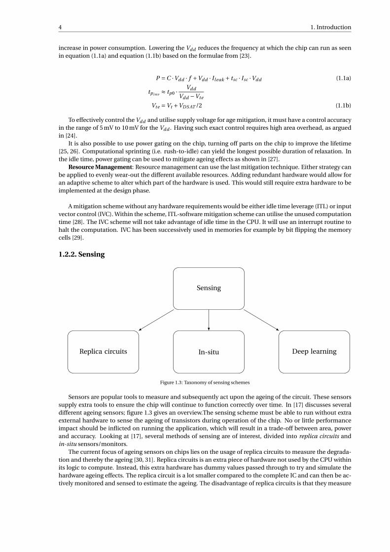
1.2.2. Sensing
Sensing
Replica circuits In-situ Deep learning
Figure 1.3: Taxonomy of sensing schemes
Sensors are popular tools to measure and subsequently act upon the ageing of the circuit. These sensorssupply extra tools to ensure the chip will continue to function correctly over time. In [17] discusses severaldifferent ageing sensors; figure 1.3 gives an overview.The sensing scheme must be able to run without extraexternal hardware to sense the ageing of transistors during operation of the chip. No or little performanceimpact should be inflicted on running the application, which will result in a trade-off between area, powerand accuracy. Looking at [17], several methods of sensing are of interest, divided into replica circuits andin-situ sensors/monitors.
The current focus of ageing sensors on chips lies on the usage of replica circuits to measure the degrada-tion and thereby the ageing [30, 31]. Replica circuits is an extra piece of hardware not used by the CPU withinits logic to compute. Instead, this extra hardware has dummy values passed through to try and simulate thehardware ageing effects. The replica circuit is a lot smaller compared to the complete IC and can then be ac-tively monitored and sensed to estimate the ageing. The disadvantage of replica circuits is that they measure

1.3. Contributions 5
the exact amount of ageing on the circuit less accurately [32]. This limitation is because the ageing of thecircuit is not measured, but the ageing of the replica circuit, which does not fully represent the ageing of theprimary circuit.
Besides replica circuits, in-situ sensors can be embedded into the chip [33, 34]. These in-situ sensorsdirectly measure the performance of the (sub)circuits to measure their ageing. A disadvantage of in-situsensors is that they can come with a significant area and power penalties [17]. However, their accuracy istypically higher, compared with the replica circuits.
Deep learningAs sensing the current sensing methods are not that accurate and require and high overhead. Recently, peoplestarted research into the usage of deep neural networks to predict the ageing of a complete chip by using afew sensors on the chip [35–37] to reduce this overhead. An advantage of this approach is that it can reducethe overhead of the sensing network significantly [17]. Reducing the required number of sensors within the ICreduces the overhead at which sensing comes. Deep learning can even use the BIST to sense the degradationof the chip [37].
1.2.3. State-of-the-art limitationsThe state-of-the-art analysis clearly shows that there is little work on software-based ageing mitigation schemesand in particular for static random-access memories (SRAMs). To the best of our knowledge only one schemehas been proposed for SRAMs [29]. In this work, the authors propose to periodically flip the contents of allmemory cells to balance the probability of storing a zero or one in them as this results in their lowest possibledegradation. Limitations of the above work and other work on SRAM mitigation are as follows: firstly, theyconsider only one component (the memory cell). However, as shown in [38], the ageing of different compo-nents of the memory affects other parts. Secondly, prior work typically uses SRAM and ageing models whichare relatively old and, thus, less accurate and relevant. Thirdly, most papers do not use realistic workloadsbased on real applications.
Besides the limited work on software-based mitigation schemes for the SRAMs, none of the literatureinvestigates the possible performance advantage of using sensors within the IC compared to time-based rou-tines. However, it can be expected that the use of sensors can also aid in improving the effectiveness of themitigation since the system can now monitor which parts degrade more and act with an appropriate response(e.g. by putting degraded parts more often into idle mode). Hence, this gives rise to the following sub researchquestion:
Does the use of ageing sensors improve the performance of software-based ageing mitigation com-pared to software-based mitigation that does not use sensing?
Besides the use of sensors, the built-in self-test (BIST) inside chips may also be an interesting tool to de-ploy for ageing mitigations. Using BIST to mitigate the hardware ageing, this would reduce the time overheadto mitigate hardware ageing. The BIST can be used to test the chip infield. During this testing, lots of patternsare applied to the circuit [39]. These test patterns have a pseudo-random nature when a linear feedback shiftregister (LFSR) is used to generate the vectors. Since different vectors are applied to the circuit, the circuit issubject to various workloads. Hence, it may be possible to adapt these vectors to mitigate the circuit ageingin the form of IVC. The literature study, however, yielded no research to adapt the BIST to apply input vectorcontrol (IVC) patterns to reduce circuit degradation and to apply Logic-Wear-Levelling (LVL). As the literatestudy did not yield anything about using BIST for ageing mitigation, it raises a second sub research question:
Can the test patterns in the BIST be altered to allow for mitigation against ageing?
1.3. ContributionsThis thesis proposes a software-based mitigation scheme for SRAM memories. The scheme is based on peri-odically flipping the contents of the memory cells reducing the duration of static stress periods is significant,resulting in a lower overall degradation of the SRAM memory. Additionally, this software-based scheme alsohelps to mitigate the ageing of the memory’s Sense Amplifiers. Besides the software mitigation scheme, ahardware mitigation scheme has been created and tested. The hardware mitigation works similarly to thesoftware scheme: it flips the memory cells to reduce the static stress duration. It also changes the averagestored value in the memory, such that the probability of storing a one or zero becomes equal. In short, thecontributions of this thesis are as follows:

6 1. Introduction
• Memory access model: The authors propose an analytical model to predict the memory access pat-terns and the workloads of the components inside the memory. Use of this model demonstrates thatthe expected static stress for the SRAM cells is non-negligible and, thus, a mitigation scheme is required(also proposed in this thesis).
• Software-based mitigation scheme: This paper proposes a mitigating scheme implemented in soft-ware. Using this software scheme makes it possible to reduce the BTI induced ageing effect in theSRAM cell and Sense Amplifier (SA). This mitigation scheme reduces the BTI in the memory cells up to2.5 times, and in the sense amplifier, the offset voltage is reduced up to 50%.
• Hardware-based mitigation scheme: The authors propose a mitigating scheme implemented in hard-ware, making it possible to reduce the BTI induced ageing effect in the SRAM cell and Sense Amplifier(SA). This mitigation scheme reduces BTI in memory cells up to 45 times and reduces the offset voltagein the sense amplifier up to 67%.
• Validation of mitigation schemes on a RISC-V platform for real applications.
• Improved ageing modelling over state-of-the-art: instantaneous or short-term BTI effect is included.
• Comparison between software-based and hardware-based mitigation schemes.
• The usage of BIST for mitigation of ageing within SRAM is not feasible.
• Using sensing to improve software mitigation scheme is not workable due to inaccurate and run timeconstraints.
1.4. Outline1. Chapter 2 provides background on the SRAM design.
2. Chapter 3 discusses the reliability failure mechanisms in CMOS, the prior work on SRAM reliabilitymodelling, and the state of the art of SRAM ageing mitigation.
3. Chapter 4 presents the developed mitigation.
4. Chapter 5 supplies the experimental results. Here, the authors evaluate and compare the performanceof both the software- and hardware-based schemes.
5. Chapter 6 gives the conclusion of this work and suggestions for future work.

2SRAM Design
This chapter provides background on SRAM design.
1. It gives a general overview of memories in computers.
2. It discusses the SRAM organisation and, subsequently, it discusses the most important SRAM metrics.
2.1. Computer memoryThere are two categories of computer memories: volatile and non-volatile. Volatile memories require powerto retain their stored data. Conversely, non-volatile memories do not require this; they keep their data evenwhen they are powered down. A disadvantage of non-volatile memories, however, is that they are slower thanvolatile memories. Therefore, for direct computations, ICs or processors use volatile memories, while forlong-term storage they use non-volatile memories.
The two most commonly used volatile memories are DRAM and SRAM. DRAM was the main memory ofcomputers and processors in the early stage of computing. However, the speedup of processors created amemory gap. This means that DRAM could not keep up with the speed of the processors [40] as illustratedin figure 2.1. The speed of the processor increased at a faster rate than that of the memory. To combat thismemory gap, caches were introduced. These caches are small(er) memories close to the processing unit thatcache data for fast access. SRAM typically implement these caches, which is faster than DRAM [41].
Figure 2.1: CPU-memory performance gap increasing over time, showing the need for faster and improved cache policies. Figure 1 from[1]
Fast memories need to be used, to counter the memory gap, otherwise the processor would be waiting fordata. Fast memories are available in the form of SRAM or DRAM. An overview of these memories is shown in
7

8 2. SRAM Design
table 2.1 [42]. Caches exploit the temporal locality and spatial locality to bridge the memory gap. Temporallocality refers to the fact that if a value has recently been accessed, the chances are high, it will be used againin the near future. Where as spatial locality refers if a certain value is accessed, it is expecting values closeto this value will be accessed next (e.g. a for looping traversing an array). As can be seen in the table thefaster the memory the more expensive the memory becomes. Moreover, RAM is volatile and does not allowfor permanent storage of data, which is done on flash that is much slower.
SRAM creates the L1, L2, L3 caches in the processor. The size of the memory cells limits the cache size.The bigger the cache becomes the slower the access will become [42].
Table 2.1: Comparing the different types of memories used in current computers
Parameters SRAM DRAM Flash
Volatile Yes Yes NoCell size Six transistors Single transistor and a capacitance Single transistor
Access time 0.5 ns to 2 ns 50 ns to 70 ns 5µs to 50µsWrite power Low Low High
Price per gb (2012) 500$ 10$ 1$
2.2. SRAM organizationThis section discusses the organisation and design of SRAMs. SRAM designs consist of multiple components,each taking care of a specific function within the memory. Figure 2.2 diagrams a typical memory design. Theinputs consist of control signals to select whether a read or write operation (r/w) should occur and an enablesignal to enable the operation of the memory. Other input and outputs are address lines and the data linesData In. The output signals consist of only data lines, namely Data Out. Some designs combine them withthe input lines. Combining the input and output lines reduces the number of pins on and the size of thememory chip, which makes the memory component cheaper.
data_out
enable
r/w
data_in
address
c_en
c_r/w
c_address
c_data_in
Input FFs
Cell Array
WL
Decoder
BL Mux
TimingSense AmplifiersLatch + Buffers
Write Drivers
sa_en
wd_endeco
der_
enab
le
wl
bl
wl
clk
Figure 2.2: Functional model of an SRAM component. Based on figure 1 from [2]
Figure 2.2 also shows the different memory that an SRAM module is typically composed of, which are asfollows:
• Memory cell array: responsible for storing the bit values of a word.• Address decoder: responsible for selecting the right memory cells during a read or write operation. It
typically consists of a column and row decoder.

2.2. SRAM organization 9
• Sense amplifier: responsible for converting the voltage, returned by the memory cells, to the corre-sponding bit values.
• Write driver: responsible for writing new values to the selected memory cells.• Data-Out and Data-In registers: buffer to stabilise the in-and-output values.• Timing: will generate the control signals to enable the write or read circuit at the right moment in time.
A brief description of each component follows.
2.2.1. Memory cell arrayThe memory cell array handles storing the data. It is composed of memory cells, which are the essential partof any memory. The SRAM memory cells are based on bistable circuits. The conventional SRAM cell uses sixtransistors (i.e. the 6T SRAM cell) shown in figure 2.3. It consists of a cross-coupled inverter pair (M1 and M2
and M3 and M4) which serves as the bistable element.When writing to or reading from the memory cells, the WL must be driven high, ensuring access through
pass transistors M5 and M6 to the cross-coupled inverters. Writing to a memory cell is then done by drivingthe values on BL and BL. During the write operation the bit lines must be driven with enough power toovercome the cross coupled inverters. As a result, the cross-coupled inverters will flip the stored values and,thus, a new value is successfully written to the cell. Reading data from SRAM is done by first pre-charging thebit lines to a high value. After enabling the word line, the inner nodes Q and Q will be connected to the BL andBL. As a result, the memory cell will then pull one of the bit lines low. Afterwards which the read circuit canamplify the read value. The Sense Amplifier performs this amplification; which is discussed in section 2.2.3.
Figure 2.3: A conventional six-transistor SRAM cell
2.2.2. Address decoderThe address decoder decodes the input address, such that the read or write operation is performed for thecorrect memory cells. Typically, the memory array is divided into selectable rows and columns. A row decoderselects the rows, also often called the WL, and the column decoder selects the columns. Therefore, memoryaddresses are typically divided into high and low order bits. The advantage of using both a wordline decoderand a column decoder is that the individual decoders require less hardware and are, thus, faster. The higherorder bits are typically used by the row decoder and the lower order bits by the column decoder.
2.2.3. Sense amplifierThe Sense Amplifier (SA) is responsible for the memory’s read operation. The SA amplifies the small voltagedifference at the bit lines generated by the memory cells. Figure 2.4 shows the schematic of the standardlatch-type Sense Amplifier, which is a popular design and will, therefore, also be the focus of this work. The

10 2. SRAM Design
operation of the SA consists of two phases. The first phase is the sensing phase, followed by an amplifica-tion phase. The sensing phase will read the voltages of the BLs. In this phase, signal SAEnable is low whichactivates the Mpass and the Mpass to pass through the voltage of the bitlines to the SAOut and SAOut. Thesecond phase is started by the timing component which will make sure the SAEnable signal is high when dis-connecting the SA from the bitlines and enable the cross-coupled inverters. The cross-coupled inverters willthen amplify the voltage difference between SAOut and SAOut. After completion the full-swing read value isavailable on SAOut and its inverse at SAOut.
SAEnable
Mup Mup
Mdown Mdown
SAEnable
Mtop
Mbottom
SAEnable
BL BL
SAOut SAOut
Mpass Mpass
SAEnable
Figure 2.4: Sense Amplifier
2.2.4. Write driverThe write driver manages the memory’s write operation. It achieves this by driving the bit lines. Figure 2.5shows an example write driver. The first stage of the write driver is receiving input on the Data_in line afterwhich Data_in will pass through one inverter to create an inverted signal Data_in for the BL. This signal willthen pass through a second inverter to create the signal for the BL. The control circuit will then finally enablethe write driver by toggling the Write_enable signal high. The Write_enable will let the transistors Q1 and Q2pass the value towards the bit lines which then will propagate to the memory cell. Strong inverters are usedwithin the write drivers to ensure that it can drive the high parasitic capacitance of the bit lines.
2.2.5. Timing circuitThe subcomponents of the memory require several control and timing signals to make the complete compo-nent work. The timing circuit controls the memory to allow every subcomponent to work in harmony. Thesesignals are all generated by the timing component.
2.3. SRAM metricsThis section gives a brief overview of the memory’s metrics. Figure 2.6 shows a classification diagram ofthe different SRAM metrics. The SRAM metrics can be divided into functional and parametric metrics, asproposed in [3]. More detailed subdivisions for both the parametric and functional metrics are given in fig-ures 2.7 and 2.8, respectively. The figures shows the different metrics for every component of the memory.The division into functional and parametric metrics is motivated by [43]. Functional reliability refers to thecorrectness of the system (i.e. the system gives the correct output values). For example, a bit flip in an SRAMcell is a functional error. In contrast, the parametric metrics evaluate the performance of the memory whichdoes not directly affect the correct functionality of the memory. An example of a parametric metric would bethe speed at which the memory cell can discharge one of the bit lines. This study focusses on mitigating theageing of the memory cell and the sense amplifier. Therefore, the authors will only discuss these metrics.

2.3. SRAM metrics 11
Figure 2.5: Simple write driver showing how enough drive strength can be created to successfully change the value of the bit lines.
Memory metrics
Parametric Functional
Figure 2.6: Classification diagram of the different memory metrics, based on [3].

12 2. SRAM Design
Parametric
Overall Cells Address decoder Write cicruit Sense amplifier
Read timingWrite timingPower
Discharge delay WL delay Write delay Sensing delay
Figure 2.7: Classification diagram of the different parametric memory metrics [3]. The round boxes denote the components, while thesquare boxes at the bottom list the corresponding metrics.
Functional
Overall Cells Address decoder Write cicruit Sense amplifier
Failure rate
BL swingHold static noisemargin
Setup margin Write margin Sensing margin
Figure 2.8: Classification diagram of the different functional memory metrics [3]. The round boxes denote the components, while thesquare boxes at the bottom list the corresponding metrics.

2.3. SRAM metrics 13
2.3.1. Memory cellThe memory cell is responsible for storing a binary value, which it needs to maintain reliably over time. Ad-ditionally, it needs to allow the value to be read without causing any bit flip. Hence, the memory cell needsto be stable. It also needs to generate a sufficient bitline discharge, such that the sense amplifier can am-plify this value into a full-swing logic value. Figure 2.7 illustrates that the memory cell’s parametric metric isthe discharge delay. The functional metrics of the memory cell are its BL swing, its hold-static noise margin,and its read-static noise margin, as shown in figure 2.8. Next, the authors will discuss both parametric andfunctional metrics of the memory cell.
Figure 2.9: Example voltage of a memory cell showing the hold and read static noise margins.
Parametric metricsThe memory cells read and write values into memory. For the memory cells the discharge delay is the metricused to define the parametric metric. This delay defines how long the sense amplifier needs to wait beforeit can start to process the voltage difference on the BLs. Figure 2.10 shows the discharge delay. The delaydenotes the duration after the wordline was activated and one of the two BLs is discharged for 10%.
Functional metricsThe functional metrics for the memory cell is how much noise the memory cell can tolerate during a readoperation. The SNM is shown in figure 2.9. The read SNM decreases compared to the hold SNM becauseof writing the cell value to the BLs, called the hold SNM. The write performance of the cell is not taken intoaccount. The memory cell must be able to be written to, which is tested at the production of the memorywherein the write performance improves over time [44]. Since the cell writes performance improves, it is notinteresting to measure this during the evaluation of the ageing of the transistors.
2.3.2. Sense amplifierAfter the memory cells have slightly discharged one of the two BLs, the sense amplifier will use the voltagedifference as an input to convert into digital value to be used as the output of the memory. The sense amplifier

14 2. SRAM Design
Figure 2.10: Discharge delay of the memory cell.
is, ideally, balanced and thus will convert a negative voltage difference to a zero value and a positive voltagedifference to one. However, if the offset voltage of the sense amplifier is not zero, it will have a preference toconvert to one of the two bits values. In most cases, the offset voltage is not zero due to ageing and processvariations [45]. Figure 2.11 presents the offset voltage effect as an added voltage source on the input line of theBL. The added voltage source will reduce the voltage difference between BL and BL. If the voltage differencecomes under the voltage threshold which the sense amplifier requires, the result is an incorrect output value.
Figure 2.11: Offset voltage model for the sense amplifier an extra voltage source is added on the BL input. The added voltage source canreduce the voltage difference between the two BLs this voltage source can then result into an incorrect read value on the output.
Parametric metricsThe sense amplifier will read the input from the BLs and convert this value into a binary value which theprocessor can use. For the parametric metric of the sense amplifier, one needs to look at the sensing delay.The sensing delay is related to many factors. In figure 2.12, the sensing delay is shown together with thesensing margin. The sense amplifier is enabled by the timing circuit when the difference between the two bitlines is larger than 10%. The sensing delay is then the amount of time it takes to reach half a swing.

2.3. SRAM metrics 15
Figure 2.12: Sensing delay and sensing margin of the sense amplifier.
Functional metricsAs the sense amplifier reads a voltage offset from the two BLs which is relatively small, the sense amplifierneeds to convert this value to the correct value. If the sense amplifier would have too big of an offset on thedecision threshold it might decide to convert the voltage difference to the wrong value. The offset voltage isthe most important metric and will be the only metric used for the sense amplifier in this work.


3Overview on SRAM Reliability Modelling
and Mitigation
This chapter discusses reliability issues and application to SRAM. It also explores the state of the art on howto mitigate reliability issues:
1. The authors discuss the different failure mechanisms in section 3.1, followed by a discussion on howthese reliability challenges and failure mechanisms can be modelled for SRAMs in section 3.2.
2. Section 3.3, the authors discuss the state-of-the-art mitigation schemes and explore their advantagesand disadvantages.
3.1. Failure mechanisms of transistorsIn figure 3.1 a classification of the different reliability failure mechanisms is shown, based on the work of Agbo,Innocent in [46]. The reliability failure mechanisms can be divided into two categories: time-zero defectsand time-dependent defects. Process variation causes the time-zero defects. Process variation can be ondifferent scales; for example, a single chip within a wafer has a degraded performance or a complete waferhas degraded performance. Within the thesis, the focus will be on time-dependent failures. Environment-induced failures are out of scope for this thesis as they are the inputs where the system runs and cannot bereliably mitigated on-chip: voltage (for example voltage spikes) and temperature changes. As ageing failuresare relatively new, the authors will list the mechanisms first, followed by an in-depth explanation of each. Asshown in figure 3.1, the ageing related failure mechanisms are as follow:
• Bias Temperature Instability (BTI)• Random Telegraph Noise (RTN)• Time-Dependent Dielectric Breakdown (TDDB)• Hot Carrier Injection (HCI)• Electromigration (EM)
3.1.1. Bias Temperature InstabilityBias Temperature Instability (BTI) is an ageing mechanic which increases the absolute Vth value and de-creased drain current of the transistors [46]. The BTI mechanism is active when the transistor is switched on.There are two different types of BTI: Negative Bias Temperature Instability (NBTI) and Positive Bias Tempera-ture Instability (PBTI). NBTI affects PMOS while PBTI affects NMOS. BTI is the most relevant ageing mechanicin memory [47, 48]. This is because memories perform relatively little switching and, thus, some transistorsare turned on (hence, the BTI mechanism is active) for long periods and, thus, degrade significantly.
While the effect of NBTI is the most significant of the two, PBTI is becoming more and more prevalentdue to the scaling of the transistors [17]. As said in [14, 15, 44, 49–51], the effects of BTI on the lifetime isa function which takes into account duty cycle, temperature, signal probability (zeros, ones, state switches)and the supply voltage (Vdd ). BTI consists of two phases a recovery and a stress phase. The effect of thesephases are shown in figure 3.2. Over time the BTI effect builds up due to partial recovery.
17

18 3. Overview on SRAM Reliability Modelling and Mitigation
Reliabiltyfailures
mechanisms
Time zero(Spatial/Process) Time dependent
Local (intradie) Global (interdie) Enviromental Temporal/Ageing
Front-end Back-endLot-to-lotWafer-to-waferDie-to-Die
RDDLERMGGOTV
VoltageTemperatureSoft-error
Back-end Front-end
BTIHCITDDBRTN
EMTDDB
Figure 3.1: Reliability failure mechanisms classification
Figure 3.2: Bias Temperature Instability voltage threshold shift during stress and relaxation. Figure based on [4]
In [52], the two models are compared. They show that while the atomistic trap model is more accuratethan the Reaction-Diffusion (RD) model, its simulation time is limited to a scale of just seconds. The RDmodel is less accurate but is good enough to show the ageing over a long timescale. The author suggestsusing both models in conjunction to allow for faster simulation. The physics of BTI are not fully understoodas two models are used to describe the BTI-effect.
Reaction-Diffusion ModelThe Reaction-Diffusion (RD) model focuses on the breaking and healing of Si – H bonds [53]. The reactionpart of the model focuses on the chemical reaction of the Si – H bonds at the interface. During the stressphase of BTI, these bonds break; during the relaxation phase, these bonds can recover. The second part ofthe RD model focuses on the diffusion of the hydrogen atoms. The bondage breakages in the Si – H result indangling bonds in the silicon oxide which will create a threshold voltage shift due to the trapping of charge atthe silicon interface [54]. When removing the electrical field, some of the hydrogen atoms will diffuse back,resulting in a reduction of the voltage threshold shift [55].
Atomistic Trap ModelThe RD model can be inaccurate in [56]. To improve the accuracy of the BTI modelling the atomistic trap-based model was introduced by [57]. The model is based on the capture and release of single traps. Thesetraps or defects are created because of the production process. Each trap introduces an δVth which canrestore itself overtime during the relaxation phase [52].

3.1. Failure mechanisms of transistors 19
3.1.2. Random Telegraph NoiseRandom Telegraph Noise (RTN) is a stepwise ageing effect due to which carriers are injected into the oxidelayer. The RTN occurs as random events over time and it is unpredictable when it will occur. In [58], RTN isdescribed as traps creating leakage currents. Traps formed in the high-k material create this leakage current.As more traps build up over time, a hard breakdown will eventually occur. RTN is a switching phenomenon[59]. Since memories are mostly static, the effects of RTN will be limited.
3.1.3. Time-Dependent Dielectric BreakdownIn [60], the process of Time-Dependent Dielectric Breakdown (TDDB) is described as when the device is un-der a constant electric field, but less than the material breakdown field strength, the transistor gate-oxide willstill breakdown over time. TDDB consists of three-phases [55]. At first, a soft-dielectric breakdown can occurfollowed by a progressive-dielectric breakdown. At the last stage, a hard-dielectric breakdown occurs. Soft-dielectric breakdown causes partial loss of the dielectric properties, resulting in lower gate currents comparedto the next stages. The progressive-dielectric breakdown can be detected by a slow increase in gate currentover time. When the hard fault occurs, the gate current rises to the mA at the standard voltage levels [55].
3.1.4. Hot Carrier InjectionHCI is caused by the acceleration of carriers (holes or electrons) under the force of the electrical field at whichthe momentum is high enough that the carriers break the barriers of surrounding dielectric and get trappedin the gate and sidewall oxides [61]. The acceleration and breaking of bonds are visualised in figure 3.3.
Hot Carrier Injection is an ageing effect which will increase the Vth . The Vth shifts due to the injectionof carriers into the gate. This injection happens when the gate voltage of the transistor switches. In [48] HotCarrier Injection (HCI) is described in relation to the effects of BTI in memory. This study reveals that HCIhappens when a bit is flipped (and, thus, the gate voltage switched), while BTI is a static ageing mechanic. Theresults of [48] reveal that adding HCI simulation to the model yields a slight improvement in the performanceof the memories over time.
Figure 3.3: Hot Carrier Injection bond breakage towards the end of the channel. Figure from [5]
3.1.5. ElectromigrationElectromigration (EM) is an ageing failure mechanism for the interconnects in the chip [62]. Due to theincreasing current densities within the wires on the chip, metal ions can be displaced. The displacementof the metal ions results in voids and hillocks. In figure 3.4, an example is shown of the effect of EM, creatingthe voids and hillocks. The voids within the wire will create open connections while the hillocks can createshorts. In [63] several mitigation schemes for EM are described. Mitigation of electromigration can be doneeither by taking it into account during the design or by using bi-directional currents [64] during the operationof the IC. A disadvantage of bi-directional power is that the design requires changes to accommodate for this.
Figure 3.4: The result of hillocks and voids created by electromigration. Figure from [5]

20 3. Overview on SRAM Reliability Modelling and Mitigation
3.2. SRAM Reliability ModellingThis section briefly discusses state-of-the-art in SRAM reliability modelling. This modelling is important as itallows one to estimate the impact of ageing during the design and, proper measures can be taken. This willlead to a more reliable design at reduced costs. Figure 3.5 gives an overview of SRAM reliability modelling.The, SRAM reliability modelling consists of three major parts:
SRAMReliability
Circuit
Variability
Analysismethod
Cell array
Peripheral Circuitry
Partial/Complete Memory System
Process, voltage, and temperature (PVT)
Ageing
Non-Statistical
Monte-Carlo
Failure region sampling
Analytical modelling
Figure 3.5: Reliability flow of SRAM
• Circuit: this can be either a single SRAM cell, one of the peripheral circuitries or a partial or completememory system.
• Variability: several types of variability have an impact on the memory system. These are process, volt-age, and temperature (PVT), and ageing.
• Analysis method: different methods exist to estimate the reliability of a system. Each model comes withits advantages and disadvantages. The different methods consist of non-statistical methods, MonteCarlo simulations, failure region sampling, and analytical modelling.
This thesis will discuss the memory cell reliability and peripheral circuit containing the read-write circuitry.
3.2.1. Memory cell arrayMost of the prior works focused on modelling the reliability of the memory cells, specifically on PVT. The mostused simulation method is based on the Monte Carlo approach. Less work exists on ageing modelling of thememory cells. This thesis will focus on the ageing aspect due to BTI, which is the most important ageing effectin transistors. Most studies use non-statistical methods to estimate the impact of BTI. The non-statisticalapproach usually underestimates the ageing effects. In the papers [65–67] ageing impact is analysed in thememory cells. Of these papers, only [67] analyses the failure impact due to ageing in SRAM cells. They use anon-Monte-Carlo simulation method which looks at the possible Vth shifts. This method allows for a moreaccurate simulation of BTI impact compared to the old statical method of expected Vth shift. This allows anaccurate representation of when a memory cell could fail if the correct workload is taken into account.
3.2.2. Peripheral circuitry and partial or complete memory systemSignificantly less work exists on the reliability modelling of the memory’s peripheral circuitry compared withthe memory cell. Within the works of [68, 69] ageing of the sense amplifier has been analysed. Within [70, 71]the write driver and the ageing of the timing circuit are analysed.
3.3. SRAM Mitigation 21
There is even less research on the reliability modelling of the partial or complete memory system. In [72],an analysis is made how ageing impacts the cell and Sense Amplifier, including their interactions. In [73],a complete SRAM circuit is analysed. These works are limited; by that the authors do not examine how theindividual components contribute to the ageing.
3.3. SRAM MitigationIn section 1.2, the study investigated several mitigation schemes, but it has not been translated to mitigationsfor SRAM. This section will go into more detail on how mitigation schemes can be applied to SRAM.
An overview of the different mitigation schemes is given in figure 1.2. There are two categories of themitigations and adaption techniques: mitigation at design-time and mitigation at run-time.
3.3.1. Mitigation at design-timeThese schemes are static and can be implemented in different ways. The first way of mitigating the effects ofageing is by adding extra hardware to create a margin for chip degradation [12, 13]. These novel implemen-tations are known as a worst-case design [13] and can be improved upon by looking at [74] and running abetter-than-worst-case design. The better-than-worst-case design can be used because chips will not alwaysbe under maximal stress.
Worst-case design strategyThe method worst-case-design requires the usage of extra hardware either by resizing the size of transistorsor reducing the operating frequency of the chip which creates a margin where the chip can accommodate theeffects of BTI. Applying worst-case-design to SRAM is highly inefficient and costly as the memories consumethe largest part of the die. Most added silicone would not be used during the lifetime of the chip.
3.3.2. Better-than-worst-case design strategyThe static methods require advanced knowledge of the workload and analysis of the stresses occurring inmemory, to improve on the method worst-case-design. In this scheme on memory, while having the mostageing, can be resized either by creating unbalanced cells, so the cell is tailored more towards the storage of azero or a one-bit value. This technique is introduced in [75] to counter the differential ageing of SRAM-cells.It will reduce the required hardware overhead compared to worst-case-design [14, 15]. Mitigating the ageingeffects of transistors running different workloads require having different library cells for each expected life-time and load [16]. For SRAM, it would require to have different memory cells within the cell array to handlethe unbalanced workloads. This will create an inefficient, memory, cell-array structure. If the workload be-haves differently from the expected workload, it can create a much faster degradation in the memory cellscompared to not having implemented any mitigation scheme. This will be the case if the workload simu-lation suggests placing smaller, weaker cells at a certain location, which will then result in having a higherthan average static stress [17]. As staid in the state of the art, the halting problem does not allow solving theproblem, not knowing upfront how the memory stresses will be distributed.
3.3.3. Mitigation during run-timeDuring the run-time of a chip, the usage of dynamic schemes is possible to reduce the BTI-induced ageingeffects within the memory. These dynamic schemes will apply resource management either to reduce theamount of static stress, which occurs or to relax the parts of the memory which are under the most stress.There are different techniques, which can mitigate BTI-induced ageing effects these are:
• Idle time leverage (ITL)• Input vector control (IVC)• Controlled resource wear out• Spatial redundancy
Idle-time leverage and input-vector controlAs a chip usually does not use all resources at all times due to stalls (structural-, data- and control -hazards)and a program does not always require maximum performance, analysis of programs is made in [76]. Withinthe time that a CPU has a stall or is not fully used, recovery schemes can be executed to reversed to mitigatethe effect of BTI. Schemes taking advantage of this are of the category ITL. ITL scheme can be extended withthe usage of IVC to control the mitigation of, for example, BTI-induced ageing.
22 3. Overview on SRAM Reliability Modelling and Mitigation
Input vector control (IVC) can be an effective technique to reverse and mitigate the effect of BTI in thechips. The mitigation scheme can either run in available idle or by stalling the execution of the program. Thezero-value cause in the PMOS transistors creates BTI-wear [77]. To determine which bit value should be usedin idle time requires estimating the degradation of transistors. The process of estimating the degradation ishard due to variation in the operating temperature and settings. In [78], artificial intelligence techniques areused to find an optimal program which yields the best BTI rejuvenation program to be run on the CPU.
IVC can be applied by the usage of NOPs within the CPU. The usage of alternative NOP instructions hasbeen analysed in [28] to see if this can reduce the effect of BTI-wear. When using idle instructions in theexecution, a part of the work can be offloaded to the compiler, as it can detect some stalls and idle timesat compile-time. The usage of IVC by using a different instruction for the NOP is not possible for the caseto mitigate stress in memory cells. The NOP instruction is not allowed to have side effects and thus cannotalter a register value or change a memory value. As it is not possible to read a single memory value, relaxthe cells, restore the cells, and restore the register state within one clock cycle, it is not feasible for memorycomponents.
A different technique of mitigating BTI-induced ageing bit flipping is introduced. Bit flipping is used toreduce the stress in the memory components as described in [29]. Bit flipping is a unique form of IVC asthe vectors are based on the current values in memory. Flipping the bits in memory ensures the zero andone-bit value have the same occurrence chance. A software and hardware approach are discussed in [79]for the flipping of bits in SRAM. The limitations are that using the CPU to flip the bits will cost too muchtime for the L3 cache. To improve the results of bit flipping [80] proposes the Cell Flipping technique withDistributed Refresh phases (CFDR). CFDR reduces the time required for flipping the memory bits by changingthe frequency at which individual cells are flipped. Using information from the workload allows for a smalleroverhead. The disadvantage is that it requires advanced workload knowledge, and it has to consider thehalting problem. It would require the ability to determine the control flow of the program upfront for all thedifferent inputs available, to find the best solution for the mitigation scheme. In 1936, Alan Turing provedthat this is not possible.
Controlled resource wear-out and spatial redundancyAs dark silicon is starting to get introduced [81] more and more parts of the chip cannot always be active dueto the power wall [82]. Smart schemes can be created to add extra hardware, which can be used to extend thelifetime of chips. In [83, 84] computational sprinting is described, which allows for bursting the speed of aCPU past the thermal power limit by using a different set of cores. Since computational sprinting is used, thetask is completed faster than expected. The generated slack can then be used to power-gate several parts ofthe chip. Power-gating will then allow for the recovery of the BTI effect.Another option to control the wear-out of the chip is using spatial redundancy. Spatial redundancy addsredundant hardware which can be used via software or on-chip logic. For example, the scheme Logic-Wear-Levelling (LVL) [85] allows software routines to switch critical paths to the redundant paths, which are avail-able to allow the transistors to recover.
Applying computational sprinting within SRAM only, will not work as the memory is only supplying theCPU with value when requested and is already mostly idle. It is not able to mitigate, but by just doing nothing,the bit value will be maintained in the memory cell. Using the advantage of dark silicon within SRAM wouldbe possible. For example, when a part of the memory breaks a smart control logic can replace the faulty wordor use a logic scheme to alter the write locations of a word from the main memory to the dark silicon. Whenmaking use of the dark silicon, this will not limit the usage of a software mitigation scheme or a hardwaremitigation scheme, which will try to mitigate BTI-induced ageing actively.

4Mitigation Methodology
This chapter will introduce mitigation schemes:
1. Section 4.2, the authors created and analysed a model for static stresses.
2. Section 4.3 uses the results from the modelling of the stresses in the memory to discuss different possi-ble mitigation schemes.
3. Section 4.4 and section 4.5 examines software, and hardware mitigation schemes and the authors cal-culate how feasible each scheme is.
4.1. Static stressWhen looking at SRAM memory, it is important to know which static stresses occur in memory, as a singlesecond of static stress creates a high amount of ageing. Reducing the duration of the static stress slightlyalready yields a large improvement. In [4], the initial recovery is discussed showing that even a short amountof relaxation will significantly reduce the BTI in the transistors. The transistor should not be stressed too long,as that will greatly increase the required relaxation time, which is needed to recover from the BTI effects. Infigure 4.1, the authors conduct a sweep of different duty factors showing the effects this has on the Vth shift.Short static stress of 1 s already changes the Vth shift with 4 mV. Adding a small relaxation would ensure thisstress does not occur.
0 10 20 30 40 50 60 70 80 90 100
Duty factor
-68
-66
-64
-62
-60
-58
-56
Delta V
th in m
V
Duty factor sweep of duty factors for 1 second after three years at a duty factor of 0.5 and 125 degrees
Figure 4.1: A duty factor sweep is conducted after ageing a transistor for three years at 125 C. The ageing is extended with one year toshow the effect of different stress values on the transistors. The duty factors which are at the extreme have a large impact compared to
the other duty factors.
4.2. Memory access modellingAs seen in section 4.1, static stress is by far the most important stress to be considered related to the ageingof SRAM. From the literature review, [86–89], a majority of papers in literature find that on average 10% of
23

24 4. Mitigation Methodology
the instructions are memory writes and that 20% of the instructions are memory reads. Using the Linux toolperf allows one to monitor the L1-cache usages. As expected, different workloads have different footprints inmemory usage. When using the perf tool to monitor Libreoffice (an office suite) 1, the memory instructionis around 10% memory writes, and 20% reads. When perf analyses the generation of prime numbers and itis run for a to create a varying amount of prime numbers the memory writes drop to 1.2%.
If static stresses are not taken into account and assume memory writes to be random, it is possible tomodel this using a Poisson distribution or Markov model, allowing the creation of a model for memory usage.Markov model analyses expected duty factors, while the Poisson model analyses static stresses in the memory.
Markov modelSimulating the memory as a Markov model gives insight into the operations of memory. Figure 4.2 shows thesimple cell states with the available transitions.
The different actions that can happen every clock cycle are:
• Value 0 is written• Value 1 is written• Cell is read• Cell is left idle
The state of the cell will only change if a value is written, which is the opposite value of the current cellvalue. When taking into account the number of words in the memory and assuming all memory actions arerandom based. The bit distribution is estimated to be non-random and favouring a zero over a one-bit value.The Markov model can be run to simulate possible memory stresses.
Cell value 0 Cell value 1
Figure 4.2: Markov model to describe the memory model
However, the Markov model is not exact, and it is computationally expensive to gather results from it.Since we are interested in how long the static stress state can be within a cell, one can look at when transitionsoccur. The authors suggest to use a Poisson model to calculate the chances for expected static stresses.
Poisson modelThe assumption is that memory write addresses, are random, and the written value is sampled from a randomdistribution. This is possible because of how one uses memory, for which the law of large numbers [90] canbe applied.
If one only considers the writes to the memory, this can be modelled as a Poisson process. The examplefrom the prime number generation provides these units to use within the simulations:
• Memory size 32 KiB• Word size 8 bytes• Frequency 1 GHz• Pwr i te = 0.012• P f l i p = 0.01
Pwr i tecel l = Pwr i te · W or dsi ze
Memor ysi ze(4.1)
λ= t ·Pwr i tecel l ·F r eq ·P f l i p (4.2)
1A open office suite which is an alternative to Microsoft office

4.3. Concept of the mitigation scheme 25
Pstr ess (t ) = e−t ·Pwr i tecel l·F r eq ·P f l i p (4.3)
This results of an expected static stress duration which can continue up to multiple seconds. Besidesthe normal static stress, prolonged static stress can also occur due to non-random events in a program. Forexample, when encrypting a message, the encryption key will stay in the cache during the encryption pro-cesses. The extended static stress needs to be measured by using benchmarks which simulated real-worldapplications. Which is what we analyze in chapter 5.
4.2.1. ConcludingThe random approach appears optimistic about the expected static stress duration in the SRAM cells, asnon-random events are not considered, which could create static stress for much longer than a few seconds.However, static stresses of multiple seconds can occur, which could be problematic for the lifetime of SRAM.It is expected that there would also be more static values in the memory with certain workflows, such asencryption where the encryption key remains in memory for a longer time. In these situations, mitigationwould be of even more importance.
4.3. Concept of the mitigation schemeStatic values induce ageing in SRAM in memory cells. The most optimal memory usage would be a perfectbalance between zeros, ones, and a short duration of static stress values.
Reducing the wear and ageing effects can be done by adding mitigation schemes to improve the lifetimeof the SRAM. Mitigation schemes will target the duration of static stress. By reducing the maximal static stressin a fixed amount of time, it is possible to utilise the fast initial recovery of BTI effects [57]. Reducing staticstress is best done with the usage of IVC patterns, as it has a small overhead in the execution of a programand makes sure the static stress sequence is broken. Due to a small overhead, the duty factor of a memorycell does not change by much. This is shown in equation (4.4).
dut y_ f actormi ti g ated ≈ dut y_ f actor · ttot al
ttot al + tmi ti g ati on≈ dut y_ f actor (4.4)
A different approach is to balance the stored value in memory such that the Pone = 0.5, which is possibleby adding a large overhead with a stall or by using hardware which could use pointers to keep track of whichparts of the memory are altered. Adding a large execution overhead would require doubling the executiontime to reach a Pone = 0.5. As such, this is not feasible, and only the hardware mitigation scheme can generatea completely balanced memory usage. The hardware scheme can then be implemented as a cyclic flippingscheme which will be described in more detail in section 4.5.
4.3.1. BTI effect in a transistor and mitigation potentialIt is important to understand the impact on a single transistor and see if a mitigation scheme will have apositive impact on the transistor, when analysing the effects of BTI. Several different experiments are runto establish the effects of the environment on the transistors. The different mitigation schemes are run ona single transistor, also analysing frequency and simulation accuracy. For the transistor, the study uses the14 nm model from IMEC, creating the transistor workload is done in the form of CDW format. Within theCDW format the duration, duty factor, and frequency are specified. In MATLAB a modelling platform wascreated where mitigation algorithm could be created allowing to run several different mitigation schemes:
• Baseline• Periodic mitigations
– Periodic insert idle time (software)– Periodic flip the transistors states (hardware)
Each of these implementations will come with different amounts of execution and/or hardware overhead.The simulation will be run for three years at 125 C. Simulating at an high temperature is the similar to a lowertemperature over a longer period. Higher temperature induces faster ageing due to the sped up reaction pro-cess.
The BTI model from IMEC works in the bracket:
• Vdd at 0.8 V ±10%

26 4. Mitigation Methodology
• Time step between 1×10⁻⁹ s to 1×10⁸ s• Frequency 1 GHz is realistic but in a range between 1 Hzand3×109 Hz• Temperature −40 C to 125 C
Frequency impactThe impact of frequency on the ageing is related to the duration of static stress. When reducing the frequencyat which the transistors run, will extend the static stress durations. If the duty factor of the transistor is eitherzero or one, it does not matter if the operating frequency changes. To verify this assumption, the BTI-modelof IMEC is used. Table 4.1 shows the results. In the extreme case where the duty factor is one, the frequencydoes not matter. When the duty factor is not in the extreme, the frequency does have an impact on thedegradation.
Table 4.1: Vth shift after three years showing the effect of using different clock frequencies on the degradation of a transistor.
Frequency Duty factor Degradation
1 GHz 1 −83.6 mV ± 0.42 mV1 kHz 1 −83.6 mV ± 0.39 mV1 GHz 0.9 −68.5 mV ± 0.64 mV1 kHz 0.9 −71.4 mV ± 0.62 mV
Simulation accuracyThe model of IMEC allows using average duty factors to speed up the calculation of the BTI impact on thetransistors. Using the average duty factor will result in degradation, which is similar (on average), but theworst-case performance could be different. The worst-case will decide at which moment the device will faila timing constraint. This effect can be mitigated by accurately simulating the last part of the workloads. Intable 4.2 this effect is calculated in more detail. The simulation accuracy is illustrated in more detail in fig-ure 4.3 shows, which results into a difference of up to 3.6 mV after 1×10³ s. The graph shows, the effect of fastdegradation and fast recovery. To determine the ageing it is required to look at the worst-case performanceand not to the average response as a metric violation will happen at the first point in time where the worstcase degradation point passed the toleration value.The MATLAB code, written and created for this project, will find the most optimal and accurate simulation ofthe workloads as possible.
99 99.1 99.2 99.3 99.4 99.5 99.6 99.7 99.8 99.9 100
Time in s
-16
-14
-12
-10
-8
-6
-4
-2
0
Delta V
th in m
V
Compare accuracy of different simulation strategies
Acurate duty factor simulation
Average and accurate duty factor simulation
Average duty factor simulation
Figure 4.3: Simulating a workload with an average duty factor of 0.5. It is shown that there is a big difference in the average simulationand the other two more accurate simulations. The difference between the two more accurate simulations is due to the stochastic nature
of the BTI process
Mitigation scheme performanceAfter setting the baseline related to the importance of how the MATLAB simulation should run and the im-portance of frequency, it is important to see if the mitigations schemes can work and reduce the ageing effectinduced by BTI. To analyse this the hardware flipping and idle-time injection are ran and compared in ta-ble 4.3. Each scheme yields a significant reduction in BTI ageing.
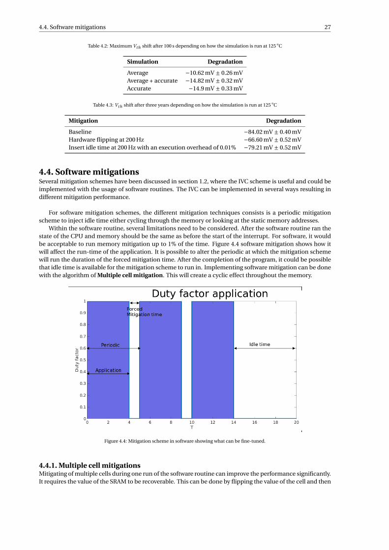
4.4. Software mitigations 27
Table 4.2: Maximum Vth shift after 100 s depending on how the simulation is run at 125 C
Simulation Degradation
Average −10.62 mV ± 0.26 mVAverage + accurate −14.82 mV ± 0.32 mVAccurate −14.9 mV ± 0.33 mV
Table 4.3: Vth shift after three years depending on how the simulation is run at 125 C
Mitigation Degradation
Baseline −84.02 mV ± 0.40 mVHardware flipping at 200 Hz −66.60 mV ± 0.52 mVInsert idle time at 200 Hz with an execution overhead of 0.01% −79.21 mV ± 0.52 mV
4.4. Software mitigationsSeveral mitigation schemes have been discussed in section 1.2, where the IVC scheme is useful and could beimplemented with the usage of software routines. The IVC can be implemented in several ways resulting indifferent mitigation performance.
For software mitigation schemes, the different mitigation techniques consists is a periodic mitigationscheme to inject idle time either cycling through the memory or looking at the static memory addresses.
Within the software routine, several limitations need to be considered. After the software routine ran thestate of the CPU and memory should be the same as before the start of the interrupt. For software, it wouldbe acceptable to run memory mitigation up to 1% of the time. Figure 4.4 software mitigation shows how itwill affect the run-time of the application. It is possible to alter the periodic at which the mitigation schemewill run the duration of the forced mitigation time. After the completion of the program, it could be possiblethat idle time is available for the mitigation scheme to run in. Implementing software mitigation can be donewith the algorithm of Multiple cell mitigation. This will create a cyclic effect throughout the memory.
Figure 4.4: Mitigation scheme in software showing what can be fine-tuned.
4.4.1. Multiple cell mitigationsMitigating of multiple cells during one run of the software routine can improve the performance significantly.It requires the value of the SRAM to be recoverable. This can be done by flipping the value of the cell and then

28 4. Mitigation Methodology
writing this value back. Using the negated value of the cell also balances the overall duty factor. The usedalgorithm is shown in algorithm 1. The algorithm will start at the first address of the memory. When thesoftware is interrupted. The algorithm will read and write invert values to the memory cell this will be donefor half of the execution time. Once completed, flipping values for cells will start at the beginning again torestore the memory values. For the next interrupt, it will move its pointer to start at where it ended in thiscyclic.
Algorithm 1 Algorithm to mitigate multiple memory cells by inverting the value and the recovery before re-turning from the software routine. Idx is the current index at which the routine is while Nwor d s is the amountof cells can be relaxed every run.
st ar t ← i d xfor all Nwor d s do
∗i d x ←!(∗i d x) .Write inverted value to memory (Relax)i d x ← i d x +4 .Move to next address
end forrepeat Nopuntil Cells are relaxed .Optional relaxation timei d x ← st ar t . Restore the memoryfor all Nwor d s do
∗i d x ←!(∗i d x) .Write inverted value to memory (Restore)i d x ← i d x +4 .Move to next address
end forif i d x ≥ Memor ywor d s then . Bounds check to return to the start of memory
i d x ← 0end if
To calculate the overhead and the efficiency of this mitigation scheme, it depends on several variables.At first, it needs to be defined how long the mitigation may stall the CPU. For real-time systems this will belimited. Next, it needs to be defined how long the relaxation should take. The overhead calculation is shownin equation (4.10).
N = # words in memory (4.5)
Tst al l = Maximum allowed CPU stall duration (4.6)
Tr el ax = Defined minumum relaxation time (4.7)
Cel l smi ti g ated = max(Tst al l · f
2 ·C yclesr ead− f l i p−wr i te, N ) (4.8)
Mi ti g ati onr uns =⌈
N
Cell smi ti g ated
⌉·⌈
Tr el ax · f
C yclesr ead− f l i p−wr i te ·Cel l smi ti g ated + I dl emi ti g ati onc ycles
⌉(4.9)
Over head = Mi ti g ati onsr uns ·Tst al l · fmi ti g ate (4.10)
4.5. Hardware mitigationsWhen using a hardware-based approach, it is possible to maintain the function of the CPU, even if the cellsare in the mitigated state. Different algorithms are available which can be implemented in hardware:
• Cyclic• Flip on write access• Flip on read access• Flip on replace of cache value [80].
Out of the four different algorithms, only cyclic is balanced and works by mitigating the complete memory[80]. The expected performance Flip on x instead of cyclic will give two Poisson processes. As stated in [91]summing, two independent Poisson distribution is the same as summing the rates. For flip on write-readaccess, the static stress will be reduced with a factor of 60−100x. However, these schemes will not mitigateall static stresses within the memory.

4.5. Hardware mitigations 29
4.5.1. Cyclic flippingThe advantage of cyclic flipping, as stated in [80], is a scheme, which will mitigate all the memory cells,whereas the flip on replace or flip on write access will not be able to mitigate static cells.
The flipping algorithm consists of:
• Read cell value• Flip cell value• Write flipped cell value
In equation (4.11) the derived formula is given to calculate the frequency at which a cell can be flipped.For an overhead of 1% with 4000 elements in the L1 cache will give a frequency of 400 Hz to 625 Hz.
f = over head f r act i on · fclock
2 ·N ·C yclesr ead− f l i p−wr i te(4.11)
In figure 4.5, the working of the hardware algorithm is visualised how it will pass through the memory. Italso shows that within hardware it is only possible to change the speed at which the hardware addresses areflipped.
Start idxEnd idx
Start idx
End idx
Start idx
Start idx
End idx End idx
Data
Data
DataInverteddata
Inverteddata
Inverteddata
Figure 4.5: The figure gives a high-level overview of how two indexes can be used to keep track of which part of the memory is flipped oris not flipped. The read-write circuit can then use this to make sure the right value is read and written.
It is important to know at which speed this mitigation algorithm can run through the memory. The re-quired time for a single pass is N ·Cr ead− f l i p−wr i te / f , which results in to 1.2×10⁻⁵ s. Also note the executiontime of the algorithm scales in O (C yclesr ead− f l i p−wr i te ·N ). In figure 4.6 general overview is given of how ahardware implementation could roughly look like. The counter allows the flipping control unit to work without the being triggered by read or write operations.
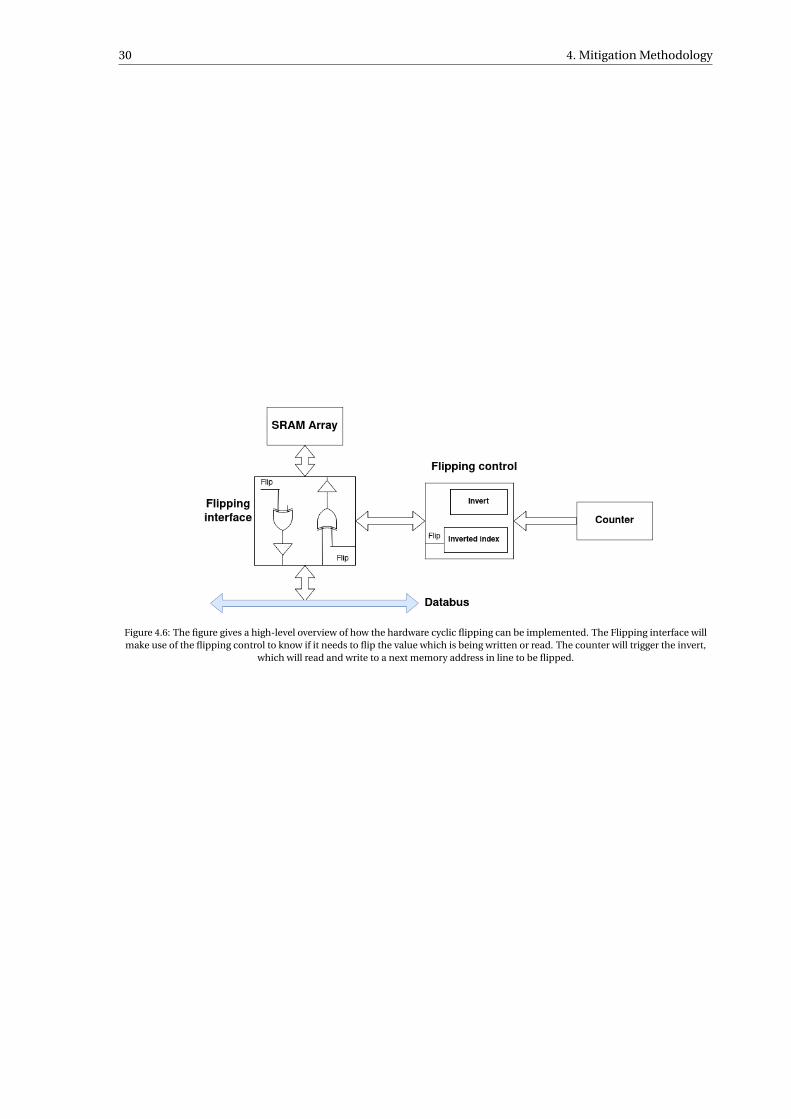
30 4. Mitigation Methodology
Figure 4.6: The figure gives a high-level overview of how the hardware cyclic flipping can be implemented. The Flipping interface willmake use of the flipping control to know if it needs to flip the value which is being written or read. The counter will trigger the invert,
which will read and write to a next memory address in line to be flipped.
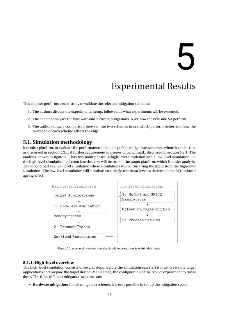
5Experimental Results
This chapter performs a case-study to validate the selected mitigation schemes:
1. The authors discuss the experimental setup, followed by what experiments will be executed.
2. The chapter analyses the hardware and software mitigations to see how the cells and SA perform.
3. The authors draw a comparison between the two schemes to see which perform better and how theoverhead of each scheme affects the chip.
5.1. Simulation methodologyIt needs a platform, to evaluate the performance and quality of the mitigations scheme’s, where it can be run,as discussed in section 5.2.1. A further requirement is a series of benchmark; discussed in section 5.2.1. Theanalysis, shown in figure 5.1, has two main phases: a high-level simulation and a low-level simulation. Inthe high-level simulation, different benchmarks will be run on the target platform, which is under analysis.The second part is a low-level simulation where simulations will be run using the input from the high-levelsimulation. The low-level simulation will simulate on a single transistor level to determine the BTI-inducedageing effect.
High level Simulation
Target Applications
1: Modelsim simulation
Memory traces
2: Process Traces
Workload Abstraction
Low level Simulation
1: Matlab and SPICESimulations
Offset voltages and SNM
2: Process results
Figure 5.1: A general overview how the simulation setup works within this thesis.
5.1.1. High-level overviewThe high-level simulation consists of several steps. Before the simulation can start it must create the targetapplications and prepare the target device. At this stage, the configuration of the type of experiment to run isdone. The three different mitigation schemes are:
• Hardware mitigation: In this mitigation scheme, it is only possible to set up the mitigation speed.
31

32 5. Experimental Results
• Software mitigation: In this mitigation scheme, it is possible to configure the chunk size and the inter-val at which the co-routine is run.
• Software mitigation with added idle time: In this mitigation scheme, it is chosen to fix the interval andchunk size during the run-time of the benchmarks. It will only allow configuration of the overhead,which the mitigation scheme can use, after and benchmark finishes.
After the configuration is set up, the first simulation, (i.e. the Modelsim simulation) can run. It will returnas memory traces consisting of all the read and write operations to the memory. The next stage will processthe memory traces to create an analysis to find the memory cells with the most static stress, and the mostextreme duty factor. Next to the cell analysis, the sense amplifier is carefully analysed, and the bit distributionis calculated for each bit which is converted to duty factors using the code supplied by IMEC. The workloadabstraction uses the calculated duty factors, which provide input for the low-level simulation phase.
5.1.2. Low-level simulationThe high-level simulation phase supplies the inputs for the low-level simulation phase. Two different work-load abstractions have been created: one for the memory cell and one for the sense amplifier. For the memorycells, the BTI-induced ageing will be analysed in MATLAB, after which the SNM will be simulated in SPICE. AMonto-Carlo simulation analyses the sense amplifier directly in SPICE, to determine the offset voltage of thesense amplifier. After calculating the offset voltage and the SNM, the researchers can process the results tosee which configuration yields the best results for the given circumstances.
5.2. Performed experimentsThis section will explain the setup of the experiments and the different effects of BTI-induced ageing in thememory cells.
5.2.1. SetupThe setup of the experiments requires several different components:
• A platform on which the benchmark and mitigation scheme can run (i.e. PULPINO).• Benchmarks which are used to create memory traces.
Benchmark platformAfter introducing the overview of the simulation, it is now required to introduce the platform, which is usedto run the benchmarks on PULPINO. It is required to have an implementation target device. For this, thePULPINO is used the details of the platform and implementation are discussed in [92].
Figure 5.2: Schematic overview of the PULPINO RISCY core. Image from [6]
The PULPINO comes with instructions and a separate dataram, each being 32 KiB consisting of a wordsize of 32 bit resulting into 8192 words. The processor is a four-stage pipeline, and its memory map is shown infigure A.1. The PULPINO reassembles a microcontroller architecture. Within microcontrollers, the programis stored in flash memory. Flash memories are not subjected to ageing as with that the data RAM.
BenchmarksAs the PULPINO core has only 32 KiB amount of RAM available it can only run a limit set of benchmarks. Theavailable benchmarks are shown in table 5.1, and a few key metrics are given. Next, an analysis is made of thechunk of the memory cells are subjected to long static stress. For all benchmarks, except the FFT-benchmark,all memory addresses have cells with static values for the complete benchmark.
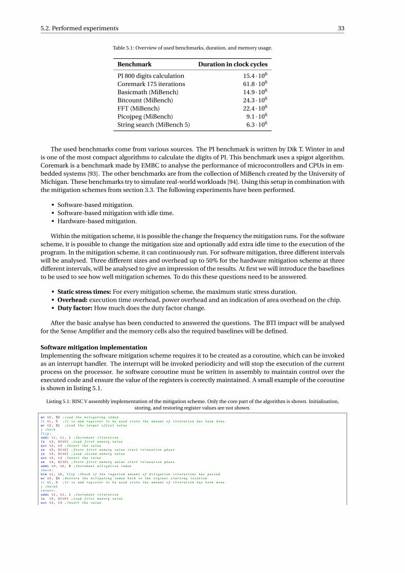
5.2. Performed experiments 33
Table 5.1: Overview of used benchmarks, duration, and memory usage.
Benchmark Duration in clock cycles
PI 800 digits calculation 15.4 ·106
Coremark 175 iterations 61.8 ·106
Basicmath (MiBench) 14.9 ·106
Bitcount (MiBench) 24.3 ·106
FFT (MiBench) 22.4 ·106
Picojpeg (MiBench) 9.1 ·106
String search (MiBench 5) 6.3 ·106
The used benchmarks come from various sources. The PI benchmark is written by Dik T. Winter in andis one of the most compact algorithms to calculate the digits of PI. This benchmark uses a spigot algorithm.Coremark is a benchmark made by EMBC to analyse the performance of microcontrollers and CPUs in em-bedded systems [93]. The other benchmarks are from the collection of MiBench created by the University ofMichigan. These benchmarks try to simulate real-world workloads [94]. Using this setup in combination withthe mitigation schemes from section 3.3. The following experiments have been performed.
• Software-based mitigation.• Software-based mitigation with idle time.• Hardware-based mitigation.
Within the mitigation scheme, it is possible the change the frequency the mitigation runs. For the softwarescheme, it is possible to change the mitigation size and optionally add extra idle time to the execution of theprogram. In the mitigation scheme, it can continuously run. For software mitigation, three different intervalswill be analysed. Three different sizes and overhead up to 50% for the hardware mitigation scheme at threedifferent intervals, will be analysed to give an impression of the results. At first we will introduce the baselinesto be used to see how well mitigation schemes. To do this these questions need to be answered.
• Static stress times: For every mitigation scheme, the maximum static stress duration.• Overhead: execution time overhead, power overhead and an indication of area overhead on the chip.• Duty factor: How much does the duty factor change.
After the basic analyse has been conducted to answered the questions. The BTI impact will be analysedfor the Sense Amplifier and the memory cells also the required baselines will be defined.
Software mitigation implementationImplementing the software mitigation scheme requires it to be created as a coroutine, which can be invokedas an interrupt handler. The interrupt will be invoked periodicity and will stop the execution of the currentprocess on the processor. he software coroutine must be written in assembly to maintain control over theexecuted code and ensure the value of the registers is correctly maintained. A small example of the coroutineis shown in listing 5.1.
Listing 5.1: RISC V assembly implementation of the mitigation scheme. Only the core part of the algorithm is shown. Initialisation,storing, and restoring register values are not shown.
mv t0 , %0 ;Load the mitigating indexli t1 , 0 ;t1 is and register to be used store the amount of itteration has been done.mv t2 , %1 ;Load the target offset valuej checkflip:addi t1, t1, 1 ;Increment itterationlw t3, 0(t0) ;Load first memory valuenot t3, t3 ;Invert the valuesw t3, 0(t0) ;Store first memory value start relaxation phaselw t3, 0(t0) ;Load second memory valuenot t3, t3 ;Invert the valuesw t3, 0(t0) ;Store first memory value start relaxation phaseaddi t0, t0, 8 ;Increment mitigation indexcheck:ble t1, t2, flip ;Check if the required amount of mitigation itterations has passedmv t0 , %0 ;Restore the mitigating index back to the orginal starting locationli t1 , 0 ;t1 is and register to be used store the amount of itteration has been done.j check2revert:addi t1, t1, 1 ;Increment itterationlw t3, 0(t0) ;Load first memory valuenot t3, t3 ;Invert the value

34 5. Experimental Results
sw t3, 0(t0) ;Store first memory value start relaxation phaselw t3, 0(t0) ;Load second memory valuenot t3, t3 ;Invert the valuesw t3, 0(t0) ;Store first memory value start relaxation phaseaddi t0, t0, 8 ;Increment mitigation indexcheck2:ble t1, t2, revert
5.2.2. BTI effect in the cellFor the memory cell, BTI effects will be analysed by the usage of the cell shown in figure 2.3. It consists of sixtransistors; four are subjected to static stress. The transistors M1 and M2 store the inverted value in the cell,while the transistors M3 and M4 store the normal value. Due to this balance in the cell bit values, zero andone will each create static stress and unbalancing the ageing in the cell. The transistors M5 and M6 are usedto read or write values from and to the cell.
The BTI effect in the cell will degrade the SNM. The degrading of the cell is the strongest if the cell storesstatic values. For the extreme cases of zero or one-bit,value, stored for three years in the cell, the graph ofthe ageing of the transistors is shown in figure 5.3. This is also compared to the ideal case where the dutyfactor of the transistors M1 up to M4 is 0.5. When the memory cell is ageing perfectly balanced the SNM doesnot change, whereas when the duty factor reaches the extreme values, the BTI effect accelerates. Using thecalculated voltage shift in the transistors the ageing effect in the memory cell can be calculated using SPICEin Cadence. Table 5.2 shows the different cases to illustrate the effect the duty factors have on the ageing ofan SRAM-cell.
0 1 2 3 4 5 6 7 8 9 10
Time in s 107
-85
-80
-75
-70
-65
-60
-55
-50
Delta V
th in m
V
Simulation of transistors with different duty factors after 3 years of ageing at 125 degrees
Transistor with a duty factor 1
Transistor with a duty factor 0.9
Transistor with a duty factor 0.5
Figure 5.3: Comparing different duty factors on the transistors. If the duty factor is slightly reduced from 1.0 to 0.9, it has a relativelylarger impact than when changing the duty factor from 0.9 to 0.5.
Table 5.2: Overview of different static stress durations depending on the running mitigation. Comparing the different mitigationscheme size to the interval at which they are run.
Duty factor static noise margin
No ageing 354 mV0.0 328 mV0.1 350 mV0.5 355 mV0.9 350 mV1.0 328 mV
5.2.3. BTI effect in the Sense AmplifierAnalysing the BTI in the SA is much more difficult as it is required to know the distribution of bits beingread and the active time. The distribution of bits and active time will be calculated by running the differentbenchmarks.To analyse the SA Monto Carlo simulation is used which has been provided by IMEC. A Python script has been

5.3. Software Mitigation Results 35
created to analyse the results from the simulation. The Monto Carlo simulation consists of 2000 iterations.For the SA it is only possible to define the start value of the offset voltage which is in ideal cases 0 mV.
5.3. Software Mitigation ResultsAt first the results of software mitigation are discussed. The implemented algorithm is the multiple cell mit-igation, resulting in the lowest execution overhead compared to the other implementation, as discussed insection 4.4.
A python code has been designed to create the different routines variating the sizes and speed of thesoftware mitigation, which will craft the assembly code to inject into the benchmarks.
5.3.1. Cell performanceThe performance will be measured and shown for each benchmark looking at the memory cells and senseamplifier. Figures 5.4 to 5.6 shows the SNM degradation of the memory cells, running different mitigationscheme configuration, with and without mitigation. The observations are as follow:
• The SNM degradation is not application dependent. The requirement is that the benchmark simulationis long enough to complete full mitigation of the memory.
• The degradation of the SNM is reduced significantly, when adding a mitigation scheme, allowing themitigation to have a higher overhead with a lower return on investment.
• The mitigation scheme reduces the degradation of the SNM significantly (up to 2.5x).
Static noise margin degradation
Basicmath Bitcount Coremark FFT JPEG Pi String Search0
5
10
15
20
25
30
Vo
lta
ge
(m
V)
Baseline
With mitgation - 512 cells - 12e5cycles
With mitgation - 512 cells - 6e5cycles
With mitgation - 512 cells - 3e5cycles
Figure 5.4: The degradation of the SNM running different benchmarks with and without mitigation scheme. The software scheme willrelax 512 memory cells at different intervals. The experiment is run at 125 C for three years.
Table 5.3 shows that the cell performance is application-independent, as derived from the graph to com-pare the Vth shift. When looking at the degradation of the SNM at a block size of 2048 and an interval at1.2×106 cycles and to the 512 block size and an interval of 3×10⁵ cycles. The latter option has a biggerdegradation while the overhead of both mitigation schemes is the same. The memory cell should have aslightly longer relaxation and static stress than a shorter relaxation and duration when stress is present.
Table 5.3: Overview SNM of cells with different mitigation scheme settings running. The longer and the faster the mitigation is run, thebetter the mitigation scheme performs. It can also be seen that reduction of the length of static stress has a smaller impact on the SNM
than running the mitigation scheme longer.
Block size 1.2×10⁶ 6.0×10⁵ 3.0×10⁵
512 17.4 mV 16.5 mV 15.4 mV1024 15.1 mV 14.7 mV 13.2 mV2048 13.3 mV 12.0 mV 10.9 mV

36 5. Experimental Results
Static noise margin degradation
Basicmath Bitcount Coremark FFT JPEG Pi String Search0
5
10
15
20
25
30
Vo
lta
ge
(m
V)
Baseline
With mitgation - 1024 cells - 12e5 cycles
With mitgation - 1024 cells - 6e5cycles
With mitgation - 1024 cells - 3e5cycles
Figure 5.5: The degradation of the SNM running different benchmarks with and without mitigation scheme. The software scheme willrelax 1024 memory cells at different intervals. The experiment is run at 125 C for three years.
Static noise margin degradation
Basicmath Bitcount Coremark FFT JPEG Pi String Search0
5
10
15
20
25
30
Vo
lta
ge
(m
V)
Baseline
With mitgation - 2048 cells - 12e5cycles - 1.3%
With mitgation - 2048 cells - 6e5cycles - 2.7%
With mitgation - 2048 cells - 3e5cycles - 5.5%
Figure 5.6: The degradation of the SNM running different benchmarks with and without mitigation scheme. The software scheme willrelax 2048 memory cells at different intervals. The experiment is run at 125 C for three years.
Figure 5.7 shows the SNM degradation of the memory cells running the software mitigation differently,with added idle time. The SNM is shown with and without mitigation. The following can be observed fromthe figure:
• The SNM degradation is not application dependent. The requirement is that the benchmark simulationis long enough to complete full mitigation of the memory.
• The degradation of the SNM is reduced significantly, when adding a mitigation scheme, allowing themitigation to have a higher overhead results in a lower return on investment.
• The mitigation scheme reduces the degradation of the SNM (up to 2.5x)• Adding idle time into the simulation reduces the ageing of the memory cells.
After analysing the mitigation scheme without injecting idle time, the next part will analyse the SNMdegradation if idle time is used to mitigate static stress in memories. Adding idle time to the simulation of themitigation scheme reduces of the degradation on the SNM as shown in table 5.4. The biggest improvementis when adding a slight overhead into the simulation. This is expected, and the more overhead that is added,the better the result.

5.3. Software Mitigation Results 37
Static noise margin degradation
Basicmath Bitcount Coremark FFT JPEG Pi String Search0
5
10
15
20
25
30
Vo
lta
ge
(m
V)
Baseline
With mitgation - 1024 cells - 12e5 cycles and 10% idle time
With mitgation - 1024 cells - 12e5 cycles and 20% idle time
With mitgation - 1024 cells - 12e5 cycles and 30% idle time
With mitgation - 1024 cells - 12e5 cycles and 50% idle time
Figure 5.7: The degradation of the SNM running different benchmarks with and without mitigation scheme. The software scheme willrelax 1024 memory cells at a fixed interval and add a varying amount of idle time. The experiment is run at 125 C for three years.
Table 5.4: Overview SNM degradation of the cells after adding idle time to the simulation of the benchmarks.
Idle time overhead SNM offset voltage
10% 4.9 mV20% 3.6 mV30% 2.8 mV50% 1.9 mV
5.3.2. Sense amplifierFor the sense amplifier, it is not possible to group the results as for the cells due to different bit distribution,and sense amplifier activation between every benchmark.
In figures 5.8 to 5.10 the offset voltage sense amplifier is plotted. The different software mitigations config-uration has been run. The offset voltage is shown with and without mitigation. The following can be observedfrom the figure:
• The offset voltage of the sense amplifier is application-dependent. Each benchmark has an optimalmitigation scheme to reduce the offset voltage.
• The offset voltage can increase if the amount of memory operation increases to much and cause morestresses in the sense amplifier. Across the run benchmarks, the overall offset voltage improves over theworst benchmark.
• The mitigation scheme can reduce the offset voltage with nearly 50%.
Figures 5.8 to 5.10 show the results of the different software mitigation schemes without the simulationof idle time. The benchmark, JPEG, can even have a higher degradation as compared to running no mitiga-tion scheme. The worst-case performance significantly improves over the different benchmarks. While thebenchmark, Coremark, defines the result.
Figure 5.11 shows the results from adding idle time to the mitigation scheme. There is a balance in themitigation scheme and the usage of the sense amplifier:
• The offset voltage of the sense amplifier is application dependent. Each benchmark has an optimalmitigation scheme to reduce the offset voltage.
• The offset voltage can increase if the amount of memory operation increases, which causes more stressesin the sense amplifier. In all the run benchmarks, the overall offset voltage always improves over theworst possible benchmark.
• Using idle time to mitigate the offset voltage increase, reduces the performances.

38 5. Experimental Results
Offset voltage for the sense amplifier
Basicmath Bitcount Coremark FFT JPEG Pi String Search45
50
55
60
65
Off
se
t vo
lta
ge
(m
V)
Baseline
With mitgation - 512 cells - 12e5cycles
With mitgation - 512 cells - 6e5cycles
With mitgation - 512 cells - 3e5cycles
Figure 5.8: The degradation of the sense amplifier running different benchmarks with and without mitigation scheme. The softwarescheme will relax 512 cells at different intervals. The faster the mitigation scheme runs, the more balanced the sense amplifier will be. Itwill also be used more. The more usage of the sense amplifier can result in extra degradation of the offset voltage spec. The experiment
is run at 125 C for three years.
Offset voltage for the sense amplifier
Basicmath Bitcount Coremark FFT JPEG Pi String Search45
50
55
60
65
Off
se
t vo
lta
ge
(m
V)
Baseline
With mitgation - 1024 cells - 12e5 cycles
With mitgation - 1024 cells - 6e5cycles
With mitgation - 1024 cells - 3e5cycles
Figure 5.9: The degradation of the sense amplifier running different benchmarks with and without mitigation scheme. The softwarescheme will relax 1024 cells at different intervals. The faster the mitigation scheme runs, the more balanced the sense amplifier will be.
It will also be used more. The more usage of the sense amplifier can result into extra degradation of the offset voltage spec. Theexperiment is run at 125 C for three years.
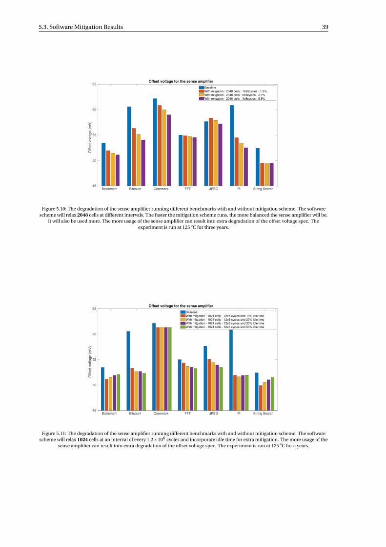
5.3. Software Mitigation Results 39
Offset voltage for the sense amplifier
Basicmath Bitcount Coremark FFT JPEG Pi String Search45
50
55
60
65
Off
se
t vo
lta
ge
(m
V)
Baseline
With mitgation - 2048 cells - 12e5cycles - 1.3%
With mitgation - 2048 cells - 6e5cycles - 2.7%
With mitgation - 2048 cells - 3e5cycles - 5.5%
Figure 5.10: The degradation of the sense amplifier running different benchmarks with and without mitigation scheme. The softwarescheme will relax 2048 cells at different intervals. The faster the mitigation scheme runs, the more balanced the sense amplifier will be.
It will also be used more. The more usage of the sense amplifier can result into extra degradation of the offset voltage spec. Theexperiment is run at 125 C for three years.
Offset voltage for the sense amplifier
Basicmath Bitcount Coremark FFT JPEG Pi String Search45
50
55
60
65
Off
se
t vo
lta
ge
(m
V)
Baseline
With mitgation - 1024 cells - 12e5 cycles and 10% idle time
With mitgation - 1024 cells - 12e5 cycles and 20% idle time
With mitgation - 1024 cells - 12e5 cycles and 30% idle time
With mitgation - 1024 cells - 12e5 cycles and 50% idle time
Figure 5.11: The degradation of the sense amplifier running different benchmarks with and without mitigation scheme. The softwarescheme will relax 1024 cells at an interval of every 1.2×10⁶ cycles and incorporate idle time for extra mitigation. The more usage of the
sense amplifier can result into extra degradation of the offset voltage spec. The experiment is run at 125 C for a years.

40 5. Experimental Results
5.4. Hardware Mitigation ResultsThe software results have been discussed. Next step is to look at the hardware implementation. The chosenalgorithm is the cyclic flipping, as shown in section 4.5. This algorithm will have the best mitigation per-formance. The implementation is done in Verilog and will allow configuring at which interval the hardwaremitigation will run.
5.4.1. Cell performanceThe hardware mitigation scheme will make sure the average duty factor of every cell is balanced at the valueof 0.5. The average duty factor might stay higher if the hardware mitigation scheme does not run fast enoughto complete a cyclic pass through the memory within the duration of the benchmark. In figure 5.12 the SNMis shown for the different mitigation scheme settings. Some benchmarks have outliers because they are tooshort to run a balanced mitigation scheme using the hardware mitigation scheme settings. From this figure,the following observation have been made:
• The SNM degradation is slightly application dependent. The requirement is that the benchmark simu-lation is long enough to complete full mitigation of the memory. The other requirement is that memoryvalues should not be accidentally moved to longer static stress due to flipping of the value.
• The degradation of the SNM is reduced significantly, when adding a mitigation scheme allowing themitigation to have a higher overhead with a lower return on investment.
• The mitigation scheme reduces the degradation of the SNM (up to 45x).
Static noise margin degradation
Basicmath Bitcount Coremark FFT JPEG Pi String Search0
5
10
15
20
25
30
Vo
lta
ge
(m
V)
Baseline
Hardware flip one cell - 2047 cycles
Hardware flip one cell - 1024 cycles
Hardware flip one cell - 511 cycles
Hardware flip one cell - 255 cycles
Figure 5.12: The degradation of the memory cell running different benchmarks with and without mitigation scheme. Hardwaremitigation allows for better balancing if the benchmark is long enough. The ageing effect due to BTI nearly disappears. The experiment
is run at 125 C for three years.
5.4.2. Sense amplifier performanceThere is a significant difference depending on the benchmark: how many read, write operation, bit distribu-tion. This difference is less with hardware mitigation as shown in figure 5.13:
• The offset voltage of the sense amplifier is application dependent. Each benchmark has an optimalmitigation scheme to reduce the offset voltage.
• The offset voltage can increase if the amount of memory operation increases slightly in all the runbenchmarks. The overall offset voltage always improves over the worst possible benchmark.
• The mitigation scheme can reduce the offset voltage with nearly 67%.
The hardware mitigation scheme balances the sense amplifier much better compared to the softwaremitigation scheme where the result still is very much dependant on the running benchmark.
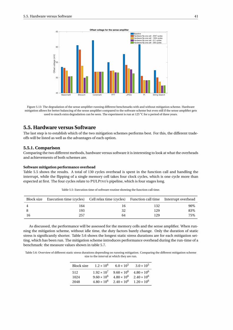
5.5. Hardware versus Software 41
Offset voltage for the sense amplifier
Basicmath Bitcount Coremark FFT JPEG Pi String Search45
50
55
60
65
Off
se
t vo
lta
ge
(m
V)
Baseline
Hardware flip one cell - 2047 cycles
Hardware flip one cell - 1024 cycles
Hardware flip one cell - 511 cycles
Hardware flip one cell - 255 cycles
Figure 5.13: The degradation of the sense amplifier running different benchmarks with and without mitigation scheme. Hardwaremitigation allows for better balancing of the sense amplifier compared to the software scheme but even still if the sense amplifier gets
used to much extra degradation can be seen. The experiment is run at 125 C for a period of three years.
5.5. Hardware versus SoftwareThe last step is to establish which of the two mitigation schemes performs best. For this, the different trade-offs will be listed as well as the advantages of each option.
5.5.1. ComparisonComparing the two different methods, hardware versus software it is interesting to look at what the overheadsand achievements of both schemes are.
Software mitigation performance overheadTable 5.5 shows the results. A total of 130 cycles overhead is spent in the function call and handling theinterrupt, while the flipping of a single memory cell takes four clock cycles, which is one cycle more thanexpected at first. The four cycles relate to PULPINO’s pipeline, which is four stages long.
Table 5.5: Execution time of software routine showing the function call time.
Block size Execution time (cycles) Cell relax time (cycles) Function call time Interrupt overhead
4 164 16 132 90%8 193 32 129 83%16 257 64 129 75%
As discussed, the performance will be assessed for the memory cells and the sense amplifier. When run-ning the mitigation scheme, without idle time, the duty factors barely change. Only the duration of staticstress is significantly shorter. Table 5.6 shows the longest static stress durations are for each mitigation set-ting, which has been run. The mitigation scheme introduces performance overhead during the run-time of abenchmark: the measure values shown in table 5.7.
Table 5.6: Overview of different static stress durations depending on running mitigation. Comparing the different mitigation schemesize to the interval at which they are run.
Block size 1.2×10⁶ 6.0×10⁵ 3.0×10⁵
512 1.92×10⁷ 9.60×10⁶ 4.80×10⁶
1024 9.60×10⁶ 4.80×10⁶ 2.40×10⁶
2048 4.80×10⁶ 2.40×10⁶ 1.20×10⁶

42 5. Experimental Results
Table 5.7: Overview of different static stress durations depending on running mitigation. Comparing the different mitigation schemesize to the interval at which they are run.
Block size 1.2×10⁶ 6.0×10⁵ 3.0×10⁵
512 0.4% 0.7% 1.4%1024 0.7% 1.4% 2.8%2048 1.4% 2.8% 5.5%
When adding the idle time, which is a fraction of the execution time of the benchmark, will result in asignificant change of the duty factor in table 5.8.
Table 5.8: Overview of different of the duty factor which can be found in the cells depending on the different amounts of available idletime.
Overhead Low duty factor High duty factor
10% 0.05 0.9520% 0.08 0.9230% 0.11 0.8940% 0.14 0.8650% 0.17 0.83
After analysing the mitigation scheme impact, the next step is to inspect the effect on the BTI-ageing.
Hardware mitigation performance overheadThe hardware implementation is in Verilog and will only use the memory when the IC does not require accessto the memory. The hardware implementation will, therefore, not add any overhead in the form of executiontime. The overhead will consist of extra hardware, which will be required, and extra usage of the memory,thus, more power usage and a larger chip.
Looking at how the static stress duration is handled within the hardware mitigation, this study does thesame analysis within the software mitigation scheme. These results are shown in table 5.9.
Table 5.9: Overview of different static stress durations depending on running mitigation. Comparing the different intervals at which thehardware mitigation can run.
Block size Static stress duration in cycles
255 2.09×10⁶
511 4.19×10⁶
1023 8.38×10⁶
2047 1.68×10⁷
5.5.2. Memory overheadTable 5.10 shows the memory-overhead usage for the different mitigation scheme, which has been anal-ysed. The hardware mitigation scheme requires a lot less memory usage compared to the software mitigationscheme.
5.5.3. ConclusionSoftware mitigation scheme introduces execution overhead and memory usages, whereas the hardware mit-igation scheme introduces memory usage overhead and requires extra hardware. Table 5.11 highlights keypoints of the effect of hardware and software mitigation scheme, which summarise the implementation. Thehardware mitigation scheme brings greater improvement compared to the software mitigation scheme, as itchanges the average duty factor.

5.5. Hardware versus Software 43
Table 5.10: Comparing the memory overhead of the different scheme which has been created and run.
Benchmark Memory overhead usage compared to the baseline
Hardware mitigation - 255 cycles 101.6%Hardware mitigation - 511 cycles 101%Hardware mitigation - 1024 cycles 100.5%Hardware mitigation - 2047 cycles 100.2%Software mitigation - 1024 cells - 12e5 cycles 101.7%Software mitigation - 1024 cells - 3e5cycles 107%Software mitigation - 1024 cells - 6e5cycles 103.5%Software mitigation - 512 cells - 12e5cycles 100.9%Software mitigation - 512 cells - 6e5cycles 101.8%Software mitigation - 512 cells - 3e5cycles 103.5%Software mitigation - 2048 cells - 12e5cycles 103.4%Software mitigation - 2048 cells - 6e5cycles 106.9%Software mitigation - 2048 cells - 3e5cycles 113.8%
Table 5.11: An overview of the different impacts of the hardware and software mitigation scheme on the memory and IC.
Item Hardware Software
Execution overhead No impact on execution time Increases execution timeMemory usages Slight increase Increase with up to 15%Idle time - Can utilise idle timeImpact on duty factor Average moves to 0.5 Duty factor does not changeHardware overhead Requires extra transistors NoneImplementation During chip design Can be implemented afterwardsSNM improvementOffset voltage improvement


6Conclusion
6.1. ConclusionThis thesis has shown that mitigating BTI induced ageing in SRAM is possible by adding software coroutines.Both the memory cells and the Sense Amplifier saw a significant reduction in BTI-induced ageing at verylow overhead. The memory cell ageing was reduced with up to 40% at a run-time overhead of only 1.4%. Inaddition, the degradation of the SA was reduced by up to 50%. This reduced degradation leads to a morereliable memory and an increased lifetime. Moreover, when adding idle time to the simulated workload,software mitigation scheme could make a significant improvement.
In addition, this thesis showed that the implemented hardware mitigation scheme is more efficient com-pared to the software mitigation scheme. This is due to the fact that the hardware mitigation scheme can bet-ter balance the overall duty cycles of the memory cell to 50%. As a result, the hardware mitigation scheme alsoyields a much higher reduction of BTI-induced ageing at the cost of adding extra hardware to the memory.Nevertheless, software mitigation schemes can be easily added to the compilers. Hence, the software-basedapproach can even be added to existing hardware without requiring modifications. This addition will extendthe lifetime of the chip at the costs of extending the required run-time of a program. Additionally, softwaremitigation could also make use of run-time information, while this would be much harder to implement inhardware. Hence, both software mitigation and hardware mitigation have their merits. For example, thesoftware-based scheme is interesting for systems that require a low area, while the hardware-based schemeis interesting when this restriction is not present. The usage of BIST for mitigation of BTI-induced ageingwithin the memories is not feasible, as the best mitigation scheme will flip the cells values compared to thevalue they are storing.
6.2. Future workThe work presented two different mitigation schemes against the effect of BTI-induced ageing. The researchwithin the thesis can be extended by looking at:
• Circuit modelThe suggested mitigation scheme can be applied to a newer, more modern SRAM design. The the-sis used a 14 nm. It would be interesting to find out how much of an improvement these mitigationschemes can provide on a smaller technology node. This is due to the fact that smaller technologynodes are more affected by ageing.
• SensingAdding sensors within the memory could allow for smarter mitigation schemes. The state of the artshowed that the results of this are not promising. An in-depth comparison could be made betweenmitigation schemes with and without sensors. Sensors could be combined with AI to be able to makesmarter sensors.
• Different platformsWith this thesis, the work focused on the PULPINO, which has a RISC-V architecture. In future re-
45

46 6. Conclusion
search, different platforms could be analysed with different architects and allowing more advancedbenchmarks.
• Improve ageing modelThis research could also be extended with a more accurate ageing model. For example, add HCI, TDDB,and RTN to the ageing model. Furthermore, if a complete memory design is available EM degradationcould be included.
• Extending the analysisThis research could be extended in depth of the analysed components. First of all, the effect on morememory components can be investigated, such as the address decoder and timing circuit. It is expectedthat both the proposed software- and hardware-based mitigation schemes will reduce the ageing of theaddress decoder. This is due to the fact that they both ensure all memory addresses are traversed and,thus, static stresses will be reduced in the address decoder. This is already briefly demonstrated in [95].Second, future work could also analyse more metrics, such as the write and hold SNM of the memorycell. This work analysed the read SNM, as it is the most critical metric. However, for a reliable designany metric should stay within its specifications even under ageing.

APULPINO
47
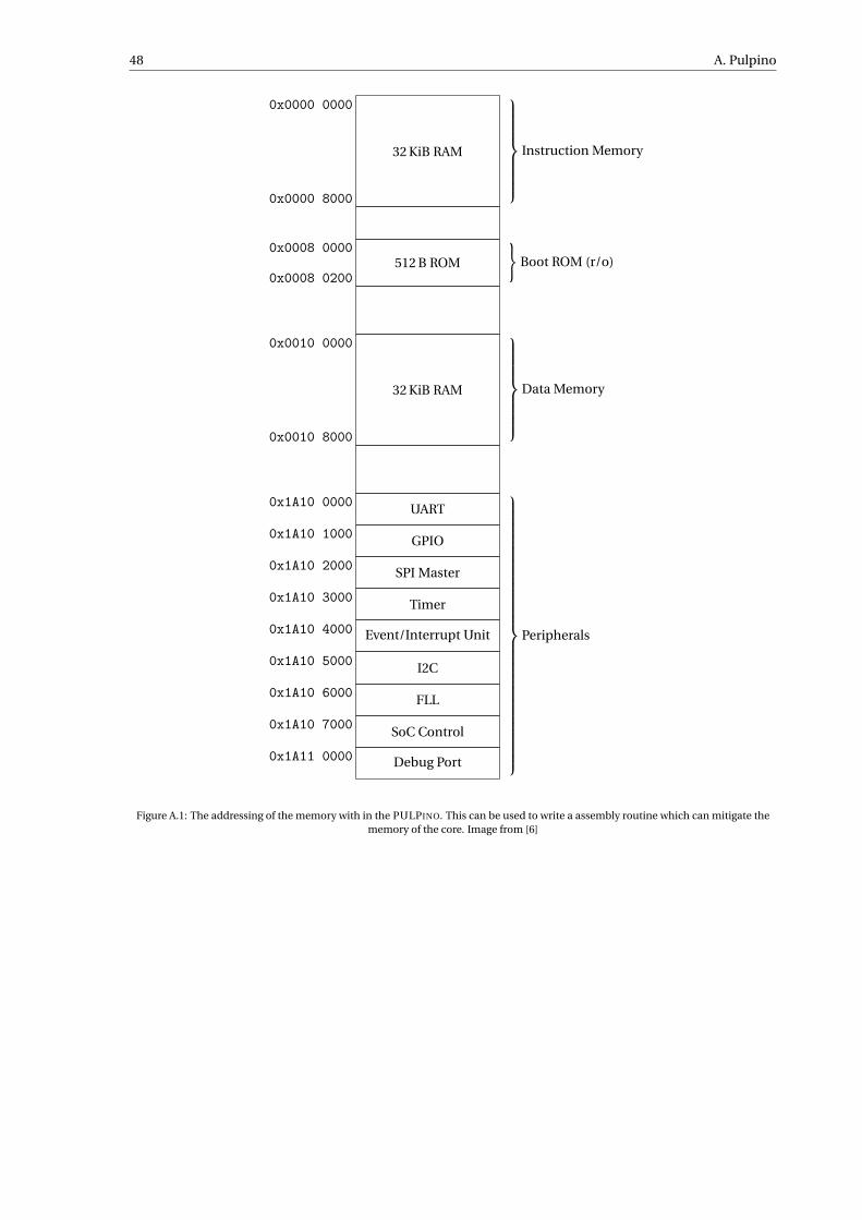
48 A. Pulpino
0x0000 0000
0x0000 8000
32 KiB RAM
Instruction Memory
0x0008 0000
0x0008 0200512 B ROM
Boot ROM (r/o)
0x0010 0000
0x0010 8000
32 KiB RAM
Data Memory
0x1A10 0000 UART
0x1A10 1000 GPIO
0x1A10 2000 SPI Master
0x1A10 3000 Timer
0x1A10 4000 Event/Interrupt Unit
0x1A10 5000 I2C
0x1A10 6000 FLL
0x1A10 7000SoC Control
0x1A11 0000 Debug Port
Peripherals
Figure A.1: The addressing of the memory with in the PULPINO. This can be used to write a assembly routine which can mitigate thememory of the core. Image from [6]
Bibliography
[1] A. Nowak, “Opportunities and choice in a new vector era,” Journal of Physics: Conference Series, vol. 523, no. 1, 2014.
[2] I. Agbo, M. Taouil, S. Hamdioui, H. Kukner, P. Weckx, P. Raghavan, and F. Catthoor, “Integral impact of BTI and voltagetemperature variation on SRAM sense amplifier,” Proceedings of the IEEE VLSI Test Symposium, vol. 2015-January,pp. 1–6, 2015.
[3] D. Kraak, M. Taouil, I. Agbo, S. Hamdioui, P. Weckx, S. Cosemans, and F. Catthoor, “Parametric and functional degra-dation analysis of complete 14-nm finfet sram,” IEEE Transactions on Very Large Scale Integration (VLSI) Systems,vol. 27, no. 6, pp. 1308–1321, June 2019.
[4] A. Campos-Cruz, G. Espinosa-Flores-Verdad, A. Torres-Jacome, and E. Tlelo-Cuautle, “On the Prediction of theThreshold Voltage Degradation in CMOS Technology Due to Bias-Temperature Instability,” Electronics, vol. 7,no. 12, p. 427, dec 2018. [Online]. Available: http://www.mdpi.com/2079-9292/7/12/427
[5] K. N. Quader, C. Li, R. Tu, E. Rosenbaum, P. Ko, and C. Hu, “A new approach for simulation of circuit degradationdue to hot-electron damage in NMOSFETs,” Technical Digest - International Electron Devices Meeting, IEDM, vol.1991-Janua, no. 7, pp. 337–340, 1991.
[6] A. Traber and M. Gautschi, PULPino: Datasheet Imperio: The first PULPino ASIC, 2017.
[7] M. T. Bohr and I. A. Young, “CMOS Scaling Trends and beyond,” IEEE Micro, vol. 37, no. 6, pp. 20–29, 2017.
[8] S. Borkar, “Designing reliable systems from unreliable components: The challenges of transistor variability anddegradation,” IEEE Micro, vol. 25, no. 6, pp. 10–16, nov 2005. [Online]. Available: http://ieeexplore.ieee.org/document/1566551/
[9] R. Aitken, E. H. Cannon, M. Pant, and M. B. Tahoori, “Resiliency challenges in sub-10nm technologies,” Proceedingsof the IEEE VLSI Test Symposium, vol. 2015-January, pp. 1–4, 2015.
[10] E. Suhir, “Aging-related failure rate obtained from bathtub curve data,” in 2015 IEEE Aerospace Conference, 2015, pp.1–8.
[11] H. F. Dadgour and K. Banerjee, “A built-in aging detection and compensation technique for improving reliability ofnanoscale cmos designs,” 2010, pp. 822–825.
[12] K. Jeong, A. B. Kahng, and K. Samadi, “Impact of guardband reduction on design outcomes: A quantitative ap-proach,” pp. 552–565, 2009.
[13] P. Gupta, Y. Agarwal, L. Dolecek, N. Dutt, R. K. Gupta, R. Kumar, S. Mitra, A. Nicolau, T. S. Rosing, M. B. Srivastava,S. Swanson, and D. Sylvester, “Underdesigned and opportunistic computing in presence of hardware variability,”IEEE Transactions on Computer-Aided Design of Integrated Circuits and Systems, vol. 32, no. 1, pp. 8–23, 2013.
[14] K. Wu and D. Marculescu, “Aging-aware timing analysis and optimization considering path sensitization,” in 2011Design, Automation Test in Europe, March 2011, pp. 1–6.
[15] M. Ebrahimi, F. Oboril, S. Kiamehr, and M. B. Tahoori, “Aging-aware logic synthesis,” in Proceedings of theInternational Conference on Computer-Aided Design, ser. ICCAD ’13. Piscataway, NJ, USA: IEEE Press, 2013, pp.61–68. [Online]. Available: http://dl.acm.org/citation.cfm?id=2561828.2561840
[16] S. Kiamehr, F. Firouzi, M. Ebrahimi, and M. B. Tahoori, “Aging-aware standard cell library design,” Proceedings -Design, Automation and Test in Europe, DATE, vol. 3, pp. 1–4, 2014.
[17] N. Khoshavi, R. A. Ashraf, R. F. DeMara, S. Kiamehr, F. Oboril, and M. B. Tahoori, “Contemporary cmos agingmitigation techniques: Survey, taxonomy, and methods,” Integration, vol. 59, pp. 10 – 22, 2017. [Online]. Available:http://www.sciencedirect.com/science/article/pii/S0167926017301876
[18] M. Sipser, Introduction to the Theory of Computation, 3rd ed. Boston, MA: Course Technology, 2013, pp. 216, 217.
49

50 Bibliography
[19] E. Mintarno, J. Skaf, R. Zheng, J. B. Velamala, Y. Cao, S. Boyd, R. W. Dutton, and S. Mitra, “Self-tuning for maxi-mized lifetime energy-efficiency in the presence of circuit aging,” IEEE Transactions on Computer-Aided Design ofIntegrated Circuits and Systems, vol. 30, no. 5, pp. 760–773, May 2011.
[20] O. Khan and S. Kundu, “A self-adaptive system architecture to address transistor aging,” Proceedings -Design, Au-tomation and Test in Europe, DATE, pp. 81–86, 2009.
[21] L. Zhang and R. P. Dick, “Scheduled voltage scaling for increasing lifetime in the presence of NBTI,” Proceedings ofthe Asia and South Pacific Design Automation Conference, ASP-DAC, pp. 492–497, 2009.
[22] T. B. Chan, J. Sartori, P. Gupta, and R. Kumar, “On the efficacy of NBTI mitigation techniques,” Proceedings -Design,Automation and Test in Europe, DATE, pp. 932–937, 2011.
[23] J. M. Rabaey, A. Chandrakasan, and B. Nikolic, Digital Integrated Circuits (2nd Edition). Pear-son, 2003. [Online]. Available: https://www.amazon.com/Digital-Integrated-Circuits-2nd-Rabaey/dp/0130909963?SubscriptionId=AKIAIOBINVZYXZQZ2U3A&tag=chimbori05-20&linkCode=xm2&camp=2025&creative=165953&creativeASIN=0130909963
[24] F. Oboril and M. B. Tahoori, “Reducing wearout in embedded processors using proactive fine-grain dynamic runtimeadaptation,” Proceedings - 2012 17th IEEE European Test Symposium, ETS 2012, pp. 1–6, 2012.
[25] D. Rossi, V. Tenentes, S. Yang, S. Khursheed, and B. M. Al-Hashimi, “Reliable Power Gating with NBTI Aging Benefits,”IEEE Transactions on Very Large Scale Integration (VLSI) Systems, vol. 24, no. 8, pp. 2735–2744, 2016.
[26] X. Guo and M. R. Stan, “Work hard, sleep well-Avoid irreversible IC wearout with proactive rejuvenation,” Proceedingsof the Asia and South Pacific Design Automation Conference, ASP-DAC, vol. 25-28-Janu, pp. 649–654, 2016.
[27] S. Gupta and S. S. Sapatnekar, “GNOMO: Greater-than-NOMinal V dd operation for BTI mitigation,” Proceedings ofthe Asia and South Pacific Design Automation Conference, ASP-DAC, pp. 271–276, 2012.
[28] F. Firouzi, S. Kiamehr, and M. B. Tahoori, “Nbti mitigation by optimized nop assignment and insertion,” inProceedings of the Conference on Design, Automation and Test in Europe, ser. DATE ’12. San Jose, CA, USA: EDAConsortium, 2012, pp. 218–223. [Online]. Available: http://dl.acm.org/citation.cfm?id=2492708.2492763
[29] A. Gebregiorgis, M. Ebrahimi, S. Kiamehr, F. Oboril, S. Hamdioui, and M. B. Tahoori, “Aging mitigation in memory ar-rays using self-controlled bit-flipping technique,” in The 20th Asia and South Pacific Design Automation Conference,Jan 2015, pp. 231–236.
[30] E. Karl, P. Singh, D. Blaauw, and D. Sylvester, “Compact in-situ sensors for monitoring negative-bias-temperature-instability effect and oxide degradation,” in 2008 IEEE International Solid-State Circuits Conference - Digest of Tech-nical Papers, Feb 2008, pp. 410–623.
[31] P. Lu and K. A. Jenkins, “A built-in bti monitor for long-term data collection in ibm microprocessors,” in 2013 IEEEInternational Reliability Physics Symposium (IRPS), April 2013, pp. 4A.1.1–4A.1.6.
[32] S. Wang, J. Chen, and M. Tehranipoor, “Representative critical reliability paths for low-cost and accurate on-chipaging evaluation,” in 2012 IEEE/ACM International Conference on Computer-Aided Design (ICCAD), Nov 2012, pp.736–741.
[33] H. F. Dadgour and K. Banerjee, “A built-in aging detection and compensation technique for improving reliability ofnanoscale cmos designs,” in 2010 IEEE International Reliability Physics Symposium, May 2010, pp. 822–825.
[34] Z. Qi, J. Wang, A. Cabe, S. Wooters, T. Blalock, B. Calhoun, and M. Stan, “Sram-based nbti/pbti sensor system design,”in Design Automation Conference, June 2010, pp. 849–852.
[35] A. Koneru, A. Vijayan, K. Chakrabarty, and M. B. Tahoori, “Fine-grained aging prediction based on the monitoringof run-time stress using dft infrastructure,” in 2015 IEEE/ACM International Conference on Computer-Aided Design(ICCAD), Nov 2015, pp. 51–58.
[36] F. Firouzi, F. Ye, K. Chakrabarty, and M. B. Tahoori, “Aging- and variation-aware delay monitoring usingrepresentative critical path selection,” ACM Trans. Des. Autom. Electron. Syst., vol. 20, no. 3, pp. 39:1–39:23, Jun.2015. [Online]. Available: http://doi.acm.org/10.1145/2746237
[37] F. Firouzi, F. Ye, A. Vijayan, A. Koneru, K. Chakrabarty, and M. B. Tahoori, “Re-using bist for circuit aging monitoring,”in 2015 20th IEEE European Test Symposium (ETS), May 2015, pp. 1–2.

Bibliography 51
[38] D. Kraak, I. Agbo, M. Taouil, S. Hamdioui, P. Weckx, S. Cosemans, and F. Catthoor, “Degradation analysis of highperformance 14nm finfet SRAM,” Proceedings of the 2018 Design, Automation and Test in Europe Conference andExhibition, DATE 2018, vol. 2018-January, pp. 201–206, 2018.
[39] W. L. Wang and K. J. Lee, “An efficient deterministic test pattern generator for scan-based BIST environment,” Jour-nal of Electronic Testing: Theory and Applications (JETTA), vol. 18, no. 1, pp. 43–53, 2002.
[40] C. Carvalho, “The gap between processor and memory speeds,” Icca, pp. 27–34, 2002. [Online]. Available:http://gec.di.uminho.pt/discip/minf/ac0102/1000gap_proc-mem_speed.pdf
[41] F. Wang and M. Hamdi, “Matching the speed gap between SRAM and DRAM,” 2008 International Conference on HighPerformance Switching and Routing, HPSR 2008, pp. 104–109, 2008.
[42] D. A. Patterson and J. L. Hennessy, Computer Organization and Design, Fifth Edition: The Hardware/Software Inter-face, 5th ed. Morgan Kaufmann Publishers Inc., 2013.
[43] D. Rodopoulos, G. Psychou, M. M. Sabry, F. Catthoor, A. Papanikolaou, D. Soudris, T. G. Noll, and D. Atienza, “Classi-fication framework for analysis and modeling of physically induced reliability violations,” ACM Computing Surveys,vol. 47, no. 3, pp. 1–33, 2015.
[44] Kunhyuk Kang, Sang Phill Park, Kaushik Roy, and M. A. Alam, “Estimation of statistical variation in temporalnbti degradation and its impact on lifetime circuit performance,” in 2007 IEEE/ACM International Conference onComputer-Aided Design, Nov 2007, pp. 730–734.
[45] I. Agbo, M. Taouil, S. Hamdioui, P. Weckx, S. Cosemans, P. Raghavan, F. Catthoor, and W. Dehaene, “Quantificationof sense amplifier offset voltage degradation due to zero-and run-time variability,” Proceedings of IEEE ComputerSociety Annual Symposium on VLSI, ISVLSI, vol. 2016-September, pp. 725–730, 2016.
[46] I. O. Agbo, “Reliability Modeling and Mitigation for Embedded Memories,” Ph.D. dissertation, Delft University ofTechnology, 2018. [Online]. Available: https://doi.org/10.4233/uuid:ce7b3290-9e0f-406b-93ee-7bfb7c9a8430
[47] N. Kimizuka, T. Yamamoto, T. Mogami, K. Yamaguchi, K. Imai, and T. Horiuchi, “The impact of bias temperatureinstability for direct-tunneling ultra-thin gate oxide on mosfet scaling,” in 1999 Symposium on VLSI Technology.Digest of Technical Papers (IEEE Cat. No.99CH36325), June 1999, pp. 73–74.
[48] T. Liu, C. C. Chen, J. Wu, and L. Milor, “SRAM stability analysis for different cache configurations due to Bias Tem-perature Instability and Hot Carrier Injection,” Proceedings of the 34th IEEE International Conference on ComputerDesign, ICCD 2016, pp. 225–232, 2016.
[49] D. Lorenz, M. Barke, and U. Schlichtmann, “Aging analysis at gate and macro cell level,” in Proceedings of theInternational Conference on Computer-Aided Design, ser. ICCAD ’10. Piscataway, NJ, USA: IEEE Press, 2010, pp.77–84. [Online]. Available: http://dl.acm.org/citation.cfm?id=2133429.2133444
[50] F. Firouzi, S. Kiamehr, M. Tahoori, and S. Nassif, “Incorporating the impacts of workload-dependent runtime vari-ations into timing analysis,” in 2013 Design, Automation Test in Europe Conference Exhibition (DATE), March 2013,pp. 1022–1025.
[51] S. Karapetyan and U. Schlichtmann, “Integrating aging aware timing analysis into a commercial sta tool,” in VLSIDesign, Automation and Test(VLSI-DAT), April 2015, pp. 1–4.
[52] H. Kükner, S. Khan, P. Weckx, P. Raghavan, S. Hamdioui, B. Kaczer, F. Catthoor, L. Van der Perre, R. Lauwereins,and G. Groeseneken, “Comparison of reaction-diffusion and atomistic trap-based bti models for logic gates,” IEEETransactions on Device and Materials Reliability, vol. 14, no. 1, pp. 182–193, March 2014.
[53] S. Verweij, Fundamentals of Bias Temperature Instability in MOS Transistors, ser. Springer Series in AdvancedMicroelectronics, S. Mahapatra, Ed. New Delhi: Springer India, nov 2016, vol. 52, no. 6. [Online]. Available:http://doi.wiley.com/10.1002/sres.2247http://link.springer.com/10.1007/978-81-322-2508-9
[54] D. A.Neamen, Semiconductor Physics and devices, 4th ed. Cambridge: Mc Graw Hill, 2012. [Online]. Available:http://www.optima.ufam.edu.br/SemPhys/Downloads/Neamen.pdf
[55] G. Gielen, P. De Wit, E. Maricau, J. Loeckx, J. Martín-Martínez, B. Kaczer, G. Groeseneken, R. Rodríguez, andM. Nafría, “Emerging yield and reliability challenges in nanometer CMOS technologies,” Proceedings -Design, Au-tomation and Test in Europe, DATE, pp. 1322–1327, 2008.

52 Bibliography
[56] T. Grasser, B. Kaczer, W. Goes, H. Reisinger, T. Aichinger, P. Hehenberger, P. J. Wagner, F. Schanovsky, J. Franco,M. Toledano Luque, and M. Nelhiebel, “The paradigm shift in understanding the bias temperature instability: Fromreaction-diffusion to switching oxide traps,” IEEE Transactions on Electron Devices, vol. 58, no. 11, pp. 3652–3666,2011.
[57] B. Kaczer, T. Grasser, P. J. Roussel, J. Franco, R. Degraeve, L. A. Ragnarsson, E. Simoen, G. Groeseneken, andH. Reisinger, “Origin of NBTI variability in deeply scaled pFETs,” IEEE International Reliability Physics SymposiumProceedings, pp. 26–32, 2010.
[58] S. S. Chung, “The understanding of breakdown path in both high-k metal-gate CMOS and resistance RAM by the RTNmeasurement,” 2016 13th IEEE International Conference on Solid-State and Integrated Circuit Technology, ICSICT2016 - Proceedings, pp. 428–431, 2017.
[59] C. M. Chang, S. S. Chung, Y. S. Hsieh, L. W. Cheng, C. T. Tsai, G. H. Ma, S. C. Chien, and S. W. Sun, “The observationof trapping and detrapping effects in high-k gate dielectric mOSFETs by a new gate current random telegraph noise(IG-RTN) approach,” Technical Digest - International Electron Devices Meeting, IEDM, no. 2, pp. 8–11, 2008.
[60] J. W. McPherson, “Time dependent dielectric breakdown physics - Models revisited,” Microelectronics Reliability,vol. 52, no. 9-10, pp. 1753–1760, 2012. [Online]. Available: http://dx.doi.org/10.1016/j.microrel.2012.06.007
[61] J. Fang and S. S. Sapatnekar, “Incorporating hot-carrier injection effects into timing analysis for large circuits,” IEEETransactions on Very Large Scale Integration (VLSI) Systems, vol. 22, no. 12, pp. 2738–2751, 2014.
[62] J. R. Black, “Electromigration—A Brief Survey and Some Recent Results,” IEEE Transactions on Electron Devices,vol. 16, no. 4, pp. 338–347, 1969.
[63] J. Lienig and M. Thiele, Mitigating Electromigration in Physical Design. Cham: Springer International Publishing,2018, pp. 99–148. [Online]. Available: http://link.springer.com/10.1007/978-3-319-73558-0_4
[64] J. Xie, V. Narayanan, and Y. Xie, “Mitigating electromigration of power supply networks using bidirectional currentstress,” Proceedings of the ACM Great Lakes Symposium on VLSI, GLSVLSI, pp. 299–302, 2012.
[65] A. Bansal, R. Rao, J. J. Kim, S. Zafar, J. H. Stathis, and C. T. Chuang, “Impacts of NBTI and PBTI on SRAMstatic/dynamic noise margins and cell failure probability,” Microelectronics Reliability, vol. 49, no. 6, pp. 642–649,2009. [Online]. Available: http://dx.doi.org/10.1016/j.microrel.2009.03.016
[66] S. Khan, I. Agbo, S. Hamdioui, H. Kukner, B. Kaczer, P. Raghavan, and F. Catthoor, “Bias Temperature Instabilityanalysis of FinFET based SRAM cells,” Proceedings -Design, Automation and Test in Europe, DATE, 2014.
[67] P. Weckx, B. Kaczer, H. Kukner, J. Roussel, P. Raghavan, F. Catthoor, and G. Groeseneken, “Non-Monte-Carlo method-ology for high-sigma simulations of circuits under workload-dependent BTI degradation-application to 6T SRAM,”IEEE International Reliability Physics Symposium Proceedings, pp. 1–6, 2014.
[68] R. Menchaca and H. Mahmoodi, “Impact of transistor aging effects on sense amplifier reliability in nano-scalecmos,” in Thirteenth International Symposium on Quality Electronic Design (ISQED), 2012, pp. 342–346.
[69] I. Agbo, M. Taouil, S. Hamdioui, H. Kukner, P. Weckx, P. Raghavan, and F. Catthoor, “Integral impact of bti and voltagetemperature variation on sram sense amplifier,” in 2015 IEEE 33rd VLSI Test Symposium (VTS), 2015, pp. 1–6.
[70] I. Agbo, M. Taouil, S. Hamdioui, P. Weckx, S. Cosemans, and F. Catthoor, “Bti analysis of sram write driver,” in 201510th International Design Test Symposium (IDT), 2015, pp. 100–105.
[71] X. Wang, W. Xu, and C. H. Kim, “Sram read performance degradation under asymmetric nbti and pbti stress: Charac-terization vehicle and statistical aging data,” in Proceedings of the IEEE 2014 Custom Integrated Circuits Conference,2014, pp. 1–4.
[72] I. Agbo, M. Taouil, S. Hamdioui, P. Weckx, S. Cosemans, F. Catthoor, and W. Dehaene, “Read path degradation analy-sis in sram,” in 2016 21th IEEE European Test Symposium (ETS), 2016, pp. 1–2.
[73] J. Kinseher, L. Heiß, and I. Polian, “Analyzing the effects of peripheral circuit aging of embedded sram architectures,”in Design, Automation Test in Europe Conference Exhibition (DATE), 2017, 2017, pp. 852–857.
[74] A. B. Kahng, S. Kang, R. Kumar, and J. Sartori, “Designing a processor from the ground up to allow voltage/reliabilitytradeoffs,” Proceedings - International Symposium on High-Performance Computer Architecture, pp. 1–11, 2010.
[75] X. Zuo and S. K. Gupta, “Asymmetric sizing: An effective design approach for SRAM cells against BTI aging,” Proceed-ings of the IEEE VLSI Test Symposium, 2017.

Bibliography 53
[76] K. Flautner, R. Uhlig, S. Reinhardt, and T. Mudge, “Thread-level parallelism and interactive performance of desktopapplications,” SIGPLAN Notices (ACM Special Interest Group on Programming Languages), vol. 35, no. 11, pp. 129–138, 2000.
[77] Y. Wang, X. Chen, W. Wang, V. Balakrishnan, Y. Cao, Y. Xie, and H. Yang, “On the efficacy of input vector control tomitigate NBTI effects and leakage power,” in Proceedings of the 10th International Symposium on Quality ElectronicDesign, ISQED 2009, 2009, pp. 19–26.
[78] F. Pellerey, M. Jenihhin, G. Squillero, J. Raik, M. S. Reorda, V. Tihhomirov, and R. Ubar, “Rejuvenation of nbti-impactedprocessors using evolutionary generation of assembler programs,” Proceedings of the Asian Test Symposium, vol. 0,pp. 304–309, 2016.
[79] S. V. Kumar, C. H. Kim, and S. S. Sapatnekar, “Impact of nbti on sram read stability and design for reliability,” inProceedings of the 7th International Symposium on Quality Electronic Design, ser. ISQED ’06. Washington, DC,USA: IEEE Computer Society, 2006, pp. 210–218. [Online]. Available: https://doi.org/10.1109/ISQED.2006.73
[80] S. Duan, B. Halak, and M. Zwolinski, “Cell Flipping with Distributed Refresh for Cache Ageing Minimization,” Pro-ceedings of the Asian Test Symposium, vol. 2018-October, pp. 98–103, 2018.
[81] H. Esmaeilzadeh, E. Blem, R. St. Amant, K. Sankaralingam, and D. Burger, “Dark silicon and the endof multicore scaling,” IEEE Micro, vol. 32, no. 3, pp. 122–134, may 2012. [Online]. Available: http://ieeexplore.ieee.org/document/6175879/
[82] T. Kuroda, “CMOS design challenges to power wall,” 2001 International Microprocesses and Nanotechnology Confer-ence, MNC 2001, pp. 6–7, 2001.
[83] A. Raghavan, Y. Luo, A. Chandawalla, M. Papaefthymiou, K. P. Pipe, T. F. Wenisch, and M. M. Martin, “Computationalsprinting,” Proceedings - International Symposium on High-Performance Computer Architecture, no. Hpca, pp. 249–260, 2012.
[84] U. R. Karpuzcu, B. Greskamp, and J. Torrellas, “The BubbleWrap many-core: Popping cores for sequential accelera-tion,” Proceedings of the Annual International Symposium on Microarchitecture, MICRO, pp. 447–458, 2009.
[85] R. A. Ashraf, N. Khoshavi, A. Alzahrani, R. F. DeMara, S. Kiamehr, and M. B. Tahoori, “Area-energy tradeoffs of logicwear-leveling for BTI-induced aging,” 2016 ACM International Conference on Computing Frontiers - Proceedings, pp.37–44, 2016.
[86] A. H. Ibrahim, M. B. Abdelhalim, H. Hussein, and A. Fahmy, “Analysis of x86 instruction set usage for Windows 7applications,” ICCTD 2010 - 2010 2nd International Conference on Computer Technology and Development, Proceed-ings, no. Icctd, pp. 511–516, 2010.
[87] A. Akshintala, B. Jain, C. C. Tsai, M. Ferdman, and D. E. Porter, “X86-64 instruction usage among C/C++ applications,”SYSTOR 2019 - Proceedings of the 12th ACM International Systems and Storage Conference, pp. 68–79, 2019.
[88] A. H. Ibrahim, M. B. Abdelhalim, H. Hussein, and A. Fahmy, “An analysis of x86-64 instruction set for optimizationof system softwares,” International Journal of Advanced Computer Science, vol. 1, no. 4, pp. 152–162, 2011.
[89] I. J. Huang and T. C. Peng, “Analysis of x86 instruction set usage for DOS/Windows applications and its implicationon superscalar design,” IEICE Transactions on Information and Systems, vol. E85-D, no. 6, pp. 929–939, 2002.
[90] F. M. Dekking, C. Kraaikamp, H. P. Lopuhaa, and L. E. Meester, A Modern Introduction to Probability and Statistics.,2005.
[91] R. D. Yates and D. J. Goodman, Probability and Stochastic processes : a friendly introduction for electrical and com-puter engineers, 2nd ed. Wiley India, 2012.
[92] M. Gautschi, P. D. Schiavone, A. Traber, I. Loi, A. Pullini, D. Rossi, E. Flamand, F. K. Gürkaynak, and L. Benini, “Near-Threshold RISC-V core with DSP extensions for scalable IoT endpoint devices,” IEEE Transactions on Very Large ScaleIntegration (VLSI) Systems, vol. 25, no. 10, pp. 2700–2713, 2017.
[93] S. Gal-on and M. Levy, “Exploring CoreMark™ - A Benchmark Maximizing Simplicity and Efficacy,” The EmbeddedMicroprocessor Benchmark Consortium (EEMBC), 2012. [Online]. Available: www.eembc.org
[94] M. R. Guthaus, J. S. Ringenberg, D. Ernst, T. M. Austin, T. Mudge, and R. B. Brown, “MiBench: A free, commer-cially representative embedded benchmark suite,” 2001 IEEE International Workshop on Workload Characterization,WWC 2001, pp. 3–14, 2001.
[95] D. H. Kraak, C. C. Gursoy, I. O. Agbo, M. Taouil, M. Jenihhin, J. Raik, and S. Hamdioui, “Software-based mitigation formemory address decoder aging,” LATS 2019 - 20th IEEE Latin American Test Symposium, 2019.