[email protected] CEA-Grenoble, France « Nanophysique et ...
72
1 «NanoPhysique et SemiConducteurs» CEA-Grenoble Ganex School 2013, Montpellier OPTICS II Nanophotonics and quantum optics Bruno GAYRAL [email protected] CEA-Grenoble, France « Nanophysique et semiconducteurs » Group
Transcript of [email protected] CEA-Grenoble, France « Nanophysique et ...

1«NanoPhysique et SemiConducteurs» CEA-Grenoble Ganex School 2013, Montpellier
OPTICS IINanophotonics and quantum optics
Bruno GAYRAL
CEA-Grenoble, France
« Nanophysique et semiconducteurs » Group

2«NanoPhysique et SemiConducteurs» CEA-Grenoble Ganex School 2013, Montpellier
Goal
Light-matter coupling
Some notions, peculiarities of GaN The “strong exciton” in GaN
Microcavity physics
From the weak to the strong coupling
Why do microcavity physics in GaN?
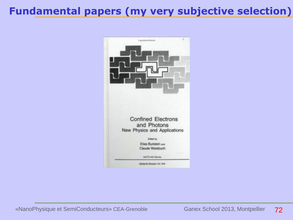
Books on the topic:
Confined Electrons and Photons: New Physics and Applications, Springer
(E. Burstein and C. Weisbuch)
Semiconductor Optics, Springer
(C. F. Klingshirn)

3«NanoPhysique et SemiConducteurs» CEA-Grenoble Ganex School 2013, Montpellier
~
1
E
hcc
14
14
10~
24.1
10.3
1
cm
eVE
Hz
m
Units

4«NanoPhysique et SemiConducteurs» CEA-Grenoble Ganex School 2013, Montpellier
Excitons and polaritons in GaN
The excitons in GaN
See Optics I (M. Leroux)
A, B and C excitons
What does an exciton look like?
A well defined wavevector for the center of mass
The electron and hole are closely bound (Bohr radius)
a (nm) EX (meV)
GaN 2.8 25
GaAs 12 4.8
The excitonic force is strong in GaN
Why is it important ?
Is it useful ?
kT @ 300K
25 meV

5«NanoPhysique et SemiConducteurs» CEA-Grenoble Ganex School 2013, Montpellier
Excitons and polaritons in GaN
Does the exciton really exist?
e
h
Kexc
e
h
Kexc
J.J. Hopfield, Phys. Rev. 112 1555 (1958)
+ Pekar, Agranovich…
Polariton = mixed exciton-photon particles

6«NanoPhysique et SemiConducteurs» CEA-Grenoble Ganex School 2013, Montpellier
JJ Hopfield
Very numerous papers on the theory of semiconductor optics…
… but his most famous paper is :

7«NanoPhysique et SemiConducteurs» CEA-Grenoble Ganex School 2013, Montpellier
0
1
2
3
4
5
En
erg
y (
eV
)
Wavevector K
Excitons and polaritons in GaN
Photon
n
ckE
Exciton
m
kEE
*
22
02
coupling
0
1
2
3
4
5
En
erg
y (
eV
)
Wavevector K

8«NanoPhysique et SemiConducteurs» CEA-Grenoble Ganex School 2013, Montpellier
3.470
3.475
3.480
3.485
3.490
En
erg
y (
eV
)
Wavevector K
Excitons and polaritons in GaN
UPB
LPB
DLT
DLT measures the intrinsic light-exciton coupling in the material
Note : in WZ GaN : A, B and C excitons + anisotropy
GaN : DLT(A)=0.8 meV GaAs : DLT=0.08 meV

9«NanoPhysique et SemiConducteurs» CEA-Grenoble Ganex School 2013, Montpellier
Consequences of the polariton pictureAbsorption
Beer-Lambert law
Propagating polariton
(attenuation = scattering)
LeII 0

10«NanoPhysique et SemiConducteurs» CEA-Grenoble Ganex School 2013, Montpellier
0
1
2
3
3.33.43.53.63.73.83.94.0
En
erg
y (
eV
)
Wavevector K
Consequences of the polariton picture
Luminescence
Polariton propagating to
the surface !
Infrared catastrophy?
Relaxation bottleneck
Thermal like population
J. J. Hopfield, J. Phys. Soc. Jap. 21 77 (1966)
Y. Toyozawa, Prog. Theor. Phys. Suppl. 12 111 (1959)

11«NanoPhysique et SemiConducteurs» CEA-Grenoble Ganex School 2013, Montpellier
Consequences of the polariton picture
Luminescence
Relaxation bottleneck
Thermal like population
around EX on UPB and LPB
3.460
3.465
3.470
3.475
3.480
3.485
3.490
3.495
3.500
En
erg
y (
eV
)
Wavevector K
Luminescence properties are very complex to model !!
(sample and experiments dependent…)
Bottleneck

12«NanoPhysique et SemiConducteurs» CEA-Grenoble Ganex School 2013, Montpellier
The polariton in GaAs

13«NanoPhysique et SemiConducteurs» CEA-Grenoble Ganex School 2013, Montpellier
Excitons and polaritons in GaN
B. Gil et al., Solid State Commun. 104 264 (1997)

14«NanoPhysique et SemiConducteurs» CEA-Grenoble Ganex School 2013, Montpellier
Confined electronic structures
The strong light-matter coupling in bulk GaN….
… creates strong polaritons, which are lousy emitters
What about QWs?
A confined exciton in a QW is coupled to a large number of photonic states
Luminescence allowed on the first order
V. M. Agranovitch and O. A. Dubovskii, JETP Lett. 3, 223 (1966)
C. Weisbuch et al., Solid State Commun. 37, 219 (1981)
The binding energy of excitons in QW is up to 4 times larger than in bulk
M. Shinada and S. Sugano, J. Phys. Soc. Jpn. 21 1936 (1966)

15«NanoPhysique et SemiConducteurs» CEA-Grenoble Ganex School 2013, Montpellier
Confined electronic structures : GaN
The QCSE reduces the exciton binding energy…
… but in thin QWs or non-polar QWs, the exciton binding energy can be large!
bulk
XE
P. Bigenwald et al., Phys. Stat. Sol. (b) 216 371 (1999)
16«NanoPhysique et SemiConducteurs» CEA-Grenoble Ganex School 2013, Montpellier
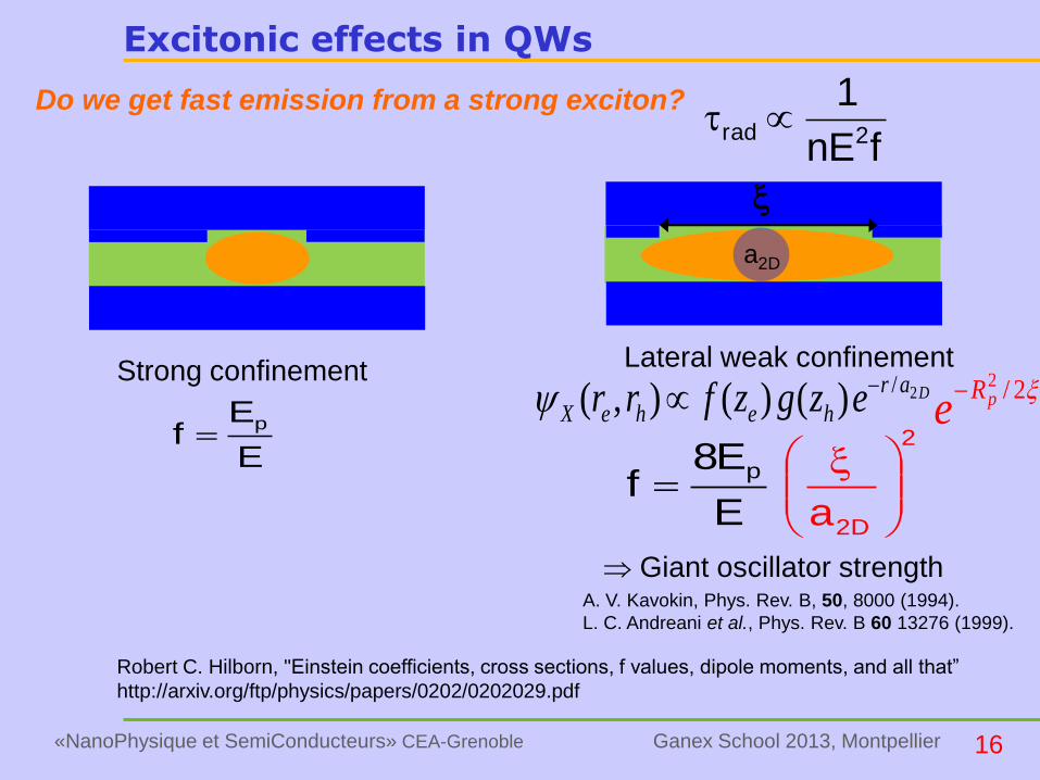
Excitonic effects in QWs
Strong confinement
E
E8f
p
2
D2a
Lateral weak confinement
a2D
E
Ef
p
22 2/ pReDar
heheX ezgzfrr 2/)()(),(
A. V. Kavokin, Phys. Rev. B, 50, 8000 (1994).
L. C. Andreani et al., Phys. Rev. B 60 13276 (1999).
Giant oscillator strength
fnE
12rad
Robert C. Hilborn, "Einstein coefficients, cross sections, f values, dipole moments, and all that”
http://arxiv.org/ftp/physics/papers/0202/0202029.pdf
Do we get fast emission from a strong exciton?

17«NanoPhysique et SemiConducteurs» CEA-Grenoble Ganex School 2013, Montpellier
Excitonic effects in QWs
2D limit = intrinsic lifetime of two-dimensional exciton
~ 10 ps for a GaAs/AlAs QW
L. C. Andreani et al., Solid State Commun. 77 641 (1991)
B. Deveaud et al., Phys. Rev. Lett. 67 2355 (1991)
Dephasing (exciton-exciton or exciton-phonon scattering) limits the
coherence surface and hence the radiative emission rate

18«NanoPhysique et SemiConducteurs» CEA-Grenoble Ganex School 2013, Montpellier
Excitonic effects in QWs
The 2D quantum well excitons does couple efficiently to photons!
In a non perfect structure, the fundamental emitting state will be
laterally localized states
Even in a very good (i.e. III-As) quantum well, it takes very peculiar
experimental conditions to observe the intrinsic fast lifetimes of 2D excitons
- Very low temperature (phonon scattering)
- Resonant and low excitation (carrier-carrier scattering)
19«NanoPhysique et SemiConducteurs» CEA-Grenoble Ganex School 2013, Montpellier
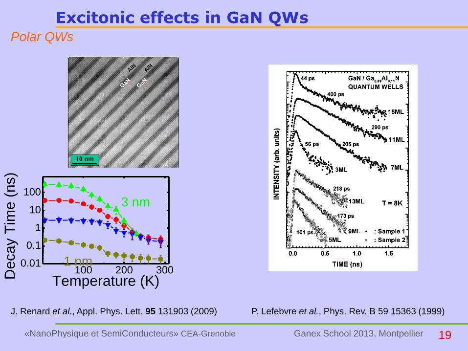
Excitonic effects in GaN QWs
100 200 3000.01
0.1
1
10
100
Decay T
ime (
ns)
Temperature (K)
Polar QWs
3 nm
1 nm
J. Renard et al., Appl. Phys. Lett. 95 131903 (2009) P. Lefebvre et al., Phys. Rev. B 59 15363 (1999)

20«NanoPhysique et SemiConducteurs» CEA-Grenoble Ganex School 2013, Montpellier
Excitonic effects in GaN QWs
Non-Polar QWs
P. Waltereit et al., Nature, 406 865 (2000)
P. Corfdir et al., Phys. Rev. B 83 245326 (2011)

21«NanoPhysique et SemiConducteurs» CEA-Grenoble Ganex School 2013, Montpellier
Excitonic effects in GaN QWsIs 100 ps @ 3.5 eV a fast recombination??
fnE
12rad
GaAs QW emitting at 1.7 eV with a lifetime of 25 ps : f=320
GaN QW emitting at 3.5 eV with a lifetime of 100 ps : f=24
Strong excitonic effects in III-N, but ordinary recombination rates
Quite strong localization effects, no giant oscillator strength

22«NanoPhysique et SemiConducteurs» CEA-Grenoble Ganex School 2013, Montpellier
Microcavity physics
More control on light-matter coupling
What are microcavities ?
How does an emitter in a microcavity behave ?
Strong coupling
Weak coupling
Two-dimensional microcavity polaritons
Peculiarities of the III-N system

23«NanoPhysique et SemiConducteurs» CEA-Grenoble Ganex School 2013, Montpellier
Optical cavities
What is a mode of the E-M field?
A solution of Maxwell equations in the absence of source
What is a confined mode?
« An optical resonator, the optical counterpart of an electronic resonant circuit,
confines and stores light at certain resonant frequencies »
« Fundamentals of photonics »
B.E.A. Saleh and M.C. Teich, Wiley ed.
« Optical resonators [...] are used primarily in order to build up large field
intensities with moderate power inputs. They consist in most cases of two,
or more, curved mirrors that serve to "trap," by repeated reflections and
refocusing, an optical beam that thus becomes the mode of the resonator. »
« Optical electronics in modern communications »
A. Yariv, Oxford ed.

24«NanoPhysique et SemiConducteurs» CEA-Grenoble Ganex School 2013, Montpellier
Optical cavities
High intensity in a confined region of space for resonant frequencies
Quality factor measures the decay of stored E-M energy in mode :
Q
t
0eEE

25«NanoPhysique et SemiConducteurs» CEA-Grenoble Ganex School 2013, Montpellier
Various semiconductor microcavities
1 µm
2 µm

26«NanoPhysique et SemiConducteurs» CEA-Grenoble Ganex School 2013, Montpellier
Spontaneous emission : irreversible emission of a photon
2
2sp iHf2
Spontaneous emission
Mirror
Influence of the E-M surrounding:

27«NanoPhysique et SemiConducteurs» CEA-Grenoble Ganex School 2013, Montpellier
2
2sp iHf2
Spontaneous emission
Control of the emitter-field
coupling
Control of the density of states
for the EM field
Cavity Quantum ElectroDynamics

28«NanoPhysique et SemiConducteurs» CEA-Grenoble Ganex School 2013, Montpellier
Free space
0 200 400 600 800 10000.0
0.2
0.4
0.6
0.8
1.0
P(e
xcite
d s
tate
)
Time
Free space emission
3
0
232
2spc3
d2iHf
2
0

29«NanoPhysique et SemiConducteurs» CEA-Grenoble Ganex School 2013, Montpellier
Isolated system : strong coupling
0 200 400 600 800 1000
0.0
0.2
0.4
0.6
0.8
1.0
P(e
xcite
d st
ate)
Time
2ħW
Energy
|g, 1> |e, 0>
Photon/emitter
hybrid eigenstates
Strong coupling
W Rabi frequency
V2
d
0
2
W
/W
Perfect mirrors
d transition dipole, V mode volume

30«NanoPhysique et SemiConducteurs» CEA-Grenoble Ganex School 2013, Montpellier
Damped strong coupling
0 200 400 600 800 1000
0.0
0.2
0.4
0.6
0.8
1.0
P(e
xcite
d st
ate)
Time
Strong coupling
W Rabi frequency
cav cavity damping (Q=cav/cav)
at atomic decay in other modes
W>(cav, at)
/W
atcav.te
cav
at
In general cav>>at

31«NanoPhysique et SemiConducteurs» CEA-Grenoble Ganex School 2013, Montpellier
0 200 400 600 800 1000
0.0
0.2
0.4
0.6
0.8
1.0
P(e
xcite
d st
ate
)
Time
Weak coupling, Purcell effect
W<cav
2 unperturbed eigenstates
modified decay rates
0
= Fp 0
Fp Purcell factor

32«NanoPhysique et SemiConducteurs» CEA-Grenoble Ganex School 2013, Montpellier
Weak coupling, Purcell effect
E.M. Purcell
Phys. Rev. 69, 681 (1946)
A famous paper :

33«NanoPhysique et SemiConducteurs» CEA-Grenoble Ganex School 2013, Montpellier
Weak coupling, emission diagram modification
Example : 1 atom in a Fabry-Pérot cavity, emitting at
A. Kastler, Appl. Optics 1,17 (1962)
L
q
ncav
reflection
coefficient r
2i22
1
2
er1
2cosr*2r1,I
q
d
c
cosdn
ccosLn
cav1
cav
q
q

34«NanoPhysique et SemiConducteurs» CEA-Grenoble Ganex School 2013, Montpellier
Weak coupling, emission diagram modification
A. Kastler, Appl. Optics 1,17 (1962)
Emission for a centered atom (varying ) at normal incidence, r=0.9
0 1 2 3 4 5 6
I(
, q=
0)
in(2c)/(ncav
L))
Free spectral
range

35«NanoPhysique et SemiConducteurs» CEA-Grenoble Ganex School 2013, Montpellier
Weak coupling, emission diagram modification
A. Kastler, Appl. Optics 1,17 (1962)
0
30
60
90
120
150
180
210
240
270
300
330
Monochromatic atom at =5(2c)/(ncavL)
directional emission
Only spectral and angular intensity redistribution
No spontaneous emission rate modification!!
But can be used to extract more light out of a high index material !!
H. Benisty, H. De Neve and C.Weisbuch, IEEE J. Quantum Electron., 34, pp. 1612–1643 (1998)

36«NanoPhysique et SemiConducteurs» CEA-Grenoble Ganex School 2013, Montpellier
Weak coupling, emission diagram modification
A. Kastler, Appl. Optics 1,17 (1962)
0
30
60
90
120
150
180
210
240
270
300
330
Only spectral and angular intensity redistribution
No spontaneous emission rate modification!!
37«NanoPhysique et SemiConducteurs» CEA-Grenoble Ganex School 2013, Montpellier
Weak coupling, emission diagram modification
A. Kastler, Appl. Optics 1,17 (1962)

38«NanoPhysique et SemiConducteurs» CEA-Grenoble Ganex School 2013, Montpellier
Key ideas
Spontaneous emission depends on the E-M field mode structure
The SE radiation pattern is in general modified by the E-M field boundaries
When resonantly coupled to a cavity mode, the SE rate can be modified:
- Weak coupling : faster SE in the « overdamped » regime
=> Purcell effect
- Strong coupling : damped reversible SE
=> mixed emitter-photon modes

39«NanoPhysique et SemiConducteurs» CEA-Grenoble Ganex School 2013, Montpellier
Strong coupling in a planar cavity
Quantum Well
In-plane translational invariance for confined field and QW excitons
one to one coupling of confined modes and excitons of same kx,y
GaN
AlGaN
yxyxDRKiar
heheX eezgzfrr ,,2./)()(),(
he
h
y,x
e
y,xy,x*
h
*
e
h
*
he
*
e
y,xrrr,kkK,
mm
rmrmR
1 nm
AlGaN

40«NanoPhysique et SemiConducteurs» CEA-Grenoble Ganex School 2013, Montpellier
Strong coupling in a planar cavity
anticrossing at resonance
Creation of mixed exciton-photon states : 2D polaritons
C. Weisbuch et al., Phys. Rev. Lett. 69, 3314 (1992)

41«NanoPhysique et SemiConducteurs» CEA-Grenoble Ganex School 2013, Montpellier
Bragg mirrors
DBR = Distributed Bragg Reflector
rely on periodicity to have Bragg reflection
Lh=0/(4nh) Ll=0/(4nl)
nh nl
Reflection at each interface
At resonant wavelength:
- Constructive reflection interference
- Destructive propagation interference

42«NanoPhysique et SemiConducteurs» CEA-Grenoble Ganex School 2013, Montpellier
Bragg mirrors
0.7 0.8 0.9 1.0 1.1 1.2 1.30.0
0.2
0.4
0.6
0.8
1.0
R
Energy (eV)
0.7 0.8 0.9 1.0 1.1 1.2 1.30.0
0.2
0.4
0.6
0.8
1.0
R
Energy (eV)
0.7 0.8 0.9 1.0 1.1 1.2 1.30.0
0.2
0.4
0.6
0.8
1.0
R
Energy (eV)nsub=3.5
DBR N pairs
nh=3.5 (GaAs), nl=2.95 (AlAs)
resonant at E=1eV (=1.24µm)
nsup=1
N2
h
l
sub
sup
maxn
n
n
n41R
lh
lhres
nn
nnE4E
D
DE
N=9
N=15
N=21, Rmax=0.9991
Varying E

43«NanoPhysique et SemiConducteurs» CEA-Grenoble Ganex School 2013, Montpellier
Comparison of III-N and III-As systems
III-As III-N
nGaAs=3.5, nAlAs=3
Lattice-matched
R=99%
N=16
nGaN=2.3, nAlN=2.1
Lattice mismatch=2.4%
R=99%
N=20 to 60 for GaN/AlGaN DBR
Al0.2Ga0.8N/Al0.85In0.15N
Lattice matched
R=99%
N=27
E. Feltin et al., Appl. Phys. Lett. 88 051108 (2006)
N2
h
l
sub
sup
maxn
n
n
n41R

44«NanoPhysique et SemiConducteurs» CEA-Grenoble Ganex School 2013, Montpellier
DBR based Fabry-Pérot
nsub=2.3
-cavity, nh
Varying E
0.7 0.8 0.9 1.0 1.1 1.2 1.30.0
0.2
0.4
0.6
0.8
1.0
R
Energy (eV)
0.9990 0.9995 1.0000 1.0005 1.00100.0
0.2
0.4
0.6
0.8
1.0
R
Energy (eV)
DE=E/Q
Q typically
103 => 104
(cav : 0.5 => 5 ps)
Transmission=1
on resonance for
perfectly balanced
mirrors

45«NanoPhysique et SemiConducteurs» CEA-Grenoble Ganex School 2013, Montpellier
Bragg mirrors as 1D photonic band gap
R. P. Stanley et al., Phys. Rev. A 48, 2246 (1993)
Analogy between Maxwell and Schrödinger equations
the Bragg reflector as a 1D photonic bandgap
varying the height of one layer introduces
an impurity state in the gap

46«NanoPhysique et SemiConducteurs» CEA-Grenoble Ganex School 2013, Montpellier
DBR based Fabry-Pérot
-1.5 -1.0 -0.5 0.0 0.5 1.0 1.5
0
50
100
150
200
250
300
Refr
active index
Fie
ld inte
nsity
z (µm)
2.6
2.8
3.0
3.2
3.4
3.6
3.8
4.0
Longitudinal E-M field profile at resonance:
Field peaked at cavity center, exponential decay in the DBRs
Mode extent larger than for metal mirror cavity!

47«NanoPhysique et SemiConducteurs» CEA-Grenoble Ganex School 2013, Montpellier
Planar microcavities : the photon effective mass
L
q
ncav
reflection
coefficient r
Resonance condition : L
pkz
cL
pnm
m
k
Ln
cpk
L
p
n
cE
cavph
ph
yx
cav
yx
cav
*
*
2
,
2
2
,
2
2

48«NanoPhysique et SemiConducteurs» CEA-Grenoble Ganex School 2013, Montpellier
-2x10⁵
-1x10⁵ 0 1x10
52x10
5
1.498
1.500
1.502
1.504
1.506
1.508
En
erg
y (
eV
)
kx,y
(cm-1)
Strong coupling in a planar cavity
-2x10⁵
-1x10⁵ 0 1x10
52x10
5
1.498
1.500
1.502
1.504
1.506
1.508
En
erg
y (
eV
)
kx,y
(cm-1)
selection
rule
Ephoton
Eexciton
mph~10-5 me
mexc~10-1 me
New dispersion relation :
Lower polariton
Upper polariton
« Exciton-like »
(confined photon + exciton)
Fast (~5 ps) desintegration through photon escape
100% directional extraction through top mirror
*
2
//
2
0,
//,
2
//
2
0,
2
2
Ph
PhPh
X
XX
m
kEE
M
KEE

49«NanoPhysique et SemiConducteurs» CEA-Grenoble Ganex School 2013, Montpellier
-2x10⁵
-1x10⁵ 0 1x10
52x10
5
1.498
1.500
1.502
1.504
1.506
1.508
En
erg
y (
eV
)
kx,y
(cm-1)
Strong coupling in a planar cavity
-2x10⁵
-1x10⁵ 0 1x10
52x10
5
1.498
1.500
1.502
1.504
1.506
1.508
En
erg
y (
eV
)
kx,y
(cm-1)
selection
rule
Ephoton
Eexciton
mph~10-5 me
mexc~10-1 me
Relaxation bottleneck
(high DOS vs low DOS at kx,y~0)
BUT excitons = bosons in the low density regime
Stimulated emission of polaritons : R=R0(1+<N>)
Polariton laser or solid-state BEC
F. Tassone et al., Phys. Rev. B 53, R7642 (1996)
A. Imamoglu et al.
Phys. Rev. A 53, 4250 (1996)
Condition for
condensation
2
2
h
m
Tk
n
B

50«NanoPhysique et SemiConducteurs» CEA-Grenoble Ganex School 2013, Montpellier
Strong coupling in a planar cavity
J. Kasprzak et al., Nature 443, 409 (2006)
"Bose–Einstein condensation of exciton polaritons"
reach stimulated relaxation of polaritons before exciton screening
51«NanoPhysique et SemiConducteurs» CEA-Grenoble Ganex School 2013, Montpellier
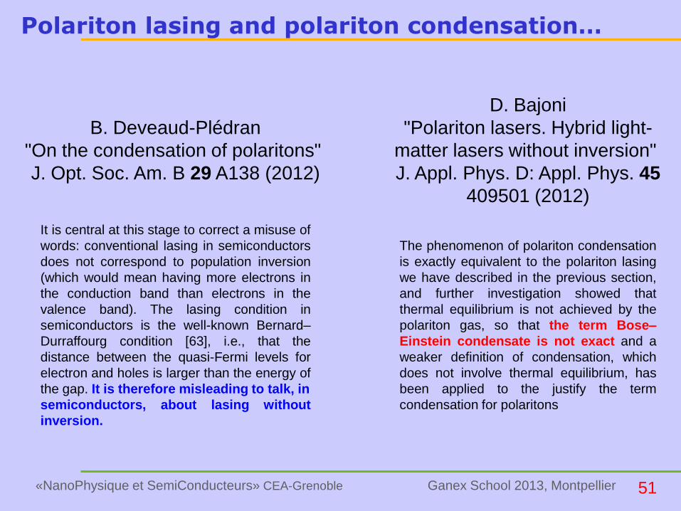
Polariton lasing and polariton condensation…
B. Deveaud-Plédran
"On the condensation of polaritons"
J. Opt. Soc. Am. B 29 A138 (2012)
D. Bajoni
"Polariton lasers. Hybrid light-
matter lasers without inversion"
J. Appl. Phys. D: Appl. Phys. 45
409501 (2012)
The phenomenon of polariton condensation
is exactly equivalent to the polariton lasing
we have described in the previous section,
and further investigation showed that
thermal equilibrium is not achieved by the
polariton gas, so that the term Bose–
Einstein condensate is not exact and a
weaker definition of condensation, which
does not involve thermal equilibrium, has
been applied to the justify the term
condensation for polaritons
It is central at this stage to correct a misuse of
words: conventional lasing in semiconductors
does not correspond to population inversion
(which would mean having more electrons in
the conduction band than electrons in the
valence band). The lasing condition in
semiconductors is the well-known Bernard–
Durraffourg condition [63], i.e., that the
distance between the quasi-Fermi levels for
electron and holes is larger than the energy of
the gap. It is therefore misleading to talk, in
semiconductors, about lasing without
inversion.

52«NanoPhysique et SemiConducteurs» CEA-Grenoble Ganex School 2013, Montpellier
Strong coupling with nitrides
Reference system : GaAs/AlAs cavities, InGaAs QWs
Very large Q factors (10000-50000)
long polariton lifetime ~15 ps and little disorder induced localization
But : restricted to low temperatures
restricted to low pump powers
III-N system:
Large intrinsic light matter coupling
QW exciton stable at 300 K, more stable at large pump power
But : high quality mirrors difficult to fabricate, much photonic disorder

53«NanoPhysique et SemiConducteurs» CEA-Grenoble Ganex School 2013, Montpellier
Strong coupling with nitrides
The "Mott density" for 2D excitons
225
1
Ban
a (nm) Nmott(cm-2)
GaN 2.8 5 1011
GaAs 12 2.5 1010
Smooth transition to e-h plasma, due to phase-space filling
N. F. Mott, Philos. Mag. 6 287 (1961)
S. Schmitt-Rink et al., Phys. Rev. B 32 6601 (1985)

54«NanoPhysique et SemiConducteurs» CEA-Grenoble Ganex School 2013, Montpellier
Strong coupling with nitrides

55«NanoPhysique et SemiConducteurs» CEA-Grenoble Ganex School 2013, Montpellier
Strong coupling with nitrides
First demonstration:
Bulk GaN, Q~100, 5 K, but strong coupling W=30 meV
A. Antoine-Vincent et al., Phys. Rev. B 68 153313 (2003)

56«NanoPhysique et SemiConducteurs» CEA-Grenoble Ganex School 2013, Montpellier
Strong coupling with nitridesF. Semond et al., Appl. Phys. Lett. 87 021102 (2005)
Room temperature strong coupling !
R. Butté et al., Phys. Rev. B 73 033315 (2006)

57«NanoPhysique et SemiConducteurs» CEA-Grenoble Ganex School 2013, Montpellier
Strong coupling with nitrides
W=50 meV
G. Christmann et al., Phys. Rev. B 77 085310 (2008)
NW
For N QWs

58«NanoPhysique et SemiConducteurs» CEA-Grenoble Ganex School 2013, Montpellier
Strong coupling with nitrides
Room temperature polariton lasing
G. Christmann et al., Appl. Phys. Lett. 93 051102 (2008)

59«NanoPhysique et SemiConducteurs» CEA-Grenoble Ganex School 2013, Montpellier
The Purcell effect
Practical situation
=cav+leak~0(Fp+1)
b=(photons in confined mode)/(emitted photons)=cav/
leak
cav=Fp0
b=Fp/(Fp+1)
For high Fp, monomode emission without inhibition!!
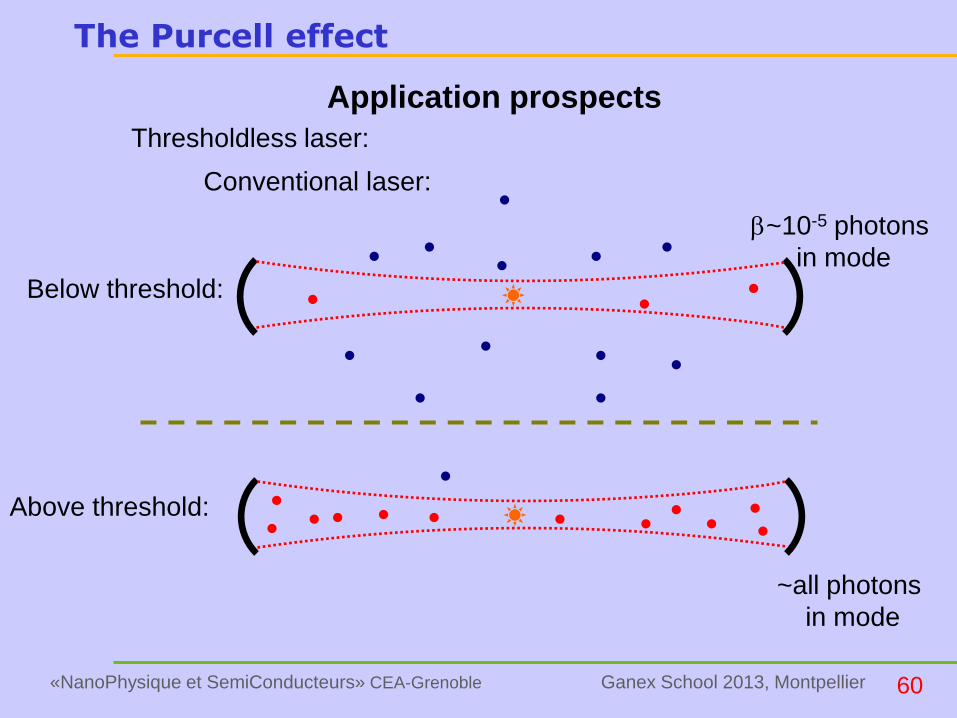
60«NanoPhysique et SemiConducteurs» CEA-Grenoble Ganex School 2013, Montpellier
The Purcell effect
Application prospects
Thresholdless laser:
Conventional laser:
Below threshold:
Above threshold:
b~10-5 photons
in mode
~all photons
in mode

61«NanoPhysique et SemiConducteurs» CEA-Grenoble Ganex School 2013, Montpellier
The Purcell effect
Thresholdless laser:
High b regime : all photons feed into mode below threshold!!
ln(b)
Pth= cav (1+b)/2b => Pth scales as 1/b
For b~1 and Q~10000, Pth ~ 20 nA!Y. Yamamoto et al., Phys. Rev. A 44, 657 (1991)
T. Kobayashi et al., Tech. Dig. of 43rd Fall meeting of
Japanese Applied Physics Society, paper 29a-B-6 (1982)
n1
n1nP cav
inb
b
laser

62«NanoPhysique et SemiConducteurs» CEA-Grenoble Ganex School 2013, Montpellier
Whispering gallery modes confined by total internal reflection
G. Mie, Ann. Phys. (NY) 25, 377 (1908)
Lord Rayleigh, « The problem of the whispering gallery », Scientic Papers 5, 617 (1912)
E2
Various nitride microcavities

63«NanoPhysique et SemiConducteurs» CEA-Grenoble Ganex School 2013, Montpellier
Various nitride microcavities
Lasing at room temperature in a microlaser
Q~4000
A. C. Tamboli et al., Nature Photon. 1 61 (2007)
InGaN QWs in a GaN slab
64«NanoPhysique et SemiConducteurs» CEA-Grenoble Ganex School 2013, Montpellier
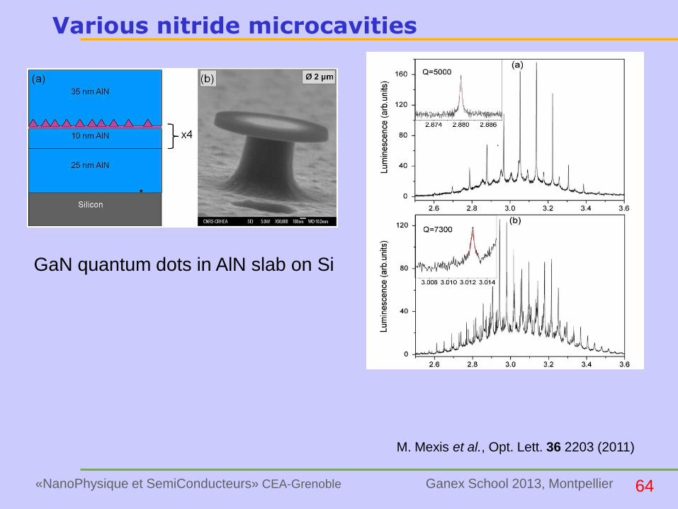
Various nitride microcavities
GaN quantum dots in AlN slab on Si
M. Mexis et al., Opt. Lett. 36 2203 (2011)

65«NanoPhysique et SemiConducteurs» CEA-Grenoble Ganex School 2013, Montpellier
Various nitride microcavities
M. Arita et al., Appl. Phys. Exp. 5 126502 (2012)

66«NanoPhysique et SemiConducteurs» CEA-Grenoble Ganex School 2013, Montpellier
Various nitride microcavities
D. Sam-Giao et al., Appl. Phys. Lett. 100 191104 (2012)
GaN quantum dots in AlN on Si

67«NanoPhysique et SemiConducteurs» CEA-Grenoble Ganex School 2013, Montpellier
Various nitride microcavities
Prospects
- UV microlasers based on the Purcell effect
- Strong coupling in other geometries than planar cavity
Strong coupling in photonic crystal slabs
68«NanoPhysique et SemiConducteurs» CEA-Grenoble Ganex School 2013, Montpellier
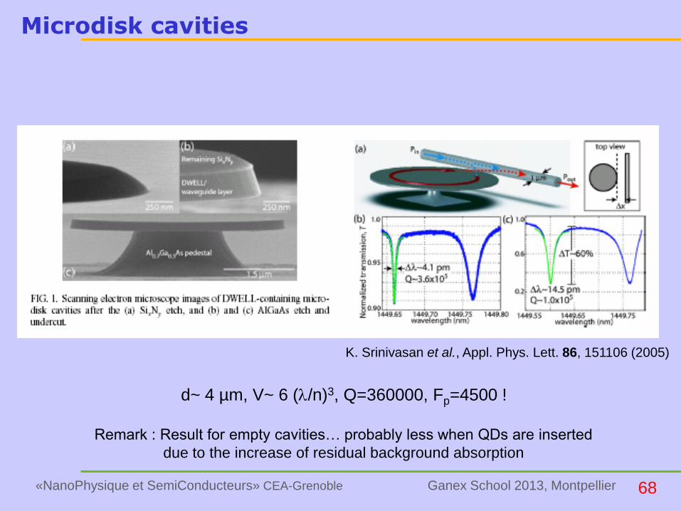
Microdisk cavities
d~ 4 µm, V~ 6 (/n)3, Q=360000, Fp=4500 !
Remark : Result for empty cavities… probably less when QDs are inserted
due to the increase of residual background absorption
K. Srinivasan et al., Appl. Phys. Lett. 86, 151106 (2005)

69«NanoPhysique et SemiConducteurs» CEA-Grenoble Ganex School 2013, Montpellier
2D photonic band gap cavities
Y. Akahane et al., Nature 425, 944 (2003)
Q=35000
Fp~4000
100 nm

70«NanoPhysique et SemiConducteurs» CEA-Grenoble Ganex School 2013, Montpellier
Fundamental papers (my very subjective selection)

71«NanoPhysique et SemiConducteurs» CEA-Grenoble Ganex School 2013, Montpellier
Fundamental papers (my very subjective selection)
72«NanoPhysique et SemiConducteurs» CEA-Grenoble Ganex School 2013, Montpellier
Fundamental papers (my very subjective selection)