BROADBAND HIGH EFFICIENCY CLASS J POWER ...eece.cu.edu.eg/~hfahmy/thesis/2013_07_amp.pdfBROADBAND...
94
BROADBAND HIGH EFFICIENCY CLASS J POWER AMPLIFIER FOR A COGNITIVE RADIO SYSTEM By Ahmed Eissa Fathy Khorshid A Thesis Submitted to the Faculty of Engineering at Cairo University In Partial Fulfillment of the Requirements for the Degree of MASTER OF SCIENCE In Electronics and Electrical Communications Engineering FACULTY OF ENGINEERING, CAIRO UNIVERSITY GIZA, EGYPT 2013
-
Upload
hoangtuyen -
Category
Documents
-
view
219 -
download
1
Transcript of BROADBAND HIGH EFFICIENCY CLASS J POWER ...eece.cu.edu.eg/~hfahmy/thesis/2013_07_amp.pdfBROADBAND...
BROADBAND HIGH EFFICIENCY CLASS J POWER
AMPLIFIER FOR A COGNITIVE RADIO SYSTEM
By
Ahmed Eissa Fathy Khorshid
A Thesis Submitted to the Faculty of Engineering at Cairo University
In Partial Fulfillment of the Requirements for the Degree of
MASTER OF SCIENCE In
Electronics and Electrical Communications Engineering
FACULTY OF ENGINEERING, CAIRO UNIVERSITY GIZA, EGYPT
2013


Engineer’s Name: Ahmed Eissa Fathy Khorshid Date of Birth: 3/6/1988 Nationality: Egyptian E-mail: [email protected] Phone: 01224601246 Address: 3 Rashdan street, Dokki, Giza. Registration Date: 1/10/2010 Awarding Date: / / Degree: Master of Science Department: Electronics and Electrical Communications Engineering
Supervisors: Prof. Hossam Ali Hassan Fahmy
Prof. Islam Abdel Sattar Ahmed Eshrah Prof. Ali Mohamed Ali Darwish
Examiners: Prof. Ahmed Abdel Nazir Ahmed Mohamed (External
examiner) (MTC) Prof. Magdi Fikri Mohamed Regaie (Internal examiner) Prof. Hossam Ali Hassan Fahmy (Thesis main advisor)
Prof. Islam Abdel Sattar Ahmed Eshrah (Member) Prof. Ali Mohamed Ali Darwish (Member)
Title of Thesis:
Broadband High Efficiency Class J Power Amplifier for a Cognitive Radio System Key Words: Power Amplifiers; Broadband; Efficiency; Class J; Load-pull.
Summary:
In communication systems, low operational cost and high data-handling capability are considered as cornerstones in the targeted specifications. Since a large portion of total power consumption in the system occurs at the Power Amplifier (PA) stage, the strictness of the PA design specifications becomes unquestionable in order to minimize the power losses and thus improve the system performance. In this work, after conducting an in-depth research in the available PA classes as well as new techniques suggested in the recent few years, a broadband, high efficiency Class-J PA is proposed as a part of the RF front-end of a Cognitive Radio system operating in the TV band, for the first time that such class is used in this band. The proposed PA design covers the frequency band from 0.4 GHz till 1 GHz, reaching a percentage bandwidth of 85.7%, which is the highest to be achieved with a Class J PA in the literature so far, and with efficiency above 60% over that whole bandwidth of operation.
Insert photo here

i
Acknowledgments
First and foremost, I am thankful to “Allah” the most generous and the most merciful, for without his grace, this thesis would never have been accomplished.
I am grateful to my father, mother and brother for their continuous support, help and advice.
I am deeply indebted to my grandfather and my grandmother, who have always advised me never to withdraw from the academic path, and to keep learning and developing new ideas throughout my life.
Special thanks to my supervisors: Dr. Ali Darwish, Dr. Islam Eshrah and Dr. Hossam Fahmy, for they have been my mentors and advisors throughout this work, guiding me all the way through this important stage in my life, helping me in overcoming all the obstacles, and developing in me the spirit of productive and moral research .
I would also like to express my gratitude to all my professors and colleagues at the Electronics and Communication Department, Faculty of Engineering, Cairo University, for their support and sincere advices.
I also would like to thank the engineers at the Electronics Department at the National Telecommunication Institute (NTI), for their great help in the circuit fabrication.
I would like also to thank the National Telecom Regulatory Authority (NTRA) for supporting this project.
Finally, special thanks to the engineers and technicians at the Electronics Department at the American University in Cairo (AUC) for their aid and support in setting up the measurement equipment.

ii
Table of Contents
ACKNOWLEDGMENTS ............................................................................................. I
TABLE OF CONTENTS .............................................................................................. II
LIST OF TABLES .......................................................................................................IV
LIST OF FIGURES ...................................................................................................... V
LIST OF ACRONYMS ............................................................................................ VIII
LIST OF SYMBOLS ....................................................................................................IX
ABSTRACT ................................................................................................................... X
CHAPTER 1 : INTRODUCTION ................................................................................ 1
CHAPTER 2 : REVIEW ON COGNITIVE RADIO .................................................. 3
2.1. HISTORY .............................................................................................. 3 2.2. DEFINITION .......................................................................................... 3 2.3. COGNITIVE RADIO SYSTEM CAPABILITIES ........................................... 5 2.4. TV BAND COGNITIVE RADIO SYSTEM ................................................. 6
CHAPTER 3 : OVERVIEW ON POWER AMPLIFIER TECHNOLOGY ............ 7
3.1. HISTORICAL BACKGROUND ................................................................. 7 3.2. BASIC POWER AMPLIFIER PARAMETERS .............................................. 7 3.3. CLASSICAL POWER AMPLIFIERS ........................................................... 8
3.3.1. Class A, B, AB and C Power Amplifiers ................................................ 9 3.3.1.1. Class A Power Amplifiers ........................................................................................ 10 3.3.1.2. Class B Power Amplifiers ........................................................................................ 11 3.3.1.3. Class AB Power Amplifiers ..................................................................................... 13 3.3.1.4. Class C Power Amplifiers ........................................................................................ 13
3.3.2. Switching Power Amplifiers ................................................................. 14 3.3.2.1. Class D Power Amplifiers ........................................................................................ 14 3.3.2.2. Class E Power Amplifiers ........................................................................................ 16
3.3.3. Class F Power Amplifiers ..................................................................... 18 3.3.4. Summary for the classical Power Amplifiers ........................................ 20
3.4. CLASS J POWER AMPLIFIERS .............................................................. 21 3.4.1. Class J Power Amplifier features .......................................................... 22 3.4.2. Class J State of the Art Implementations .............................................. 23 3.4.3. Load Pull Contours ............................................................................... 24
3.5. TV BAND POWER AMPLIFIER ............................................................ 25
CHAPTER 4 : PROPOSED CLASS J POWER AMPLIFIER DESIGN ............... 26
4.1. DESIGN METHODOLOGY .................................................................... 26 4.1.1. The Active Element .............................................................................. 26 4.1.2. The Biasing Circuit ............................................................................... 26 4.1.3. Output Matching Circuit ....................................................................... 26 4.1.4. Input Matching Circuit .......................................................................... 27

iii
4.2. POWER AMPLIFIER DESIGN IMPLEMENTATION................................... 28 4.2.1. Selection of The Active Element .......................................................... 28 4.2.2. Class J Biasing ...................................................................................... 29 4.2.3. Output matching Circuit ........................................................................ 31 4.2.4. Input Matching Circuit .......................................................................... 36 4.2.5. Circuit Layout and Optimization .......................................................... 40 4.2.6. Circuit fabrication ................................................................................. 45
CHAPTER 5 : RESULTS ............................................................................................ 46
5.1. SIMULATION RESULTS ....................................................................... 46 5.1.1. Circuit Simulation Using Circuit Simulator .......................................... 46 5.1.2. Post Layout Simulation ......................................................................... 49
5.1.2.1. Linearity ................................................................................................................... 55 5.2. EXPERIMENTAL RESULTS ................................................................... 58
CHAPTER 6 : CONCLUSION AND FUTURE WORK .......................................... 67
APPENDIX A: CREE CGH40010 GAN HEMT ....................................................... 68
APPENDIX B: STABILITY TESTS .......................................................................... 72
REFERENCES ............................................................................................................. 73

iv
List of Tables
Table 1: Summary for the classical modes of operation for PAs ................................... 21 Table 2: Summary for recent implementations for Class J ............................................ 23 Table 3: Biasing voltages selected for Class J operation ............................................... 29 Table 4: Final values for the circuit elements used ........................................................ 41 Table 5: Comparison between this work and previous implementations for Class J PAs ........................................................................................................................................ 66
v
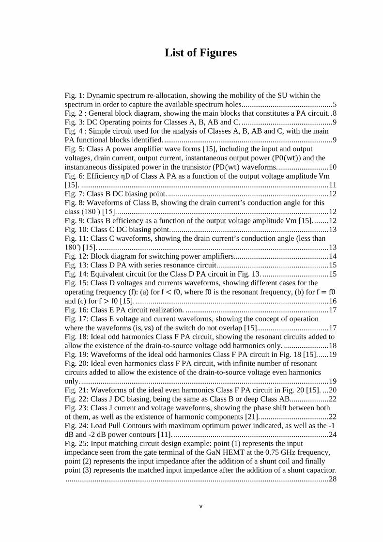
List of Figures
Fig. 1: Dynamic spectrum re-allocation, showing the mobility of the SU within the spectrum in order to capture the available spectrum holes............................................... 5 Fig. 2 : General block diagram, showing the main blocks that constitutes a PA circuit. . 8 Fig. 3: DC Operating points for Classes A, B, AB and C. ............................................... 9 Fig. 4 : Simple circuit used for the analysis of Classes A, B, AB and C, with the main PA functional blocks identified. ....................................................................................... 9 Fig. 5: Class A power amplifier wave forms [15], including the input and output voltages, drain current, output current, instantaneous output power (P0(wt)) and the instantaneous dissipated power in the transistor (PD(wt) waveforms. .......................... 10 Fig. 6: Efficiency ηD of Class A PA as a function of the output voltage amplitude Vm [15]. ................................................................................................................................ 11 Fig. 7: Class B DC biasing point. ................................................................................... 12 Fig. 8: Waveforms of Class B, showing the drain current’s conduction angle for this class (180 ̊) [15]. ............................................................................................................. 12 Fig. 9: Class B efficiency as a function of the output voltage amplitude Vm [15]. ....... 12 Fig. 10: Class C DC biasing point. ................................................................................. 13 Fig. 11: Class C waveforms, showing the drain current’s conduction angle (less than 180 ̊) [15]. ....................................................................................................................... 13 Fig. 12: Block diagram for switching power amplifiers. ................................................ 14 Fig. 13: Class D PA with series resonance circuit.......................................................... 15 Fig. 14: Equivalent circuit for the Class D PA circuit in Fig. 13. .................................. 15 Fig. 15: Class D voltages and currents waveforms, showing different cases for the operating frequency (f): (a) for f < f0, where f0 is the resonant frequency, (b) for f = f0 and (c) for f > f0 [15]. .................................................................................................... 16 Fig. 16: Class E PA circuit realization. .......................................................................... 17 Fig. 17: Class E voltage and current waveforms, showing the concept of operation where the waveforms (is, vs) of the switch do not overlap [15]..................................... 17 Fig. 18: Ideal odd harmonics Class F PA circuit, showing the resonant circuits added to allow the existence of the drain-to-source voltage odd harmonics only. ....................... 18 Fig. 19: Waveforms of the ideal odd harmonics Class F PA circuit in Fig. 18 [15]. ..... 19 Fig. 20: Ideal even harmonics class F PA circuit, with infinite number of resonant circuits added to allow the existence of the drain-to-source voltage even harmonics only. ................................................................................................................................ 19 Fig. 21: Waveforms of the ideal even harmonics Class F PA circuit in Fig. 20 [15]. ... 20 Fig. 22: Class J DC biasing, being the same as Class B or deep Class AB.................... 22 Fig. 23: Class J current and voltage waveforms, showing the phase shift between both of them, as well as the existence of harmonic components [21]. ................................... 22 Fig. 24: Load Pull Contours with maximum optimum power indicated, as well as the -1 dB and -2 dB power contours [11]. ................................................................................ 24 Fig. 25: Input matching circuit design example: point (1) represents the input impedance seen from the gate terminal of the GaN HEMT at the 0.75 GHz frequency, point (2) represents the input impedance after the addition of a shunt coil and finally point (3) represents the matched input impedance after the addition of a shunt capacitor. ........................................................................................................................................ 28

vi
Fig. 26: The circuit used in MWO to determine the IV characteristics for the GaN HEMT. ............................................................................................................................ 29 Fig. 27: Drain current ID plotted versus the gate-to-source voltage VGS (at different values for the drain-to-source voltage VDS ) for the CGH40010 GaN HEMT model. . 30 Fig. 28 : Drain current ID plotted versus the drain-to-source voltage VDS (at different values for the gate-to-source voltages VGS) for the CGH40010 GaN HEMT model. ... 30 Fig. 29: Load-Pull setup used on the MWO simulator to draw the constant gain and PAE contours. ................................................................................................................. 31 Fig. 30: PAE constant contours at 500 MHz, with the arrow indicating the direction of PAE increase. ................................................................................................................. 32 Fig. 31: Required loads for achieving maximum PAE over the frequency band from 0.5 GHz till 1 GHz, calculated using the load-pull wizard. ................................................. 32 Fig. 32: Constant gain contours at the 500 MHz frequency, with the arrow indicating the direction of gain increase. ......................................................................................... 33 Fig. 33: Constant PAE and constant gain contours at 500 MHz, showing the compromise needed between achieving the maximum PAE and the maximum gain at the same time due to the different load values needed to achieve each of them. ........... 34 Fig. 34: Final circuit topology that will be used to implement the output matching circuit. ............................................................................................................................. 35 Fig. 35: Input impedance of the proposed output matching circuit over the frequency band of interest. .............................................................................................................. 35 Fig. 36: Comparison between load values obtained from the proposed output matching circuit and values obtained using the load-pull wizard. ................................................. 36 Fig. 37: Input impedance seen from the transistor terminal over the band of interest, as well as the targeted trajectory that is intended to be followed through the design of the input matching circuit to reach the matching condition. ................................................ 36 Fig. 38: Proposed input matching circuit. ...................................................................... 37 Fig. 39: Input impedance seen over the whole bandwidth from 0.5 GHz till 1 GHz after the addition of the input matching circuit elements: (a) Input impedance seen from the transistor’s gate, (b) after the addition of the coupling capacitor C2, (c) after inserting a resistance R1 in cascade, (d) adding the shunt inductor L1, (e) adding a transmission line transformer TL1, (f) final input impedance seen after the addition of the shunt capacitor C1. ................................................................................................................... 39 Fig. 40: Microstrip line model on the MWO for the Rogers RO3003 RF substrate. ..... 39 Fig. 41: Complete Class J PA circuit model................................................................... 40 Fig. 42: GaN HEMT layout and dimensions [31]. ......................................................... 41 Fig. 43: Input matching layout circuit schematic. .......................................................... 42 Fig. 44: Output matching layout circuit schematic. ....................................................... 42 Fig. 45: Final circuit Schematic...................................................................................... 43 Fig. 46: Final layout Design. .......................................................................................... 44 Fig. 47: Fabricated circuit............................................................................................... 45 Fig. 48: Simulation results for the current and voltage wave forms at the output of the transistor: (a) at 600 MHz, (b) at 800 MHz and (c) at 950 MHz. .................................. 47 Fig. 49: Simulation results including the PAE, gain and output power obtained from the circuit model using the circuit simulator. ....................................................................... 48 Fig. 50: Simulation results of the K- ∆ stability test for the circuit model using the circuit simulator. ............................................................................................................. 48 Fig. 51: Results of the µ stability test for the circuit model using the circuit simulator, where µ1 is the stability factor for the output circuit and µ2 is the stability factor for the input circuit. .............................................................................................................. 49
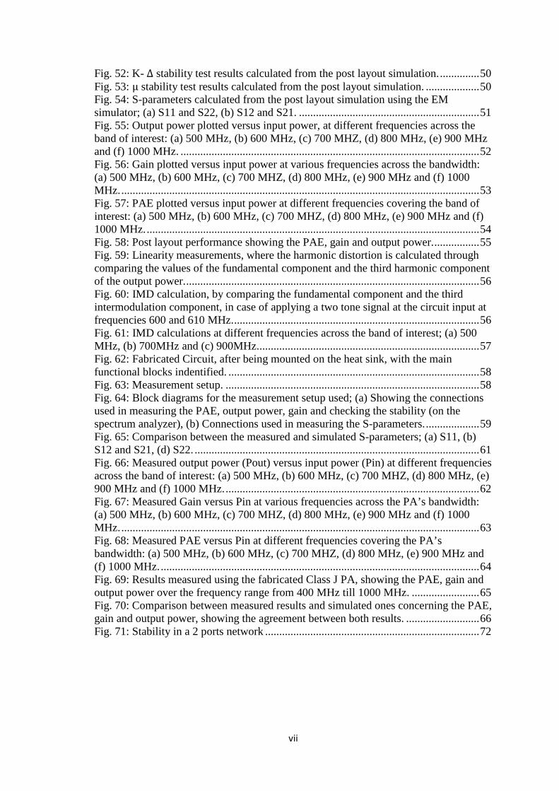
vii
Fig. 52: K- ∆ stability test results calculated from the post layout simulation. .............. 50 Fig. 53: µ stability test results calculated from the post layout simulation. ................... 50 Fig. 54: S-parameters calculated from the post layout simulation using the EM simulator; (a) S11 and S22, (b) S12 and S21. ................................................................ 51 Fig. 55: Output power plotted versus input power, at different frequencies across the band of interest: (a) 500 MHz, (b) 600 MHz, (c) 700 MHZ, (d) 800 MHz, (e) 900 MHz and (f) 1000 MHz. .......................................................................................................... 52 Fig. 56: Gain plotted versus input power at various frequencies across the bandwidth: (a) 500 MHz, (b) 600 MHz, (c) 700 MHZ, (d) 800 MHz, (e) 900 MHz and (f) 1000 MHz. ............................................................................................................................... 53 Fig. 57: PAE plotted versus input power at different frequencies covering the band of interest: (a) 500 MHz, (b) 600 MHz, (c) 700 MHZ, (d) 800 MHz, (e) 900 MHz and (f) 1000 MHz. ...................................................................................................................... 54 Fig. 58: Post layout performance showing the PAE, gain and output power. ................ 55 Fig. 59: Linearity measurements, where the harmonic distortion is calculated through comparing the values of the fundamental component and the third harmonic component of the output power. ........................................................................................................ 56 Fig. 60: IMD calculation, by comparing the fundamental component and the third intermodulation component, in case of applying a two tone signal at the circuit input at frequencies 600 and 610 MHz. ....................................................................................... 56 Fig. 61: IMD calculations at different frequencies across the band of interest; (a) 500 MHz, (b) 700MHz and (c) 900MHz. .............................................................................. 57 Fig. 62: Fabricated Circuit, after being mounted on the heat sink, with the main functional blocks indentified. ......................................................................................... 58 Fig. 63: Measurement setup. .......................................................................................... 58 Fig. 64: Block diagrams for the measurement setup used; (a) Showing the connections used in measuring the PAE, output power, gain and checking the stability (on the spectrum analyzer), (b) Connections used in measuring the S-parameters. ................... 59 Fig. 65: Comparison between the measured and simulated S-parameters; (a) S11, (b) S12 and S21, (d) S22. ..................................................................................................... 61 Fig. 66: Measured output power (Pout) versus input power (Pin) at different frequencies across the band of interest: (a) 500 MHz, (b) 600 MHz, (c) 700 MHZ, (d) 800 MHz, (e) 900 MHz and (f) 1000 MHz. .......................................................................................... 62 Fig. 67: Measured Gain versus Pin at various frequencies across the PA’s bandwidth: (a) 500 MHz, (b) 600 MHz, (c) 700 MHZ, (d) 800 MHz, (e) 900 MHz and (f) 1000 MHz. ............................................................................................................................... 63 Fig. 68: Measured PAE versus Pin at different frequencies covering the PA’s bandwidth: (a) 500 MHz, (b) 600 MHz, (c) 700 MHZ, (d) 800 MHz, (e) 900 MHz and (f) 1000 MHz. ................................................................................................................. 64 Fig. 69: Results measured using the fabricated Class J PA, showing the PAE, gain and output power over the frequency range from 400 MHz till 1000 MHz. ........................ 65 Fig. 70: Comparison between measured results and simulated ones concerning the PAE, gain and output power, showing the agreement between both results. .......................... 66 Fig. 71: Stability in a 2 ports network ............................................................................ 72

viii
List of Acronyms
BW
Bandwidth
CAD
Computer Aided Design
CR Cognitive Radio
DC Direct Current
dB
Decibel
EM
Electromagnetic
FCC Federal Communications Commission, USA
GaN
Gallium Nitride
HEMT
High Electron Mobility Transistor
IEEE Institute of Electrical and Electronics Engineers
IMD
Intermodulation Distortion
NTIA National Telecommunications and Information Administration, USA
NTRA National Telecom Regulatory Authority, Egypt
NTI National Telecommunication Institute, Egypt
PUF
Power Utilization Factor
PA
Power Amplifier
PCB
Printed Circuit Board
PAE
Power Added Efficiency
RF
Radio Frequency
SDR Software Defined Radio
SMA SubMiniature version A
TL
Transmission Line
USA United States of America

ix
List of Symbols
Cc
Coupling Capacitance
CDS
MOSFET’s Drain to source capacitance
Cp
Output Power Capability
P0
AC output power
PD
Dissipated Power
𝑉𝐺𝑆
Gate to source DC voltage
𝑣𝑔𝑠
Gate to source AC voltage
𝑣𝑔𝑠𝑚
Amplitude of the gate to source AC signal
𝑣𝐺𝑆
Gate to source total (DC and AC) voltage
𝑉𝐷𝑆
Drain to source DC voltage
𝑉𝐼
Supply Voltage
𝑉𝑡
Threshold Voltage for the MOSFET
Ѳ Conduction Angle
η Efficiency
Γ Reflection Coefficient
x
Abstract
The need for an efficient power amplifier (PA) is one of the most demanding requirements in the design process for a wide spectrum of applications nowadays. In communication systems, low operational cost and high data-handling capability are considered as cornerstones in the targeted specifications. Since a large portion of total power consumption in the system occurs at the PA stage, the strictness of the PA design specifications becomes unquestionable in order to minimize the power losses and thus improve the system performance.
Communication systems and standards undergo tremendous developments and modifications, as a result of the extensive research conducted in this field to meet the outstanding demands of the novel applications, which subsequently requires the enhancement of the initial hardware blocks that constitute such systems. Cognitive radio (CR) is one of such cutting edge technologies that have evolved as a result of such developments and needs. Yet, implementation of CR systems requires innovative design methodologies, on both the system and the components levels, so that the developed CR system can compete commercially. Such requirements are imposed as well on the PA design, requiring specific constraints to be achieved namely; wide bandwidth, high efficiency, good linearity, proved stability and high output power capabilities. In this work, after conducting an in-depth research in the available PA classes as well as new techniques suggested in the recent few years, a broadband, high efficiency Class-J PA is proposed as a part of the RF front-end of a CR system operating in the TV band, for the first time that such class is used in this band. The proposed PA design covers the frequency band from 0.4 GHz till 1 GHz, reaching a percentage bandwidth of 85.7%, which is the highest to be achieved with a Class J PA in the literature so far, and with efficiency above 60% over that whole bandwidth of operation.
1
Chapter 1 : Introduction
A power amplifier (PA) is one of the most common blocks in electronic circuits and serves in countless applications, be it industrial, military, civilian or even scientific. Such applications range from communication systems, television broadcasting, radar systems, networking, electromagnetic applications as plasma generators, laser exciters and RF heating, passing through testing passive elements, such as antennas, to active devices such as limiter diodes.
For wireless communication systems, key requirements are low operational cost and high data-handling capability. Due to the continuously increasing frequencies at which modern communication systems operate, microwave design techniques lend themselves to the design of circuits for such applications, and consequently the performance of microwave active and passive circuits in wireless communication systems has become extremely advanced. Since a large portion of the total power consumption in the system occurs at the PA stage, an efficient PA design is crucial. High efficiency guarantees lower power consumption, longer battery life, longer time-to-failure for the device, and convenient thermal management. These characteristics contribute to the reduction of the manufacturing cost and the required maintenance. As the system requirements vary, the specific constraints on the amplifier design also vary considerably. There are, however, common requirements for nearly all amplifiers, including frequency range, gain flatness, output power, linearity, matching and stability. Often there are design trade-offs required to optimize any parameter over the other, and performance compromises are usually necessary. Different classes and modes of operation were defined, each achieving certain criteria in such performance metrics. Popular examples are the basic classes such as Class A, B, C, D, E and F PAs. Because of their highly versatile circuit function, PAs have always been the first to benefit from developments in the device and semiconductor technologies, which helped in defining even new techniques for operation like the Doherty amplifiers and Class J PAs to meet the requirements imposed on PAs due to the evolution of new communication systems and standards. Among the latest emerging technologies are CR systems.
CR is a promising technology offering tremendous opportunity for providing affordable broadband wireless access to more users. Designing a CR network poses many unique challenges among which are the problems of spectrum sensing, dynamic resource allocation, ultra wideband transceivers, tight front end specifications, interference coordination… etc.
In this work, a broadband, high efficiency Class J PA is proposed as a part of the RF front-end of a CR system operating in the TV band, for the first time that such mode is used in this band. The proposed PA is designed using extensive simulations followed by prototyping to obtain high quality PCB design using low-loss substrates. The prototype is tested and the output power is measured along with the efficiency and gain. Obtained results show superior fractional bandwidth relative to other designs in the literature.
This thesis falls in six chapters. In Chapter 2, a review on CR systems and its main definitions and concepts is briefly discussed.

2
In Chapter 3, a review on PAs is presented, where a brief study of the classical classes of PAs (Classes A, B, C, D, E and F) is presented. Novel techniques in the design of PAs, as Class J, will also be examined, and the rationale behind choosing this class for the application at hand is presented.
In Chapter 4, the design proposed to reach the targeted performance will be presented. The design methodology is briefly explained, and an accurate model following such methodology is implemented on the CAD tool, and then its layout is fabricated.
Chapter 5 presents the results obtained from the designed Class J PA. The circuit model simulation results will be discussed. Afterwards, the measured results of fabricated circuit will be presented and compared with the simulated ones to verify the design.
Conclusions along with suggested future work are provided in Chapter 6.

3
Chapter 2 : Review on Cognitive Radio
In this chapter, the main definitions and concepts of CR will be briefly discussed. Capabilities and features of a CR system will be investigated as well. Afterwards, an introduction to the application at hand along with the objectives of this project will be presented.
2.1. History There were many factors that led to the development of CR technology. One of the
major drivers has been the steady increase in the demand for more radio spectrum along with a drive for improved communications and speeds. In turn this has led to initiatives to make more effective use of the spectrum, often with an associated cost dependent upon the amount of spectrum used. In addition to this, there have been many cases where greater communications diversity has been required.
With spectrum becoming a more scarce resource, many radio regulatory bodies started to look at how it might be more effectively used. CR technology [1] would lend itself to more efficient spectrum management as it would be able to utilize bands that were temporarily free and thereby maximize the use of particular bands. Similarly, others had been working on the possibility of self-configuring radios [2].
From the first glance at the radio spectrum allocation chart [3], it falsely appears as if the spectrum is fully allocated to different applications, and that a full utilization of the available spectrum is reached, yet this is not precisely true. In fact, this chart gives information about how the spectrum is “allocated” for different applications, rather than how such spectrum is really “utilized”. Therefore the need for efficient scheme for spectrum management was crucially needed, and CR stood out as a possible solution for such dilemma.
2.2. Definition Since CR is a recently developed technology [1], there is no exact definition for
what a CR is; however, there were several trials to give a general definition for a CR according to its nature. In 1999, the term CR was first defined by Joseph Mitola III and Maguire as “A radio that employs model based reasoning to achieve a specified level of competence in radio-related domains.”[1]. However, in [4], another definition for CR was introduced; “An intelligent wireless communication system that is aware of its surrounding environment (i.e., outside world), and uses the methodology of understanding-by-building to learn from the environment and adapt its internal states to statistical variations in the incoming RF stimuli by making corresponding changes in certain operating parameters (e.g., transmit-power, carrier frequency, and modulation strategy) in real-time, with two primary objectives in mind:
• Highly reliable communications whenever and wherever needed; • Efficient utilization of the radio spectrum”.
4
Coming from a background where regulations focus on the operation of transmitters, the Federal Communications Commission (FCC) [5] has defined a CR as: “A radio that can change its transmitter parameters based on interaction with the environment in which it operates.” Meanwhile, the other primary spectrum regulatory body in the USA, the National Telecommunication and Information Administration (NTIA) [6] adopted the following definition of CR that focuses on some of its applications: “A radio or system that senses its operational electromagnetic environment and can dynamically and autonomously adjust its radio operating parameters to modify system operation, such as maximize throughput, mitigate interference, facilitate interoperability, and access secondary markets.”
The IEEE tasked the IEEE 1900.1 group to define CR which has the following working definition [7]: “A type of radio that can sense and autonomously reason about its environment and adapt accordingly. This radio could employ knowledge representation, automated reasoning and machine learning mechanisms in establishing, conducting, or terminating communication or networking functions with other radios. Cognitive radios can be trained to dynamically and autonomously adjust its operating parameters.”
Likewise, the Software Defined Radio Forum (SDR) [8] participated in the FCC’s efforts to define CR and has established two groups focused on CR. The Cognitive Radio Working Group focused on identifying enabling technologies uses the following definition: “A radio that has, in some sense, awareness of changes in its environment and in response to these changes adapts its operating characteristics in some way to improve its performance or to minimize a loss in performance.”
However, the SDR Forum Special Interest Group for Cognitive Radio [8], which is developing CR applications, uses the following definition: “An adaptive, multi-dimensionally aware, autonomous radio (system) that learns from its experiences to reason, plan, and decide future actions to meet user needs.”
Finally, the Virginia Tech Cognitive Radio Working Group [9] adopted the following capability- focused definition of CR: “An adaptive radio that is capable of the following:
• Awareness of its environment and its own capabilities • Goal driven autonomous operation, • Understanding or learning how its actions impact its goal. • Recalling and correlating past actions, environments, and performance.”
However, in order to develop a satisfactory general definition for a CR system,
taking into consideration the previously mentioned trials, the capabilities of the system need to be investigated first. Consequently, the CR system can then be more generally defined according to its main functionalities that it should be capable of performing.
5
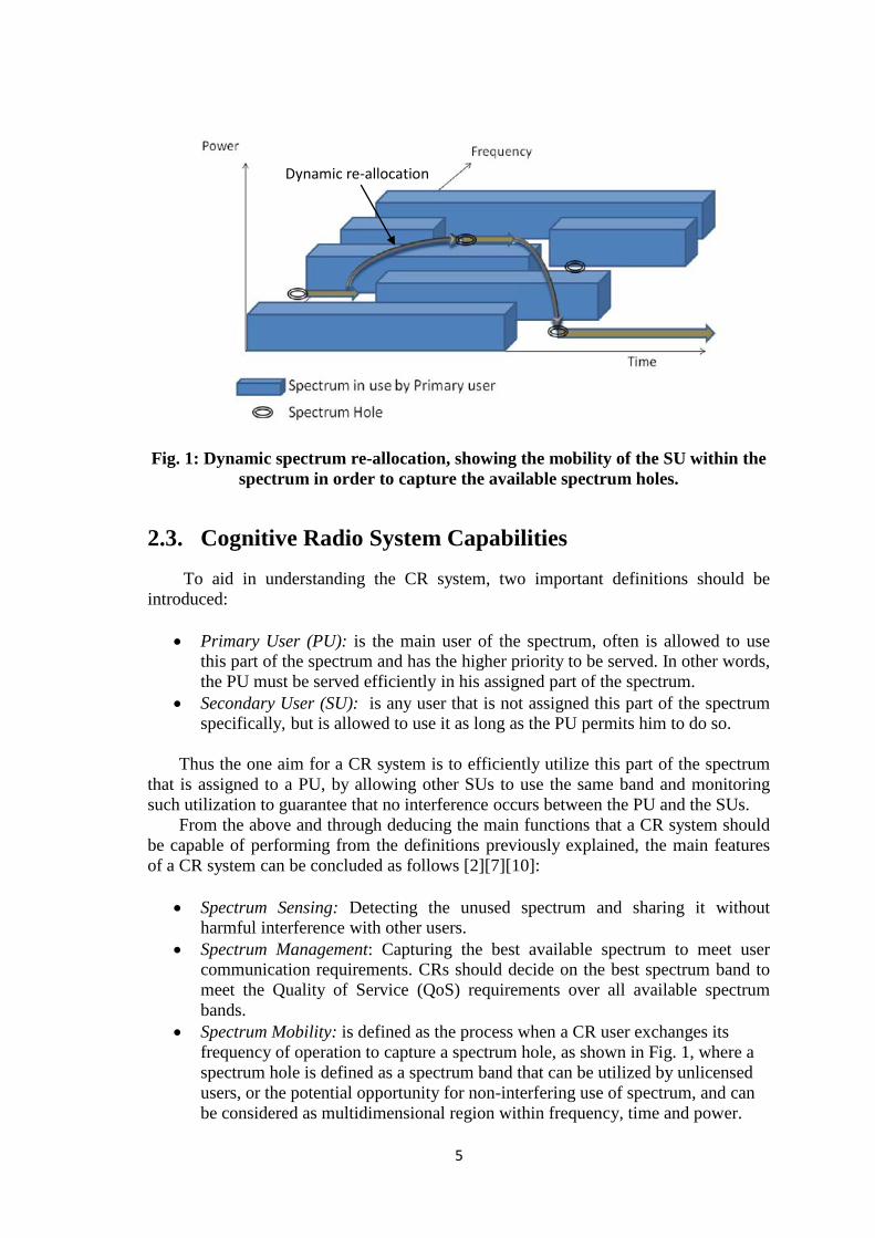
Fig. 1: Dynamic spectrum re-allocation, showing the mobility of the SU within the spectrum in order to capture the available spectrum holes.
2.3. Cognitive Radio System Capabilities To aid in understanding the CR system, two important definitions should be
introduced: • Primary User (PU): is the main user of the spectrum, often is allowed to use
this part of the spectrum and has the higher priority to be served. In other words, the PU must be served efficiently in his assigned part of the spectrum.
• Secondary User (SU): is any user that is not assigned this part of the spectrum specifically, but is allowed to use it as long as the PU permits him to do so.
Thus the one aim for a CR system is to efficiently utilize this part of the spectrum
that is assigned to a PU, by allowing other SUs to use the same band and monitoring such utilization to guarantee that no interference occurs between the PU and the SUs.
From the above and through deducing the main functions that a CR system should be capable of performing from the definitions previously explained, the main features of a CR system can be concluded as follows [2][7][10]:
• Spectrum Sensing: Detecting the unused spectrum and sharing it without harmful interference with other users.
• Spectrum Management: Capturing the best available spectrum to meet user communication requirements. CRs should decide on the best spectrum band to meet the Quality of Service (QoS) requirements over all available spectrum bands.
• Spectrum Mobility: is defined as the process when a CR user exchanges its frequency of operation to capture a spectrum hole, as shown in Fig. 1, where a spectrum hole is defined as a spectrum band that can be utilized by unlicensed users, or the potential opportunity for non-interfering use of spectrum, and can be considered as multidimensional region within frequency, time and power.
Dynamic re-allocation

6
• Spectrum Sharing: Providing the fair spectrum scheduling method to allow the SUs to co-exist.
2.4. TV Band Cognitive Radio System After the problem of efficient utilization of the available radio spectrum became obvious, the NTRA in Egypt believed in the urgency of developing novel techniques and standards to solve such problem. Expectedly, CR was one of these adopted techniques. As a part of a research project, it was decided to test the abilities of CR over a part of the TV band; mainly in the spectrum from 0.5 GHz till 1 GHz.
Objectives of this research project include studying the problems of SU access rules, and scheduling algorithms for SU access and coexistence to assist the NTRA in writing rules concerning the existence of SUs. This will include a study of the rules of SUs that exists in various parts of the world such as the power levels that can be produced by various secondary transmitters depending on the placement of broadcast stations and on the population density, e.g. urban or rural. The study will include as well whether to allow low power, e.g. portable, SUs to transmit in the same band as an existing TV channel and the relationship of this to the SUs’ location relative to a protection contour for the broadcast station.
The second track in this project is concerned with the challenges in building the RF front end; including the PA and the antenna. Most PAs are designed for a particular application and do not need to cover such a wide bandwidth, thus developing an inexpensive, efficient, and broadband PA requires adopting new design techniques, which is the scope of this thesis.
Last, an innovative antenna design based on meta-materials concepts will be considered to pave the way for sub-wavelength antennas that will cover the bandwidth.
7
Chapter 3 : Overview on Power Amplifier Technology
In this chapter a brief study of the classical classes of PAs (Classes A, B, C, D, E and F) is presented. Novel techniques in the design of PAs, namely Class J, will also be examined, and the rationale behind choosing this class for the application at hand is presented together with a review for the previously designed class-J PAs in the literature.
3.1. Historical Background The triode electronic valve was used to develop amplifier and oscillator modules,
that were associated with very limited applications and were mainly used for civil purposes, from the late 19th century to as early as 1930. However, radio communication witnessed extreme development since then, which required in return parallel enhancement in the PAs used, yet the technology was constrained at that time by the electronic valve [11-16]. A spectacular technological advancement was achieved in the early 1960s by transferring the tube-valve technology to the junction transistor technology. Amplifiers design in general thus improved due to the advance of semiconductor diodes and transistors [11-13]. Moreover, for broadband amplifier technologies, new methods and techniques for broadband matching were established [11] [14-15] [17]. All these factors helped in improving the PA performance through enhancing the efficiency, minimizing the reflections, improving the gain and increasing the percentage bandwidth that could be realized.
Classical PAs were then developed. However, the concept of obtaining a highly efficient RF amplifier by biasing the active device to a low quiescent current and allowing the RF drive signal to swing the device into conduction (used in Classes B, AB and C) is very old, dating back to the earliest days of vacuum tubes. It was assumed that all higher harmonics will be shorted at the output of the PA device. This simplifies the analysis and was a much easier condition to realize in the days of tube amplifiers. This has led to some confusion regarding the kinds of matching topologies which should be used for today’s transistor counter parts, taking into consideration the internal capacitances of the transistor. Such confusing ideas will be the pillars that recent techniques in PAs design will successfully make use of. However, approximate results have always been obtained for classical PAs through the straightforward simplified analysis explained above, thus these approximate results can be correctly used in comparison between such classes.
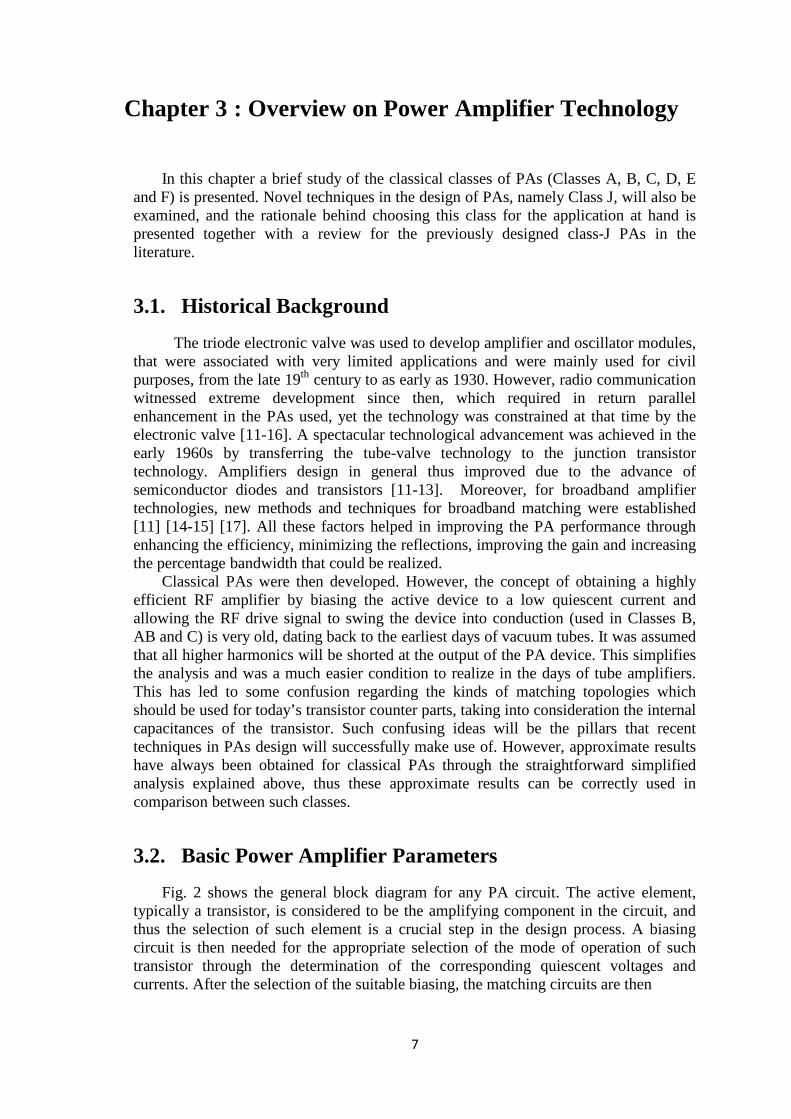
3.2. Basic Power Amplifier Parameters Fig. 2 shows the general block diagram for any PA circuit. The active element,
typically a transistor, is considered to be the amplifying component in the circuit, and thus the selection of such element is a crucial step in the design process. A biasing circuit is then needed for the appropriate selection of the mode of operation of such transistor through the determination of the corresponding quiescent voltages and currents. After the selection of the suitable biasing, the matching circuits are then
8
Fig. 2 : General block diagram, showing the main blocks that constitutes a PA circuit.
designed according the requirements of each application and mode of operation [11-12] [15].
Throughout the following review on the different classes of PAs, elementary parameters will be used to identify such classes and compare between them. These parameters are
• The Conduction Angle (2Ѳ): The portion of the input signal cycle during which the amplifying device conducts.
• Efficiency (η): The ratio of the RF output power to the DC input power. • Power Added Efficiency (PAE): The ratio of the RF output power (after
subtracting from it the RF input power) to the DC input power.
3.3. Classical Power Amplifiers Since the early development of PAs and its different applications, certain classical
modes of operation were used to identify PA circuits and their corresponding performances. From Fig. 2, it is clear that classification of PAs depends mainly on the selected quiescent point (biasing) and the nature of the matching circuits used (mainly the output matching circuit). Accordingly, the classical modes of operation for PAs were defined as follows: Group I: where the transistor acts as a dependent current source and this group includes:
• Class A • Class B • Class AB • Class C
Group II: where the transistor acts as a switch and this group includes: • Class D • Class E
And the last mode in the classical modes of PAs is Class F, which can fit in both the above groups, depending on how the transistor is operated to obtain specific output waveforms.
9
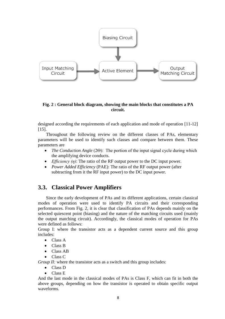
Fig. 3: DC Operating points for Classes A, B, AB and C.
Fig. 4 : Simple circuit used for the analysis of Classes A, B, AB and C, with the main PA functional blocks identified.
3.3.1. Class A, B, AB and C Power Amplifiers
In Classes A, B, AB and C PAs, the transistor is operated as a dependent current source where the DC operating point of the transistor determines the class of the amplifier, as shown from Fig. 3. Such DC biasing is realized upon the proper selection of the gate-to-source voltage (𝑉𝐺𝑠) and the corresponding drain current (𝐼𝐷) , so as to force the active element ( the transistor) to opearte in the desired mode.
Biasing Circuit
Active Element
Output Matching Circuit
10
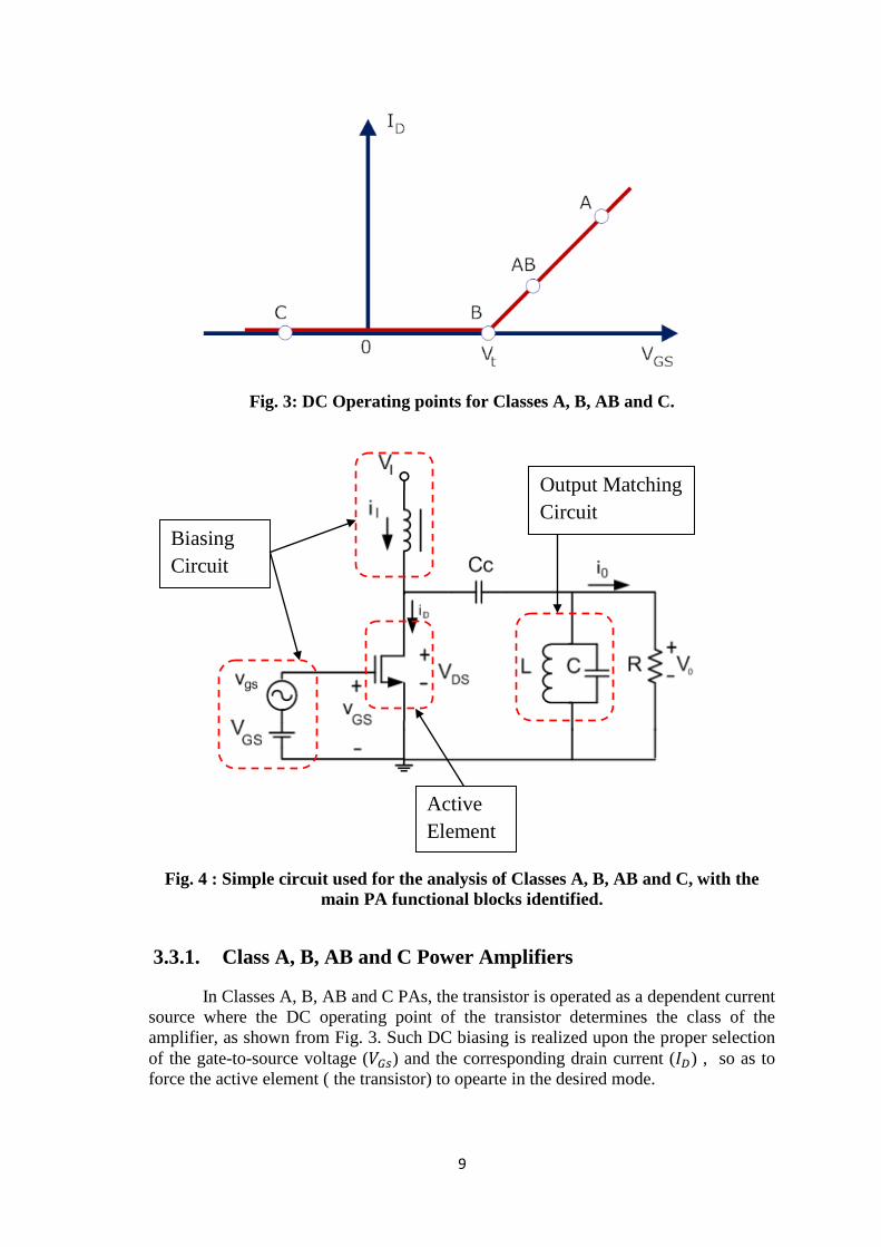
Fig. 5: Class A power amplifier wave forms [15], including the input and output voltages, drain current, output current, instantaneous output power (𝑷𝟎(𝒘𝒕)) and
the instantaneous dissipated power in the transistor (𝑷𝑫(𝒘𝒕) waveforms.
For the ease of comparison, and to properly highlight the main differences between these four modes of operation, the circuit shown in Fig. 4 will be used, where the main PA’s building blocks are clearly identified.
3.3.1.1. Class A Power Amplifiers
Where efficiency is not a consideration, most small signal linear amplifiers are designed as Class A since it is more linear and less complex than all the other types. However, a significant drawback for class A is its degraded efficiency, which is the worst among all other PAs.
11
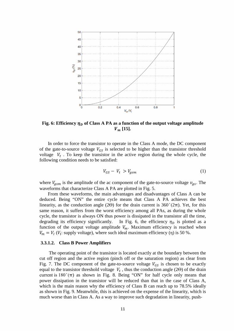
Fig. 6: Efficiency 𝜼𝑫 of Class A PA as a function of the output voltage amplitude 𝑽𝒎 [15].
In order to force the transistor to operate in the Class A mode, the DC component of the gate-to-source voltage 𝑉𝐺𝑆 is selected to be higher than the transistor threshold voltage 𝑉𝑡 . To keep the transistor in the active region during the whole cycle, the following condition needs to be satisfied:
𝑉𝐺𝑆 − 𝑉𝑡 > 𝑉𝑔𝑠𝑚 (1) where 𝑉𝑔𝑠𝑚 is the amplitude of the ac component of the gate-to-source voltage 𝑣𝑔𝑠. The waveforms that characterize Class A PA are plotted in Fig. 5.
From these waveforms, the main advantages and disadvantages of Class A can be deduced. Being “ON” the entire cycle means that Class A PA achieves the best linearity, as the conduction angle (2Ѳ) for the drain current is 360 ̊ (2π). Yet, for this same reason, it suffers from the worst efficiency among all PAs, as during the whole cycle, the transistor is always ON thus power is dissipated in the transistor all the time, degrading its efficiency significantly. In Fig. 6, the efficiency 𝜂𝐷 is plotted as a function of the output voltage amplitude 𝑉𝑚. Maximum efficiency is reached when 𝑉𝑚 = 𝑉𝐼 (𝑉I: supply voltage), where such ideal maximum efficiency (η) is 50 %.
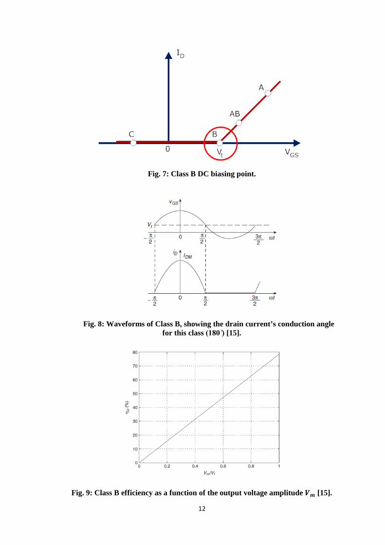
3.3.1.2. Class B Power Amplifiers
The operating point of the transistor is located exactly at the boundary between the cut off region and the active region (pinch off or the saturation region) as clear from Fig. 7. The DC component of the gate-to-source voltage 𝑉𝐺𝑆 is chosen to be exactly equal to the transistor threshold voltage 𝑉𝑡 , thus the conduction angle (2Ѳ) of the drain current is 180 ̊ (π) as shown in Fig. 8. Being “ON” for half cycle only means that power dissipation in the transistor will be reduced than that in the case of Class A, which is the main reason why the efficiency of Class B can reach up to 78.5% ideally as shown in Fig. 9. Meanwhile, this is achieved on the expense of the linearity, which is much worse than in Class A. As a way to improve such degradation in linearity, push-
12
Fig. 7: Class B DC biasing point.
Fig. 8: Waveforms of Class B, showing the drain current’s conduction angle for this class (180 ̊) [15].
Fig. 9: Class B efficiency as a function of the output voltage amplitude 𝑽𝒎 [15].

13
Fig. 10: Class C DC biasing point.
Fig. 11: Class C waveforms, showing the drain current’s conduction angle (less than 180 ̊) [15].
-pull topology can be used in Class B, but such topology may suffer from cross-over distortion, a fact which should be taken into consideration in the design process to guarantee that it will be accounted for.
3.3.1.3. Class AB Power Amplifiers
Class AB PAs emerged as a compromise between the previous two classes (A and B). The DC component of the gate-to-source voltage 𝑉𝐺𝑆 is biased at an intermediate value between classes A and B, yielding a conduction angle (2Ѳ) for the drain current between 180 ̊ (π) and 360 ̊ (2π). A tradeoff is now achieved between both linearity , which is now better than class B yet still worse than class A, and efficiency that is improved compared to class A but not as high as in the class B case.
3.3.1.4. Class C Power Amplifiers
The operating point of the transistor is located in the cut off region, as shown in Fig. 10. The DC component of the gate-to-source voltage VGS is selected to be less than the
14
Fig. 12: Block diagram for switching power amplifiers.
transistor threshold voltage Vt , leading to a conduction angle (2Ѳ) for the drain current less than 180 ̊ (π) as shown in Fig. 13, and thus improving the efficiency of this PA over Class B, yet linearity will be much degraded. Efficiency will be function in the conduction angle, which is determined in return by the DC biasing. Ideally, efficiency of a Class C PA can reach up to 100% in case of 0 ̊ (vanishing) conduction angle, which is a nonrealistic case meaning that no output would exist.
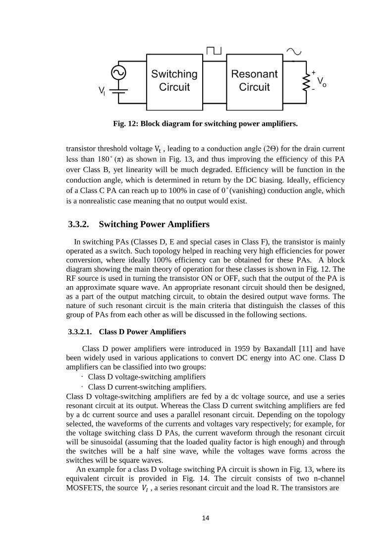
3.3.2. Switching Power Amplifiers
In switching PAs (Classes D, E and special cases in Class F), the transistor is mainly operated as a switch. Such topology helped in reaching very high efficiencies for power conversion, where ideally 100% efficiency can be obtained for these PAs. A block diagram showing the main theory of operation for these classes is shown in Fig. 12. The RF source is used in turning the transistor ON or OFF, such that the output of the PA is an approximate square wave. An appropriate resonant circuit should then be designed, as a part of the output matching circuit, to obtain the desired output wave forms. The nature of such resonant circuit is the main criteria that distinguish the classes of this group of PAs from each other as will be discussed in the following sections.
3.3.2.1. Class D Power Amplifiers
Class D power amplifiers were introduced in 1959 by Baxandall [11] and have been widely used in various applications to convert DC energy into AC one. Class D amplifiers can be classified into two groups:
• Class D voltage-switching amplifiers • Class D current-switching amplifiers.
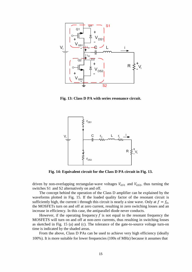
Class D voltage-switching amplifiers are fed by a dc voltage source, and use a series resonant circuit at its output. Whereas the Class D current switching amplifiers are fed by a dc current source and uses a parallel resonant circuit. Depending on the topology selected, the waveforms of the currents and voltages vary respectively; for example, for the voltage switching class D PAs, the current waveform through the resonant circuit will be sinusoidal (assuming that the loaded quality factor is high enough) and through the switches will be a half sine wave, while the voltages wave forms across the switches will be square waves. An example for a class D voltage switching PA circuit is shown in Fig. 13, where its equivalent circuit is provided in Fig. 14. The circuit consists of two n-channel MOSFETS, the source 𝑉𝐼 , a series resonant circuit and the load R. The transistors are
15
Fig. 13: Class D PA with series resonance circuit.
Fig. 14: Equivalent circuit for the Class D PA circuit in Fig. 13.
driven by non-overlapping rectangular-wave voltages 𝑉𝐺𝑆1 and 𝑉𝐺𝑆2, thus turning the switches S1 and S2 alternatively on and off.
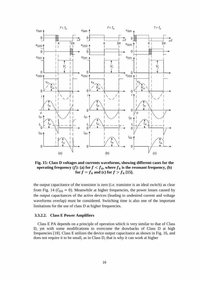
The concept behind the operation of the Class D amplifier can be explained by the waveforms plotted in Fig. 15. If the loaded quality factor of the resonant circuit is sufficiently high, the current i through this circuit is nearly a sine wave. Only at 𝑓 = 𝑓0, the MOSFETs turn on and off at zero current, resulting in zero switching losses and an increase in efficiency. In this case, the antiparallel diode never conducts.
However, if the operating frequency 𝑓 is not equal to the resonant frequency the MOSFETS will turn on and off at non-zero currents, thus resulting in switching losses as sketched in Fig. 15 (a) and (c). The tolerance of the gate-to-source voltage turn-on time is indicated by the shaded areas. From the above, Class D PAs can be used to achieve very high efficiency (ideally 100%). It is more suitable for lower frequencies (100s of MHz) because it assumes that
16
Fig. 15: Class D voltages and currents waveforms, showing different cases for the operating frequency (𝒇): (a) for 𝒇 < 𝒇𝟎, where 𝒇𝟎 is the resonant frequency, (b)
for 𝒇 = 𝒇𝟎 and (c) for 𝒇 > 𝒇𝟎 [15].
the output capacitance of the transistor is zero (i.e. transistor is an ideal switch) as clear from Fig. 14 (CDS = 0). Meanwhile at higher frequencies, the power losses caused by the output capacitances of the active devices (leading to undesired current and voltage waveforms overlap) must be considered. Switching time is also one of the important limitations for the use of class D at higher frequencies.
3.3.2.2. Class E Power Amplifiers
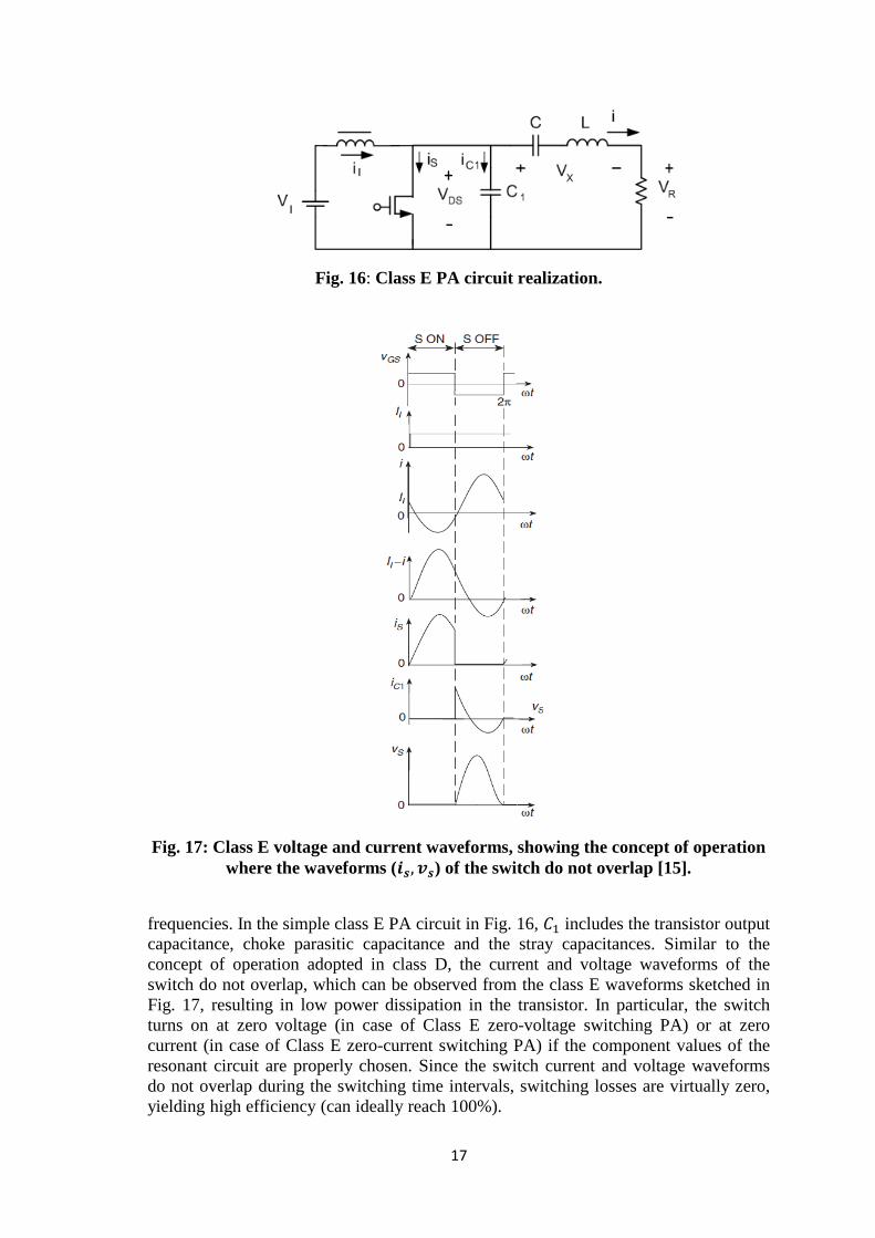
Class E PA depends on a principle of operation which is very similar to that of Class D, yet with some modifications to overcome the drawbacks of Class D at high frequencies [18]. Class E utilizes the device output capacitance as shown in Fig. 16, and does not require it to be small, as in Class D, that is why it can work at higher
17
Fig. 16: Class E PA circuit realization.
Fig. 17: Class E voltage and current waveforms, showing the concept of operation where the waveforms (𝒊𝒔,𝒗𝒔) of the switch do not overlap [15].
frequencies. In the simple class E PA circuit in Fig. 16, 𝐶1 includes the transistor output capacitance, choke parasitic capacitance and the stray capacitances. Similar to the concept of operation adopted in class D, the current and voltage waveforms of the switch do not overlap, which can be observed from the class E waveforms sketched in Fig. 17, resulting in low power dissipation in the transistor. In particular, the switch turns on at zero voltage (in case of Class E zero-voltage switching PA) or at zero current (in case of Class E zero-current switching PA) if the component values of the resonant circuit are properly chosen. Since the switch current and voltage waveforms do not overlap during the switching time intervals, switching losses are virtually zero, yielding high efficiency (can ideally reach 100%).
18
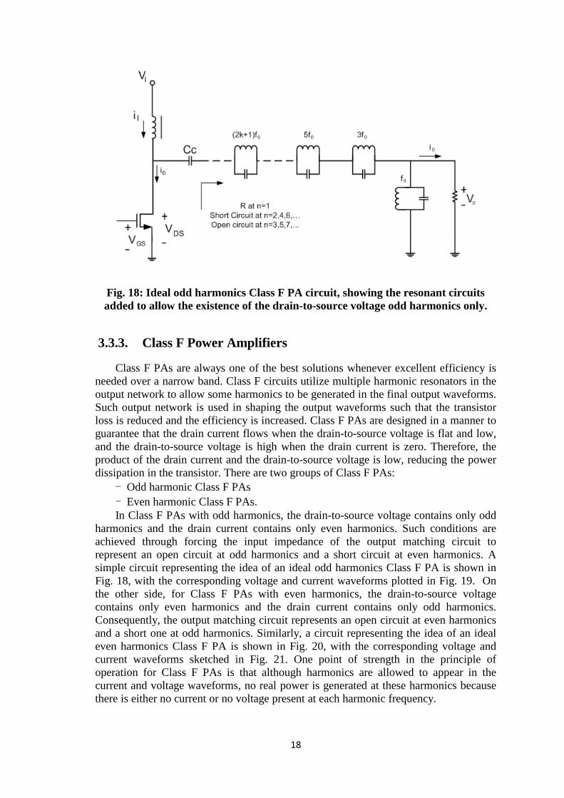
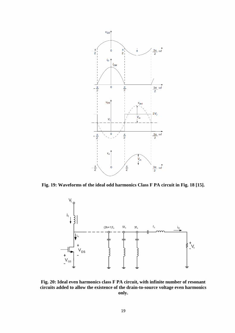
Fig. 18: Ideal odd harmonics Class F PA circuit, showing the resonant circuits added to allow the existence of the drain-to-source voltage odd harmonics only.
3.3.3. Class F Power Amplifiers
Class F PAs are always one of the best solutions whenever excellent efficiency is needed over a narrow band. Class F circuits utilize multiple harmonic resonators in the output network to allow some harmonics to be generated in the final output waveforms. Such output network is used in shaping the output waveforms such that the transistor loss is reduced and the efficiency is increased. Class F PAs are designed in a manner to guarantee that the drain current flows when the drain-to-source voltage is flat and low, and the drain-to-source voltage is high when the drain current is zero. Therefore, the product of the drain current and the drain-to-source voltage is low, reducing the power dissipation in the transistor. There are two groups of Class F PAs:
- Odd harmonic Class F PAs - Even harmonic Class F PAs. In Class F PAs with odd harmonics, the drain-to-source voltage contains only odd
harmonics and the drain current contains only even harmonics. Such conditions are achieved through forcing the input impedance of the output matching circuit to represent an open circuit at odd harmonics and a short circuit at even harmonics. A simple circuit representing the idea of an ideal odd harmonics Class F PA is shown in Fig. 18, with the corresponding voltage and current waveforms plotted in Fig. 19. On the other side, for Class F PAs with even harmonics, the drain-to-source voltage contains only even harmonics and the drain current contains only odd harmonics. Consequently, the output matching circuit represents an open circuit at even harmonics and a short one at odd harmonics. Similarly, a circuit representing the idea of an ideal even harmonics Class F PA is shown in Fig. 20, with the corresponding voltage and current waveforms sketched in Fig. 21. One point of strength in the principle of operation for Class F PAs is that although harmonics are allowed to appear in the current and voltage waveforms, no real power is generated at these harmonics because there is either no current or no voltage present at each harmonic frequency.
19
Fig. 19: Waveforms of the ideal odd harmonics Class F PA circuit in Fig. 18 [15].
Fig. 20: Ideal even harmonics class F PA circuit, with infinite number of resonant circuits added to allow the existence of the drain-to-source voltage even harmonics
only.
20
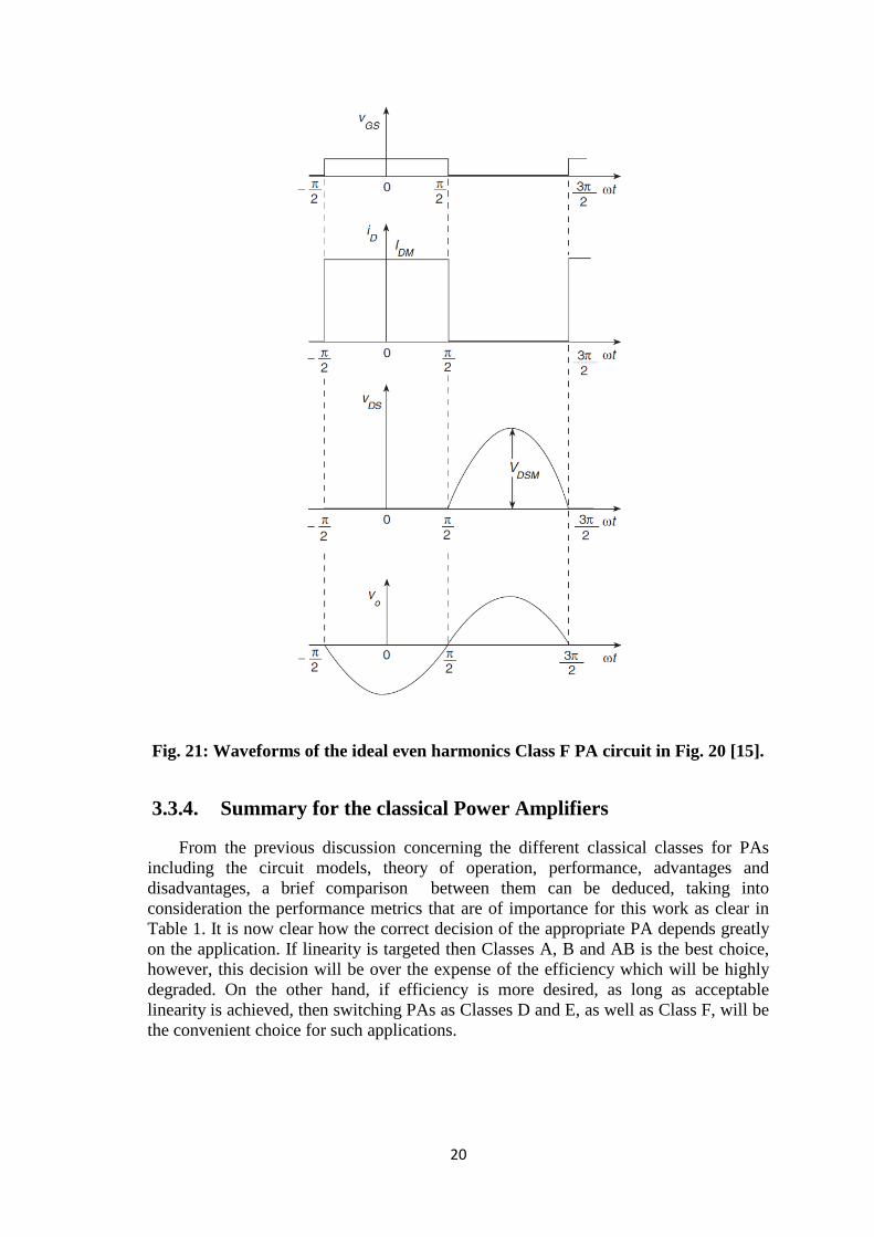
Fig. 21: Waveforms of the ideal even harmonics Class F PA circuit in Fig. 20 [15].
3.3.4. Summary for the classical Power Amplifiers
From the previous discussion concerning the different classical classes for PAs including the circuit models, theory of operation, performance, advantages and disadvantages, a brief comparison between them can be deduced, taking into consideration the performance metrics that are of importance for this work as clear in Table 1. It is now clear how the correct decision of the appropriate PA depends greatly on the application. If linearity is targeted then Classes A, B and AB is the best choice, however, this decision will be over the expense of the efficiency which will be highly degraded. On the other hand, if efficiency is more desired, as long as acceptable linearity is achieved, then switching PAs as Classes D and E, as well as Class F, will be the convenient choice for such applications.
21
Table 1: Summary for the classical modes of operation for PAs
Class Efficiency (%) Comments A 50 360 ̊ conduction angle B 78.5 180 ̊ conduction angle C 100 0 ̊ conduction angle D 100 Device operated as an ideal
switch (low frequency) E 100 Transistor output
capacitance considered F 100 Infinite number of
resonators
Bandwidth is another important requirement that would also affect the choice of the PA class. For example, broad band applications are not convenient for Class F PAs due to the complexity of the output matching (resonant) circuit that requires the presence of harmonics resonant circuits for every frequency of interest, which would increases the circuit complexity severely.
3.4. Class J Power Amplifiers For all the previously explained classes, it was always assumed that the output
matching circuit is either short at the frequencies of interest or open at the other frequencies, such that the transistor would always experience a pure resistive load at the frequencies of interest. However, some PA circuits show certain behavior that could not be explained. When load-pull systems, which will be explained later in this chapter, were used to obtain the constant contours for some performance metrics like the Power Added Efficiency (PAE), gain, output power…etc., through varying the value of the load that is connected to the transistor and calculating the performance parameters at each case, it was observed that certain loads, that were not purely resistive but had some reactive components, showed excellent performance results. Such cases were frequently observed, but not well explained and did not fit in any of the pre-defined PA classes.
Trials followed in order to find a scientific explanation for such a phenomenon hoping to utilize such explanations in the design process to make use of the achieved performance improvements. Some progress was achieved in [19-20], where the term “Harmonic Manipulations” was first introduced. It was shown that adopting some waveform engineering techniques, through allowing certain harmonic components to appear and with certain calculated ratios with respect to the fundamental component; the circuit performance can be clearly enhanced.
S. C. Cripps then made use of such observations and described Class J PA for the first time [11]. Class J was then defined as: “A mode in which the voltage has harmonic components which make it tend asymptotically towards a half-wave rectified sine-wave. This in practice can be usefully approximated by a suitably phased second harmonic component” [21].

22
Fig. 22: Class J DC biasing, being the same as Class B or deep Class AB.
Fig. 23: Class J current and voltage waveforms, showing the phase shift between both of them, as well as the existence of harmonic components [21].
3.4.1. Class J Power Amplifier features
The starting point in Class J design methodology is the linear Class B (or deep Class-AB) as shown in Fig. 22, thus, the Class J PA can be expected to have the same linear performance as a Class AB PA operating at the same conduction angle. Class J [21-28] has shown the theoretical potential of obtaining linear PAs that have the same efficiency and linearity as conventional Class AB designs but do not require a band-limiting harmonic short, instead it uses second harmonic voltage enhancement. The key difference between Class J and Class A, AB and F modes is the requirement for a reactive component at the fundamental load.

23
Yet, this new proposed PA poses an immediate problem as much as the device generates second harmonic power. Techniques such as current waveform clipping or wave-shaping the input signal have been proposed in an attempt to null the second harmonic component. The Class J approach utilizes a phase shift between the output current and voltage waveforms, as shown in Fig. 23, to render the second harmonic termination into the purely reactive regime. This enables significant possibilities into the realizable bandwidth-efficiency performance of the Class J PA.
The Class J voltage waveform engineering is realized by using appropriate passive fundamental and second harmonic terminations, whose values are usually obtained using the load-pull measurements. In this way, a higher fundamental component can significantly compensate for the loss in power implied by the reactive load.
3.4.2. Class J State of the Art Implementations
The first successful realization for a Class J PA was published in 2009 [21-22]. The design targeted the BW from 1.5 GHz till 2.5 GHz. Using a 10 W GaN HEMT in this design, and using waveform engineering techniques as well as load pull measurements, it succeeded in achieving a PAE of 60% - 70% over the band 1.4 – 2.7 GHz (percentage BW= 63.4%), with power gain between 10.2 – 12.2 dB and providing 39.5±0.5 dBm as output power.
In the same year as well, another successful realization for a Class J PA was reported [28]. This PA achieved PAE between 42 – 72% over the band 1.5 – 2.25 GHz, with gain 16-18 dB and output power of 40 – 41 dBm.
In 2010 [23], an optimized, saturated version of Class J PAs was developed using GaN HEMT as well. The PA achieved a PAE of 77.3 % at 2.14 GHz and saturated power of 40.6 dBm.
These implementations, as well as other successful realizations for Class J are summarized in Table 2.
Table 2: Summary for recent implementations for Class J
Work/Year Operating Frequency
(GHz)
Percentage BW (%) PAE (%) Gain (dB)
Output Power (dBm)
[22]/2009 1.4 – 2.7 63.4 % 60 – 70 10.2 - 12.2 39.5 ± 0.5 [28]/2009 1.5 – 2.25 40 % 42 – 72 16 – 18 40 – 41 [24]/2009 2.6 – 2.7 3.77 % 60 – 68 11.2 45 – 46 [23]/2010 2.14 ----------- 77.3 17 40.6 [26]/2011 2.3 – 2.7 16% 57 – 65 Average 15 40 – 40.79
[27]/2011 2 ----------- 64.5 at 2.13 GHz 10.7 39.7
[25]/2012 Dual band: 0.8 – 1.9 -----------
74.4 56.6 (1.75
GHz) (Drain Efficiency)
----------- ≈ 46
24
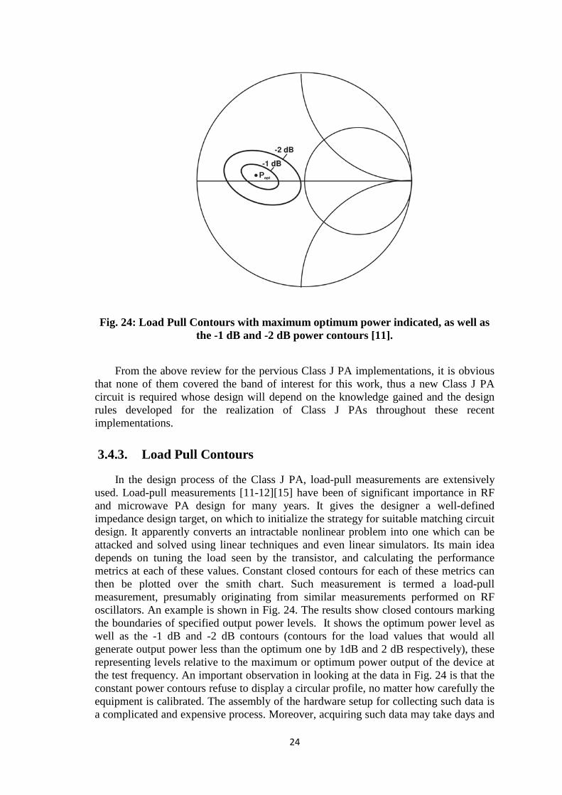
Fig. 24: Load Pull Contours with maximum optimum power indicated, as well as the -1 dB and -2 dB power contours [11].
From the above review for the pervious Class J PA implementations, it is obvious that none of them covered the band of interest for this work, thus a new Class J PA circuit is required whose design will depend on the knowledge gained and the design rules developed for the realization of Class J PAs throughout these recent implementations.
3.4.3. Load Pull Contours
In the design process of the Class J PA, load-pull measurements are extensively used. Load-pull measurements [11-12][15] have been of significant importance in RF and microwave PA design for many years. It gives the designer a well-defined impedance design target, on which to initialize the strategy for suitable matching circuit design. It apparently converts an intractable nonlinear problem into one which can be attacked and solved using linear techniques and even linear simulators. Its main idea depends on tuning the load seen by the transistor, and calculating the performance metrics at each of these values. Constant closed contours for each of these metrics can then be plotted over the smith chart. Such measurement is termed a load-pull measurement, presumably originating from similar measurements performed on RF oscillators. An example is shown in Fig. 24. The results show closed contours marking the boundaries of specified output power levels. It shows the optimum power level as well as the -1 dB and -2 dB contours (contours for the load values that would all generate output power less than the optimum one by 1dB and 2 dB respectively), these representing levels relative to the maximum or optimum power output of the device at the test frequency. An important observation in looking at the data in Fig. 24 is that the constant power contours refuse to display a circular profile, no matter how carefully the equipment is calibrated. The assembly of the hardware setup for collecting such data is a complicated and expensive process. Moreover, acquiring such data may take days and

25
weeks, thus the best realistic solution was to use load-pull wizards available on the CAD tools. Such wizards are considered a convenient solution to obtain accurate matching circuit values, to start with in the design process, without the need for the expensive hardware setup.
3.5. TV Band Power Amplifier Considering the application at hand, which is to implement a broadband PA
covering the frequency band from 0.5 GHz till 1 GHz with the best achievable compromise between the performance metrics over such bandwidth, the selection of the appropriate mode of operation turns out to be the first crucial decision. Being a part of a CR system also means that a more generic and adaptive design should be adopted to be compatible with as many applications as possible to maintain the functionalities and expected features of CR, as was deduced from its previously explained definitions.
Since linearity is one important parameter that cannot be ignored in communication systems, the first group of classes of PAs where the transistor is operated as a dependent current source appeared to be more attractive. Bearing in mind the wide bandwidth targeted, classes E and F were expected to show great complexity and difficulty in the design of the output matching circuits. And of course Class D was not recommended for such design due to the high frequency of operation (reaching 1 GHz) as well as the wide band of frequencies required, which would increase the switching losses severely in the circuit, thus losing the main advantage of Class D which is high efficiency.
It can be obviously observed that Class J, with its new promising capabilities of guaranteed high linearity being initially a Class AB PA, as well as the improved PAE, gain and output power achieved throughout the adequate selection of the output matching circuit, is the best applicable compromise for the PA required. Moreover, the nature of Class J matching circuit accounts for a broadband operation, a requirement that is given a high priority for the application at hand.
26
Chapter 4 : Proposed Class J Power Amplifier Design
The proposed design to reach the targeted performance will be presented in this chapter. The design methodology is briefly explained, and an accurate model following such methodology is implemented on the CAD tool. The final layout will then be fabricated, and tested.
4.1. Design Methodology Since the PA is generally composed of certain functional blocks, as explained in
the previous chapter, the design steps of the proposed PA will be explained for each individual block.
4.1.1. The Active Element
The most crucial block in the PA circuit is the transistor that is mainly responsible for the amplification process; therefore the proper selection of such component should be given the highest consideration. Basic points to be considered when selecting the transistor are:
• Reliability (concerning the device failure and parametric degradation) • Bandwidth • Output power capability • Stability • Thermal behavior • Availability of an accurate model on the CAD tool that will be used.
4.1.2. The Biasing Circuit
In this proposed design, it is needed to calculate the biasing voltages required to have the transistor operating as a deep Class AB PA, which is the starting point in the Class J PA design [11]. First, the behavior of the I-V characteristics of the transistor should be studied carefully. The I-V curves should be plotted at all the possible conditions (sweeping the value of one parameter as the drain to source voltage in case of a MOSFET, and plotting the drain current versus the gate to source voltage at each case). Through obtaining such data, the decision for the biasing values required can be then accurately taken, thus forcing the transistor to operate in the desired mode of operation, as explained in the previous chapter.
4.1.3. Output Matching Circuit
Biasing the transistor in the deep Class AB mode satisfies the first part of the definition of Class J PAs [21-22], explained in the previous chapter. To fulfill the other part, accurate design of the output matching circuit is a must. From the review of the implemented Class J PAs, it was clear that each work was trying to develop its unique relations to formulate the requirements of the output matching circuit that would
27
achieve the best performance. However, due to the nature of the matching circuit and the fact that it depends on the existence of a reactive part, such relations could not be directly used in this work. A case that can be explained due to two main reasons; first is the fact that such matching circuits are frequency dependent, due to the requirement of a reactive part to generate the second harmonic component used in the waveform engineering. The second reason is the physical properties of the transistor used, among which is the value of the Cds (output drain to source capacitance of the transistor), which is a crucial parameter that should be taken into consideration in the calculations of the output matching circuit design process [29]. Consequently, it was found that the best procedure to obtain accurate values for the output matching circuit needed is through using the load pull system explained in the previous chapter.
4.1.4. Input Matching Circuit
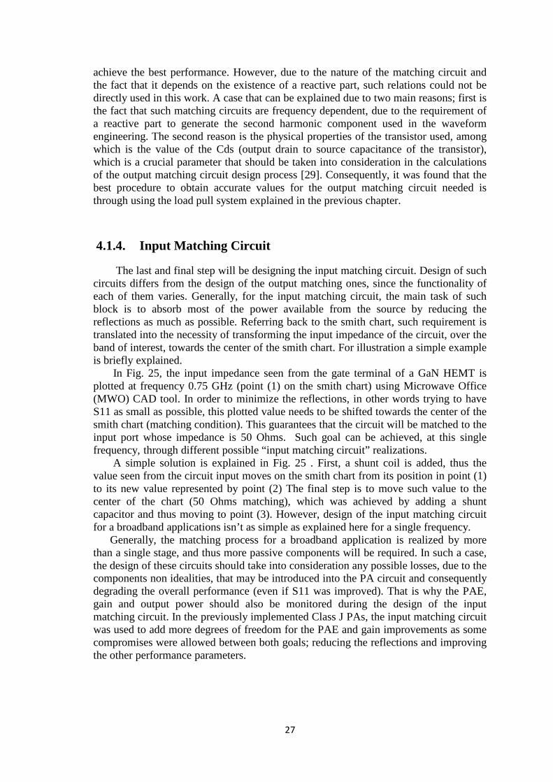
The last and final step will be designing the input matching circuit. Design of such circuits differs from the design of the output matching ones, since the functionality of each of them varies. Generally, for the input matching circuit, the main task of such block is to absorb most of the power available from the source by reducing the reflections as much as possible. Referring back to the smith chart, such requirement is translated into the necessity of transforming the input impedance of the circuit, over the band of interest, towards the center of the smith chart. For illustration a simple example is briefly explained.
In Fig. 25, the input impedance seen from the gate terminal of a GaN HEMT is plotted at frequency 0.75 GHz (point (1) on the smith chart) using Microwave Office (MWO) CAD tool. In order to minimize the reflections, in other words trying to have S11 as small as possible, this plotted value needs to be shifted towards the center of the smith chart (matching condition). This guarantees that the circuit will be matched to the input port whose impedance is 50 Ohms. Such goal can be achieved, at this single frequency, through different possible “input matching circuit” realizations.
A simple solution is explained in Fig. 25 . First, a shunt coil is added, thus the value seen from the circuit input moves on the smith chart from its position in point (1) to its new value represented by point (2) The final step is to move such value to the center of the chart (50 Ohms matching), which was achieved by adding a shunt capacitor and thus moving to point (3). However, design of the input matching circuit for a broadband applications isn’t as simple as explained here for a single frequency. Generally, the matching process for a broadband application is realized by more than a single stage, and thus more passive components will be required. In such a case, the design of these circuits should take into consideration any possible losses, due to the components non idealities, that may be introduced into the PA circuit and consequently degrading the overall performance (even if S11 was improved). That is why the PAE, gain and output power should also be monitored during the design of the input matching circuit. In the previously implemented Class J PAs, the input matching circuit was used to add more degrees of freedom for the PAE and gain improvements as some compromises were allowed between both goals; reducing the reflections and improving the other performance parameters.
28
Fig. 25: Input matching circuit design example: point (1) represents the input impedance seen from the gate terminal of the GaN HEMT at the 0.75 GHz
frequency, point (2) represents the input impedance after the addition of a shunt coil and finally point (3) represents the matched input impedance after the
addition of a shunt capacitor.
In this proposed design, the same compromise will be followed between obtaining an adequate S11 and enhancing the other performance metrics.
4.2. Power Amplifier Design Implementation The first phase in the design was to obtain an accurate model on a CAD tool to
verify the theory of operation of the PA and to monitor its performance. The assembly of such model requires in return the existence of an accurate library for the components used in the design, especially for the non-linear ones like the transistor. The CAD tool used throughout this work is the Microwave Office (MWO) CAD tool [30], provided from AWR Corporation, for being a very powerful simulation tool with the availability of both circuit simulator and EM simulator. Moreover, MWO contains an efficient and accurate library of models for a wide spectrum of commercial components, which would be of great help in the design process.
4.2.1. Selection of The Active Element
In this work, Cree CGH40010 RF Power GaN HEMT [31] will be used as the active element. GaN HEMTs are known for their high output power capabilities as well their high reliability. CGH40010 HEMT offers up to 10 watts of output power, high efficiency, high gain and wide bandwidth capabilities (up to 4 GHz, which entirely covers the whole band of interest), thus being ideal for broadband,
1
2
3

29
Fig. 26: The circuit used in MWO to determine the IV characteristics for the GaN HEMT.
linear and compressed amplifier circuits, as illustrated in Appendix A. Moreover, an accurate transistor model is available; therefore reliable results can be obtained using the CAD tools directly especially when using the load-pull wizard.
4.2.2. Class J Biasing
In order to investigate the IV characteristics of the CGH40010 GaN HEMT, the model of the HEMT was used, as shown in Fig. 26, where both 𝑉𝐺𝑆 and 𝑉𝐷𝑆 were varied over the values defined for the transistor. The drain current was thus calculated and plotted versus 𝑉𝐺𝑆 and 𝑉𝐷𝑆, as shown in Fig. 27 and Fig. 28 respectively. The quiescent point was then selected, as summarized in Table 3, to satisfy the deep Class AB mode.
Table 3: Biasing voltages selected for Class J operation
𝑉𝐺𝑆 -2.902 volts 𝑉𝐷𝑆 36 volts

30
Fig. 27: Drain current 𝑰𝑫 plotted versus the gate-to-source voltage 𝑽𝑮𝑺 (at different values for the drain-to-source voltage 𝑽𝑫𝑺 ) for the CGH40010 GaN
HEMT model.
Fig. 28 : Drain current 𝑰𝑫 plotted versus the drain-to-source voltage 𝑽𝑫𝑺 (at different values for the gate-to-source voltages 𝑽𝑮𝑺) for the CGH40010 GaN
HEMT model.
𝑉𝐷𝑆 = 10 𝑉
𝑉𝐷𝑆 = 80 𝑉
𝑉𝐺𝑆 = 1 𝑉
𝑉𝐺𝑆 = −3𝑉
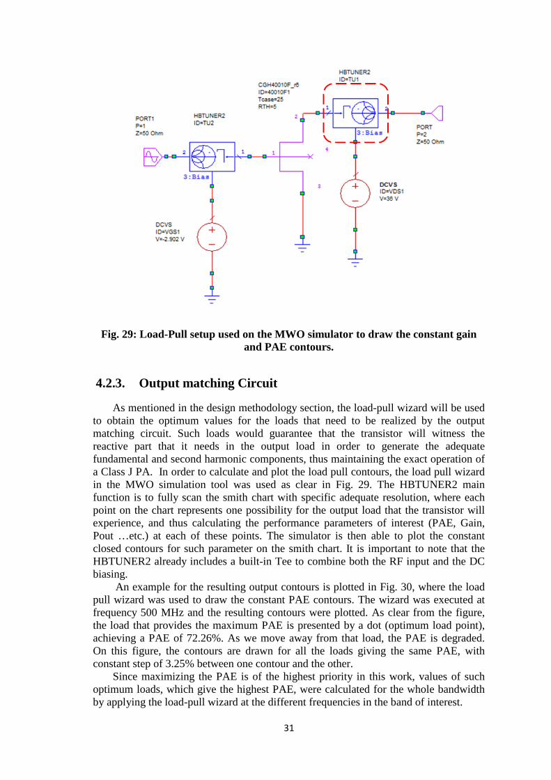
31
Fig. 29: Load-Pull setup used on the MWO simulator to draw the constant gain and PAE contours.
4.2.3. Output matching Circuit
As mentioned in the design methodology section, the load-pull wizard will be used to obtain the optimum values for the loads that need to be realized by the output matching circuit. Such loads would guarantee that the transistor will witness the reactive part that it needs in the output load in order to generate the adequate fundamental and second harmonic components, thus maintaining the exact operation of a Class J PA. In order to calculate and plot the load pull contours, the load pull wizard in the MWO simulation tool was used as clear in Fig. 29. The HBTUNER2 main function is to fully scan the smith chart with specific adequate resolution, where each point on the chart represents one possibility for the output load that the transistor will experience, and thus calculating the performance parameters of interest (PAE, Gain, Pout …etc.) at each of these points. The simulator is then able to plot the constant closed contours for such parameter on the smith chart. It is important to note that the HBTUNER2 already includes a built-in Tee to combine both the RF input and the DC biasing.
An example for the resulting output contours is plotted in Fig. 30, where the load pull wizard was used to draw the constant PAE contours. The wizard was executed at frequency 500 MHz and the resulting contours were plotted. As clear from the figure, the load that provides the maximum PAE is presented by a dot (optimum load point), achieving a PAE of 72.26%. As we move away from that load, the PAE is degraded. On this figure, the contours are drawn for all the loads giving the same PAE, with constant step of 3.25% between one contour and the other.
Since maximizing the PAE is of the highest priority in this work, values of such optimum loads, which give the highest PAE, were calculated for the whole bandwidth by applying the load-pull wizard at the different frequencies in the band of interest.

32
Fig. 30: PAE constant contours at 500 MHz, with the arrow indicating the direction of PAE increase.
Fig. 31: Required loads for achieving maximum PAE over the frequency band from 0.5 GHz till 1 GHz, calculated using the load-pull wizard.

33
Fig. 32: Constant gain contours at the 500 MHz frequency, with the arrow indicating the direction of gain increase.
The results of such sweep are shown in Fig. 31, where the optimum loads that would give the best performance concerning the PAE are plotted over the whole bandwidth. Yet, since the PAE is not the only important parameter in the PA performance, the same procedure was repeated but for maximizing the gain. The resulting contours at the 500 MHz are shown in Fig. 32.
From the above results, the first compromise needed can be easily visualized. For the ease of comparison, both the constant gain contours and the constant PAE contours are plotted, for the 500 MHz frequency on the same smith chart as shown in Fig. 33. It is obvious that the output load value that would maximize the PAE for the circuit is different from the load that would maximize the gain at the same frequency. Thus a compromise was needed. However, from the plotted constant gain contours, it is clear that the circuit would still be capable of providing high gain, even if the design process considered only the load that would maximize the PAE. Therefore, maximizing the PAE will be given the higher priority, and thus the design will be mainly based on the results obtained from the PAE load-pull wizard.
The next step was to design the output matching circuit that would realize the load values obtained from the load-pull wizard.
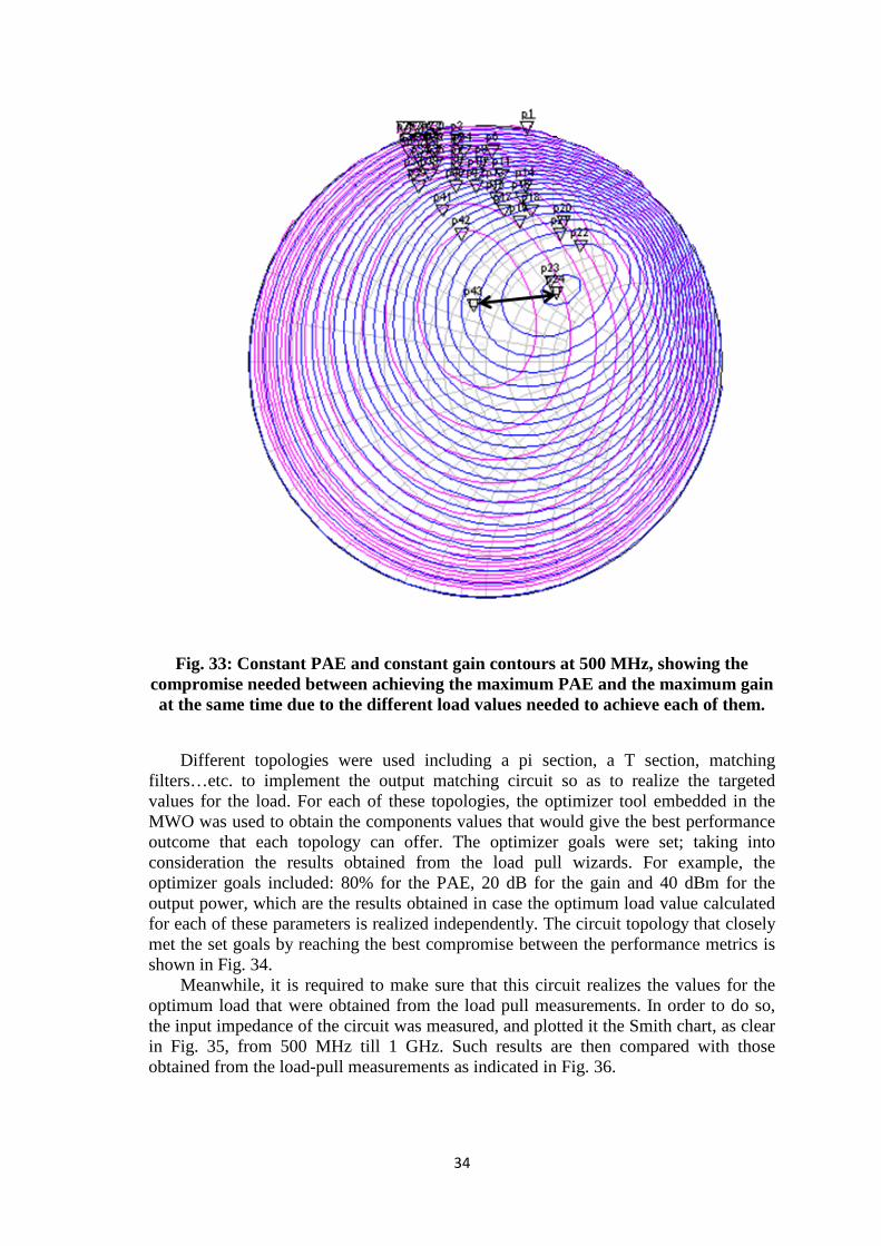
34
Fig. 33: Constant PAE and constant gain contours at 500 MHz, showing the compromise needed between achieving the maximum PAE and the maximum gain at the same time due to the different load values needed to achieve each of them.
Different topologies were used including a pi section, a T section, matching filters…etc. to implement the output matching circuit so as to realize the targeted values for the load. For each of these topologies, the optimizer tool embedded in the MWO was used to obtain the components values that would give the best performance outcome that each topology can offer. The optimizer goals were set; taking into consideration the results obtained from the load pull wizards. For example, the optimizer goals included: 80% for the PAE, 20 dB for the gain and 40 dBm for the output power, which are the results obtained in case the optimum load value calculated for each of these parameters is realized independently. The circuit topology that closely met the set goals by reaching the best compromise between the performance metrics is shown in Fig. 34.
Meanwhile, it is required to make sure that this circuit realizes the values for the optimum load that were obtained from the load pull measurements. In order to do so, the input impedance of the circuit was measured, and plotted it the Smith chart, as clear in Fig. 35, from 500 MHz till 1 GHz. Such results are then compared with those obtained from the load-pull measurements as indicated in Fig. 36.
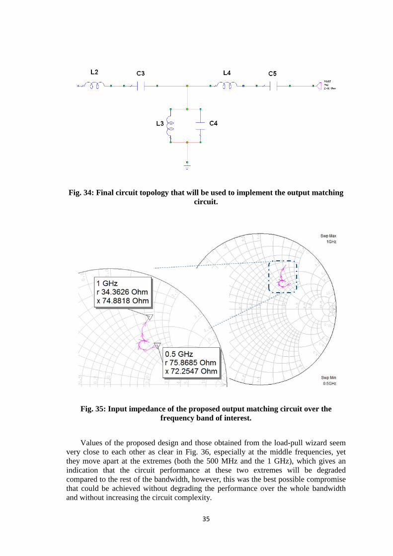
35
Fig. 34: Final circuit topology that will be used to implement the output matching circuit.
Fig. 35: Input impedance of the proposed output matching circuit over the frequency band of interest.
Values of the proposed design and those obtained from the load-pull wizard seem very close to each other as clear in Fig. 36, especially at the middle frequencies, yet they move apart at the extremes (both the 500 MHz and the 1 GHz), which gives an indication that the circuit performance at these two extremes will be degraded compared to the rest of the bandwidth, however, this was the best possible compromise that could be achieved without degrading the performance over the whole bandwidth and without increasing the circuit complexity.
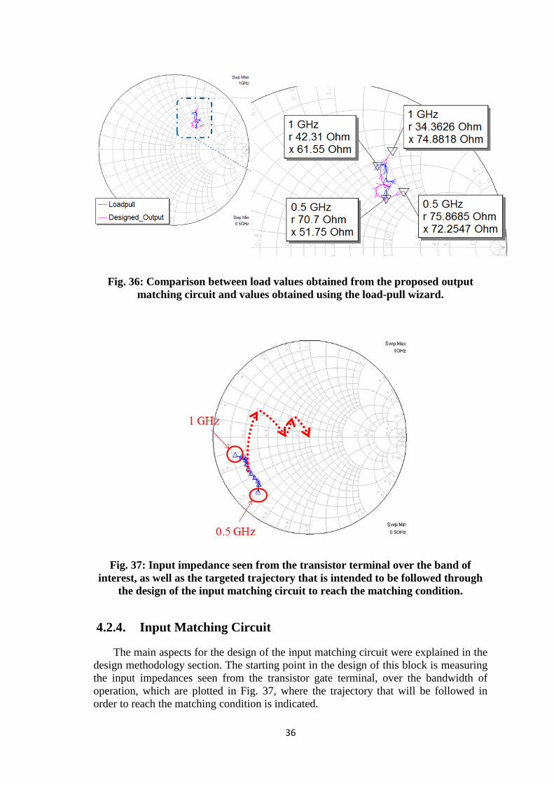
36
Fig. 36: Comparison between load values obtained from the proposed output matching circuit and values obtained using the load-pull wizard.
Fig. 37: Input impedance seen from the transistor terminal over the band of interest, as well as the targeted trajectory that is intended to be followed through
the design of the input matching circuit to reach the matching condition.
4.2.4. Input Matching Circuit
The main aspects for the design of the input matching circuit were explained in the design methodology section. The starting point in the design of this block is measuring the input impedances seen from the transistor gate terminal, over the bandwidth of operation, which are plotted in Fig. 37, where the trajectory that will be followed in order to reach the matching condition is indicated.

37
Fig. 38: Proposed input matching circuit.
Such targeted trajectory will be realized through the design of the appropriate input matching circuit. It is required to shift the input impedance values, by adding the appropriate components or transmission line transformers, to converge towards the center of the Smith chart. The proposed input matching circuit is shown in Fig. 38. First, a coupling capacitor (C2) is added to block the DC component from reaching the RF port. However, this capacitor will also be used as a part of the matching circuit to reduce the number of required components, and thus reducing the losses. The addition of C2 will push the load contour to be stretched over constant resistive circles as shown in Fig. 39 (b). Cascaded and shunt components are then added to move the load contour towards the center as shown in Fig. 39 .
It was observed that as the load contour approached the center of the Smith chart, the PAE started to degrade indicating some losses being introduced by the proposed input matching circuit. A compromise was needed between obtaining less reflections and avoiding the degradation of the overall performance. Such a compromise is represented in the shape of the final load contour that is plotted in Fig. 39 (f), which shows that, although the contour converges towards the center of the Smith chart, yet it doesn’t tightly close around the center. A fact that maintains the compromise needed between the PAE and the reflections.
The model of the microstrip lines used is shown in Fig. 40, which is the model for the substrate that will be used in the fabrication process. The selected substrate is the Rogers RO3003 RF substrate which has low loss tangent and low di-electric constant, a characteristic that would enable the fabrication of the antenna on the same substrate.
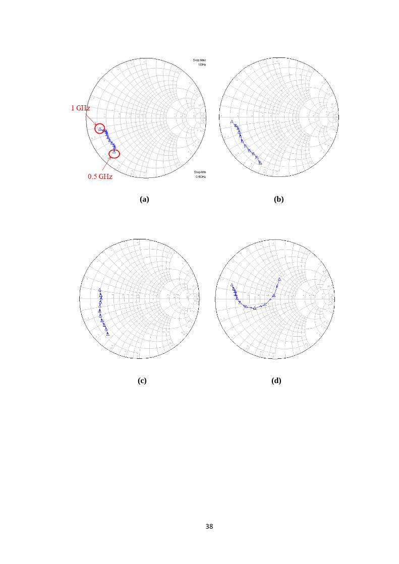
38
(a) (b)
(c) (d)
39
(e) (f)
Fig. 39: Input impedance seen over the whole bandwidth from 0.5 GHz till 1 GHz after the addition of the input matching circuit elements: (a) Input impedance seen
from the transistor’s gate, (b) after the addition of the coupling capacitor C2, (c) after inserting a resistance R1 in cascade, (d) adding the shunt inductor L1, (e)
adding a transmission line transformer TL1, (f) final input impedance seen after the addition of the shunt capacitor C1.
Fig. 40: Microstrip line model on the MWO for the Rogers RO3003 RF substrate.
40
Fig. 41: Complete Class J PA circuit model.
Now, having finished the design of the input matching circuit, the design of the four blocks of the PA circuit is thus completed and the whole PA circuit can be assembled together, as shown in Fig. 41, including the transistor model, the biasing circuits, the input and the output matching circuits.
P1 and P2 are the 50 Ohms input and output ports respectively, L5 and L6 are the RF chokes used as a part of the biasing circuits and finally C6 and C7 are the shunt capacitors used to maintain the AC ground for both the input and output matching circuits.
4.2.5. Circuit Layout and Optimization
At this point a circuit model with the fundamental circuit components only is ready; an accurate model for the circuit layout is then needed. Since the layout is the final stage in the design process, the results obtained from the layout model should resemble the measurements that are expected to be obtained from the fabricated circuit. However, there were some points that needed to be taken into consideration before designing the layout.
The first consideration was the heat generated by the GaN HEMT. Such excess heat should always be absorbed away to maintain the biasing of the transistor in the pre-defined quiescent point. The most common solution is the using a heat sink, on which the circuit should be mounted.
The second consideration was how to assemble the main circuit blocks, the input matching circuit together with the 𝑉𝐺𝑆 biasing circuit, the output matching circuit together with the 𝑉𝐷𝑆 biasing circuit and finally the transistor, whose source (lower surface as shown in Fig. 43) should be totally fixed to the ground (heat sink), to absorb any excess heat generated. There are two possibilities for the circuit design in this case. The first solution is to fabricate the input and output matching circuits solely, each on a single board then fixing the transistor between them (will appear as if floating between the two circuits), then the three parts will be mounted on the heat sink. The second solution is to design the whole circuit on a single board, and drill an adequate space in the middle to allow the transistor to be fixed on the board while still being attached to the heat sink. After considering both scenarios, it was clear that the second choice was better, to give more accurate results when using the EM simulator in the MWO tool, to
41
Fig. 42: GaN HEMT layout and dimensions [31].
take into consideration the mutual coupling effects between all the components of the circuit.
The last layout consideration was the fabrication tools resolution that would decide the minimum dimensions for the conductors, minimum distance between any two conductors, minimum drilling holes dimension …etc.
Using the Rogers R03003 model on the MWO and taking the above points into consideration, the layout design process was initiated.
Table 4: Final values for the circuit elements used
Value Component ID Value Component ID
3.9 pF C1 10 Ohms R1
18 pF C2 10 Ohms R2
100 pF C3 10 Ohms R3
3 pF C4 3.3 nH L1
3.9 pF C5 10 nH L2
100 pF C6 5.6 nH L3
100 pF C7 6.8 nH L4
L = 8.8 mm,
W = 1.3 mm TL1
390 nH L5
200 nH L6
42
Fig. 43: Input matching layout circuit schematic.
Fig. 44: Output matching layout circuit schematic.
After adding microstrip lines required for the layout design, the values of the input and output matching circuits’ components were slightly tuned to account for the undesired effects introduced to the PA circuit due to these newly added microstrip lines.
The final input and output matching circuits are shown in Fig. 43 and Fig. 44 respectively. The final values for the circuit elements are given in Table 4, whereas the whole PA circuit schematic is shown in Fig. 45. The final layout is then shown in Fig. 46.

43
Fig. 45: Final circuit Schematic.

44
Fig. 46: Final layout Design.
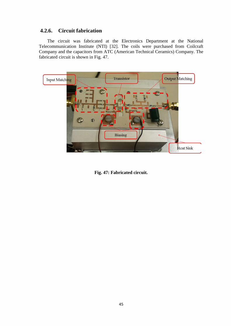
45
4.2.6. Circuit fabrication
The circuit was fabricated at the Electronics Department at the National Telecommunication Institute (NTI) [32]. The coils were purchased from Coilcraft Company and the capacitors from ATC (American Technical Ceramics) Company. The fabricated circuit is shown in Fig. 47.
Fig. 47: Fabricated circuit.
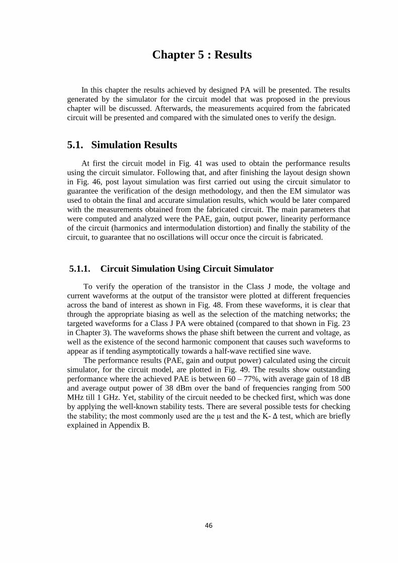
46
Chapter 5 : Results
In this chapter the results achieved by designed PA will be presented. The results generated by the simulator for the circuit model that was proposed in the previous chapter will be discussed. Afterwards, the measurements acquired from the fabricated circuit will be presented and compared with the simulated ones to verify the design.
5.1. Simulation Results At first the circuit model in Fig. 41 was used to obtain the performance results
using the circuit simulator. Following that, and after finishing the layout design shown in Fig. 46, post layout simulation was first carried out using the circuit simulator to guarantee the verification of the design methodology, and then the EM simulator was used to obtain the final and accurate simulation results, which would be later compared with the measurements obtained from the fabricated circuit. The main parameters that were computed and analyzed were the PAE, gain, output power, linearity performance of the circuit (harmonics and intermodulation distortion) and finally the stability of the circuit, to guarantee that no oscillations will occur once the circuit is fabricated.
5.1.1. Circuit Simulation Using Circuit Simulator
To verify the operation of the transistor in the Class J mode, the voltage and current waveforms at the output of the transistor were plotted at different frequencies across the band of interest as shown in Fig. 48. From these waveforms, it is clear that through the appropriate biasing as well as the selection of the matching networks; the targeted waveforms for a Class J PA were obtained (compared to that shown in Fig. 23 in Chapter 3). The waveforms shows the phase shift between the current and voltage, as well as the existence of the second harmonic component that causes such waveforms to appear as if tending asymptotically towards a half-wave rectified sine wave.
The performance results (PAE, gain and output power) calculated using the circuit simulator, for the circuit model, are plotted in Fig. 49. The results show outstanding performance where the achieved PAE is between 60 – 77%, with average gain of 18 dB and average output power of 38 dBm over the band of frequencies ranging from 500 MHz till 1 GHz. Yet, stability of the circuit needed to be checked first, which was done by applying the well-known stability tests. There are several possible tests for checking the stability; the most commonly used are the μ test and the K- ∆ test, which are briefly explained in Appendix B.
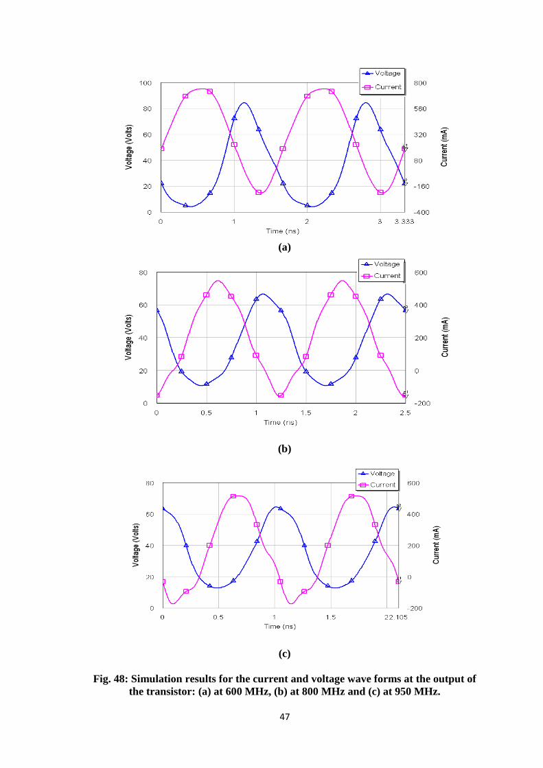
47
(a)
(b)
(c)
Fig. 48: Simulation results for the current and voltage wave forms at the output of the transistor: (a) at 600 MHz, (b) at 800 MHz and (c) at 950 MHz.
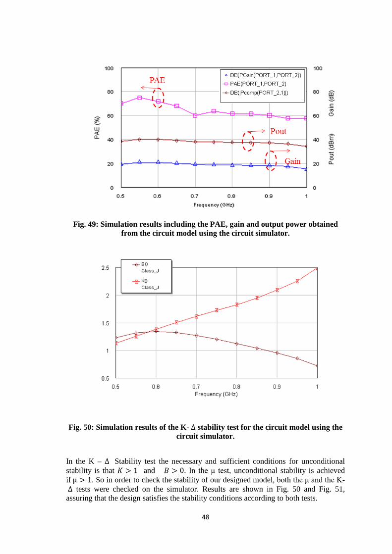
48
Fig. 49: Simulation results including the PAE, gain and output power obtained from the circuit model using the circuit simulator.
Fig. 50: Simulation results of the K- ∆ stability test for the circuit model using the circuit simulator.
In the K – ∆ Stability test the necessary and sufficient conditions for unconditional stability is that 𝐾 > 1 and 𝐵 > 0. In the μ test, unconditional stability is achieved if µ > 1. So in order to check the stability of our designed model, both the μ and the K- ∆ tests were checked on the simulator. Results are shown in Fig. 50 and Fig. 51, assuring that the design satisfies the stability conditions according to both tests.
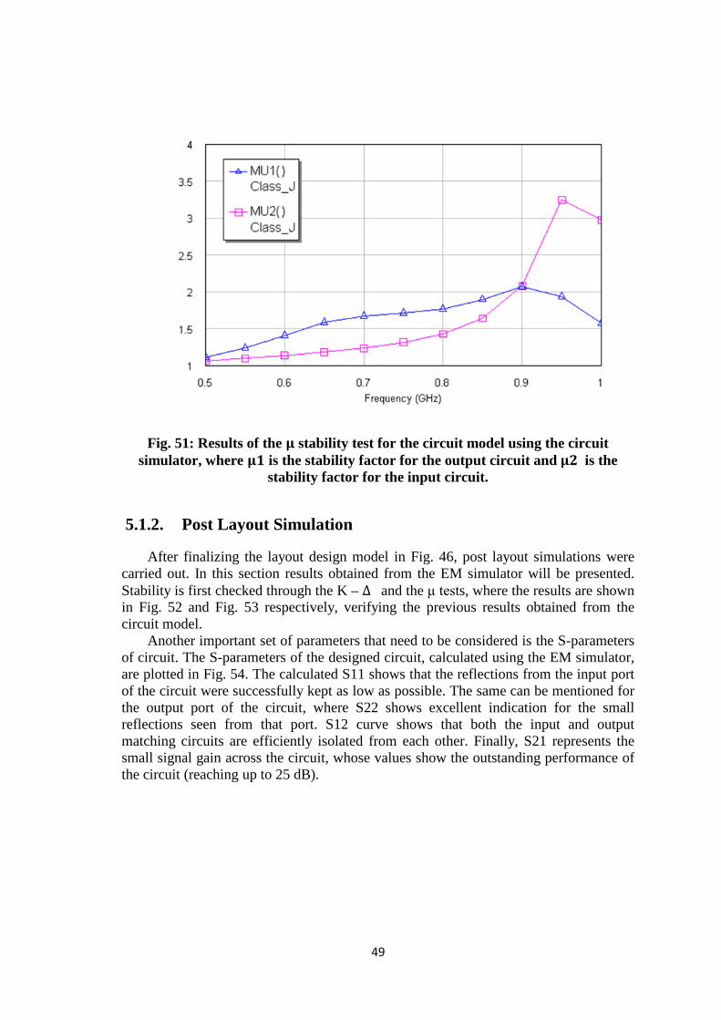
49
Fig. 51: Results of the 𝛍 stability test for the circuit model using the circuit simulator, where 𝛍𝟏 is the stability factor for the output circuit and 𝛍𝟐 is the
stability factor for the input circuit.
5.1.2. Post Layout Simulation
After finalizing the layout design model in Fig. 46, post layout simulations were carried out. In this section results obtained from the EM simulator will be presented. Stability is first checked through the K – ∆ and the μ tests, where the results are shown in Fig. 52 and Fig. 53 respectively, verifying the previous results obtained from the circuit model.
Another important set of parameters that need to be considered is the S-parameters of circuit. The S-parameters of the designed circuit, calculated using the EM simulator, are plotted in Fig. 54. The calculated S11 shows that the reflections from the input port of the circuit were successfully kept as low as possible. The same can be mentioned for the output port of the circuit, where S22 shows excellent indication for the small reflections seen from that port. S12 curve shows that both the input and output matching circuits are efficiently isolated from each other. Finally, S21 represents the small signal gain across the circuit, whose values show the outstanding performance of the circuit (reaching up to 25 dB).
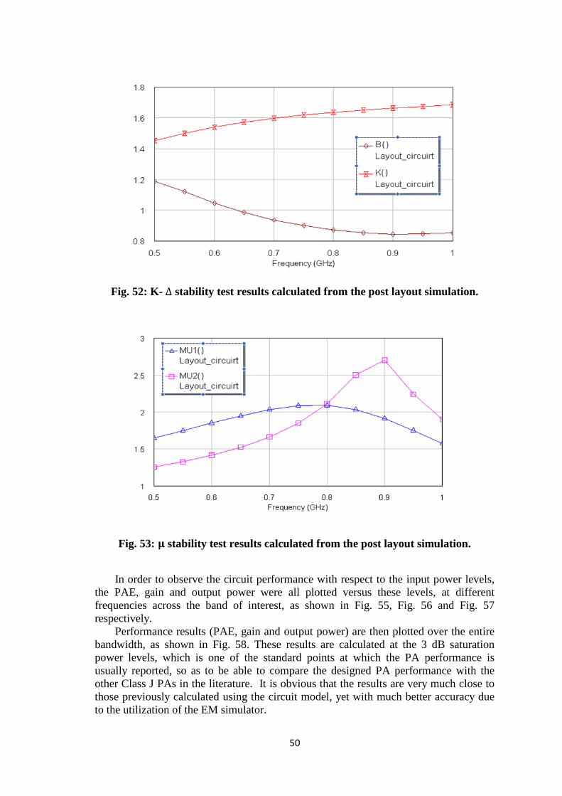
50
Fig. 52: K- ∆ stability test results calculated from the post layout simulation.
Fig. 53: 𝛍 stability test results calculated from the post layout simulation.
In order to observe the circuit performance with respect to the input power levels, the PAE, gain and output power were all plotted versus these levels, at different frequencies across the band of interest, as shown in Fig. 55, Fig. 56 and Fig. 57 respectively.
Performance results (PAE, gain and output power) are then plotted over the entire bandwidth, as shown in Fig. 58. These results are calculated at the 3 dB saturation power levels, which is one of the standard points at which the PA performance is usually reported, so as to be able to compare the designed PA performance with the other Class J PAs in the literature. It is obvious that the results are very much close to those previously calculated using the circuit model, yet with much better accuracy due to the utilization of the EM simulator.
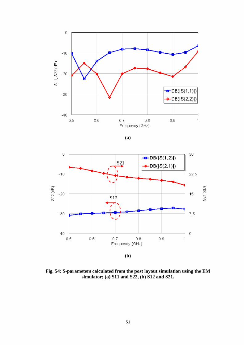
51
(a)
(b)
Fig. 54: S-parameters calculated from the post layout simulation using the EM simulator; (a) S11 and S22, (b) S12 and S21.
S21
S12
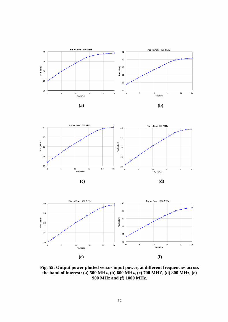
52
(a) (b)
(c) (d)
(e) (f)
Fig. 55: Output power plotted versus input power, at different frequencies across the band of interest: (a) 500 MHz, (b) 600 MHz, (c) 700 MHZ, (d) 800 MHz, (e)
900 MHz and (f) 1000 MHz.
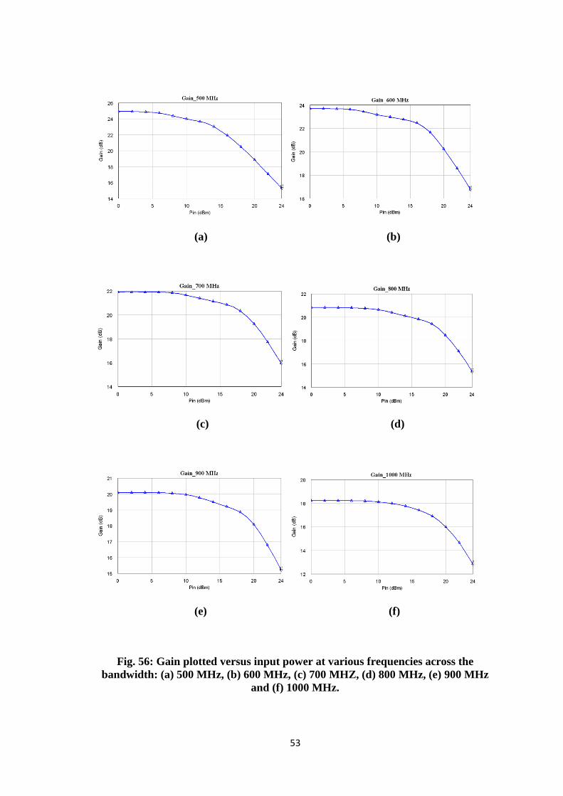
53
(a) (b)
(c) (d)
(e) (f)
Fig. 56: Gain plotted versus input power at various frequencies across the bandwidth: (a) 500 MHz, (b) 600 MHz, (c) 700 MHZ, (d) 800 MHz, (e) 900 MHz
and (f) 1000 MHz.
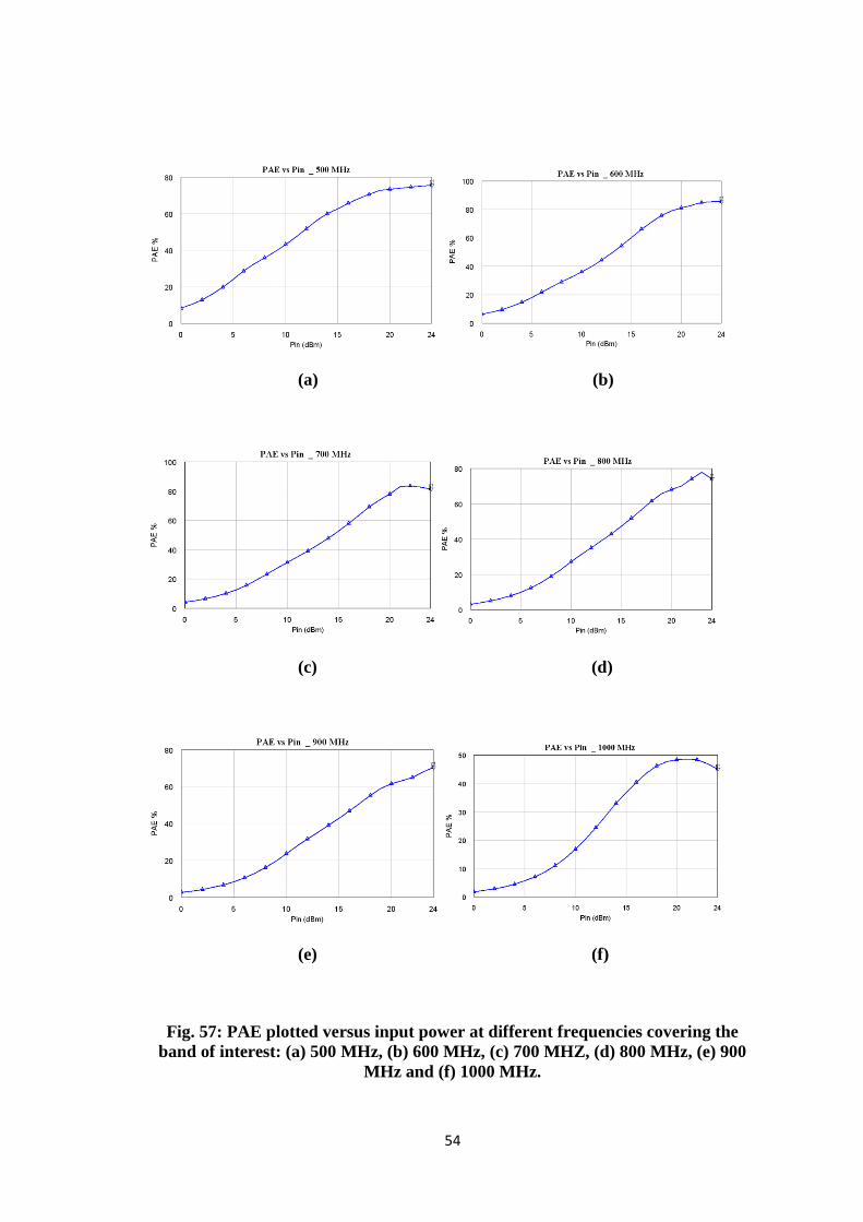
54
(a) (b)
(c) (d)
(e) (f)
Fig. 57: PAE plotted versus input power at different frequencies covering the band of interest: (a) 500 MHz, (b) 600 MHz, (c) 700 MHZ, (d) 800 MHz, (e) 900
MHz and (f) 1000 MHz.
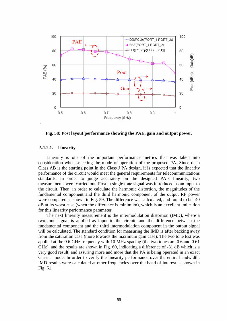
55
Fig. 58: Post layout performance showing the PAE, gain and output power.
5.1.2.1. Linearity
Linearity is one of the important performance metrics that was taken into consideration when selecting the mode of operation of the proposed PA. Since deep Class AB is the starting point in the Class J PA design, it is expected that the linearity performance of the circuit would meet the general requirements for telecommunications standards. In order to judge accurately on the designed PA’s linearity, two measurements were carried out. First, a single tone signal was introduced as an input to the circuit. Then, in order to calculate the harmonic distortion, the magnitudes of the fundamental component and the third harmonic component of the output RF power were compared as shown in Fig. 59. The difference was calculated, and found to be -40 dB at its worst case (when the difference is minimum), which is an excellent indication for this linearity performance parameter.
The next linearity measurement is the intermodulation distortion (IMD), where a two tone signal is applied as input to the circuit, and the difference between the fundamental component and the third intermodulation component in the output signal will be calculated. The standard condition for measuring the IMD is after backing away from the saturation case (more towards the maximum gain case). The two tone test was applied at the 0.6 GHz frequency with 10 MHz spacing (the two tones are 0.6 and 0.61 GHz), and the results are shown in Fig. 60, indicating a difference of -31 dB which is a very good result, and assuring more and more that the PA is being operated in an exact Class J mode. In order to verify the linearity performance over the entire bandwidth, IMD results were calculated at other frequencies over the band of interest as shown in Fig. 61.

56
Fig. 59: Linearity measurements, where the harmonic distortion is calculated through comparing the values of the fundamental component and the third
harmonic component of the output power.
Fig. 60: IMD calculation, by comparing the fundamental component and the third intermodulation component, in case of applying a two tone signal at the circuit
input at frequencies 600 and 610 MHz.
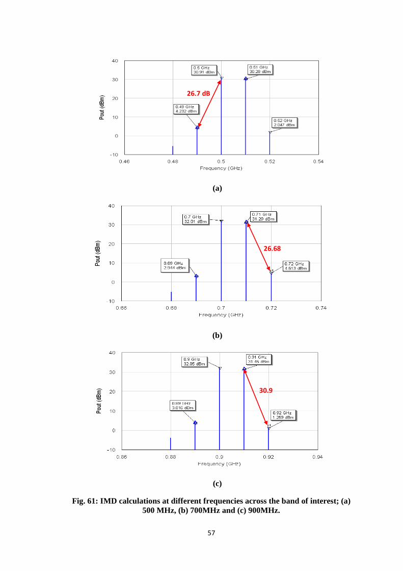
57
(a)
(b)
(c)
Fig. 61: IMD calculations at different frequencies across the band of interest; (a) 500 MHz, (b) 700MHz and (c) 900MHz.
30.9
26.7 dB
26.68

58
Fig. 62: Fabricated Circuit, after being mounted on the heat sink, with the main functional blocks indentified.
Fig. 63: Measurement setup.
5.2. Experimental Results The layout design for the proposed PA was then fabricated as shown in Fig. 62. In
order to verify the results obtained from the simulations, the parameters of interest need to be measured directly from the fabricated circuit and compared with the simulation results. The measurement setup used is shown in Fig. 63, which includes the dc supplies, the power meter to measure the input and output power levels, the network analyzer to compute the S-parameters for the fabricated circuit and finally the signal generator.
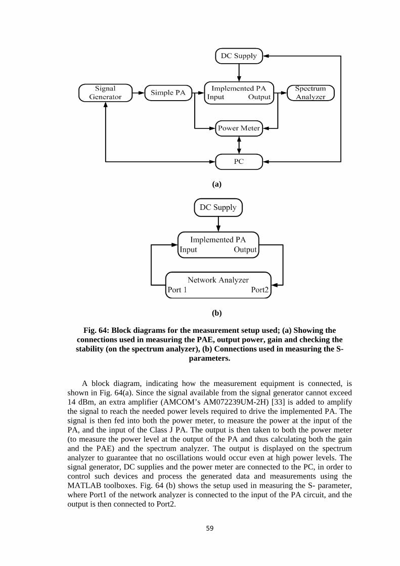
59
(a)
(b)
Fig. 64: Block diagrams for the measurement setup used; (a) Showing the connections used in measuring the PAE, output power, gain and checking the stability (on the spectrum analyzer), (b) Connections used in measuring the S-
parameters.
A block diagram, indicating how the measurement equipment is connected, is shown in Fig. 64(a). Since the signal available from the signal generator cannot exceed 14 dBm, an extra amplifier (AMCOM’s AM072239UM-2H) [33] is added to amplify the signal to reach the needed power levels required to drive the implemented PA. The signal is then fed into both the power meter, to measure the power at the input of the PA, and the input of the Class J PA. The output is then taken to both the power meter (to measure the power level at the output of the PA and thus calculating both the gain and the PAE) and the spectrum analyzer. The output is displayed on the spectrum analyzer to guarantee that no oscillations would occur even at high power levels. The signal generator, DC supplies and the power meter are connected to the PC, in order to control such devices and process the generated data and measurements using the MATLAB toolboxes. Fig. 64 (b) shows the setup used in measuring the S- parameter, where Port1 of the network analyzer is connected to the input of the PA circuit, and the output is then connected to Port2.
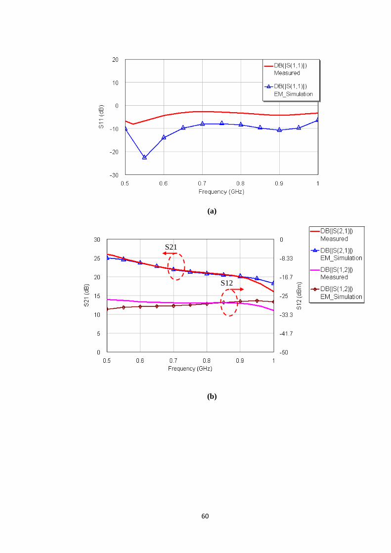
60
(a)
(b)
S21
S12
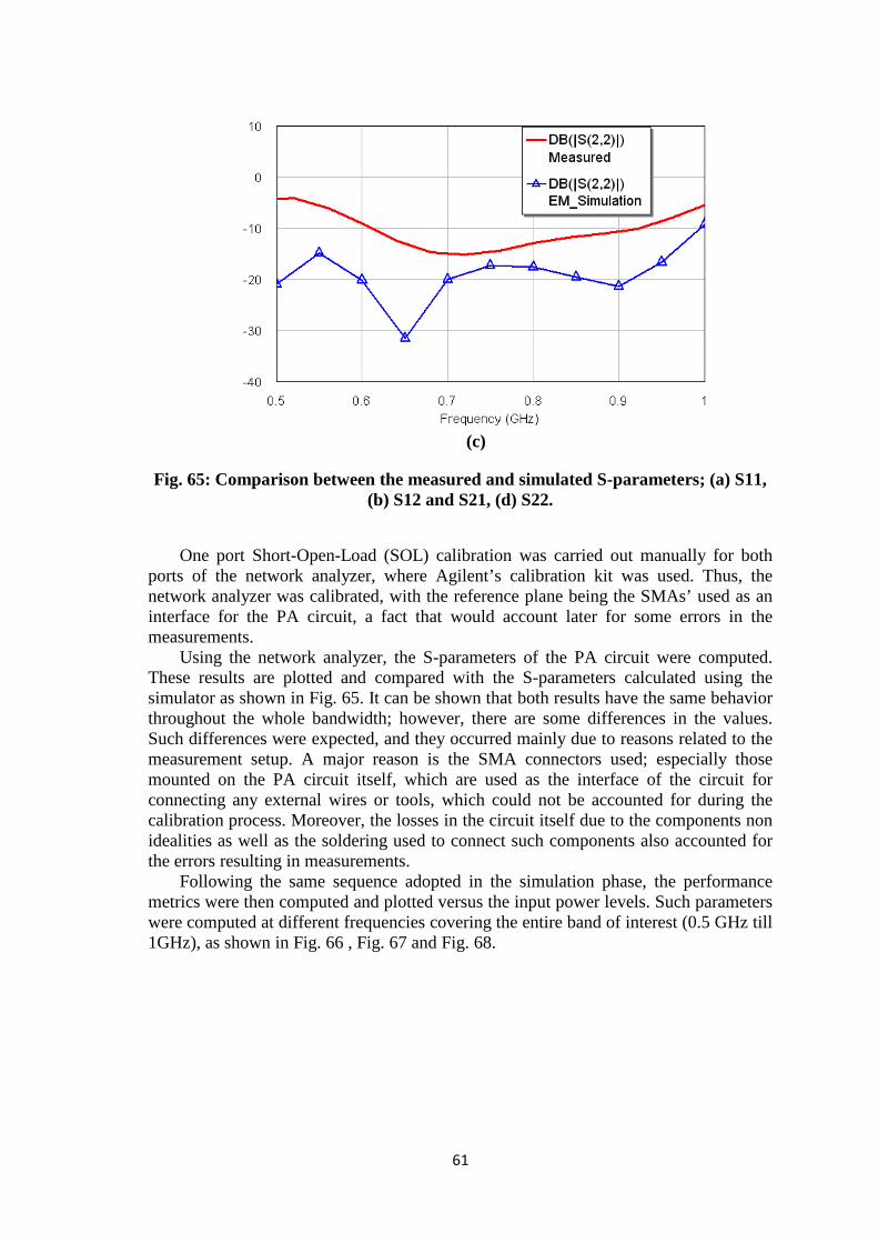
61
(c)
Fig. 65: Comparison between the measured and simulated S-parameters; (a) S11, (b) S12 and S21, (d) S22.
One port Short-Open-Load (SOL) calibration was carried out manually for both ports of the network analyzer, where Agilent’s calibration kit was used. Thus, the network analyzer was calibrated, with the reference plane being the SMAs’ used as an interface for the PA circuit, a fact that would account later for some errors in the measurements.
Using the network analyzer, the S-parameters of the PA circuit were computed. These results are plotted and compared with the S-parameters calculated using the simulator as shown in Fig. 65. It can be shown that both results have the same behavior throughout the whole bandwidth; however, there are some differences in the values. Such differences were expected, and they occurred mainly due to reasons related to the measurement setup. A major reason is the SMA connectors used; especially those mounted on the PA circuit itself, which are used as the interface of the circuit for connecting any external wires or tools, which could not be accounted for during the calibration process. Moreover, the losses in the circuit itself due to the components non idealities as well as the soldering used to connect such components also accounted for the errors resulting in measurements.
Following the same sequence adopted in the simulation phase, the performance metrics were then computed and plotted versus the input power levels. Such parameters were computed at different frequencies covering the entire band of interest (0.5 GHz till 1GHz), as shown in Fig. 66 , Fig. 67 and Fig. 68.
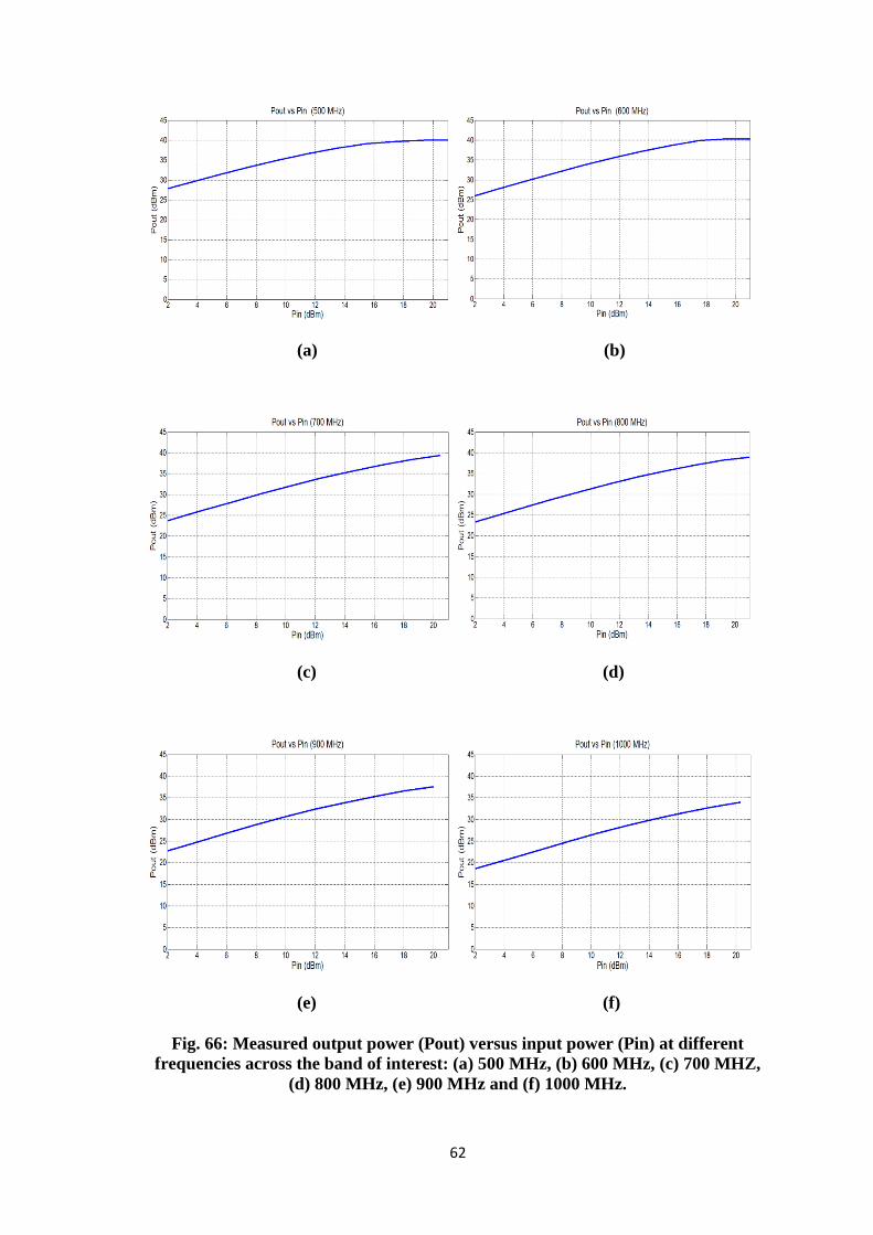
62
(a) (b)
(c) (d)
(e) (f)
Fig. 66: Measured output power (Pout) versus input power (Pin) at different frequencies across the band of interest: (a) 500 MHz, (b) 600 MHz, (c) 700 MHZ,
(d) 800 MHz, (e) 900 MHz and (f) 1000 MHz.
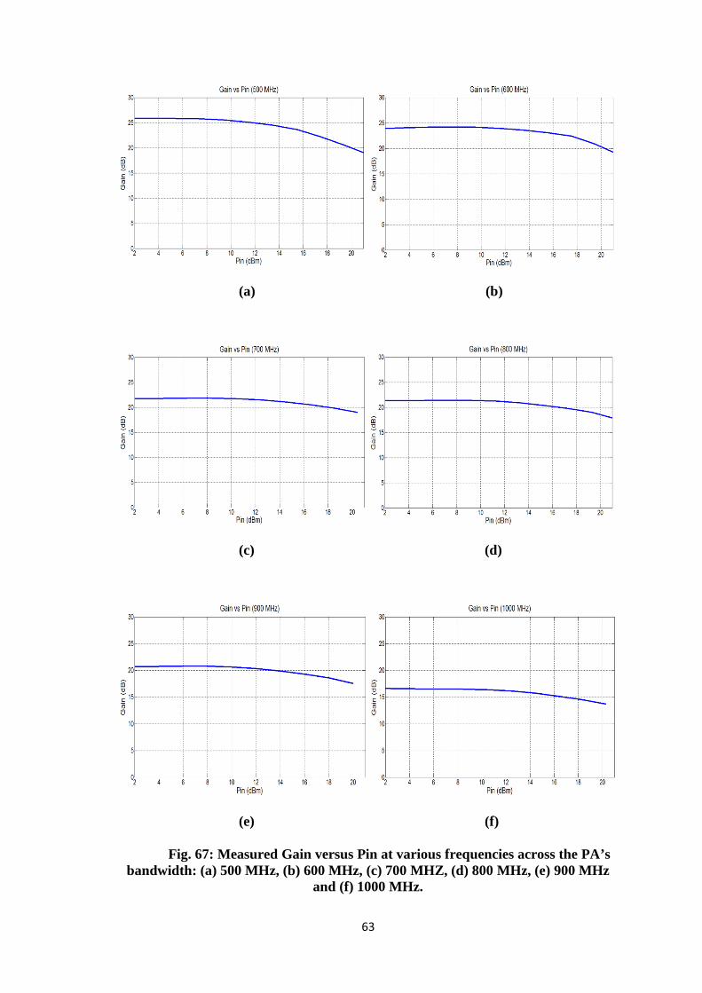
63
(a) (b)
(c) (d)
(e) (f)
Fig. 67: Measured Gain versus Pin at various frequencies across the PA’s bandwidth: (a) 500 MHz, (b) 600 MHz, (c) 700 MHZ, (d) 800 MHz, (e) 900 MHz
and (f) 1000 MHz.
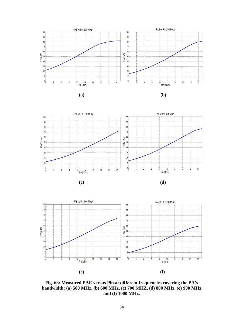
64
(a) (b)
(c) (d)
(e) (f)
Fig. 68: Measured PAE versus Pin at different frequencies covering the PA’s bandwidth: (a) 500 MHz, (b) 600 MHz, (c) 700 MHZ, (d) 800 MHz, (e) 900 MHz
and (f) 1000 MHz.
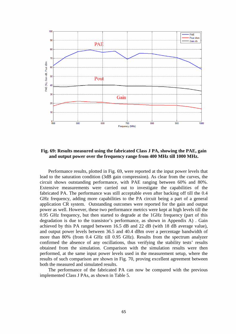
65
Fig. 69: Results measured using the fabricated Class J PA, showing the PAE, gain and output power over the frequency range from 400 MHz till 1000 MHz.
Performance results, plotted in Fig. 69, were reported at the input power levels that lead to the saturation condition (3dB gain compression). As clear from the curves, the circuit shows outstanding performance, with PAE ranging between 60% and 80%. Extensive measurements were carried out to investigate the capabilities of the fabricated PA. The performance was still acceptable even after backing off till the 0.4 GHz frequency, adding more capabilities to the PA circuit being a part of a general application CR system. Outstanding outcomes were reported for the gain and output power as well. However, these two performance metrics were kept at high levels till the 0.95 GHz frequency, but then started to degrade at the 1GHz frequency (part of this degradation is due to the transistor’s performance, as shown in Appendix A) . Gain achieved by this PA ranged between 16.5 dB and 22 dB (with 18 dB average value), and output power levels between 36.5 and 40.4 dBm over a percentage bandwidth of more than 80% (from 0.4 GHz till 0.95 GHz). Results from the spectrum analyzer confirmed the absence of any oscillations, thus verifying the stability tests’ results obtained from the simulation. Comparison with the simulation results were then performed, at the same input power levels used in the measurement setup, where the results of such comparison are shown in Fig. 70, proving excellent agreement between both the measured and simulated results.
The performance of the fabricated PA can now be compared with the previous implemented Class J PAs, as shown in Table 5.
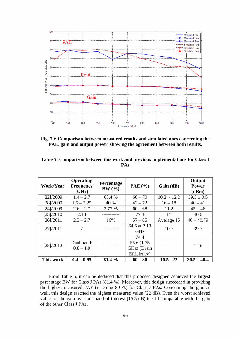
66
Fig. 70: Comparison between measured results and simulated ones concerning the PAE, gain and output power, showing the agreement between both results.
Table 5: Comparison between this work and previous implementations for Class J PAs
Work/Year Operating Frequency
(GHz)
Percentage BW (%) PAE (%) Gain (dB)
Output Power (dBm)
[22]/2009 1.4 – 2.7 63.4 % 60 – 70 10.2 - 12.2 39.5 ± 0.5 [28]/2009 1.5 – 2.25 40 % 42 – 72 16 – 18 40 – 41 [24]/2009 2.6 – 2.7 3.77 % 60 – 68 11.2 45 – 46 [23]/2010 2.14 ----------- 77.3 17 40.6 [26]/2011 2.3 – 2.7 16% 57 – 65 Average 15 40 – 40.79
[27]/2011 2 ----------- 64.5 at 2.13 GHz 10.7 39.7
[25]/2012 Dual band: 0.8 – 1.9 -----------
74.4 56.6 (1.75
GHz) (Drain Efficiency)
----------- ≈ 46
This work 0.4 – 0.95 81.4 % 60 – 80 16.5 - 22 36.5 – 40.4 From Table 5, it can be deduced that this proposed designed achieved the largest
percentage BW for Class J PAs (81.4 %). Moreover, this design succeeded in providing the highest measured PAE (reaching 80 %) for Class J PAs. Concerning the gain as well, this design reached the highest measured value (22 dB). Even the worst achieved value for the gain over our band of interest (16.5 dB) is still comparable with the gain of the other Class J PAs.
67
Chapter 6 : Conclusion and Future Work
In this chapter, conclusions concerning the proposed PA design are deduced based on the measurements and results obtained from Chapter 5. Future work for improving the PA performance is also suggested.
A methodology that is applicable for the design of the main four functional blocks for any Class J PA was discussed in details in Chapter 4. In this suggested methodology, a clear description for the compromises that would be encountered in the design process was given. It emphasized as well on the parameters that govern such compromises to be able to take the appropriate decisions according to the priorities of each design.
Following such methodology, and acting as an illustrative example for verifying these proposed steps, the design of the TV-band CR system’s PA was introduced. Simulations results obtained from accurate modeling for the complete PA circuit were presented, and helped in verifying the expected performance of the Class J mode that was previously described in the literature review. Circuit implementation followed and a comprehensive measurement setup was used to compute the measurement results, which were then compared with the ones obtained from the simulation and proved excellent agreement. The final results were then compared with the previously implemented Class J PAs.
This fabricated PA, to the author’s knowledge, is the first implementation for a Class J PA in this frequency band. From the comparison with the previously realized Class J PAs, it can be deduced that this design achieved the largest percentage BW obtained using Class J PAs (81.4 %). Moreover, this design succeeded in providing the highest measured PAE (reaching 80 %) for Class J PAs. Such results and deductions were finally reported in a scientific paper that was accepted in the PIERS (Progress in Electromagnetic Research Symposium) conference, Stockholm 2013 [34].
As for the suggested future work, the first step should be trying to upgrade the measurement setup with new equipment that would enable the observation of the linearity performance of the circuit, so as to be able to compare it with the simulation results. Consequently, a linearization technique, such as the pre-distortion, can be adopted in order to enhance the measured linearity, yet without degrading the other performance metrics.
Bearing in mind the requirements and applications for any CR system, it may be useful if the available bandwidth is extended, thus enhancing the capabilities of such system. One way to do this is through the modification of the PA design so as to cover the whole TV band (50 MHz till 1000 GHz). Although the design methodology that was described in Chapter 4 will still be valid, it is expected that the design of the matching networks will be much more complicated for such an ultra-wide band and may require more than a single stage to be achieved.
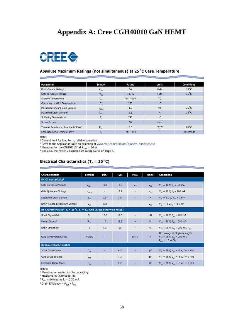
68
Appendix A: Cree CGH40010 GaN HEMT
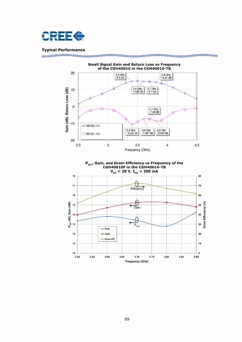
69
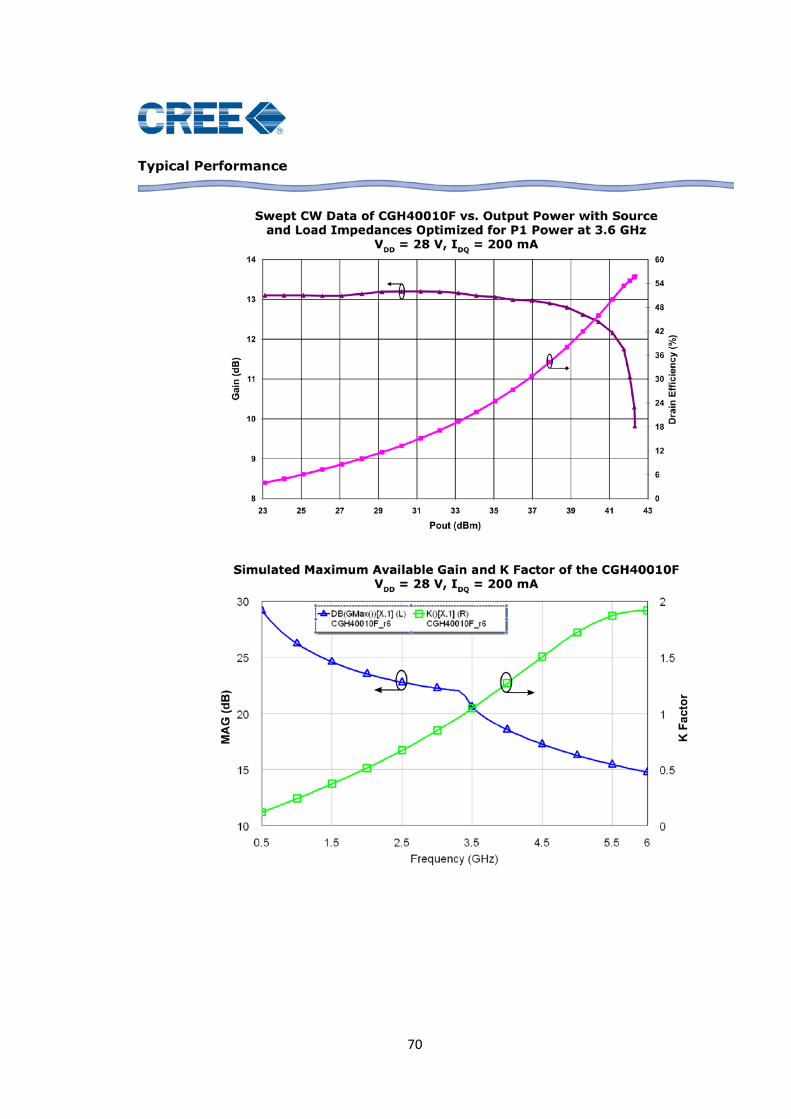
70

71

72
Appendix B: Stability Tests
The stability of an amplifier or its resistance to oscillate is a very important consideration in a design and can be determined from the S- parameters, the matching networks and the terminations. In a two-port network as shown in Fig. 71, oscillations are possible when |Γin| > 1 and |Γout| > 1
Fig. 71: Stability in a 2 ports network
There are several possible tests for the stability; the most commonly used are the μ test and the K- ∆ test. In the K – ∆ stability test, we have
𝐾 =1 − |𝑆11|2 − |𝑆22|2 + |∆|2
2|𝑆12𝑆21|
where ∆= 𝑆11𝑆22 − 𝑆12𝑆21
𝐵 = 1 + |𝑆11|2 − |𝑆22|2 + |∆|2
and the necessary and sufficient conditions for unconditional stability is that
𝐾 > 1 , 𝐵 > 0 In the μ test, where
µ =1 − |𝑆11|2
|𝑆22 − ∆𝑆11∗ | + |𝑆12𝑆21|
unconditional stability is achieved if µ > 1 .

73
References
1. J. Mitola and Jr. G. Q. Maguire, “Cognitive radio: making software radios more personal,” IEEE Pers. Commun., vol. 6, no. 4, pp. 13-18, Aug. 1999.
2. B. Sayrac, “Introduction to cognitive radio,” in Cognitive Radio and its Application for Next Generation Cellular and Wireless Networks (Lecture Notes in Electrical Engineering), vol. 116, H. Venkataraman and G.M. Muntean, Netherlands: Springer, 2012, pp. 3–26.
3. National Telecommunication Regulatory Authority. [Online]. Available: http://www.tra.gov.eg
4. S. Haykin, "Cognitive radio: brain-empowered wireless communications," IEEE J. Sel. Areas Commun., vol. 23, no. 2, pp. 201-220, Feb. 2005.
5. Federal Communication Commission. [Online]. Available: http://www.fcc.gov/
6. National Telecommunications and Information Administration. [Online]. Available: http://www.ntia.doc.gov/
7. IEEE Standard Definitions and Concepts for Dynamic Spectrum Access: Terminology Relating to Emerging Wireless Networks, System Functionality, and Spectrum Management, IEEE Standard 1900.1, 2008.
8. Wireless Innovation Forum. SDR Forum Version 2 [Online]. Available: http://www.sdrforum .org/
9. Virginia Polytechnic Institute and State University. Wireless @ VT [Online]. Available: http://wireless.vt.edu/research/Cognitive_Radios_Networks/
10. J. Mitola. Cognitive Radio Architecture: The Engineering Foundations of Radio XML. Hoboken, NJ: John Wiley & Sons Inc., 2006.
11. S.C. Cripps. RF Power Amplifiers for Wireless Communications. 2nd ed. Norwood, MA: Artech House, 2006.
12. G. González. Microwave transistor amplifiers: analysis and design. 2nd ed. Upper Saddle River, NJ: Prentice Hall, 1997.
13. K. K. Clarke and D. T. Hess. Communications Circuits: Analysis and Design. Reading, MA: Addison-Wesley Publishing Co., 1971; reprinted Malabar, FL: Krieger, 1994.
14. H. L. Krauss, C. W. Bostian, and F. H. Raab. Solid State Radio Engineering. New York, NY: John Wiley & Sons, 1980.
15. M.K. Kazimierczuk. RF Power Amplifiers. United Kingdom: John Wiley & Sons, 2008.
16. P. Reynaret and M. Steyear. RF Power Amplifiers for Mobile Communications. Dordrecht, Netherlands: Springer, 2006.
17. D. M. Pozar. Microwave Engineering. 3rd ed. Hoboken, NJ: John Wiley & Sons Inc., 2009.

74
18. A. Rajaie, A. Khorshid and A. Darwish, “Recent implementations of Class-E power amplifiers,” 2012 Japan-Egypt Electronics, Communications and Computers (JEC-ECC) Conf., Egypt, 2012, pp.26-30.
19. P. Colantonio, F. Giannini, G. Leuzzi, and E. Limiti, “High efficiency low-voltage power amplifier design by second harmonic manipulation,” Int. J. RF Microw. Comput.-Aided Eng., vol. 10, no. 1, pp.19–32, Jan. 2000.
20. P. Colantonio, F. Giannini, G. Leuzzi, and E. Limiti, “Theoretical facet and experimental results of harmonic tuned PAs,” Int. J. RF Microw. Comput.-Aided Eng., vol. 13, no. 6, pp. 459–472, Nov. 2003.
21. P. Wright, J. Lees, J. Benedikt , P. J. Tasker and S. C. Cripps, “A Methodology for Realizing High Efficiency Class-J in a Linear and Broadband PA,” IEEE Trans. Microw. Theory Tech., vol. 57, no. 12, pp. 3196-3204, Dec. 2009.
22. P. Wright, J. Lees, P. J. Tasker, J. Benedikt, and S. C. Cripps, “An efficient, linear, broadband class-J-mode PA realised using waveform engineering,” in IEEE MTT-S Int. Microw. Symp. Dig., Boston, MA 2009, pp. 653–656.
23. J. Moon, J. Kim and B. Kim, “Investigation of a Class-J Power Amplifier with a Nonlinear 𝐶𝑜𝑢𝑡 for Optimized Operation,” IEEE Trans. Microw. Theory Tech., vol. 58, no. 11, pp. 2800-2811, Nov. 2010.
24. J. Kim, J. Moon, J. Kim, S. Boumaiza and B. Kim, “A novel design method of highly efficient saturated power amplifier based on self-generated harmonic currents,” Microwave Conf. EuMC 2009. European , 2009, pp. 1082-1085.
25. X. Fu, D. T. Bespalko and S. Boumaiza, “Novel dual-band matching network topology and its application for the design of dual-band Class J power amplifiers,” Microwave Symp. Dig. (MTT), 2012 IEEE MTT-S Int., Montreal, QC, Canada, 2012, pp. 1-3.
26. N. Tuffy, A. Zhu and T. J. Brazil, “Class-J RF power amplifier with wideband harmonic suppression,” Microwave Symp. Dig. (MTT), IEEE MTT-S Int., Baltimore, MD, 2011, pp. 1-4.
27. K. Mimis, K. A. Morris and J. P. McGeehan, “A 2GHz GaN Class-J power amplifier for base station applications,” Power Amplifiers for Wireless and Radio Applications (PAWR), IEEE Topical Conf. , 2011, pp. 5-8.
28. T. Zhang, “Wideband Hybrid-Class Power Amplifier for Base Station Applications Using LDMOS with Envelope Tracking System,” M.S. thesis, Dept. Elect. Eng. Math. Comput. Sci., Delft Univ. of Technology, Netherlands, 2009.
29. A. Khorshid, A. Rajaie and A. Darwish, “Delivering maximum power from microwave transistors,” 29th Nat. Radio Science Conf. (NRSC), Egypt, 2012, pp. 53-55.
30. AWR Corporation. MWO Getting Started Guide (9th ed.) [Online]. Available: http://www.awrcorp.com/products/microwave-office
31. Cree Inc. (30 Apr. 2012). Data sheet for CGH40010 [Online]. Available: http://ww.cree.com/ rf/products
32. National telecommunication Institute. [Online]. Available: http://www.nti.sci.eg/
33. AMCOM Communications Inc. Data sheet for AM072239UM-2H. [Online]. Available: http://www.amcomusa.com/

75
34. A. E. Khorshid, A. M. Darwish, I. A. Eshrah, H. A. H. Fahmy and M. El-Hadidy, “Broadband High Efficiency Amplifier For a Cognitive Radio System” Progress In Electromagnetics Research Symp. (PIERS), Sweden, 2013, to be published.

ملخصال
كفاءة عالية من المتطلبات الضرورية فى عملية تصميم يعتبر االحتياج إلى مكبر قدرة ذى العديد من التطبيقات فى الوقت الحالى. ويعتبر تخفيض تكاليف التشغيل و الوصول لقدرات
تصاالت، و األساسية و المستهدفة فى نظم اال عالية فى التعامل مع البيانات من الخصائصيتم فى المرحلة الخاصة بمكبر القدرة فإن المنهجية المتبعة ًا من استهالك القدرةكبير اً ألن جزء
المهدرة و بالتالى تحسين حت ذات أهمية قصوى فى تقليل القدرةفى تصميم مكبر القدرة أصب أداء النظام.
تصاالت أصبحت تخضع لتطورات مذهلة نتيجة لألبحاث المكثفة ونظرا ألن أنظمة و معايير االمن أجل مواجهة المتطلبات المتزايدة التى تفرضها التطبيقات الحديثة، التى تتم فى هذا المجال
فإن ذلك يحتاج بالضرورة إلى تحسين و تطوير األجهزة الحديثة و التى تعتبر لبنات البناء لمثل هرت هذه النظم. وـتعتبر أنظمة الراديو المعرفى واحدة من هذه التطبيقات المتطورة و التى ظ
حتياجات و التطورات.نتيجة لمثل هذه االإال أن بناء أنظمة الراديو المعرفى تتطلب بالضرورة منهجيات و طرق حديثة و مبتكرة فى التصميم، سواء على مستوى النظام نفسه أو األجهزة الخاصة به، وذلك حتى يستطيع المنافسة
ة مما يتطلب ر القدر فى السوق التجارى. و تنعكس هذه المتطلبات أيضا على عملية تصميم مكبوالقدرات االستقرارشتراطات و المتطلبات كالكفاءة العالية و سعة النطاق و تحقيق بعض اال
المخرجة العالية و الخطية الجيدة.يشمل هذا البحث دراسة تحليلية ألنواع مكبرات القدرة التقليدية المتاحة وكذلك األساليب الحديثة
قترحة على مدار السنوات األخيرة، ومن ثم يعرض هذا المتبعة فى تصميم مكبرات القدرة، والمكفاءة عالية كجزء من نظام ) واسع النطاق و ذىJالبحث تصميم مبتكر لمكبر قدرة من النوع (
الراديو المعرفى للعمل فى نطاق ترددات التلفاز، و هو يعد أول تصميم من هذا النوع فى هذا النطاق من الترددات.جيجاهرتز، 1جيجاهرتز و حتى 0.4ميم المقترح فى تغطية التردد من و لقد نجح هذا التص
% و هى أعلى نسبة يتم تحقيقها باستخدام هذا النوع 85.7محققا بذلك نسبة نطاق مئوية تبلغ % على مدار هذا النطاق من الترددات بأكمله.60من مكبرات القدرة، و بكفاءة تتعدى ال

أحمد عيسى فنحى خورشيد :دسـمهن ١٩٨٨ \ ٦ \ ٣ تاريخ الميالد:
مصرى الجنسية: ٢٠١٠ \ ١٠ \ ١ تاريخ التسجيل:
\ \ تاريخ المنح: هندسة االلكترونيات و االتصاالت الكهربية القسم: ماجستير الدرجة:
حسام على حسن فهمى .د.أ المشرفون: .د. إسالم عبد الستار أحمد عشرةأ
على محمد على درويش د. أ.
(الكلية الفنية العسكرية) (الممتحن الخارجي) أحمد عبد النظير أحمد محمد. دأ. الممتحنون: (الممتحن الداخلي) مجدى فكرى محمد رجائى .أ.د (المشرف الرئيسي) حسام على حسن فهمى .أ.د
(عضو) إسالم عبد الستار أحمد عشرةأ.د. (عضو)على محمد على درويش أ.د.
عنوان الرسالة: ألنظمة الراديو المعرفى واسع النطاق و ذو كفاءة عالية (J ) عقدرة من النو مكبر
الكلمات الدالة: سحب. -، الحمل (J ) عالنو ، كفاءة، واسع النطاق، قدرة اتمكبر
:رسالةملخـص اليعتبر اإلحتياج إلى مكبر قدرة ذو كفاءة عالية من المتطلبات الضرورية فى عملية تصميم العديد من
مع التطبيقات فى الوقت الحالى. ويعتبر تخفيض تكاليف التشغيل و الوصول لقدرات عالية فى التعامل البيانات من الخصائص األساسية و المستهدفة فى نظم األتصاالت، و ألن جزء كبير من استهالك القوة يتم فى المرحلة الخاصة بمكبر القدرة فإن المنهجية المتبعة فى تصميم مكبر القدرة أصبحت ذات أهمية قصوى
يشمل هذا البحث دراسة تحليلية ألنواع مكبرات القدرة النظام. فى تقليل القوة المهدرة و بالتالى تحسين أداءالتقليدية المتاحة وكذلك األساليب الحديثة المتبعة فى تصميم مكبرات القدرة، والمقترحة على مدار السنوات
) واسع النطاق و ذو كفاءة Jاألخيرة، ومن ثم يعرض هذا البحث تصميم مبتكر لمكبر قدرة من النوع (نظام الراديو المعرفى للعمل فى نطاق ترددات التلفاز، و هو يعد أول تصميم من هذا النوع عالية كجزء من
جيجاهرتز و ٠.٤و لقد نجح هذا التصميم المقترح فى تغطية التردد من فى هذا النطاق من الترددات.استخدام % و هى أعلى نسبة يتم تحقيقها ب٨٥.٧جيجاهرتز، محققا بذلك نسبة نطاق مئوية تبلغ ١حتى
% على مدار هذا النطاق من الترددات بأكمله.٦٠هذا النوع من مكبرات القدرة، و بكفاءة تتعدى ال
ضع صورتك هنا


ألنظمة الراديو المعرفى واسع النطاق و ذو كفاءة عالية (J ) عقدرة من النو مكبر
اعداد
أحمد عيسى فتحى خورشيد
القاهرة جامعة - الهندسة كلية إلى مقدمة رسالة الماجستير درجة على الحصول متطلبات من كجزء
في هندسة اإللكترونيات و األتصاالت الكهربية
القاهــرة جامعــة - الهندســة كليــة العربيــة مصـر جمهوريـة - الجيـزة
2013


![Selected Topics in Analog Integrated Circuits Lecture 1 ...eece.cu.edu.eg/~maboudina/teachingmat/ELC701Spring... · [REF1] C. C. Enz and E. A. Vittoz, Charge-Based MOS Transistor](https://static.fdocuments.us/doc/165x107/5f6f97f2e5951824ba7a1eee/selected-topics-in-analog-integrated-circuits-lecture-1-eececueduegmaboudinateachingmatelc701spring.jpg)