
Broadband Conformal Phased Array with Optical Beam … Conformal Phased Array with Optical Beam...
17
1 Broadband Conformal Phased Array with Optical Beam Forming for Airborne Satellite Communication H. Schippers, J. Verpoorte, P. Jorna, A. Hulzinga National Aerospace Laboratory NLR Anthony Fokkerweg 2, 1006 BM Amsterdam, the Netherlands [email protected] A. Meijerink, C. G. H. Roeloffzen, L. Zhuang , D. A. I. Marpaung, W. van Etten Telecommunication Engineering group, Faculty of Electrical Engineering University of Twente, P.O.Box 217, 7500 AE, Enschede, the Netherlands [email protected] R. G. Heideman, A. Leinse, A. Borreman, M. Hoekman LioniX bv P.O. Box 456, 7500 AH Enschede, the Netherlands [email protected] M. Wintels Cyner Substrates Savannahweg 60, 3542 AW Utrecht, the Netherlands [email protected] Abstract—For enhanced communication on board an aircraft, novel antenna systems with broadband satellite- based capabilities are required. The technology will enhance airline operations by providing in-flight connectivity for flight crew information and will bring live TV and high- speed Internet connectivity to passengers. The installation of such systems on board an aircraft requires for aerodynamic reasons the development a very low-profile aircraft antenna, which can point to satellites anywhere in the upper hemisphere. To this end, phased array antennas which are conformal to the aircraft fuselage are attractive. In this paper, two key aspects of conformal phased array antenna arrays are addressed: the development of a broadband Ku-band antenna and an optical beam forming network for tracking satellites. The antenna elements of the conformal array are stacked patch antennas with dual linear polarization which have sufficient bandwidth. For tracking an optical circuit is proposed that consists of a cascade of optical ring resonators. 12 TABLE OF CONTENTS 1. INTRODUCTION...................................................... 1 2. SYSTEM ASPECTS .................................................. 3 3. DEVELOPMENT OF KU-BAND ANTENNA ............... 4 4. DEVELOPMENT OF OPTICAL BEAMFORMER ........ 5 5. EXPERIMENTAL RESULTS ................................... 10 6. DEVELOPMENT OF DEMONSTRATOR .................. 11 7. CONCLUSIONS ..................................................... 11 ACKNOWLEDGMENT ............................................... 12 REFERENCES ........................................................... 13 BIOGRAPHIES .......................................................... 15 1 1 1-4244-1488-1/08/$25.00 ©2008 IEEE 2 IEEEAC paper #1231, Version 5, Updated January 19, 2008 1. INTRODUCTION For enhanced communication on board of aircraft novel antenna systems with broadband satellite-based capabilities are required. The technology must bring live weather reports to pilots, as well as live TV and high-speed Internet connectivity to passengers. Satellite communication services can be provided by Low Earth Orbiting (LEO) systems and Geostationary (GEO) systems. Altitudes of LEO satellites range between 700 and 1500 km over the Earth. The round-trip delay is only a few milliseconds, and free space propagation losses are low enough to make handheld terminals easily achievable. Well-known LEO systems are Iridium and Globalstar. The satellite orbits are optimised to provide highest link availability in the area between 70 ± degrees latitude on earth. Each satellite pass, as viewed from a user location on earth, typically lasts about 10-15 minutes. For geostationary communication systems much fewer satellites are required to provide coverage on earth. For instance, Inmarsat uses only two I4 satellites to provide coverage to around 85 per cent of the world's landmass and 98 per cent of the world's population. Today there are more than 300 operational geostationary satellites. These satellites are fixed at an altitude of approximately 36.000 km at the equator. These satellites are being using for television broadcasting, communications and weather forecasting. In general, receiving and transmitting antennas on the earth do not need to track such a satellite. These antennas can be fixed in place and are much less expensive than tracking antennas. An increasing number of Ku-band TV geostationary satellites is approaching end of life. Most satellites are still in a good technical state, but the level of propulsion fuel
Transcript of Broadband Conformal Phased Array with Optical Beam … Conformal Phased Array with Optical Beam...
1
Broadband Conformal Phased Array with Optical Beam Forming for Airborne Satellite Communication
H. Schippers, J. Verpoorte, P. Jorna, A. Hulzinga
National Aerospace Laboratory NLR Anthony Fokkerweg 2, 1006 BM Amsterdam, the Netherlands
[email protected] A. Meijerink, C. G. H. Roeloffzen, L. Zhuang , D. A. I. Marpaung, W. van Etten
Telecommunication Engineering group, Faculty of Electrical Engineering University of Twente, P.O.Box 217, 7500 AE, Enschede, the Netherlands
[email protected] R. G. Heideman, A. Leinse, A. Borreman, M. Hoekman
LioniX bv P.O. Box 456, 7500 AH Enschede, the Netherlands
[email protected] M. Wintels
Cyner Substrates Savannahweg 60, 3542 AW Utrecht, the Netherlands
[email protected] Abstract—For enhanced communication on board an aircraft, novel antenna systems with broadband satellite-based capabilities are required. The technology will enhance airline operations by providing in-flight connectivity for flight crew information and will bring live TV and high-speed Internet connectivity to passengers. The installation of such systems on board an aircraft requires for aerodynamic reasons the development a very low-profile aircraft antenna, which can point to satellites anywhere in the upper hemisphere. To this end, phased array antennas which are conformal to the aircraft fuselage are attractive. In this paper, two key aspects of conformal phased array antenna arrays are addressed: the development of a broadband Ku-band antenna and an optical beam forming network for tracking satellites. The antenna elements of the conformal array are stacked patch antennas with dual linear polarization which have sufficient bandwidth. For tracking an optical circuit is proposed that consists of a cascade of optical ring resonators.12
TABLE OF CONTENTS
1. INTRODUCTION......................................................1 2. SYSTEM ASPECTS ..................................................3 3. DEVELOPMENT OF KU-BAND ANTENNA ...............4 4. DEVELOPMENT OF OPTICAL BEAMFORMER........5 5. EXPERIMENTAL RESULTS ...................................10 6. DEVELOPMENT OF DEMONSTRATOR..................11 7. CONCLUSIONS .....................................................11 ACKNOWLEDGMENT ...............................................12 REFERENCES ...........................................................13 BIOGRAPHIES ..........................................................15
1 1 1-4244-1488-1/08/$25.00 ©2008 IEEE 2 IEEEAC paper #1231, Version 5, Updated January 19, 2008
1. INTRODUCTION
For enhanced communication on board of aircraft novel antenna systems with broadband satellite-based capabilities are required. The technology must bring live weather reports to pilots, as well as live TV and high-speed Internet connectivity to passengers. Satellite communication services can be provided by Low Earth Orbiting (LEO) systems and Geostationary (GEO) systems. Altitudes of LEO satellites range between 700 and 1500 km over the Earth. The round-trip delay is only a few milliseconds, and free space propagation losses are low enough to make handheld terminals easily achievable. Well-known LEO systems are Iridium and Globalstar. The satellite orbits are optimised to provide highest link availability in the area between 70± degrees latitude on earth. Each satellite pass, as viewed from a user location on earth, typically lasts about 10-15 minutes. For geostationary communication systems much fewer satellites are required to provide coverage on earth. For instance, Inmarsat uses only two I4 satellites to provide coverage to around 85 per cent of the world's landmass and 98 per cent of the world's population. Today there are more than 300 operational geostationary satellites. These satellites are fixed at an altitude of approximately 36.000 km at the equator. These satellites are being using for television broadcasting, communications and weather forecasting. In general, receiving and transmitting antennas on the earth do not need to track such a satellite. These antennas can be fixed in place and are much less expensive than tracking antennas.
An increasing number of Ku-band TV geostationary satellites is approaching end of life. Most satellites are still in a good technical state, but the level of propulsion fuel

2
does not allow full orbital control. With a reduced amount of fuel the east-west position of these satellites can be controlled, while the inclination angle will slightly increase every year. Then, these are not very useful anymore for general TV broadcasting, since millions of users are equipped with fixed pointing antennas. Instead tracking antennas should be needed, but they are more expensive. However, when the mobile terminal for satellite communication is moving (for instance when applied on a flying aircraft) a tracking antenna is required in all circumstances. Many studies are going on worldwide to employ these Ku-band geostationary satellites for communication with mobile terminals on cars, trains, ships and aircraft. For a short period broadband internet was available on aircraft via Connexion by Boeing (CBB) services. Lufthansa installed the CBB system on some of their long-haul aircraft. In 2006 the CBB services ended, because the consumer market for this service had not materialized as was expected. In August 2007 the US government awarded a contract to Boeing for providing Boeing Broadband Satcom Network (BBSN) services to the U.S. Air Force Air Mobility Command. BBSN has to provide high-speed Internet communications and direct broadcast satellite TV service as a cost effective solution for the U.S. government's aircraft and airborne customers. Supported aircraft include C-32s, C-40s, E-4s as well as the full spectrum of VIP and special air mission aircraft.
Ku-band terminals on board moving platforms require antennas with high gain in which the main beam can continuously be steered to geostationary satellites. To this end the following types of antenna systems can be identified:
- Mechanically steered reflector antennas (see Figure 1).
- Mechanically steered array antennas (beam of array is fixed, but mechanically steered).
- Electronically steered phased array antennas.
- Hybrid steered antennas; such antennas are normally mechanically steered in one direction (e.g. azimuth), in electronically in the other direction (e.g. elevation).
Mechanically steered reflector and array antennas require a large radome for reasons of protection. Such a radome increases the aerodynamic drag and requires additional cuts and stiffeners in the fuselage structure. On the other hand, conformal electronically steered phased array antennas offer several advantages over mechanically steered reflector antennas, and designers should take advantage of the improvements these conformal antennas offer. The conformal antennas should have similar antenna characteristics with high scan capabilities at high latitudes. In addition the antenna should be able to withstand severe
environmental conditions such as temperature, pressure and vibration.
Figure 1 Mechanically steered reflector antenna
Figure 2 Conformal phased array antenna
In the Netherlands, a consortium (consisting of University of Twente, Lionix BV, National Aerospace Laboratory NLR and Cyner Substrates) is developing technology for such conformal airborne antennas. This technology development (carried out in the national FlySmart project) includes two key topics: a broadband conformal Ku-band antenna and a broadband optical beam forming network. The objective of this paper is to present research results of these two key topics.
The antenna front-end consists of a broadband conformal phased array antenna (bandwidth ≥ 2GHz) operating in Ku-band. The antenna elements are stacked patch antennas with dual linear polarization. First results indicate sufficient bandwidth in input impedance and radiation pattern. Special attention is paid to the manufacturability of the antenna by selecting specific materials and appropriate fabrication techniques.
Once the global design of the conformal phased array has been established, further research concerns the verification of its beam steering capabilities. For instance, is it possible to find an optimum set of element excitations for the antenna elements of the array to best satisfy the radiation pattern demands in some well-defined sense and to steer the beam in the direction of the geostationary satellites? The National Aerospace Laboratory NLR has developed an
3
adapted least squares pattern synthesis that yields an efficient tapering for conformal phased arrays (see [1]). This synthesis method is applied to determine the excitations of directive pencil beams of a circularly shaped phased array in Ku-band on a singly curved structure, and to investigate the radiation patterns of beams of conformal phased arrays on top of the fuselage when the aircraft is flying at relatively high latitudes (for instance 70 degrees north of the equator).
For the steering of the beam of the conformal phased array a squint-free, continuously tunable mechanism is proposed that is based on a fully integrated optical beam forming network (OBFN) using cascades of optical ring resonators (ORRs) as tunable delay elements. A narrowband continuously tunable optical true time delay (TTD) device can be realized as a recirculating waveguide coupled to a straight waveguide. This straight waveguide can behave as an all-pass filter with a periodic, bell-shaped tunable group delay response. The maximum group delay occurs at a tunable resonance frequency. A larger delay-bandwidth product can be achieved by cascading multiple ORR sections. A complete OBFN can be obtained by grouping several delays and combining elements in one optical circuit. Such an OBFN can be realized on a single-chip. Electrical/Optical (E/O) and Optical Electrical (O/E) conversion are realised by means of filter based single-sideband modulation (suppressing the carrier) and balanced coherent optical detection.
2. SYSTEM ASPECTS
In the ITU Radio Regulations [2] portions of the Ku-band are allocated to aeronautical services:
- AES receive band 1: 10.70 – 11.70 GHz (primary allocation to fixed satellite service)
- AES receive band 2: 12.50 – 12.75 GHz (primary allocation to fixed satellite service)
- AES transmit band: 14.00 – 14.50 GHz (secondary allocation to mobile satellite service)
The Aeronautical Earth Stations (AES) have to comply with ITU-R RECOMMENDATION M.1643 [3] and with ETSI EN 302 186 [4], a harmonised European Norm for satellite mobile Aircraft Earth Stations (AESs) operating in the 11/12/14 GHz frequency band.
In addition, reception of commercial satellite broadcasts is of interest:
- Satellite TV: 11.70 – 12.50 GHz (primary allocation to broadcast satellite service)
In the Dutch FlySmart project, only the receive antenna system will be developed. The objective is to develop a conformal phased array antenna having an instantaneous bandwidth of 2 GHz, covering the whole frequency range of 10.7 to 12.75 GHz.
Satellites operating in this band are geostationary satellites spaced 2o apart in the United States and 3o in Europe. In order to be able to receive these satellites also at high latitudes (e.g. during inter-continental flights) the antenna system should have sufficient performance at low elevation angles.
Therefore the antenna system is required to have a small beamwidth (to discriminate between the satellite signals) and a high gain (>30 dB) also at low elevation angles. Since gain of the antenna is related to the effective aperture of the antenna in the direction of the satellites, a conformal antenna also covering side parts of the fuselage could be an advantage.
The phased array antenna shall maintain the proper (linear) polarization during all attitudes and at all positions of the aircraft (also at high latitudes).
An antenna to be used on aircraft has to be able to operate in severe environmental conditions concerning temperature, pressure, vibration and humidity. The environmental requirements for civil airborne equipment are given in RTCA DO-160 or EUROCAE ED-14 [5].
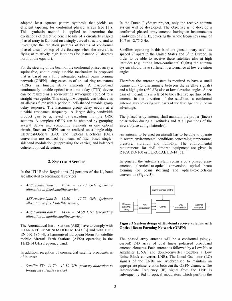
In general, the antenna system consists of a phased array antenna, electrical-to-optical conversion, optical beam forming (or beam steering) and optical-to-electrical conversion (Figure 3).
Figure 3 System design of Ku-band receive antenna with Optical Beam Forming Network (OBFN)
The phased array antenna will be a conformal (singly-curved) 2-D array of dual linear polarised broadband antenna elements. Each antenna is followed by a Low Noise Amplifier (LNA) and down-converter (together a Low Noise Block converter, LNB). The Local Oscillator (LO) signals of the LNBs are synchronised to maintain an appropriate phase relation between the OBFN channels. The Intermediate Frequency (IF) signal from the LNB is subsequently fed to optical modulators which perform the
4
electrical-to-optical conversion. In the Optical Beamforming Network (OBFN) each individual signal is attenuated and delayed in order to shape and direct the antenna beam. The sum of all signals is converted back from the optical to the electrical domain.
The tracking algorithm will use the aircrafts position and attitude to determine the appropriate polarization and azimuth and elevation of the antenna beam.
To reach the objective of a 2 GHz bandwidth, both the antenna front-end and the beamforming network should have broadband characteristics. Therefore, the antenna front-end consists of an array of stacked patch antennas. The beamforming network consists of an optical network with True Time Delays (TTD) which have inherently large bandwidth. To have a 2o beamwidth and high gain antenna (approx. 36 dB), a large array antenna is needed. The current design is based on an array of 40 by 40 antenna elements (1600 in total).
3. DEVELOPMENT OF KU-BAND ANTENNA
The objective is to develop a very low-profile aircraft antenna, which can point to geostationary satellites anywhere in the upper hemisphere. Traditionally, reflector-based solutions have been proposed which are unattractive to airlines since they create significant drag and push up fuel costs. Instead conformal phased array antennas of which the main beam can electronically be steered are recommended. In general an array antenna consists of a multiple of active antenna elements coupled to a common source to produce a directive radiation pattern. The antenna element could be any type, but should have an omni-directional radiation pattern. Since the aircraft antenna should have a low profile most suitable antenna elements are microstrip patches, which are fed by apertures in a ground plane. The main disadvantage of these microstrip patch antennas is their limited bandwidth which is in the order of a few percent for a typical patch radiator. This property makes the classical patch antennas less attractive for broadband satellite communication. In order to increase the bandwidth, stacked patches have been advocated in literature. In the stacked patch configuration a parasitic element is placed above a lower patch, separated by foam or other space filler. In this manner, bandwidths on the order of 30–35% can be achieved [6]. In this section we present the design of stacked patch Ku-band antenna element and we discuss the preliminary design of a conformal array of stacked Ku-band antenna elements.
Design of single Ku-band antenna element
A common approach for increasing the bandwidth is to add parasitic elements to the antenna structure (e.g. a stacked patch). This reduces the impedance variation of the antenna with the frequency, thus enhancing bandwidth performance.
Various arrangements of stacked structures have been investigated in [7] and [8].In practice, it is difficult to optimise the bandwidth of these structures due to their sensitivity with respect to many physical parameters (patch sizes, substrate thicknesses, and feed-point position). Research has focused on the choice of the materials for the dielectric layers in the stacked configuration. Thick laminates of low-dielectric constant provide the largest bandwidth and surface wave efficiency (see [8]).
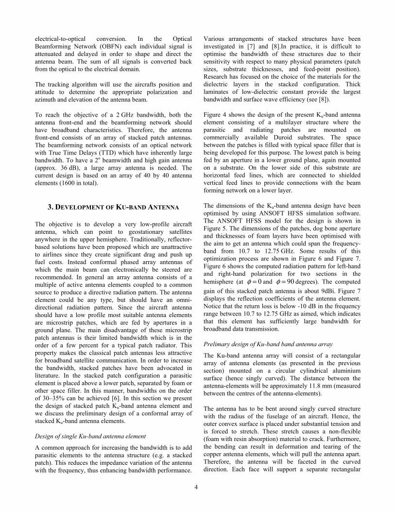
Figure 4 shows the design of the present Ku-band antenna element consisting of a multilayer structure where the parasitic and radiating patches are mounted on commercially available Duroid substrates. The space between the patches is filled with typical space filler that is being developed for this purpose. The lowest patch is being fed by an aperture in a lower ground plane, again mounted on a substrate. On the lower side of this substrate are horizontal feed lines, which are connected to shielded vertical feed lines to provide connections with the beam forming network on a lower layer.
The dimensions of the Ku-band antenna design have been optimised by using ANSOFT HFSS simulation software. The ANSOFT HFSS model for the design is shown in Figure 5. The dimensions of the patches, dog bone aperture and thicknesses of foam layers have been optimised with the aim to get an antenna which could span the frequency-band from 10.7 to 12.75 GHz. Some results of this optimization process are shown in Figure 6 and Figure 7. Figure 6 shows the computed radiation pattern for left-hand and right-hand polarization for two sections in the hemisphere (at 0φ = and 90φ = degrees). The computed gain of this stacked patch antenna is about 9dBi. Figure 7 displays the reflection coefficients of the antenna element. Notice that the return loss is below -10 dB in the frequency range between 10.7 to 12.75 GHz as aimed, which indicates that this element has sufficiently large bandwidth for broadband data transmission.
Prelimary design of Ku-band band antenna array
The Ku-band antenna array will consist of a rectangular array of antenna elements (as presented in the previous section) mounted on a circular cylindrical aluminium surface (hence singly curved). The distance between the antenna-elements will be approximately 11.8 mm (measured between the centres of the antenna-elements).
The antenna has to be bent around singly curved structure with the radius of the fuselage of an aircraft. Hence, the outer convex surface is placed under substantial tension and is forced to stretch. These stretch causes a non-flexible (foam with resin absorption) material to crack. Furthermore, the bending can result in deformation and tearing of the copper antenna elements, which will pull the antenna apart. Therefore, the antenna will be faceted in the curved direction. Each face will support a separate rectangular

5
array of Ku-band antenna elements (with only a few elements in azimuth direction). On the upper side of the antenna structure small notches will be made to provide the curvature. Preliminary vibration tests using a sample structure were promising.
Two planar samples with Ku-band arrays have been manufactured. The first sample consisted of an array of 8x1 antenna-elements, the second sample had 8x8 elements. Some results of coupling measurements and computations are presented in section 5.
Substrate
Foam replacement
Substrate
Substrate
Substrate
Patch
Feed
Ground
Dogbone
Patch
Feedline routed on special feedline layer(s)
Shielded vertical feedline
Substrate
Foam replacement
Substrate
Substrate
Substrate
Substrate
Foam replacement
Substrate
Substrate
Substrate
Substrate
Foam replacement
Substrate
Substrate
Substrate
Patch
Feed
Ground
Dogbone
Patch
Feedline routed on special feedline layer(s)
Shielded vertical feedline
Figure 4 Design of stacked Ku-band antenna element
Figure 5 ANSOFT HFSS model for stacked Ku-band patch antenna
Figure 6 Radiation patterns for stacked Ku-band patch antenna (linear co-and cross polar components)
Figure 7 Reflection coefficients of stacked Ku-band patch antenna
4. DEVELOPMENT OF OPTICAL BEAMFORMER
Implementing the beamformer in the optical domain shares many common advantages with other RF photonic signal processing techniques [10],[11], such as compactness and light weight (particularly when integrated on a chip), low loss, frequency independence, large instantaneous bandwidth, and inherent immunity to electromagnetic interference. Most previously proposed optical beamformer systems are either based on optical phase shifters [12] or switchable delay matrices [13]. However, phase shifters do not provide true time delay (TTD), and therefore result in a frequency-dependent beam angle and shape (beam squint). Switchable delay matrices are not continuously tunable: they show a trade-off between beam angle resolution and complexity. An alternative that offers both continuous tunability and TTD is based on chirped fibre gratings (CFGs) [14]–[16], but this technique has the disadvantage of requiring bulky optical components and an (expensive) tunable laser.
In this section a squint-free, continuously tunable OBF mechanism for a phased array receiver system is proposed

6
that does not require a tunable laser. It is based on a fully integrated optical beam forming network (OBFN) using cascades of optical ring resonators (ORRs) as tunable delay elements. A dedicated system architecture is proposed that relaxes the requirements on optical modulators and detectors, and on the OBFN itself. It has a potential for full beamformer integration.
This section is organized as follows. In the next subsection, the theoretical principles of ORR-based delay elements will be summarized. After that it will be explained how these delay elements should be grouped into an OBFN. In the third subsection the complete system architecture around this OBFN will be described, with particular focuss on how the electro-optical and opto-electrical conversions should be performed. The section will end with a description of the fabrication technology for the optical chips.
Ring Resonator-Based Delays
In the waveguide realization an ORR-based delay element consists of a straight waveguide and a recirculating waveguide coupled parallel to it. This is illustrated in the inset of Figure 8, where three of such ORR sections are cascaded. An ideal lossless ORR section acts as an optical all-pass filter, which is characterized by a unity magnitude response. It has a periodic group delay response, which represents the effective time delay to the RF signal that is modulated on the optical carrier signal. A mathematical expression for this group delay response is given by [17]–[20]
,) π2cos(122
)(g φκκκτ
+−−−=
TfTf (1)
in which T is the round-trip time of the light in the ring, or in other words, 1/T is the free spectral range (FSR) of the ORR. κ is the power coupling coefficient of the coupler, and φ is the additional round-trip phase shift of the ring. Within one FSR of the group delay response (shown by the dashed lines in Figure 8) a delay peak is centered at the resonance frequency, which is intended to be used to delay the RF signal. The peak value of the delay and the resonance frequency are determined by the (tunable) parameters κ and φ, respectively, which facilitates the continuous tunability of the ORR-based delay element. However, the peak value of the delay is more or less inversely proportional to the peak width. This is because the area underneath the delay curve in one FSR is equal to 1/(2π) times the phase transition within one FSR. Since this phase transition is constant (2π), the area under the group delay response in one FSR is also constant (unity). Hence, when the peak delay value of the ORR is increased, the bandwidth decreases, revealing an inherent trade-off of the ORR-based delay [17]–[21].
f1 f2 f30
→ f
→ g
roup
del
ay
κ1 κ2 κ3
φ1 φ2 φ3
in outT T T
Figure 8 – Theoretical group delay response of three cascaded ORR sections. The dashed lines represent the group delay responses of the individual sections. (Inset: cascade of three ORRs with round-trip delay T, additional round-trip phase-shifts φi and power coupling coefficients κi.)
For a broadband RF signal a single ORR may not provide enough delay bandwidth. In this case multi-ring delay elements can be used instead. A multi-ring delay element is built by cascading multiple ORR sections, as shown in the inset of Figure 8. Each ring can be tuned independently, and the individual group delay responses superpose to form the eventual group delay response of the multi-ring delay element. When the rings are properly tuned, to different resonance frequencies, a group delay response with a flattened delay band can be achieved, as shown in Figure 8. It can be seen that delay ripples appear in the flattened delay band. This delay ripple may cause signal distortion and is inevitable, but can be reduced to an acceptable level by squeezing the resonance frequencies closer to each other or by adding more rings in the cascade. The second approach, however, increases the tuning complexity of the delay element. Hence, multi-ring delay elements show an inherent trade-off between peak delay, bandwidth, delay ripple, and number of rings [17],[19]–[21].
In [21] we have presented group delay measurements on a three-ring optical delay device —realized in CMOS-compatible optical waveguide technology [22]–[24]— showing good agreement with this theory.
Optical Beam Forming Network
When the optical delay elements are combined with tunable signal processing circuitry (power splitters or combiners), an OBFN is formed. Integrating such an OBFN into one single optical chip has many advantages compared to connecting separate optical devices, such as compact size, light weight, low loss, and reduced costs. Moreover, integration on chip facilitates coherent optical combining, so that only one laser and one detector are required in a complete phased array receiver system, as we will see in the next subsection.
Figure 9 shows an ORR-based 1×8 OBFN for a transmitter phased array, based on a binary tree topology. It consists of

7
three stages and has eight outputs. In this case twelve ORRs and seven tunable power splitters are involved. The OBFN is arranged in such a way that an increasing number of ORRs is cascaded for Outputs 1 to 8, to satisfy the delay requirement for beam forming in a linear phased array. Compared to the parallel topology, which has independent cascades of ORRs for each output, the binary tree-based OBFN is more efficient with respect to the required number of rings, and therefore has a reduced tuning complexity. Moreover, the binary tree-based OBFN is easy to extend: more outputs can be obtained by simply adding more stages.
The first single-chip realization of an ORR-based OBFN, based on a 1×4 binary tree topology, was presented in [25], and later extended to a 1×8 OBFN [26],[27].
Optical Beamformer System Architecture
When an OBFN is applied in a phased array receiver system, the individual antenna element signals first have to be converted from the electrical to the optical domain. The optical signals are then re-aligned and combined by the OBFN, resulting in one output signal that has to be converted back to the electrical domain.
In order to minimize the loss, the combining of the optical signals in the OBFN should preferably be done coherently, which requires the use of a common laser. The output light of the laser should first be split, and then be modulated by the antenna element signals, using external modulators. The most straightforward way of doing so is to apply optical double-sideband (DSB) modulation, for example using Mach-Zehnder modulators (MZMs). The output signal of the OBFN can then be converted to the electrical domain by direct optical detection, using a photodiode. This is illustrated in Figure 10.
A drawback of this approach is the large bandwidth of the modulated optical signal [28]. Its spectrum consists of the optical carrier and —depending on the modulation depth— at least two sidebands. With satellite TV operating in the 10.7–12.75 GHz band, it follows that the optical bandwidth is at least 25.5 GHz. In order to avoid signal distortion in the OBFN, the optical delay elements in the OBFN should provide flat group delay response in the entire frequency range of the modulated optical signal. The large bandwidth of this flat group delay response has two disadvantages [28]:
1. As mentioned earlier, the ORR-based delay elements follow a trade-off between maximum delay, optical bandwidth, delay ripple, and number of ORR sections. With DSB modulation, the product of maximum delay (in the order of nanoseconds) and bandwidth (25.5 GHz) would be such that it can be proven [20] that at least several tens up to several hundreds of rings are required for realizing such tuning range over such a large bandwidth with reasonable group delay ripple. This would result in a very complex OBFN, particularly because all these rings need to be separately tunable;
2. Moreover, a large optical bandwidth requires a large FSR and, hence, a small round-trip time T. Assuming a waveguide group index in the order of 1.8 (see the next subsection), it can be verified that an FSR in the order 25.5 GHz would correspond to a ring circumference of 6.5 mm. In the next subsection it will become clear that this requires the race track-shaped rings to have either relatively small bending radius (resulting in excessive bending losses) or short tuning elements (resulting in inefficient tuning).
As a result, alternative solutions are needed to reduce the bandwidth of the modulated optical signal. A straightforward option would be to apply frequency down conversion to an intermediate frequency (IF) range prior to electro-optical conversion. This has the additional
MZM
I tout( )
MZM
OBFN
LNA
AE
LNA
AE
Figure 10 – Optical beamformer architecture using DSB modulation and direct detection (AE=antenna element, LNA=low-noise amplifier, MZM=Mach-Zehnder modulator, OBFN=optical beam forming network)
κ5 κ6 κ16
φ5 φ6
5 6κ7
φ7
out 27
κ8
φ8
8
κ15
out 1
out 4
out 3κ14
κ9 κ10 κ19
φ9 φ10
9 10κ11
φ11
out 611
κ12
φ12
12
κ18
out 5
out 8
out 7κ17κ3 κ4
φ3 φ4
3 4
κ1 κ2
φ1 φ2
1 2
in
κ13
stage 1 stage 2 stage 3
Figure 9 – Binary tree-based 1×8 optical beam forming network for a phased array transmitter system, consisting of twelve ORRs and seven tunable splitters.
8
advantage that slower (and hence less expensive) optical modulators can be used. However, it has the disadvantage that the local oscillators (LOs) in the downconverters would then need to have tunable phase differences (corresponding to the delays in the OBFN) in order to prevent IF phase offsets, and, moreover, that a relative IF bandwidth in excess of one octave would result in second order intermodulation distortion (IMD-2), which decreases the dynamic range of the receiver. This is further explained in [28].
An alternative approach is to use optical single-sideband (SSB) instead of DSB modulation, reducing the optical bandwidth by half. This can be even further reduced by also suppressing the carrier (SSB-SC modulation), resulting in an optical bandwidth that equals the bandwidth of the modulating (RF) signal [28],[29]. The opto-electrical conversion after the OBFN must then be done by means of coherent optical detection. This can be implemented by routing the unmodulated optical carrier signal around the OBFN, combine it with the OBFN output signal by means of a 2×2 directional coupler, and subtract the output powers of this coupler by means of a balanced detector [28],[29]. This is illustrated in Figure 11.
Advantages of this optical modulation/detection scheme are:
• The optical bandwidth is significantly reduced, thereby reducing the complexity of the OBFN (number of rings), and bringing the bending loss and tuning efficiency in each ring to an acceptable level;
• The balanced detector cancels most of the laser’s relative intensity noise (RIN), thereby significantly increasing the dynamic range of the system [30];
• In case down conversion is performed prior to optical modulation, IF phase offsets can now be corrected by simple optical phase shifts in the OBFN (which are required anyway for coherent combining), and IMD-2 is canceled by the balanced detector [28].
Optical SSB-SC modulation can be implemented in various ways [28], but the simplest way for this particular application is to use DSB modulators followed by optical sideband filters (OSBFs). DSB modulation can be performed by MZMs, which can be biased in such a way that the carrier is inherently suppressed (DSB-SC modulation) [31]. The OSBF is then only required to suppress one of the sidebands. Since the OBFN and OSBF are both linear devices, their order can be reversed, so that only one common OSBF is required, as illustrated in Figure 11.
A logical design choice for the OSBF is to use a filter structure based on the same building blocks as the OBFN (couplers and ORRs). The OSBF can then be realized in the same technology as the OBFN (see the next subsection) and, hence, be integrated on the same chip. We chose to use an unbalanced Mach-Zehnder interferometer with an ORR in the shortest branch, as shown in Figure 12. The circumference of this ORR is twice the path length difference of the MZI. The advantage of such a filter is that it has flattened pass bands and stop bands that can be made relatively wide, with steep transitions in between [29],[32].
Design and Realization of the Optical Chips
As mentioned before, the OSBF can be realized in the same technology as the OBFN, which reduces the fabrication complexity. Using the same technology for different components is a large advantage in VLSI integration.
An important parameter in the realization of the optical chips is the loss induced by the waveguide structures. A very promising technology that can meet the high requirements for the optical chip fabrication is the TriPleX technology of LioniX [22], [24], [33], [34]. This technology consists of a multi-layer stack of LPCVD silicon oxide and nitride. Since all composing materials are end products during the deposition, the material properties are very stable and reproducible and the device properties are therefore only determined by the geometry of the device. The basic steps of the fabrication of the TriPleX waveguides are shown in Figure 13.
With this fabrication technology waveguides with different properties can be fabricated. The difference between the different waveguides is the etch depth in the nitride and the local removal of the Si3N4. In Figure 14 an example of two
MZM
MZM
OSBFOBFN
LNB
AE
LNB
AE
I tout( )
Figure 11 – Optical beamformer architecture using filter-based SSB-SC modulation and balanced coherent detection (AE=antenna element, LNB=low-noise block, MZM=Mach-Zehnder modulator, OBFN=optical beam forming network, OSBF=optical sideband filter)
2Tκ1
T
κ2
κ3
φ2
φ1
Figure 12 – Optical sideband filter (OSBF) consisting of a Mach-Zehnder interferometer (MZI) and an optical ring resonator (ORR)

9
types is shown. The left waveguide is highly polarization-dependent and has a relatively high effective index (~1.65). The waveguide on the right has a slightly lower effective index (~1.5-1.6), but can be fabricated with lower polarization dependency.
Figure 13 – Schematic representation of the TriPleX fabrication process.
2 μm
~100 nm
~1μm
~1μm
~1μm
~1μm
Figure 14 – Cross sections of two different TriPleX waveguides.
The design of a functional chip (for instance a 1×8 OBFN based on couplers and ORRs) has been divided into a set of basic building blocks (BBB):
- bent waveguides;
- Mach Zehnder Interferometers (MZIs) for tunable coupling and splitting functions;
- tapered waveguides for in- and outcoupling.
The BBBs were designed and their fabrication process was simulated with software of PhoeniX bv [35] after which they were realized in order to verify their behaviour before combining them into a complete optical chip. After selecting the proper BBBs from measurements on the realized test-structures, the complete functional chip is designed with these BBBs. Heaters are applied on the chip in order to thermally tune the optical properties of the ORR (the resonance wavelength), the optical delay in the OBFN and the splitting ratio in the directional couplers. Figure 15 shows an image of the designed three stage cascaded 1×8 OBFN (including a realized chip) and Figure 16 shows the image of the mask of the OSBF.
Figure 15 – Waveguide structure of the 1×8 OBFN chip. The numbering of the rings and the outputs corresponds to the numbering in Figure 9. Top image (drawing of maskfile), bottom image (photo of realized device with the bondpads and electrodes clearly visible. The chip is 4.85 cm long and 0.95 cm wide)
10
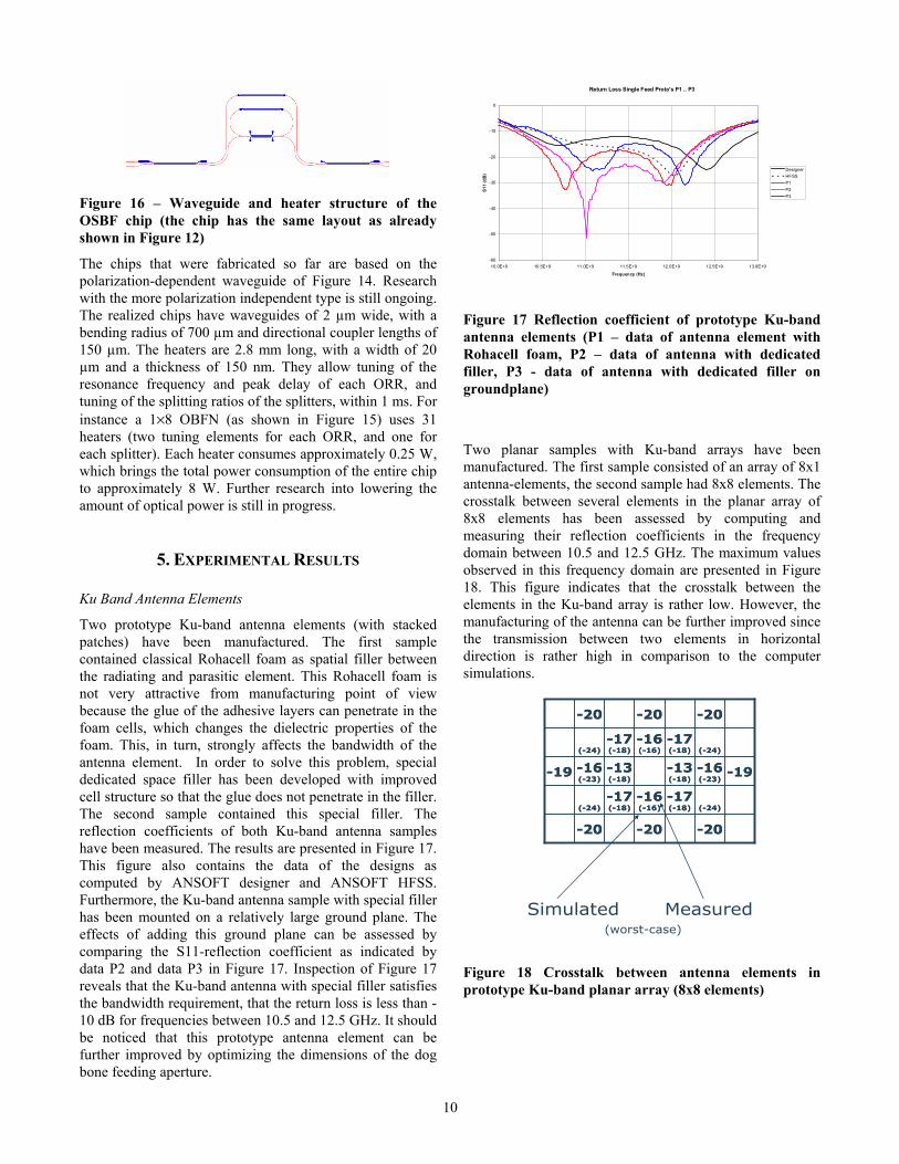
Figure 16 – Waveguide and heater structure of the OSBF chip (the chip has the same layout as already shown in Figure 12)
The chips that were fabricated so far are based on the polarization-dependent waveguide of Figure 14. Research with the more polarization independent type is still ongoing. The realized chips have waveguides of 2 µm wide, with a bending radius of 700 µm and directional coupler lengths of 150 µm. The heaters are 2.8 mm long, with a width of 20 µm and a thickness of 150 nm. They allow tuning of the resonance frequency and peak delay of each ORR, and tuning of the splitting ratios of the splitters, within 1 ms. For instance a 1×8 OBFN (as shown in Figure 15) uses 31 heaters (two tuning elements for each ORR, and one for each splitter). Each heater consumes approximately 0.25 W, which brings the total power consumption of the entire chip to approximately 8 W. Further research into lowering the amount of optical power is still in progress.
5. EXPERIMENTAL RESULTS
Ku Band Antenna Elements
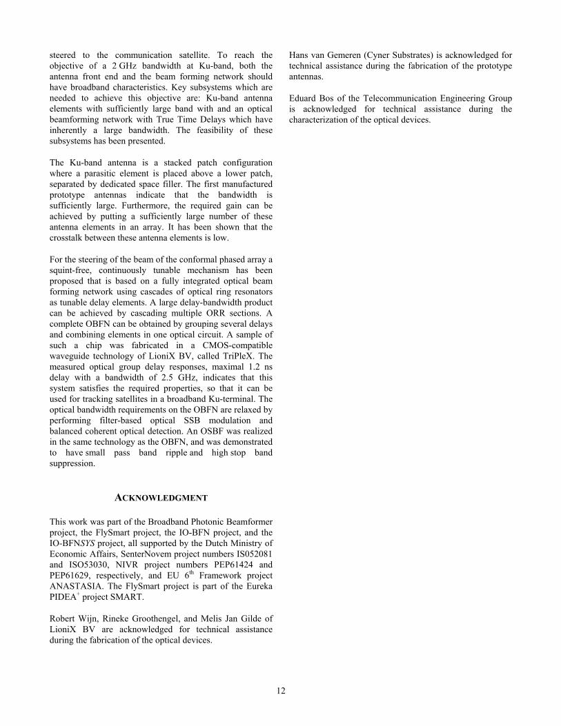
Two prototype Ku-band antenna elements (with stacked patches) have been manufactured. The first sample contained classical Rohacell foam as spatial filler between the radiating and parasitic element. This Rohacell foam is not very attractive from manufacturing point of view because the glue of the adhesive layers can penetrate in the foam cells, which changes the dielectric properties of the foam. This, in turn, strongly affects the bandwidth of the antenna element. In order to solve this problem, special dedicated space filler has been developed with improved cell structure so that the glue does not penetrate in the filler. The second sample contained this special filler. The reflection coefficients of both Ku-band antenna samples have been measured. The results are presented in Figure 17. This figure also contains the data of the designs as computed by ANSOFT designer and ANSOFT HFSS. Furthermore, the Ku-band antenna sample with special filler has been mounted on a relatively large ground plane. The effects of adding this ground plane can be assessed by comparing the S11-reflection coefficient as indicated by data P2 and data P3 in Figure 17. Inspection of Figure 17 reveals that the Ku-band antenna with special filler satisfies the bandwidth requirement, that the return loss is less than -10 dB for frequencies between 10.5 and 12.5 GHz. It should be noticed that this prototype antenna element can be further improved by optimizing the dimensions of the dog bone feeding aperture.
Return Loss Single Feed Proto's P1 .. P3
-60
-50
-40
-30
-20
-10
0
10.0E+9 10.5E+9 11.0E+9 11.5E+9 12.0E+9 12.5E+9 13.0E+9
Frequency (Hz)
S11
(dB
)
DesignerHFSSP1P2P3
Figure 17 Reflection coefficient of prototype Ku-band antenna elements (P1 – data of antenna element with Rohacell foam, P2 – data of antenna with dedicated filler, P3 - data of antenna with dedicated filler on groundplane)
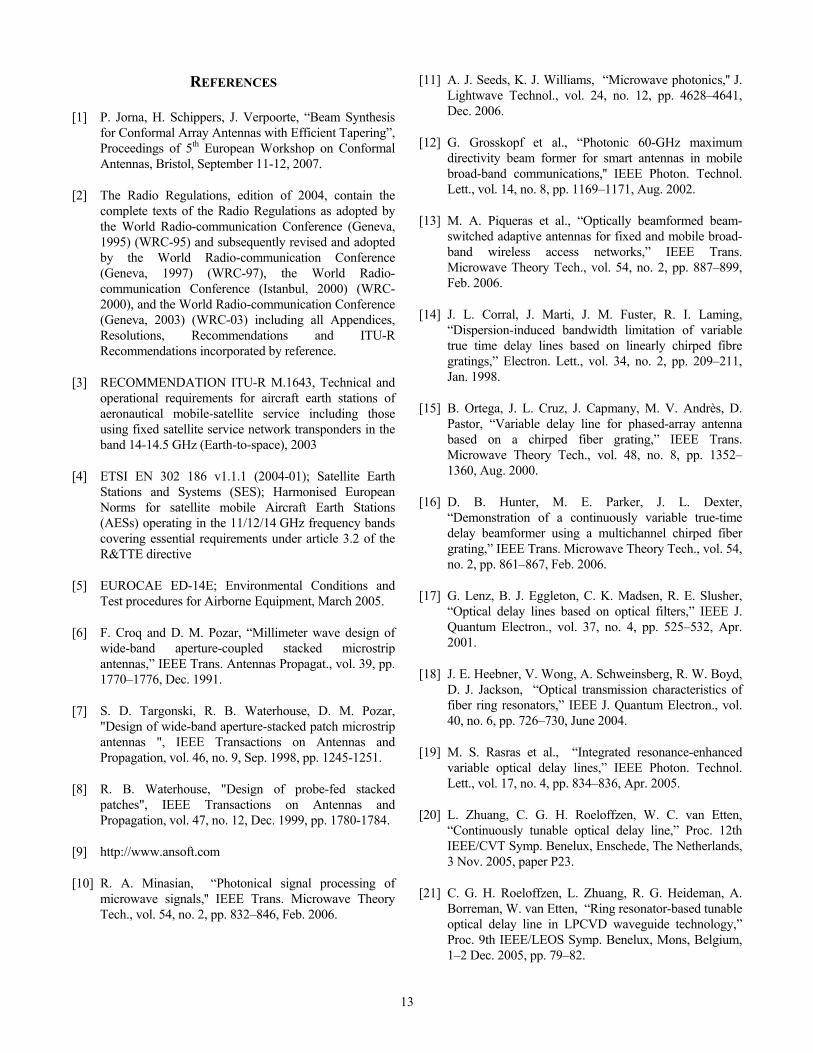
Two planar samples with Ku-band arrays have been manufactured. The first sample consisted of an array of 8x1 antenna-elements, the second sample had 8x8 elements. The crosstalk between several elements in the planar array of 8x8 elements has been assessed by computing and measuring their reflection coefficients in the frequency domain between 10.5 and 12.5 GHz. The maximum values observed in this frequency domain are presented in Figure 18. This figure indicates that the crosstalk between the elements in the Ku-band array is rather low. However, the manufacturing of the antenna can be further improved since the transmission between two elements in horizontal direction is rather high in comparison to the computer simulations.
-20-20-20
(-24)-17 (-18)
-16 (-16)
-17 (-18)(-24)
-19-16 (-23)
-13 (-18)
-13 (-18)
-16 (-23)
-19
(-24)-17 (-18)
-16 (-16)
-17 (-18)(-24)
-20-20-20
-20-20-20
(-24)-17 (-18)
-16 (-16)
-17 (-18)(-24)
-19-16 (-23)
-13 (-18)
-13 (-18)
-16 (-23)
-19
(-24)-17 (-18)
-16 (-16)
-17 (-18)(-24)
-20-20-20
MeasuredSimulated(worst-case)
Figure 18 Crosstalk between antenna elements in prototype Ku-band planar array (8x8 elements)

11
Optical Beam Forming Network Chip
The optical group delay at the outputs of the 1×8 OBFN chip were measured while varying the optical wavelength, over one FSR of 14 GHz. (This corresponds to waveguide group index of 1.8, and a ring circumference of 1.2 cm.) This was done by means of a network analyzer, using the phase shift method; details are given in [25]–[27]. The results for Output 2 to 8 are shown in Figure 19, and demonstrate the delay generation of one single ring up to seven cascaded rings, respectively. The rings are tuned such that the group delay responses are flat in a common frequency band with a width of roughly 2.5 GHz, which is more than enough to support the satellite TV band (10.7–12.75 GHz). The delay values of the respective output ports are linearly increasing, corresponding to an eight-element linear phased array. The largest delay value is approximately 1.2 ns (corresponding to 36 cm in air), and has a maximum ripple of approximately 0.1 ns (about one wavelength in Ku-band).
Note that 1.2 ns is more than enough for an eight-element linear phased array in the Ku band. These measurements were actually done within the framework of a project in which a different (lower) frequency range was considered, but clearly demonstrate that sufficient delay tuning range can be generated for satellite TV communication. Scaling to larger arrays is simply a matter of adding ports and cascading more rings to achieve higher delays.
Optical Sideband Filter Chip
Figure 20 shows the measured cross port transmission of the OSBF chip (solid line). It was normalized to the maximum power transmission in order to enable comparison to theory (dotted line), without taking into account the relatively high fiber-chip coupling losses (10 dB). These should be
attributed to the fact that this chip has no tapered end faces, so we expect to significantly improve this in the future.
From the graph we can conclude that the measured response fits in the theoretical curve rather well. We believe that the difference (especially the asymetry) should mainly be attributed to the fact the circumference of the ring might not be exactly twice the path length difference of the MZI. The pass band ripple is below 1 dB and the stop band suppression is more than 25 dB, with pass band and stop band both having a width of 15 GHz.
6. DEVELOPMENT OF DEMONSTRATOR
The demonstrator antenna that will be built in the FlySmart project will have limited capabilities compared with the airborne antenna. The main objective of the demonstrator is to show the broadband characteristics of the antenna front end and the optical beam former. In addition the beam forming and beam steering algorithms will be verified. For this purpose an 8 by 8 array antenna will be developed. In one dimension the output of all antenna elements will be coherently summed. In the other dimension the 8 combiner outputs will be fed to an 8 channel OBFN. For demonstration purposes, this antenna will be installed on a vehicle. Since the beamwidth and antenna gain are not appropriate for reception of real satellite signals, a local satellite repeater will be used for the demonstration.
7. CONCLUSIONS
For broadband satellite communication on board an aircraft the development of an advanced conformal antenna array has been discussed. Such antennas require high gain with large bandwidth of which the beam can continuously be
Wavelength (nm)
1549.97 1549.98 1549.99 1550.00 1550.01 1550.02 1550.03
Gro
up D
elay
(ns)
0.0
0.2
0.4
0.6
0.8
1.0
1.2
1.4Out 2Out 3Out 4Out 5Out 6Out 7Out 8
2.5 GHz
Max. ripple 0.1 ns
Figure 19 – Measured group delay responses at different outputs of the 1×8 OBFN chip.
~15 GHZ
~15 GHZ
> 25 dB
~15 GHZ
~15 GHZ
~15 GHZ
~15 GHZ
> 25 dB> 25 dB
Figure 20 –Normalized cross port power transmission of the OSBF chip. The solid line is the measured result, and the dotted line corresponds to the theoretical value.
12
steered to the communication satellite. To reach the objective of a 2 GHz bandwidth at Ku-band, both the antenna front end and the beam forming network should have broadband characteristics. Key subsystems which are needed to achieve this objective are: Ku-band antenna elements with sufficiently large band with and an optical beamforming network with True Time Delays which have inherently a large bandwidth. The feasibility of these subsystems has been presented.
The Ku-band antenna is a stacked patch configuration where a parasitic element is placed above a lower patch, separated by dedicated space filler. The first manufactured prototype antennas indicate that the bandwidth is sufficiently large. Furthermore, the required gain can be achieved by putting a sufficiently large number of these antenna elements in an array. It has been shown that the crosstalk between these antenna elements is low.
For the steering of the beam of the conformal phased array a squint-free, continuously tunable mechanism has been proposed that is based on a fully integrated optical beam forming network using cascades of optical ring resonators as tunable delay elements. A large delay-bandwidth product can be achieved by cascading multiple ORR sections. A complete OBFN can be obtained by grouping several delays and combining elements in one optical circuit. A sample of such a chip was fabricated in a CMOS-compatible waveguide technology of LioniX BV, called TriPleX. The measured optical group delay responses, maximal 1.2 ns delay with a bandwidth of 2.5 GHz, indicates that this system satisfies the required properties, so that it can be used for tracking satellites in a broadband Ku-terminal. The optical bandwidth requirements on the OBFN are relaxed by performing filter-based optical SSB modulation and balanced coherent optical detection. An OSBF was realized in the same technology as the OBFN, and was demonstrated to have small pass band ripple and high stop band suppression.
ACKNOWLEDGMENT
This work was part of the Broadband Photonic Beamformer project, the FlySmart project, the IO-BFN project, and the IO-BFNSYS project, all supported by the Dutch Ministry of Economic Affairs, SenterNovem project numbers IS052081 and ISO53030, NIVR project numbers PEP61424 and PEP61629, respectively, and EU 6th Framework project ANASTASIA. The FlySmart project is part of the Eureka PIDEA+ project SMART.
Robert Wijn, Rineke Groothengel, and Melis Jan Gilde of LioniX BV are acknowledged for technical assistance during the fabrication of the optical devices.
Hans van Gemeren (Cyner Substrates) is acknowledged for technical assistance during the fabrication of the prototype antennas.
Eduard Bos of the Telecommunication Engineering Group is acknowledged for technical assistance during the characterization of the optical devices.
13
REFERENCES
[1] P. Jorna, H. Schippers, J. Verpoorte, “Beam Synthesis for Conformal Array Antennas with Efficient Tapering”, Proceedings of 5th European Workshop on Conformal Antennas, Bristol, September 11-12, 2007.
[2] The Radio Regulations, edition of 2004, contain the complete texts of the Radio Regulations as adopted by the World Radio-communication Conference (Geneva, 1995) (WRC-95) and subsequently revised and adopted by the World Radio-communication Conference (Geneva, 1997) (WRC-97), the World Radio-communication Conference (Istanbul, 2000) (WRC-2000), and the World Radio-communication Conference (Geneva, 2003) (WRC-03) including all Appendices, Resolutions, Recommendations and ITU-R Recommendations incorporated by reference.
[3] RECOMMENDATION ITU-R M.1643, Technical and operational requirements for aircraft earth stations of aeronautical mobile-satellite service including those using fixed satellite service network transponders in the band 14-14.5 GHz (Earth-to-space), 2003
[4] ETSI EN 302 186 v1.1.1 (2004-01); Satellite Earth Stations and Systems (SES); Harmonised European Norms for satellite mobile Aircraft Earth Stations (AESs) operating in the 11/12/14 GHz frequency bands covering essential requirements under article 3.2 of the R&TTE directive
[5] EUROCAE ED-14E; Environmental Conditions and Test procedures for Airborne Equipment, March 2005.
[6] F. Croq and D. M. Pozar, “Millimeter wave design of wide-band aperture-coupled stacked microstrip antennas,” IEEE Trans. Antennas Propagat., vol. 39, pp. 1770–1776, Dec. 1991.
[7] S. D. Targonski, R. B. Waterhouse, D. M. Pozar, "Design of wide-band aperture-stacked patch microstrip antennas ", IEEE Transactions on Antennas and Propagation, vol. 46, no. 9, Sep. 1998, pp. 1245-1251.
[8] R. B. Waterhouse, "Design of probe-fed stacked patches", IEEE Transactions on Antennas and Propagation, vol. 47, no. 12, Dec. 1999, pp. 1780-1784.
[9] http://www.ansoft.com
[10] R. A. Minasian, “Photonical signal processing of microwave signals,'' IEEE Trans. Microwave Theory Tech., vol. 54, no. 2, pp. 832–846, Feb. 2006.
[11] A. J. Seeds, K. J. Williams, “Microwave photonics,'' J. Lightwave Technol., vol. 24, no. 12, pp. 4628–4641, Dec. 2006.
[12] G. Grosskopf et al., “Photonic 60-GHz maximum directivity beam former for smart antennas in mobile broad-band communications,'' IEEE Photon. Technol. Lett., vol. 14, no. 8, pp. 1169–1171, Aug. 2002.
[13] M. A. Piqueras et al., “Optically beamformed beam-switched adaptive antennas for fixed and mobile broad-band wireless access networks,” IEEE Trans. Microwave Theory Tech., vol. 54, no. 2, pp. 887–899, Feb. 2006.
[14] J. L. Corral, J. Marti, J. M. Fuster, R. I. Laming, “Dispersion-induced bandwidth limitation of variable true time delay lines based on linearly chirped fibre gratings,” Electron. Lett., vol. 34, no. 2, pp. 209–211, Jan. 1998.
[15] B. Ortega, J. L. Cruz, J. Capmany, M. V. Andrès, D. Pastor, “Variable delay line for phased-array antenna based on a chirped fiber grating,” IEEE Trans. Microwave Theory Tech., vol. 48, no. 8, pp. 1352–1360, Aug. 2000.
[16] D. B. Hunter, M. E. Parker, J. L. Dexter, “Demonstration of a continuously variable true-time delay beamformer using a multichannel chirped fiber grating,” IEEE Trans. Microwave Theory Tech., vol. 54, no. 2, pp. 861–867, Feb. 2006.
[17] G. Lenz, B. J. Eggleton, C. K. Madsen, R. E. Slusher, “Optical delay lines based on optical filters,” IEEE J. Quantum Electron., vol. 37, no. 4, pp. 525–532, Apr. 2001.
[18] J. E. Heebner, V. Wong, A. Schweinsberg, R. W. Boyd, D. J. Jackson, “Optical transmission characteristics of fiber ring resonators,” IEEE J. Quantum Electron., vol. 40, no. 6, pp. 726–730, June 2004.
[19] M. S. Rasras et al., “Integrated resonance-enhanced variable optical delay lines,” IEEE Photon. Technol. Lett., vol. 17, no. 4, pp. 834–836, Apr. 2005.
[20] L. Zhuang, C. G. H. Roeloffzen, W. C. van Etten, “Continuously tunable optical delay line,” Proc. 12th IEEE/CVT Symp. Benelux, Enschede, The Netherlands, 3 Nov. 2005, paper P23.
[21] C. G. H. Roeloffzen, L. Zhuang, R. G. Heideman, A. Borreman, W. van Etten, “Ring resonator-based tunable optical delay line in LPCVD waveguide technology,” Proc. 9th IEEE/LEOS Symp. Benelux, Mons, Belgium, 1–2 Dec. 2005, pp. 79–82.
14
[22] R. G. Heideman, A. Melloni, M. Hoekman, A. Borreman, A. Leinse, F. Morichetti, “Low loss, high contrast optical waveguides based on CMOS compatible LPCVD processing: technology and experimental results,” Proc. 9th IEEE/LEOS Symp. Benelux, Mons, Belgium, 1–2 Dec. 2005, pp. 71–74.
[23] R. G. Heideman, D. H. Geuzebroek, J. A. Walker, “High contrast surface waveguide technology for biochemical sensing and telecom applications,” Proc. IEEE/LEOS Annual Meeting 2006, Montreal, Canada, 29 Oct.–2 Nov. 2006, paper ThDD1.
[24] R. G. Heideman, D. H. Geuzebroek, A. Leinse, A. Melloni, F. Morichetti, C. G. H. Roeloffzen, A. Meijerink, L. Zhuang, W. van Etten, E. Klein, A. Driessen, “Low loss, high contrast optical waveguides based on CMOS compatible LPCVD processing,” Proc. 13th Europ. Conf. Integr. Opt. (ECIO'2007), Copenhagen, Denmark, 25–27 April 2007, paper WB0.
[25] L. Zhuang, C. G. H. Roeloffzen, R. G. Heideman, A. Borreman, A. Meijerink, W. van Etten, “Single-chip optical beam forming network in LPCVD waveguide technology based on optical ring resonators,” Proc. of the International Topical Meeting on Microwave Photonics (MWP'2006), Grenoble, France, 3–6 Oct. 2006, paper F1.4.
[26] L. Zhuang, C. G. H. Roeloffzen, R. G. Heideman, A. Borreman, A. Meijerink, W. van Etten, “Ring resonator-based single-chip 1 × 8 optical beam forming network in LPCVD waveguide technology,” Proc. 11th IEEE/LEOS Symp. Benelux, Eindhoven, The Netherlands, 30 Nov.–1 Dec. 2006, pp. 45–48.
[27] L. Zhuang, C. G. H. Roeloffzen, R. G. Heideman, A. Borreman, A. Meijerink, W. van Etten, “Single-chip ring resonator-based 1 × 8 optical beam forming network in CMOS-compatible waveguide technology,” IEEE Photon. Technol. Lett., vol. 15, no. 15, pp. 1130–1132, Aug. 2007.
[28] A. Meijerink, C. G. H. Roeloffzen, L. Zhuang, D. A. I. Marpaung, R. G. Heideman, A. Borreman, W. van Etten, “Phased array antenna steering using a ring resonator-based optical beam forming network,” Proc. 13th IEEE/CVT Symp. Benelux, Liège, Belgium, 23 Nov. 2006, pp. 7–12.
[29] L. Zhuang, A. Meijerink, C. G. H. Roeloffzen, D. A. I. Marpaung, J. Peña Hevilla, W. van Etten, R. G. Heideman, A. Leinse, M. Hoekman, “Phased array receive antenna steering using a ring resonator-based optical beam forming network and filter-based optical SSB-SC modulation,” Proc. of the International Topical Meeting on Microwave Photonics (MWP'2007), Victoria, BC Canada, 3–5 Oct. 2007, to be published.
[30] G. L. Abbas, V. W. S. Chan, T. K. Yee, “A dual-detector optical heterodyne receiver for local oscillator noise suppression,” J. Lightwave Technol., vol. 3, no. 5, pp. 1110–1122, Oct. 1985.
[31] R. Montgomery, R. DeSalvo, “A novel technique for double sideband suprressed carrier modulation of optical fields,” IEEE Photon. Technol. Lett., vol. 7, no. 4, pp. 434–436, Apr. 1995.
[32] K. Oda, N. Takato, H. Toba, K. Nosu, “A Wide-Band Guided-Wave Periodic Multi/Demultiplexer with Ring Resonator for Optical FDM Transmission Systems,” J. Lightwave Technol. vol. 6, no. 6. pp. 1016–1023, June 1988.
[33] R. G. Heideman, M. Hoekman, “Low modal birefringent waveguides and method of fabrication,” United States Patent US 7,146,087 B2, Dec. 5, 2006.
[34] R. G. Heideman, M. Hoekman, “Surface waveguide and method of manufacture,” United States Patent US 7,142,759 B2, Nov. 28, 2006.
[35] Phoenix BV, FlowDesigner, tool for 2D process visualization, http://www.phoenixbv.com/.
[36] D. H. Geuzebroek, A. Driessen, “Ring-resonator-based wavelength filters,” in Wavelength filters in fibre optics, H. Venghaus, Ed. Berlin: Springer, 2006, pp. 341–379.

15
BIOGRAPHIES
Harmen Schippers is senior scientist at the National Aerospace Laboratory NLR. He received his Ph. D. degree in applied mathematics from the University of Technology Delft in 1982. Since 1981 he has been employed at the National Aerospace laboratory NLR. He has research experience in computational methods
for aero-eleastics, aeroacoustic and electromagnetic problems. His current research activities are development of technology for integration of smart antennas in aircraft structures, and development of computational tools for installed antenna analysis on aircraft and spacecraft.
Jaco Verpoorte has more than 10 years research experience on antennas and propagation, Electromagnetic compatibility (EMC) and radar and satellite navigation. He is head of the EMC-laboratory of NLR. He is project manager on several projects concerning EMC-analysis and development of advanced airborne antennas.
Adriaan Hulzinga received his BEng degree in electronics from the hogeschool Windesheim in Zwolle. Since 1996 he has been employed at the National Aerospace laboratory (NLR) as a senior application engineer. He is involved in projects concerning antennas and Electromagnetic
compatibility (EMC).
Pieter Jorna received the M.Sc. degree in applied mathematics from the University of Twente in 1999. From 1999 to 2005 he was with the Laboratory of Electromagnetic Research at the University of Technology Delft. In 2005 he received the Ph.D. degree for his research on numerical computation of
electromagnetic fields in strongly inhomogeneous media. Since 2005 he is with the National Aerospace Laboratory (NLR) in the Netherlands as R&D engineer.
Arjan Meijerink was born in Almelo, The Netherlands, in 1976. He received the MSc and PhD degrees (both with honours) in electrical engineering from the University of Twente, Enschede, The Netherlands, in January 2001 and November 2005, respectively. From 2001 to 2005 he carried out research on Coherence Multiplexing for Optical
Communication Systems, in the Telecommunication Engineering Group at the University of Twente. Currently he is a postdoctoral researcher in that same group. His research interests include optical communications and RF photonic signal processing techniques, particularly optical beam forming.
Chris G. H. Roeloffzen was born in Almelo, The Netherlands, in 1973. He received the MSc degree in applied physics and PhD degree in electrical engineering from the University of Twente, Enschede, The Netherlands, in 1998 and 2002, respectively. From 1998 to 2002 he was engaged with research on integrated optical add-drop demultiplexers in Silicon
Oxinitride waveguide technology, in the Integrated Optical MicroSystems Group at the University of Twente. In 2002 he became an Assistant Professor in the Telecommunication Engineering Group at the University of Twente. He is now involved with research and education on optical fiber communications systems. His current research interests include optical communications and RF photonic signal processing techniques.
Leimeng Zhuang was born in Beijing, China, in 1980. He received the BSc degree in Telecommunication Engineering from the University of Electronic Science and Technology of China, Chengdu, China, in June 2003, and the MSc degree in electrical engineering (with honours) from the University of Twente, Enschede, The
Netherlands, in June 2005. His master thesis was about the time delay properties of optical ring resonators. He is now working towards the PhD degree in the Telecommunication Engineering Group at the University of Twente. His research is related to the development of ring resonator-based optical beam forming networks for phased array antenna systems
16
David A. I. Marpaung was born in Balikpapan, Indonesia in 1979. He received the BSc degree in physics (with honours) from Institut Teknologi Bandung, Indonesia, in February 2002, and the MSc degree in applied physics from the University of Twente, Enschede, The Netherlands, in December 2003. He is now working towards the PhD degree in the
Telecommunication Engineering Group at the University of Twente. His research is directed towards the development of efficient modulation methods to increase the dynamic range of analog optical links.
Wim van Etten was born in Zevenbergen, The Netherlands, in 1942. He received the MSc and PhD degrees in electrical engineering from Eindhoven University of Technology, Eindhoven, The Netherlands, in 1969 and 1976, respectively. From 1969 to 1970, he was with Philips Electronics, developing circuits for
oscilloscopes. In 1970, he became an Assistant Professor at Eindhoven University of Technology, Faculty of Electrical Engineering. From 1970 to 1976, he was engaged in research on the transmission of digital signals via coaxial and multiwire cables. Since 1976, he has been involved with research and education on optical fiber communications. In 1985, he was appointed Associate Professor at the Eindhoven University of Technology. In 1994, he became a Full Professor of Telecommunications at the University of Twente, Enschede, The Netherlands. His current interests comprise optical communications, mobile communications, detection, and simulation of communication systems.
René G. Heideman was born in Goor, The Netherlands, in 1965. He received the MSc and PhD degrees in applied physics from the University of Twente, Enschede, The Netherlands, in August 1988 and January 1993, respectively. After his PostDoc positions he applied his extensive know-how in
the industry. Since 2001, he is co-founder and CTO of LioniX BV, Enschede, The Netherlands. He is an expert in the field of MST, in which he has more than 20 years of experience. He specializes in Integrated Optics, covering both (bio-)chemical sensing and telecom applications.
Albert Borreman was born in Wapenveld, The Netherlands, in 1969. He received the MSc degree in applied physics and the MTD degree in integrated optics from the University of Twente, Enschede, The Netherlands, in 1993 and 1996, respectively. He joined the Photonic Research group of Akzo Nobel in Arnhem, The Netherlands, in 1996
where he participated in the development of polymeric optical switches. From 1998 to 2001 he was with JDS-Uniphase Optical Switch group in Arnhem, The Netherlands. In 2002 he joined the Integrated Optical MicroSystems group of the University of Twente, where he was working on multimode polymeric optical devices. From 2003 to 2007 he was with Lionix BV, Enschede, The Netherlands, where he was involved in the development of microsystem-based optical components, with particular interest in design, fabrication, and assembly of LSI photonics devices. He is now working for Helianthos (a Nuon Company), Arnhem, The Netherlands, developing solar cells based on thin films.
Arne Leinse was born in Enschede, the Netherlands, in 1977 and studied applied physics at the University of Twente where he received a M.Sc. degree at the integrated Optical Microsystems group in 2001. In this same group he started his PhD work on the topic of active microring resonators for various optical
applications. His PhD work was carried out in the framework of a European project (IST 2000-28018 “Next generation Active Integrated optic Sub-systems”) and his thesis was titled: “Polymeric microring resonator based electro-optic modulator". In 2005 he joined LioniX BV where he is now involved as a project engineer in several integrated optical projects.
17
Marcel Hoekman studied Applied physics at the University of Twente and graduated at the Integrated Optical Micro Systems group in 1998. In 2001 he finished a post graduate design program at the Integrated Optical Micro Systems group that was based on the design of an integrated optical electro-optical modulator based on PZT
containing multilayer-stacks. In this project he worked together with the group Experimental Solid State Physics III of Radboud University Nijmegen. In 2001 he joined Lion Photonix Technologies BV – which is called LioniX BV since 2002 – as design engineer. Besides simulation and mask design he has experience in several cleanroom manufacturing processes and characterisation methods, and he has worked as project leader on several projects. Since 2004 he is a part-time PhD student at the Integrated Optical Micro Systems group in the framework of the STW project “Multi-Sensing Arrays of Separately Accessible Optics Sensors”.
Marc Wintels was graduated in business administration. Then he fulfilled several commercial and financial jobs. With this background he became an entrepreneurial partner in a PCB manufacturing company, of which he became full owner several years later. From the beginning Cyner substrates had its focus on the production of
prototyping and non-conventional Printed Circuit boards. Working mainly for design and research centers Cyner got involved in many high tech projects and from this developed a great expertise in the use of different (RF) materials. In the FlySmart project Marc and his colleagues are able to do what they like most: In close cooperation with designers, creatively working on substrate solutions.