Bridging Design and Prototype with LabVIEW ...3gpptrend.cm.nctu.edu.tw/04. Bridging Design...
32
ni.com Bridging Design and Prototype with LabVIEW Communications System Design Suite Erik Luther [email protected] Product Marketing Software Defined Radio
-
Upload
vuongxuyen -
Category
Documents
-
view
242 -
download
5
Transcript of Bridging Design and Prototype with LabVIEW ...3gpptrend.cm.nctu.edu.tw/04. Bridging Design...

ni.com
Bridging Design and Prototype with LabVIEW Communications System Design Suite
Erik Luther
Product Marketing
Software Defined Radio

ni.com
SDR Algorithm Prototyping Applications
Utilities & Infrastructure
Medical Devices & Internet of Things
Aerospace & Defense
Automotive & Car to Car
Communications & RF Identification
Research Topics
Data rate
Capacity
Power Consumption
Coexistence
Security
Monitoring
Land Mobile & Safety Radio
Satellite Comm & Navigation
Education

ni.com
TCAS High gain SATCOM
Low-gain VHF
Xpndr
VHF
DME ADF EPIRB Marker RADAR Altimeter
HF

ni.com
A Typical 747 has…
• 2 x 400 W voice HF
• 3 x 25 W voice/data VHF
• 2 x 100 W 9GHz RADARs
• 2 x GPS, 1.5GHz 60 W voice/data SATCOM
• 2 x 75MHz marker beacons
• 3 x VHF LOC localiser
• 3 x UHF glide slope
• 2 x LF ADF automatic direction finder
• 2 x VOR VHF omni-directional range
• 2 x 1GHz 600 W transponders
• 2 x 1GHz 700 W DME distance measuring equipment
• 3 x 500mW 4.3GHz radar altimeters
• 3 x 406MHz EPIRB
31 radios

ni.com
GPS Simulation
Things to Simulate • Poor signal strength
• View of satellites obstructed
• Position constantly changing
NI USRP-2920 Generates Signal
GPS Toolkit Creates Signal in LabVIEW
GPS Receiver
GPS receiver behaves as if it sees real satellites
Precision Clock (10 MHz OCXO)

ni.com
NI SDR Hardware Platforms
FlexRIO, NI 579x Features • Frequency Range: 200 MHz to 4.4 GHz (aligned) • FPGA: Kintex 7 410T • Bandwidth: 100 MHz / 200 MHz • Host I/F: PXIe x4 (~800 MB/s) • Calibration: Minimal, System
USRP RIO 294x/5x Features • Frequency Range: 50 MHz to 6 GHz (coherent) • FPGA: Kintex 7 410T • Bandwidth: 40 MHz bandwidth • Host I/F: PXIe x4 (~800 MB/s) • Calibration: Minimal, System
USRP 292x/3x Features • Frequency Range: 50 MHz to 6 GHz (coherent) • FPGA: Host processing • Bandwidth: 20 MHz bandwidth • Host I/F: 1 Gb Ethernet (100 MB/s) • Calibration: None, User

ni.com
Massive MIMO – Algorithms & Software
• OFDM PHY processing at each radio head
• Sub-channels streamed to /from FlexRIO for MIMO
• Precoding applied with low latency P2P connection
• MAC processing on the host controller
Ma
ste
r
PXIe-8135
PXIe-7976R FPGA (1-8)
MIMO RX
...
MAC (Medium Access Control)
BER Calculator Source Data
USRP RIO
2x2 (1)
OF
DM
TX
OF
DM
RX
MIMO TX
USRP RIO
2x2 (64)
OF
DM
TX
OF
DM
RX
Precoding
USRP RIO
2x2 (2)
OF
DM
TX
OF
DM
RX
Antennas 1-128

ni.com
Classic Tool Flow
• Disaggregate tools
• Many specializations
• Longer design cycles
• Increased time to result

ni.com
Platform-Based Design for System on a Chip
A. Sangiovanni-Vincentelli, UC Berkeley. Defining Platform Based Design. EEDesign, Feb 2002

ni.com
A Platform Revolutionizes Your Approach to Solutions

ni.com
Why Do Ecosystems Win? 1 Million Apps, 1,000/Day

ni.com
Graphical System Design Approach for Communication System Prototyping
PHY Cognitive MIMO mmWave Next Gen
USRP USRP RIO Flex RIO VST

ni.com
Commitment to Streamlining the Design Flow
Investing in accelerating productivity with LabVIEW:
• Mapping algorithms across processors
• Context aware float-to-fixed conversion
• Integration of custom IP such as .m, C, HDL
• Code sharing across traditional hardware boundaries
Faster time to prototype “rapid prototyping”

ni.com
The Ideal Solution One continuous design flow that unifies the disparate design teams
Single, Cohesive Toolchain
System Mapping System Implementation Algorithm Development
Collaborative Design Team
Iterative Modeling
Rapid hardware mapping
exploration

ni.com
Develop on the Host (All NI USRP Devices)
Example: OFDM Transmitter
• Describe the algorithm graphically
• Combine models of computation
• Seamlessly integrate I/O

ni.com
Algorithm Design Languages: Processor
• Flexible design approach with dataflow (G), and text nodes for C and .m
• Text Nodes for C and .m support syntax highlighting and function completion
• Both G and the Text Nodes support full debugging with breakpoints and probes
C node
.m node
G

ni.com
NI USRP RIO Driver Software (Host + FPGA)
LabVIEW (Host PC) LabVIEW FPGA (FPGA) RF
DMA FIFO
(PCIe x4)
ADC
ADC
PLL
I
Q
Impairment Correction
Frequency Shift
Fractional Decimator
Impairment Correction
Frequency Shift
Fractional Interpolator
DMA FIFO
(PCIe x4)
DAC
DAC
PLL
I
Q
120 MHz Data Clock
OFDM Receiver
OFDM Transmitter
Your Code Here
Your Code Here
Your Host Code Here
Your Host Code Here
Rx
Tx
Cabled PCIe USRP RIO PC or Laptop
ni.com
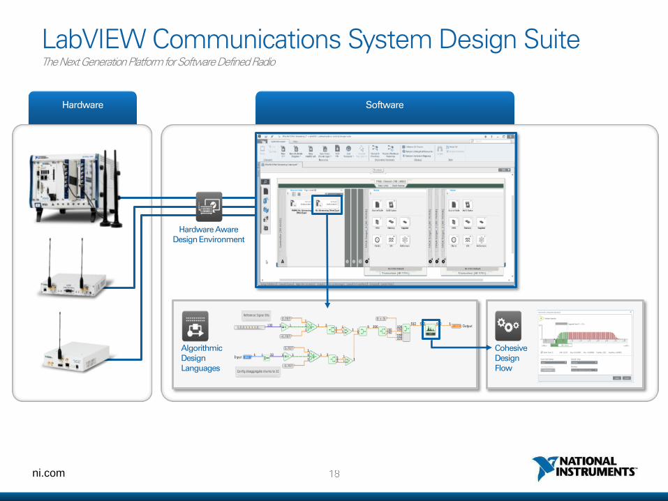
LabVIEW Communications System Design Suite The Next Generation Platform for Software Defined Radio
Hardware Software
Hardware Aware Design Environment
Algorithmic Design Languages
Cohesive Design Flow

ni.com
Unified Design Flow
Single, Cohesive Toolchain
System Mapping Design Exploration System Implementation Algorithm Development
C and .M Support
Algorithm design languages
Hardware aware environment
Easy, iterative design
partitioning
Design simulation tools built in
Analyze tradeoffs in
implementations
Deploy to hardware with one
click
Prototype with real-world
signals
Collaborative Design Team

ni.com
Hardware-Aware Design Environment System Throughput
and Latency
Hardware management
Source Code Management &
Synchronized Execution
Interactive, visual
representation of
the physical
system which:
• Enables system discovery and verification of system setup
• Provides hardware documentation and visualization of available resources
• Allows for design partitioning and deployment
• Enables articulation of system architecture

ni.com
Algorithm Design Languages: Processor
• Flexible design approach with dataflow (G), and text nodes for C and .m
• Text Nodes for C and .m support syntax highlighting and function completion
• Both G and the Text Nodes support full debugging with breakpoints and probes
C node
.m node
G

ni.com
Quickly Deploy Ideas to FPGA
Multirate Diagram • Ideal start for Algorithm Prototyping • Signal Processing IP Stitching
FPGA IP • Dataflow (G) algorithm design • Transition designs from host to FPGA
Clock Driven Logic* • Low-level optimization • Precise timing control
Mapping &
Optimization
FPGA
*previously called “single cycle timed loop”

ni.com
Textbook Example: OFDM Transmitter
5 MHz, LTE-Like Design
• Symbol Mapping: 4 QAM
• Data/Pilot Structure: 1 Pilot for every 5 Data Symbols
• Frame Structure: 512 Elements [106 Zeros, 150 Data/Pilot, 1 Zero, 150 Data/Pilot, 105 Zeros]
• Cyclic Prefix Length: 128
Data In
Pilot Symbols In
Map to Symbols
Interleave Pilot & Data
Symbols
Zero Padding
IFFT Cyclic Prefix
Tx

ni.com
Mulitrate Design Exploration
Float to Fixed Analysis & Histogram
Intuitive multi-rate DSP Design
Static scheduling & pipelining based on
throughput & latency constraints

ni.com
System Implementation
Sample Projects: source code to start your design
• Synchronization and Timing Control across multiple RF Front-Ends & FPGAs
• Corrected RF, Arbitrary Rate Conversion, Frequency Shift
FlexRIO (Xilinx 7 Series) & 579x RF Adapters*
NI USRP (292x/293x)
NI USRP RIO (294x/295x)
* Check FAQ for list of supported FlexRIO HW

ni.com
LTE & 802.11 Application Frameworks Ready-to-Run Standards-Based Source Code Implementations
PH
Y
Transmitter Receiver
RF Hardware
RF Down
ADC
FPGA
RF Impairments Correction
Time/Freq. Synchronization
LTE OFDM Demodulation
LTE Channel Decoder
Host
Rx UDP Socket
Improved Noise Cancellation
Host FPGA RF Hardware
RF Up DAC RF Impairments
Correction LTE OFDM Modulation
LTE Channel Encoder
Tx UDP Socket
New Waveform Research
IEEE 802.11 OFDM Physical Layer • SISO Configuration • 20 MHz Bandwidth with up to 64 QAM • Training Field Based Packet Detection & Signal
Field Detection • Channel Encoding and Decoding
IEEE 802.11 lower MAC Layer • Multi-Node Addressing • CRC and Frame Type Check • ACK Generation with 802.11 Approximated
SIFS Timing
3GPP-LTE Downlink Physical Layer • SISO Configuration • 20 MHz Bandwidth TDD Frame Structure • LTE Channel Encoding and Decoding • Control & Data Channel (PDCCH & PDSCH) • Up to 60 Mbps • Cell-specific and UE Specific Reference
Signals • Primary Synchronization Signal
Available
Now!

ni.com
LTE and 802.11 Application Frameworks Real-time wireless system implementation
• Ready to run PHY and basic MAC
• Communicate between devices or in loop-back mode
Modular Open Source Design
• ~50% of FPGA resources available for customization
• Replace existing blocks with your own waveform designs
Fastest path from algorithm to prototype
• Single language for host and FPGA design in LabVIEW
• Documented for ease of use and understanding
Applications • Customized LTE and 802.11 applications
• LTE and 802.11 coexistence research testbed
• 5G new waveform research with real prototyping

ni.com
Community Contributed Reference Designs
8x8 MIMO-OFDM GPS Simulation
ADS-B Monitoring & Decoding
RF Direction Finding & Localization
Tx
ni.com/sdr

ni.com
NI 5791 Tx/Rx 100 MHz BW
• Rapid Prototyping
• Wireless Link
NI 5792 Rx 200 MHz BW
• Spectrum monitoring
• Advanced prototyping
NI 5793 Tx 200 MHz BW
• Wideband generator
• Advanced prototyping
NI 579x RF Transceiver Adapter Module
Target applications
• Software-defined radio (SDR)
• High-performance embedded systems
• MIMO / multi-channel, phase-coherent measurements
• Prototyping wide bandwidth next generation standards (802.11ac)
Features
• 200 MHz – 4.4 GHz RF Frequency
• Direct up and downconversion
• 130/250 MS/s, 14-bit input, 16-bit output
• 12 DIO for digital control

ni.com
Teaching Next Generation of Wireless Engineers

ni.com
“The course evaluations for our class were fantastic! Students rated the class 4.94/5.0, likely making it one of the highest rated among all classes in the School of Engineering at Stanford.”
–Dr. Sachin Katti, Stanford University
“Hands down the best EE class I’ve taken so far.”
–Student “Awesome class! I really enjoyed the lectures, and the labs were really cool because we got to use the hardware.”
–Student
Teaching Next Generation of Wireless Engineers

ni.com
Summary
• Platform based design accelerates system design
• Models of computation allow multiple design approaches.
• The right tools can accelerate innovation with SDR.
Learn more at: ni.com/sdr