BRAKE DETERIORATION INDICATOR - University of...
40
UNIVERSITY OF NAIROBI BRAKE DETERIORATION INDICATOR PRJ 074 BY GITHINJI BLASIO IKUNDO F17/1748/2006 SUPERVISOR: DR. G. KAMUCHA EXAMINER: DR. MWANGI MBUTHIA Project report submitted in partial fulfillment of the requirement for the award degree of Bachelor of Science in Electrical and Electronic Engineering of the University of Nairobi Date of submission: 18 th may, 2011 DEPARTMENT OF ELECTRICAL AND INFORMATION ENGINEERING
Transcript of BRAKE DETERIORATION INDICATOR - University of...

UNIVERSITY OF NAIROBI
BRAKE DETERIORATION INDICATOR
PRJ 074
BY
GITHINJI BLASIO IKUNDO
F17/1748/2006
SUPERVISOR: DR. G. KAMUCHA
EXAMINER: DR. MWANGI MBUTHIA
Project report submitted in partial fulfillment of the requirement for the award degree of
Bachelor of Science in Electrical and Electronic Engineering of the University of Nairobi
Date of submission:
18th may, 2011
DEPARTMENT OF ELECTRICAL AND INFORMATION ENGINEERING

ii
DEDICATION
This work is dedicated to my parents and friends for their faith and support in my education.

iii
ACKNOWLEDGEMENTS
I would like to extend my sincere thanks to all the people who gave generously their time.
Firstly, my supervisor Dr. Kamucha for the guidance he gave me through every stage of the
project, from initial conception to final implementation of the circuit.
Secondly, to the Muhoro’s, the Kamere’s and aunt Wangui for supporting me to realize my
dream academically
Thirdly, to my parents and family member’s for their tireless encouragement, moral and financial
support during this period, I do appreciate.
Lastly, to my Fiancé, Susan, gratitude for her moral support and understanding when I was
buried in the project work.
Sincerely, I have learnt a lot through this entire period.
Thank you all and may God bless you abundantly.
Suggestions, comments and critiques are welcomed and may be addressed to;
GITHINJI BLASIO IKUNDO
P.O BOX 605-00100,
NAIROBI,
KENYA
EMAIL;[email protected]

iv
DECLARATION
This report is presented in partial fulfillment of the requirements for the degree of Bachelor of
Science Electrical and Electronic Engineering.
It is entirely my original work and has not been submitted to any other University or higher
education institution or for any other academic award.
Where use has been made of the work of other people it has been fully acknowledged and fully
referenced.
Signature:
………………………………………..
GITHINJI BLASIO IKUNDO
F17/1748/2006
This report has been submitted to the Department of Electrical and Information Engineering,
University of Nairobi with my approval as supervisor:
Signature:
………………………………
DR. KAMUCHA
Date…………………………….

v
ABSTRACT
The braking system is one of several key safety-related items. Catastrophic brake failure, such
as sudden air loss, may lead to loss of control and the driver’s inability to recover. Progressive
brake deterioration, such as brake shoe wear without corresponding adjustment, can be even
more troublesome because it may appear innocuous during normal driving, but may precipitate
an accident during emergency braking applications. When brakes are malfunctioning sometimes
the driver may not realize and this may endanger the life of the people on board and other road
users. Statistics shows that lots of lives are lost in road accidents and to some extent the brakes
failed to function as expected by the driver. This arouses interest in getting a way of notifying the
driver about the performance of the brakes. The design of ‘Brake deterioration indicator’ comes
in play to bridge this lack.
The working of the vehicle’s braking system is given in the theory whereas in the design the
brake system interface to the designed circuitry is a potentiometer which is assumed to vary
directly as the brake performance varies.

vi
TABLE OF CONTENTS
DEDICATION ........................................................................................................................ II
ACKNOWLEDGEMENTS ................................................................................................... III
DECLARATION .................................................................................................................... IV
ABSTRACT.............................................................................................................................. V
TABLE OF CONTENTS ....................................................................................................... VI
LIST OF FIGURES ............................................................................................................ VIII
CHAPTER 1 ..............................................................................................................................1
1.0 INTRODUCTION .......................................................................................................................................... 1 1.1 PROJECT OBJECTIVE ................................................................................................................................ 1 1.2 BACKGROUND OF VEHICLE’S BRAKING SYSTEM: ............................................................................. 1
1.2.1 Characteristics of Materials for brake lining: ........................................................................................ 1 1.2.2 Types of brakes: .................................................................................................................................... 1 1.2.3 Types of vehicle brakes: ......................................................................................................................... 2 1.2.4 Hydraulic Principles.............................................................................................................................. 3 1.2.5 Hydraulics............................................................................................................................................. 4 1.2.6 Brake pedal design ................................................................................................................................ 5 1.2.7 Brake fluid ............................................................................................................................................ 6 1.2.8 Master cylinder ..................................................................................................................................... 7 1.2.9 Drum brakes.......................................................................................................................................... 7 1.2.10 Caliper types ....................................................................................................................................... 8 1.2.11 Diagnosis .......................................................................................................................................... 10
CHAPTER 2 ............................................................................................................................ 11
2.1 DESIGN OVERVIEW ......................................................................................................................................... 11 2.1.1 Voltage regulator stage: ...................................................................................................................... 11 2.1.2 The Comparator stage ......................................................................................................................... 18 2.1.3 The output stage .................................................................................................................................. 22
CHAPTER 3 ............................................................................................................................ 28
3.1DESIGN RESULTS ....................................................................................................................................... 28 3.1.1 Voltage regulator results: .................................................................................................................... 28 3.1.2 Comparator and output stages’ results ................................................................................................. 28
CHAPTER 4 ............................................................................................................................ 29
RECOMMENDATIONS AND CONCLUSION ............................................... ERROR! BOOKMARK NOT DEFINED. 5.1 CONCLUSION ............................................................................................................................................. 29 5.2 RECOMMENDATIONS .............................................................................................................................. 29
APPENDIX A .......................................................................................................................... 30
APPENDIX B .......................................................................................................................... 31
REFFERENCES ..................................................................................................................... 32

vii

viii
LIST OF FIGURES
Figure 1 Typical parking brakes. .................................................................................................2 Figure 2 typical brake system ......................................................................................................3 Figure 3 Simplified Hydraulic Brake Syste..................................................................................4 Figure 4 Distribution of hydraulic pressure. .................................................................................4 Figure 5Same line pressure to all wheels. ....................................................................................5 Figure 6 pedal design model ........................................................................................................6 Figure 7 master cylinder diagram. ...............................................................................................7 Figure 8 brake drum. ...................................................................................................................8 Figure 9 Fixed Caliper.................................................................................................................8 Figure 10 Fixed Caliper elaborated ..............................................................................................9 Figure 11 Sliding Caliper ............................................................................................................9 Figure 12 diagram showing angle Ө as the pedal travel ............................................................ 10 Figure 13 a Simple Op-Amp-based Voltage Regulator Circuit................................................... 12 Figure 14 Transistor (PNP) and (NPN) ...................................................................................... 13 Figure 15 npn common emitter characteristics ........................................................................... 13 Figure 16 characteristics of Zener diode ................................................................................. 15 Figure 17 zener diode voltage ................................................................................................. 15 Figure 18 Comparator Response to Noisy Inputs ....................................................................... 19 Figure 19 comparator with a positive feedback. ......................................................................... 19 Figure 20 diagram showing hysteresis .................................................................................... 21 Figure 21 diagram showing how Comparator with Schmitt Trigger Respond to Noisy Inputs .... 21 Figure 22 Block Diagram for a 555 Timer ................................................................................. 22 Figure 23 Schematic of a 555 Timer in Oscillator Mode ............................................................ 23 Figure 24 tHIGH : Calculations for the Oscillator’s HIGH Time .................................................. 23 Figure 25 tLOW : Calculations for the Oscillator’s LOW Time .................................................... 24 Figure 26 parts of an LED ......................................................................................................... 25 Figure 27 I-V characteristics for a diode. ................................................................................... 26
1
CHAPTER 1
1.0 INTRODUCTION
1.1 PROJECT OBJECTIVE
To Design and implement a system that will warn the driver when the vehicle braking system is
failing using both audio and visual warnings.
1.2 BACKGROUND OF VEHICLE’S BRAKING SYSTEM:
Brake is a device by means of which artificial friction as resistance is applied to a moving
machine member, in order to retard or stop the motion of a machine.
Capacity of brake depends on:
• The unit pressure between the braking surfaces
• The coefficient of friction between the braking surfaces.
• The peripheral velocity of the brake drum.
• The projected area of the friction surfaces
• The ability of the brake to dissipate heat equivalent to the energy being absorbed.
1.2.1 Characteristics of Materials for brake lining:
• Coefficient of friction should remain constant with change in temperature.
• Have low wear rate
• Have high heat resistance
• High heat dissipation capacity
• Have adequate mechanical strength
• Shouldn’t be affected by moisture and oil.
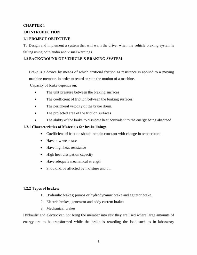
1.2.2 Types of brakes:
1. Hydraulic brakes; pumps or hydrodynamic brake and agitator brake.
2. Electric brakes; generator and eddy current brakes
3. Mechanical brakes
Hydraulic and electric can not bring the member into rest they are used where large amounts of
energy are to be transformed while the brake is retarding the load such as in laboratory

2
dynamometers, highway trucks and electric locomotives. These brakes are also used to control
the speed or retarding the speed of a vehicle for downhill travel.
1.2.3 Types of vehicle brakes:
We have two types of braking systems namely:
1. Parking Brake
2. Service Brake; this type of braking system is sub-divided into two categories:
a) Hydraulic
i. Disc Brakes
ii. Drum Brakes
iii. Dual System
b) Antilock Brake System (ABS)
1.2.3.1 Parking brakes:
These are not used for “Emergency” Braking they are used specifically to keep a parked vehicle
from moving and are usually on rear wheels only. They are mechanically operated
Figure 1 Typical parking brakes.

3
1.2.3.2 Service brakes:
These are usually the primary Braking System and should be stronger than the engine. They are
Hydraulic Operated.
Ø Can be Vacuum, Hydro or Motor assisted
Ø Disc System
Ø Drum System
Ø Dual System
Figure 2 typical brake system
1.2.4 Hydraulic Principles
Breaking system uses fluids since they have the following characteristics:
Ø Fluids cannot be compressed
Ø Fluids can transmit Movement

4
Ø Acts “Like a steel rod” in a closed container
Ø Master cylinder transmits fluid to wheel cylinder or caliper piston bore.
Ø Fluids can transmit and increase force
���������
� �������� (1.1)
1.2.5 Hydraulics
Figure 3 shows a simplified braking system modeled for the understanding of hydraulics.
Ø Drum Brake
Ø Master Cylinder
Ø Disk Brake
Figure 3 Simplified Hydraulic Brake Syste
Hydraulic pressure is distributed equally in all directions as shown in figure 4
Figure 4 Distribution of hydraulic pressure.
5
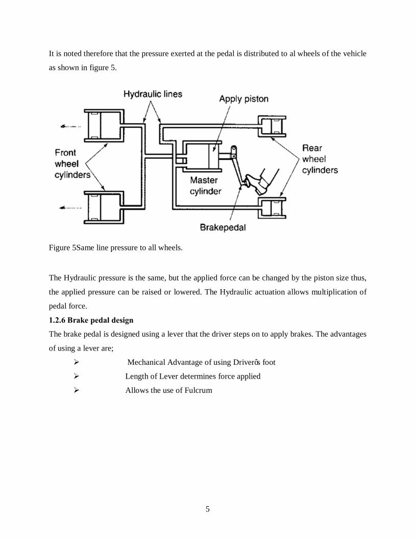
It is noted therefore that the pressure exerted at the pedal is distributed to al wheels of the vehicle
as shown in figure 5.
Figure 5Same line pressure to all wheels.
The Hydraulic pressure is the same, but the applied force can be changed by the piston size thus,
the applied pressure can be raised or lowered. The Hydraulic actuation allows multiplication of
pedal force.
1.2.6 Brake pedal design
The brake pedal is designed using a lever that the driver steps on to apply brakes. The advantages
of using a lever are;
Ø Mechanical Advantage of using Driver’s foot
Ø Length of Lever determines force applied
Ø Allows the use of Fulcrum

6
Figure 6 pedal design model
The Pedal Ratio is given by; ���
� �: � (1.2)
1.2.7 Brake fluid
1.2.7.1 Brake fluid properties
Ø Does not thicken or thin with changing heat
Ø Must not boil
Ø Must be compatible with brake parts material
Ø Must lubricate internal parts
Ø Must not evaporate easily
1.2.7.2 Brake fluid contaminates
Ø Moister- Lowers boiling point; water boils @ 212*F DOT 3 boils @
401*F
Ø Petroleum Based Product- soften rubber parts causing swelling
Ø Dirt & Debris- causes corrosion and clogs
Ø Air and Vapors- air is Compressible hence prevents pressure from
reaching brakes

7
1.2.8 Master cylinder
Figure 7 master cylinder diagram.
The Master cylinder provides a reservoir for brake fluid and contains the driving pistons in the
hydraulic circuit. There are two types of master cylinders:
• Front - Rear split -One piston for front brakes and one for rear
• Diagonally split -One piston drives one front wheel and one rear wheel.
These layouts allows one to maintain directional control incase of leakage.
1.2.9 Drum brakes
In drum brakes, expanding shoes create force on the inner surface of the drum. They are
normally used on the rear of some trucks. Self-energizing design requires less activation force
though it requires periodic adjustment.

8
Figure 8 brake drum.
1.2.10 Caliper types
There are 2 types of Calipers
Ø Fixed: these are disc brakes that use a caliper that is FIXED in position
and does not slide. They have pistons on both sides of the disc. There may be 2 or 4
pistons per caliper. Motorcycles and some import trucks and cars use this type, they are
similar to bicycle brakes
Figure 9 Fixed Caliper

9
Figure 10 Fixed Caliper elaborated
Fixed calipers apply two pistons to opposite sides of rotor, the caliper stays stationary and the
disc brakes require higher hydraulic pressure.
Ø Floating: these are much more common; they have single Piston and are
easier to work with. They are mounted on “inboard” side of caliper
Figure 11 Sliding Caliper
Sliding caliper applies pressure to two pads on opposite sides of rotor.

10
1.2.11 Diagnosis
Several different types of Complaints on brake failure:
1.2.11.1 Noise
This may be caused by wearing out of break pads. In this case, we may use Wear
Indicator to indicate the extent of brake deterioration. It is worthwhile noting that some
break pads that use semi-metallic pads do produce screeching sound and this should not
be mistaken for brake failure.
1.2.11.2 Pulsation
Usually caused by a warped Rotor. When the brakes are applied, one feels pulsation
through the brake pedal and even the steering wheel. The rotor can be repaired or made
“true” on a machine that smoothens the rotor.
1.2.11.3 Pedal travel
The excessive pedal travel and Pedal feeling soft and squishy is an indication of brake
deterioration. When the brake pedal travels much then one requires excessive effort to
stop vehicle or my cause brakes to not function at all.
Figure 12 diagram showing angle Ө as the pedal travel

11
CHAPTER 2
2.1 Design overview
The design of the brake deterioration indicator is designed in three phases namely;
1. The voltage regulator stage; – this gives a regulated output voltage from the
normally fluctuating supply hereby taken from the vehicle’s lead acid battery.
2. The comparators stage; – this phase utilizes three comparators to compare
voltages at three set points. They give a judgment on the functionality of the brakes. The
brake interface is replaced with a potentiometer – as the pedal travel angle increases, the
contact is modeled in a way that the potentiometer resistance increases in direct
proportion. R∞Ө (where R is resistance and Ө is the pedal travel angle).
3. The output stage; – this is facilitated using display diodes (LED) and a buzzer.
Three diodes are used to display different performance of the brakes. Green for well
functioning, yellow for fairly functioning and red colored for poor functioning. In
conjunction with the red diode, a buzzer buzzes to emphasis the poor functionality
2.1.1 Voltage regulator stage:
Voltage regulator is any electrical or electronic device that maintains the voltage of a power
source within acceptable limits. The voltage regulator is needed to keep voltages within the
prescribed range that can be tolerated by the electrical equipment using that voltage.

12
Figure 13 a Simple Op-Amp-based Voltage Regulator Circuit.
The following components are used to design a voltage regulator:
1. Transistor
2. Zener diode
3. Operational amplifier (discussed in section 2.1.2)
2.1.1.1 Bipolar Junction Transistors
The bipolar junction transistor (BJT) is the salient invention that led to the electronic age,
integrated circuits, and ultimately the entire digital world. The transistor is the principal active
device in electrical circuits. When inputs are kept relatively small, the transistor serves as an
amplifier. When the transistor is overdriven, it acts as a switch, a mode most useful in digital
electronics

13
Figure 14 Transistor (PNP) and (NPN)
Figure 15 npn common emitter characteristics
A bipolar transistor consists of a three-layer “sandwich” of doped (extrinsic) semiconductor
materials, either P-N-P or N-P-N. The only functional difference between a PNP transistor and
an NPN transistor is the proper biasing (polarity) of the junctions when operating. For any given
state of operation, the current directions and voltage polarities for each type of transistor are
exactly opposite each other. Bipolar transistors work as current-controlled current regulators. In
other words, they restrict the amount of current that can go through them according to a smaller,
controlling current. The main current that is controlled goes from collector to emitter, or from
emitter to collector, depending on the type of transistor it is (PNP or NPN, respectively). The
small current that controls the main current goes from base to emitter or from emitter to base,

14
once again depending on the type of transistor it is (PNP or NPN, respectively). Bipolar
transistors are called bipolar because the main flow of electrons through them takes place in two
types of semiconductor material: P and N, as the main current go from emitter to collector (or
vice versa). In other words, two types of charge carriers “electrons and holes “comprise this main
current through the transistor. The controlling current and the controlled current always mesh
together through the emitter wire, and their electrons always flow against the direction of the
transistor's arrow. This is the first and foremost rule in the use of transistors: all currents must be
going in the proper directions for the device to work as a current regulator. The small, controlling
current is usually referred to simply as the base current because it is the only current that goes
through the base wire of the transistor. Conversely, the large, controlled current is referred to as
the collector current because it is the only current that goes through the collector wire. The
emitter current is the sum of the base and collector currents, in compliance with Kirchhoff's
Current Law if there is no current through the base of the transistor; it shuts off like an open
switch and prevents current through the collector. If there is a base current, then the transistor
turns on like a closed switch and allows a proportional amount of current through the collector.
Collector current is primarily limited by the base current, regardless of the amount of voltage
available to push it. Because a transistor's collector current is proportionally limited by its base
current, it can be used as a sort of current-controlled switch. A relatively small flow of electrons
sent through the base of the transistor has the ability to exert control over a much larger flow of
electrons through the collector [1]
Characteristics of Transistors:
• Cutoff Region
In this region there is no enough voltage at B for the diode to turn on, thus no current
flows from C to E and the voltage at C is Vcc.
• Saturation Region
The voltage at B exceeds 0.7 volts, the diode turns on and the maximum amount of
current flows from C to E. The voltage drop from C to E in this region is about 0.2V but
we often assume it is zero in this class.
15
• Active Region
As voltage at B increases, the diode begins to turn on and small amounts of current start
to flow through into the doped region. A larger current proportional to IB, flows from C
to E. As the diode goes from the cutoff region to the saturation region, the voltage from C
to E gradually decreases from Vcc to 0.2V.
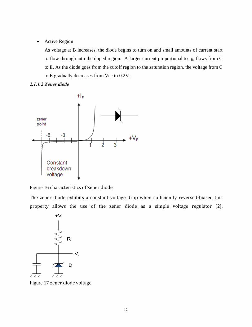
2.1.1.2 Zener diode
Figure 16 characteristics of Zener diode
The zener diode exhibits a constant voltage drop when sufficiently reversed-biased this
property allows the use of the zener diode as a simple voltage regulator [2].
Figure 17 zener diode voltage

16
Here, Vr will be equal to the reverse breakdown voltage of the zener diode and should be
constant. What is the purpose of the resistor in this circuit? Its job is to limit the current
flowing through the zener diode:
�= �����
(2.1)
2.1.1.3 Working principle of a voltage regulator
Figure 13 shows a simple voltage regulator circuit that employs an operational amplifier (op-
amp). As its name implies, this circuit accepts an unregulated voltage input (that is, a
fluctuating input voltage), and provides a regulated voltage output (that is, a stable output
voltage that remains at or very close to its intended output level).
The zener diode Vz acts as a voltage reference for the circuit, and is fed into the non-inverting
input of the operational amplifier. The voltage divider formed by R1 and R2 sets the voltage
level of the inverting input of the op amp, which is basically a feedback from the circuit
output to the op amp. The NPN transistor is used to boost the output current of the circuit.
The voltage at the non-inverting input of the op amp is pegged at the zener voltage, while the
voltage at the inverting input is always a fraction of the output voltage as defined by R2 and
R1. When the output exceeds the set level, the inverting input voltage exceeds that of the
non-inverting input, causing the output of the op-amp to go 'low'. This turns off the NPN
transistor, causing the output voltage to dip. When the output goes below the set level, the
reverse happens, that is, the op-amp output goes 'high', causing the NPN transistor to turn on
and pull the voltage up.
Thus, this circuit works by turning off the transistor when the output voltage is too high and
turning it on when the output is too low. This balancing act happens continuously, with the
circuit reacting instantaneously to deviations in the output voltage. Resistor R2 is adjusted to
set the desired output voltage of the circuit
2.1.1.4 Measures of regulator quality
The output voltage can only be held roughly constant; the regulation may be specified by the
following measurements:

17
• Load regulation is the change in output voltage for a given change in load current
(for example: "typically 15mV, maximum 100mV for load currents between 5mA and
1.4A, at some specified temperature and input voltage").
• line regulation or input regulation is the degree to which output voltage changes
with input (supply) voltage changes - as a ratio of output to input change (for example
"typically 13mV/V"), or the output voltage change over the entire specified input voltage
range
• Initial accuracy of a voltage regulator (or simply "the voltage accuracy") reflects
the error in output voltage for a fixed regulator without taking into account temperature
or aging effects on output accuracy.
• Dropout voltage is the minimum difference between input voltage and output
voltage for which the regulator can still supply the specified current. A Low Drop-Out
(LDO) regulator is designed to work well even with an input supply only a Volt or so
above the output voltage.
Referring Fig.2.1 then it follows that,
��′ = ��{��− ��� �������
�} (2.2)
��� = ���+ �� (2.3)
���+ �� = ��{��− ��� �������
�} (2.4)
���1 + ��� �������
��= ���+ ���� (2.5)
�� = ��������
����� ��������
(2.6)
�� =������
���
���� ��������
(2.7)
Now, since Ad>>1, then Vo becomes approximately;
Vo ≈ Vz ��������
� (2.8)
Using the values given,
Vz=6.2V, R1=R2=10kΩ
Then we have Vo as
Vo ≈ 6.2 �����������
�≈ 12.4V (2.9)

18
2.1.2 The Comparator stage
Practical operational amplifier voltage gains are in the range of 200,000 or more, which makes
them almost useless as an analog differential amplifier by themselves. For an op-amp with a
voltage gain (AV) of 200,000 and a maximum output voltage swing of +15V/-15V, all
it would take is a differential input voltage of 75 µV (microvolts) to drive it to saturation or
cutoff.
One application of the op-amp is the comparator. The output of an op-amp will be saturated fully
positive if the (+) input is more positive than the (-) input, and saturated fully negative if the (+)
input is less positive than the (-) input. In other words, an op-amp's extremely high voltage gain
makes it useful as a device to compare two voltages and change output voltage states when one
input exceeds the other in magnitude.
A comparator is a circuit that compares two input voltages and produces an output in either of
two states, indicating the greater than or less than relationship of the inputs. A comparator
switches to one state when the input reaches the upper trigger point. It switches back to the other
state when the input falls below the lower trigger point. The comparator compares a reference
voltage, fixed or variable, with an input waveform. If the input is applied to the non-inverting
input and the reference to the inverting input, the comparator will be operating in the non-
inverting mode. In this case, when the input voltage is equal to (or slightly less than) the
reference voltage the output will be at its lowest limit (near the negative supply) and when the
input is equal to (or slightly greater than) the reference voltage the output will change to its
highest value (near the positive supply). If the inverting and non-inverting terminals are reversed
the comparator will operate in the inverting mode [3].
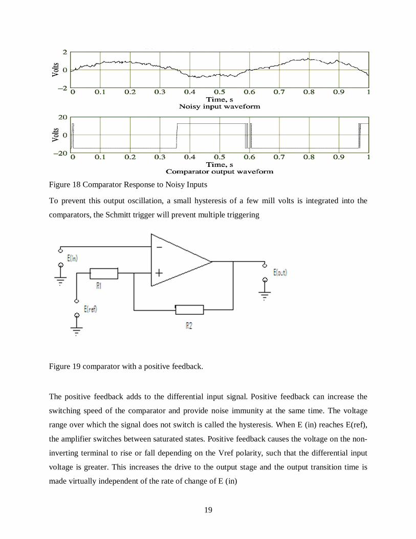
2.1.2.1 Hysteresis
A comparator normally changes its output state when the voltage between its inputs crosses
through approximately zero volts. Small voltage fluctuations due to noise, always present on the
inputs can cause undesirable rapid changes between the two output states when the input voltage
difference is near zero volts [1].
19
Figure 18 Comparator Response to Noisy Inputs
To prevent this output oscillation, a small hysteresis of a few mill volts is integrated into the
comparators, the Schmitt trigger will prevent multiple triggering
Figure 19 comparator with a positive feedback.
The positive feedback adds to the differential input signal. Positive feedback can increase the
switching speed of the comparator and provide noise immunity at the same time. The voltage
range over which the signal does not switch is called the hysteresis. When E (in) reaches E(ref),
the amplifier switches between saturated states. Positive feedback causes the voltage on the non-
inverting terminal to rise or fall depending on the Vref polarity, such that the differential input
voltage is greater. This increases the drive to the output stage and the output transition time is
made virtually independent of the rate of change of E (in)

20
In hysteresis transition takes place for different values of E (in) depending on whether the E (in)
is increasing or decreasing towards the threshold value.
The threshold value for E (in) at which the transition takes place has a value, neglecting offsets,
equal to:
�o(sat) ��(�����) (2.10)
The value of hysteresis is therefore,
VH = (Vo+ (sat)-VO-(sat)) ��
(�����) (2.11)
The amount of hysteresis is directly dependent on magnitude of the positive feedback fraction:
β = ��(�����) (2.12)
using R1=47Ω, R2=10kΩ, then,
VH = �12 − 0� ��������
= 0.0561V = 56mV (2.12a)
Small β results in high frequency oscillations at switching and hence should be avoided.
In place of one switching point, hysteresis introduces two: one for rising voltages, and one for
falling voltages. The difference between the higher-level trip value (VTRIP+) and the lower-level
trip value (VTRIP-) equals the hysteresis voltage (VHYST).
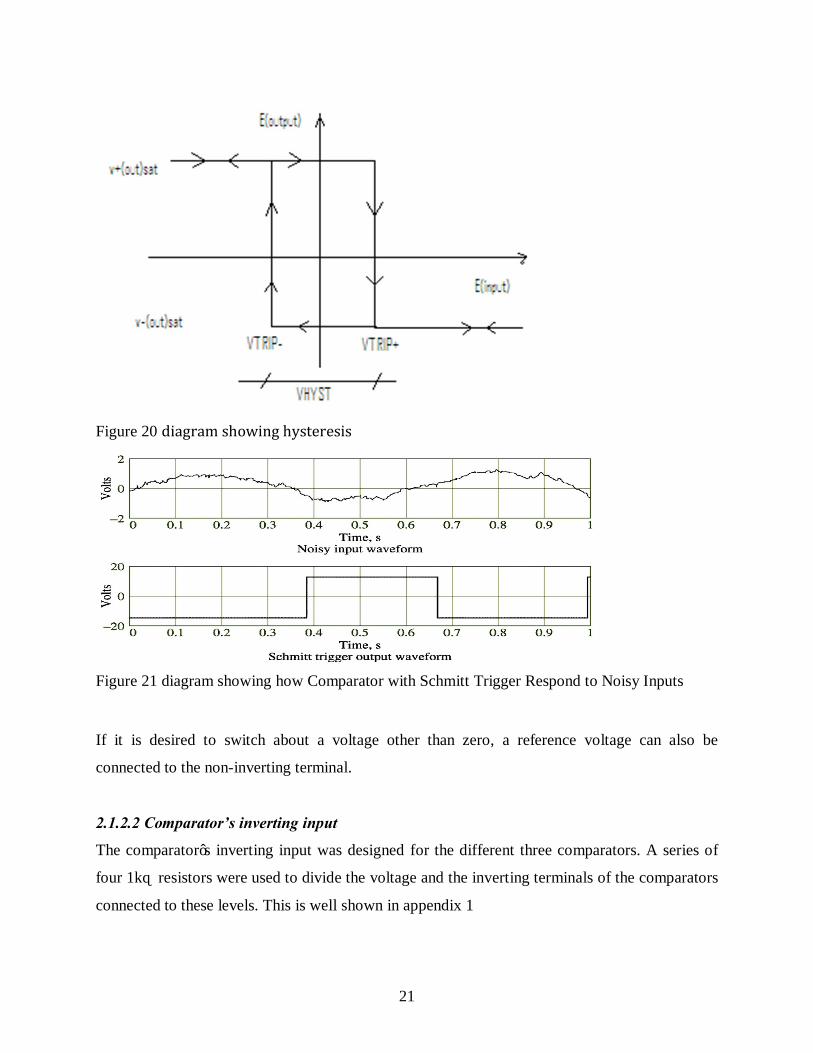
21
Figure 20 diagram showing hysteresis
Figure 21 diagram showing how Comparator with Schmitt Trigger Respond to Noisy Inputs
If it is desired to switch about a voltage other than zero, a reference voltage can also be
connected to the non-inverting terminal.
2.1.2.2 Comparator’s inverting input
The comparator’s inverting input was designed for the different three comparators. A series of
four 1kΩ resistors were used to divide the voltage and the inverting terminals of the comparators
connected to these levels. This is well shown in appendix 1
22
2.1.2.3 Comparator’s non-inverting input
A 100Ω resistor in series with a 5kΩ potentiometer was used at the non-inverting input. The
input thus varied using the potentiometer.
2.1.3 The output stage
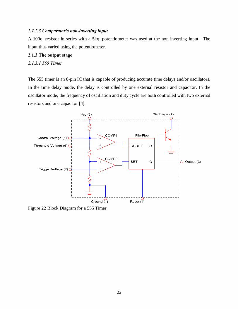
2.1.3.1 555 Timer
The 555 timer is an 8-pin IC that is capable of producing accurate time delays and/or oscillators.
In the time delay mode, the delay is controlled by one external resistor and capacitor. In the
oscillator mode, the frequency of oscillation and duty cycle are both controlled with two external
resistors and one capacitor [4].
Figure 22 Block Diagram for a 555 Timer

23
Figure 23 Schematic of a 555 Timer in Oscillator Mode
555 Timer design equations
Figure 24 tHIGH : Calculations for the Oscillator’s HIGH Time
�������� 0.693��� � ��� (2.13)
The Output Is HIGH While Charging The Capacitor Is through

24
Figure 25 tLOW : Calculations for the Oscillator’s LOW Time
����� �� 0.693RBC (2.14)
PERIOD;
� � �������� ������ (2.15)
� � �0.693��� � ������ �0.693���� (2.16)
� � 0.693��� � ���� (2.17)
DUTY CYCLE:
�� � ��������
∗ 100% (2.18)
DC � �.������������.������������
∗ 100% (2.19)
�� � �����������������
∗ 100% (2.20)
The Output Is LOW While The Capacitor Is Discharging Through RB.
25
FREQUENCY;
� � �� (2.21)
� � ��.������������
(2.22)
Given that audio frequency ranges from 20Hz to 20 kHz, designing for audio frequency output
using RA=RB=1kΩ, C1=0.1µF, C2=0.01µF
Then,
� � ��.������������������.�∗���� � 4.810��� (3.23)
This is within the audio frequency 20�� � � � 20���
The timer voltage input (vcc) was triggered using a transistor as the third comparator’s output
went high. The transistor’s base was connected to the comparator’s output . A 1kΩ resistor was
used to limit the transistor’s base current.
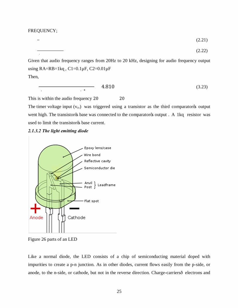
2.1.3.2 The light emitting diode
Figure 26 parts of an LED
Like a normal diode, the LED consists of a chip of semiconducting material doped with
impurities to create a p-n junction. As in other diodes, current flows easily from the p-side, or
anode, to the n-side, or cathode, but not in the reverse direction. Charge-carriers—electrons and

26
holes—flow into the junction from electrodes with different voltages. When an electron meets a
hole, it falls into a lower energy level, and releases energy in the form of a photon The
wavelength of the light emitted, and thus its color depends on the band gap energy of the
materials forming the p-n junction. In silicon or germanium diodes, the electrons and holes
recombine by a non-radiative transition which produces no optical emission, because these are
indirect band gap materials. The materials used for the LED have a direct band gap with energies
corresponding to near-infrared, visible or near-ultraviolet light.
Figure 27 I-V characteristics for a diode.
An LED will begin to emit light when the on-voltage is exceeded. Typical on voltages are 2–3
volts. The LED used will have a voltage drop, specified at the intended operating current. Ohm's
law and Kirchhoff's circuit laws are used to calculate the resistor that is used to attain the correct
current. The resistor value is computed by subtracting the LED voltage drop from the supply
voltage, and then dividing by the desired LED operating current. If the supply voltage is equal to
the LED's voltage drop, no resistor is needed. The formula to calculate the correct resistance to
use is:
��������������� �� ��� ����������������������� ������������������ �����������������
(2.23)
27
Where:
• Power supply voltage (Vs) is the voltage of the power supply e.g. a 9 volt battery.
• LED voltage drop (Vf) is the voltage drop across the LED (typically about 1.8 - 3.3 volts;
this varies by the color of the LED) 1.8 volts for red and its gets higher as the spectrum
increases to 3.3 volts for blue.
• LED current rating (If) is the manufacturer rating of the LED (usually given in mill
amperes such as 20 mA)
Analysis using Kirchhoff's Laws; The formula can be explained considering the LED as a ����
Ω
resistance, and applying the KVL (R is the unknown quantity):
�� = ��+ �� = ���+ ����
�� (2.24)
� = �������
(2.25).
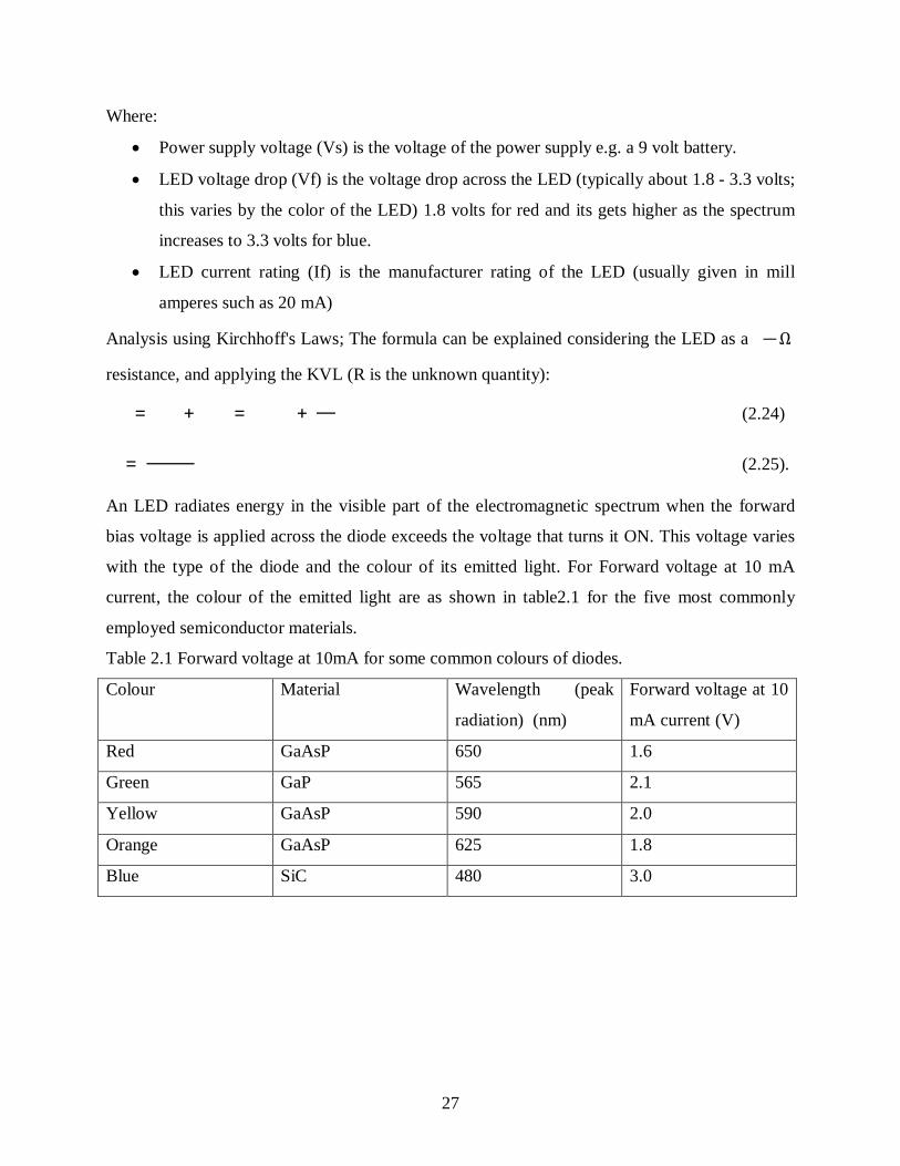
An LED radiates energy in the visible part of the electromagnetic spectrum when the forward
bias voltage is applied across the diode exceeds the voltage that turns it ON. This voltage varies
with the type of the diode and the colour of its emitted light. For Forward voltage at 10 mA
current, the colour of the emitted light are as shown in table2.1 for the five most commonly
employed semiconductor materials.
Table 2.1 Forward voltage at 10mA for some common colours of diodes.
Colour Material Wavelength (peak
radiation) (nm)
Forward voltage at 10
mA current (V)
Red GaAsP 650 1.6
Green GaP 565 2.1
Yellow GaAsP 590 2.0
Orange GaAsP 625 1.8
Blue SiC 480 3.0

28
CHAPTER 3
3.1DESIGN RESULTS
The following results were obtained from the implemented circuit:
3.1.1 Voltage regulator results:
Table 3.1; voltage regulator results.
Input voltage (V) Output voltage (V)
(without load)
Output voltage (V)
(with load)
11.7 10.3 9.9
12,0 10.7 10.2
14.0 12.5 12.0
3.1.2 Comparator and output stages’ results
The results were obtained for a constant input voltage (Vcc) set at 12 V. The comparators
U2A,U1A and U3A shown in APPENDIX 1 had the following results. It is noted that the non
inverting input was adjusted using the potentiometer until all the LEDs lit then the tabulation in
table 3.2 was made.
Table 3.2: comparator and output stage’s results
Comparator Inverting input (V) Output voltage (V) observation
U2A 3.13 7.58 Green LED lit
U1A 6.26 7.03 Yellow LED lit
U3A 9.43 8.94 Red LED lit and buzzer ON
The transistor Q1 base was biased when comparator U3A had a HIGH output and it acted as a
switch for the timer to be at Vcc.

29
CHAPTER 4
5.1 CONCLUSION
The objective of the project was achieved where implementation of the brake deterioration
indicator was done. The implementation was achieved using locally available components hence
making it easier to build. With guidance from the Supervisor, the concept was conceptualized
and developed to a desirable achievement. The voltage regulator was used to ensure that the level
of voltage that was fed into the comparator stage and the output stage especially the 555 timer
part was within the design levels. The use of comparators, 555 timer, transistor and op amp as
learnt during the course as among other electronics based lessons were practically exploited.
5.2 RECOMMENDATIONS
• For interfacing of the circuitry with the vehicles brake system, an appropriate
method to transduce the brake pedal travel into electric signal should be designed.
This should be done via a push button that would enable the driver to engage or
disengage the circuitry from its functions, a condition that is necessary especially
when the brakes have deteriorated. When the system notifies the driver that the
brakes have failed, he may disengage the indicator from power so as to eliminate
the buzzing sound that would otherwise be a nuisance to the people on board.
• The zener diode in the voltage regulator needs to be replaced by a voltage
reference IC for a more stable and more precise output voltage.

30
APPENDIX A Design simulation for the voltage regulator.
V19 V
R110kΩ
R21kΩ
D1ZPD6.2
Q1BC108BP
R310kΩ
XMM1
03
4
U1
UA741CD
3
2
4
7
6
5 15 2
1
0

31
APPENDIX B Design simulation showing the comparator and the output parts
V112 V
R11kΩ
R2
1kΩR41kΩ
R51kΩ
R61kΩ
R7100Ω
R85kΩKey=A 95%
R14
330Ω
R15
330Ω
XMM1
R3
47Ω
R9
47Ω
R10
47Ω
R11
10kΩ
7
R12
10kΩ
R13
10kΩ
0
U1A
TL084ACN
3
2 11
4
1
U3A
TL084CN
3
2
11
4
1
U2A
TL084CN
3
2
11
4
1
1
8
3
4
2
LED2
0
LED4
LED1
C2
10nF
R161kΩ
R171kΩ
C1
100nF
U4
SONALERT200 Hz
Q1BC108BP
A1
555_VIRTUALGND
DISOUTRST
VCC
THR
CONTRI
19
16
18
09
5
10
0
15
0
0
14
11
17
6
22
R18
1kΩ
13
210
20

32
REFFERENCES
[1.] http://www.allaboutcircuits.com
[2.] Owen Bishop, Electronic circuits & systems, @2007, published by Elsevier ltd
[3.] George Clayton &Steve Winder, Operational Amplifiers, 4th Edition, @2000
[4.] Paul m. Chirlian, Analysis and design of integrated Electronic circuits,@1981