BQ40Z50-R2 1-Series, 2-Series, 3-Series, and 4-Series Li ...
55
BQ40Z50-R2 1-Series, 2-Series, 3-Series, and 4-Series Li-Ion Battery Pack Manager 1 Features • Fully integrated 1-series, 2-series, 3-series, and 4-series Li-ion or Li-polymer cell battery pack manager and protection • Next-generation patented Impedance Track ™ technology accurately measures available charge in Li-ion and Li-polymer batteries • High-side N-CH protection FET drive • Integrated cell balancing while charging or at rest • Suitable for batteries between 100 mAh and 29 Ah • Full array of programmable protection features – Voltage – Current – Temperature – Charge timeout – CHG/DSG FETs – AFE • Sophisticated charge algorithms – JEITA – Enhanced charging – Adaptive charging – Cell balancing • Supports TURBO Mode 2.0 • Supports battery trip point (BTP) • Diagnostic lifetime data monitor and black box recorder • LED display • Supports two-wire SMBus v1.1 interface • SHA-1 authentication • IATA support • Compact package: 32-lead QFN (RSM) 2 Applications • Tablets • Drones • UPS/battery backup systems • Medical equipment • Handheld vacuum cleaners and vacuum robots 3 Description The BQ40Z50-R2 device, incorporating patented Impedance Track ™ technology, is a fully integrated, single-chip, pack-based solution that provides a rich array of features for gas gauging, protection, and authentication for 1-series, 2-series, 3-series, and 4- series cell Li-ion and Li-polymer battery packs. Using its integrated high-performance analog peripherals, the BQ40Z50-R2 device measures and maintains an accurate record of available capacity, voltage, current, temperature, and other critical parameters in Li-ion or Li-polymer batteries, and reports this information to the system host controller over an SMBus v1.1 compatible interface. Device Information PART NUMBER PACKAGE BODY SIZE (NOM) BQ40Z50-R2 VQFN (32) 4.00 mm × 4.00 mm CHG DSG BAT PACK VCC VC4 VC3 VC2 VC1 VSS SRN SRP PACK+ PACK– PRES SMBC SMBD SMBD SMBC PBI TS1 TS2 FUSE LEDCNTLA LEDCNTLB DISP PTC LEDCNTLC TS3 TS4 BTP BTP VC1 VC2 VC3 OUT VDD GND 2 nd level protector Cell 1 Cell 2 Cell 3 PRES PCHG Copyright © 2017, Texas Instruments Incorporated Simplified Schematic www.ti.com BQ40Z50-R2 SLUSCS4C – JUNE 2017 – REVISED APRIL 2021 Copyright © 2021 Texas Instruments Incorporated Submit Document Feedback 1 Product Folder Links: BQ40Z50-R2 BQ40Z50-R2 SLUSCS4C – JUNE 2017 – REVISED APRIL 2021 An IMPORTANT NOTICE at the end of this data sheet addresses availability, warranty, changes, use in safety-critical applications, intellectual property matters and other important disclaimers. PRODUCTION DATA.
Transcript of BQ40Z50-R2 1-Series, 2-Series, 3-Series, and 4-Series Li ...

BQ40Z50-R2 1-Series, 2-Series, 3-Series, and 4-Series Li-Ion Battery Pack Manager
1 Features• Fully integrated 1-series, 2-series, 3-series, and
4-series Li-ion or Li-polymer cell battery packmanager and protection
• Next-generation patented Impedance Track™
technology accurately measures available chargein Li-ion and Li-polymer batteries
• High-side N-CH protection FET drive• Integrated cell balancing while charging or at rest• Suitable for batteries between 100 mAh and 29 Ah• Full array of programmable protection features
– Voltage– Current– Temperature– Charge timeout– CHG/DSG FETs– AFE
• Sophisticated charge algorithms– JEITA– Enhanced charging– Adaptive charging– Cell balancing
• Supports TURBO Mode 2.0• Supports battery trip point (BTP)• Diagnostic lifetime data monitor and black box
recorder• LED display• Supports two-wire SMBus v1.1 interface• SHA-1 authentication• IATA support• Compact package: 32-lead QFN (RSM)
2 Applications• Tablets• Drones• UPS/battery backup systems• Medical equipment• Handheld vacuum cleaners and vacuum robots
3 DescriptionThe BQ40Z50-R2 device, incorporating patentedImpedance Track™ technology, is a fully integrated,single-chip, pack-based solution that provides a richarray of features for gas gauging, protection, andauthentication for 1-series, 2-series, 3-series, and 4-series cell Li-ion and Li-polymer battery packs.
Using its integrated high-performance analogperipherals, the BQ40Z50-R2 device measures andmaintains an accurate record of available capacity,voltage, current, temperature, and other criticalparameters in Li-ion or Li-polymer batteries, andreports this information to the system host controllerover an SMBus v1.1 compatible interface.
Device InformationPART NUMBER PACKAGE BODY SIZE (NOM)
BQ40Z50-R2 VQFN (32) 4.00 mm × 4.00 mm
CH
G
DS
G
BAT
PA
CK
VC
C
VC4
VC3
VC2
VC1
VSS SRNSRP
PACK+
PACK–
PRES
SMBC
SMBDSMBD
SMBCPBI
TS1 TS2
FU
SE LEDCNTLA
LEDCNTLB
DISP
PT
C
LEDCNTLC
TS3 TS4 BTP
BTP
VC1
VC2
VC3OUT
VDD
GND
2n
dle
ve
l
pro
tec
tor
Cell 1
Cell 2
Cell 3
PRES
PC
HG
Copyright © 2017, Texas Instruments Incorporated
Simplified Schematic
www.ti.comBQ40Z50-R2
SLUSCS4C – JUNE 2017 – REVISED APRIL 2021
Copyright © 2021 Texas Instruments Incorporated Submit Document Feedback 1
Product Folder Links: BQ40Z50-R2
BQ40Z50-R2SLUSCS4C – JUNE 2017 – REVISED APRIL 2021
An IMPORTANT NOTICE at the end of this data sheet addresses availability, warranty, changes, use in safety-critical applications,intellectual property matters and other important disclaimers. PRODUCTION DATA.
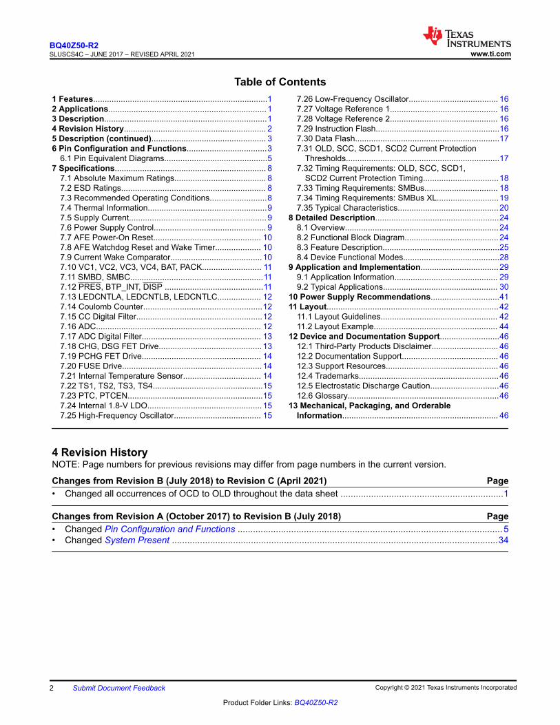
Table of Contents1 Features............................................................................12 Applications..................................................................... 13 Description.......................................................................14 Revision History.............................................................. 25 Description (continued).................................................. 36 Pin Configuration and Functions...................................3
6.1 Pin Equivalent Diagrams.............................................57 Specifications.................................................................. 8
7.1 Absolute Maximum Ratings........................................ 87.2 ESD Ratings............................................................... 87.3 Recommended Operating Conditions.........................87.4 Thermal Information....................................................97.5 Supply Current............................................................ 97.6 Power Supply Control................................................. 97.7 AFE Power-On Reset............................................... 107.8 AFE Watchdog Reset and Wake Timer.................... 107.9 Current Wake Comparator........................................107.10 VC1, VC2, VC3, VC4, BAT, PACK.......................... 117.11 SMBD, SMBC..........................................................117.12 PRES, BTP_INT, DISP ...........................................117.13 LEDCNTLA, LEDCNTLB, LEDCNTLC................... 127.14 Coulomb Counter....................................................127.15 CC Digital Filter.......................................................127.16 ADC........................................................................ 127.17 ADC Digital Filter.................................................... 137.18 CHG, DSG FET Drive............................................. 137.19 PCHG FET Drive.................................................... 147.20 FUSE Drive............................................................. 147.21 Internal Temperature Sensor.................................. 147.22 TS1, TS2, TS3, TS4................................................157.23 PTC, PTCEN...........................................................157.24 Internal 1.8-V LDO.................................................. 157.25 High-Frequency Oscillator...................................... 15
7.26 Low-Frequency Oscillator....................................... 167.27 Voltage Reference 1............................................... 167.28 Voltage Reference 2............................................... 167.29 Instruction Flash......................................................167.30 Data Flash...............................................................177.31 OLD, SCC, SCD1, SCD2 Current Protection
Thresholds...................................................................177.32 Timing Requirements: OLD, SCC, SCD1,
SCD2 Current Protection Timing.................................187.33 Timing Requirements: SMBus................................ 187.34 Timing Requirements: SMBus XL...........................197.35 Typical Characteristics............................................ 20
8 Detailed Description......................................................248.1 Overview................................................................... 248.2 Functional Block Diagram......................................... 248.3 Feature Description...................................................258.4 Device Functional Modes..........................................28
9 Application and Implementation.................................. 299.1 Application Information............................................. 299.2 Typical Applications.................................................. 30
10 Power Supply Recommendations..............................4111 Layout...........................................................................42
11.1 Layout Guidelines................................................... 4211.2 Layout Example...................................................... 44
12 Device and Documentation Support..........................4612.1 Third-Party Products Disclaimer............................. 4612.2 Documentation Support.......................................... 4612.3 Support Resources................................................. 4612.4 Trademarks.............................................................4612.5 Electrostatic Discharge Caution..............................4612.6 Glossary..................................................................46
13 Mechanical, Packaging, and OrderableInformation.................................................................... 46
4 Revision HistoryNOTE: Page numbers for previous revisions may differ from page numbers in the current version.
Changes from Revision B (July 2018) to Revision C (April 2021) Page• Changed all occurrences of OCD to OLD throughout the data sheet ................................................................1
Changes from Revision A (October 2017) to Revision B (July 2018) Page• Changed Pin Configuration and Functions ........................................................................................................ 5• Changed System Present ................................................................................................................................34
BQ40Z50-R2SLUSCS4C – JUNE 2017 – REVISED APRIL 2021 www.ti.com
2 Submit Document Feedback Copyright © 2021 Texas Instruments Incorporated
Product Folder Links: BQ40Z50-R2

5 Description (continued)The BQ40Z50-R2 device supports TURBO Mode 2.0 by providing the available max power and max current tothe host system. The device also supports Battery Trip Point to send a BTP interrupt signal to the host system atthe preset state of charge thresholds.
The BQ40Z50-R2 provides software-based 1st- and 2nd-level safety protection against overvoltage,undervoltage, overcurrent, short-circuit current, overload, and overtemperature conditions, as well as other pack-and cell-related faults.
SHA-1 authentication, with secure memory for authentication keys, enables identification of genuine batterypacks.
The compact 32-lead QFN package minimizes solution cost and size for smart batteries while providingmaximum functionality and safety for battery gauging applications.
6 Pin Configuration and Functions3
2B
AT
9V
SS
1PBI 24 PTCEN
31
CH
G1
0T
S1
2VC4 23 PTC
30
PC
HG
11
TS
2
3VC3 22 LEDCNTLC
29
NC
12
TS
3
4VC2 21 LEDCNTLB
28
DS
G1
3T
S4
5VC1 20 LEDCNTLA
27
PA
CK
14
NC
6SRN 19 SMBC
26
VC
C1
5B
TP
_IN
T
7NC 18 SMBD
25
FU
SE
16
PR
ES
or
SH
UT
DN
8SRP 17 DISP
Not to scale
Thermal
Pad
Table 6-1. Pin FunctionsPIN NUMBER PIN NAME TYPE DESCRIPTION
1 PBI P(1) Power supply backup input pin. Connect to the 2.2-µF capacitor to VSS.
2 VC4 IA
Sense voltage input pin for the most positive cell, and balance current inputfor the most positive cell. Should be connected to the positive terminal of thefourth cell from the bottom of the stack with a 100-Ω series resistor and a0.1-μF capacitor to VC3. If not used, connect to VC3.
3 VC3 IA
Sense voltage input pin for the third-most positive cell, balance current inputfor the third-most positive cell, and return balance current for the mostpositive cell. Should be connected to the positive terminal of the third cell fromthe bottom of the stack with a 100-Ω series resistor and a 0.1-μF capacitor toVC2. If not used, connect to VC2.
4 VC2 IA
Sense voltage input pin for the second-most positive cell, balance currentinput for the second-most positive cell, and return balance current for thethird-most positive cell. Should be connected to the positive terminal of thesecond cell from the bottom of the stack with a 100-Ω series resistor and a0.1-μF capacitor to VC1. If not used, connect to VC1.
5 VC1 IA
Sense voltage input pin for the least positive cell, balance current input forthe least positive cell, and return balance current for the second-most positivecell. Should be connected to the positive terminal of the first cell from thebottom of the stack with a 100-Ω series resistor and a 0.1-μF capacitor toVSS.
www.ti.comBQ40Z50-R2
SLUSCS4C – JUNE 2017 – REVISED APRIL 2021
Copyright © 2021 Texas Instruments Incorporated Submit Document Feedback 3
Product Folder Links: BQ40Z50-R2

Table 6-1. Pin Functions (continued)PIN NUMBER PIN NAME TYPE DESCRIPTION
6 SRN IAnalog input pin connected to the internal coulomb counter peripheral forintegrating a small voltage between SRP and SRN where SRP is the top ofthe sense resistor.
7 NC — Not internally connected. It is okay to leave floating or to tie to VSS.
8 SRP IAnalog input pin connected to the internal coulomb counter peripheral forintegrating a small voltage between SRP and SRN where SRP is the top ofthe sense resistor.
9 VSS P Device ground
10 TS1 IA Temperature sensor 1 thermistor input pin. Connect to thermistor-1. If notused, connect directly to VSS and configure data flash accordingly.
11 TS2 IA Temperature sensor 2 thermistor input pin. Connect to thermistor-2. If notused, connect directly to VSS and configure data flash accordingly.
12 TS3 IA Temperature sensor 3 thermistor input pin. Connect to thermistor-3. If notused, connect directly to VSS and configure data flash accordingly.
13 TS4 IA Temperature sensor 4 thermistor input pin. Connect to thermistor-4. If notused, connect directly to VSS and configure data flash accordingly.
14 NC — Not internally connected. It is okay to leave floating or to tie to VSS.
15 BTP_INT O Battery Trip Point (BTP) interrupt output. If not used, connect directly to VSS.
16 PRES or SHUTDN IHost system present input for removable battery pack or emergency systemshutdown input for embedded pack. A pullup is not required for this pin. If notused, connect directly to VSS.
17 DISP — Display control for LEDs. If not used, connect directly to VSS.
18 SMBD I/OD SMBus data pin
19 SMBC I/OD SMBus clock pin
20 LEDCNTLA —LED display segment that drives the external LEDs depending on thefirmware configuration. If LEDs are not used, these pins can be left floating orconnected to VSS through a 20-kΩ resistor.
21 LEDCNTLB —LED display segment that drives the external LEDs depending on thefirmware configuration. If LEDs are not used, these pins can be left floating orconnected to VSS through a 20-kΩ resistor.
22 LEDCNTLC —LED display segment that drives the external LEDs depending on thefirmware configuration. If LEDs are not used, these pins can be left floating orconnected to VSS through a 20-kΩ resistor.
23 PTC IA Safety PTC thermistor input pin. To disable, connect both PTC and PTCEN toVSS.
24 PTCEN IA Safety PTC thermistor enable input pin. Connect to BAT. To disable, connectboth PTC and PTCEN to VSS.
25 FUSE O Fuse drive output pin. If not used, connect directly to VSS.
26 VCC P Secondary power supply input
27 PACK IA Pack sense input pin
28 DSG O NMOS Discharge FET drive output pin. If not used, it can be left floating orconnected to VSS through a 20-kΩ resistor.
29 NC — Not internally connected. It is okay to leave floating or to tie to VSS.
30 PCHG O PMOS Precharge FET drive output pin. If not used, it can be left floating orconnected to VSS through a 20-kΩ resistor.
31 CHG O NMOS Charge FET drive output pin. If not used, it can be left floating orconnected to VSS through a 20-kΩ resistor.
32 BAT P Primary power supply input pin
(1) P = Power Connection, O = Digital Output, AI = Analog Input, I = Digital Input, I/OD = Digital Input/Output
BQ40Z50-R2SLUSCS4C – JUNE 2017 – REVISED APRIL 2021 www.ti.com
4 Submit Document Feedback Copyright © 2021 Texas Instruments Incorporated
Product Folder Links: BQ40Z50-R2

6.1 Pin Equivalent Diagrams
BAT PACKVCC
PBIReference
System1.8 V
Domain
+
– PACK
Detector
BATDET
ENVCC3.1 V
Shutdown
Latch
BAT
Control
ENBAT
PACKDET
SHUTDOWN
SHOUT
BATCHG
Pump
CHG2 kΩ
CHGOFF
CHGEN
BATDSG
Pump
DSG2 kΩ
DSGEN
PACK
DSGOFF
Power Supply Control
CHG, DSG Drive
PCHG2 kΩ
VCC
PCHGEN
8 kΩ
Pre-Charge Drive
VCC
Zero-Volt Charge
BATCHG
Pump
CHGEN
BATZVCD
ZVCHGEN
Cell Balancing
VC1
VC2
VC3
VC4
CDEN4
CDEN3
CDEN2
CDEN1
ADC Mux ADC
Figure 6-1. Pin Equivalent Diagram 1
www.ti.comBQ40Z50-R2
SLUSCS4C – JUNE 2017 – REVISED APRIL 2021
Copyright © 2021 Texas Instruments Incorporated Submit Document Feedback 5
Product Folder Links: BQ40Z50-R2

SMBus Interface
100 kΩ
1 MΩ
SMBCSMBCIN
SMBCENSMBCOUT
100 kΩ
1 MΩ
SMBDSMBDIN
SMBDENSMBDOUT
FUSE
2 kΩ
FUSE Drive
FUSEEN
BATFUSEWKPUP
100 kΩ FUSEDIG
150 nA
Thermistor Inputs
ADTHx
2 kΩ
TS1,2,3,4
18 kΩ
1.8 V
ADC Mux
High-Voltage GPIO
RHOEN
PBI
100 kΩ
RHIN
10 kΩ
PRES
RHOUT
LED Drive
RLOEN
BAT
100 kΩ
RLIN
LED1, 2, 3
RLOUT
22.5 mA
ADC
RCWKPUP
1 kΩ RCIN
RCOUT
1.8 V
RCPUP
1.8 V
Figure 6-2. Pin Equivalent Diagram 2
BQ40Z50-R2SLUSCS4C – JUNE 2017 – REVISED APRIL 2021 www.ti.com
6 Submit Document Feedback Copyright © 2021 Texas Instruments Incorporated
Product Folder Links: BQ40Z50-R2

VC and PACK Dividers
CHANx
1.9 MΩ
VC4
0.1 MΩ
10 Ω
ADC Mux ADC
CHANx
1.9 MΩ
PACK
0.1 MΩ
10 Ω
ADC Mux ADC
OLD , SCC, SCD Comparators and Coulomb Counter
SRP
SRN
3.8 kΩ
3.8 kΩ
Comparator
Array
100 Ω
100 Ω
Coulomb
Counter
Φ2
Φ1
Φ2
Φ1
Φ2
Φ1
Φ2
Φ1
4
Figure 6-3. Pin Equivalent Diagram 3
www.ti.comBQ40Z50-R2
SLUSCS4C – JUNE 2017 – REVISED APRIL 2021
Copyright © 2021 Texas Instruments Incorporated Submit Document Feedback 7
Product Folder Links: BQ40Z50-R2

7 Specifications7.1 Absolute Maximum RatingsOver-operating free-air temperature range (unless otherwise noted)(1)
MIN MAX UNITSupply voltage range,VCC
BAT, VCC, PBI –0.3 30 V
Input voltage range, VIN
PACK, SMBC, SMBD, PRES or SHUTDN, BTP_INT, DISP –0.3 30 V
TS1, TS2, TS3, TS4 –0.3 VREG + 0.3 V
PTC, PTCEN, LEDCNTLA, LEDCNTLB, LEDCNTLC –0.3 VBAT + 0.3 V
SRP, SRN –0.3 0.3 V
VC4 VC3 – 0.3 VC3 + 8.5, orVSS + 30 V
VC3 VC2 – 0.3 VC2 + 8.5, orVSS + 30 V
VC2 VC1 – 0.3 VC1 + 8.5, orVSS + 30 V
VC1 VSS – 0.3 VSS + 8.5, orVSS + 30 V
Output voltage range,VO
CHG, DSG –0.3 32
PCHG, FUSE –0.3 30 V
Maximum VSS current, ISS 50 mA
Storage temperature, TSTG –65 150 °C
Lead temperature (soldering, 10 s), TSOLDER 300 °C
(1) Stresses beyond those listed under absolute maximum ratings may cause permanent damage to the device. These are stress ratingsonly, and functional operation of the device at these or any other conditions beyond those indicated under recommended operatingconditions is not implied. Exposure to absolute–maximum–rated conditions for extended periods may affect device reliability.
7.2 ESD RatingsVALUE UNIT
V(ESD)Electrostaticdischarge
Human-body model (HBM), per ANSI/ESDA/JEDEC JS-001(1) ±2000V
Charged-device model (CDM), per JEDEC specification JESD22-C101(2) ±500
(1) JEDEC document JEP155 states that 500-V HBM allows safe manufacturing with a standard ESD control process.(2) JEDEC document JEP157 states that 250-V CDM allows safe manufacturing with a standard ESD control process.
7.3 Recommended Operating ConditionsTypical values stated where TA = 25°C and VCC = 14.4 V, Min/Max values stated where TA = –40°C to 85°C and VCC =2.2 V to 26 V (unless otherwise noted)
MIN NOM MAX UNITVCC Supply voltage BAT, VCC, PBI 2.2 26 V
VSHUTDOWN– Shutdown voltage VPACK < VSHUTDOWN – 1.8 2.0 2.2 V
VSHUTDOWN+ Start-up voltage VPACK > VSHUTDOWN– + VHYS 2.05 2.25 2.45 V
VHYSShutdown voltagehysteresis VSHUTDOWN+ – VSHUTDOWN– 250 mV
BQ40Z50-R2SLUSCS4C – JUNE 2017 – REVISED APRIL 2021 www.ti.com
8 Submit Document Feedback Copyright © 2021 Texas Instruments Incorporated
Product Folder Links: BQ40Z50-R2

7.3 Recommended Operating Conditions (continued)Typical values stated where TA = 25°C and VCC = 14.4 V, Min/Max values stated where TA = –40°C to 85°C and VCC =2.2 V to 26 V (unless otherwise noted)
MIN NOM MAX UNIT
VIN Input voltage range
PACK, SMBC, SMBD, PRES, BTP_IN, DISP 26
V
TS1, TS2, TS3, TS4 VREG
PTC, PTCEN, LEDCNTLA, LEDCNTLB, LEDCNTLC VBAT
SRP, SRN –0.2 0.2
VC4 VVC3 VVC3 + 5
VC3 VVC2 VVC2 + 5
VC2 VVC1 VVC1 + 5
VC1 VVSS VVSS + 5
VOOutput voltagerange CHG, DSG, PCHG, FUSE 26 V
CPBIExternal PBIcapacitor 2.2 µF
TOPROperatingtemperature –40 85 °C
7.4 Thermal Information
THERMAL METRIC(1)
BQ40Z50-R2UNITRSM (QFN)
32 PINSRθJA, High K Junction-to-ambient thermal resistance 47.4 °C/W
RθJC(top) Junction-to-case(top) thermal resistance 40.3 °C/W
RθJB Junction-to-board thermal resistance 14.7 °C/W
ψJT Junction-to-top characterization parameter 0.8 °C/W
ψJB Junction-to-board characterization parameter 14.4 °C/W
RθJC(bottom) Junction-to-case(bottom) thermal resistance 3.8 °C/W
(1) For more information about traditional and new thermal metrics, see the Semiconductor and IC Package Thermal Metrics applicationreport, SPRA953.
7.5 Supply CurrentTypical values stated where TA = 25°C and VCC = 14.4 V, Min/Max values stated where TA = –40°C to 85°C and VCC =2.2 V to 20 V (unless otherwise noted)
PARAMETER TEST CONDITIONS MIN TYP MAX UNITINORMAL NORMAL mode CHG on. DSG on, no Flash write 336 µA
ISLEEP SLEEP modeCHG off, DSG on, no SBS communication 75
µACHG off, DSG off, no SBS communication 52
ISHUTDOWN SHUTDOWN mode 1.6 µA
7.6 Power Supply ControlTypical values stated where TA = 25°C and VCC = 14.4 V, Min/Max values stated where TA = –40°C to 85°C and VCC =2.2 V to 26 V (unless otherwise noted)
PARAMETER TEST CONDITIONS MIN TYP MAX UNIT
VSWITCHOVER–BAT to VCCswitchover voltage VBAT < VSWITCHOVER– 1.95 2.1 2.2 V
VSWITCHOVER+VCC to BATswitchover voltage VBAT > VSWITCHOVER– + VHYS 2.9 3.1 3.25 V
www.ti.comBQ40Z50-R2
SLUSCS4C – JUNE 2017 – REVISED APRIL 2021
Copyright © 2021 Texas Instruments Incorporated Submit Document Feedback 9
Product Folder Links: BQ40Z50-R2

7.6 Power Supply Control (continued)Typical values stated where TA = 25°C and VCC = 14.4 V, Min/Max values stated where TA = –40°C to 85°C and VCC =2.2 V to 26 V (unless otherwise noted)
PARAMETER TEST CONDITIONS MIN TYP MAX UNIT
VHYSSwitchovervoltage hysteresis VSWITCHOVER+ – VSWITCHOVER– 1000 mV
ILKGInput Leakagecurrent
BAT pin, BAT = 0 V, VCC = 25 V, PACK = 25 V 1
µAPACK pin, BAT = 25 V, VCC = 0 V, PACK = 0 V 1
BAT and PACK terminals, BAT = 0 V, VCC = 0 V, PACK =0 V, PBI = 25 V 1
7.7 AFE Power-On ResetTypical values stated where TA = 25°C and VCC = 14.4 V, Min/Max values stated where TA = –40°C to 85°C and VCC =2.2 V to 26 V (unless otherwise noted)
PARAMETER TEST CONDITIONS MIN TYP MAX UNIT
VREGIT–Negative-goingvoltage input VREG 1.51 1.55 1.59 V
VHYSPower-on resethysteresis VREGIT+ – VREGIT– 70 100 130 mV
tRSTPower-on resettime 200 300 400 µs
7.8 AFE Watchdog Reset and Wake TimerTypical values stated where TA = 25°C and VCC = 14.4 V, Min/Max values stated where TA = –40°C to 85°C and VCC =2.2 V to 26 V (unless otherwise noted)
PARAMETER TEST CONDITIONS MIN TYP MAX UNIT
tWDTAFE watchdogtimeout
tWDT = 500 372 500 628
mstWDT = 1000 744 1000 1256
tWDT = 2000 1488 2000 2512
tWDT = 4000 2976 4000 5024
tWAKE AFE wake timer
tWAKE = 250 186 250 314
mstWAKE = 500 372 500 628
tWAKE = 1000 744 1000 1256
tWAKE = 512 1488 2000 2512
tFETOFFFET off delay afterreset tFETOFF = 512 409 512 614 ms
7.9 Current Wake ComparatorTypical values stated where TA = 25°C and VCC = 14.4 V, Min/Max values stated where TA = –40°C to 85°C and VCC =2.2 V to 26 V (unless otherwise noted)PARAMETER TEST CONDITIONS MIN TYP MAX UNIT
VWAKEWake voltagethreshold
VWAKE = ±0.625 mV ±0.3 ±0.625 ±0.9
mVVWAKE = ±1.25 mV ±0.6 ±1.25 ±1.8
VWAKE = ±2.5 mV ±1.2 ±2.5 ±3.6
VWAKE = ±5 mV ±2.4 ±5.0 ±7.2
VWAKE(DRIFT)Temperature drift ofVWAKE accuracy 0.5% °C
tWAKE
Time fromapplication ofcurrent to wakeinterrupt
700 µs
BQ40Z50-R2SLUSCS4C – JUNE 2017 – REVISED APRIL 2021 www.ti.com
10 Submit Document Feedback Copyright © 2021 Texas Instruments Incorporated
Product Folder Links: BQ40Z50-R2

7.9 Current Wake Comparator (continued)Typical values stated where TA = 25°C and VCC = 14.4 V, Min/Max values stated where TA = –40°C to 85°C and VCC =2.2 V to 26 V (unless otherwise noted)PARAMETER TEST CONDITIONS MIN TYP MAX UNIT
tWAKE(SU)Wake comparatorstartup time 500 1000 µs
7.10 VC1, VC2, VC3, VC4, BAT, PACKTypical values stated where TA = 25°C and VCC = 14.4 V, Min/Max values stated where TA = –40°C to 85°C and VCC =2.2 V to 26 V (unless otherwise noted)
PARAMETER TEST CONDITIONS MIN TYP MAX UNIT
K Scaling factor
VC1–VSS, VC2–VC1, VC3–VC2, VC4–VC3 0.1980 0.2000 0.2020
—BAT–VSS, PACK–VSS 0.049 0.050 0.051
VREF2 0.490 0.500 0.510
VIN Input voltage rangeVC1–VSS, VC2–VC1, VC3–VC2, VC4–VC3 –0.2 5
VBAT–VSS, PACK–VSS –0.2 20
ILKG Input leakage current VC1, VC2, VC3, VC4, cell balancing off, cell detachdetection off, ADC multiplexer off 1 µA
RCBInternal cell balanceresistance RDS(ON) for internal FET switch at 2 V < VDS < 4 V 200 Ω
ICDInternal cell detachcheck current VCx > VSS + 0.8 V 30 50 70 µA
7.11 SMBD, SMBCTypical values stated where TA = 25°C and VCC = 14.4 V, Min/Max values stated where TA = –40°C to 85°C and VCC =2.2 V to 26 V (unless otherwise noted)
PARAMETER TEST CONDITIONS MIN TYP MAX UNITVIH Input voltage high SMBC, SMBD, VREG = 1.8 V 1.3 V
VIL Input voltage low SMBC, SMBD, VREG = 1.8 V 0.8 V
VOL Output low voltage SMBC, SMBD, VREG = 1.8 V, IOL = 1.5 mA 0.4 V
CIN Input capacitance 5 pF
ILKG Input leakage current 1 µA
RPD Pulldown resistance 0.7 1.0 1.3 MΩ
7.12 PRES, BTP_INT, DISPTypical values stated where TA = 25°C and VCC = 14.4 V, Min/Max values stated where TA = –40°C to 85°C and VCC =2.2 V to 26 V (unless otherwise noted)
PARAMETER TEST CONDITIONS MIN TYP MAX UNITVIH High-level input 1.3 V
VIL Low-level input 0.55 V
VOH Output voltage highVBAT > 5.5 V, IOH = –0 µA 3.5
VVBAT > 5.5 V, IOH = –10 µA 1.8
VOL Output voltage low IOL = 1.5 mA 0.4 V
CIN Input capacitance 5 pF
ILKG Input leakage current 1 µA
ROOutput reverseresistance Between PRES or BTP_INT or DISP and PBI 8 kΩ
www.ti.comBQ40Z50-R2
SLUSCS4C – JUNE 2017 – REVISED APRIL 2021
Copyright © 2021 Texas Instruments Incorporated Submit Document Feedback 11
Product Folder Links: BQ40Z50-R2

7.13 LEDCNTLA, LEDCNTLB, LEDCNTLCTypical values stated where TA = 25°C and VCC = 14.4 V, Min/Max values stated where TA = –40°C to 85°C and VCC =2.2 V to 26 V (unless otherwise noted)
PARAMETER TEST CONDITIONS MIN TYP MAX UNITVIH High-level input 1.45 V
VIL Low-level input 0.55 V
VOH Output voltage high VBAT > 3.0 V, IOH = –22.5 mA VBAT –1.6 V
VOL Output voltage low IOL = 1.5 mA 0.4 V
ISCHigh level outputcurrent protection –30 –45 –6 0 mA
IOLLow level outputcurrent VBAT > 3.0 V, VOH = 0.4 V 15.75 22.5 29.25 mA
ILEDCNTLxCurrent matchingbetween LEDCNTLx VBAT = VLEDCNTLx + 2.5 V ±1%
CIN Input capacitance 20 pF
ILKG Input leakage current 1 µA
fLEDCNTLxFrequency of LEDpattern 124 Hz
7.14 Coulomb CounterTypical values stated where TA = 25°C and VCC = 14.4 V, Min/Max values stated where TA = –40°C to 85°C and VCC =2.2 V to 26 V (unless otherwise noted)
PARAMETER TEST CONDITIONS MIN TYP MAX UNITInput voltage range –0.1 0.1 V
Full scale range –VREF1/10 VREF1/10 V
Integral nonlinearity(1) 16-bit, best fit over input voltage range ±5.2 ±22.3 LSB
Offset error 16-bit, Post-calibration ±5 ±10 µV
Offset error drift 15-bit + sign, Post-calibration 0.2 0.3 µV/°C
Gain error 15-bit + sign, over input voltage range ±0.2% ±0.8% FSR
Gain error drift 15-bit + sign, over input voltage range 150 PPM/°C
Effective input resistance 2.5 MΩ
(1) 1 LSB = VREF1/(10 × 2N) = 1.215/(10 × 215) = 3.71 µV
7.15 CC Digital FilterTypical values stated where TA = 25°C and VCC = 14.4 V, Min/Max values stated where TA = –40°C to 85°C and VCC =2.2 V to 26 V (unless otherwise noted)PARAMETER TEST CONDITIONS MIN TYP MAX UNITConversion time Single conversion 250 ms
Effective resolution Single conversion 15 Bits
7.16 ADCTypical values stated where TA = 25°C and VCC = 14.4 V, Min/Max values stated where TA = –40°C to 85°C and VCC =2.2 V to 26 V (unless otherwise noted)PARAMETER TEST CONDITIONS MIN TYP MAX UNIT
Input voltage rangeInternal reference (VREF1) –0.2 1
VExternal reference (VREG) –0.2 0.8 × VREG
Full scale range VFS = VREF1 or VREG –VFS VFS V
BQ40Z50-R2SLUSCS4C – JUNE 2017 – REVISED APRIL 2021 www.ti.com
12 Submit Document Feedback Copyright © 2021 Texas Instruments Incorporated
Product Folder Links: BQ40Z50-R2

7.16 ADC (continued)Typical values stated where TA = 25°C and VCC = 14.4 V, Min/Max values stated where TA = –40°C to 85°C and VCC =2.2 V to 26 V (unless otherwise noted)PARAMETER TEST CONDITIONS MIN TYP MAX UNIT
Integral nonlinearity(1)16-bit, best fit, –0.1 V to 0.8 × VREF1 ±6.6
LSB16-bit, best fit, –0.2 V to –0.1 V ±13.1
Offset error(2) 16-bit, Post-calibration, VFS = VREF1 ±67 ±157 µV
Offset error drift 16-bit, Post-calibration, VFS = VREF1 0.6 3 µV/°C
Gain error 16-bit, –0.1 V to 0.8 × VFS ±0.2% ±0.8% FSR
Gain error drift 16-bit, –0.1 V to 0.8 × VFS 150 PPM/°C
Effective input resistance 8 MΩ
(1) 1 LSB = VREF1/(2N) = 1.225/(215) = 37.4 µV (when tCONV = 31.25 ms)(2) For VC1–VSS, VC2–VC1, VC3–VC2, VC4–VC3, VC4–VSS, PACK–VSS, and VREF1/2, the offset error is multiplied by (1/ADC
multiplexer scaling factor (K)).
7.17 ADC Digital FilterTypical values stated where TA = 25°C and VCC = 14.4 V, Min/Max values stated where TA = –40°C to 85°C and VCC =2.2 V to 26 V (unless otherwise noted)PARAMETER TEST CONDITIONS MIN TYP MAX UNIT
Conversion time
Single conversion 31.25
msSingle conversion 15.63
Single conversion 7.81
Single conversion 1.95
Resolution No missing codes 16 Bits
Effective resolution
With sign, tCONV = 31.25 ms 14 15
BitsWith sign, tCONV = 15.63 ms 13 14
With sign, tCONV = 7.81 ms 11 12
With sign, tCONV = 1.95 ms 9 10
7.18 CHG, DSG FET DriveTypical values stated where TA = 25°C and VCC = 14.4 V, Min/Max values stated where TA = –40°C to 85°C and VCC =2.2 V to 26 V (unless otherwise noted)PARAMETER TEST CONDITIONS MIN TYP MAX UNIT
Output voltageratio
RatioDSG = (VDSG – VBAT)/VBAT, 2.2 V < VBAT < 4.92 V, 10MΩ between PACK and DSG 2.133 2.333 2.433
—RatioCHG = (VCHG – VBAT)/VBAT, 2.2 V < VBAT < 4.92 V, 10MΩ between BAT and CHG 2.133 2.333 2.433
V(FETON)Output voltage,CHG and DSG on
VDSG(ON) = VDSG – VBAT, VBAT ≥ 4.92 V, 10 MΩ betweenPACK and DSG, VBAT = 18 V 10.5 11.5 12
VVCHG(ON) = VCHG – VBAT, VBAT ≥ 4.92 V, 10 MΩ betweenBAT and CHG, VBAT = 18 V 10.5 11.5 12
V(FETOFF)Output voltage,CHG and DSG off
VDSG(OFF) = VDSG – VPACK, 10 MΩ between PACK andDSG –0.4 0.4
VVCHG(OFF) = VCHG – VBAT, 10 MΩ between BAT and CHG –0.4 0.4
tR Rise time
VDSG from 0% to 35% VDSG (ON)(TYP), VBAT ≥ 2.2 V, CL =4.7 nF between DSG and PACK, 5.1 kΩ between DSGand CL, 10 MΩ between PACK and DSG
200 500
µsVCHG from 0% to 35% VCHG (ON)(TYP), VBAT ≥ 2.2 V, CL =4.7 nF between CHG and BAT, 5.1 kΩ between CHG andCL, 10 MΩ between BAT and CHG
200 500
www.ti.comBQ40Z50-R2
SLUSCS4C – JUNE 2017 – REVISED APRIL 2021
Copyright © 2021 Texas Instruments Incorporated Submit Document Feedback 13
Product Folder Links: BQ40Z50-R2

7.18 CHG, DSG FET Drive (continued)Typical values stated where TA = 25°C and VCC = 14.4 V, Min/Max values stated where TA = –40°C to 85°C and VCC =2.2 V to 26 V (unless otherwise noted)PARAMETER TEST CONDITIONS MIN TYP MAX UNIT
tF Fall time
VDSG from VDSG(ON)(TYP) to 1 V, VBAT ≥ 2.2 V, CL = 4.7 nFbetween DSG and PACK, 5.1 kΩ between DSG and CL,10 MΩ between PACK and DSG
40 300
µsVCHG from VCHG(ON)(TYP) to 1 V, VBAT ≥ 2.2 V, CL = 4.7 nFbetween CHG and BAT, 5.1 kΩ between CHG and CL, 10MΩ between BAT and CHG
40 200
7.19 PCHG FET DriveTypical values stated where TA = 25°C and VCC = 14.4 V, Min/Max values stated where TA = –40°C to 85°C and VCC =2.2 V to 26 V (unless otherwise noted)PARAMETER TEST CONDITIONS MIN TYP MAX UNIT
V(FETON)Output voltage,PCHG on
VPCHG(ON) = VVCC – VPCHG, 10 MΩ between VCC andPCHG 6 7 8 V
V(FETOFF)Output voltage,PCHG off
VPCHG(OFF) = VVCC – VPCHG, 10 MΩ between VCC andPCHG –0.4 0.4 V
tR Rise timeVPCHG from 10% to 90% VPCHG(ON)(TYP), VVCC ≥ 8 V, CL =4.7 nF between PCHG and VCC, 5.1 kΩ between PCHGand CL, 10 MΩ between VCC and CHG
40 200 µs
tF Fall timeVPCHG from 90% to 10% VPCHG(ON)(TYP), VCC ≥ 8 V, CL =4.7 nF between PCHG and VCC, 5.1 kΩ between PCHGand CL, 10 MΩ between VCC and CHG
40 200 µs
7.20 FUSE DriveTypical values stated where TA = 25°C and VCC = 14.4 V, Min/Max values stated where TA = –40°C to 85°C and VCC =2.2 V to 26 V (unless otherwise noted)PARAMETER TEST CONDITIONS MIN TYP MAX UNIT
VOHOutput voltagehigh
VBAT ≥ 8 V, CL = 1 nF, IAFEFUSE = 0 µA 6 7 8.65V
VBAT < 8 V, CL = 1 nF, IAFEFUSE = 0 µA VBAT – 0.1 VBAT
VIH High-level input 1.5 2.0 2.5 V
IAFEFUSE(PU)Internal pullupcurrent VBAT ≥ 8 V, VAFEFUSE = VSS 150 330 nA
RAFEFUSE Output impedance 2 2.6 3.2 kΩ
CIN Input capacitance 5 pF
tDELAYFuse trip detectiondelay 128 256 µs
tRISEFuse output risetime VBAT ≥ 8 V, CL = 1 nF, VOH = 0 V to 5 V 5 20 µs
7.21 Internal Temperature SensorTypical values stated where TA = 25°C and VCC = 14.4 V, Min/Max values stated where TA = –40°C to 85°C and VCC =2.2 V to 26 V (unless otherwise noted)PARAMETER TEST CONDITIONS MIN TYP MAX UNIT
VTEMP
Internaltemperaturesensor voltage drift
VTEMPP –1.9 –2.0 –2.1mV/°C
VTEMPP – VTEMPN, assured by design 0.177 0.178 0.179
BQ40Z50-R2SLUSCS4C – JUNE 2017 – REVISED APRIL 2021 www.ti.com
14 Submit Document Feedback Copyright © 2021 Texas Instruments Incorporated
Product Folder Links: BQ40Z50-R2

7.22 TS1, TS2, TS3, TS4Typical values stated where TA = 25°C and VCC = 14.4 V, Min/Max values stated where TA = –40°C to 85°C and VCC =2.2 V to 26 V (unless otherwise noted)PARAMETER TEST CONDITIONS MIN TYP MAX UNIT
VINInput voltagerange
TS1, TS2, TS3, TS4, VBIAS = VREF1 –0.2 0.8 × VREF1 VTS1, TS2, TS3, TS4, VBIAS = VREG –0.2 0.8 × VREG
RNTC(PU)Internal pullupresistance TS1, TS2, TS3, TS4 14.4 18 21.6 kΩ
RNTC(DRIFT)
Resistance driftovertemperature
TS1, TS2, TS3, TS4 –360 –280 –200 PPM/°C
7.23 PTC, PTCENTypical values stated where TA = 25°C and VCC = 14.4 V, Min/Max values stated where TA = –40°C to 85°C and VCC =2.2 V to 26 V (unless otherwise noted)PARAMETER TEST CONDITIONS MIN TYP MAX UNIT
RPTC(TRIP)PTC tripresistance 1.2 2.5 3.95 MΩ
VPTC(TRIP) PTC trip voltage VPTC(TRIP) = VPTCEN – VPTC 200 500 890 mV
IPTCInternal PTCcurrent bias TA = –40°C to 110°C 200 290 350 nA
tPTC(DELAY) PTC delay time TA = –40°C to 110°C 40 80 145 ms
7.24 Internal 1.8-V LDOTypical values stated where TA = 25°C and VCC = 14.4 V, Min/Max values stated where TA = –40°C to 85°C and VCC =2.2 V to 26 V (unless otherwise noted)
PARAMETER TEST CONDITIONS MIN TYP MAX UNITVREG Regulator voltage 1.6 1.8 2.0 V
ΔVO(TEMP)Regulator outputover temperature ΔVREG/ΔTA, IREG = 10 mA ±0.25%
ΔVO(LINE) Line regulation ΔVREG/ΔVBAT, VBAT = 10 mA –0 .6% 0.5%
ΔVO(LOAD) Load regulation ΔVREG/ΔIREG, IREG = 0 mA to 10 mA –1.5% 1.5%
IREGRegulator outputcurrent limit VREG = 0.9 × VREG(NOM), VIN > 2.2 V 20 mA
ISCRegulator short-circuit current limit VREG = 0 × VREG(NOM) 25 40 55 mA
PSRRREGPower supplyrejection ratio ΔVBAT/ΔVREG, IREG = 10 mA ,VIN > 2.5 V, f = 10 Hz 40 dB
VSLEW
Slew rateenhancementvoltage threshold
VREG 1.58 1.65 V
7.25 High-Frequency OscillatorTypical values stated where TA = 25°C and VCC = 14.4 V, Min/Max values stated where TA = –40°C to 85°C and VCC =2.2 V to 26 V (unless otherwise noted)PARAMETER TEST CONDITIONS MIN TYP MAX UNITfHFO Operating frequency 16.78 MHz
fHFO(ERR) Frequency errorTA = –20°C to 70°C, includes frequency drift –2.5% ±0.25% 2.5%
TA = –40°C to 85°C, includes frequency drift –3.5% ±0.25% 3.5%
www.ti.comBQ40Z50-R2
SLUSCS4C – JUNE 2017 – REVISED APRIL 2021
Copyright © 2021 Texas Instruments Incorporated Submit Document Feedback 15
Product Folder Links: BQ40Z50-R2

7.25 High-Frequency Oscillator (continued)Typical values stated where TA = 25°C and VCC = 14.4 V, Min/Max values stated where TA = –40°C to 85°C and VCC =2.2 V to 26 V (unless otherwise noted)PARAMETER TEST CONDITIONS MIN TYP MAX UNIT
tHFO(SU) Start-up timeTA = –20°C to 85°C, oscillator frequency within +/–3% of nominal 4 ms
oscillator frequency within +/–3% of nominal 100 µs
7.26 Low-Frequency OscillatorTypical values stated where TA = 25°C and VCC = 14.4 V, Min/Max values stated where TA = –40°C to 85°C and VCC =2.2 V to 26 V (unless otherwise noted)PARAMETER TEST CONDITIONS MIN TYP MAX UNITfLFO Operating frequency 262.144 kHz
fLFO(ERR) Frequency errorTA = –20°C to 70°C, includes frequency drift –1.5% ±0.25% 1.5%
TA = –40°C to 85°C, includes frequency drift –2.5 ±0.25 2.5
fLFO(FAIL)Failure detectionfrequency 30 80 100 kHz
7.27 Voltage Reference 1Typical values stated where TA = 25°C and VCC = 14.4 V, Min/Max values stated where TA = –40°C to 85°C and VCC =2.2 V to 26 V (unless otherwise noted)PARAMETER TEST CONDITIONS MIN TYP MAX UNIT
VREF1Internal referencevoltage TA = 25°C, after trim 1.21 1.215 1.22 V
VREF1(DRIFT)Internal referencevoltage drift
TA = 0°C to 60°C, after trim ±50PPM/°C
TA = –40°C to 85°C, after trim ±80
7.28 Voltage Reference 2Typical values stated where TA = 25°C and VCC = 14.4 V, Min/Max values stated where TA = –40°C to 85°C and VCC =2.2 V to 26 V (unless otherwise noted)PARAMETER TEST CONDITIONS MIN TYP MAX UNIT
VREF2Internal referencevoltage TA = 25°C, after trim 1.22 1.225 1.23 V
VREF2(DRIFT)Internal referencevoltage drift
TA = 0°C to 60°C, after trim ±50PPM/°C
TA = –40°C to 85°C, after trim ±80
7.29 Instruction FlashTypical values stated where TA = 25°C and VCC = 14.4 V, Min/Max values stated where TA = –40°C to 85°C and VCC =2.2 V to 26 V (unless otherwise noted)PARAMETER TEST CONDITIONS MIN TYP MAX UNIT
Data retention 10 Years
Flash programmingwrite cycles 1000 Cycles
tPROGWORDWord programmingtime TA = –40°C to 85°C 40 µs
tMASSERASE Mass-erase time TA = –40°C to 85°C 40 ms
tPAGEERASE Page-erase time TA = –40°C to 85°C 40 ms
IFLASHREAD Flash-read current TA = –40°C to 85°C 2 mA
IFLASHWRITE Flash-write current TA = –40°C to 85°C 5 mA
BQ40Z50-R2SLUSCS4C – JUNE 2017 – REVISED APRIL 2021 www.ti.com
16 Submit Document Feedback Copyright © 2021 Texas Instruments Incorporated
Product Folder Links: BQ40Z50-R2

7.29 Instruction Flash (continued)Typical values stated where TA = 25°C and VCC = 14.4 V, Min/Max values stated where TA = –40°C to 85°C and VCC =2.2 V to 26 V (unless otherwise noted)PARAMETER TEST CONDITIONS MIN TYP MAX UNITIFLASHERASE Flash-erase current TA = –40°C to 85°C 15 mA
7.30 Data FlashTypical values stated where TA = 25°C and VCC = 14.4 V, Min/Max values stated where TA = –40°C to 85°C and VCC =2.2 V to 26 V (unless otherwise noted)PARAMETER TEST CONDITIONS MIN TYP MAX UNIT
Data retention 10 Years
Flash programmingwrite cycles 20000 Cycles
tPROGWORD Word programming time TA = –40°C to 85°C 40 µs
tMASSERASE Mass-erase time TA = –40°C to 85°C 40 ms
tPAGEERASE Page-erase time TA = –40°C to 85°C 40 ms
IFLASHREAD Flash-read current TA = –40°C to 85°C 1 mA
IFLASHWRITE Flash-write current TA = –40°C to 85°C 5 mA
IFLASHERASE Flash-erase current TA = –40°C to 85°C 15 mA
7.31 OLD, SCC, SCD1, SCD2 Current Protection ThresholdsTypical values stated where TA = 25°C and VCC = 14.4 V, Min/Max values stated where TA = –40°C to 85°C and VCC =2.2 V to 26 V (unless otherwise noted)PARAMETER TEST CONDITIONS MIN TYP MAX UNIT
VOLDOLD detection thresholdvoltage range
VOLD = VSRP – VSRN, AFE PROTECTIONCONTROL[RSNS] = 1 –16.6 –100
mVVOLD = VSRP – VSRN, AFE PROTECTIONCONTROL[RSNS] = 0 –8.3 –50
ΔVOLDOLD detection thresholdvoltage program step
VOLD = VSRP – VSRN, AFE PROTECTIONCONTROL[RSNS] = 1 –5.56
mVVOLD = VSRP – VSRN, AFE PROTECTIONCONTROL[RSNS] = 0 –2.78
VSCCSCC detection thresholdvoltage range
VSCC = VSRP – VSRN, AFE PROTECTIONCONTROL[RSNS] = 1 44.4 200
mVVSCC = VSRP – VSRN, AFE PROTECTIONCONTROL[RSNS] = 0 22.2 100
ΔVSCCSCC detection thresholdvoltage program step
VSCC = VSRP – VSRN, AFE PROTECTIONCONTROL[RSNS] = 1 22.2
mVVSCC = VSRP – VSRN, AFE PROTECTIONCONTROL[RSNS] = 0 11.1
VSCD1SCD1 detectionthreshold voltage range
VSCD1 = VSRP – VSRN, AFE PROTECTIONCONTROL[RSNS] = 1 –44.4 –200
mVVSCD1 = VSRP – VSRN, AFE PROTECTIONCONTROL[RSNS] = 0 –22.2 –100
ΔVSCD1
SCD1 detectionthreshold voltageprogram step
VSCD1 = VSRP – VSRN, AFE PROTECTIONCONTROL[RSNS] = 1 –22.2
mVVSCD1 = VSRP – VSRN, AFE PROTECTIONCONTROL[RSNS] = 0 –11.1
VSCD2SCD2 detectionthreshold voltage range
VSCD2 = VSRP – VSRN, AFE PROTECTIONCONTROL[RSNS] = 1 –44.4 –200
mVVSCD2 = VSRP – VSRN, AFE PROTECTIONCONTROL[RSNS] = 0 –22.2 –100
www.ti.comBQ40Z50-R2
SLUSCS4C – JUNE 2017 – REVISED APRIL 2021
Copyright © 2021 Texas Instruments Incorporated Submit Document Feedback 17
Product Folder Links: BQ40Z50-R2

7.31 OLD, SCC, SCD1, SCD2 Current Protection Thresholds (continued)Typical values stated where TA = 25°C and VCC = 14.4 V, Min/Max values stated where TA = –40°C to 85°C and VCC =2.2 V to 26 V (unless otherwise noted)PARAMETER TEST CONDITIONS MIN TYP MAX UNIT
ΔVSCD2
SCD2 detectionthreshold voltageprogram step
VSCD2 = VSRP – VSRN, AFE PROTECTIONCONTROL[RSNS] = 1 –22.2
mVVSCD2 = VSRP – VSRN, AFE PROTECTIONCONTROL[RSNS] = 0 –11.1
VOFFSETOLD, SCC, and SCDxoffset error Post-trim –2.5 2.5 mV
VSCALEOLD, SCC, and SCDxscale error
No trim –10% 10%—
Post-trim –5% 5%
7.32 Timing Requirements: OLD, SCC, SCD1, SCD2 Current Protection TimingTypical values stated where TA = 25°C and VCC = 14.4 V, Min/Max values stated where TA = –40°C to 85°C and VCC =2.2 V to 26 V (unless otherwise noted)
MIN NOM MAX UNIT
tOLDOLD detectiondelay time 1 31 ms
ΔtOLD
OLD detectiondelay timeprogram step
2 ms
tSCCSCC detectiondelay time 0 915 µs
ΔtSCC
SCC detectiondelay timeprogram step
61 µs
tSCD1SCD1 detectiondelay time
AFE PROTECTION CONTROL[SCDDx2] = 0 0 915µs
AFE PROTECTION CONTROL[SCDDx2] = 1 0 1850
ΔtSCD1
SCD1 detectiondelay timeprogram step
AFE PROTECTION CONTROL[SCDDx2] = 0 61µs
AFE PROTECTION CONTROL[SCDDx2] = 1 121
tSCD2SCD2 detectiondelay time
AFE PROTECTION CONTROL[SCDDx2] = 0 0 458µs
AFE PROTECTION CONTROL[SCDDx2] = 1 0 915
ΔtSCD2
SCD2 detectiondelay timeprogram step
AFE PROTECTION CONTROL[SCDDx2] = 0 30.5µs
AFE PROTECTION CONTROL[SCDDx2] = 1 61
tDETECTCurrent faultdetect time
VSRP – VSRN = VT – 3 mV for OLD, SCD1, and SC2,VSRP – VSRN = VT + 3 mV for SCC 160 µs
tACCCurrent fault delaytime accuracy Max delay setting –10% 10%
7.33 Timing Requirements: SMBusTypical values stated where TA = 25°C and VCC = 14.4 V, Min/Max values stated where TA = –40°C to 85°C and VCC =2.2 V to 26 V (unless otherwise noted)
MIN NOM MAX UNIT
fSMBSMBus operatingfrequency SLAVE mode, SMBC 50% duty cycle 10 100 kHz
fMASSMBus master clockfrequency MASTER mode, no clock low slave extend 51.2 kHz
tBUFBus free time between startand stop 4.7 µs
BQ40Z50-R2SLUSCS4C – JUNE 2017 – REVISED APRIL 2021 www.ti.com
18 Submit Document Feedback Copyright © 2021 Texas Instruments Incorporated
Product Folder Links: BQ40Z50-R2

7.33 Timing Requirements: SMBus (continued)Typical values stated where TA = 25°C and VCC = 14.4 V, Min/Max values stated where TA = –40°C to 85°C and VCC =2.2 V to 26 V (unless otherwise noted)
MIN NOM MAX UNIT
tHD(START)Hold time after (repeated)start 4.0 µs
tSU(START) Repeated start setup time 4.7 µs
tSU(STOP) Stop setup time 4.0 µs
tHD(DATA) Data hold time 300 ns
tSU(DATA) Data setup time 250 ns
tTIMEOUT Error signal detect time 25 35 ms
tLOW Clock low period 4.7 µs
tHIGH Clock high period 4.0 50 µs
tR Clock rise time 10% to 90% 1000 ns
tF Clock fall time 90% to 10% 300 ns
tLOW(SEXT)Cumulative clock low slaveextend time 25 ms
tLOW(MEXT)Cumulative clock lowmaster extend time 10 ms
7.34 Timing Requirements: SMBus XLTypical values stated where TA = 25°C and VCC = 14.4 V, Min/Max values stated where TA = –40°C to 85°C and VCC =2.2 V to 26 V (unless otherwise noted)
MIN NOM MAX UNITfSMBXL SMBus XL operating
frequencySLAVE mode 40 400 kHz
tBUF Bus free time between startand stop 4.7 µs
tHD(START) Hold time after (repeated) start 4.0 µs
tSU(START) Repeated start setup time 4.7 µs
tSU(STOP) Stop setup time 4.0 µs
tTIMEOUT Error signal detect time 5 20 ms
tLOW Clock low period 20 µs
tHIGH Clock high period 20 µs
www.ti.comBQ40Z50-R2
SLUSCS4C – JUNE 2017 – REVISED APRIL 2021
Copyright © 2021 Texas Instruments Incorporated Submit Document Feedback 19
Product Folder Links: BQ40Z50-R2

SMBC
SMBD
SMBC
SMBD
SMBC
SMBD
S
tSU(START)T
SP
TtBUFTtSU(STOP)p
TtR TtF
SMBC
SMBD
TtTIMEOUT
TtHIGHT
TtLOWT
TtF TtR
tHD(DATA)T TtSU(DATA)
tHD(START)
Start and Stop Condition Wait and Hold Condition
Timeout Condition Repeated Start Condition
Figure 7-1. SMBus Timing Diagram
7.35 Typical Characteristics
±0.15
±0.10
±0.05
0.00
0.05
0.10
0.15
±40 ±20 0 20 40 60 80 100 120
CC
Offset
Err
or
(V
)
Temperature (C)
Max CC Offset Error
Min CC Offset Error
C001
Figure 7-2. CC Offset Error vs. Temperature
±8.0
±6.0
±4.0
±2.0
0.0
2.0
4.0
6.0
8.0
±40 ±20 0 20 40 60 80 100 120
AD
CO
ffset
Err
or
( µV
)
Temperature (°C)
Max ADC Offset Error
Min ADC Offset Error
C003
Figure 7-3. ADC Offset Error vs. Temperature
BQ40Z50-R2SLUSCS4C – JUNE 2017 – REVISED APRIL 2021 www.ti.com
20 Submit Document Feedback Copyright © 2021 Texas Instruments Incorporated
Product Folder Links: BQ40Z50-R2
1.20
1.21
1.22
1.23
1.24
±40 ±20 0 20 40 60 80 100
Re
fere
nce V
oltage (
V)
Temperature (C) C006
Figure 7-4. Reference Voltage vs. Temperature
250
252
254
256
258
260
262
264
±40 ±20 0 20 40 60 80 100
Low
-Fre
que
ncy O
scill
ato
r (k
Hz)
Temperature (C) C007
Figure 7-5. Low-Frequency Oscillator vs.Temperature
16.6
16.7
16.8
16.9
±40 ±20 0 20 40 60 80 100 120
Hig
h-F
requency O
scill
ato
r (M
Hz)
Temperature (C) C008
Figure 7-6. High-Frequency Oscillator vs.Temperature
–25.8
–25.6
–25.4
–25.2
–25.0
–24.8
–24.6
–40 –20 0 20 40 60 80 100 120
OLD
Pro
tection
Thre
shold
(mV
)
Temperature (°C) C009
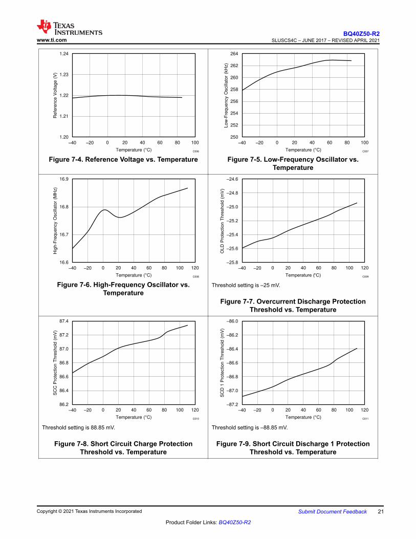
Threshold setting is –25 mV.
Figure 7-7. Overcurrent Discharge ProtectionThreshold vs. Temperature
86.2
86.4
86.6
86.8
87.0
87.2
87.4
±40 ±20 0 20 40 60 80 100 120
SC
C P
rote
ction T
hre
shold
(m
V)
Temperature (C) C010
Threshold setting is 88.85 mV.
Figure 7-8. Short Circuit Charge ProtectionThreshold vs. Temperature
±87.2
±87.0
±86.8
±86.6
±86.4
±86.2
±86.0
±40 ±20 0 20 40 60 80 100 120
SC
D 1
Pro
tection T
hre
shold
(m
V)
Temperature (C) C011
Threshold setting is –88.85 mV.
Figure 7-9. Short Circuit Discharge 1 ProtectionThreshold vs. Temperature
www.ti.comBQ40Z50-R2
SLUSCS4C – JUNE 2017 – REVISED APRIL 2021
Copyright © 2021 Texas Instruments Incorporated Submit Document Feedback 21
Product Folder Links: BQ40Z50-R2

±173.6
±173.5
±173.4
±173.3
±173.2
±173.1
±173.0
±172.9
±40 ±20 0 20 40 60 80 100 120
SC
D 2
Pro
tection T
hre
shold
(m
V)
Temperature (C) C012
Threshold setting is –177.7 mV.
Figure 7-10. Short Circuit Discharge 2 ProtectionThreshold vs. Temperature
10.70
10.75
10.80
10.85
10.90
10.95
11.00
±40 ±20 0 20 40 60 80 100 120
Over-
Cu
rrent
De
lay
Tim
e (
mS
)
Temperature (C) C013
Threshold setting is 11 ms.
Figure 7-11. Overcurrent Delay Time vs.Temperature
432
434
436
438
440
442
444
446
448
450
452
±40 ±20 0 20 40 60 80 100 120
SC
Ch
arg
e C
urr
ent
De
lay
Tim
e (
S)
Temperature (C) C014
Threshold setting is 465 µs.
Figure 7-12. Short Circuit Charge Current DelayTime vs. Temperature
400
420
440
460
480
±40 ±20 0 20 40 60 80 100 120
SC
Dis
charg
e 1
De
lay
Tim
e (
S)
Temperature (C) C015
Threshold setting is 465 µs (including internal delay).
Figure 7-13. Short Circuit Discharge 1 Delay Timevs. Temperature
2.498
2.49805
2.4981
2.49815
2.4982
2.49825
2.4983
2.49835
2.4984
±40 ±20 0 20 40 60 80 100 120
Cell
Voltage (
V)
Temperature (C) C016
Figure 7-14. VCELL Measurement at 2.5-V vs.Temperature
3.498
3.49805
3.4981
3.49815
3.4982
3.49825
±40 ±20 0 20 40 60 80 100 120
Ce
ll V
oltage (
V)
Temperature (C) C017
This is the VCELL average for single cell.
Figure 7-15. VCELL Measurement at 3.5-V vs.Temperature
BQ40Z50-R2SLUSCS4C – JUNE 2017 – REVISED APRIL 2021 www.ti.com
22 Submit Document Feedback Copyright © 2021 Texas Instruments Incorporated
Product Folder Links: BQ40Z50-R2

4.2478
4.24785
4.2479
4.24795
4.248
4.24805
±40 ±20 0 20 40 60 80 100 120
Ce
ll V
oltage (
V)
Temperature (C) C018
This is the VCELL average for single cell.
Figure 7-16. VCELL Measurement at 4.25-V vs.Temperature
99.00
99.05
99.10
99.15
99.20
99.25
±40 ±20 0 20 40 60 80 100 120
Measure
ment
Curr
ent
(mA
)
Temperature (C) C019
ISET = 100 mA
Figure 7-17. I measured vs. Temperature
www.ti.comBQ40Z50-R2
SLUSCS4C – JUNE 2017 – REVISED APRIL 2021
Copyright © 2021 Texas Instruments Incorporated Submit Document Feedback 23
Product Folder Links: BQ40Z50-R2

8 Detailed Description8.1 OverviewThe BQ40Z50-R2 device, incorporating patented Impedance Track™ technology, provides cell balancing whilecharging or at rest. This fully integrated, single-chip, pack-based solution, including a diagnostic lifetime datamonitor and black box recorder, provides a rich array of features for gas gauging, protection, and authenticationfor 1-series, 2-series, 3-series, and 4-series cell Li-ion and Li-polymer battery packs.
8.2 Functional Block Diagram
DMAddr (16bit)
Cell
Balancing
Over
Current
Comparator
Short Circuit
Comparator
Power On
Reset
VoltageReference2
Watchdog
Timer
Zero Volt
ChargeControl
Wake
Comparator
InternalTemp
Sensor
Random
NumberGenerator
AFE ControlADC MUX
Cell Detach
Detection
High
Frequency
Oscillator
SBS COM
Engine
AFE COM
Engine
I/O &
Interrupt
Controller
Data Flash
EEPROM
ADC/CC
Digital Filter
Program
FlashEEPROM
bqBMP
CPU
Timers&
PWM
PMAddr(16bit)
PMInstr(8bit)
Cell, Stack,
Pack
Voltage
VoltageReference1
SMBC
SMBD
LEDCNTLA
LEDCNTLB
LEDCNTLC
PRES or SHUTDN
BTP_INT
FUSE
PTCEN
SRP
PC
HG
DS
G
CH
G
VS
S
PA
CK
BA
T
VC
C
VC
4
VC
3
VC
2
VC
1High Side
N-CH FET
Drive
P-CH
FET Drive
FUSE
Control
High
Voltage
I/O
LED Display
Drive I/O
PB
I
Power Mode
Control
SBS High
Voltage
Translation
Low
Frequency
Oscillator
ADC/CC
FRONTEND
1.8V LDO
Regulator
TS1
TS2
TS3
TS4
Low Voltage
I/O
PTC
Overtemp PTC
SRN
AFE COM
Engine
Data
SRAM
Data (8bit)
I /O
NTC Bias
Copyright © 2017, Texas Instruments Incorporated
DISP
BQ40Z50-R2SLUSCS4C – JUNE 2017 – REVISED APRIL 2021 www.ti.com
24 Submit Document Feedback Copyright © 2021 Texas Instruments Incorporated
Product Folder Links: BQ40Z50-R2
8.3 Feature Description8.3.1 Primary (1st Level) Safety Features
The BQ40Z50-R2 supports a wide range of battery and system protection features that can easily be configured.See the BQ40Z50-R2 Technical Reference Manual (SLUUBK0) for detailed descriptions of each protectionfunction.
The primary safety features include:
• Cell Overvoltage Protection• Cell Undervoltage Protection• Cell Undervoltage Protection Compensated• Overcurrent in Charge Protection• Overcurrent in Discharge Protection• Overload in Discharge Protection• Short Circuit in Charge Protection• Short Circuit in Discharge Protection• Overtemperature in Charge Protection• Overtemperature in Discharge Protection• Undertemperature in Charge Protection• Undertemperature in Discharge Protection• Overtemperature FET protection• Precharge Timeout Protection• Host Watchdog Timeout Protection• Fast Charge Timeout Protection• Overcharge Protection• Overcharging Voltage Protection• Overcharging Current Protection• Over Precharge Current Protection
8.3.2 Secondary (2nd Level) Safety Features
The secondary safety features of the BQ40Z50-R2 can be used to indicate more serious faults via the FUSEpin. This pin can be used to blow an in-line fuse to permanently disable the battery pack from charging ordischarging. See the BQ40Z50-R2 Technical Reference Manual (SLUUBK0) for detailed descriptions of eachprotection function.
The secondary safety features provide protection against:• Safety Overvoltage Permanent Failure• Safety Undervoltage Permanent Failure• Safety Overtemperature Permanent Failure• Safety FET Overtemperature Permanent Failure• Qmax Imbalance Permanent Failure• Impedance Imbalance Permanent Failure• Capacity Degradation Permanent Failure• Cell Balancing Permanent Failure• Fuse Failure Permanent Failure• PTC Permanent Failure• Voltage Imbalance At Rest Permanent Failure• Voltage Imbalance Active Permanent Failure• Charge FET Permanent Failure• Discharge FET Permanent Failure• AFE Register Permanent Failure• AFE Communication Permanent Failure• Second Level Protector Permanent Failure• Instruction Flash Checksum Permanent Failure• Open Cell Connection Permanent Failure
www.ti.comBQ40Z50-R2
SLUSCS4C – JUNE 2017 – REVISED APRIL 2021
Copyright © 2021 Texas Instruments Incorporated Submit Document Feedback 25
Product Folder Links: BQ40Z50-R2

• Data Flash Permanent Failure• Open Thermistor Permanent Failure
8.3.3 Charge Control Features
The BQ40Z50-R2 charge control features include:
• Supports JEITA temperature ranges. Reports charging voltage and charging current according to the activetemperature range
• Handles more complex charging profiles. Allows for splitting the standard temperature range into two sub-ranges and allows for varying the charging current according to the cell voltage
• Reports the appropriate charging current needed for constant current charging and the appropriate chargingvoltage needed for constant voltage charging to a smart charger using SMBus broadcasts
• Reduces the charge difference of the battery cells in a fully charged state of the battery pack gradually usinga voltage-based cell balancing algorithm during charging. A voltage threshold can be set up for cell balancingto be active. This prevents fully charged cells from overcharging and causing excessive degradation and alsoincreases the usable pack energy by preventing premature charge termination.
• Supports precharging/0-volt charging• Supports charge inhibit and charge suspend if battery pack temperature is out of temperature range• Reports charging fault and also indicates charge status via charge and discharge alarms
8.3.4 Gas Gauging
The BQ40Z50-R2 uses the Impedance Track algorithm to measure and calculate the available capacity inbattery cells. The BQ40Z50-R2 accumulates a measure of charge and discharge currents and compensates thecharge current measurement for the temperature and state-of-charge of the battery. The BQ40Z50-R2 estimatesself-discharge of the battery and also adjusts the self-discharge estimation based on temperature. The devicealso has TURBO Mode 2.0 support, which enables the BQ40Z50-R2 to provide the necessary data for theMCU to determine what level of peak power consumption can be applied without causing a system reset ortransient battery voltage level spike to trigger termination flags. See the BQ40Z50-R2 Technical ReferenceManual (SLUUBK0) for further details.
8.3.5 Configuration8.3.5.1 Oscillator Function
The BQ40Z50-R2 fully integrates the system oscillators and does not require any external components tosupport this feature.
8.3.5.2 System Present Operation
The BQ40Z50-R2 checks the PRES pin periodically (1 s). If PRES input is pulled to ground by the externalsystem, the BQ40Z50-R2 detects this as system present.
8.3.5.3 Emergency Shutdown
For battery maintenance, the emergency shutdown feature enables a push button action connecting theSHUTDN pin to shut down an embedded battery pack system before removing the battery. A high-to-lowtransition of the SHUTDN pin signals the BQ40Z50-R2 to turn off the CHG and DSG FETs, disconnecting thepower from the system to safely remove the battery pack. The CHG and DSG FETs can be turned on again byanother high-to-low transition detected by the SHUTDN pin or when a data flash configurable timeout is reached.
8.3.5.4 1-Series, 2-Series, 3-Series, or 4-Series Cell Configuration
In a 1-series cell configuration, VC4 is shorted to VC, VC2, and VC1. In a 2-series cell configuration, VC4 isshorted to VC3 and VC2. In a 3-series cell configuration, VC4 is shorted to VC3.
8.3.5.5 Cell Balancing
The device supports cell balancing by bypassing the current of each cell during charging or at rest. If thedevice's internal bypass is used, up to 10 mA can be bypassed and multiple cells can be bypassed at the sametime. Higher cell balance current can be achieved by using an external cell balancing circuit. In external cellbalancing mode, only one cell at a time can be balanced.
BQ40Z50-R2SLUSCS4C – JUNE 2017 – REVISED APRIL 2021 www.ti.com
26 Submit Document Feedback Copyright © 2021 Texas Instruments Incorporated
Product Folder Links: BQ40Z50-R2

The cell balancing algorithm determines the amount of charge needed to be bypassed to balance the capacity ofall cells.
8.3.6 Battery Parameter Measurements8.3.6.1 Charge and Discharge Counting
The BQ40Z50-R2 uses an integrating delta-sigma analog-to-digital converter (ADC) for current measurement,and a second delta-sigma ADC for individual cell and battery voltage and temperature measurement.
The integrating delta-sigma ADC measures the charge/discharge flow of the battery by measuring the voltagedrop across a small-value sense resistor between the SRP and SRN terminals. The integrating ADC measuresbipolar signals from –0.1 V to 0.1 V. The BQ40Z50-R2 detects charge activity when VSR = V(SRP) – V(SRN)is positive, and discharge activity when VSR = V(SRP) – V(SRN) is negative. The BQ40Z50-R2 continuouslyintegrates the signal over time, using an internal counter. The fundamental rate of the counter is 0.26 nVh.
8.3.7 Battery Trip Point (BTP)
Required for WIN8 OS, the battery trip point (BTP) feature indicates when the RSOC of a battery pack hasdepleted to a certain value set in a DF register. This feature enables a host to program two capacity-basedthresholds that govern the triggering of a BTP interrupt on the BTP_INT pin, and the setting or clearing of theOperationStatus[BTP_INT] on the basis of RemainingCapacity().
An internal weak pullup is applied when the BTP feature is active. Depending on the system design, an externalpullup may be required to put on the BTP_INT pin. See Section 7.12 for details.
8.3.8 Lifetime Data Logging Features
The BQ40Z50-R2 offers lifetime data logging for several critical battery parameters. The following parametersare updated every 10 hours if a difference is detected between values in RAM and data flash:• Maximum and Minimum Cell Voltages• Maximum Delta Cell Voltage• Maximum Charge Current• Maximum Discharge Current• Maximum Average Discharge Current• Maximum Average Discharge Power• Maximum and Minimum Cell Temperature• Maximum Delta Cell Temperature• Maximum and Minimum Internal Sensor Temperature• Maximum FET Temperature• Number of Safety Events Occurrences and the Last Cycle of the Occurrence• Number of Valid Charge Termination and the Last Cycle of the Valid Charge Termination• Number of Qmax and Ra Updates and the Last Cycle of the Qmax and Ra Updates• Number of Shutdown Events• Cell Balancing Time for Each Cell
(This data is updated every 2 hours if a difference is detected.)• Total FW Runtime and Time Spent in Each Temperature Range
(This data is updated every 2 hours if a difference is detected.)
8.3.9 Authentication
The BQ40Z50-R2 supports authentication by the host using SHA-1.
8.3.10 LED Display
The BQ40Z50-R2 can drive a 3-, 4-, or 5- segment LED display for remaining capacity indication and/or apermanent fail (PF) error code indication.
8.3.11 IATA Support
The BQ40Z50-R2 supports IATA with several new commands and procedures. See the BQ40Z50-R2 TechnicalReference Manual (SLUUBK0) for further details.
www.ti.comBQ40Z50-R2
SLUSCS4C – JUNE 2017 – REVISED APRIL 2021
Copyright © 2021 Texas Instruments Incorporated Submit Document Feedback 27
Product Folder Links: BQ40Z50-R2

8.3.12 Voltage
The BQ40Z50-R2 updates the individual series cell voltages at 0.25-s intervals. The internal ADC of theBQ40Z50-R2 measures the voltage, and scales and calibrates it appropriately. This data is also used tocalculate the impedance of the cell for the Impedance Track gas gauging.
8.3.13 Current
The BQ40Z50-R2 uses the SRP and SRN inputs to measure and calculate the battery charge and dischargecurrent using a 1-mΩ to 3-mΩ typ. sense resistor.
8.3.14 Temperature
The BQ40Z50-R2 has an internal temperature sensor and inputs for four external temperature sensors. Allfive temperature sensor options can be individually enabled and configured for cell or FET temperature usage.Two configurable thermistor models are provided to allow the monitoring of cell temperature in addition to FETtemperature, which use a different thermistor profile.
8.3.15 Communications
The BQ40Z50-R2 uses SMBus v1.1 with MASTER mode and packet error checking (PEC) options per the SBSspecification.
8.3.15.1 SMBus On and Off State
The BQ40Z50-R2 detects an SMBus off state when SMBC and SMBD are low for two or more seconds. Clearingthis state requires that either SMBC or SMBD transition high. The communication bus will resume activity within1 ms.
8.3.15.2 SBS Commands
See the BQ40Z50-R2 Technical Reference Manual (SLUUBK0) for further details.
8.4 Device Functional ModesThe BQ40Z50-R2 supports three power modes to reduce power consumption:• In NORMAL mode, the BQ40Z50-R2 performs measurements, calculations, protection decisions, and data
updates in 250-ms intervals. Between these intervals, the BQ40Z50-R2 is in a reduced power stage.• In SLEEP mode, the BQ40Z50-R2 performs measurements, calculations, protection decisions, and data
updates in adjustable time intervals. Between these intervals, the BQ40Z50-R2 is in a reduced power stage.The BQ40Z50-R2 has a wake function that enables exit from SLEEP mode when current flow or failure isdetected.
• In SHUTDOWN mode, the BQ40Z50-R2 is completely disabled.
See the BQ40Z50-R2 Technical Reference Manual (SLUUBK0) for further details.
BQ40Z50-R2SLUSCS4C – JUNE 2017 – REVISED APRIL 2021 www.ti.com
28 Submit Document Feedback Copyright © 2021 Texas Instruments Incorporated
Product Folder Links: BQ40Z50-R2

9 Application and ImplementationNote
Information in the following applications sections is not part of the TI component specification,and TI does not warrant its accuracy or completeness. TI’s customers are responsible fordetermining suitability of components for their purposes, as well as validating and testing their designimplementation to confirm system functionality.
9.1 Application InformationThe BQ40Z50-R2 is a gas gauge with primary protection support, and can be used with 1-series to 4-seriesLi-ion/Li-polymer battery packs. To implement and design a comprehensive set of parameters for a specificbattery pack, users need the Battery Management Studio (BQSTUDIO) graphical user-interface tool installed ona PC during development. The firmware installed on the BQSTUDIO tool has default values for this product,which are summarized in the BQ40Z50-R2 Technical Reference Manual (SLUUBK0). Using the BQSTUDIO tool,these default values can be changed to cater to specific application requirements during development oncethe system parameters, such as fault trigger thresholds for protection, enable/disable of certain features foroperation, configuration of cells, chemistry that best matches the cell used, and more are known. This data isreferred to as the "golden image."
www.ti.comBQ40Z50-R2
SLUSCS4C – JUNE 2017 – REVISED APRIL 2021
Copyright © 2021 Texas Instruments Incorporated Submit Document Feedback 29
Product Folder Links: BQ40Z50-R2

9.2 Typical Applications
2P
1P
1N
4P
3P
Sys
Pre
sP
AC
K-
PA
CK
+
1
1
IC g
round s
hould
be c
onnecte
d to
the 1
N c
ell ta
b.
Pla
ce R
T1 c
lose to
Q2 a
nd Q
3.
2
LE
D3
LE
D5
LE
D2
LE
D4
LE
D1
GN
D
GN
D
CH
GN
D
CH
GN
D
GN
DG
ND
GN
D
GN
D
CH
GN
D
GN
D
AG
ND
GN
D
NT
1
PA
CK
-
P
AC
K+
L
ED
DIS
PLA
Y
11
PA
CK
-
SM
BD
SM
BC
3R
epla
ce D
1 a
nd R
13 w
ith a
10 o
hm
resisto
r for s
ingle
cell a
pplic
atio
ns
3
3
PR
ES
/ SH
UT
DO
WN
BT
P_IN
T
GN
D
SH
UT
DO
WN
PR
ES
/ SH
UT
DO
WN
100
R2
1.0
kR
7
1.0
kR
9
1.0
kR
16
1.0
kR
17
0.1
uF
C5
0.1
uF
C6
0.1
uF
C10
0.1
uF
C11
0.1
uF
C9
30V
D1
2.2
uF
C13
5.1
k
R18
5.1
k
R19
51k
R10
0.1
uF
C7
5.1
kR
11
5.1
kR
12
100
R13
10
Me
g
R6
5.1
kR
14
10M
eg
R3
300
R1
3
1
2
-30V
Q1
0.1
uF
C1
0.1
uF
C2
10M
eg
R4
3
1
2
Q4
10k
R5
10k
R15
1
4
3
2
F1
0.1
uF
C3
0.1
uF
C4
200
R8
41
32
0.1
uF
C12
D4
D3
D2
D5
D6
41
32
100
R26
100
R27
0.1
uF
C18
0.0
01
R28
100
R20
100
R21
100
R22
100
R23
VD
D1
V4
2
V3
3
V2
4V
15
VS
S6
CD
7
OU
T8
PAD9
U1
10.0k ohm
t°
RT
2
10.0k ohm
t°
RT
310.0k ohm
t°
RT
4
10.0k ohm
t°
RT
5
5 4 123
J2
0.1
uF
C8
100
R24
100
R25
12
U4
12
U5
41 2 3
J3
12
U2
541 2 3
J1
4
7,8
1,2
,3
5,6
,
Q3
4
7,8
1,2
,3
5,6
,
Q2
t°
RT
1
PB
I1
VC
42
VC
33
VC
24
VC
15
SR
N6
NC
7
SR
P8
VS
S9
TS
11
0
TS
211
TS
31
2
TS
41
3
NC
14
BT
P_
INT
15
PR
ES
/SH
UT
DN
16
DIS
P1
7
SM
BD
18
SM
BC
19
LE
DC
NT
LA
20
LE
DC
NT
LB
21
LE
DC
NT
LC
22
PT
C2
3
PT
CE
N2
4
FU
SE
25
VC
C2
6
PA
CK
27
DS
G2
8
NC
29
PC
HG
30
CH
G3
1
BA
T3
2
PA
D3
3
U3
3
5,6,84,71,2, Q
5
GN
DG
ND
GN
D
0.1
uF
C14
0.1
uF
C15
0.1
uF
C16
0.1
uF
C17
2
Co
pyrig
ht ©
20
17
,Te
xa
s In
stru
me
nts
Inco
rpo
rate
d
Figure 9-1. Application Schematic
BQ40Z50-R2SLUSCS4C – JUNE 2017 – REVISED APRIL 2021 www.ti.com
30 Submit Document Feedback Copyright © 2021 Texas Instruments Incorporated
Product Folder Links: BQ40Z50-R2

9.2.1 Design Requirements
Table 9-1 shows the default settings for the main parameters. Use the BQSTUDIO tool to update the settings tomeet the specific application or battery pack configuration requirements.
The device should be calibrated before any gauging test. Follow the procedures on the BQSTUDIO Calibrationpage to calibrate the device, and use the information on the BQSTUDIO Chemistry page to update the matchchemistry profile to the device.
Table 9-1. Design ParametersDESIGN PARAMETER EXAMPLE
Cell Configuration 3s1p (3-series with 1 parallel)(1)
Design Capacity 4400 mAh
Device Chemistry 1210 (LiCoO2/graphitized carbon)
Cell Overvoltage at Standard Temperature 4300 mV
Cell Undervoltage 2500 mV
Shutdown Voltage 2300 mV
Overcurrent in CHARGE Mode 6000 mA
Overcurrent in DISCHARGE Mode –6000 mA
Short Circuit in CHARGE Mode 0.1 V/Rsense across SRP, SRN
Short Circuit in DISCHARGE Mode 0.1 V/Rsense across SRP, SRN
Safety Overvoltage 4500 mV
Cell Balancing Disabled
Internal and External Temperature Sensor External temperature sensor is used.
Undertemperature Charging 0°C
Undertemperature Discharging 0°C
BROADCAST Mode Disabled
Battery Trip Point (BTP) with active high interrupt Disabled
(1) When using the device the first time and if a 1-s or 2-s battery pack is used, then a charger or power supply should be connectedto the PACK+ terminal to prevent device shutdown. Then update the cell configuration (see the BQ40Z50-R2 Technical ReferenceManual [SLUUBK0] for details) before removing the charger connection.
9.2.2 Detailed Design Procedure9.2.2.1 High-Current Path
The high-current path begins at the PACK+ terminal of the battery pack. As charge current travels through thepack, it finds its way through protection FETs, a chemical fuse, the Li-ion cells and cell connections, and thesense resistor, and then returns to the PACK– terminal (see Figure 9-2). In addition, some components areplaced across the PACK+ and PACK– terminals to reduce effects from electrostatic discharge.
9.2.2.1.1 Protection FETs
Select the N-channel charge and discharge FETs for a given application. Most portable battery applications are agood match for the CSD17308Q3. The TI CSD17308Q3 is a 47A, 30-V device with Rds(on) of 8.2 mΩ when thegate drive voltage is 8 V.
If a precharge FET is used, R1 is calculated to limit the precharge current to the desired rate. Be sure to accountfor the power dissipation of the series resistor. The precharge current is limited to (VCHARGER – VBAT)/R1 andmaximum power dissipation is (Vcharger – Vbat)2/R1.
The gates of all protection FETs are pulled to the source with a high-value resistor between the gate and sourceto ensure they are turned off if the gate drive is open.
Capacitors C1 and C2 help protect the FETs during an ESD event. Using two devices ensures normal operationif one becomes shorted. To have good ESD protection, the copper trace inductance of the capacitor leads
www.ti.comBQ40Z50-R2
SLUSCS4C – JUNE 2017 – REVISED APRIL 2021
Copyright © 2021 Texas Instruments Incorporated Submit Document Feedback 31
Product Folder Links: BQ40Z50-R2
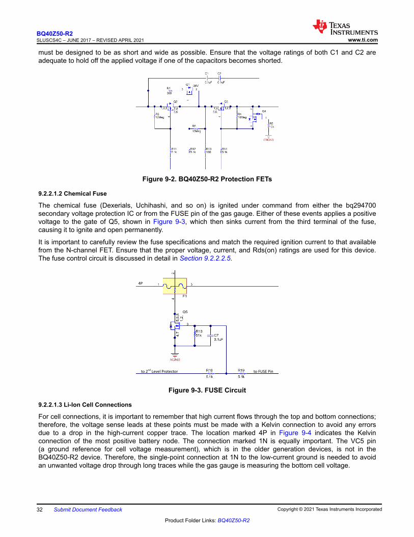
must be designed to be as short and wide as possible. Ensure that the voltage ratings of both C1 and C2 areadequate to hold off the applied voltage if one of the capacitors becomes shorted.
Figure 9-2. BQ40Z50-R2 Protection FETs
9.2.2.1.2 Chemical Fuse
The chemical fuse (Dexerials, Uchihashi, and so on) is ignited under command from either the bq294700secondary voltage protection IC or from the FUSE pin of the gas gauge. Either of these events applies a positivevoltage to the gate of Q5, shown in Figure 9-3, which then sinks current from the third terminal of the fuse,causing it to ignite and open permanently.
It is important to carefully review the fuse specifications and match the required ignition current to that availablefrom the N-channel FET. Ensure that the proper voltage, current, and Rds(on) ratings are used for this device.The fuse control circuit is discussed in detail in Section 9.2.2.2.5.
4P
to 2nd
Level Protector to FUSE Pin
Figure 9-3. FUSE Circuit
9.2.2.1.3 Li-Ion Cell Connections
For cell connections, it is important to remember that high current flows through the top and bottom connections;therefore, the voltage sense leads at these points must be made with a Kelvin connection to avoid any errorsdue to a drop in the high-current copper trace. The location marked 4P in Figure 9-4 indicates the Kelvinconnection of the most positive battery node. The connection marked 1N is equally important. The VC5 pin(a ground reference for cell voltage measurement), which is in the older generation devices, is not in theBQ40Z50-R2 device. Therefore, the single-point connection at 1N to the low-current ground is needed to avoidan unwanted voltage drop through long traces while the gas gauge is measuring the bottom cell voltage.
BQ40Z50-R2SLUSCS4C – JUNE 2017 – REVISED APRIL 2021 www.ti.com
32 Submit Document Feedback Copyright © 2021 Texas Instruments Incorporated
Product Folder Links: BQ40Z50-R2

Figure 9-4. Li-Ion Cell Connections
9.2.2.1.4 Sense Resistor
As with the cell connections, the quality of the Kelvin connections at the sense resistor is critical. The senseresistor must have a temperature coefficient no greater than 50 ppm in order to minimize current measurementdrift with temperature. Choose the value of the sense resistor to correspond to the available overcurrent andshort-circuit ranges of the BQ40Z50-R2 device. Select the smallest value possible to minimize the negativevoltage generated on the BQ40Z50-R2 VSS node(s) during a short circuit. This pin has an absolute minimumof –0.3 V. Parallel resistors can be used as long as good Kelvin sensing is ensured. The device is designed tosupport a 1-mΩ to 3-mΩ sense resistor.
The BQ40Z50-R2 ground scheme is different from that of the older generation devices. In previous devices,the device ground (or low current ground) is connected to the SRN side of the RSENSE resistor pad. In theBQ40Z50-R2 device, however, it connects the low-current ground on the SRP side of the RSENSE resistor padclose to the battery 1N terminal (see Section 9.2.2.1.3). This is because the BQ40Z50-R2 device has one lessVC pin (a ground reference pin VC5) compared to the previous devices. The pin was removed and was internallycombined to SRP.
Figure 9-5. Sense Resistor
9.2.2.1.5 ESD Mitigation
A pair of series 0.1-μF ceramic capacitors is placed across the PACK+ and PACK– terminals to help in themitigation of external electrostatic discharges. The two devices in series ensure continued operation of the packif one of the capacitors becomes shorted.
Optionally, a tranzorb such as the SMBJ2A can be placed across the terminals to further improve ESD immunity.
9.2.2.2 Gas Gauge Circuit
The gas gauge circuit includes the BQ40Z50-R2 and its peripheral components. These components are dividedinto the following groups: differential low-pass filter, PBI, system present, SMBus communication, fuse circuit,and LED.
9.2.2.2.1 Coulomb-Counting Interface
The BQ40Z50-R2 uses an integrating delta-sigma ADC for current measurements. Add a 100-Ω resistor fromthe sense resistor to the SRP and SRN inputs of the device. Place a 0.1-µF (C18) filter capacitor across the SRPand SRN inputs.
www.ti.comBQ40Z50-R2
SLUSCS4C – JUNE 2017 – REVISED APRIL 2021
Copyright © 2021 Texas Instruments Incorporated Submit Document Feedback 33
Product Folder Links: BQ40Z50-R2
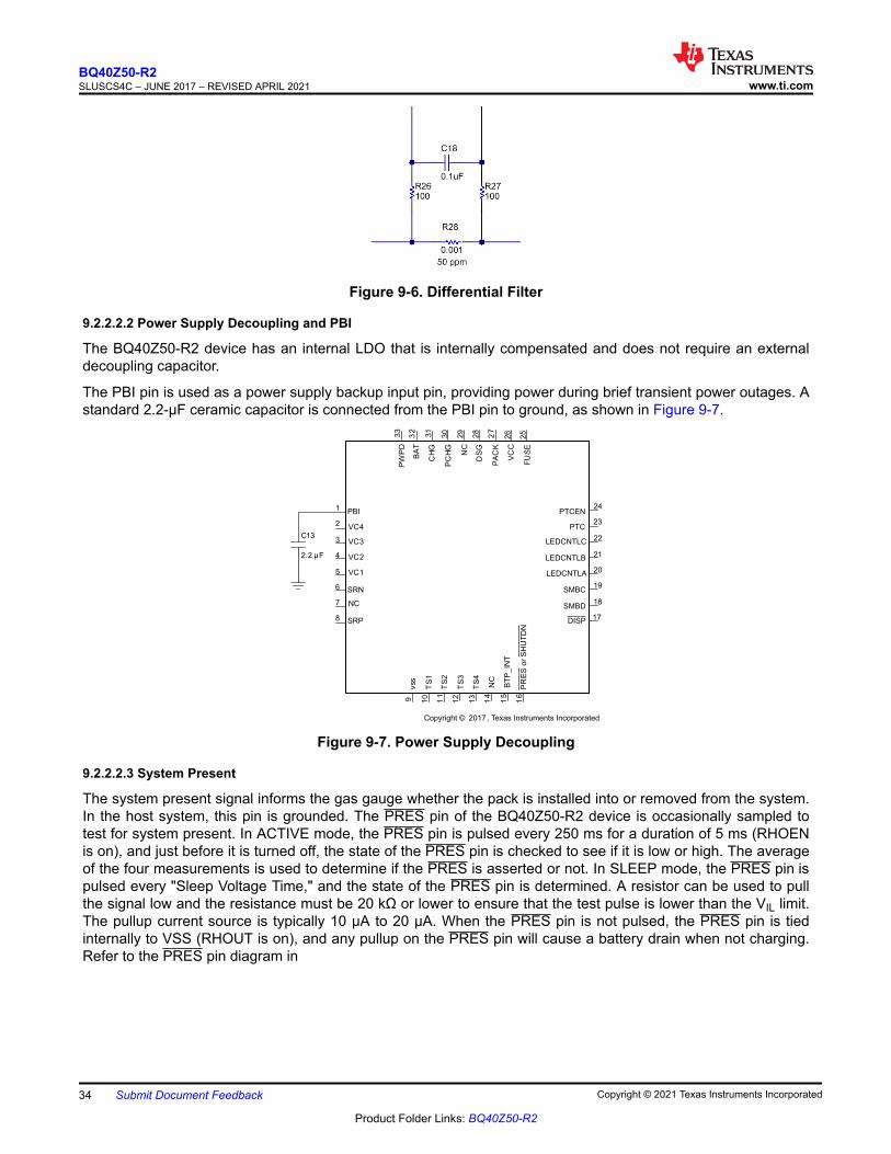
Figure 9-6. Differential Filter
9.2.2.2.2 Power Supply Decoupling and PBI
The BQ40Z50-R2 device has an internal LDO that is internally compensated and does not require an externaldecoupling capacitor.
The PBI pin is used as a power supply backup input pin, providing power during brief transient power outages. Astandard 2.2-µF ceramic capacitor is connected from the PBI pin to ground, as shown in Figure 9-7.
Copyright © 2017, Texas Instruments Incorporated
C13
2.2 μF
1
2
3
4
5
6
7
8
vss
TS
1
TS
2
TS
3
TS
4
NC
BT
P_
INT
PR
ES
or
SH
UT
DN
9 10
11
12
13
14
15
16
PBI
VC4
VC3
VC2
VC1
SRN
NC
SRP
PW
PD
BA
T
CH
G
PC
HG
NC
DS
G
PA
CK
VC
C
FU
SE
PTCEN
PTC
LEDCNTLC
LEDCNTLB
LEDCNTLA
SMBC
SMBD
DISP
33
32
31
30
29
28
27
26
25
24
23
22
21
20
19
18
17
Figure 9-7. Power Supply Decoupling
9.2.2.2.3 System Present
The system present signal informs the gas gauge whether the pack is installed into or removed from the system.In the host system, this pin is grounded. The PRES pin of the BQ40Z50-R2 device is occasionally sampled totest for system present. In ACTIVE mode, the PRES pin is pulsed every 250 ms for a duration of 5 ms (RHOENis on), and just before it is turned off, the state of the PRES pin is checked to see if it is low or high. The averageof the four measurements is used to determine if the PRES is asserted or not. In SLEEP mode, the PRES pin ispulsed every "Sleep Voltage Time," and the state of the PRES pin is determined. A resistor can be used to pullthe signal low and the resistance must be 20 kΩ or lower to ensure that the test pulse is lower than the VIL limit.The pullup current source is typically 10 µA to 20 µA. When the PRES pin is not pulsed, the PRES pin is tiedinternally to VSS (RHOUT is on), and any pullup on the PRES pin will cause a battery drain when not charging.Refer to the PRES pin diagram in
BQ40Z50-R2SLUSCS4C – JUNE 2017 – REVISED APRIL 2021 www.ti.com
34 Submit Document Feedback Copyright © 2021 Texas Instruments Incorporated
Product Folder Links: BQ40Z50-R2

<20 K
13
14
15
16
VIL
TS
4
NC
BT
P_IN
T
PR
ES
Figure 9-8. System Present Pull-Down Resistor
Because the System Present signal is part of the pack connector interface to the outside world, it must beprotected from external electrostatic discharge events. The PRES pin has integrated ESD protection to 2 kV.External protection can be added to support higher ESD protection requirements. The TPD1E10B06 single-channel ESD protection diode (U2) can protect the input up to 30 kV, and the R8 reduces the holding current torelease the internal SCR in the event that it triggers.
to Discharge FET
Figure 9-9. System Present ESD and Short Protection
9.2.2.2.4 SMBus Communication
The SMBus clock and data pins have integrated high-voltage ESD protection circuits; however, addingTPD1E10B06 ESD protection diodes (U4 and U5) and series resistors (R24 and R25) provides more robustESD performance.
www.ti.comBQ40Z50-R2
SLUSCS4C – JUNE 2017 – REVISED APRIL 2021
Copyright © 2021 Texas Instruments Incorporated Submit Document Feedback 35
Product Folder Links: BQ40Z50-R2

The SMBus clock and data lines have internal pulldown. When the gas gauge senses that both lines are low(such as during removal of the pack), the device performs auto-offset calibration and then goes into SLEEPmode to conserve power.
Figure 9-10. ESD Protection for SMBus Communication
9.2.2.2.5 FUSE Circuitry
The FUSE pin of the BQ40Z50-R2 device is designed to ignite the chemical fuse if one of the various safetycriteria is violated. The FUSE pin also monitors the state of the secondary-voltage protection IC. Q5 ignites thechemical fuse when its gate is high. The 7-V output of the bq294700 is divided by R18 and R19, which providesadequate gate drive for Q5 while guarding against excessive back current into the bq294700 if the FUSE signalis high.
Using C7 is generally a good practice, especially for RFI immunity. C7 may be removed, if desired, because thechemical fuse is a comparatively slow device and is not affected by any sub-microsecond glitches that comefrom the FUSE output during the cell connection process.
If the AFEFUSE output is not used, it should be connected to VSS.
4P
to 2nd
Level Protector to FUSE Pin
Figure 9-11. FUSE Circuit
When the BQ40Z50-R2 device is commanded to ignite the chemical fuse, the FUSE pin activates to give atypical 8-V output. The new design makes it possible to use a higher Vgs FET for Q5. This improves therobustness of the system, as well as widens the choices for Q5.
9.2.2.3 Secondary-Current Protection
The BQ40Z50-R2 device provides secondary overcurrent and short-circuit protection, cell balancing, cell voltagemultiplexing, and voltage translation. The following section examines cell and battery inputs, pack and FETcontrol, temperature output, and cell balancing.
BQ40Z50-R2SLUSCS4C – JUNE 2017 – REVISED APRIL 2021 www.ti.com
36 Submit Document Feedback Copyright © 2021 Texas Instruments Incorporated
Product Folder Links: BQ40Z50-R2

9.2.2.3.1 Cell and Battery Inputs
Each cell input is conditioned with a simple RC filter, which provides ESD protection during cell connect and actsto filter unwanted voltage transients. The resistor value allows some trade-off for cell balancing versus safetyprotection.
The integrated cell balancing FETs enable the AFE to bypass cell current around a given cell or numerous cells,effectively balancing the entire battery stack. External series resistors placed between the cell connections andthe VCx I/O pins set the balancing current magnitude. The internal FETs provide a 200-Ω resistance (2 V < VDS< 4 V). Series input resistors between 100 Ω and 300 Ω are recommended for effective cell balancing.
The BAT input uses a diode (D1) to isolate and decouple it from the cells in the event of a transient dip in voltagecaused by a short-circuit event.
Also, as described in Section 9.2.2.1, the top and bottom nodes of the cells must be sensed at the batteryconnections with a Kelvin connection to prevent voltage sensing errors caused by a drop in the high-current PCBcopper.
Figure 9-12. Cell and BAT Inputs
9.2.2.3.2 External Cell Balancing
Internal cell balancing can only support up to 10 mA. External cell balancing is provided as another option forfaster cell balancing. For details, refer to the application note, Fast Cell Balancing Using External MOSFET(SLUA420).
9.2.2.3.3 PACK and FET Control
The PACK and VCC inputs provide power to the BQ40Z50-R2 device from the charger. The PACK input alsoprovides a method to measure and detect the presence of a charger. The PACK input uses a 10-kΩ resistor;whereas, the VCC input uses an internal diode to guard against input transients and prevent a misoperation ofthe gate driver during short-circuit events.
www.ti.comBQ40Z50-R2
SLUSCS4C – JUNE 2017 – REVISED APRIL 2021
Copyright © 2021 Texas Instruments Incorporated Submit Document Feedback 37
Product Folder Links: BQ40Z50-R2

Figure 9-13. BQ40Z50-R2 PACK and FET Control
The N-channel charge and discharge FETs are controlled with 5.1-kΩ series gate resistors, which provide aswitching time constant of a few microseconds. The 10-MΩ resistors ensure that the FETs are off in the eventof an open connection to the FET drivers. Q4 is provided to protect the discharge FET (Q3) in the event of areverse-connected charger. Without Q4, Q3 can be driven into its linear region and suffer severe damage if thePACK+ input becomes slightly negative.
Q4 turns on in that case to protect Q3 by shorting its gate to source. To use the simple ground gate circuit, theFET must have a low gate turn-on threshold. If it is desired to use a more standard device, such as the 2N7002as the reference schematic, the gate should be biased up to 3.3 V with a high-value resistor. The BQ40Z50-R2device has the capability to provide a current-limited charging path typically used for low battery voltage orlow temperature charging. The BQ40Z50-R2 device uses an external P-channel, precharge FET controlled byPCHG.
9.2.2.3.4 Temperature Output
For the BQ40Z50-R2 device, TS1, TS2, TS3, and TS4 provide thermistor drive-under program control. Eachpin can be enabled with an integrated 18-kΩ (typical) linearization pullup resistor to support the use of a 10-kΩat 25°C (103) NTC external thermistor, such as a Mitsubishi BN35-3H103. The reference design includes four10-kΩ thermistors: RT2, RT3, RT4, and RT5. The BQ40Z50-R2 device supports up to four external thermistors.Connect unused thermistor pins to VSS.
BQ40Z50-R2SLUSCS4C – JUNE 2017 – REVISED APRIL 2021 www.ti.com
38 Submit Document Feedback Copyright © 2021 Texas Instruments Incorporated
Product Folder Links: BQ40Z50-R2

Figure 9-14. Thermistor Drive
9.2.2.3.5 LEDs
Three LED control outputs provide constant current sinks for the driving external LEDs. These outputs areconfigured to provide voltage and control for up to five LEDs. No external bias voltage is required. UnusedLEDCNTL pins can remain open or they can be connected to VSS. The DISP pin should be connected to VSS ifthe LED feature is not used.
Figure 9-15. LEDs
9.2.2.3.6 Safety PTC Thermistor
The BQ40Z50-R2 device provides support for a safety PTC thermistor. The PTC thermistor is connectedbetween the PTC and BAT pins. It can be placed close to the CHG/DSG FETs to monitor the temperature. ThePTC pin monitors the voltage at the pin and will trip if the thermistor resistance exceeds the defined threshold. APTC fault is one of the permanent failure modes. It can only be cleared by a POR.
To disable, connect PTC and PTCEN to VSS.
Figure 9-16. PTC Thermistor
www.ti.comBQ40Z50-R2
SLUSCS4C – JUNE 2017 – REVISED APRIL 2021
Copyright © 2021 Texas Instruments Incorporated Submit Document Feedback 39
Product Folder Links: BQ40Z50-R2

9.2.3 Application Curves
–25.8
–25.6
–25.4
–25.2
–25.0
–24.8
–24.6
–40 –20 0 20 40 60 80 100 120
OLD
Pro
tection
Thre
shold
(mV
)
Temperature (°C) C009
Threshold setting is –25 mV.
Figure 9-17. Overcurrent Discharge ProtectionThreshold vs. Temperature
86.2
86.4
86.6
86.8
87.0
87.2
87.4
±40 ±20 0 20 40 60 80 100 120
SC
C P
rote
ction T
hre
shold
(m
V)
Temperature (C) C010
Threshold setting is 88.85 mV.
Figure 9-18. Short Circuit Charge ProtectionThreshold vs. Temperature
±87.2
±87.0
±86.8
±86.6
±86.4
±86.2
±86.0
±40 ±20 0 20 40 60 80 100 120
SC
D 1
Pro
tection T
hre
shold
(m
V)
Temperature (C) C011
Threshold setting is –88.85 mV.
Figure 9-19. Short Circuit Discharge 1 ProtectionThreshold vs. Temperature
±173.6
±173.5
±173.4
±173.3
±173.2
±173.1
±173.0
±172.9
±40 ±20 0 20 40 60 80 100 120
SC
D 2
Pro
tection T
hre
shold
(m
V)
Temperature (C) C012
Threshold setting is –177.7 mV.
Figure 9-20. Short Circuit Discharge 2 ProtectionThreshold vs. Temperature
10.70
10.75
10.80
10.85
10.90
10.95
11.00
±40 ±20 0 20 40 60 80 100 120
Over-
Cu
rrent
De
lay
Tim
e (
mS
)
Temperature (C) C013
Threshold setting is 11 ms.
Figure 9-21. Overcurrent Delay Time vs.Temperature
432
434
436
438
440
442
444
446
448
450
452
±40 ±20 0 20 40 60 80 100 120
SC
Ch
arg
e C
urr
ent
De
lay
Tim
e (
S)
Temperature (C) C014
Threshold setting is 465 µs.
Figure 9-22. Short Circuit Charge Current DelayTime vs. Temperature
BQ40Z50-R2SLUSCS4C – JUNE 2017 – REVISED APRIL 2021 www.ti.com
40 Submit Document Feedback Copyright © 2021 Texas Instruments Incorporated
Product Folder Links: BQ40Z50-R2

10 Power Supply RecommendationsThe device manages its supply voltage dynamically according to the operation conditions. Normally, the BATinput is the primary power source to the device. The BAT pin should be connected to the positive termination ofthe battery stack. The input voltage for the BAT pin ranges from 2.2 V to 26 V.
The VCC pin is the secondary power input, which activates when the BAT voltage falls below minimum VCC. Thisenables the device to source power from a charger (if present) connected to the PACK pin. The VCC pin shouldbe connected to the common drain of the CHG and DSG FETs. The charger input should be connected to thePACK pin.
www.ti.comBQ40Z50-R2
SLUSCS4C – JUNE 2017 – REVISED APRIL 2021
Copyright © 2021 Texas Instruments Incorporated Submit Document Feedback 41
Product Folder Links: BQ40Z50-R2

11 Layout11.1 Layout GuidelinesA battery fuel gauge circuit board is a challenging environment due to the fundamental incompatibility of high-current traces and ultra-low current semiconductor devices. The best way to protect against unwanted trace-to-trace coupling is with a component placement, such as that shown in Figure 11-1, where the high-current sectionis on the opposite side of the board from the electronic devices. Clearly, this is not possible in many situationsdue to mechanical constraints. Still, every attempt should be made to route high-current traces away from signaltraces, which enter the BQ40Z50-R2 directly. IC references and registers can be disturbed and in rare casesdamaged due to magnetic and capacitive coupling from the high-current path.
Note
During surge current and ESD events, the high-current traces appear inductive and can coupleunwanted noise into sensitive nodes of the gas gauge electronics, as illustrated in Figure 11-2.
Low Level Circuits
BAT +
PA
CK
+
PA
CK
–BAT –
R1J1
C1
F1
Q2 Q1C3C2
Copyright © 2016, Texas Instruments Incorporated
Figure 11-1. Separating High- and Low-Current Sections Provides an Advantage in Noise Immunity
PACK+
COMM
PACK–
Copyright © 2016, Texas Instruments Incorporated
BMU
Figure 11-2. Avoid Close Spacing Between High-Current and Low-Level Signal Lines
Kelvin voltage sensing is extremely important in order to accurately measure current and top and bottom cellvoltages. Place all filter components as close as possible to the device. Route the traces from the sense resistorin parallel to the filter circuit. Adding a ground plane around the filter network can add additional noise immunity.Figure 11-3 and Figure 11-4 demonstrate correct Kelvin current sensing.
BQ40Z50-R2SLUSCS4C – JUNE 2017 – REVISED APRIL 2021 www.ti.com
42 Submit Document Feedback Copyright © 2021 Texas Instruments Incorporated
Product Folder Links: BQ40Z50-R2

Current Direction
To SRP – SRN pin or HSRP – HSRN pin
RSNS
Current Sensing Direction
Figure 11-3. Sensing Resistor PCB Layout
Sense Resistor Ground Shield
Filter Circuit
Figure 11-4. Sense Resistor, Ground Shield, and Filter Circuit Layout
11.1.1 Protector FET Bypass and Pack Terminal Bypass Capacitors
Use wide copper traces to lower the inductance of the bypass capacitor circuit. Figure 11-5 shows an examplelayout, demonstrating this technique.
Copyright © 2016, Texas Instruments Incorporated
Pack+
C2 C3
F1
Pack±
C1
BAT+
Pa
ck+
Pa
ck±
BAT±
Low Level Circuits
C1
J1 R1
F1
Q2
C2Q1
C3
J1
Figure 11-5. Use Wide Copper Traces to Lower the Inductance of Bypass Capacitors C1, C2, and C3
11.1.2 ESD Spark Gap
Protect SMBus clock, data, and other communication lines from ESD with a spark gap at the connector. Thepattern in Figure 11-6 is recommended, with 0.2-mm spacing between the points.
www.ti.comBQ40Z50-R2
SLUSCS4C – JUNE 2017 – REVISED APRIL 2021
Copyright © 2021 Texas Instruments Incorporated Submit Document Feedback 43
Product Folder Links: BQ40Z50-R2

Figure 11-6. Recommended Spark-Gap Pattern Helps Protect Communication Lines from ESD
11.2 Layout Example
CHARGE
AND
DISCHARGE
PATH
CURRENT
FILTER
SENSE
RESISTOR
2ND
LEVEL
PROTECTOR
LEDS
THERMISTORS
Figure 11-7. Top Layer
Figure 11-8. Internal Layer 1
BQ40Z50-R2SLUSCS4C – JUNE 2017 – REVISED APRIL 2021 www.ti.com
44 Submit Document Feedback Copyright © 2021 Texas Instruments Incorporated
Product Folder Links: BQ40Z50-R2

Figure 11-9. Internal Layer 2
FILTER
COMPONENTS
CHARGE
AND
DISCHARGE
PATH
Figure 11-10. Bottom Layer
www.ti.comBQ40Z50-R2
SLUSCS4C – JUNE 2017 – REVISED APRIL 2021
Copyright © 2021 Texas Instruments Incorporated Submit Document Feedback 45
Product Folder Links: BQ40Z50-R2

12 Device and Documentation Support12.1 Third-Party Products DisclaimerTI'S PUBLICATION OF INFORMATION REGARDING THIRD-PARTY PRODUCTS OR SERVICES DOES NOTCONSTITUTE AN ENDORSEMENT REGARDING THE SUITABILITY OF SUCH PRODUCTS OR SERVICESOR A WARRANTY, REPRESENTATION OR ENDORSEMENT OF SUCH PRODUCTS OR SERVICES, EITHERALONE OR IN COMBINATION WITH ANY TI PRODUCT OR SERVICE.
12.2 Documentation Support12.2.1 Related Documentation
For related documentation, see the following from the BQ40Z50-R2 product page on TI.com:• BQ40Z50-R2 Technical Reference Manual (SLUUBK0)• BQ40Z50EVM Li-Ion Battery Pack Manager Evaluation Module User's Guide (SLUUAV7)
12.2.2 Receiving Notification of Documentation Updates
To receive notification of documentation updates, navigate to the device product folder on ti.com. In the upperright corner, click on Alert me to register and receive a weekly digest of any product information that haschanged. For change details, review the revision history included in any revised document.
12.3 Support ResourcesTI E2E™ support forums are an engineer's go-to source for fast, verified answers and design help — straightfrom the experts. Search existing answers or ask your own question to get the quick design help you need.
Linked content is provided "AS IS" by the respective contributors. They do not constitute TI specifications and donot necessarily reflect TI's views; see TI's Terms of Use.
12.4 TrademarksImpedance Track™ and TI E2E™ are trademarks of Texas Instruments.All trademarks are the property of their respective owners.12.5 Electrostatic Discharge Caution
This integrated circuit can be damaged by ESD. Texas Instruments recommends that all integrated circuits be handledwith appropriate precautions. Failure to observe proper handling and installation procedures can cause damage.ESD damage can range from subtle performance degradation to complete device failure. Precision integrated circuits maybe more susceptible to damage because very small parametric changes could cause the device not to meet its publishedspecifications.
12.6 GlossaryTI Glossary This glossary lists and explains terms, acronyms, and definitions.
13 Mechanical, Packaging, and Orderable InformationThe following pages include mechanical, packaging, and orderable information. This information is the mostcurrent data available for the designated devices. This data is subject to change without notice and revision ofthis document. For browser-based versions of this data sheet, refer to the left-hand navigation.
BQ40Z50-R2SLUSCS4C – JUNE 2017 – REVISED APRIL 2021 www.ti.com
46 Submit Document Feedback Copyright © 2021 Texas Instruments Incorporated
Product Folder Links: BQ40Z50-R2

PACKAGE OPTION ADDENDUM
www.ti.com 16-Mar-2021
Addendum-Page 1
PACKAGING INFORMATION
Orderable Device Status(1)
Package Type PackageDrawing
Pins PackageQty
Eco Plan(2)
Lead finish/Ball material
(6)
MSL Peak Temp(3)
Op Temp (°C) Device Marking(4/5)
Samples
BQ40Z50RSMR-R2 ACTIVE VQFN RSM 32 3000 RoHS & Green NIPDAU Level-2-260C-1 YEAR -40 to 85 BQ40Z50
BQ40Z50RSMT-R2 ACTIVE VQFN RSM 32 250 RoHS & Green NIPDAU Level-2-260C-1 YEAR -40 to 85 BQ40Z50
(1) The marketing status values are defined as follows:ACTIVE: Product device recommended for new designs.LIFEBUY: TI has announced that the device will be discontinued, and a lifetime-buy period is in effect.NRND: Not recommended for new designs. Device is in production to support existing customers, but TI does not recommend using this part in a new design.PREVIEW: Device has been announced but is not in production. Samples may or may not be available.OBSOLETE: TI has discontinued the production of the device.
(2) RoHS: TI defines "RoHS" to mean semiconductor products that are compliant with the current EU RoHS requirements for all 10 RoHS substances, including the requirement that RoHS substancedo not exceed 0.1% by weight in homogeneous materials. Where designed to be soldered at high temperatures, "RoHS" products are suitable for use in specified lead-free processes. TI mayreference these types of products as "Pb-Free".RoHS Exempt: TI defines "RoHS Exempt" to mean products that contain lead but are compliant with EU RoHS pursuant to a specific EU RoHS exemption.Green: TI defines "Green" to mean the content of Chlorine (Cl) and Bromine (Br) based flame retardants meet JS709B low halogen requirements of <=1000ppm threshold. Antimony trioxide basedflame retardants must also meet the <=1000ppm threshold requirement.
(3) MSL, Peak Temp. - The Moisture Sensitivity Level rating according to the JEDEC industry standard classifications, and peak solder temperature.
(4) There may be additional marking, which relates to the logo, the lot trace code information, or the environmental category on the device.
(5) Multiple Device Markings will be inside parentheses. Only one Device Marking contained in parentheses and separated by a "~" will appear on a device. If a line is indented then it is a continuationof the previous line and the two combined represent the entire Device Marking for that device.
(6) Lead finish/Ball material - Orderable Devices may have multiple material finish options. Finish options are separated by a vertical ruled line. Lead finish/Ball material values may wrap to twolines if the finish value exceeds the maximum column width.
Important Information and Disclaimer:The information provided on this page represents TI's knowledge and belief as of the date that it is provided. TI bases its knowledge and belief on informationprovided by third parties, and makes no representation or warranty as to the accuracy of such information. Efforts are underway to better integrate information from third parties. TI has taken andcontinues to take reasonable steps to provide representative and accurate information but may not have conducted destructive testing or chemical analysis on incoming materials and chemicals.TI and TI suppliers consider certain information to be proprietary, and thus CAS numbers and other limited information may not be available for release.
In no event shall TI's liability arising out of such information exceed the total purchase price of the TI part(s) at issue in this document sold by TI to Customer on an annual basis.

PACKAGE OPTION ADDENDUM
www.ti.com 16-Mar-2021
Addendum-Page 2

TAPE AND REEL INFORMATION
*All dimensions are nominal
Device PackageType
PackageDrawing
Pins SPQ ReelDiameter
(mm)
ReelWidth
W1 (mm)
A0(mm)
B0(mm)
K0(mm)
P1(mm)
W(mm)
Pin1Quadrant
BQ40Z50RSMR-R2 VQFN RSM 32 3000 330.0 12.4 4.25 4.25 1.15 8.0 12.0 Q2
BQ40Z50RSMT-R2 VQFN RSM 32 250 180.0 12.4 4.25 4.25 1.15 8.0 12.0 Q2
PACKAGE MATERIALS INFORMATION
www.ti.com 17-Mar-2021
Pack Materials-Page 1

*All dimensions are nominal
Device Package Type Package Drawing Pins SPQ Length (mm) Width (mm) Height (mm)
BQ40Z50RSMR-R2 VQFN RSM 32 3000 367.0 367.0 35.0
BQ40Z50RSMT-R2 VQFN RSM 32 250 210.0 185.0 35.0
PACKAGE MATERIALS INFORMATION
www.ti.com 17-Mar-2021
Pack Materials-Page 2

www.ti.com
GENERIC PACKAGE VIEW
This image is a representation of the package family, actual package may vary.Refer to the product data sheet for package details.
VQFN - 1 mm max heightRSM 32PLASTIC QUAD FLATPACK - NO LEAD4 x 4, 0.4 mm pitch
4224982/A

www.ti.com
PACKAGE OUTLINE
C
32X 0.250.15
1.4 0.05
32X 0.50.3
1 MAX
(0.2) TYP
0.050.00
28X 0.4
2X2.8
2X 2.8
A 4.13.9
B
4.13.9
0.250.15
0.50.3
4X (0.45)
VQFN - 1 mm max heightRSM0032APLASTIC QUAD FLATPACK - NO LEAD
4219107/A 11/2017
PIN 1 INDEX AREA
0.08 C
SEATING PLANE
1
817
24
9 16
32 25(OPTIONAL)
PIN 1 ID0.1 C A B0.05
EXPOSEDTHERMAL PAD
DETAILSEE TERMINAL
SYMM
SYMM
NOTES: 1. All linear dimensions are in millimeters. Any dimensions in parenthesis are for reference only. Dimensioning and tolerancing per ASME Y14.5M. 2. This drawing is subject to change without notice. 3. The package thermal pad must be soldered to the printed circuit board for thermal and mechanical performance.
33
SCALE 3.000
DETAILOPTIONAL TERMINAL
TYPICAL

www.ti.com
EXAMPLE BOARD LAYOUT
0.05 MINALL AROUND
0.05 MAXALL AROUND
32X (0.2)
32X (0.6)
( 0.2) VIA28X (0.4)
(3.8)
(3.8)
( 1.4)
(R0.05)TYP
VQFN - 1 mm max heightRSM0032APLASTIC QUAD FLATPACK - NO LEAD
4219107/A 11/2017
SYMM
1
8
9 16
17
24
2532
SYMM
LAND PATTERN EXAMPLEEXPOSED METAL SHOWN
SCALE:20X
33
NOTES: (continued) 4. This package is designed to be soldered to a thermal pad on the board. For more information, see Texas Instruments literature number SLUA271 (www.ti.com/lit/slua271).5. Vias are optional depending on application, refer to device data sheet. If any vias are implemented, refer to their locations shown on this view. It is recommended that vias under paste be filled, plugged or tented.
SOLDER MASKOPENING
METAL UNDERSOLDER MASK
SOLDER MASKDEFINED
EXPOSED METALMETAL
SOLDER MASKOPENING
SOLDER MASK DETAILS
NON SOLDER MASKDEFINED
(PREFERRED)
EXPOSED METAL

www.ti.com
EXAMPLE STENCIL DESIGN
32X (0.6)
32X (0.2)
28X (0.4)
(3.8)
(3.8)
( 1.3)(R0.05) TYP
VQFN - 1 mm max heightRSM0032APLASTIC QUAD FLATPACK - NO LEAD
4219107/A 11/2017
NOTES: (continued) 6. Laser cutting apertures with trapezoidal walls and rounded corners may offer better paste release. IPC-7525 may have alternate design recommendations.
33
SYMM
METALTYP
SOLDER PASTE EXAMPLEBASED ON 0.1 mm THICK STENCIL
EXPOSED PAD 33:
86% PRINTED SOLDER COVERAGE BY AREA UNDER PACKAGESCALE:20X
SYMM
1
8
9 16
17
24
2532

IMPORTANT NOTICE AND DISCLAIMERTI PROVIDES TECHNICAL AND RELIABILITY DATA (INCLUDING DATASHEETS), DESIGN RESOURCES (INCLUDING REFERENCEDESIGNS), APPLICATION OR OTHER DESIGN ADVICE, WEB TOOLS, SAFETY INFORMATION, AND OTHER RESOURCES “AS IS”AND WITH ALL FAULTS, AND DISCLAIMS ALL WARRANTIES, EXPRESS AND IMPLIED, INCLUDING WITHOUT LIMITATION ANYIMPLIED WARRANTIES OF MERCHANTABILITY, FITNESS FOR A PARTICULAR PURPOSE OR NON-INFRINGEMENT OF THIRDPARTY INTELLECTUAL PROPERTY RIGHTS.These resources are intended for skilled developers designing with TI products. You are solely responsible for (1) selecting the appropriateTI products for your application, (2) designing, validating and testing your application, and (3) ensuring your application meets applicablestandards, and any other safety, security, or other requirements. These resources are subject to change without notice. TI grants youpermission to use these resources only for development of an application that uses the TI products described in the resource. Otherreproduction and display of these resources is prohibited. No license is granted to any other TI intellectual property right or to any third partyintellectual property right. TI disclaims responsibility for, and you will fully indemnify TI and its representatives against, any claims, damages,costs, losses, and liabilities arising out of your use of these resources.TI’s products are provided subject to TI’s Terms of Sale (https:www.ti.com/legal/termsofsale.html) or other applicable terms available eitheron ti.com or provided in conjunction with such TI products. TI’s provision of these resources does not expand or otherwise alter TI’sapplicable warranties or warranty disclaimers for TI products.IMPORTANT NOTICE
Mailing Address: Texas Instruments, Post Office Box 655303, Dallas, Texas 75265Copyright © 2021, Texas Instruments Incorporated